

Page 1

MCF5441X Tower Module
User Manual
Rev. 1.1
Freescale Semiconductor Inc.
Microcontroller Solutions Group
Page 2

Contents
1 PURPOSE ......................................................................................................................................................................... 3
2 REFERENCE DOCUMENTS ........................................................................................................................................ 3
3 OVERVIEW ..................................................................................................................................................................... 3
3.1 MCF5441X OVERVIEW ...................................................................................................................................................... 3
3.2 TWR-MCF5441X OVERVIEW ................................................................ ................................................................ ........... 5
4 HARDWARE SPECIFICATION ................................................................................................................................... 6
4.1 MICROCONTROLLER ........................................................................................................................................................... 6
4.2 CLOCKING .......................................................................................................................................................................... 7
4.3 SYSTEM POWER ................................................................................................................................................................. 8
4.4 DEBUG INTERFACE ............................................................................................................................................................. 8
4.4.1 Stardard BDM ........................................................................................................................................................... 8
4.4.2 OSBDM Bootloader Mode ...................................................................................................................................... 10
4.4.3 OSBDM Debug Interface ........................................................................................................................................ 10
4.5 RS232 HEADERS .............................................................................................................................................................. 10
4.6 SDRAM INTERFACE ........................................................................................................................................................ 11
4.7 NAND FLASH MEMORY INTERFACES .............................................................................................................................. 11
4.8 ACCELEROMETER ............................................................................................................................................................ 11
4.9 POTENTIOMETER .............................................................................................................................................................. 12
4.10 TEMPERATURE SENSOR ................................................................................................................................................. 13
4.11 AUDIO HEADERS (DAC) ................................................................................................................................................ 13
4.12 USER INTERFACES .......................................................................................................................................................... 13
4.13 RESET CONFIGURATION ................................................................................................................................................. 14
4.13.1 Default Configuration (J5: 3-4 and 1-2 = ON:ON) .............................................................................................. 15
4.13.2 Parallel Configuration (J5: 3-4 and 1-2 = ON:OFF)........................................................................................... 16
4.13.3 Serial Configuration (J5 OFF:OFF) .................................................................................................................... 17
4.14 JUMPERS, SWITCHES ...................................................................................................................................................... 20
4.15 CUT/TRACE PADS .......................................................................................................................................................... 21
MCF5441X Tower Module Hardware Specification Page 2 of 31
Page 3

1 Purpose
This document provides design and usage information for the Freescale TWR_M54418 evaluation,
development and reference platform.
The TWR-MCF5441X platform provides and evaluation system for the Freescale MCF5441x ColdFire
V4m embedded microprocessor family. The MCF54418 is the superset device in the family and is the
processor featured on this platform. This allows evaluation and development for the entire MCF5441x
family on an existing Tower system.
2 Reference Documents
MCF54418 Reference Manual
TWR-M54418 Quick Start Guide
TWR-M54418 Schematics
MCF54418 Data Sheet
MMA7361L Data Sheet – Three Axis Accelerometer
DDR2 SDRAM Specification (JESD79-2C)
Tower Overview Presentation
Tower Mechanical Specification
DS18B20 Data Sheet – Temperature Sensor
DS18B20 Application Note 120: Using an API to Control the DS1WM 1-Wire Bus Master
TS2007 Data Sheet – Class D audio power amplifier with 6-12dB gains.
MC9S08JM60 Reference Manual
Cut/Trace Pads
3 Overview
3.1 MCF5441x Overview
The following is a brief summary of the functional blocks in the MCF5441x superset device.
Version 4 ColdFire Core with MMU and EMAC
o CPU @250 MHz
16 KBytes instruction cache and 16 KBytes data cache
MCF5441X Tower Module Hardware Specification Page 3 of 31
Page 4

64 Kbytes internal SRAM
Support for booting from SPI-compatible flash
Support for booting from NAND flash
Crossbar switch technology (XBS) for concurrent access to peripherals or RAM from multiple
bus masters
64 channel DMA controller
DDR1/DDR2 Controller
USB 2.0 On-the-Go controller with ULPI support
Two smart card ports
Two 10/100 Ethernet Controllers
IEEE 1588-2002
SDHC host controller
Two CAN modules
Cryptographic acceleration unit (CAU)
Random number generator
Synchronous serial interface (SSI)
Four 32-bit timers with DMA support
Four DMA-supported serial peripheral interface (DSPI)
Ten UARTs
Six I2C bus interface
12-bit ADC
A multi-channel PWM
Two DACs
MCF5441X Tower Module Hardware Specification Page 4 of 31
Page 5

3.2 TWR-MCF5441X Overview
The TWR-MCF5441X provides hardware to evaluate as many of the configurations of the MCF5441x
family as possible. The TWR-MCF5441X features:
Tower compatible processor board
MCF54418 in a 256 MAPBGA package
DDR2 SDRAM (128 MByte)
A NAND Flash memory device (256MByte)
Two RS232 headers (2x5 pins)
Standard 26-pin BDM Header
MCF5441X Tower Module Hardware Specification Page 5 of 31
Page 6

MC9S08JM60 based Open Source BDM (OSBDM) circuit
Standard 6-pin BKGD/MS Header
MMA7361L three-axis accelerometer
Wire Digital Temperature Sensor
Four LEDs
DIP Switches and push buttons for user input
Potentiometer
Audio Speaker (Header Only) uses LM4889 audio power amplifier.
4 Hardware Specification
This section provides specification details for the TWR-MCF5441X board.
4.1 Microcontroller
The microcontroller on the TWR-MCF5441X will be a member of the highly-integrated 32-bit
microprocessor family based on the Coldfire V4m with MMU, EMAC, and CAU units.
MCF5441X Tower Module Hardware Specification Page 6 of 31
Page 7

MCF54418
ColdFire® V4m
Microprocessor
256 MAPBGA
1.2V 1.8V 3.3V
DDR2
(128 MB)
Open-Source
BDM Interface
26-Pin Header
PCIe Expansion Connectors
Timers, IRQs, FlexBus, UARTs, I2C,
SPI, USB, Ethernet, SSI, SDHC,
CAN, ADC, DAC, mcPWM, etc.
USB
Mini-AB
SDRAM Interface
Freescale Silicon External Connectors Memory Devices Interface ICs Power Rails
Reset, GPIO
Power Switch and
Regulation
NAND Flash
(2Gbit)
ADC
UART
5.0V 3.3V
5.0V
UART
BDM
32.768 kHz
(RTC)
25 MHz
(RefClk)
UART
DAC
Speaker
Header
ADC
MMA7361L 3-axis
Accelerometer
Temp Sensor
(DS18B20)
1-Wire
LED
LED
LED
LED
Dual
RS-232
2x5 Pin
2x5 Pin
NFC
High Speed
Analog
Switches
FEC RMII
USB ULPI
UARTs, Flexbus, I2C, CAN, etc...
Clock Selection
Pin
External clock source
1-2
Onboard 25Mhz clock
2-3
4.2 Clocking
The MCF54418 requires 2 clocks sources in order to enable proper internal timing. A 25 MHz crystal is
connected to EXTAL to generate several clocks including the CPU clock and peripherals’ clock. The
EXTAL can also use a 50MHz clock from the Tower Elevator (selected via jumper J2). A 32.768 kHz
crystal is connected to RTC_XTAL and RTC_EXTAL for Real-Time Clock usage.
The MCF54418’s core clock speed is default to 250 MHz on the TWR-MCF54418 platform. The DDR2
SDRAM bus speed is set at 250 MHz to generate a 500 MHz data rate. The system bus clock is set at
125MHz. All clock speeds such as CPU, SYSTEM, SDHC, USB and NAND can be programmable to desire
frequency with software modification and jumpers.
Table 1 - J2 Headers
MCF5441X Tower Module Hardware Specification Page 7 of 31
Page 8

Clock Source
PLL Multiplier
SW1 Dip [7:8]
settings
50MHz
10x
0:0 (On:On)
25MHz
20x
1:1 (Off:Off)
To fully support the DDR2 interface a VCO of 500 MHz is required. In order to supply a VCO of
500MHz, the clock multiplier should be adjusted based on the input reference clock.
Note: VCO must be in the range from 240-500 MHz. USB frequency must be 60MHz, SDHC frequency
must not be greater than 250MHz, and NAND frequency must not be greater than 80MHz.
4.3 System Power
The TWR-MCF5411X board is powered by +5V either from the OSBDM circuit (via the miniAB USB
connector) or the Tower Elevator power connections. Power regulation circuitry is capable of
providing 1.2V, 1.8V, and if needed 3.3V from either of the power source.
4.4 Debug Interface
TWR-MCF5441X provides two debug interfaces – a standard BDM and an Open Source BDM (OSBDM).
4.4.1 Stardard BDM
The primary debug port on the TWR-MCF5441X is referred to as the background debug module or
BDM. The standard 26-pin BDM header (J11) is provided on the TWR-M5441X for attachment of an
external BDM control interface.
MCF5441X Tower Module Hardware Specification Page 8 of 31
Page 9

J11
Function
J11
Function
1
RSTOUT_b
2
TMS/BKPT_b
3
GND
4
DSCLK
5
GND
6
TCK
7
RSTIN_b
8
TDI/DSI
9
3V3
10
TDO/DSO
11
GND
12
PST3
13
PST2
14
PST1
15
PST0
16
DDATA3
17
DDATA2
18
DDATA1
19
DDATA0
20
GND
21
NC
22
NC
23
GND
24
PSTCLK/OSBDM
25
3V3
26
NC
Debug Mode
Pin
JTAG
No shunt
BDM
Shunt on 1-2
TCLK_PSTCLK Routing
Pin
TCK/PSTCLK on J11[pin 24]
1-2
TCK/PSTCLK on J11[pin 6]
2-3
Table 2 - BDM Headers
The MCF5441x also features IEEE 1149.1 Test Access Port (JTAG) test logic that can be used for
boundary-scan testability. The access pins for JTAG are multiplexed over the BDM control signals and
are available on J11.
The JTAG_EN input signal to the MCF5441x determines the debug mode: BDM or JTAG. This signal is
controllable by J6 as shown below:
Table 3 - J6 Headers
The TCLK and PSTCLK signals are the only two multiplexed signals that switch input/output state,
depending on which debug mode is selected. In BDM mode, the PSTCLK is an output from the
MCF5441x to the external BDM control interface. In JTAG mode, TCLK is the test clock input. The
standard 26-pin BDM header defines pin 24 as PSTCLK. A common practice is to place TCLK on pin 6 of
this header. J8 is available to control the routing of the multiplexed TCLK_PSTCLK signal to the 26-pin
debug header (J11) as shown below.
MCF5441X Tower Module Hardware Specification Page 9 of 31
Table 4 - J8 Headers
Page 10

Pin Function
Pin Function
1
BKDG/MS
2
5V 3 NC 4 RESET_b
5
NC 6 5V
4.4.2 OSBDM Bootloader Mode
The MC9S08JM60 device used in the OSBMD circuit is preprogrammed with OSBDM debugger
firmware and a USB Bootloader. Jumper J10 determines which application will run following a poweron reset. If Bootloader Mode is chosen (Jumper ON J10), the bootloader will executed, allowing incircuit reprogramming of the JM60 flash memory via USB. This enables the OSBDM firmware to be
upgraded by the user when upgrades become available. For details on the USB Bootloader, refer to
Application Note AN3561 on the Freescale website (http://www.freescale.com).
The USB Bootloader communicates with a GUI application running on a host PC. The GUI application
can be found on the Freescale website; search keyword “JM60 GUI”. Refer to section 2.5 and 3.3 of
AN3561 for details on installing and running the application.
Note:
The JM60 GUI Installer should be run before connecting the OSBDM in Bootloader Mode to a host USB
port. Otherwise, the JM60 USB device will not be recognized and the proper drivers will not be loaded.
4.4.3 OSBDM Debug Interface
The OSBDM circuit is designed so that it can program the on-board MCF54418 device. The steps
necessary to operate the OSBDM in this mode are listed here:
1. Ensure that J10 is not shunted (J10 holds JM60 in reset)
2. Connect J7 (2x3 header) from TWR-MCF54418 to target debug connector
Table 5 - J7 JM60 BKGD Headers
4.5 RS232 Headers
The MCF54418 includes ten UART modules. The TWR-M5441X provides two RS232 transceivers on
UART0 and UART4. Two 2x5 pin headers are provided allowing access to the RS232 interfaces - J1
(UART0) and J3 (UART4). A 2x5 adaptor to Female DB9 serial cable must be used in order to establish
serial communication.
MCF5441X Tower Module Hardware Specification Page 10 of 31
Page 11
Pin Function
Pin Function
1
No Connect
2
No Connect
3
TXD
4
CTS 5 RXD
6
RTS 7 No Connect
8
No Connect
9
GND
10
3.3V
Table 6 - J1 & J3
4.6 SDRAM Interface
The MCF5441x is capable of supporting 256MB DDR2-500 1.8V SDRAM at 250MHz SDRAM Clock. To
reduce cost, the TWR-M54418 uses an 8-bit memory bus to interface to 128MB Micron MT47H128M8
DDR2 SDRAM.
4.7 NAND Flash Memory Interfaces
The TWR-M54418 uses a 16-bit 2Gbit 48 pin TSOP NAND Flash device (MT29F2G16A). The NAND Flash
device may uses up to 256MB (2048 blocks at 64 pages per block). The first four pages of block 0 may
use for boot code with an 8-bit bus interface. The NAND signals are shared with FlexBus signals. Pin
Assignments must be set correctly for access to work properly for each Mode: NAND or FlexBus. The
MCF5441x is capable of booting from NAND Flash Memory device.
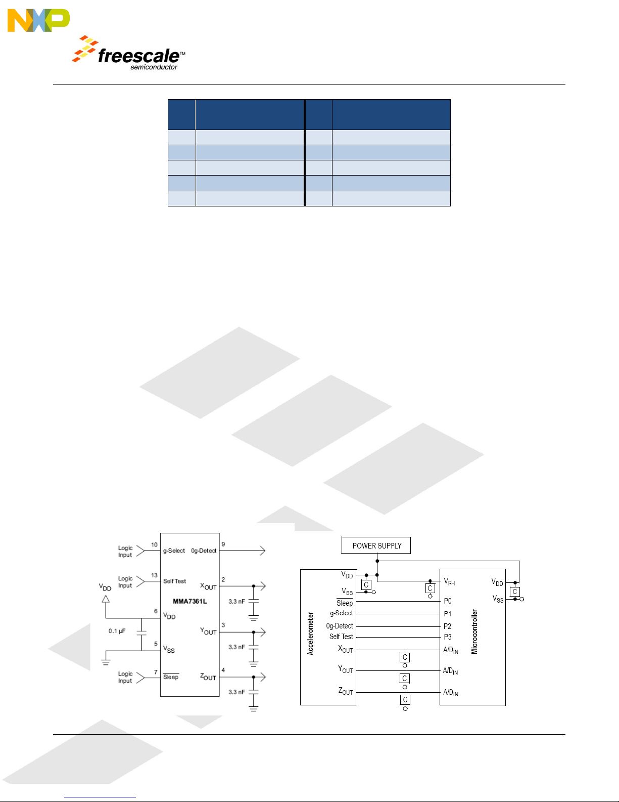
4.8 Accelerometer
An MMA7361L accelerometer is connected to three ADC inputs. There are 4 GPIO signals used to
configure the MMA7361L that are optional on the TWR-MCF5441X. The MMA7361L is wired as shown
here (as recommended in the MMA7361L Data Sheet):
MCF5441X Tower Module Hardware Specification Page 11 of 31
Page 12
Accelerometer
MCF54418
Configuration
Cut-Trace Pad
X
OUT
ADC_IN0
CT3
Y
OUT
ADC_IN1
CT6
Z
OUT
ADC_IN2
CT9
g-Select
PST[0]/GPIO2
CT7
nSleep
PST[1]/GPIO3
CT12
Self Test
PST[2]/GPIO4
CT4
0g-Detect
PST[3]/GPIO5
CT10
Figure 1 - MMA7361L Connection Diagram
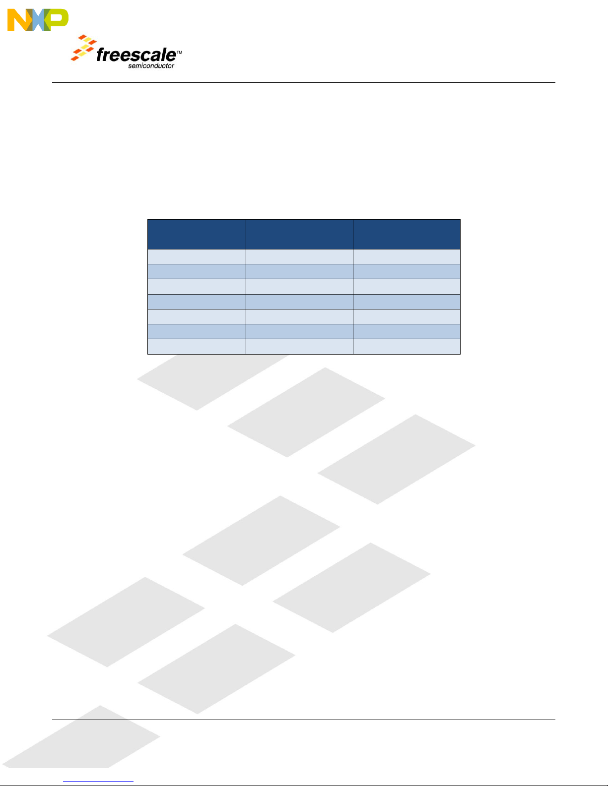
By default the control signals are not connected, but can be enabled using Cut-Trace pads. By default
the MMZ7361L is configured to operate in normal mode with 1.5g sensitivity and no self test
functionality.
The MMA7361L Accelerometer is connected as follows to the MCF54418 MPU:
Table 7 - Accelerometer Connection to MCF54418
By default the analog signals from the accelerometer are connected to the ADC channels 0-2 of the
MCF54418. If desired the connection to the accelerometer can be disconnected and the ADC channels
of the MCF54418 can be connected to the edge connectors for use on a module connected to the
TWR-ELEV.
To change the connection of ADC 0, 1, and 2 use the Cut-Trace pads CT3, CT6, and CT9 respectively.
Using a tool with a razor blade tip sever the connection between the pads 1 and 2 of each required
Cut-Trace implementation. Using a solder iron make a connection between pad 1 and pad 3.
By default the control signals for the MMA7361L accelerometer are not connected to the MCF54418.
To change the connection of the control signals (G-Select, nSleep, Self Test, and 0g-Detect) use the
respective Cut-Trace pads: CT7, CT12, CT4, and CT10. Using a solder iron create a connection between
pads 1 and 3.
Note that it is not possible to disconnect the default signals routing (PST[3:0]) for the these signals,
they are used for OSBDM functionality.
For more details regarding the Cut-Trace pad options and the pad numbering refer to the Cut-Trace
Pad section of this document.
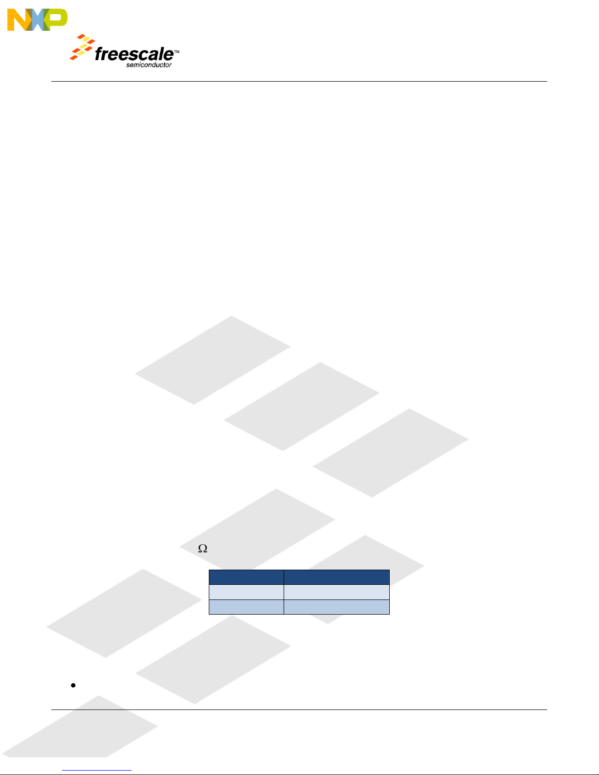
4.9 Potentiometer
The TWR-MCF5441X includes an on-board potentiometer to allow the user to simulate an analog
input.
MCF5441X Tower Module Hardware Specification Page 12 of 31
Page 13
Pin
Function
1
Output +
2
Output -
By default voltage level from the potentiometer is connected to the ADC channel 4 of the MCF54418.
If desired the connection to the potentiometer can be disconnected and the ADC channel of the
MCF54418 can be connected to the edge connectors for use on a module connected to the TWR-ELEV.
To change the connection of ADC 4 use the Cut-Trace pad CT14.
Using a tool with a razor blade tip sever the connection between the pads 1 and 2 of the CT14. Using
a solder iron make a connection between pad 1 and pad 3.
For more details regarding the Cut-Trace pad options and the pad numbering refer to the Cut-Trace
Pad section of this document.
4.10 Temperature Sensor
TWR-M54418 uses 1-wire interface (OWIO) to interact with temperature sensor Maxim DS18B20
digital thermometer. The sensor device is powered from TWR-MCF5441X’s 3.3V power circuit. The
Parasite-Powered method (where the power source is from data bus) is not used in this platform.
By default the One-Wire digital temperature sensor is connected to the OWIO port on the MCF54418.
Using Cut-Trace pad (CT15) the signal can be connected to the TWR-ELEV connector for connection to
additional One-Wire devices. This signal can also be used to control the operating mode of a CAN
transceiver on an external Tower System module. For the CAN use case, the will be configured as a
GPIO and should be disconnected from any One-Wire devices. To disconnect the signal from the onboard temperature sensor cut the trace between pads 1 and 2 of CT15.
For more details regarding the Cut-Trace pad options and the pad numbering refer to the Cut-Trace
Pad section of this document.
4.11 Audio Headers (DAC)
The TWR-MCF5441X uses National Semiconductor LM4889 Audio Power Amplifier to drive signal from
DAC1_OUT up to 1W into an 8 speaker.
4.12 User Interfaces
Three push buttons:
MCF5441X Tower Module Hardware Specification Page 13 of 31
Table 8 - J4 Headers
Page 14
MCF54418
Signal Name
LED
TWR-ELEV GPIO
Configuration
Cut-Trace Pad
GPIO_G0
LED1 (Amber)
GPIO9 (A9)
CT3
GPIO_G1
LED2 (Yellow)
GPIO7 (A11)
CT6
GPIO_G2
LED3 (Green)
GPIO1 (B21)
CT9
GPIO_G3
LED4 (Orange/Red)
GPIO5 (B52)
CT7
o IRQ1 (SW3)
o IRQ2 (SW5)
o MCU reset (SW2)
One 8-way DIP switch for controlling Parallel Reset Configuration
One 2-way DIP Switch for additional GPIOs (Assuming BDM DDATA[3:2] are disabled).
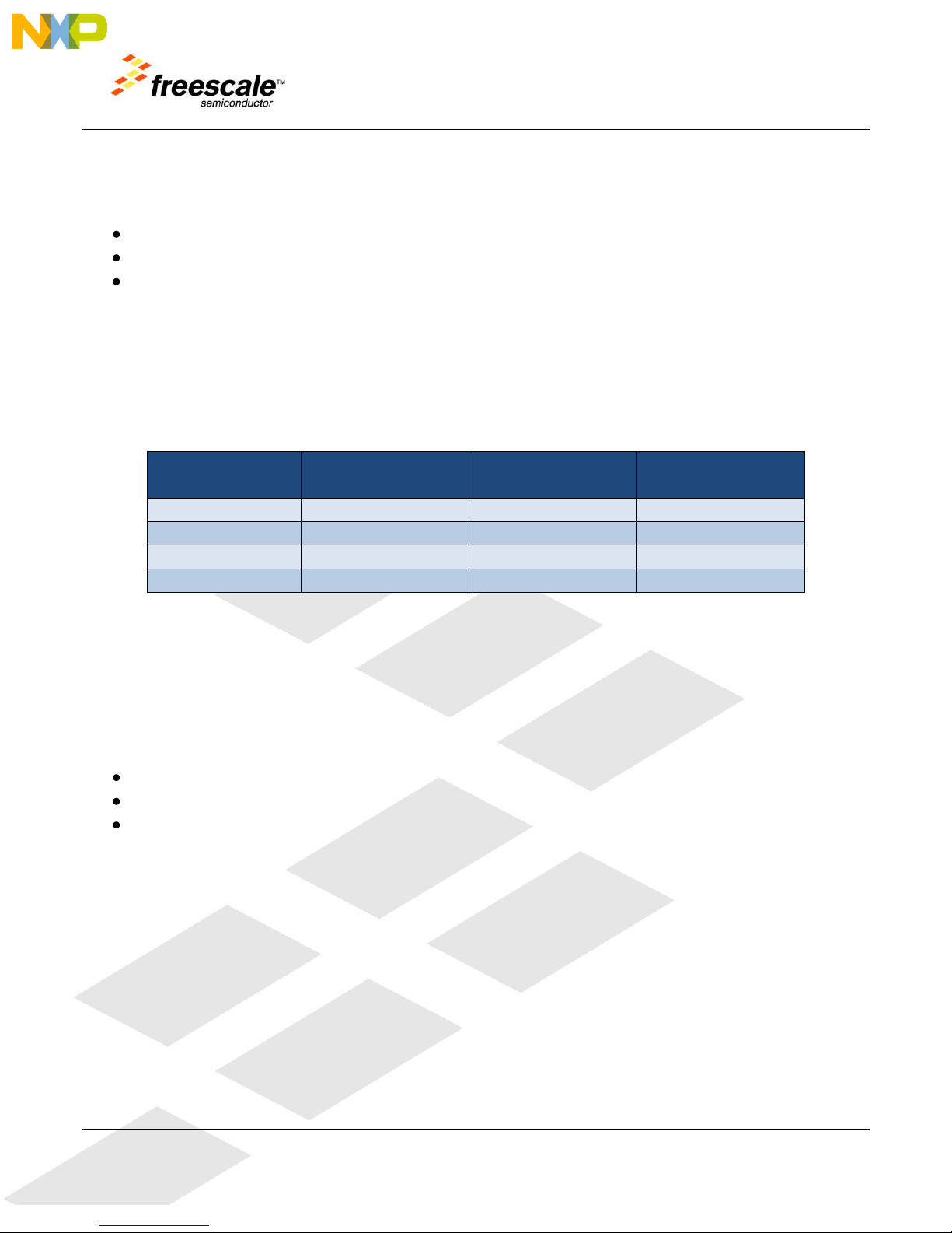
Four LEDs driven directly by MPU output pins.
The LEDs are concurrently connected to the LED’s and the edge connector for GPIO access to external
Tower System modules. If required the signals from the MCF54418 can be disconnected from either
the LED’s or the TWR-ELEV GPIO’s. The connection to the LEDs is made between pads 1 and 2. The
connection to the TWR-ELEV GPIO’s is made between pads 1 and 3. Refer to the table below for
details regarding which signal corresponds to which LED and TWR-ELEV GPIO.
For more details regarding the Cut-Trace pad options and the pad numbering refer to the Cut-Trace
Pad section of this document.
4.13 Reset Configuration
The TWR-MCF5441X has three boot mode options:
Boot with default configuration constants specified in the RCON register
Boot with NAND/NOR with configuration data specified by the Flexbus FB_AD[7:0] pins
Boot with configuration data obtained from an external SPI memory through the serial boot
facility.
The boot modes are determined by the jumper configuration of J5 at reset. Placing a jumper on pins
1-2 of J5 causes BOOTMOD[0] to be low (0). Placing a jumper on pins 3-4 of J5 causes BOOTMOD[1] to
be low (0). In the table below “ON” implies that the respective jumper is shunted.
MCF5441X Tower Module Hardware Specification Page 14 of 31
Page 15
BOOTMOD[1:0]
J5
3-4 : 1-2
Description
00
ON:ON
Boot from Flexbus with default (RCON)
01
ON:OFF
override default via data bus (FB_AD[7:0]) – NAND/FlexBus
The is the typical boot mode for the TWR-MCF5441X
10
OFF:ON
Override default and boot from serial boot facility with load
configuration and optional booting from internal SRAM. If
not booting from internal SRAM, serial RCON configuration
will decide the boot source at address 0 either from FlexBus
or NAND Flash.
11
OFF:OFF
Table 9 - J5 Headers
4.13.1 Default Configuration (J5: 3-4 and 1-2 = ON:ON)
If the BOOTMOD pins are 00 during reset, the MCF5441x’s RCON register determines the chip
configuration after reset, regardless of the states of the external data pins. The RCON register specifies
the following default configuration for the MCF5441x:
VCO clock is 50 MHz, CPU clock at 25 MHz
System bus clock is 12.5 MHz, FlexBus clock is 6.25 MHz
MCF5441X Tower Module Hardware Specification Page 15 of 31
Page 16
Override Pins in Reset
Function
SW1- DIP 1
Boot Memory
0 (Default)
NAND Flash
1
FlexBus
SW1-2
PLL mode
0
Disabled
1 (Default)
Enabled
SW1-3
Oscillator mode
0 (Default)
Crystal oscillator mode
1
Oscillator bypass mode
SW1-4
FB_ALE select
0
FB_TS_B
1 (Default)
FB_ALE
SW1-[6:5]
BOOT Port size
00
32-bit (32-bit muxed address)
01
8-bit (24-bit non-muxed address)
10 (Default)
16-bit (16-bit non-muxed address)
11
16-bit (16-bit non-muxed address)
SW1-[8:7]
PLL Multiplier
00 (Default)
Fvco = 10 x Fref
01
Fvco = 15 x Fref
10
Fvco = 16 x Fref
11
Fvco = 20 x Fref
4.13.2 Parallel Configuration (J5: 3-4 and 1-2 = ON:OFF)
If the BOOTMOD pins are 01 during reset, the MCF5441x configuration after reset is determined
according to the levels driven onto the FB_AD[7:0] pins. On the TWR-MCF5441X, the FB_AD[7:0] pins
are actively driven by two 4-bit buffers enabled when the MCF5441x RSTOUT signal is asserted. The
values driven by the buffer are set by the SW1 DIP switch settings. For SW1, a value of 0 implies that
the dip is switched “On”.
MCF5441X Tower Module Hardware Specification Page 16 of 31
Table 10 - SW1 8-way DIP switch
Page 17
BYTE Address
Data Contents
0x0
{0000, BLDIV[3:0]}
0x1
BLL[7:0]
0x2
BLL[15:8]
0x3
RCON[7:0]
0x4
RCON[15:8]
0x5
RCON[23:16]
0x6
RCON[31:24]
4.13.3 Serial Configuration (J5 OFF:OFF)
If the BOOTMOD pins are 11 during reset, then the chip configuration after reset is determined by
data obtained from an external SPI memory through serial boot using the SBF_DI, SBF_DO, SBF_CS,
and SBF_CLK signals. The internal configuration signals are driven to reflect the data being received
from the external SPI memory to allow for module configuration. See Table below.
Table 11 - Serial Boot Facility 7-BYTE Header
MCF5441X Tower Module Hardware Specification Page 17 of 31
Page 18
Override Serial RCON
Function
SBF_RCON[31:30]
BOOT Port size
00
32-bit (32-bit muxed address)
01
8-bit (24-bit non-muxed address)
10
16-bit (16-bit non-muxed address)
11
16-bit (16-bit non-muxed address)
SBF_RCON[29]
Boot Memory
0
NAND Flash
1
FlexBus
SBF_RCON[28:27]
Reserved
SBF_RCON[26]
FB_ALE select
0
FB_TS
1
FB_ALE
SBF_RCON[25]
Oscillator mode
0
Crystal oscillator mode
1
Oscillator bypass mode
SBF_RCON[24]
PLL mode
0
Disabled
1
Enabled
SBF_RCON[23:22]
PLL Reference Divider (PLL_CR[REFDIV])
00
1
01
2
Override Serial RCON
Function
10
Reserved
11
Reserved
SBF_RCON[21:16]
PLL reference Clock Multiplier (PLL_CR[FBKDIV])
SBF_RCON[15]
FlexBus Half Clock Enable
0
FlexBus Runs at Fsys/2
1
FlexBus Runs at Fsys/4
SBF_RCON[14:10]
NFC Clock Frequency (PLL_DR[OUTDIV5])
SBF_RCON[9:5]
Internal Bus Clock Frequency (PLL_DR[OUTDIV5])
SBF_RCON[4:0]
Core Bus Clock Frequency (PLL_DR[OUTDIV5])
Table 12 - Serial Boot Facility RCON Bit Definitions
MCF5441X Tower Module Hardware Specification Page 18 of 31
Page 19
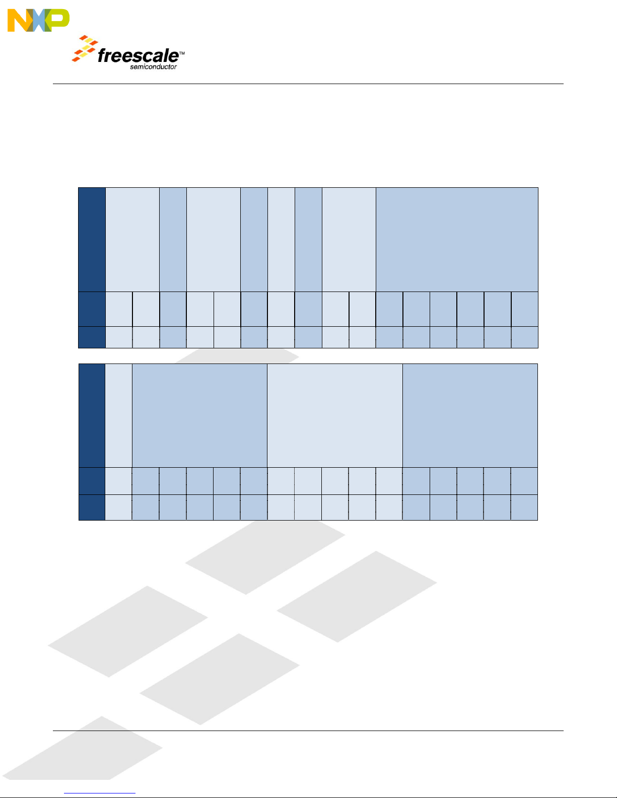
Serial RCON
BOOT Port size
Boot Memory
Reserved
FB_ALE select
Oscillator mode
PLL mode
PLL Reference
Divider
PLL Clock
Multiplier
Bit
31
30
29
28
27
26
25
24
23
22
21
20
19
18
17
16
Serial RCON
FlexBus Half Clock
NAND Flash
Controller Clock
Divider
Internal Bus Clock
Divider
Core Bus Clock
Divider
Bit
15
14
13
12
11
10 9 8 7 6 5 4 3 2 1 0
The value of BLL[15:0] of serial boot header (7-byte) will determine whether the code will continue to
load from SPI memory at offset 7 to internal SRAM and boot from internal SRAM. If the value of
BLL[15:0] is cleared, the serial boot facility will not continue to access SPI memory after offset 6.
Instead, it will depend on the SBF_RCON bit 29 to determine whether the code will continue to load at
address 0 either from FlexBus or NAND flash.
Table 13 - Easy Configurable Serial RCON
MCF5441X Tower Module Hardware Specification Page 19 of 31
Page 20
Jumpers /
Header
Description
J1
UART0 Header
J2
Clock Source (25Mhz/ External) Jumper
J3
UART4 Header
J4
Audio Speaker Header
J5
Boot Mode Jumpers
J6
BDM/JTAG mode Jumper
J7
JM60 BKGD/MS Header
J8
TCK/PSTCLK_OSBDM Jumper
J9
USB Mini B (OSBDM / PWR)
J10
JM60 IRQ (Boot Mode) Jumper
J11
26-pin BDM Header
J12
MCU Reset Jumper
J13
Primary Elevator Connection
J14
Secondary Elevator Connection
Switches /
Pushbuttons
Description
SW1
RCON Boot Settings Switch for BOOTMOD 01
SW2
MCU Reset Push Button
SW3
IRQ1 Push Button
SW4
User Input Switch (GPIOH0 / GPIOH1)
SW5
IRQ2 Puch Button
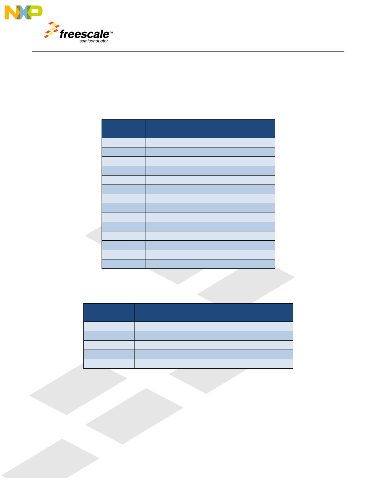
4.14 Jumpers, Switches
The TWR-MCF5441X implements a number of configuration jumpers, switches and headers. Refer to
this section for a quick overview of each. For more details refer to the specific section related to the
functionality of the specific jumper, switch, or header.
Table 14 - Jumpers / Headers Summary
Table 15- Switches / Push Buttons Summary
MCF5441X Tower Module Hardware Specification Page 20 of 31
Page 21
Trace/Cut Pad
Default Source Default Sink
Alternate Sink
Alternate Source /
Alternate Sink
1
43
2
Trace/Cut Pad
Default Source Default Sink
Alternate Sink
Alternate Source /
Alternate Sink
1
43
2
Trace/Cut Pad
Default Source Default Sink
Alternate Sink
Alternate Source /
Alternate Sink
1
43
2
Physical Implementation Schematic View
Default Connection
Alternate Connection
Dual Mode Connection
1
2
3
4
1
2
3
4
1
2
3
4
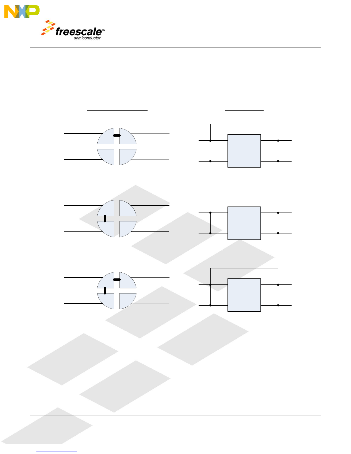
4.15 Cut/Trace Pads
Cut/Trace pads have been implemented on the TWR-MCF5441X in place of configuration jumpers to
ease board area constraints.
MCF5441X Tower Module Hardware Specification Page 21 of 31
Figure 2 - Cut/Trace Pad Details
Page 22
Cut-
Trace
Pads
Function
Primary Setting
Alternative Setting
CT1
UART5 TXD
1-2: Connects TXD to TWR-ELEV
1-3: Connects TXD to JM60
CT2
UART5 RXD
1-2: Connects RXD to TWR-ELEV
1-3: Connects RXD to JM60
CT3
ADC_0
1-2: Connects Accelerometer
X-axis to ADC_0
1-3: Connects ADC_0 to TWR-ELEV AN0
CT4
PST2
PST2 is connected to PST2 (redundant
connection)
1-3: Connects PST2 to Accelerometer Self_Test
CT5
GPIO PG3
1-2: Connects GPIO to TWR-ELEV
1-3: Connect GPIO to LED 4
CT6
ADC_1
1-2: Connects Accelerometer
Y-axis to ADC_1
1-3: Connects ADC_1 to TWR-ELEV AN1
CT7
PST0
PST0 is connected to PST0 (redundant
connection)
1-3: Connects PST0 to Accelerometer G-Select
CT8
GPIO PG2
1-2: Connects GPIO to TWR-ELEV
1-3: Connect GPIO to LED 3
CT9
ADC_2
1-2: Connects Accelerometer
Z-axis to ADC_2
1-3: Connects ADC_2 to TWR-ELEV AN2
CT10
PST3
PST3 is connected to PST3 (redundant
connection)
1-3: Connects PST3 to Accelerometer 0gDetect
CT11
GPIO PG1
1-2: Connects GPIO to TWR-ELEV
1-3: Connect GPIO to LED 2
CT12
PST1
PST1 is connected to PST1 (redundant
connection)
1-3: Connects PST1 to Accelerometer nSleep
CT13
GPIO PG0
1-2: Connects GPIO to TWR-ELEV
1-3: Connect GPIO to LED 1
CT14
ADC_4
1-2: Connects Potentiometer to ADC_4
1-3: Connects ADC_4 to TWR-ELEV AN4
CT15
OWIO /
GPIO PD3
3-4: Connects OWIO to on-board
temperature sensor
1-3-4: Connects OWIO to temperature sensor
and allows additional One-Wire to be
connected via TWR_ELEV
1-2-4: Connect s GPIO PD3 to CAN Silent
Mode pin on TWR-ELEV
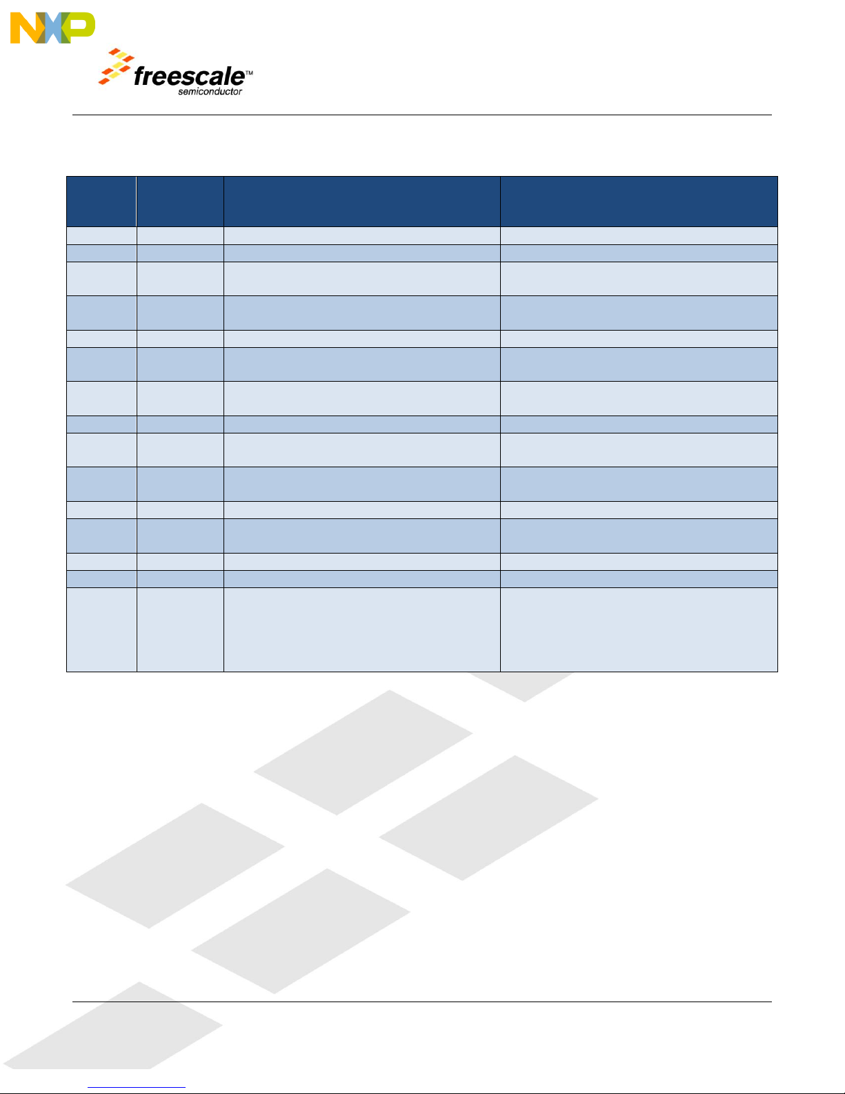
The TWR-MCF5441X implements the following Cut-Trace pads:
MCF5441X Tower Module Hardware Specification Page 22 of 31
Page 23

TWR-MCF5441X Primary Connector
Side A
Pin
Name
Group
Usage
Used
Jmp
A1
5V
Power
5.0V Power
X A2
GND
Power
Ground
X A3
3.3V
Power
3.3V Power
X A4
ELE_PS_SENSE
Power
Elevator Power Sense
X A5
GND
Power
Ground
X A6
GND
Power
Ground
X A7
SCL0
I2C 0
PB2/I2C0_SLC
X A8
SDA0
I2C 0
PB1/I2C0_SDA
X A9
GPIO9 / CTS1
GPIO/ UART
PG0/RGPIO
X A10
GPIO8 / SDHC_D2
GPIO/ SDHC1
PF1/SDHC_dat[2]
X A11
GPIO7 / SD_WP_DET
GPIO/ SD / SDHC1
PG4/RGPIO/SDHC_write_protect
X
Mechanical Key
A12
ETH_CRS
Ethernet
A13
ETH_MDC
Ethernet
PI1/RMII0_MDC
X A14
ETH_MDIO
Ethernet
PI0/RMII0_MDIO
X A15
ETH_RXCLK
Ethernet
A16
ETH_RXDV
Ethernet
PJ7/RMII0_CRS_DV
X A17
ETH_RXD3
Ethernet
A18
ETH_RXD2
Ethernet
A19
ETH_RXD1
Ethernet
PJ6/RMII0_RXD1
X A20
ETH_RXD0
Ethernet
PJ5/RMII0_RXD0
X A21
SSI_MCLK
SSI
PH4/SSI0_MCLK
X A22
SSI_BCLK
SSI
PH3/SSI0_BCLK
X A23
SSI_FS
SSI
PH5/SSI0_FS
X A24
SSI_RXD
SSI
PH7/SSI0_RXD
X A25
SSI_TXD
SSI
PH6/SSI0_TXD
X A26
GND
Power
Ground
X A27
AN3
ADC
ADC_IN3/DAC0_OUT
X
X
A28
AN2
ADC
ADC_IN2
X X A29
AN1
ADC
ADC_IN1
X X A30
AN0
ADC
ADC_IN0
X X A31
GND
Power
Ground
X A32
DAC0
DAC
A33
TMR1
Timer
PD1/RGPIO/T2IN/T2OUT
X A34
TMR0
Timer
PD0/RGPIO/T1IN/T1OUT
X A35
GPIO6
GPIO
PB5/GPIO
X A36
3.3V
Power
3.3V Power
X A37
PWM3
PWM
PF1/PWM_B1
X A38
PWM2
PWM
PF2/PWM_A1
X
A39
PWM1
PWM
PG6/PWM_B0
X
A40
PWM0
PWM
PG5/PWM_A0
X
Tower Elevator Connections
MCF5441X Tower Module Hardware Specification Page 23 of 31
Page 24

TWR-MCF5441X Primary Connector
Side A
Pin
Name
Group
Usage
Used
Jmp
A41
RXD0
UART 0
PE5/RGPIO/UART6_RXD
X X A42
TXD0
UART 0
PE6/RGPIO/UART6_TXD
X X A43
RXD1
UART 1
PE1/RGPIO/UART5_RXD
X X A44
TXD1
UART 1
PE2/RGPIO/UART5_TXD
X X A45
GPIO
GPIO
A46
GPIO
GPIO
A47
GPIO
GPIO
A48
GPIO
GPIO
A49
GND
Power
Ground
X A50
GPIO
GPIO
A51
GPIO
GPIO
A52
GPIO
GPIO
A53
GPIO
GPIO
A54
USB0_DM
USB 0
USBO_DM
X A55
USB0_DP
USB 0
USBO_DP
X A56
USB0_ID
USB 0
A57
USB0_VBUS
USB 0
A58
TMR7
Timer
A59
TMR6
Timer
A60
TMR5
Timer
A61
TMR4
Timer
A62
RSTIN_b
Reset
RESET
X A63
RSTOUT_b
Reset
RSTOUT
X A64
CLKOUT0
Clock
PB7/FB_CLK
X A65
GND
Power
Ground
X A66
FB_AD14
Flexbus
FB_AD14
X A67
FB_AD13
Flexbus
FB_AD13
X A68
FB_AD12
Flexbus
FB_AD12
X A69
FB_AD11
Flexbus
FB_AD11
X A70
FB_AD10
Flexbus
FB_AD10
X A71
FB_AD9
Flexbus
FB_AD9
X A72
FB_AD8
Flexbus
FB_AD8
X A73
FB_AD7
Flexbus
FB_AD7
X A74
FB_AD6
Flexbus
FB_AD6
X A75
FB_AD5
Flexbus
FB_AD5
X A76
FB_AD4
Flexbus
FB_AD4
X A77
FB_AD3
Flexbus
FB_AD3
X A78
FB_AD2
Flexbus
FB_AD2
X A79
FB_AD1
Flexbus
FB_AD1
X A80
FB_AD0
Flexbus
FB_AD0
X A81
GND
Power
Ground
X
A82
3.3V
Power
3.3V Power
X
MCF5441X Tower Module Hardware Specification Page 24 of 31
Page 25

TWR-MCF5441X Primary Connector
Side B
Pin
Name
Group
Usage
Used
Jmp
B1
5V
Power
5.0V Power
X B2
GND
Power
Ground
X B3
3.3V
Power
3.3V Power
X B4
ELE_PS_SENSE
Power
Elevator Power Sense
X B5
GND
Power
Ground
X B6
GND
Power
Ground
X B7
SPI1_CLK / SDHC1_CLK
SPI 1 / SDHC1
PG5/SDHC_clk
X B8
SPI1_CS1 / SDHC1_CS1
SPI 1 / SDHC1
B9
SPI1_CS0 / SDHC1_CS0
SPI 1 / SDHC1
PF2/SDHC_dat[3]
X B10
SPI1_MOSI / SDHC1_CMD
SPI 1 / SDHC1
PG6/SDHC_cmd
X B11
SPI1_MISO / SDHC1_D0
SPI 1 / SDHC1
PG7/SDHC_dat[0]
X
Mechanical Key
B12
ETH_COL
Ethernet
B13
ETH_RXER
Ethernet
PJ4/RMII0_RXER
X B14
ETH_TXCLK
Ethernet
B15
ETH_TXEN
Ethernet
PJ0/RMII0_TXEN
X B16
ETH_TXER
Ethernet
B17
ETH_TXD3
Ethernet
B18
ETH_TXD2
Ethernet
B19
ETH_TXD1
Ethernet
PJ3/RMII0_TXD1
X B20
ETH_TXD0
Ethernet
PJ2/RMII0_TXD0
X B21
GPIO1 / RTS1
GPIO/ UART
PG2/RGPIO
X B22
GPIO2 / SDHC1_D1
GPIO/ SDHC1
PF0/SDHC_dat[1]
X B23
GPIO3
GPIO
B24
CLKIN0
Clock
RMII_REF_CLK
X X B25
CLKOUT1
Clock
B26
GND
Power
Ground
X B27
AN7
ADC
B28
AN6
ADC
ADC_IN6
X B29
AN5
ADC
ADC_IN5
X B30
AN4
ADC
ADC_IN4
X X B31
GND
Power
Ground
X B32
DAC1
DAC
B33
TMR3
Timer
B34
TMR2
Timer
B35
GPIO4
GPIO
PB6/GPIO
X B36
3.3V
Power
3.3V Power
X B37
PWM7
PWM
B38
PWM6
PWM
B39
PWM5
PWM
PG7/PWM_B2
X
B40
PWM4
PWM
PF0/PWM_A2
X
B41
CANRX
CAN
PC7/CAN1_RX
X
MCF5441X Tower Module Hardware Specification Page 25 of 31
Page 26

TWR-MCF5441X Primary Connector
Side B
Pin
Name
Group
Usage
Used
Jmp
B42
CANTX
CAN
PB0/CAN1_TX
X B43
1WIRE
1-Wire
B44
SPI0_MISO
SPI 0
PD5/DSPI0_SIN/SBF_DI
X B45
SPI0_MOSI
SPI 0
PD4/DSPI0_SOUT/SBF_DO
X B46
SPI0_CS0
SPI 0
PD7/DSPI0_PCS0/SS
X B47
SPI0_CS1
SPI 0
PC0/DSPI0_PCS1/BSF_CS
X B48
SPI0_CLK
SPI 0
PD6/DSPI0_SCK/SBF_CK
X B49
GND
Power
Ground
X B50
SCL1
I2C 1
PE0/I2C5_SCL
X B51
SDA1
I2C 1
PF7/I2C5_SDA
X B52
GPIO5
GPIO
PG3/RGPIO
X B53
USB_DP_PDOWN
USB
PI6
X B54
USB_DM_PDOWN
USB
PI7
X B55
IRQ_H
Interrupt
PC6/IRQ7
X B56
IRQ_G
Interrupt
PC6/IRQ7
X B57
IRQ_F
Interrupt
PC4/IRQ4
X B58
IRQ_E
Interrupt
PC4/IRQ4
X B59
IRQ_D
Interrupt
PC3/IRQ3
X B60
IRQ_C
Interrupt
PC3/IRQ3
X B61
IRQ_B
Interrupt
PC2/IRQ2
X B62
IRQ_A
Interrupt
PC1/IRQ1
X B63
FB_ALE/FB_CS1_b
Flexbus
PA7/FB_ALE
X B64
FB_CS0_b
Flexbus
PB3/FB_CS0
X B65
GND
Power
Ground
X B66
FB_AD15
Flexbus
FB_AD15
X B67
FB_AD16
Flexbus
FB_AD16/NFC_IO0
X B68
FB_AD17
Flexbus
FB_AD17/NFC_IO1
X B69
FB_AD18
Flexbus
FB_AD18/NCF_IO2
X B70
FB_AD19
Flexbus
FB_AD19/NFC_IO3
X B71
FB_R/W_b
Flexbus
PA5/FB_RW/NFC_WE
X B72
FB_OE_b
Flexbus
PA6/FB_OE/NFC_RE
X B73
FB_D7
Flexbus
FB_AD31
X B74
FB_D6
Flexbus
FB_AD30
X B75
FB_D5
Flexbus
FB_AD29
X B76
FB_D4
Flexbus
FB_AD28
X B77
FB_D3
Flexbus
FB_AD27
X B78
FB_D2
Flexbus
FB_AD26
X B79
FB_D1
Flexbus
FB_AD25
X B80
FB_D0
Flexbus
FB_AD24
X B81
GND
Power
Ground
X B82
3.3V
Power
3.3V Power
X
MCF5441X Tower Module Hardware Specification Page 26 of 31
Page 27

TWR-MCF5441X Secondary Connector
Side C
Pin
Name
Group
Usage
Used
Jmp
C1
5V
Power
5.0V Power
X C2
GND
Power
Ground
X C3
3.3V
Power
3.3V Power
X C4
3.3V
Power
3.3V Power
X C5
GND
Power
Ground
X C6
GND
Power
Ground
X C7
SCL2
I2C 2
C8
SDA2
I2C 2
C9
GPIO25
GPIO
C10
USB_STOP
ULPI
ULPI_STP
X C11
USB_CLK
ULPI
USB_CLKIN
X
Mechanical Key
C12
GPIO
GPIO
C13
ETH_MDC
Ethernet
RMII1_MDC
X C14
ETH_MDIO
Ethernet
RMII1_MDIO
X C15
ETH_RXCLK
Ethernet
C16
ETH_RXDV
Ethernet
RMII1_CRS_DV
X C17
GPIO
GPIO
C18
GPIO
GPIO
C19
ETH_RXD1
Ethernet
RMII1_RXD1
X C20
ETH_RXD0
Ethernet
RMII1_RXD0
X C21
USB_DATA0
ULPI
ULPI_DATA0
X C22
USB_DATA1
ULPI
ULPI_DATA1
X C23
USB_DATA2
ULPI
ULPI_DATA2
X C24
USB_DATA3
ULPI
ULPI_DATA3
X C25
USB_DATA4
ULPI
ULPI_DATA4
X C26
GND
Power
Ground
X C27
AN11
ADC
C28
AN10
ADC
C29
AN9
ADC
C30
AN8
ADC
C31
GND
Power
Ground
X C32
GPIO
GPIO
C33
TMR9
Timer
C34
TMR8
Timer
C35
GPIO
GPIO
C36
3.3V
Power
3.3V Power
X C37
PWM11
PWM
C38
PWM10
PWM
C39
PWM9
PWM
C40
PWM8
PWM
C41
RXD2
UART 2
PE4/UART2_RXD
X
X
MCF5441X Tower Module Hardware Specification Page 27 of 31
Page 28

TWR-MCF5441X Secondary Connector
Side C
Pin
Name
Group
Usage
Used
Jmp
C42
TXD2
UART 2
PE3/UART2_TXD
X X C43
RTS2
UART 2
PE5/RGPIO/UART2_RTS
X X C44
CTS2
UART 2
PE6/RGPIO/UART2_CTS
X X C45
RXD3
UART 3
C46
TXD3
UART 3
C47
RTS3
UART 3
C48
CTS3
UART 3
C49
GND
Power
Ground
X C50
LCD_D4 / LCD4
Display
C51
LCD_D5 / LCD5
Display
C52
LCD_D6 / LCD6
Display
C53
LCD_D7 / LCD7
Display
C54
LCD_D8 / LCD8
Display
C55
LCD_D9 / LCD9
Display
C56
LCD_D10 / LCD10
Display
C57
LCD_D11 / LCD11
Display
C58
TMR16
Timer
C59
TMR15
Timer
C60
TMR14
Timer
C61
TMR13
Timer
C62
LCD_D15 / LCD15
Display
C63
LCD_D16 / LCD16
Display
C64
LCD_D17 / LCD17
Display
C65
GND
Power
Ground
X C66
FB_BE3 / LCD28
Flexbus / Display
C67
FB_BE2 / LCD29
Flexbus / Display
C68
FB_BE1 / LCD30
Flexbus / Display
C69
FB_BE0 / LCD31
Flexbus / Display
C70
FB_TSIZE0 / LCD32
Flexbus / Display
PA0/FB_TSIZ[0]
X C71
FB_TSIZE1 / LCD33
Flexbus / Display
PA1/FB_TSIZ[1]
X C72
FB_TS / LCD34
Flexbus / Display
C73
FB_TBST / LCD35
Flexbus / Display
C74
TB_TA / LCD36
Flexbus / Display
C75
FB_CS4 / LCD37
Flexbus / Display
C76
FB_CS3 / LCD38
Flexbus / Display
C77
FB_CS2 / LCD39
Flexbus / Display
C78
FB_CS1 / LCD40
Flexbus / Display
C79
GPIO / LCD41
GPIO
C80
LCD_D23 / LCD23
Display
C81
GND
Power
Ground
X C82
3.3V
Power
3.3V Power
MCF5441X Tower Module Hardware Specification Page 28 of 31
Page 29

TWR-MCF5441X Secondary Connector
Side D
Pin
Name
Group
Usage
Used
Jmp
D1
5V
Power
5.0V Power
X D2
GND
Power
Ground
X D3
3.3V
Power
3.3V Power
X D4
3.3V
Power
Elevator Power Sense
X D5
GND
Power
Ground
X D6
GND
Power
Ground
X D7
SPI2_CLK
SPI 2
D8
SPI2_CS1
SPI 2
D9
SPI2_CS0
SPI 2
D10
SPI2_MOSI
SPI 2
D11
SPI2_MISO
SPI 2
Mechanical Key
D12
ETH_COL
Ethernet
D13
ETH_RXER
Ethernet
RMII1_RXER
X D14
ETH_TXCLK
Ethernet
D15
ETH_TXEN
Ethernet
RMII1_TXEN
X D16
GPIO
GPIO
D17
GPIO
GPIO
PH0/DIP Switches
X D18
GPIO
GPIO
PH1/DIP Switches
X D19
ETH_TXD1
Ethernet
RMII1_TXD1
X D20
ETH_TXD0
Ethernet
RMII1_TXD0
X D21
ULPI_NEXT
ULPI
PE7/RGPIO/ULPI_NXT
X D22
USB_DIR
ULPI
PD2/RGPIO/ULPI_DIR
X D23
USB_DATA5
ULPI
ULPI_DATA5
X D24
USB_DATA6
ULPI
ULPI_DATA6
X D25
USB_DATA7
ULPI
ULPI_DATA7
X D26
GND
Power
Ground
X D27
LCD_HSYNC / LCD24
Display
D28
LCD_VSYNC / LCD25
Display
D29
AN13
ADC
D30
AN12
ADC
D31
GND
Power
Ground
X D32
LCD_CLK / LCD26
Display
D33
TMR11
Timer
D34
TMR10
Timer
D35
GPIO
GPIO
D36
3.3V
Power
3.3V Power
X D37
PWM15
PWM
D38
PWM14
PWM
D39
PWM13
PWM
D40
PWM12
PWM
D41
CANRX1
CAN
MCF5441X Tower Module Hardware Specification Page 29 of 31
Page 30

TWR-MCF5441X Secondary Connector
Side D
Pin
Name
Group
Usage
Used
Jmp
D42
CANTX1
CAN
D43
GPIO
GPIO
D44
LCD_OE / LCD27
Display
D45
LCD_D0 / LCD0
Display
D46
LCD_D1 / LCD1
Display
D47
LCD_D2 / LCD2
Display
D48
LCD_D3 / LCD3
Display
D49
GND
Power
Ground
X D50
GPIO
GPIO
D51
GPIO
GPIO
D52
LCD_D12 / LCD12
Display
D53
LCD_D13 / LCD13
Display
D54
LCD_D14 / LCD14
Display
D55
IRQ_P
Interrupt
D56
IRQ_O
Interrupt
D57
IRQ_N
Interrupt
D58
IRQ_M
Interrupt
D59
IRQ_L
Interrupt
D60
IRQ_K
Interrupt
D61
IRQ_J
Interrupt
D62
IRQ_I
Interrupt
D63
LCD_D18 / LCD18
Display
D64
LCD_D19 / LCD19
Display
D65
GND
Power
Ground
X D66
FB_AD20 / LCD42
Flexbus / Display
FB_AD20
X D67
FB_AD21 / LCD43
Flexbus / Display
FB_AD21
X D68
FB_AD22 / LCD44
Flexbus / Display
FB_AD22
X D69
FB_AD23 / LCD45
Flexbus / Display
FB_AD23
X D70
FB_AD24 / LCD46
Flexbus / Display
FB_AD24
X D71
FB_AD25 / LCD47
Flexbus / Display
FB_AD25
X D72
FB_AD26 / LCD48
Flexbus / Display
FB_AD26
X D73
FB_AD27 / LCD49
Flexbus / Display
FB_AD27
X D74
FB_AD28 / LCD50
Flexbus / Display
FB_AD28
X D75
FB_AD29 / LCD51
Flexbus / Display
FB_AD29
X D76
FB_AD30 / LCD52
Flexbus / Display
FB_AD30
X D77
FB_AD31 / LCD53
Flexbus / Display
FB_AD31
X D78
LCD_D20 / LCD20
Display
D79
LCD_D21 / LCD21
Display
D80
LCD_D22 / LCD22
Display
D81
GND
Power
Ground
X D82
3.3V
Power
3.3V Power
X
MCF5441X Tower Module Hardware Specification Page 30 of 31
Page 31

Freescale™ and the Freescale l ogo are trademarks of
Freescale Semiconductor, Inc. All other product or service names
are the property of their respective owners.
© Freescale Semiconductor, Inc. 2008. All rights reserved.
MCF5441X Tower Module Hardware Specification Page 31 of 31
 Loading...