

Page 1

S12
Microcontrollers
freescale.com
MC9S12VR-Family
Reference Manual
MC9S12VRRMV2
Rev. 2.2
June 20, 2011
Downloaded from Elcodis.com electronic components distributor
Page 2

MC9S12VR Family Reference Manual, Rev. 2.2
Freescale Semiconductor 2
Preliminary - Subject to Change Without Notice
To provide the most up-to-date information, the revision of our documents on the World Wide Web will be
the most current. Your printed copy may be an earlier revision. To verify you have the latest information
available, refer to:
http://freescale.com/
A full list of family members and options is included in the appendices.
The following revision history table summarizes changes contained in this document.
This document contains information for all constituent modules, with the exception of the CPU. For CPU
information please refer to CPU12-1 in the CPU12 & CPU12X Reference Manual.
Table 0-1. Revision History
Date
Revision
Level
Description
13-December 2010 Rev 1.0 • Initial
11-April-2011 Rev 2.0
• See Revision History Table 1-1
• See Revision History Table 2-1
• See Revision History Table 16-1
• See Revision History Table 4-1
• SPI thresholds for delay measurement corrected (35%/65%) see Table K-1
• All SPI timing data classified D ( Derived from Simulations) see Table K-2 &
Table K-3
• VSUP range corrected see Table G-2 item number 3
• VSUP range corrected see Table H-1 item number 2
• Added registers for PWM channels 2-7 to O.1 Detailed Register Map
11-May-2011 Rev 2.1
• See revision History Table 14-1
• See revision History Table 13-1
• See revision History Table 2-1
• Pull up spec
RESET pin Table A-8 item 14
• HSDRV electricals Table D-2 item 2
• LSDRV electricals Table H-1 item 4
• Battery sensor electricals Table I-2I
• Voltage regulator electricals Table B-1,item 5 and 15
• Added M.1.18
• Minor corrections in Clock, Reset and Power Management (S12CPMU_UHV)
20-June-2011 Rev 2.2 • Removed “Freescale Confidential Proprietary”
Downloaded from Elcodis.com electronic components distributor
Page 3

MC9S12VR Family Reference Manual, Rev. 2.2
Freescale Semiconductor 3
Preliminary - Subject to Change Without Notice
Chapter 1 Device Overview MC9S12VR-Family . . . . . . . . . . . . . . . . . . . .21
Chapter 2 Port Integration Module (S12VRPIMV2) . . . . . . . . . . . . . . . . . .49
Chapter 3 S12G Memory Map Controller (S12GMMCV1) . . . . . . . . . . . .105
Chapter 4 Clock, Reset and Power Management (S12CPMU_UHV) . . .119
Chapter 5 Background Debug Module (S12SBDMV1) . . . . . . . . . . . . . .175
Chapter 6 S12S Debug Module (S12SDBGV2) . . . . . . . . . . . . . . . . . . . .199
Chapter 7 Interrupt Module (S12SINTV1). . . . . . . . . . . . . . . . . . . . . . . . .243
Chapter 8 Analog-to-Digital Converter (ADC12B6CV2) . . . . . . . . . . . . .251
Chapter 9 Pulse-Width Modulator (S12PWM8B8CV2) . . . . . . . . . . . . . .277
Chapter 10 Serial Communication Interface (S12SCIV5) . . . . . . . . . . . . .307
Chapter 11 Serial Peripheral Interface (S12SPIV5) . . . . . . . . . . . . . . . . . .345
Chapter 12 Timer Module (TIM16B8CV3). . . . . . . . . . . . . . . . . . . . . . . . . .371
Chapter 13 High-Side Drivers - HSDRV (S12HSDRV1) . . . . . . . . . . . . . . .399
Chapter 14 Low-Side Drivers - LSDRV (S12LSDRV1). . . . . . . . . . . . . . . . 411
Chapter 15 LIN Physical Layer (S12LINPHYV1) . . . . . . . . . . . . . . . . . . . .425
Chapter 16 Supply Voltage Sensor - (BATSV2). . . . . . . . . . . . . . . . . . . . .443
Chapter 17 64 KByte Flash Module (S12FTMRG64K512V1). . . . . . . . . . .457
Appendix A MCU Electrical Specifications. . . . . . . . . . . . . . . . . . . . . . . . . 509
Appendix B VREG Electrical Specifications. . . . . . . . . . . . . . . . . . . . . . . . 523
Appendix C ATD Electrical Specifications . . . . . . . . . . . . . . . . . . . . . . . . .525
Appendix D HSDRV Electrical Specifications. . . . . . . . . . . . . . . . . . . . . . .531
Appendix E PLL Electrical Specifications . . . . . . . . . . . . . . . . . . . . . . . . .533
Appendix F IRC Electrical Specifications. . . . . . . . . . . . . . . . . . . . . . . . . . 535
Appendix G LINPHY Electrical Specifications . . . . . . . . . . . . . . . . . . . . . . 537
Appendix H LSDRV Electrical Specifications. . . . . . . . . . . . . . . . . . . . . . . 541
Appendix I BATS Electrical Specifications . . . . . . . . . . . . . . . . . . . . . . . .543
Appendix J PIM Electrical Specifications. . . . . . . . . . . . . . . . . . . . . . . . . .547
Appendix K SPI Electrical Specifications . . . . . . . . . . . . . . . . . . . . . . . . . .549
Downloaded from Elcodis.com electronic components distributor
Page 4

MC9S12VR Family Reference Manual, Rev. 2.2
4 Freescale Semiconductor
Preliminary - Subject to Change Without Notice
Appendix L XOSCLCP Electrical Specifications . . . . . . . . . . . . . . . . . . . .555
Appendix M FTMRG Electrical Specifications . . . . . . . . . . . . . . . . . . . . . .557
Appendix N Package Information . . . . . . . . . . . . . . . . . . . . . . . . . . . . . . . . 565
Appendix O Detailed Register Address Map. . . . . . . . . . . . . . . . . . . . . . . .571
Downloaded from Elcodis.com electronic components distributor
Page 5

MC9S12VR Family Reference Manual, Rev. 2.2
Freescale Semiconductor 5
Preliminary - Subject to Change Without Notice
Chapter 1
Device Overview MC9S12VR-Family
1.1 Introduction . . . . . . . . . . . . . . . . . . . . . . . . . . . . . . . . . . . . . . . . . . . . . . . . . . . . . . . . . . . . . . . . . . 21
1.2 Features . . . . . . . . . . . . . . . . . . . . . . . . . . . . . . . . . . . . . . . . . . . . . . . . . . . . . . . . . . . . . . . . . . . . . 22
1.2.1 MC9S12VR-Family Member Comparison . . . . . . . . . . . . . . . . . . . . . . . . . . . . . . . . . . . 22
1.3 Chip-Level Features . . . . . . . . . . . . . . . . . . . . . . . . . . . . . . . . . . . . . . . . . . . . . . . . . . . . . . . . . . . . 23
1.4 Module Features . . . . . . . . . . . . . . . . . . . . . . . . . . . . . . . . . . . . . . . . . . . . . . . . . . . . . . . . . . . . . . . 24
1.4.1 HCS12 16-Bit Central Processor Unit (CPU) . . . . . . . . . . . . . . . . . . . . . . . . . . . . . . . . . 24
1.4.2 On-Chip Flash with ECC . . . . . . . . . . . . . . . . . . . . . . . . . . . . . . . . . . . . . . . . . . . . . . . . . 24
1.4.3 On-Chip SRAM . . . . . . . . . . . . . . . . . . . . . . . . . . . . . . . . . . . . . . . . . . . . . . . . . . . . . . . .24
1.4.4 Main External Oscillator (XOSCLCP) . . . . . . . . . . . . . . . . . . . . . . . . . . . . . . . . . . . . . . 25
1.4.5 Internal RC Oscillator (IRC) . . . . . . . . . . . . . . . . . . . . . . . . . . . . . . . . . . . . . . . . . . . . . . 25
1.4.6 Internal Phase-Locked Loop (IPLL) . . . . . . . . . . . . . . . . . . . . . . . . . . . . . . . . . . . . . . . . 25
1.4.7 Clock and Power Management Unit (CPMU) . . . . . . . . . . . . . . . . . . . . . . . . . . . . . . . . . 25
1.4.8 System Integrity Support . . . . . . . . . . . . . . . . . . . . . . . . . . . . . . . . . . . . . . . . . . . . . . . . . 25
1.4.9 Timer (TIM) . . . . . . . . . . . . . . . . . . . . . . . . . . . . . . . . . . . . . . . . . . . . . . . . . . . . . . . . . . . 26
1.4.10 Pulse Width Modulation Module (PWM) . . . . . . . . . . . . . . . . . . . . . . . . . . . . . . . . . . . . 26
1.4.11 LIN physical layer transceiver (LINPHY) . . . . . . . . . . . . . . . . . . . . . . . . . . . . . . . . . . . . 26
1.4.12 Serial Peripheral Interface Module (SPI) . . . . . . . . . . . . . . . . . . . . . . . . . . . . . . . . . . . . . 26
1.4.13 Serial Communication Interface Module (SCI) . . . . . . . . . . . . . . . . . . . . . . . . . . . . . . . . 26
1.4.14 Analog-to-Digital Converter Module (ATD) . . . . . . . . . . . . . . . . . . . . . . . . . . . . . . . . . . 27
1.4.15 Supply Voltage Sense (BATS) . . . . . . . . . . . . . . . . . . . . . . . . . . . . . . . . . . . . . . . . . . . . . 27
1.4.16 On-Chip Voltage Regulator system (VREG) . . . . . . . . . . . . . . . . . . . . . . . . . . . . . . . . . . 27
1.4.17 Low-side drivers (LSDRV) . . . . . . . . . . . . . . . . . . . . . . . . . . . . . . . . . . . . . . . . . . . . . . . 28
1.4.18 High-side drivers (HSDRV) . . . . . . . . . . . . . . . . . . . . . . . . . . . . . . . . . . . . . . . . . . . . . . . 28
1.4.19 Background Debug (BDM) . . . . . . . . . . . . . . . . . . . . . . . . . . . . . . . . . . . . . . . . . . . . . . . 28
1.4.20 Debugger (DBG) . . . . . . . . . . . . . . . . . . . . . . . . . . . . . . . . . . . . . . . . . . . . . . . . . . . . . . . 28
1.5 Block Diagram . . . . . . . . . . . . . . . . . . . . . . . . . . . . . . . . . . . . . . . . . . . . . . . . . . . . . . . . . . . . . . . . 29
1.6 Family Memory Map . . . . . . . . . . . . . . . . . . . . . . . . . . . . . . . . . . . . . . . . . . . . . . . . . . . . . . . . . . . 30
1.6.1 Part ID Assignments . . . . . . . . . . . . . . . . . . . . . . . . . . . . . . . . . . . . . . . . . . . . . . . . . . . .33
1.7 Signal Description and Device Pinouts . . . . . . . . . . . . . . . . . . . . . . . . . . . . . . . . . . . . . . . . . . . . . 33
1.7.1 Pin Assignment Overview . . . . . . . . . . . . . . . . . . . . . . . . . . . . . . . . . . . . . . . . . . . . . . . . 33
1.7.2 Detailed Signal Descriptions . . . . . . . . . . . . . . . . . . . . . . . . . . . . . . . . . . . . . . . . . . . . . . 34
1.7.3 Power Supply Pins . . . . . . . . . . . . . . . . . . . . . . . . . . . . . . . . . . . . . . . . . . . . . . . . . . . . . .37
1.8 Device Pinouts . . . . . . . . . . . . . . . . . . . . . . . . . . . . . . . . . . . . . . . . . . . . . . . . . . . . . . . . . . . . . . . . 38
1.8.1 Pinout 48-pin LQFP . . . . . . . . . . . . . . . . . . . . . . . . . . . . . . . . . . . . . . . . . . . . . . . . . . . . .39
1.8.2 Pinout 32-pin LQFP . . . . . . . . . . . . . . . . . . . . . . . . . . . . . . . . . . . . . . . . . . . . . . . . . . . . .40
1.9 Modes of Operation . . . . . . . . . . . . . . . . . . . . . . . . . . . . . . . . . . . . . . . . . . . . . . . . . . . . . . . . . . . . 43
1.9.1 Chip Configuration Summary . . . . . . . . . . . . . . . . . . . . . . . . . . . . . . . . . . . . . . . . . . . . . 43
1.9.2 Low Power Operation . . . . . . . . . . . . . . . . . . . . . . . . . . . . . . . . . . . . . . . . . . . . . . . . . . . 43
1.10 Security . . . . . . . . . . . . . . . . . . . . . . . . . . . . . . . . . . . . . . . . . . . . . . . . . . . . . . . . . . . . . . . . . . . . . . 44
1.11 Resets and Interrupts . . . . . . . . . . . . . . . . . . . . . . . . . . . . . . . . . . . . . . . . . . . . . . . . . . . . . . . . . . . 44
1.11.1 Resets . . . . . . . . . . . . . . . . . . . . . . . . . . . . . . . . . . . . . . . . . . . . . . . . . . . . . . . . . . . . . . . . 44
1.11.2 Interrupt Vectors . . . . . . . . . . . . . . . . . . . . . . . . . . . . . . . . . . . . . . . . . . . . . . . . . . . . . . . . 45
1.11.3 Effects of Reset . . . . . . . . . . . . . . . . . . . . . . . . . . . . . . . . . . . . . . . . . . . . . . . . . . . . . . . . 46
Downloaded from Elcodis.com electronic components distributor
Page 6

MC9S12VR Family Reference Manual, Rev. 2.2
6 Freescale Semiconductor
Preliminary - Subject to Change Without Notice
1.12 API external clock output (API_EXTCLK) . . . . . . . . . . . . . . . . . . . . . . . . . . . . . . . . . . . . . . . . . . 47
1.13 COP Configuration . . . . . . . . . . . . . . . . . . . . . . . . . . . . . . . . . . . . . . . . . . . . . . . . . . . . . . . . . . . . . 47
1.14 ADC External Trigger Input Connection . . . . . . . . . . . . . . . . . . . . . . . . . . . . . . . . . . . . . . . . . . . .48
1.15 ADC Special Conversion Channels . . . . . . . . . . . . . . . . . . . . . . . . . . . . . . . . . . . . . . . . . . . . . . . . 48
Chapter 2
Port Integration Module (S12VRPIMV2)
2.1 Introduction . . . . . . . . . . . . . . . . . . . . . . . . . . . . . . . . . . . . . . . . . . . . . . . . . . . . . . . . . . . . . . . . . . 49
2.1.1 Overview . . . . . . . . . . . . . . . . . . . . . . . . . . . . . . . . . . . . . . . . . . . . . . . . . . . . . . . . . . . . . 49
2.1.2 Features . . . . . . . . . . . . . . . . . . . . . . . . . . . . . . . . . . . . . . . . . . . . . . . . . . . . . . . . . . . . . . 50
2.2 External Signal Description . . . . . . . . . . . . . . . . . . . . . . . . . . . . . . . . . . . . . . . . . . . . . . . . . . . . . . 51
2.3 Memory Map and Register Definition . . . . . . . . . . . . . . . . . . . . . . . . . . . . . . . . . . . . . . . . . . . . . .53
2.3.1 Register Map . . . . . . . . . . . . . . . . . . . . . . . . . . . . . . . . . . . . . . . . . . . . . . . . . . . . . . . . . . 54
2.3.2 Register Descriptions . . . . . . . . . . . . . . . . . . . . . . . . . . . . . . . . . . . . . . . . . . . . . . . . . . . .57
2.3.3 Port E Data Register (PORTE) . . . . . . . . . . . . . . . . . . . . . . . . . . . . . . . . . . . . . . . . . . . . 59
2.3.4 Port E Data Direction Register (DDRE) . . . . . . . . . . . . . . . . . . . . . . . . . . . . . . . . . . . . . 59
2.3.5 Port E, BKGD pin Pull Control Register (PUCR) . . . . . . . . . . . . . . . . . . . . . . . . . . . . . . 60
2.3.6 ECLK Control Register (ECLKCTL) . . . . . . . . . . . . . . . . . . . . . . . . . . . . . . . . . . . . . . . 60
2.3.7 PIM Miscellaneous Register (PIMMISC) . . . . . . . . . . . . . . . . . . . . . . . . . . . . . . . . . . . . 61
2.3.8 IRQ Control Register (IRQCR) . . . . . . . . . . . . . . . . . . . . . . . . . . . . . . . . . . . . . . . . . . . . 61
2.3.9 Reserved Register . . . . . . . . . . . . . . . . . . . . . . . . . . . . . . . . . . . . . . . . . . . . . . . . . . . . . . 62
2.3.10 Port T Data Register (PTT) . . . . . . . . . . . . . . . . . . . . . . . . . . . . . . . . . . . . . . . . . . . . . . . 63
2.3.11 Port T Input Register (PTIT) . . . . . . . . . . . . . . . . . . . . . . . . . . . . . . . . . . . . . . . . . . . . . . 64
2.3.12 Port T Data Direction Register (DDRT) . . . . . . . . . . . . . . . . . . . . . . . . . . . . . . . . . . . . . 65
2.3.13 Port T Pull Device Enable Register (PERT) . . . . . . . . . . . . . . . . . . . . . . . . . . . . . . . . . . 66
2.3.14 Port T Polarity Select Register (PPST) . . . . . . . . . . . . . . . . . . . . . . . . . . . . . . . . . . . . . . 66
2.3.15 Module Routing Register 0 (MODRR0) . . . . . . . . . . . . . . . . . . . . . . . . . . . . . . . . . . . . . 67
2.3.16 Module Routing Register 1 (MODRR1) . . . . . . . . . . . . . . . . . . . . . . . . . . . . . . . . . . . . . 68
2.3.17 Port S Data Register (PTS) . . . . . . . . . . . . . . . . . . . . . . . . . . . . . . . . . . . . . . . . . . . . . . . 68
2.3.18 Port S Input Register (PTIS) . . . . . . . . . . . . . . . . . . . . . . . . . . . . . . . . . . . . . . . . . . . . . . 70
2.3.19 Port S Data Direction Register (DDRS) . . . . . . . . . . . . . . . . . . . . . . . . . . . . . . . . . . . . . 71
2.3.20 Port S Pull Device Enable Register (PERS) . . . . . . . . . . . . . . . . . . . . . . . . . . . . . . . . . . 72
2.3.21 Port S Polarity Select Register (PPSS) . . . . . . . . . . . . . . . . . . . . . . . . . . . . . . . . . . . . . . 73
2.3.22 Port S Wired-Or Mode Register (WOMS) . . . . . . . . . . . . . . . . . . . . . . . . . . . . . . . . . . . . 73
2.3.23 Module Routing Register 2 (MODRR2) . . . . . . . . . . . . . . . . . . . . . . . . . . . . . . . . . . . . . 74
2.3.24 Port P Data Register (PTP) . . . . . . . . . . . . . . . . . . . . . . . . . . . . . . . . . . . . . . . . . . . . . . . 76
2.3.25 Port P Input Register (PTIP) . . . . . . . . . . . . . . . . . . . . . . . . . . . . . . . . . . . . . . . . . . . . . . 78
2.3.26 Port P Data Direction Register (DDRP) . . . . . . . . . . . . . . . . . . . . . . . . . . . . . . . . . . . . . 79
2.3.27 Port P Reduced Drive Register (RDRP) . . . . . . . . . . . . . . . . . . . . . . . . . . . . . . . . . . . . . 80
2.3.28 Port P Pull Device Enable Register (PERP) . . . . . . . . . . . . . . . . . . . . . . . . . . . . . . . . . . 80
2.3.29 Port P Polarity Select Register (PPSP) . . . . . . . . . . . . . . . . . . . . . . . . . . . . . . . . . . . . . . 81
2.3.30 Port P Interrupt Enable Register (PIEP) . . . . . . . . . . . . . . . . . . . . . . . . . . . . . . . . . . . . . 81
2.3.31 Port P Interrupt Flag Register (PIFP) . . . . . . . . . . . . . . . . . . . . . . . . . . . . . . . . . . . . . . . . 82
2.3.32 Port L Input Register (PTIL) . . . . . . . . . . . . . . . . . . . . . . . . . . . . . . . . . . . . . . . . . . . . . . 83
2.3.33 Port L Digital Input Enable Register (DIENL) . . . . . . . . . . . . . . . . . . . . . . . . . . . . . . . . 83
Downloaded from Elcodis.com electronic components distributor
Page 7

MC9S12VR Family Reference Manual, Rev. 2.2
Freescale Semiconductor 7
Preliminary - Subject to Change Without Notice
2.3.34 Port L Analog Access Register (PTAL) . . . . . . . . . . . . . . . . . . . . . . . . . . . . . . . . . . . . . . 84
2.3.35 Port L Input Divider Ratio Selection Register (PIRL) . . . . . . . . . . . . . . . . . . . . . . . . . . . 86
2.3.36 Port L Polarity Select Register (PPSL) . . . . . . . . . . . . . . . . . . . . . . . . . . . . . . . . . . . . . . 86
2.3.37 Port L Interrupt Enable Register (PIEL) . . . . . . . . . . . . . . . . . . . . . . . . . . . . . . . . . . . . . 87
2.3.38 Port L Interrupt Flag Register (PIFL) . . . . . . . . . . . . . . . . . . . . . . . . . . . . . . . . . . . . . . . 87
2.3.39 Port AD Data Register (PT1AD) . . . . . . . . . . . . . . . . . . . . . . . . . . . . . . . . . . . . . . . . . . . 87
2.3.40 Port AD Input Register (PTI1AD) . . . . . . . . . . . . . . . . . . . . . . . . . . . . . . . . . . . . . . . . . . 88
2.3.41 Port AD Data Direction Register (DDR1AD) . . . . . . . . . . . . . . . . . . . . . . . . . . . . . . . . . 89
2.3.42 Port AD Pull Enable Register (PER1AD) . . . . . . . . . . . . . . . . . . . . . . . . . . . . . . . . . . . . 90
2.3.43 Port AD Polarity Select Register (PPS1AD) . . . . . . . . . . . . . . . . . . . . . . . . . . . . . . . . . . 90
2.3.44 Port AD Interrupt Enable Register (PIE1AD) . . . . . . . . . . . . . . . . . . . . . . . . . . . . . . . . . 91
2.3.45 Port AD Interrupt Flag Register (PIF1AD) . . . . . . . . . . . . . . . . . . . . . . . . . . . . . . . . . . . 91
2.4 Functional Description . . . . . . . . . . . . . . . . . . . . . . . . . . . . . . . . . . . . . . . . . . . . . . . . . . . . . . . . . . 92
2.4.1 General . . . . . . . . . . . . . . . . . . . . . . . . . . . . . . . . . . . . . . . . . . . . . . . . . . . . . . . . . . . . . . . 92
2.4.2 Registers . . . . . . . . . . . . . . . . . . . . . . . . . . . . . . . . . . . . . . . . . . . . . . . . . . . . . . . . . . . . . . 92
2.4.3 Pins and Ports . . . . . . . . . . . . . . . . . . . . . . . . . . . . . . . . . . . . . . . . . . . . . . . . . . . . . . . . . . 94
2.4.4 Interrupts . . . . . . . . . . . . . . . . . . . . . . . . . . . . . . . . . . . . . . . . . . . . . . . . . . . . . . . . . . . . . 97
2.5 Initialization and Application Information . . . . . . . . . . . . . . . . . . . . . . . . . . . . . . . . . . . . . . . . . . . 99
2.5.1 Port Data and Data Direction Register writes . . . . . . . . . . . . . . . . . . . . . . . . . . . . . . . . . 99
2.5.2 ADC External Triggers ETRIG1-0 . . . . . . . . . . . . . . . . . . . . . . . . . . . . . . . . . . . . . . . . . 99
2.5.3 Over-Current Protection on EVDD . . . . . . . . . . . . . . . . . . . . . . . . . . . . . . . . . . . . . . . . 100
2.5.4 Open Input Detection on HVI Pins . . . . . . . . . . . . . . . . . . . . . . . . . . . . . . . . . . . . . . . . 100
Chapter 3
S12G Memory Map Controller (S12GMMCV1)
3.1 Introduction . . . . . . . . . . . . . . . . . . . . . . . . . . . . . . . . . . . . . . . . . . . . . . . . . . . . . . . . . . . . . . . . . 105
3.1.1 Glossary . . . . . . . . . . . . . . . . . . . . . . . . . . . . . . . . . . . . . . . . . . . . . . . . . . . . . . . . . . . . . 105
3.1.2 Overview . . . . . . . . . . . . . . . . . . . . . . . . . . . . . . . . . . . . . . . . . . . . . . . . . . . . . . . . . . . . 105
3.1.3 Features . . . . . . . . . . . . . . . . . . . . . . . . . . . . . . . . . . . . . . . . . . . . . . . . . . . . . . . . . . . . . 106
3.1.4 Modes of Operation . . . . . . . . . . . . . . . . . . . . . . . . . . . . . . . . . . . . . . . . . . . . . . . . . . . . 106
3.1.5 Block Diagram . . . . . . . . . . . . . . . . . . . . . . . . . . . . . . . . . . . . . . . . . . . . . . . . . . . . . . . . 106
3.2 External Signal Description . . . . . . . . . . . . . . . . . . . . . . . . . . . . . . . . . . . . . . . . . . . . . . . . . . . . . 107
3.3 Memory Map and Registers . . . . . . . . . . . . . . . . . . . . . . . . . . . . . . . . . . . . . . . . . . . . . . . . . . . . . 107
3.3.1 Module Memory Map . . . . . . . . . . . . . . . . . . . . . . . . . . . . . . . . . . . . . . . . . . . . . . . . . . 107
3.3.2 Register Descriptions . . . . . . . . . . . . . . . . . . . . . . . . . . . . . . . . . . . . . . . . . . . . . . . . . . . 108
3.4 Functional Description . . . . . . . . . . . . . . . . . . . . . . . . . . . . . . . . . . . . . . . . . . . . . . . . . . . . . . . . . 112
3.4.1 MCU Operating Modes . . . . . . . . . . . . . . . . . . . . . . . . . . . . . . . . . . . . . . . . . . . . . . . . . 112
3.4.2 Memory Map Scheme . . . . . . . . . . . . . . . . . . . . . . . . . . . . . . . . . . . . . . . . . . . . . . . . . . 112
3.4.3 Unimplemented and Reserved Address Ranges . . . . . . . . . . . . . . . . . . . . . . . . . . . . . . 116
3.4.4 Prioritization of Memory Accesses . . . . . . . . . . . . . . . . . . . . . . . . . . . . . . . . . . . . . . . . 116
3.4.5 Interrupts . . . . . . . . . . . . . . . . . . . . . . . . . . . . . . . . . . . . . . . . . . . . . . . . . . . . . . . . . . . . 117
Downloaded from Elcodis.com electronic components distributor
Page 8

MC9S12VR Family Reference Manual, Rev. 2.2
8 Freescale Semiconductor
Preliminary - Subject to Change Without Notice
Chapter 4
Clock, Reset and Power Management (S12CPMU_UHVV1)
4.1 Introduction . . . . . . . . . . . . . . . . . . . . . . . . . . . . . . . . . . . . . . . . . . . . . . . . . . . . . . . . . . . . . . . . . 119
4.1.1 Features . . . . . . . . . . . . . . . . . . . . . . . . . . . . . . . . . . . . . . . . . . . . . . . . . . . . . . . . . . . . . 119
4.1.2 Modes of Operation . . . . . . . . . . . . . . . . . . . . . . . . . . . . . . . . . . . . . . . . . . . . . . . . . . . . 121
4.1.3 S12CPMU_UHV Block Diagram . . . . . . . . . . . . . . . . . . . . . . . . . . . . . . . . . . . . . . . . . 123
4.2 Signal Description . . . . . . . . . . . . . . . . . . . . . . . . . . . . . . . . . . . . . . . . . . . . . . . . . . . . . . . . . . . . 125
4.2.1
RESET . . . . . . . . . . . . . . . . . . . . . . . . . . . . . . . . . . . . . . . . . . . . . . . . . . . . . . . . . . . . . . 125
4.2.2 EXTAL and XTAL . . . . . . . . . . . . . . . . . . . . . . . . . . . . . . . . . . . . . . . . . . . . . . . . . . . . . 125
4.2.3 VSUP — Regulator Power Input Pin . . . . . . . . . . . . . . . . . . . . . . . . . . . . . . . . . . . . . . . 125
4.2.4 VDDA, VSSA — Regulator Reference Supply Pins . . . . . . . . . . . . . . . . . . . . . . . . . . . 125
4.2.5 VDDX, VSSX— Pad Supply Pins . . . . . . . . . . . . . . . . . . . . . . . . . . . . . . . . . . . . . . . . . 125
4.2.6 VSS, VSSC — Ground Pins . . . . . . . . . . . . . . . . . . . . . . . . . . . . . . . . . . . . . . . . . . . . . 126
4.2.7
API_EXTCLK
— API external clock output pin . . . . . . . . . . . . . . . . . . . . . . . . . . . . . . . . 126
4.2.8
VDD
— Internal Regulator Output Supply (Core Logic) . . . . . . . . . . . . . . . . . . . . . . . . 126
4.2.9
VDDF
— Internal Regulator Output Supply (NVM Logic) . . . . . . . . . . . . . . . . . . . . . . 126
4.2.10 TEMPSENSE — Internal Temperature Sensor Output Voltage . . . . . . . . . . . . . . . . . . 126
4.3 Memory Map and Registers . . . . . . . . . . . . . . . . . . . . . . . . . . . . . . . . . . . . . . . . . . . . . . . . . . . . . 127
4.3.1 Module Memory Map . . . . . . . . . . . . . . . . . . . . . . . . . . . . . . . . . . . . . . . . . . . . . . . . . . 127
4.3.2 Register Descriptions . . . . . . . . . . . . . . . . . . . . . . . . . . . . . . . . . . . . . . . . . . . . . . . . . . . 129
4.4 Functional Description . . . . . . . . . . . . . . . . . . . . . . . . . . . . . . . . . . . . . . . . . . . . . . . . . . . . . . . . . 162
4.4.1 Phase Locked Loop with Internal Filter (PLL) . . . . . . . . . . . . . . . . . . . . . . . . . . . . . . . 162
4.4.2 Startup from Reset . . . . . . . . . . . . . . . . . . . . . . . . . . . . . . . . . . . . . . . . . . . . . . . . . . . . . 164
4.4.3 Stop Mode using PLLCLK as Bus Clock . . . . . . . . . . . . . . . . . . . . . . . . . . . . . . . . . . . 164
4.4.4 Full Stop Mode using Oscillator Clock as Bus Clock . . . . . . . . . . . . . . . . . . . . . . . . . . 165
4.4.5 External Oscillator . . . . . . . . . . . . . . . . . . . . . . . . . . . . . . . . . . . . . . . . . . . . . . . . . . . . . 166
4.4.6 System Clock Configurations . . . . . . . . . . . . . . . . . . . . . . . . . . . . . . . . . . . . . . . . . . . . 167
4.5 Resets . . . . . . . . . . . . . . . . . . . . . . . . . . . . . . . . . . . . . . . . . . . . . . . . . . . . . . . . . . . . . . . . . . . . . . 168
4.5.1 General . . . . . . . . . . . . . . . . . . . . . . . . . . . . . . . . . . . . . . . . . . . . . . . . . . . . . . . . . . . . . . 168
4.5.2 Description of Reset Operation . . . . . . . . . . . . . . . . . . . . . . . . . . . . . . . . . . . . . . . . . . . 168
4.5.3 Power-On Reset (POR) . . . . . . . . . . . . . . . . . . . . . . . . . . . . . . . . . . . . . . . . . . . . . . . . . 171
4.5.4 Low-Voltage Reset (LVR) . . . . . . . . . . . . . . . . . . . . . . . . . . . . . . . . . . . . . . . . . . . . . . . 171
4.6 Interrupts . . . . . . . . . . . . . . . . . . . . . . . . . . . . . . . . . . . . . . . . . . . . . . . . . . . . . . . . . . . . . . . . . . . 171
4.6.1 Description of Interrupt Operation . . . . . . . . . . . . . . . . . . . . . . . . . . . . . . . . . . . . . . . . . 171
4.7 Initialization/Application Information . . . . . . . . . . . . . . . . . . . . . . . . . . . . . . . . . . . . . . . . . . . . . 173
4.7.1 General Initialization information . . . . . . . . . . . . . . . . . . . . . . . . . . . . . . . . . . . . . . . . . 173
4.7.2 Application information for COP and API usage . . . . . . . . . . . . . . . . . . . . . . . . . . . . . 173
Chapter 5
Background Debug Module (S12SBDMV1)
5.1 Introduction . . . . . . . . . . . . . . . . . . . . . . . . . . . . . . . . . . . . . . . . . . . . . . . . . . . . . . . . . . . . . . . . . 175
5.1.1 Features . . . . . . . . . . . . . . . . . . . . . . . . . . . . . . . . . . . . . . . . . . . . . . . . . . . . . . . . . . . . . 175
5.1.2 Modes of Operation . . . . . . . . . . . . . . . . . . . . . . . . . . . . . . . . . . . . . . . . . . . . . . . . . . . . 176
5.1.3 Block Diagram . . . . . . . . . . . . . . . . . . . . . . . . . . . . . . . . . . . . . . . . . . . . . . . . . . . . . . . . 177
Downloaded from Elcodis.com electronic components distributor
Page 9

MC9S12VR Family Reference Manual, Rev. 2.2
Freescale Semiconductor 9
Preliminary - Subject to Change Without Notice
5.2 External Signal Description . . . . . . . . . . . . . . . . . . . . . . . . . . . . . . . . . . . . . . . . . . . . . . . . . . . . . 177
5.3 Memory Map and Register Definition . . . . . . . . . . . . . . . . . . . . . . . . . . . . . . . . . . . . . . . . . . . . . 177
5.3.1 Module Memory Map . . . . . . . . . . . . . . . . . . . . . . . . . . . . . . . . . . . . . . . . . . . . . . . . . . 177
5.3.2 Register Descriptions . . . . . . . . . . . . . . . . . . . . . . . . . . . . . . . . . . . . . . . . . . . . . . . . . . . 178
5.3.3 Family ID Assignment . . . . . . . . . . . . . . . . . . . . . . . . . . . . . . . . . . . . . . . . . . . . . . . . . . 182
5.4 Functional Description . . . . . . . . . . . . . . . . . . . . . . . . . . . . . . . . . . . . . . . . . . . . . . . . . . . . . . . . . 182
5.4.1 Security . . . . . . . . . . . . . . . . . . . . . . . . . . . . . . . . . . . . . . . . . . . . . . . . . . . . . . . . . . . . . 182
5.4.2 Enabling and Activating BDM . . . . . . . . . . . . . . . . . . . . . . . . . . . . . . . . . . . . . . . . . . . 182
5.4.3 BDM Hardware Commands . . . . . . . . . . . . . . . . . . . . . . . . . . . . . . . . . . . . . . . . . . . . . 183
5.4.4 Standard BDM Firmware Commands . . . . . . . . . . . . . . . . . . . . . . . . . . . . . . . . . . . . . . 184
5.4.5 BDM Command Structure . . . . . . . . . . . . . . . . . . . . . . . . . . . . . . . . . . . . . . . . . . . . . . . 185
5.4.6 BDM Serial Interface . . . . . . . . . . . . . . . . . . . . . . . . . . . . . . . . . . . . . . . . . . . . . . . . . . . 187
5.4.7 Serial Interface Hardware Handshake Protocol . . . . . . . . . . . . . . . . . . . . . . . . . . . . . . . 190
5.4.8 Hardware Handshake Abort Procedure . . . . . . . . . . . . . . . . . . . . . . . . . . . . . . . . . . . . . 192
5.4.9 SYNC — Request Timed Reference Pulse . . . . . . . . . . . . . . . . . . . . . . . . . . . . . . . . . . 195
5.4.10 Instruction Tracing . . . . . . . . . . . . . . . . . . . . . . . . . . . . . . . . . . . . . . . . . . . . . . . . . . . . . 195
5.4.11 Serial Communication Time Out . . . . . . . . . . . . . . . . . . . . . . . . . . . . . . . . . . . . . . . . . . 196
Chapter 6
S12S Debug Module (S12SDBGV2)
6.1 Introduction . . . . . . . . . . . . . . . . . . . . . . . . . . . . . . . . . . . . . . . . . . . . . . . . . . . . . . . . . . . . . . . . . 199
6.1.1 Glossary Of Terms . . . . . . . . . . . . . . . . . . . . . . . . . . . . . . . . . . . . . . . . . . . . . . . . . . . . . 199
6.1.2 Overview . . . . . . . . . . . . . . . . . . . . . . . . . . . . . . . . . . . . . . . . . . . . . . . . . . . . . . . . . . . . 200
6.1.3 Features . . . . . . . . . . . . . . . . . . . . . . . . . . . . . . . . . . . . . . . . . . . . . . . . . . . . . . . . . . . . . 200
6.1.4 Modes of Operation . . . . . . . . . . . . . . . . . . . . . . . . . . . . . . . . . . . . . . . . . . . . . . . . . . . . 201
6.1.5 Block Diagram . . . . . . . . . . . . . . . . . . . . . . . . . . . . . . . . . . . . . . . . . . . . . . . . . . . . . . . . 201
6.2 External Signal Description . . . . . . . . . . . . . . . . . . . . . . . . . . . . . . . . . . . . . . . . . . . . . . . . . . . . . 202
6.3 Memory Map and Registers . . . . . . . . . . . . . . . . . . . . . . . . . . . . . . . . . . . . . . . . . . . . . . . . . . . . . 202
6.3.1 Module Memory Map . . . . . . . . . . . . . . . . . . . . . . . . . . . . . . . . . . . . . . . . . . . . . . . . . . 202
6.3.2 Register Descriptions . . . . . . . . . . . . . . . . . . . . . . . . . . . . . . . . . . . . . . . . . . . . . . . . . . . 203
6.4 Functional Description . . . . . . . . . . . . . . . . . . . . . . . . . . . . . . . . . . . . . . . . . . . . . . . . . . . . . . . . . 220
6.4.1 S12SDBG Operation . . . . . . . . . . . . . . . . . . . . . . . . . . . . . . . . . . . . . . . . . . . . . . . . . . . 220
6.4.2 Comparator Modes . . . . . . . . . . . . . . . . . . . . . . . . . . . . . . . . . . . . . . . . . . . . . . . . . . . . . 221
6.4.3 Match Modes (Forced or Tagged) . . . . . . . . . . . . . . . . . . . . . . . . . . . . . . . . . . . . . . . . . 225
6.4.4 State Sequence Control . . . . . . . . . . . . . . . . . . . . . . . . . . . . . . . . . . . . . . . . . . . . . . . . . 226
6.4.5 Trace Buffer Operation . . . . . . . . . . . . . . . . . . . . . . . . . . . . . . . . . . . . . . . . . . . . . . . . . 227
6.4.6 Tagging . . . . . . . . . . . . . . . . . . . . . . . . . . . . . . . . . . . . . . . . . . . . . . . . . . . . . . . . . . . . . 233
6.4.7 Breakpoints . . . . . . . . . . . . . . . . . . . . . . . . . . . . . . . . . . . . . . . . . . . . . . . . . . . . . . . . . . 234
6.5 Application Information . . . . . . . . . . . . . . . . . . . . . . . . . . . . . . . . . . . . . . . . . . . . . . . . . . . . . . . . 236
6.5.1 State Machine scenarios . . . . . . . . . . . . . . . . . . . . . . . . . . . . . . . . . . . . . . . . . . . . . . . . . 236
6.5.2 Scenario 1 . . . . . . . . . . . . . . . . . . . . . . . . . . . . . . . . . . . . . . . . . . . . . . . . . . . . . . . . . . . . 236
6.5.3 Scenario 2 . . . . . . . . . . . . . . . . . . . . . . . . . . . . . . . . . . . . . . . . . . . . . . . . . . . . . . . . . . . . 236
6.5.4 Scenario 3 . . . . . . . . . . . . . . . . . . . . . . . . . . . . . . . . . . . . . . . . . . . . . . . . . . . . . . . . . . . . 237
6.5.5 Scenario 4 . . . . . . . . . . . . . . . . . . . . . . . . . . . . . . . . . . . . . . . . . . . . . . . . . . . . . . . . . . . . 237
6.5.6 Scenario 5 . . . . . . . . . . . . . . . . . . . . . . . . . . . . . . . . . . . . . . . . . . . . . . . . . . . . . . . . . . . . 239
Downloaded from Elcodis.com electronic components distributor
Page 10

MC9S12VR Family Reference Manual, Rev. 2.2
10 Freescale Semiconductor
Preliminary - Subject to Change Without Notice
6.5.7 Scenario 6 . . . . . . . . . . . . . . . . . . . . . . . . . . . . . . . . . . . . . . . . . . . . . . . . . . . . . . . . . . . . 239
6.5.8 Scenario 7 . . . . . . . . . . . . . . . . . . . . . . . . . . . . . . . . . . . . . . . . . . . . . . . . . . . . . . . . . . . . 239
6.5.9 Scenario 8 . . . . . . . . . . . . . . . . . . . . . . . . . . . . . . . . . . . . . . . . . . . . . . . . . . . . . . . . . . . . 240
6.5.10 Scenario 9 . . . . . . . . . . . . . . . . . . . . . . . . . . . . . . . . . . . . . . . . . . . . . . . . . . . . . . . . . . . . 240
6.5.11 Scenario 10 . . . . . . . . . . . . . . . . . . . . . . . . . . . . . . . . . . . . . . . . . . . . . . . . . . . . . . . . . . . 240
Chapter 7
Interrupt Module (S12SINTV1)
7.1 Introduction . . . . . . . . . . . . . . . . . . . . . . . . . . . . . . . . . . . . . . . . . . . . . . . . . . . . . . . . . . . . . . . . . 243
7.1.1 Glossary . . . . . . . . . . . . . . . . . . . . . . . . . . . . . . . . . . . . . . . . . . . . . . . . . . . . . . . . . . . . . 243
7.1.2 Features . . . . . . . . . . . . . . . . . . . . . . . . . . . . . . . . . . . . . . . . . . . . . . . . . . . . . . . . . . . . . 243
7.1.3 Modes of Operation . . . . . . . . . . . . . . . . . . . . . . . . . . . . . . . . . . . . . . . . . . . . . . . . . . . . 244
7.1.4 Block Diagram . . . . . . . . . . . . . . . . . . . . . . . . . . . . . . . . . . . . . . . . . . . . . . . . . . . . . . . . 244
7.2 External Signal Description . . . . . . . . . . . . . . . . . . . . . . . . . . . . . . . . . . . . . . . . . . . . . . . . . . . . . 245
7.3 Memory Map and Register Definition . . . . . . . . . . . . . . . . . . . . . . . . . . . . . . . . . . . . . . . . . . . . . 245
7.3.1 Register Descriptions . . . . . . . . . . . . . . . . . . . . . . . . . . . . . . . . . . . . . . . . . . . . . . . . . . . 245
7.4 Functional Description . . . . . . . . . . . . . . . . . . . . . . . . . . . . . . . . . . . . . . . . . . . . . . . . . . . . . . . . . 246
7.4.1 S12S Exception Requests . . . . . . . . . . . . . . . . . . . . . . . . . . . . . . . . . . . . . . . . . . . . . . . 246
7.4.2 Interrupt Prioritization . . . . . . . . . . . . . . . . . . . . . . . . . . . . . . . . . . . . . . . . . . . . . . . . . . 246
7.4.3 Reset Exception Requests . . . . . . . . . . . . . . . . . . . . . . . . . . . . . . . . . . . . . . . . . . . . . . . 247
7.4.4 Exception Priority . . . . . . . . . . . . . . . . . . . . . . . . . . . . . . . . . . . . . . . . . . . . . . . . . . . . . 247
7.5 Initialization/Application Information . . . . . . . . . . . . . . . . . . . . . . . . . . . . . . . . . . . . . . . . . . . . . 248
7.5.1 Initialization . . . . . . . . . . . . . . . . . . . . . . . . . . . . . . . . . . . . . . . . . . . . . . . . . . . . . . . . . . 248
7.5.2 Interrupt Nesting . . . . . . . . . . . . . . . . . . . . . . . . . . . . . . . . . . . . . . . . . . . . . . . . . . . . . . 248
7.5.3 Wake Up from Stop or Wait Mode . . . . . . . . . . . . . . . . . . . . . . . . . . . . . . . . . . . . . . . . 248
Chapter 8
Analog-to-Digital Converter (ADC12B6CV2)
Block Description
8.1 Introduction . . . . . . . . . . . . . . . . . . . . . . . . . . . . . . . . . . . . . . . . . . . . . . . . . . . . . . . . . . . . . . . . . 251
8.1.1 Features . . . . . . . . . . . . . . . . . . . . . . . . . . . . . . . . . . . . . . . . . . . . . . . . . . . . . . . . . . . . . 251
8.1.2 Modes of Operation . . . . . . . . . . . . . . . . . . . . . . . . . . . . . . . . . . . . . . . . . . . . . . . . . . . . 253
8.1.3 Block Diagram . . . . . . . . . . . . . . . . . . . . . . . . . . . . . . . . . . . . . . . . . . . . . . . . . . . . . . . . 254
8.2 Signal Description . . . . . . . . . . . . . . . . . . . . . . . . . . . . . . . . . . . . . . . . . . . . . . . . . . . . . . . . . . . . 255
8.2.1 Detailed Signal Descriptions . . . . . . . . . . . . . . . . . . . . . . . . . . . . . . . . . . . . . . . . . . . . . 255
8.3 Memory Map and Register Definition . . . . . . . . . . . . . . . . . . . . . . . . . . . . . . . . . . . . . . . . . . . . . 255
8.3.1 Module Memory Map . . . . . . . . . . . . . . . . . . . . . . . . . . . . . . . . . . . . . . . . . . . . . . . . . . 255
8.3.2 Register Descriptions . . . . . . . . . . . . . . . . . . . . . . . . . . . . . . . . . . . . . . . . . . . . . . . . . . . 257
8.4 Functional Description . . . . . . . . . . . . . . . . . . . . . . . . . . . . . . . . . . . . . . . . . . . . . . . . . . . . . . . . . 273
8.4.1 Analog Sub-Block . . . . . . . . . . . . . . . . . . . . . . . . . . . . . . . . . . . . . . . . . . . . . . . . . . . . . 273
8.4.2 Digital Sub-Block . . . . . . . . . . . . . . . . . . . . . . . . . . . . . . . . . . . . . . . . . . . . . . . . . . . . . 273
8.5 Resets . . . . . . . . . . . . . . . . . . . . . . . . . . . . . . . . . . . . . . . . . . . . . . . . . . . . . . . . . . . . . . . . . . . . . . 275
8.6 Interrupts . . . . . . . . . . . . . . . . . . . . . . . . . . . . . . . . . . . . . . . . . . . . . . . . . . . . . . . . . . . . . . . . . . . 275
Downloaded from Elcodis.com electronic components distributor
Page 11

MC9S12VR Family Reference Manual, Rev. 2.2
Freescale Semiconductor 11
Preliminary - Subject to Change Without Notice
Chapter 9
Pulse-Width Modulator (S12PWM8B8CV2)
9.1 Introduction . . . . . . . . . . . . . . . . . . . . . . . . . . . . . . . . . . . . . . . . . . . . . . . . . . . . . . . . . . . . . . . . . 277
9.1.1 Features . . . . . . . . . . . . . . . . . . . . . . . . . . . . . . . . . . . . . . . . . . . . . . . . . . . . . . . . . . . . . 277
9.1.2 Modes of Operation . . . . . . . . . . . . . . . . . . . . . . . . . . . . . . . . . . . . . . . . . . . . . . . . . . . . 277
9.1.3 Block Diagram . . . . . . . . . . . . . . . . . . . . . . . . . . . . . . . . . . . . . . . . . . . . . . . . . . . . . . . . 278
9.2 External Signal Description . . . . . . . . . . . . . . . . . . . . . . . . . . . . . . . . . . . . . . . . . . . . . . . . . . . . . 278
9.2.1 PWM7 - PWM0 — PWM Channel 7 - 0 . . . . . . . . . . . . . . . . . . . . . . . . . . . . . . . . . . . . 278
9.3 Memory Map and Register Definition . . . . . . . . . . . . . . . . . . . . . . . . . . . . . . . . . . . . . . . . . . . . . 279
9.3.1 Module Memory Map . . . . . . . . . . . . . . . . . . . . . . . . . . . . . . . . . . . . . . . . . . . . . . . . . . 279
9.3.2 Register Descriptions . . . . . . . . . . . . . . . . . . . . . . . . . . . . . . . . . . . . . . . . . . . . . . . . . . . 279
9.4 Functional Description . . . . . . . . . . . . . . . . . . . . . . . . . . . . . . . . . . . . . . . . . . . . . . . . . . . . . . . . . 294
9.4.1 PWM Clock Select . . . . . . . . . . . . . . . . . . . . . . . . . . . . . . . . . . . . . . . . . . . . . . . . . . . . . 294
9.4.2 PWM Channel Timers . . . . . . . . . . . . . . . . . . . . . . . . . . . . . . . . . . . . . . . . . . . . . . . . . . 297
9.5 Resets . . . . . . . . . . . . . . . . . . . . . . . . . . . . . . . . . . . . . . . . . . . . . . . . . . . . . . . . . . . . . . . . . . . . . . 304
9.6 Interrupts . . . . . . . . . . . . . . . . . . . . . . . . . . . . . . . . . . . . . . . . . . . . . . . . . . . . . . . . . . . . . . . . . . . 305
Chapter 10
Serial Communication Interface (S12SCIV5)
10.1 Introduction . . . . . . . . . . . . . . . . . . . . . . . . . . . . . . . . . . . . . . . . . . . . . . . . . . . . . . . . . . . . . . . . . 307
10.1.1 Glossary . . . . . . . . . . . . . . . . . . . . . . . . . . . . . . . . . . . . . . . . . . . . . . . . . . . . . . . . . . . . . 307
10.1.2 Features . . . . . . . . . . . . . . . . . . . . . . . . . . . . . . . . . . . . . . . . . . . . . . . . . . . . . . . . . . . . . 308
10.1.3 Modes of Operation . . . . . . . . . . . . . . . . . . . . . . . . . . . . . . . . . . . . . . . . . . . . . . . . . . . . 308
10.1.4 Block Diagram . . . . . . . . . . . . . . . . . . . . . . . . . . . . . . . . . . . . . . . . . . . . . . . . . . . . . . . . 309
10.2 External Signal Description . . . . . . . . . . . . . . . . . . . . . . . . . . . . . . . . . . . . . . . . . . . . . . . . . . . . . 310
10.2.1 TXD — Transmit Pin . . . . . . . . . . . . . . . . . . . . . . . . . . . . . . . . . . . . . . . . . . . . . . . . . . . 310
10.2.2 RXD — Receive Pin . . . . . . . . . . . . . . . . . . . . . . . . . . . . . . . . . . . . . . . . . . . . . . . . . . . 310
10.3 Memory Map and Register Definition . . . . . . . . . . . . . . . . . . . . . . . . . . . . . . . . . . . . . . . . . . . . . 310
10.3.1 Module Memory Map and Register Definition . . . . . . . . . . . . . . . . . . . . . . . . . . . . . . . 310
10.3.2 Register Descriptions . . . . . . . . . . . . . . . . . . . . . . . . . . . . . . . . . . . . . . . . . . . . . . . . . . . 311
10.4 Functional Description . . . . . . . . . . . . . . . . . . . . . . . . . . . . . . . . . . . . . . . . . . . . . . . . . . . . . . . . . 323
10.4.1 Infrared Interface Submodule . . . . . . . . . . . . . . . . . . . . . . . . . . . . . . . . . . . . . . . . . . . . 324
10.4.2 LIN Support . . . . . . . . . . . . . . . . . . . . . . . . . . . . . . . . . . . . . . . . . . . . . . . . . . . . . . . . . . 324
10.4.3 Data Format . . . . . . . . . . . . . . . . . . . . . . . . . . . . . . . . . . . . . . . . . . . . . . . . . . . . . . . . . . 325
10.4.4 Baud Rate Generation . . . . . . . . . . . . . . . . . . . . . . . . . . . . . . . . . . . . . . . . . . . . . . . . . . 326
10.4.5 Transmitter . . . . . . . . . . . . . . . . . . . . . . . . . . . . . . . . . . . . . . . . . . . . . . . . . . . . . . . . . . . 327
10.4.6 Receiver . . . . . . . . . . . . . . . . . . . . . . . . . . . . . . . . . . . . . . . . . . . . . . . . . . . . . . . . . . . . . 332
10.4.7 Single-Wire Operation . . . . . . . . . . . . . . . . . . . . . . . . . . . . . . . . . . . . . . . . . . . . . . . . . . 340
10.4.8 Loop Operation . . . . . . . . . . . . . . . . . . . . . . . . . . . . . . . . . . . . . . . . . . . . . . . . . . . . . . . 341
10.5 Initialization/Application Information . . . . . . . . . . . . . . . . . . . . . . . . . . . . . . . . . . . . . . . . . . . . . 341
10.5.1 Reset Initialization . . . . . . . . . . . . . . . . . . . . . . . . . . . . . . . . . . . . . . . . . . . . . . . . . . . . . 341
10.5.2 Modes of Operation . . . . . . . . . . . . . . . . . . . . . . . . . . . . . . . . . . . . . . . . . . . . . . . . . . . . 341
10.5.3 Interrupt Operation . . . . . . . . . . . . . . . . . . . . . . . . . . . . . . . . . . . . . . . . . . . . . . . . . . . . . 342
10.5.4 Recovery from Wait Mode . . . . . . . . . . . . . . . . . . . . . . . . . . . . . . . . . . . . . . . . . . . . . . . 344
Downloaded from Elcodis.com electronic components distributor
Page 12

MC9S12VR Family Reference Manual, Rev. 2.2
12 Freescale Semiconductor
Preliminary - Subject to Change Without Notice
10.5.5 Recovery from Stop Mode . . . . . . . . . . . . . . . . . . . . . . . . . . . . . . . . . . . . . . . . . . . . . . . 344
Chapter 11
Serial Peripheral Interface (S12SPIV5)
11.1 Introduction . . . . . . . . . . . . . . . . . . . . . . . . . . . . . . . . . . . . . . . . . . . . . . . . . . . . . . . . . . . . . . . . . 345
11.1.1 Glossary of Terms . . . . . . . . . . . . . . . . . . . . . . . . . . . . . . . . . . . . . . . . . . . . . . . . . . . . . 345
11.1.2 Features . . . . . . . . . . . . . . . . . . . . . . . . . . . . . . . . . . . . . . . . . . . . . . . . . . . . . . . . . . . . . 345
11.1.3 Modes of Operation . . . . . . . . . . . . . . . . . . . . . . . . . . . . . . . . . . . . . . . . . . . . . . . . . . . . 345
11.1.4 Block Diagram . . . . . . . . . . . . . . . . . . . . . . . . . . . . . . . . . . . . . . . . . . . . . . . . . . . . . . . . 346
11.2 External Signal Description . . . . . . . . . . . . . . . . . . . . . . . . . . . . . . . . . . . . . . . . . . . . . . . . . . . . . 347
11.2.1 MOSI — Master Out/Slave In Pin . . . . . . . . . . . . . . . . . . . . . . . . . . . . . . . . . . . . . . . . . 347
11.2.2 MISO — Master In/Slave Out Pin . . . . . . . . . . . . . . . . . . . . . . . . . . . . . . . . . . . . . . . . . 347
11.2.3
SS — Slave Select Pin . . . . . . . . . . . . . . . . . . . . . . . . . . . . . . . . . . . . . . . . . . . . . . . . . . 348
11.2.4 SCK — Serial Clock Pin . . . . . . . . . . . . . . . . . . . . . . . . . . . . . . . . . . . . . . . . . . . . . . . . 348
11.3 Memory Map and Register Definition . . . . . . . . . . . . . . . . . . . . . . . . . . . . . . . . . . . . . . . . . . . . . 348
11.3.1 Module Memory Map . . . . . . . . . . . . . . . . . . . . . . . . . . . . . . . . . . . . . . . . . . . . . . . . . . 348
11.3.2 Register Descriptions . . . . . . . . . . . . . . . . . . . . . . . . . . . . . . . . . . . . . . . . . . . . . . . . . . . 349
11.4 Functional Description . . . . . . . . . . . . . . . . . . . . . . . . . . . . . . . . . . . . . . . . . . . . . . . . . . . . . . . . . 357
11.4.1 Master Mode . . . . . . . . . . . . . . . . . . . . . . . . . . . . . . . . . . . . . . . . . . . . . . . . . . . . . . . . . 358
11.4.2 Slave Mode . . . . . . . . . . . . . . . . . . . . . . . . . . . . . . . . . . . . . . . . . . . . . . . . . . . . . . . . . . 359
11.4.3 Transmission Formats . . . . . . . . . . . . . . . . . . . . . . . . . . . . . . . . . . . . . . . . . . . . . . . . . . 360
11.4.4 SPI Baud Rate Generation . . . . . . . . . . . . . . . . . . . . . . . . . . . . . . . . . . . . . . . . . . . . . . . 365
11.4.5 Special Features . . . . . . . . . . . . . . . . . . . . . . . . . . . . . . . . . . . . . . . . . . . . . . . . . . . . . . . 366
11.4.6 Error Conditions . . . . . . . . . . . . . . . . . . . . . . . . . . . . . . . . . . . . . . . . . . . . . . . . . . . . . . . 367
11.4.7 Low Power Mode Options . . . . . . . . . . . . . . . . . . . . . . . . . . . . . . . . . . . . . . . . . . . . . . . 368
Chapter 12
Timer Module (TIM16B8CV3)
12.1 Introduction . . . . . . . . . . . . . . . . . . . . . . . . . . . . . . . . . . . . . . . . . . . . . . . . . . . . . . . . . . . . . . . . . 371
12.1.1 Features . . . . . . . . . . . . . . . . . . . . . . . . . . . . . . . . . . . . . . . . . . . . . . . . . . . . . . . . . . . . . 371
12.1.2 Modes of Operation . . . . . . . . . . . . . . . . . . . . . . . . . . . . . . . . . . . . . . . . . . . . . . . . . . . . 372
12.1.3 Block Diagrams . . . . . . . . . . . . . . . . . . . . . . . . . . . . . . . . . . . . . . . . . . . . . . . . . . . . . . . 373
12.2 External Signal Description . . . . . . . . . . . . . . . . . . . . . . . . . . . . . . . . . . . . . . . . . . . . . . . . . . . . . 375
12.2.1 IOC7 — Input Capture and Output Compare Channel 7 . . . . . . . . . . . . . . . . . . . . . . . . 375
12.2.2 IOC6 - IOC0 — Input Capture and Output Compare Channel 6-0 . . . . . . . . . . . . . . . . 375
12.3 Memory Map and Register Definition . . . . . . . . . . . . . . . . . . . . . . . . . . . . . . . . . . . . . . . . . . . . . 375
12.3.1 Module Memory Map . . . . . . . . . . . . . . . . . . . . . . . . . . . . . . . . . . . . . . . . . . . . . . . . . . 375
12.3.2 Register Descriptions . . . . . . . . . . . . . . . . . . . . . . . . . . . . . . . . . . . . . . . . . . . . . . . . . . . 376
12.4 Functional Description . . . . . . . . . . . . . . . . . . . . . . . . . . . . . . . . . . . . . . . . . . . . . . . . . . . . . . . . . 393
12.4.1 Prescaler . . . . . . . . . . . . . . . . . . . . . . . . . . . . . . . . . . . . . . . . . . . . . . . . . . . . . . . . . . . . . 395
12.4.2 Input Capture . . . . . . . . . . . . . . . . . . . . . . . . . . . . . . . . . . . . . . . . . . . . . . . . . . . . . . . . . 395
12.4.3 Output Compare . . . . . . . . . . . . . . . . . . . . . . . . . . . . . . . . . . . . . . . . . . . . . . . . . . . . . . . 395
12.4.4 Pulse Accumulator . . . . . . . . . . . . . . . . . . . . . . . . . . . . . . . . . . . . . . . . . . . . . . . . . . . . . 396
12.4.5 Event Counter Mode . . . . . . . . . . . . . . . . . . . . . . . . . . . . . . . . . . . . . . . . . . . . . . . . . . . 397
Downloaded from Elcodis.com electronic components distributor
Page 13

MC9S12VR Family Reference Manual, Rev. 2.2
Freescale Semiconductor 13
Preliminary - Subject to Change Without Notice
12.4.6 Gated Time Accumulation Mode . . . . . . . . . . . . . . . . . . . . . . . . . . . . . . . . . . . . . . . . . . 397
12.5 Resets . . . . . . . . . . . . . . . . . . . . . . . . . . . . . . . . . . . . . . . . . . . . . . . . . . . . . . . . . . . . . . . . . . . . . . 397
12.6 Interrupts . . . . . . . . . . . . . . . . . . . . . . . . . . . . . . . . . . . . . . . . . . . . . . . . . . . . . . . . . . . . . . . . . . . 397
12.6.1 Channel [7:0] Interrupt (C[7:0]F) . . . . . . . . . . . . . . . . . . . . . . . . . . . . . . . . . . . . . . . . . 398
12.6.2 Pulse Accumulator Input Interrupt (PAOVI) . . . . . . . . . . . . . . . . . . . . . . . . . . . . . . . . . 398
12.6.3 Pulse Accumulator Overflow Interrupt (PAOVF) . . . . . . . . . . . . . . . . . . . . . . . . . . . . . 398
12.6.4 Timer Overflow Interrupt (TOF) . . . . . . . . . . . . . . . . . . . . . . . . . . . . . . . . . . . . . . . . . . 398
Chapter 13
High-Side Drivers - HSDRV (S12HSDRV1)
13.1 Introduction . . . . . . . . . . . . . . . . . . . . . . . . . . . . . . . . . . . . . . . . . . . . . . . . . . . . . . . . . . . . . . . . . 399
13.1.1 Features . . . . . . . . . . . . . . . . . . . . . . . . . . . . . . . . . . . . . . . . . . . . . . . . . . . . . . . . . . . . . 399
13.1.2 Modes of Operation . . . . . . . . . . . . . . . . . . . . . . . . . . . . . . . . . . . . . . . . . . . . . . . . . . . . 399
13.1.3 Block Diagram . . . . . . . . . . . . . . . . . . . . . . . . . . . . . . . . . . . . . . . . . . . . . . . . . . . . . . . . 400
13.2 External Signal Description . . . . . . . . . . . . . . . . . . . . . . . . . . . . . . . . . . . . . . . . . . . . . . . . . . . . . 401
13.2.1 HS0, HS1— High Side Driver Pins . . . . . . . . . . . . . . . . . . . . . . . . . . . . . . . . . . . . . . . . 401
13.2.2 VSUPHS — High Side Driver Power Pin . . . . . . . . . . . . . . . . . . . . . . . . . . . . . . . . . . . 401
13.2.3 VSSXHS — High Side Driver Ground Pin . . . . . . . . . . . . . . . . . . . . . . . . . . . . . . . . . . 401
13.3 Memory Map and Register Definition . . . . . . . . . . . . . . . . . . . . . . . . . . . . . . . . . . . . . . . . . . . . . 401
13.3.1 Module Memory Map . . . . . . . . . . . . . . . . . . . . . . . . . . . . . . . . . . . . . . . . . . . . . . . . . . 401
13.3.2 Register Definition . . . . . . . . . . . . . . . . . . . . . . . . . . . . . . . . . . . . . . . . . . . . . . . . . . . . . 403
13.3.3 Port HS Data Register (HSDR) . . . . . . . . . . . . . . . . . . . . . . . . . . . . . . . . . . . . . . . . . . . 403
13.3.4 HSDRV Configuration Register (HSCR) . . . . . . . . . . . . . . . . . . . . . . . . . . . . . . . . . . . . 404
13.3.5 Reserved Register . . . . . . . . . . . . . . . . . . . . . . . . . . . . . . . . . . . . . . . . . . . . . . . . . . . . . 405
13.3.6 HSDRV Status Register (HSSR) . . . . . . . . . . . . . . . . . . . . . . . . . . . . . . . . . . . . . . . . . . 406
13.3.7 HSDRV Interrupt Enable Register (HSIE) . . . . . . . . . . . . . . . . . . . . . . . . . . . . . . . . . . 407
13.3.8 HSDRV Interrupt Flag Register (HSIF) . . . . . . . . . . . . . . . . . . . . . . . . . . . . . . . . . . . . . 408
13.4 Functional Description . . . . . . . . . . . . . . . . . . . . . . . . . . . . . . . . . . . . . . . . . . . . . . . . . . . . . . . . . 409
13.4.1 General . . . . . . . . . . . . . . . . . . . . . . . . . . . . . . . . . . . . . . . . . . . . . . . . . . . . . . . . . . . . . . 409
13.4.2 Open Load Detection . . . . . . . . . . . . . . . . . . . . . . . . . . . . . . . . . . . . . . . . . . . . . . . . . . . 409
13.4.3 Over-Current Detection . . . . . . . . . . . . . . . . . . . . . . . . . . . . . . . . . . . . . . . . . . . . . . . . . 409
13.4.4 Interrupts . . . . . . . . . . . . . . . . . . . . . . . . . . . . . . . . . . . . . . . . . . . . . . . . . . . . . . . . . . . . 409
13.5 Application Information . . . . . . . . . . . . . . . . . . . . . . . . . . . . . . . . . . . . . . . . . . . . . . . . . . . . . . . . 410
13.5.1 Use Cases . . . . . . . . . . . . . . . . . . . . . . . . . . . . . . . . . . . . . . . . . . . . . . . . . . . . . . . . . . . . 410
Chapter 14
Low-Side Drivers - LSDRV (S12LSDRV1)
14.1 Introduction . . . . . . . . . . . . . . . . . . . . . . . . . . . . . . . . . . . . . . . . . . . . . . . . . . . . . . . . . . . . . . . . . 411
14.1.1 Features . . . . . . . . . . . . . . . . . . . . . . . . . . . . . . . . . . . . . . . . . . . . . . . . . . . . . . . . . . . . . 411
14.1.2 Modes of Operation . . . . . . . . . . . . . . . . . . . . . . . . . . . . . . . . . . . . . . . . . . . . . . . . . . . . 411
14.1.3 Block Diagram . . . . . . . . . . . . . . . . . . . . . . . . . . . . . . . . . . . . . . . . . . . . . . . . . . . . . . . . 412
14.2 External Signal Description . . . . . . . . . . . . . . . . . . . . . . . . . . . . . . . . . . . . . . . . . . . . . . . . . . . . . 413
14.2.1 LS0, LS1— Low Side Driver Pins . . . . . . . . . . . . . . . . . . . . . . . . . . . . . . . . . . . . . . . . . 413
14.2.2 LSGND — Low Side Driver Ground Pin . . . . . . . . . . . . . . . . . . . . . . . . . . . . . . . . . . . 413
Downloaded from Elcodis.com electronic components distributor
Page 14

MC9S12VR Family Reference Manual, Rev. 2.2
14 Freescale Semiconductor
Preliminary - Subject to Change Without Notice
14.3 Memory Map and Register Definition . . . . . . . . . . . . . . . . . . . . . . . . . . . . . . . . . . . . . . . . . . . . . 413
14.3.1 Module Memory Map . . . . . . . . . . . . . . . . . . . . . . . . . . . . . . . . . . . . . . . . . . . . . . . . . . 413
14.3.2 Register Definition . . . . . . . . . . . . . . . . . . . . . . . . . . . . . . . . . . . . . . . . . . . . . . . . . . . . . 415
14.3.3 Port LS Data Register (LSDR) . . . . . . . . . . . . . . . . . . . . . . . . . . . . . . . . . . . . . . . . . . . 415
14.3.4 LSDRV Configuration Register (LSCR) . . . . . . . . . . . . . . . . . . . . . . . . . . . . . . . . . . . . 416
14.3.5 Reserved Register . . . . . . . . . . . . . . . . . . . . . . . . . . . . . . . . . . . . . . . . . . . . . . . . . . . . . 417
14.3.6 Reserved Register . . . . . . . . . . . . . . . . . . . . . . . . . . . . . . . . . . . . . . . . . . . . . . . . . . . . . 418
14.3.7 LSDRV Status Register (LSSR) . . . . . . . . . . . . . . . . . . . . . . . . . . . . . . . . . . . . . . . . . . 419
14.3.8 LSDRV Interrupt Enable Register (LSIE) . . . . . . . . . . . . . . . . . . . . . . . . . . . . . . . . . . . 420
14.3.9 LSDRV Interrupt Flag Register (LSIF) . . . . . . . . . . . . . . . . . . . . . . . . . . . . . . . . . . . . . 421
14.4 Functional Description . . . . . . . . . . . . . . . . . . . . . . . . . . . . . . . . . . . . . . . . . . . . . . . . . . . . . . . . . 422
14.4.1 General . . . . . . . . . . . . . . . . . . . . . . . . . . . . . . . . . . . . . . . . . . . . . . . . . . . . . . . . . . . . . . 422
14.4.2 Open-Load Detection . . . . . . . . . . . . . . . . . . . . . . . . . . . . . . . . . . . . . . . . . . . . . . . . . . . 422
14.4.3 Over-Current Detection . . . . . . . . . . . . . . . . . . . . . . . . . . . . . . . . . . . . . . . . . . . . . . . . . 422
14.4.4 Interrupts . . . . . . . . . . . . . . . . . . . . . . . . . . . . . . . . . . . . . . . . . . . . . . . . . . . . . . . . . . . . 422
14.5 Application Information . . . . . . . . . . . . . . . . . . . . . . . . . . . . . . . . . . . . . . . . . . . . . . . . . . . . . . . . 423
14.5.1 Use Cases . . . . . . . . . . . . . . . . . . . . . . . . . . . . . . . . . . . . . . . . . . . . . . . . . . . . . . . . . . . . 423
Chapter 15
LIN Physical Layer (S12LINPHYV1)
15.1 Introduction . . . . . . . . . . . . . . . . . . . . . . . . . . . . . . . . . . . . . . . . . . . . . . . . . . . . . . . . . . . . . . . . . 425
15.1.1 Features . . . . . . . . . . . . . . . . . . . . . . . . . . . . . . . . . . . . . . . . . . . . . . . . . . . . . . . . . . . . . 425
15.1.2 Modes of Operation . . . . . . . . . . . . . . . . . . . . . . . . . . . . . . . . . . . . . . . . . . . . . . . . . . . . 426
15.1.3 Block Diagram . . . . . . . . . . . . . . . . . . . . . . . . . . . . . . . . . . . . . . . . . . . . . . . . . . . . . . . . 426
15.2 External Signal Description . . . . . . . . . . . . . . . . . . . . . . . . . . . . . . . . . . . . . . . . . . . . . . . . . . . . . 428
15.2.1 LIN — LIN Bus Pin . . . . . . . . . . . . . . . . . . . . . . . . . . . . . . . . . . . . . . . . . . . . . . . . . . . . 428
15.2.2 LGND — LIN Ground Pin . . . . . . . . . . . . . . . . . . . . . . . . . . . . . . . . . . . . . . . . . . . . . . 428
15.2.3 VSUP — Positive Power Supply . . . . . . . . . . . . . . . . . . . . . . . . . . . . . . . . . . . . . . . . . . 428
15.3 Memory Map and Register Definition . . . . . . . . . . . . . . . . . . . . . . . . . . . . . . . . . . . . . . . . . . . . . 429
15.3.1 Module Memory Map . . . . . . . . . . . . . . . . . . . . . . . . . . . . . . . . . . . . . . . . . . . . . . . . . . 429
15.3.2 Register Descriptions . . . . . . . . . . . . . . . . . . . . . . . . . . . . . . . . . . . . . . . . . . . . . . . . . . . 430
15.4 Functional Description . . . . . . . . . . . . . . . . . . . . . . . . . . . . . . . . . . . . . . . . . . . . . . . . . . . . . . . . . 436
15.4.1 General . . . . . . . . . . . . . . . . . . . . . . . . . . . . . . . . . . . . . . . . . . . . . . . . . . . . . . . . . . . . . . 436
15.4.2 Slew Rate Selection . . . . . . . . . . . . . . . . . . . . . . . . . . . . . . . . . . . . . . . . . . . . . . . . . . . . 436
15.4.3 Modes . . . . . . . . . . . . . . . . . . . . . . . . . . . . . . . . . . . . . . . . . . . . . . . . . . . . . . . . . . . . . . . 437
15.4.4 Interrupts . . . . . . . . . . . . . . . . . . . . . . . . . . . . . . . . . . . . . . . . . . . . . . . . . . . . . . . . . . . . 440
15.5 Application Information . . . . . . . . . . . . . . . . . . . . . . . . . . . . . . . . . . . . . . . . . . . . . . . . . . . . . . . . 440
15.5.1 Over-current handling . . . . . . . . . . . . . . . . . . . . . . . . . . . . . . . . . . . . . . . . . . . . . . . . . . 440
15.5.2 Use Cases . . . . . . . . . . . . . . . . . . . . . . . . . . . . . . . . . . . . . . . . . . . . . . . . . . . . . . . . . . . . 441
Chapter 16
Supply Voltage Sensor - (BATSV2)
16.1 Introduction . . . . . . . . . . . . . . . . . . . . . . . . . . . . . . . . . . . . . . . . . . . . . . . . . . . . . . . . . . . . . . . . . 443
16.1.1 Features . . . . . . . . . . . . . . . . . . . . . . . . . . . . . . . . . . . . . . . . . . . . . . . . . . . . . . . . . . . . . 443
Downloaded from Elcodis.com electronic components distributor
Page 15

MC9S12VR Family Reference Manual, Rev. 2.2
Freescale Semiconductor 15
Preliminary - Subject to Change Without Notice
16.1.2 Modes of Operation . . . . . . . . . . . . . . . . . . . . . . . . . . . . . . . . . . . . . . . . . . . . . . . . . . . . 443
16.1.3 Block Diagram . . . . . . . . . . . . . . . . . . . . . . . . . . . . . . . . . . . . . . . . . . . . . . . . . . . . . . . . 444
16.2 External Signal Description . . . . . . . . . . . . . . . . . . . . . . . . . . . . . . . . . . . . . . . . . . . . . . . . . . . . . 444
16.2.1 VSENSE — Supply (Battery) Voltage Sense Pin . . . . . . . . . . . . . . . . . . . . . . . . . . . . . 444
16.2.2 VSUP — Voltage Supply Pin . . . . . . . . . . . . . . . . . . . . . . . . . . . . . . . . . . . . . . . . . . . . 445
16.3 Memory Map and Register Definition . . . . . . . . . . . . . . . . . . . . . . . . . . . . . . . . . . . . . . . . . . . . . 445
16.3.1 Register Summary . . . . . . . . . . . . . . . . . . . . . . . . . . . . . . . . . . . . . . . . . . . . . . . . . . . . . 445
16.3.2 Register Descriptions . . . . . . . . . . . . . . . . . . . . . . . . . . . . . . . . . . . . . . . . . . . . . . . . . . . 446
16.4 Functional Description . . . . . . . . . . . . . . . . . . . . . . . . . . . . . . . . . . . . . . . . . . . . . . . . . . . . . . . . . 451
16.4.1 General . . . . . . . . . . . . . . . . . . . . . . . . . . . . . . . . . . . . . . . . . . . . . . . . . . . . . . . . . . . . . . 451
16.4.2 Interrupts . . . . . . . . . . . . . . . . . . . . . . . . . . . . . . . . . . . . . . . . . . . . . . . . . . . . . . . . . . . . 452
Chapter 17
64 KByte Flash Module (S12FTMRG64K512V1)
17.1 Introduction . . . . . . . . . . . . . . . . . . . . . . . . . . . . . . . . . . . . . . . . . . . . . . . . . . . . . . . . . . . . . . . . . 457
17.1.1 Glossary . . . . . . . . . . . . . . . . . . . . . . . . . . . . . . . . . . . . . . . . . . . . . . . . . . . . . . . . . . . . . 457
17.1.2 Features . . . . . . . . . . . . . . . . . . . . . . . . . . . . . . . . . . . . . . . . . . . . . . . . . . . . . . . . . . . . . 458
17.1.3 Block Diagram . . . . . . . . . . . . . . . . . . . . . . . . . . . . . . . . . . . . . . . . . . . . . . . . . . . . . . . . 459
17.2 External Signal Description . . . . . . . . . . . . . . . . . . . . . . . . . . . . . . . . . . . . . . . . . . . . . . . . . . . . . 460
17.3 Memory Map and Registers . . . . . . . . . . . . . . . . . . . . . . . . . . . . . . . . . . . . . . . . . . . . . . . . . . . . . 460
17.3.1 Module Memory Map . . . . . . . . . . . . . . . . . . . . . . . . . . . . . . . . . . . . . . . . . . . . . . . . . . 460
17.3.2 Register Descriptions . . . . . . . . . . . . . . . . . . . . . . . . . . . . . . . . . . . . . . . . . . . . . . . . . . . 464
17.4 Functional Description . . . . . . . . . . . . . . . . . . . . . . . . . . . . . . . . . . . . . . . . . . . . . . . . . . . . . . . . . 484
17.4.1 Modes of Operation . . . . . . . . . . . . . . . . . . . . . . . . . . . . . . . . . . . . . . . . . . . . . . . . . . . . 484
17.4.2 IFR Version ID Word . . . . . . . . . . . . . . . . . . . . . . . . . . . . . . . . . . . . . . . . . . . . . . . . . . . 484
17.4.3 Internal NVM resource (NVMRES) . . . . . . . . . . . . . . . . . . . . . . . . . . . . . . . . . . . . . . . 485
17.4.4 Flash Command Operations . . . . . . . . . . . . . . . . . . . . . . . . . . . . . . . . . . . . . . . . . . . . . . 485
17.4.5 Allowed Simultaneous P-Flash and EEPROM Operations . . . . . . . . . . . . . . . . . . . . . . 490
17.4.6 Flash Command Description . . . . . . . . . . . . . . . . . . . . . . . . . . . . . . . . . . . . . . . . . . . . . 491
17.4.7 Interrupts . . . . . . . . . . . . . . . . . . . . . . . . . . . . . . . . . . . . . . . . . . . . . . . . . . . . . . . . . . . . 505
17.4.8 Wait Mode . . . . . . . . . . . . . . . . . . . . . . . . . . . . . . . . . . . . . . . . . . . . . . . . . . . . . . . . . . . 505
17.4.9 Stop Mode . . . . . . . . . . . . . . . . . . . . . . . . . . . . . . . . . . . . . . . . . . . . . . . . . . . . . . . . . . . 506
17.5 Security . . . . . . . . . . . . . . . . . . . . . . . . . . . . . . . . . . . . . . . . . . . . . . . . . . . . . . . . . . . . . . . . . . . . . 506
17.5.1 Unsecuring the MCU using Backdoor Key Access . . . . . . . . . . . . . . . . . . . . . . . . . . . . 506
17.5.2 Unsecuring the MCU in Special Single Chip Mode using BDM . . . . . . . . . . . . . . . . . 507
17.5.3 Mode and Security Effects on Flash Command Availability . . . . . . . . . . . . . . . . . . . . . 507
17.6 Initialization . . . . . . . . . . . . . . . . . . . . . . . . . . . . . . . . . . . . . . . . . . . . . . . . . . . . . . . . . . . . . . . . . 508
Appendix A
MCU Electrical Specifications
A.1 General . . . . . . . . . . . . . . . . . . . . . . . . . . . . . . . . . . . . . . . . . . . . . . . . . . . . . . . . . . . . . . . . . . . . . 509
A.1.1 Parameter Classification . . . . . . . . . . . . . . . . . . . . . . . . . . . . . . . . . . . . . . . . . . . . . . . . . 509
A.1.2 Pins . . . . . . . . . . . . . . . . . . . . . . . . . . . . . . . . . . . . . . . . . . . . . . . . . . . . . . . . . . . . . . . . . 510
A.1.3 Current Injection . . . . . . . . . . . . . . . . . . . . . . . . . . . . . . . . . . . . . . . . . . . . . . . . . . . . . . . 511
Downloaded from Elcodis.com electronic components distributor
Page 16

MC9S12VR Family Reference Manual, Rev. 2.2
16 Freescale Semiconductor
Preliminary - Subject to Change Without Notice
A.1.4 Absolute Maximum Ratings . . . . . . . . . . . . . . . . . . . . . . . . . . . . . . . . . . . . . . . . . . . . . . 511
A.1.5 ESD Protection and Latch-up Immunity. . . . . . . . . . . . . . . . . . . . . . . . . . . . . . . . . . . . . 513
A.1.6 Operating Conditions . . . . . . . . . . . . . . . . . . . . . . . . . . . . . . . . . . . . . . . . . . . . . . . . . . . 515
A.1.7 Power Dissipation and Thermal Characteristics . . . . . . . . . . . . . . . . . . . . . . . . . . . . . . . 515
A.1.8 I/O Characteristics . . . . . . . . . . . . . . . . . . . . . . . . . . . . . . . . . . . . . . . . . . . . . . . . . . . . . 519
A.1.9 Supply Currents . . . . . . . . . . . . . . . . . . . . . . . . . . . . . . . . . . . . . . . . . . . . . . . . . . . . . . . 520
Appendix B
VREG Electrical Specifications
Appendix C
ATD Electrical Specifications
C.1 ATD Operating Characteristics . . . . . . . . . . . . . . . . . . . . . . . . . . . . . . . . . . . . . . . . . . . . . . . . . . . 525
C.2 Factors Influencing Accuracy . . . . . . . . . . . . . . . . . . . . . . . . . . . . . . . . . . . . . . . . . . . . . . . . . . . . 526
C.2.1 Port AD Output Drivers Switching. . . . . . . . . . . . . . . . . . . . . . . . . . . . . . . . . . . . . . . . . 526
C.2.2 Source Resistance . . . . . . . . . . . . . . . . . . . . . . . . . . . . . . . . . . . . . . . . . . . . . . . . . . . . . . 526
C.2.3 Source Capacitance. . . . . . . . . . . . . . . . . . . . . . . . . . . . . . . . . . . . . . . . . . . . . . . . . . . . . 526
C.2.4 Current Injection. . . . . . . . . . . . . . . . . . . . . . . . . . . . . . . . . . . . . . . . . . . . . . . . . . . . . . . 526
C.3 ATD Accuracy . . . . . . . . . . . . . . . . . . . . . . . . . . . . . . . . . . . . . . . . . . . . . . . . . . . . . . . . . . . . . . . 527
C.3.1 ATD Accuracy Definitions. . . . . . . . . . . . . . . . . . . . . . . . . . . . . . . . . . . . . . . . . . . . . . . 527
Appendix D
HSDRV Electrical Specifications
D.1 Operating Characteristics . . . . . . . . . . . . . . . . . . . . . . . . . . . . . . . . . . . . . . . . . . . . . . . . . . . . . . . 531
D.2 Static Characteristics . . . . . . . . . . . . . . . . . . . . . . . . . . . . . . . . . . . . . . . . . . . . . . . . . . . . . . . . . . . 531
D.3 Dynamic Characteristics . . . . . . . . . . . . . . . . . . . . . . . . . . . . . . . . . . . . . . . . . . . . . . . . . . . . . . . . 532
Appendix E
PLL Electrical Specifications
E.1 Reset, Oscillator and PLL . . . . . . . . . . . . . . . . . . . . . . . . . . . . . . . . . . . . . . . . . . . . . . . . . . . . . . . 533
E.1.1 Phase Locked Loop. . . . . . . . . . . . . . . . . . . . . . . . . . . . . . . . . . . . . . . . . . . . . . . . . . . . . 533
Appendix F
IRC Electrical Specifications
Appendix G
LINPHY Electrical Specifications
G.1 Maximum Ratings . . . . . . . . . . . . . . . . . . . . . . . . . . . . . . . . . . . . . . . . . . . . . . . . . . . . . . . . . . . . . 537
G.2 Static Electrical Characteristics. . . . . . . . . . . . . . . . . . . . . . . . . . . . . . . . . . . . . . . . . . . . . . . . . . . 537
G.3 Dynamic Electrical Characteristics . . . . . . . . . . . . . . . . . . . . . . . . . . . . . . . . . . . . . . . . . . . . . . . . 538
Downloaded from Elcodis.com electronic components distributor
Page 17

MC9S12VR Family Reference Manual, Rev. 2.2
Freescale Semiconductor 17
Preliminary - Subject to Change Without Notice
Appendix H
LSDRV Electrical Specifications
H.1 Static Characteristics . . . . . . . . . . . . . . . . . . . . . . . . . . . . . . . . . . . . . . . . . . . . . . . . . . . . . . . . . . . 541
H.2 Dynamic Characteristics . . . . . . . . . . . . . . . . . . . . . . . . . . . . . . . . . . . . . . . . . . . . . . . . . . . . . . . . 542
Appendix I
BATS Electrical Specifications
I.1 Maximum Ratings . . . . . . . . . . . . . . . . . . . . . . . . . . . . . . . . . . . . . . . . . . . . . . . . . . . . . . . . . . . . . 543
I.2 Static Electrical Characteristics. . . . . . . . . . . . . . . . . . . . . . . . . . . . . . . . . . . . . . . . . . . . . . . . . . . 544
I.3 Dynamic Electrical Characteristics . . . . . . . . . . . . . . . . . . . . . . . . . . . . . . . . . . . . . . . . . . . . . . . . 545
Appendix J
PIM Electrical Specifications
J.1 High-Voltage Inputs (HVI) Electrical Characteristics . . . . . . . . . . . . . . . . . . . . . . . . . . . . . . . . . 547
J.2 Pin Interrupt Characteristics . . . . . . . . . . . . . . . . . . . . . . . . . . . . . . . . . . . . . . . . . . . . . . . . . . . . . 547
Appendix K
SPI Electrical Specifications
K.1 Timing . . . . . . . . . . . . . . . . . . . . . . . . . . . . . . . . . . . . . . . . . . . . . . . . . . . . . . . . . . . . . . . . . . . . . . 549
K.1.1 Master Mode . . . . . . . . . . . . . . . . . . . . . . . . . . . . . . . . . . . . . . . . . . . . . . . . . . . . . . . . . . 549
K.1.2 Slave Mode . . . . . . . . . . . . . . . . . . . . . . . . . . . . . . . . . . . . . . . . . . . . . . . . . . . . . . . . . . . 551
Appendix L
XOSCLCP Electrical Specifications
Appendix M
FTMRG Electrical Specifications
M.1 Timing Parameters . . . . . . . . . . . . . . . . . . . . . . . . . . . . . . . . . . . . . . . . . . . . . . . . . . . . . . . . . . . . 557
M.1.1 Erase Verify All Blocks (Blank Check) (FCMD=0x01) . . . . . . . . . . . . . . . . . . . . . . . . 557
M.1.2 Erase Verify Block (Blank Check) (FCMD=0x02) . . . . . . . . . . . . . . . . . . . . . . . . . . . . 557
M.1.3 Erase Verify P-Flash Section (FCMD=0x03). . . . . . . . . . . . . . . . . . . . . . . . . . . . . . . . . 558
M.1.4 Read Once (FCMD=0x04) . . . . . . . . . . . . . . . . . . . . . . . . . . . . . . . . . . . . . . . . . . . . . . . 558
M.1.5 Program P-Flash (FCMD=0x06) . . . . . . . . . . . . . . . . . . . . . . . . . . . . . . . . . . . . . . . . . . 558
M.1.6 Program Once (FCMD=0x07) . . . . . . . . . . . . . . . . . . . . . . . . . . . . . . . . . . . . . . . . . . . . 558
M.1.7 Erase All Blocks (FCMD=0x08) . . . . . . . . . . . . . . . . . . . . . . . . . . . . . . . . . . . . . . . . . . 558
M.1.8 Erase P-Flash Block (FCMD=0x09). . . . . . . . . . . . . . . . . . . . . . . . . . . . . . . . . . . . . . . . 559
M.1.9 Erase P-Flash Sector (FCMD=0x0A). . . . . . . . . . . . . . . . . . . . . . . . . . . . . . . . . . . . . . . 559
M.1.10Unsecure Flash (FCMD=0x0B) . . . . . . . . . . . . . . . . . . . . . . . . . . . . . . . . . . . . . . . . . . . 559
M.1.11Verify Backdoor Access Key (FCMD=0x0C) . . . . . . . . . . . . . . . . . . . . . . . . . . . . . . . . 559
M.1.12Set User Margin Level (FCMD=0x0D) . . . . . . . . . . . . . . . . . . . . . . . . . . . . . . . . . . . . . 560
M.1.13Set Field Margin Level (FCMD=0x0E) . . . . . . . . . . . . . . . . . . . . . . . . . . . . . . . . . . . . . 560
M.1.14Erase Verify D-Flash Section (FCMD=0x10) . . . . . . . . . . . . . . . . . . . . . . . . . . . . . . . . 560
M.1.15Program D-Flash (FCMD=0x11) . . . . . . . . . . . . . . . . . . . . . . . . . . . . . . . . . . . . . . . . . . 560
Downloaded from Elcodis.com electronic components distributor
Page 18

MC9S12VR Family Reference Manual, Rev. 2.2
18 Freescale Semiconductor
Preliminary - Subject to Change Without Notice
M.1.16Erase D-Flash Sector (FCMD=0x12) . . . . . . . . . . . . . . . . . . . . . . . . . . . . . . . . . . . . . . . 560
M.1.17NVM Reliability Parameters. . . . . . . . . . . . . . . . . . . . . . . . . . . . . . . . . . . . . . . . . . . . . . 562
Appendix N
Package Information
Appendix O
Detailed Register Address Map
O.1 Detailed Register Map. . . . . . . . . . . . . . . . . . . . . . . . . . . . . . . . . . . . . . . . . . . . . . . . . . . . . . . . . . 571
Downloaded from Elcodis.com electronic components distributor
Page 19

MC9S12VR Family Reference Manual, Rev. 2.2
Freescale Semiconductor 19
Preliminary - Subject to Change Without Notice
Chapter 1
Device Overview MC9S12VR-Family
Table 1-1. Revision History
1.1 Introduction
The MC9S12VR-Family is an optimized automotive 16-bit microcontroller product line focused on
low-cost, high-performance, and low pin-count. This family integrates an S12 microcontroller with a LIN
Physical interface, a 5V regulator system to supply the microcontroller, and analog blocks to control other
elements of the system which operate at vehicle battery level (e.g. relay drivers, high-side driver outputs,
wake up inputs). The MC9S12VR-Family is targeted at generic automotive applications requiring single
node LIN communications. Typical examples of these applications include window lift modules, seat
modules and sun-roof modules to name a few.
The MC9S12VR-Family uses many of the same features found on the MC9S12G family, including error
correction code (ECC) on flash memory, EEPROM for diagnostic or data storage, a fast analog-to-digital
converter (ADC) and a frequency modulated phase locked loop (IPLL) that improves the EMC
performance. The MC9S12VR-Family delivers an optimized solution with the integration of several key
system components into a single device, optimizing system architecture and achieving significant space
savings. The MC9S12VR-Family delivers all the advantages and efficiencies of a 16-bit MCU while
retaining the low cost, power consumption, EMC, and code-size efficiency advantages currently enjoyed
by users of Freescale’s existing 8-bit and 16-bit MCU families. Like the MC9S12XS family, the
MC9S12VR-Family will run 16-bit wide accesses without wait states for all peripherals and memories.
Misaligned single cycle 16 bit RAM access is not supported. The MC9S12VR-Family will be available in
32-pin and 48-pin LQFP. In addition to the I/O ports available in each module, further I/O ports are
available with interrupt capability allowing wake-up from stop or wait modes.
The MC9S12VR-Family is a general-purpose family of devices created with relay based motor control in
mind and is suitable for a range of applications, including:
• Window lift modules
• Door modules
• Seat controllers
• Smart actuators
Version
Number
Revision
Date
Description of Changes
1.0 26-November-2010 • Added Block Diagram
• Minor Corrections from Shared Review
2.0 11-April-2011 • New Revision for Maskset N05E PartID=$3201
• Added 6 PWM Channels
• Pinout changes for PWM channels
Downloaded from Elcodis.com electronic components distributor
Page 20

Device Overview MC9S12VR-Family
MC9S12VR Family Reference Manual, Rev. 2.2
20 Freescale Semiconductor
Preliminary - Subject to Change Without Notice
• Sun roof modules
1.2 Features
This section describes the key features of the MC9S12VR-Family.
1.2.1 MC9S12VR-Family Member Comparison
Table 1-1 provides a summary of different members of the MC9S12VR-Family and their features. This
information is intended to provide an understanding of the range of functionality offered by this
microcontroller family.
Table 1-2. MC9S12VR - Family
Feature MC9S12VR48 MC9S12VR64
CPU HCS12
Flash memory (ECC) 48 Kbytes 64 Kbytes
EEPROM (ECC) 512 Bytes
RAM 2 Kbytes
LIN physical layer 1
SPI 1
SCI Up to 2
Timer 4ch x 16-bit
PWM 8ch x 8-bit or
4ch x 16-bit
ADC 6 ch x 10-bit available on external
pins and four internal channels.
see Table 1-14.
Frequency modulated PLL Yes
Internal 1 MHz RC oscillator Yes
Autonomous window watchdog 1
Low-side drivers
(protected for inductive loads)
2
High-side drivers Up to 2
High voltage Inputs 4
General purpose I/Os (5V) Up to 28
Direct battery sense pin Yes
Supply voltage sense Yes
Chip temperature sensor 1 general sensor
Downloaded from Elcodis.com electronic components distributor
Page 21

Device Overview MC9S12VR-Family
MC9S12VR Family Reference Manual, Rev. 2.2
Freescale Semiconductor 21
Preliminary - Subject to Change Without Notice
1.3 Chip-Level Features
On-chip modules available within the family include the following features:
• HCS12 CPU core
• 64 or 48 Kbyte on-chip flash with ECC
• 512 byte EEPROM with ECC
• 2 Kbyte on-chip SRAM
• Phase locked loop (IPLL) frequency multiplier with internal filter
• 1 MHz internal RC oscillator with +/-1.3% accuracy over rated temperature range
• 4-16MHz amplitude controlled pierce oscillator
• Internal COP (watchdog) module (with separate clock source)
• Timer module (TIM) supporting input/output channels that provide a range of 16-bit input capture,
output compare and counter(up to 4 channels)
• Pulse width modulation (PWM) module (up to 8 x 8-bit channels)
• 10-bit resolution successive approximation analog-to-digital converter (ADC) with up to 6
channels available on external pins
• One serial peripheral interface (SPI) module
• One serial communication interface (SCI) module supporting LIN communications (with RX
connected to a timer channel for internal oscillator calibration purposes, if desired)
• Up to one additional SCI (not connected to LIN physical layer)
• One on-chip LIN physical layer transceiver fully compliant with the LIN 2.1 standard
• On-chip voltage regulator (VREG) for regulation of input supply and all internal voltages
• Autonomous periodic interrupt (API) (combination with cyclic, watchdog)
• Two protected low-side outputs to drive inductive loads
• Up to two protected high-side outputs
• 4 high-voltage inputs with wake-up capability and readable internally on ADC
• Up to two 10mA high-current output
• 20mA high-current output for use as Hall sensor supply
• Battery voltage sense with low battery warning, internally reverse battery protected
• Chip temperature sensor
Supply voltage V
SUP
= 6V – 18 V (normal
operation)
up to 40V (protected operation)
EVDD output current 20mA @ 5V
Maximum execution speed 25 MHz
Package 32 pins
48 pins
Feature MC9S12VR48 MC9S12VR64
Downloaded from Elcodis.com electronic components distributor
Page 22

Device Overview MC9S12VR-Family
MC9S12VR Family Reference Manual, Rev. 2.2
22 Freescale Semiconductor
Preliminary - Subject to Change Without Notice
1.4 Module Features
The following sections provide more details of the modules implemented on the MC9S12VR-Family.
1.4.1 HCS12 16-Bit Central Processor Unit (CPU)
The HCS12 CPU is a high-speed, 16-bit processing unit that has a programming model identical to that of
the industry standard M68HC11 central processor unit (CPU).
• Full 16-bit data paths supports efficient arithmetic operation and high-speed math execution
• Supports instructions with odd byte counts, including many single-byte instructions. This allows
much more efficient use of ROM space.
• Extensive set of indexed addressing capabilities, including:
— Using the stack pointer as an indexing register in all indexed operations
— Using the program counter as an indexing register in all but auto increment/decrement mode
— Accumulator offsets using A, B, or D accumulators
— Automatic index predecrement, preincrement, postdecrement, and postincrement (by –8 to +8)
1.4.2 On-Chip Flash with ECC
On-chip flash memory on the MC9S12VR features the following:
• 64 or 48 Kbyte of program flash memory
— Automated program and erase algorithm
— Protection scheme to prevent accidental program or erase
• 512 Byte EEPROM
— 16 data bits plus 6 syndrome ECC (error correction code) bits allow single bit error correction
and double fault detection
— Erase sector size 4 bytes
— Automated program and erase algorithm
— User margin level setting for reads
1.4.3 On-Chip SRAM
• 2 Kbytes of general-purpose RAM
Downloaded from Elcodis.com electronic components distributor
Page 23

Device Overview MC9S12VR-Family
MC9S12VR Family Reference Manual, Rev. 2.2
Freescale Semiconductor 23
Preliminary - Subject to Change Without Notice
1.4.4 Main External Oscillator (XOSCLCP)
• Loop control Pierce oscillator using 4 MHz to 16 MHz crystal
— Current gain control on amplitude output
— Signal with low harmonic distortion
— Low power
— Good noise immunity
— Eliminates need for external current limiting resistor
— Transconductance sized for optimumstart-up margin for typical crystals
— Oscillator pins shared with GPIO functionality
1.4.5 Internal RC Oscillator (IRC)
• Factory trimmed internal reference clock
— Frequency: 1 MHz
— Trimmed accuracy over –40˚C to +105˚C ambient temperature range: ±1.3%
1.4.6 Internal Phase-Locked Loop (IPLL)
• Phase-locked-loop clock frequency multiplier
— No external components required
— Reference divider and multiplier allow large variety of clock rates
— Automatic bandwidth control mode for low-jitter operation
— Automatic frequency lock detector
— Configurable option to spread spectrum for reduced EMC radiation (frequency modulation)
— Reference clock sources:
– Internal 1 MHz RC oscillator (IRC)
1.4.7 Clock and Power Management Unit (CPMU)
• Real time interrupt (RTI)
• Clock monitor (CM)
• System reset generation
1.4.8 System Integrity Support
• Power-on reset (POR)
• Illegal address detection with reset
• Low-voltage detection with interrupt or reset
• Computer operating properly (COP) watchdog with option to run on internal RC oscillator
— Configurable as window COP for enhanced failure detection
Downloaded from Elcodis.com electronic components distributor
Page 24

Device Overview MC9S12VR-Family
MC9S12VR Family Reference Manual, Rev. 2.2
24 Freescale Semiconductor
Preliminary - Subject to Change Without Notice
— Can be initialized out of reset using option bits located in flash memory
• Clock monitor supervising the correct function of the oscillator
1.4.9 Timer (TIM)
• Up to 4 x 16-bit channels for input capture or output compare
• 16-bit free-running counter with 8-bit precision prescaler
1.4.10 Pulse Width Modulation Module (PWM)
• Up to eight 8-bit channels or reconfigurable four 16-bit channel PWM resolution
— Programmable period and duty cycle per channel
— Center-aligned or left-aligned outputs
— Programmable clock select logic with a wide range of frequencies
1.4.11 LIN physical layer transceiver (LINPHY)
• Compliant with LIN physical layer 2.1
• Standby mode with glitch-filtered wake-up.
• Slew rate selection optimized for the baud rates: 10kBit/s, 20kBit/s and Fast Mode (up to
250kBit/s).
• Selectable pull-up of 30kΩ or 330kΩ (in Shutdown Mode, 330kΩ only)
• Current limitation by LIN Bus pin rising and falling edges
• Over-current protection with transmitter shutdown
1.4.12 Serial Peripheral Interface Module (SPI)
• Configurable 8- or 16-bit data size
• Full-duplex or single-wire bidirectional
• Double-buffered transmit and receive
• Master or slave
• MSB-first or LSB-first shifting
• Serial clock phase and polarity options
1.4.13 Serial Communication Interface Module (SCI)
• Full-duplex or single-wire operation
• Standard mark/space non-return-to-zero (NRZ) format
• Selectable IrDA 1.4 return-to-zero-inverted (RZI) format with programmable pulse widths
• 13-bit baud rate selection
• Programmable character length
Downloaded from Elcodis.com electronic components distributor
Page 25

Device Overview MC9S12VR-Family
MC9S12VR Family Reference Manual, Rev. 2.2
Freescale Semiconductor 25
Preliminary - Subject to Change Without Notice
• Programmable polarity for transmitter and receiver
• Active edge receive wake-up
• Break detect and transmit collision detect supporting LIN
• Internal connection to one SCI routable to external pins
1.4.14 Analog-to-Digital Converter Module (ATD)
• Up to 6-channel, 10-bit analog-to-digital converter
— 8-/10-bit resolution
— 3 us, 10-bit single conversion time
— Left or right justified result data
— Internal oscillator for conversion in stop modes
— Wake up from low power modes on analog comparison > or <= match
— Continuous conversion mode
— Multiple channel scans
• Pins can also be used as digital I/O
• Up to 6 pins can be used as keyboard wake-up interrupt (KWI)
• Internal voltages monitored with the ATD module
—V
SUP,VSENSE
, chip temperature sensor, high voltage inputs, LIN physical temperature sense,
V
RH
, VRL, V
DDF
1.4.15 Supply Voltage Sense (BATS)
• VSENSE & VSUP pin low or a high voltage interrupt
• VSENSE & VSUP pin can be routed via an internal divider to the internal ADC
1.4.16 On-Chip Voltage Regulator system (VREG)
• Voltage regulator
— Linear voltage regulator directly supplied by VSUP (protected VBAT)
— Low-voltage detect with low-voltage interrupt on V
SUP
— Capable of supplying both the MCU internally and providing additional external current
(approximately 20mA) to supply other components within the electronic control unit.
— Over-temperature protection and interrupt
• Internal Voltage regulator
— Linear voltage regulator with bandgap reference
— Low-voltage detect with low-voltage interrupt on VDDA
— Power-on reset (POR) circuit
— Low-voltage reset (LVR)
Downloaded from Elcodis.com electronic components distributor
Page 26

Device Overview MC9S12VR-Family
MC9S12VR Family Reference Manual, Rev. 2.2
26 Freescale Semiconductor
Preliminary - Subject to Change Without Notice
1.4.17 Low-side drivers (LSDRV)
• 2x low-side drivers targeted for up to approximately 150mA current capability.
• Internal timer or PWM channels can be routed to control the low-side drivers
• Open-load detection
• Over-current protection with shutdown and interrupt
• Active clamp (for driving relays)
• Recirculation detection
1.4.18 High-side drivers (HSDRV)
• 2 High-side drivers targeted for up to approximately 44mA current capability
• Internal timer or PWM channels can be routed to control the high-side drivers
• Open load detection
• Over-current protection with shutdown and interrupt
1.4.19 Background Debug (BDM)
• Background debug module (BDM) with single-wire interface
— Non-intrusive memory access commands
— Supports in-circuit programming of on-chip nonvolatile memory
1.4.20 Debugger (DBG)
• Trace buffer with depth of 64 entries
• Three comparators (A, B and C)
— Access address comparisons with optional data comparisons
— Program counter comparisons
— Exact address or address range comparisons
• Two types of comparator matches
— Tagged This matches just before a specific instruction begins execution
— Force This is valid on the first instruction boundary after a match occurs
• Four trace modes
• Four stage state sequencer
Downloaded from Elcodis.com electronic components distributor
Page 27

Device Overview MC9S12VR-Family
MC9S12VR Family Reference Manual, Rev. 2.2
Freescale Semiconductor 27
Preliminary - Subject to Change Without Notice
1.5 Block Diagram
Figure 1-1. MC9S12VR Block Diagram
2K bytes RAM
RESET
EXTAL
XTAL
512 bytes EEPROM with ECC
BKGD
VSUP
Real Time Interrupt
Clock Monitor
Single-wire Background
TEST
Debug Module
ADC
Interrupt Module
SCI1
PS0
PS1
PTS
AN[5:0]
PAD[5:0]
10-bit 6 channel
16-bit 4 channel
Timer
TIM
Asynchronous Serial IF
8-bit 8 channel
Pulse Width Modulator
PWM
48K & 64K bytes Flash with ECC
CPU12-V1
COP Watchdog
PLL with Frequency
Modulation option
Debug Module
3 comparators
64 Byte Trace Buffer
Reset Generation
and Test Entry
RXD
TXD
Auton. Periodic Int.
PT3
PT0
PT1
PT2
PTT
PP0
PP1
PP2 / EVDD
PTP
IOC3
IOC0
IOC1
IOC2
VDDA
VSSA
VDDX1/VSSX1
VDDX2/VSSX2
HS0
HS1
5V IO Supply Output
VSS
Low Power Pierce
Oscillator
SCI0
Asynchronous Serial IF
RXD
TXD
MOSI
SS
SCK
MISO
SPI0
Synchronous Serial IF
PS2
PS3
PS4
PS5
Voltage Regulator
Input: 6V – 18V
Block Diagram shows the maximum configuration!
HS1
HS0
HSDRV 0 & 1
High Side Driver
LS0
LSDRV 0 & 1
Low Side Driver
Not all pins or all peripherals are available on all devices and packages.
Rerouting options are not shown.
PE0
PTE
PE1
PTAD
Analog-Digital
Converter
Internal RC Oscillator
PWM0
PWM1
PP3
PP4
PP5
PL0
PL1
PL2
PL3
LIN
LINPHY
LIN Physical
PTL
LIN
LGND
VSUPHS
VSUPHS
LSGND
LSGND
LS1
LS0
LS1
VSENSE
BATS
VSENSE
Battery Sensor
LGND
PWM2
PWM3
PWM4
PWM5
PWM[7:6]
see Pinout
Downloaded from Elcodis.com electronic components distributor
Page 28

Device Overview MC9S12VR-Family
MC9S12VR Family Reference Manual, Rev. 2.2
28 Freescale Semiconductor
Preliminary - Subject to Change Without Notice
1.6 Family Memory Map
Table 1-3 shows the MC9S12VR-Family register memory map.
Table 1-3. Device Register Memory Map
Address Module
Size
(Bytes)
0x0000–0x0009 PIM (port integration module
) 10
0x000A–0x000B MMC (memory map control) 2
0x000C–0x000D PIM (port integration module) 2
0x000E–0x000F Reserved 2
0x0010–0x0017 MMC (memory map control) 8
0x0018–0x0019 Reserved 2
0x001A–0x001B Device ID register 2
0x001C–0x001F PIM (port integration module) 4
0x0020–0x002F DBG (debug module) 16
0x0030–0x0033 Reserved 4
0x0034–0x003F CPMU (clock and power management) 12
0x0040–0x006F TIM (timer module <= 4channels) 48
0x0070–0x009F ADC (analog to digital converter <= 6 channels) 48
0x00A0–0x00C7 PWM (pulse-width modulator <= 2channels) 40
0x00C8–0x00CF SCI0 (serial communication interface) 8
0x00D0–0x00D7 SCI1 (serial communication interface) 8
0x00D8–0x00DF SPI (serial peripheral interface) 8
0x00E0–0x00FF Reserved 32
0x0100–0x0113 FTMRG control registers 20
0x0114–0x011F Reserved 12
0x0120 INT (interrupt module) 1
0x0121–0x013F Reserved 31
0x0140-0x0147 HSDRV (high-side driver) 8
0x0148-0x014F
Reserved 8
0x0150-0x0157 LSDRV (low-side driver) 8
0x0158-0x015F
Reserved 8
0x0160-0x0167 LINPHY (LIN physical layer) 8
0x0168-0x016F
Reserved 8
0x0170-0x0177 BATS (Supply Voltage Sense) 8
0x0178–0x023F Reserved 200
0x0240–0x027F PIM (port integration module) 64
Downloaded from Elcodis.com electronic components distributor
Page 29

Device Overview MC9S12VR-Family
MC9S12VR Family Reference Manual, Rev. 2.2
Freescale Semiconductor 29
Preliminary - Subject to Change Without Notice
NOTE
Reserved register space shown in Table 1-3 is not allocated to any module.
This register space is reserved for future use. Writing to these locations has
no effect. Read access to these locations returns zero.
Figure 1-2 shows MC9S12VR-Family CPU and BDM local address translation to the global memory map
as a graphical representation. The whole 256K global memory space is visible through the P-Flash window
located in the 64k local memory map located at 0x8000 - 0xBFFF using the PPAGE register.
NOTE
Flash space on page 0xC in Figure 1-2 is not available on S12VR48. This is
only available on S12VR64.
0x0280–0x02EF Reserved 112
0x02F0–0x02FF CPMU (clock and power management) 16
0x0300–0x03FF Reserved 256
Address Module
Size
(Bytes)
Downloaded from Elcodis.com electronic components distributor
Page 30

Device Overview MC9S12VR-Family
MC9S12VR Family Reference Manual, Rev. 2.2
30 Freescale Semiconductor
Preliminary - Subject to Change Without Notice
Figure 1-2. MC9S12VR-Family Global Memory Map.
Paging Window
0x3_FFFF
Local CPU and BDM
Memory Map Global Memory Map
0xFFFF
0xC000
0x0_0400
0x0_0000
0x3_C000
0x0000
0x8000
0x0400
0x4000
0x0_4000
Paging Window
RAM
RAM
Unimplemented
Unimplemented
Flash Space
Flash Space
Flash Space
Flash Space
Flash Space
Flash Space
Register Space
Register Space
Internal
NVM
Resources
Internal
NVM
Resources
Flash Space
Flash Space
Flash Space
Flash Space
Flash Space
Flash Space
Flash Space
Flash Space
EEPROM
EEPROM
EEPROM
EEPROM
Page 0xF
Page 0xF
Page 0xD
Page 0xD
Register Space
Register Space
Page 0xC
Page 0xC
Page 0xE
Page 0xE
Page 0xF
Page 0xF
Page 0xD
Page 0xD
Page 0xC
Page 0xC
NVMRES=1
Page 0x2
0x3_0000
0x3_4000
0x3_8000
0x0_8000
RAM
RAM
Unimplemented
Unimplemented
0x0600
0x3800
Downloaded from Elcodis.com electronic components distributor
Page 31
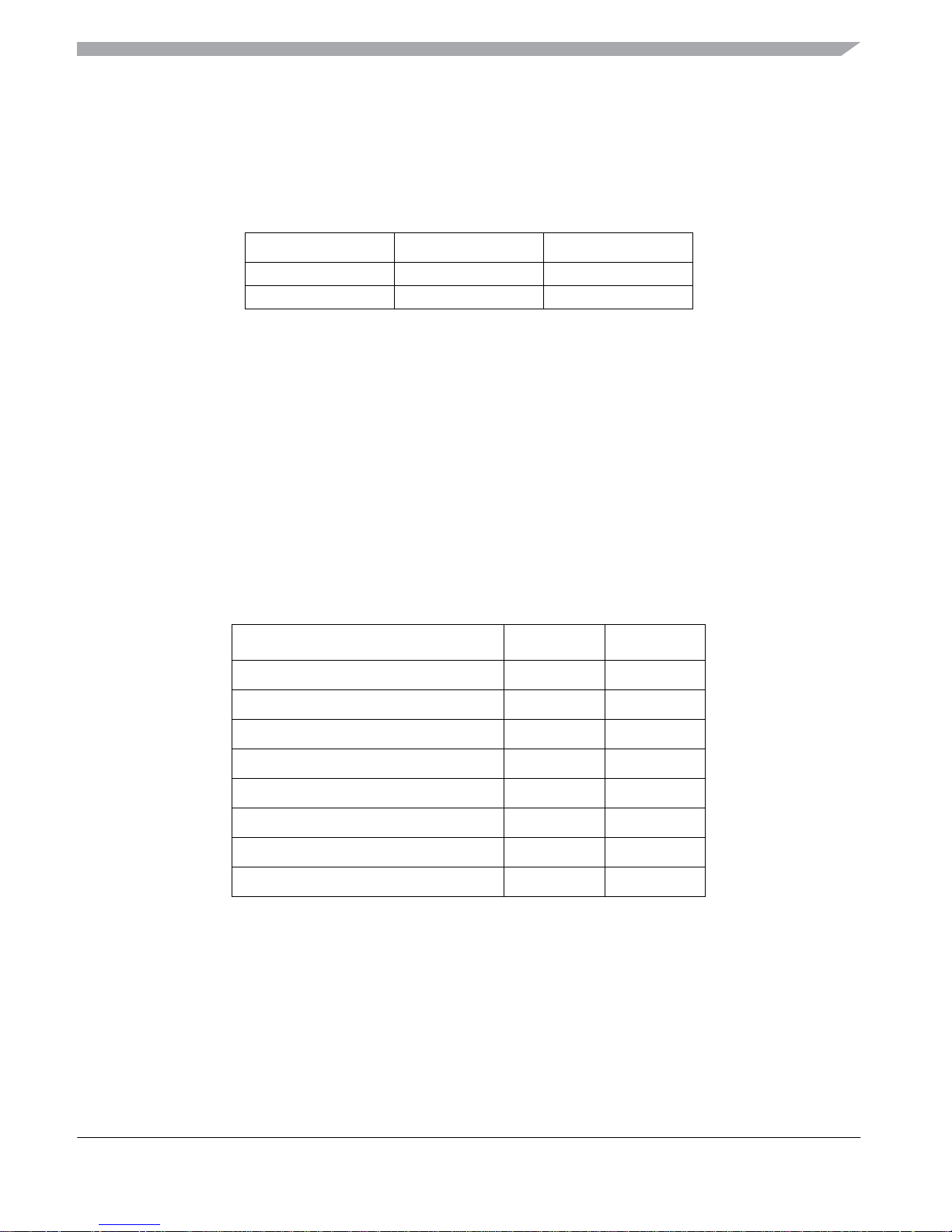
Device Overview MC9S12VR-Family
MC9S12VR Family Reference Manual, Rev. 2.2
Freescale Semiconductor 31
Preliminary - Subject to Change Without Notice
1.6.1 Part ID Assignments
The part ID is located in two 8-bit registers PARTIDH and PARTIDL (addresses 0x001A and 0x001B).
The read-only value is a unique part ID for each revision of the chip. Table 1-4 shows the assigned part ID
number and mask set number.
1.7 Signal Description and Device Pinouts
This section describes signals that connect off-chip. It includes a pinout diagram, a table of signal
properties, and detailed discussion of signals. It is built from the signal description sections of the
individual IP blocks on the device.
1.7.1 Pin Assignment Overview
Table 1-5 provides a summary of which ports are available for 32-pin and 48-pin package option.
NOTE
To avoid current drawn from floating inputs, all non-bonded pins should be
configured as output or configured as input with a pull up or pull down
device enabled
Table 1-4. Assigned Part ID Numbers
Device Mask Set Number Part ID
MC9S12VR48 N05E $3281
MC9S12VR64 N05E $3281
Table 1-5. Port Availability by Package Option
Port 32 LQFP 48 LQFP
Port AD PAD[1:0] PAD[5:0]
Port E PE[1:0] PE[1:0]
Port P PP1,PP2 PP[5:0]
Port S PS[3:2] PS[5:0]
Port T PT[3:0] PT[3:0]
Port L PL[3:0] PL[3:0]
sum of ports 16 28
I/O power pairs VDDX/VSSX 1/1 2/2
Downloaded from Elcodis.com electronic components distributor
Page 32

Device Overview MC9S12VR-Family
MC9S12VR Family Reference Manual, Rev. 2.2
32 Freescale Semiconductor
Preliminary - Subject to Change Without Notice
1.7.2 Detailed Signal Descriptions
This section describes the signal properties.
1.7.2.1 RESET — External Reset Signal
The RESET signal is an active low bidirectional control signal. It acts as an input to initialize the MCU to
a known start-up state, and an output when an internal MCU function causes a reset. The
RESET pin has
an internal pull-up device.
1.7.2.2 TEST — Test Pin
This input only pin is reserved for factory test. This pin has an internal pull-down device.
NOTE
The TEST pin must be tied to ground in all applications.
1.7.2.3 BKGD / MODC — Background Debug and Mode Pin
The BKGD/MODC pin is used as a pseudo-open-drain pin for the background debug communication. It
is used as a MCU operating mode select pin during reset. The state of this pin is latched to the MODC bit
at the rising edge of
RESET. The BKGD pin has an internal pull-up device.
1.7.2.4 PAD[5:0] / KWAD[5:0] — Port AD Input Pins of ADC
PAD[5:0] are general-purpose input or output signals. The signals can be configured on per signal basis as
interrupt inputs with wake-up capability (KWAD[5:0]).These signals can have a pull-up or pull-down
device selected and enabled on per signal basis. Out of reset the pull devices are disabled.
1.7.2.5 PE[1:0] — Port E I/O Signals
PE[1:0] are general-purpose input or output signals. The signals can have pull-down device, enabled by a
single control bit for this signal group. Out of reset the pull-down devices are enabled.
1.7.2.6 PP[5:0] / KWP[5:0] — Port P I/O Signals
PP[5:0] are general-purpose input or output signals. The signals can be configured on per signal basis as
interrupt inputs with wake-up capability (KWP[5:0]). PP[2] has a high current drive strength and an
over-current interrupt feature. They can have a pull-up or pull-down device selected and enabled on per
signal basis. Out of reset the pull devices are disabled.
1.7.2.7 PS[5:0] — Port S I/O Signals
PS[5:0] are general-purpose input or output signals. They can have a pull-up or pull-down device selected
and enabled on per signal basis. Out of reset the pull-up devices are enabled.
Downloaded from Elcodis.com electronic components distributor
Page 33

Device Overview MC9S12VR-Family
MC9S12VR Family Reference Manual, Rev. 2.2
Freescale Semiconductor 33
Preliminary - Subject to Change Without Notice
1.7.2.8 PT[3:0] — Port T I/O Signals
PT[3:0] are general-purpose input or output signals. They can have a pull-up or pull-down device selected
and enabled on per signal basis. Out of reset the pull devices are disabled.
1.7.2.9 PL[3:0] / KWL[3:0] — Port L Input Signals
PL[3:0] are high voltage input ports. The signals can be configured on per signal basis as interrupt inputs
with wake-up capability (KWL[3:0]).
1.7.2.10 LIN — LIN Physical Layer
This pad is connected to the single-wire LIN data bus.
1.7.2.11 HS[1:0] — High-Side Drivers Output Signals
Outputs of the two high-side drivers intended to drive incandescent bulbs or LEDs.
1.7.2.12 LS[1:0] — Low-Side Drivers Output Signals
Outputs of the two low-side drivers intended to drive inductive loads (relays).
1.7.2.13 VSENSE — Voltage Sensor Input
This pin can be connected to the supply (Battery) line for voltage measurements. The voltage present at
this input is scaled down by an internal voltage divider, and can be routed to the internal ADC via an analog
multiplexer. The pin itself is protected against reverse battery connections. To protect the pin from external
fast transients an external resistor is needed.
1.7.2.14 AN[5:0] — ADC Input Signals
AN[5:0] are the analog inputs of the Analog-to-Digital Converter.
1.7.2.15 SPI Signals
1.7.2.15.1 SS Signal
This signal is associated with the slave select SS functionality of the serial peripheral interface SPI.
1.7.2.15.2 SCK Signal
This signal is associated with the serial clock SCK functionality of the serial peripheral interface SPI.
1.7.2.15.3 MISO Signal
This signal is associated with the MISO functionality of the serial peripheral interface SPI. This signal acts
as master input during master mode or as slave output during slave mode.
Downloaded from Elcodis.com electronic components distributor
Page 34

Device Overview MC9S12VR-Family
MC9S12VR Family Reference Manual, Rev. 2.2
34 Freescale Semiconductor
Preliminary - Subject to Change Without Notice
1.7.2.15.4 MOSI Signal
This signal is associated with the MOSI functionality of the serial peripheral interface SPI. This signal acts
as master output during master mode or as slave input during slave mode
1.7.2.16 LINPHY Signals
1.7.2.16.1 LPTXD Signal
This signal is the LINPHY transmit input. See Figure 2-22
1.7.2.16.2 LPRXD Signal
This signal is the LINPHY receive output. See Figure 2-22
1.7.2.17 SCI Signals
1.7.2.17.1 RXD[1:0] Signals
Those signals are associated with the receive functionality of the serial communication interfaces SCI1-0.
1.7.2.17.2 TXD[1:0] Signals
Those signals are associated with the transmit functionality of the serial communication interfaces SCI1-0.
1.7.2.18 PWM[7:0] Signals
The signals PWM[7:0] are associated with the PWM module outputs.
1.7.2.19 Internal Clock outputs
1.7.2.19.1 ECLK
This signal is associated with the output of the divided bus clock (ECLK).
NOTE
This feature is only intended for debug purposes at room temperature.
It must not be used for clocking external devices in an application.
1.7.2.20 ETRIG[1:0]
These signals are inputs to the Analog-to-Digital Converter. Their purpose is to trigger ADC conversions.
1.7.2.21 IOC[3:0] Signals
The signals IOC[3:0] are associated with the input capture or output compare functionality of the timer
(TIM) module.
Downloaded from Elcodis.com electronic components distributor
Page 35

Device Overview MC9S12VR-Family
MC9S12VR Family Reference Manual, Rev. 2.2
Freescale Semiconductor 35
Preliminary - Subject to Change Without Notice
1.7.3 Power Supply Pins
MC9S12VR-Family power and ground pins are described below. Because fast signal transitions place
high, short-duration current demands on the power supply, use bypass capacitors with high-frequency
characteristics and place them as close to the MCU as possible.
NOTE
All ground pins must be connected together in the application.
1.7.3.1 VDDX1, VDDX2, VSSX1,VSSX2 — Power Output Pins and Ground Pins
VDDX1 and VDDX2 are the 5V power supply output for the I/O drivers. This voltage is generated by the
on chip voltage regulator. Bypass requirements on VDDX1 and VDDX2 pins depend on how heavily the
MCU pins are loaded. All VDDX pins are connected together internally. All VSSX pins are connected
together internally.
NOTE
The high side driver ground pin VSSXHS mentioned in Chapter 13,
“High-Side Drivers - HSDRV (S12HSDRV1) is internally connected to
VSSX2 ground pin.
NOTE
Not all power and ground pins are available on all packages. Refer to pinout
section for further details.
1.7.3.2 VDDA, VSSA — Power Supply Pins for ADC
These are the power supply and ground input pins for the analog-to-digital converter and the voltage
regulator.
NOTE
The reference voltages VRH and VRL mentioned in Appendix C, “ATD
Electrical Specifications are internally connected to VDDA and VSSA.
1.7.3.3 VSS — Core Ground Pin
The voltage supply of nominally 1.8V is generated by the internal voltage regulator. The return current
path is through the VSS pin.
1.7.3.4 LGND — LINPHY Ground Pin
LGND is the the ground pin for the LIN physical layer LINPHY.
1.7.3.5 LSGND — Ground Pin for Low-Side Drivers
LSGND is the shared ground pin for the low-side drivers.
Downloaded from Elcodis.com electronic components distributor
Page 36
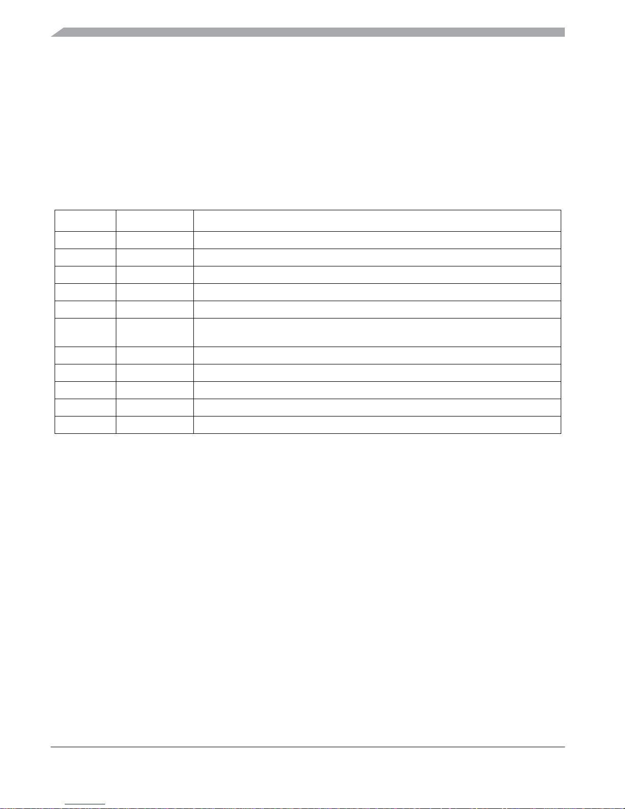
Device Overview MC9S12VR-Family
MC9S12VR Family Reference Manual, Rev. 2.2
36 Freescale Semiconductor
Preliminary - Subject to Change Without Notice
1.7.3.6 VSUP — Voltage Supply Pin for Voltage Regulator
VSUP is the 12V/18V shared supply voltage pin for the on chip voltage regulator.
1.7.3.7 VSUPHS — Voltage Supply Pin for High-Side Drivers
VSUPHS is the 12V/18V shared supply voltage pin for the high-side drivers.
1.7.3.8 Power and Ground Connection Summary
Table 1-6. Power and Ground Connection Summary
1.8 Device Pinouts
MC9S12VR-Familyis available in 48-pin package and 32-pin package. Signals in parentheses in
Figure 1-3. and Figure 1-4. denote alternative module routing options.
Mnemonic Nominal Voltage Description
VSS 0V Ground pin for 1.8V core supply voltage generated by on chip voltage regulator
VDDX1 5.0 V 5V power supply output for I/O drivers generated by on chip voltage regulator
VSSX1 0V Ground pin for I/O drivers
VDDX2 5.0 V 5V power supply output for I/O drivers generated by on chip voltage regulator
VSSX2 0V Ground pin for I/O drivers
VDDA 5.0 V External power supply for the analog-to-digital converter and for the reference circuit of the
internal voltage regulator
VSSA 0V Ground pin for VDDA analog supply
LGND 0V Ground pin for LIN physical
LSGND 0V Ground pin for low-side driver
VSUP 12V/18V External power supply for voltage regulator
VSUPHS 12V/18V External power supply for high-side driver
Downloaded from Elcodis.com electronic components distributor
Page 37
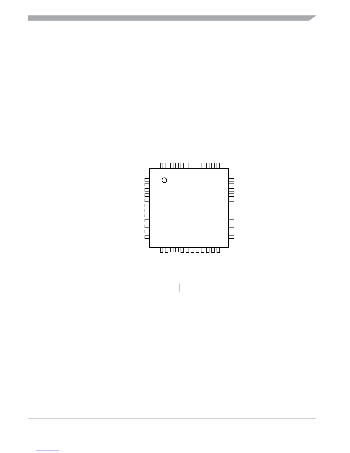
Device Overview MC9S12VR-Family
MC9S12VR Family Reference Manual, Rev. 2.2
Freescale Semiconductor 37
Preliminary - Subject to Change Without Notice
1.8.1 Pinout 48-pin LQFP
Figure 1-3. MC9S12VR 48-pin LQFP pinout
1
2
3
4
5
6
7
8
9
10
11
12
1314151617181920212223
24
36
35
34
33
32
31
30
29
28
27
26
25
4847464544434241403938
37
MC9S12VR
48-pin LQFP
Pin out is subject to
change!
PAD4 / KWAD4 / AN4
PAD5 / KWAD5 / AN5
PL3 / HVI3 / KWL3
PL2 / HVI2 / KWL2
PL1 / HVI1 / KWL1
PL0 / HVI0 / KWL0
VSENSE
HS1 / (OC3) / (PWM1) / (PWM4)
VSSX2
HS0 / (OC2) / (PWM3)
VSUPHS
VSUP
TEST
RESET
PWM3 / KWP3 / PP3
PWM4 / KWP4 / PP4
PWM5 / IRQ / KWP5 / PP5
VSS
EXTAL / PE0
XTAL / PE1
VDDX2
PWM0 / ETRIG0 / KWP0 / PP0
XIRQ / PWM1 / ETRIG1 / KWP1 / PP1
PWM2 / EVDD / KWP2 / PP2
LGND
LIN
(PWM5) / (PWM6) / (OC0) / LS0
LSGND
(PWM7) / (OC1) / LS1
VSSX1
VDDX1
MISO / (RXD1) / (PWM4) / (ETRIG0) / PS2
ECLK / MOSI / (TXD1) / (PWM5) / (ETRIG1) / PS3
SCK / PS4
SS / PS5
MODC / BKGD
PS1 / (TXD0) / (LPDR1) / TXD1
PS0 / (RXD0) / RXD1
PT3 / IOC3 / (LPTXD) / (SS)
PT2 / IOC2 / (LPRXD) / (SCK)
PT1 / IOC1 / PWM7 / (TXD0) / (LPDR)
PT0 / IOC0 / PWM6 / (RXD0)
PAD0 / KWAD0 / AN0
PAD1 / KWAD1 / AN1
PAD2 / KWAD2 / AN2
PAD3 / KWAD3 / AN3
VDDA
VSSA
Downloaded from Elcodis.com electronic components distributor
Page 38
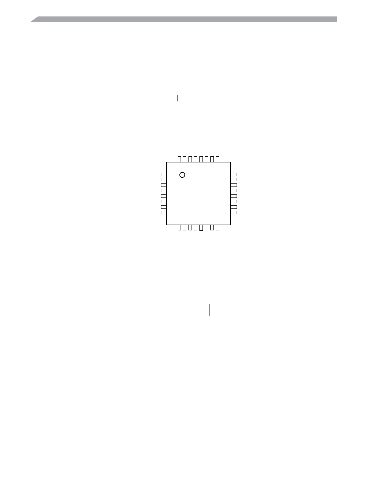
Device Overview MC9S12VR-Family
MC9S12VR Family Reference Manual, Rev. 2.2
38 Freescale Semiconductor
Preliminary - Subject to Change Without Notice
1.8.2 Pinout 32-pin LQFP
Figure 1-4. MC9S12VR 32-pin LQFP pinout
1
2
3
4
5
6
7
8
9
10111213141516
24
23
22
21
20
19
18
17
MC9S12VR
32-pin LQFP
Pin out is
subject to
change!
PL3 / HVI3 / KWL3
PL2 / HVI2 / KWL2
PL1 / HVI1 / KWL1
PL0 / HVI0 / KWL0
VSENSE
VSSX2
HS0 / (OC2) / (PWM3)
VSUP
TEST
RESET
VSS
EXTAL / PE0
XTAL / PE1
VDDX2
XIRQ / PWM1 / ETRIG1 / KWP1 / PP1
PWM2 / EVDD / KWP2 / PP2
LGND
LIN
(PWM5) / (PWM6) / (OC0) / LS0
LSGND
(PWM3) / (PWM0) / (OC1) / LS1
MISO / (RXD1) / (PWM4) / (ETRIG0) / PS2
ECLK / MOSI / (TXD1) / (PWM5) / (ETRIG1) / PS3
MODC / BKGD
PT3 / IOC3 / (LPTXD) / (SS)
PT2 / IOC2 / (LPRXD) / (SCK)
PT1 / IOC1 / PWM7 / (TXD0) / (LPDR1)
PT0 / IOC0 / PWM6 / (RXD0)
PAD0 / KWAD0 / AN0
PAD1 / KWAD1 / AN1
VDDA
VSSA
32313029282726
25
Downloaded from Elcodis.com electronic components distributor
Page 39
Device Overview MC9S12VR-Family
MC9S12VR Family Reference Manual, Rev. 2.2
Freescale Semiconductor 39
Preliminary - Subject to Change Without Notice
Table 1-7. Pin Summary
Package Function
Power
Supply
Internal Pull
Resistor
48
LQ
FP
32
LQ
FP
Pin
1th
Func.
2nd
Func.
3rd
Func.
4th
Func.
5th
Func.
CTRL
Reset
State
1 1 LGND —————— — —
22LIN—————— — —
3 3 LS0 OC0
1
PWM5 PWM6 — — — — —
4 4 LSGND —————— — —
5 5 LS1 OC1 PWM7 — — — — — —
6 — VSSX1 —————— — —
7 — VDDX1 —————V
DDX
——
8 6 PS2 ETRIG0 PWM4 RXD1 MISO — V
DDX
PERS/PPSS Up
9 7 PS3 ETRIG1 PWM5 TXD1 MOSI ECLK V
DDX
PERS/PPSS Up
10—PS4SCK————V
DDX
PERS/PPSS Up
11 — PS5
SS————V
DDX
PERS/PPSS Up
12 8 BKGD MODC ————V
DDX
PUCR/BKPUE Up
13 9 TEST —————N.A
RESET pin Down
14 10
RESET —————V
DDX
TEST pin Up
15 — PP3 KWP3 PWM3 — — — V
DDX
PERP/PPSP Disabled
16 — PP4 KWP4 PWM4 — — — V
DDX
PERP/PPSP Disabled
17 — PP5 KWP5 PWM5
IRQ — — V
DDX
PERP/PPSP Disabled
18 11 VSS ——————— —
1912PE0EXTAL————V
DDX
PUCR/PUPEE Up
2013PE1XTAL————V
DDX
PUCR/PUPEE Up
21 14 VDDX2 —————— — —
22 — PP0 KWP0 ETRIG0 PWM0 — — V
DDX
PERP/PPSP Disabled
23 15 PP1 KWP1 ETRIG1 PWM1
XIRQ — V
DDX
PERP/PPSP Disabled
24 16 PP2 KWP2 EVDD PWM2 — — V
DDX
PERP/PPSP Disabled
25 17 VSUP —————— — —
26 — VSUPHS — ————— — —
27 18 HS0 OC2 PWM3 — — — V
SUPH
S
——
Downloaded from Elcodis.com electronic components distributor
Page 40
Device Overview MC9S12VR-Family
MC9S12VR Family Reference Manual, Rev. 2.2
40 Freescale Semiconductor
Preliminary - Subject to Change Without Notice
28 19 VSSX2 —————— — —
29 — HS1 OC3 PWM1 PWM4 — — V
SUPH
S
——
30 20 VSENSE —————— — —
31 21 PL0 HVI0 KWL0 — — — V
DDX
——
32 22 PL1 HVI1 KWL1 — — — V
DDX
——
33 23 PL2 HVI2 KWL2 — — — V
DDX
——
34 24 PL3 HVI3 KWL3 — — — V
DDX
——
35 — PAD5 KWAD5 AN5 — — — V
DDA
PER1AD/
PPS1AD
Disabled
36 — PAD4 KWAD4 AN4 — — — V
DDA
PER1AD/
PPS1AD
Disabled
37 25 VSSA —————— — —
3826VDDA—————— — —
39 — PAD3 KWAD3 AN3 — — — V
DDA
PER1AD/
PPS1AD
Disabled
40 — PAD2 KWAD2 AN2 — — — V
DDA
PER1AD/
PPS1AD
Disabled
41 27 PAD1 KWAD1 AN1 — — — V
DDA
PER1AD/
PPS1AD
Disabled
42 28 PAD0 KWAD0 AN0 — — — V
DDA
PER1AD/
PPS1AD
Disabled
43 29 PT0 IOC0 PWM6 RXD0 — — V
DDX
PERT/PPST Disabled
44 30 PT1 IOC1 PWM7 TXD0 LPDR1 — V
DDX
PERT/PPST Disabled
45 31 PT2 IOC2 LPRXD SCK — — V
DDX
PERT/PPST Disabled
46 32 PT3 IOC3 LPTXD
SS — — V
DDX
PERT/PPST Disabled
47 — PS0 RXD0 RXD1 — — — V
DDX
PERS/PPSS Up
48 — PS1 TXD0 LPDR1 TXD1 — — V
DDX
PERS/PPSS Up
1
Timer Output Compare Channel
Package Function
Power
Supply
Internal Pull
Resistor
48
LQ
FP
32
LQ
FP
Pin
1th
Func.
2nd
Func.
3rd
Func.
4th
Func.
5th
Func.
CTRL
Reset
State
Downloaded from Elcodis.com electronic components distributor
Page 41

Device Overview MC9S12VR-Family
MC9S12VR Family Reference Manual, Rev. 2.2
Freescale Semiconductor 41
Preliminary - Subject to Change Without Notice
1.9 Modes of Operation
The MCU can operate in different modes. These are described in 1.9.1 Chip Configuration Summary.
The MCU can operate in different power modes to facilitate power saving when full system performance
is not required. These are described in 1.9.2 Low Power Operation.
Some modules feature a software programmable option to freeze the module status whilst the background
debug module is active to facilitate debugging.
1.9.1 Chip Configuration Summary
The different modes and the security state of the MCU affect the debug features (enabled or disabled).
The operating mode out of reset is determined by the state of the MODC signal during reset (see
Table 1-8). The MODC bit in the MODE register shows the current operating mode and provides limited
mode switching during operation. The state of the MODC signal is latched into this bit on the rising edge
of
RESET.
1.9.1.1 Normal Single-Chip Mode
This mode is intended for normal device operation. The opcode from the on-chip memory is being
executed after reset (requires the reset vector to be programmed correctly). The processor program is
executed from internal memory.
1.9.1.2 Special Single-Chip Mode
This mode is used for debugging single-chip operation, boot-strapping, or security related operations. The
background debug module BDM is active in this mode. The CPU executes a monitor program located in
an on-chip ROM. BDM firmware waits for additional serial commands through the BKGD pin.
1.9.2 Low Power Operation
The MC9S12VR-Family has two dynamic-power modes (run and wait) and two static low-power modes
stop and pseudo stop). For a detailed description refer to Section Chapter 4 Clock, Reset and Power
Management (S12CPMU_UHV).
• Dynamic power mode: Run
— Run mode is the main full performance operating mode with the entire device clocked. The user
can configure the device operating speed through selection of the clock source and the phase
locked loop (PLL) frequency. To save power, unused peripherals must not be enabled.
Table 1-8. Chip Modes
Chip Modes MODC
Normal single chip 1
Special single chip 0
Downloaded from Elcodis.com electronic components distributor
Page 42
Device Overview MC9S12VR-Family
MC9S12VR Family Reference Manual, Rev. 2.2
42 Freescale Semiconductor
Preliminary - Subject to Change Without Notice
• Dynamic power mode: Wait
— This mode is entered when the CPU executes the WAI instruction. In this mode the CPU will
not execute instructions. The internal CPU clock is switched off. All peripherals can be active
in system wait mode. For further power consumption the peripherals can individually turn off
their local clocks. Asserting
RESET, XIRQ, IRQ, or any other interrupt that is not masked ends
system wait mode.
• Static power mode Pseudo-stop:
— In this mode the system clocks are stopped but the oscillator is still running and the real time
interrupt (RTI) and watchdog (COP), Autonomous Periodic Interrupt (API) and ATD modules
may be enabled. Other peripherals are turned off. This mode consumes more current than
system STOP mode but, as the oscillator continues to run, the full speed wake up time from this
mode is significantly shorter.
• Static power mode: Stop
— The oscillator is stopped in this mode. By default, all clocks are switched off and all counters
and dividers remain frozen. The autonomous periodic interrupt (API), ATD, key wake-up and
the LIN physical layer transceiver modules may be enabled to wake the device.
1.10 Security
The MCU security mechanism prevents unauthorized access to the Flash memory. Refer to Section 5.4.1
Security and Section 17.5 Security.
1.11 Resets and Interrupts
Consult the S12 CPU manual and the S12SINT section for information on exception processing.
1.11.1 Resets
Table 1-9. lists all Reset sources and the vector locations. Resets are explained in detail in the Chapter 4,
“Clock, Reset and Power Management (S12CPMU_UHV)”.
Table 1-9. Reset Sources and Vector Locations
Vector Address Reset Source
CCR
Mask
Local Enable
$FFFE Power-On Reset (POR) None None
$FFFE Low Voltage Reset (LVR) None None
$FFFE External pin RESET None None
$FFFE Illegal Address Reset None None
$FFFC Clock monitor reset None OSCE Bit in CPMUOSC register
Downloaded from Elcodis.com electronic components distributor
Page 43
Device Overview MC9S12VR-Family
MC9S12VR Family Reference Manual, Rev. 2.2
Freescale Semiconductor 43
Preliminary - Subject to Change Without Notice
1.11.2 Interrupt Vectors
Table 1-10 lists all interrupt sources and vectors in the default order of priority. The interrupt module (see
Chapter 7, “Interrupt Module (S12SINTV1)”) provides an interrupt vector base register (IVBR) to relocate
the vectors.
$FFFA COP watchdog reset None CR[2:0] in CPMUCOP register
Table 1-10. Interrupt Vector Locations (Sheet 1 of 2)
Vector Address
1
Interrupt Source
CCR
Mask
Local Enable
Wake up
from STOP
Wake up
from WAIT
Vector base + $F8 Unimplemented instruction trap None None - -
Vector base+ $F6 SWI None None - -
Vector base+ $F4 XIRQ X Bit None Yes Yes
Vector base+ $F2
IRQ I bit IRQCR (IRQEN) Yes Yes
Vector base+ $F0 RTI time-out interrupt I bit CPMUINT (RTIE)
4.6 Interrupts
Vector base+ $EE TIM timer channel 0 I bit TIE (C0I) No Yes
Vector base + $EC TIM timer channel 1 I bit TIE (C1I) No Yes
Vector base+ $EA TIM timer channel 2 I bit TIE (C2I) No Yes
Vector base+ $E8 TIM timer channel 3 I bit TIE (C3I) No Yes
Vector base+ $E6
to
Vector base + $E0
Reserved
Vector base+ $DE TIM timer overflow I bit TSCR2(TOF) No Yes
Vector base+ $DC
to
Vector base + $DA
Reserved
Vector base + $D8 SPI I bit SPICR1 (SPIE, SPTIE) No Yes
Vector base+ $D6 SCI0 I bit SCI0CR2
(TIE, TCIE, RIE, ILIE)
Ye s Ye s
Vector base + $D4 SCI1 I bit SCI1CR2
(TIE, TCIE, RIE, ILIE)
Ye s Ye s
Vector base + $D2 ADC I bit ATDCTL2 (ASCIE) No Yes
Vector base + $D0 Reserved
Vector base + $CE Port L I bit PIEL (PIEL3-PIEL0) Yes Yes
Vector Address Reset Source
CCR
Mask
Local Enable
Downloaded from Elcodis.com electronic components distributor
Page 44
Device Overview MC9S12VR-Family
MC9S12VR Family Reference Manual, Rev. 2.2
44 Freescale Semiconductor
Preliminary - Subject to Change Without Notice
1.11.3 Effects of Reset
When a reset occurs, MCU registers and control bits are initialized. Refer to the respective block sections
for register reset states.
Vector base + $CC
to
Vector base + $CA
Reserved
Vector base + $C8
Oscillator status interrupt I bit
CPMUINT (OSCIE)
No Yes
Vector base + $C6 PLL lock interrupt I bit CPMUINT (LOCKIE) No Yes
Vector base + $C4
to
Vector base + $BC
Reserved
Vector base + $BA FLASH error I bit FERCNFG (SFDIE, DFDIE) No No
Vector base + $B8 FLASH command I bit FCNFG (CCIE) No Yes
Vector base + $B6
to
Vector base + $B0
Reserved
Vector base + $AE HSDRV over-current interrupt I bit HSIE (HSERR)
No
Ye s
Vector base + $AC LSDRV over-current interrupt I bit LSIE (LSERR) No Yes
Vector base + $AA LINPHY over-current interrupt I bit LPIE (LPERR) Yes Yes
Vector base + $A8 BATS low & high battery voltage
interrupt
I bit BATIE (BVHIE,BVLIE) No Yes
Vector base + $A6
to
Vector base + $90
Reserved
Vector base + $8E Port P interrupt I bit PIEP (PIEP5-PIEP3,
PIEP1-PIEP0)
Ye s Ye s
Vector base+ $8C Port P2 (EVDD Hall Sensor Supply)
over-current interrupt
I bit PIEP (OCIE) No Yes
Vector base + $8A Low-voltage interrupt (LVI) I bit CPMUCTRL (LVIE) No Yes
Vector base + $88 Autonomous periodical interrupt
(API)
I bit
CPMUAPICTRL (APIE)
Ye s Ye s
Vector base + $86 High temperature interrupt I bit CPMUHTCTL(HTIE) Yes Yes
Vector base + $84 ADC compare interrupt I bit ATDCTL2 (ACMPIE) No Yes
Vector base + $82 Port AD interrupt I bit PIE1AD(PIE1AD5-PIE1AD0) Yes Yes
Vector base + $80 Spurious interrupt — None - -
1
16 bits vector address based
Table 1-10. Interrupt Vector Locations (Sheet 2 of 2)
Vector Address
1
Interrupt Source
CCR
Mask
Local Enable
Wake up
from STOP
Wake up
from WAIT
Downloaded from Elcodis.com electronic components distributor
Page 45
Device Overview MC9S12VR-Family
MC9S12VR Family Reference Manual, Rev. 2.2
Freescale Semiconductor 45
Preliminary - Subject to Change Without Notice
On each reset, the Flash module executes a reset sequence to load Flash configuration registers.
1.11.3.1 Flash Configuration Reset Sequence Phase
On each reset, the Flash module will hold CPU activity while loading Flash module registers from the
Flash memory. If double faults are detected in the reset phase, Flash module protection and security may
be active on leaving reset. This is explained in more detail in the Flash module Section 17.1,
“Introduction”.
1.11.3.2 Reset While Flash Command Active
If a reset occurs while any Flash command is in progress, that command will be immediately aborted. The
state of the word being programmed or the sector/block being erased is not guaranteed.
1.11.3.3 I/O Pins
Refer to the PIM section for reset configurations of all peripheral module ports.
1.11.3.4 RAM
The RAM arrays are not initialized out of reset.
1.12 API external clock output (API_EXTCLK)
The API_EXTCLK option which is described 4.3.2.15 Autonomous Periodical Interrupt Control Register
(CPMUAPICTL) is not available on S12VR-Family.
1.13 COP Configuration
The COP time-out rate bits CR[2:0] and the WCOP bit in the CPMUCOP register at address 0x003C are
loaded from the Flash configuration field byte at global address 0x3_FF0E during the reset sequence. See
Table 1-11 and Table 1-12 for coding
Table 1-11. Initial COP Rate Configuration
NV[2:0] in
FOPT Register
CR[2:0] in
COPCTL Register
000 111
001 110
010 101
011 100
100 011
101 010
110 001
111 000
Downloaded from Elcodis.com electronic components distributor
Page 46
Device Overview MC9S12VR-Family
MC9S12VR Family Reference Manual, Rev. 2.2
46 Freescale Semiconductor
Preliminary - Subject to Change Without Notice
1.14 ADC External Trigger Input Connection
The ADC module includes external trigger inputs ETRIG0, ETRIG1, ETRIG2, and ETRIG3. The external
trigger allows the user to synchronize ADC conversion to external trigger events. ETRIG0 is connected to
PP0 / PWM0 and ETRIG1 is connected to PP1 / PWM1. ETRIG2 and ETRIG3 are not used .ETRIG0 can
be routed to PS2 and ETRIG1 can be routed to PS3.
1.15 ADC Special Conversion Channels
Whenever the ADC’s Special Channel Conversion Bit (SC) in 8.3.2.6 ATD Control Register 5 (ATDCTL5)
is set, it is capable of running conversion on a number of internal channels. Table 1-13 lists the internal
sources which are connected to these special conversion channels.
Table 1-12. Initial WCOP Configuration
NV[3] in
FOPT Register
WCOP in
COPCTL Register
10
01
Table 1-13. Usage of ADC Special Conversion Channels
ATDCTL5 Register Bits Usage
SC CD CC CB CA ADC Channel
1 0 0 0 1 Internal_7 Bandgap Voltage V
BG
or Chip temperature
sensor V
HT
see 4.3.2.13 High Temperature
Control Register (CPMUHTCTL)
1 0 0 1 0 Internal_0 Flash Supply Voltage VDDF
1 0 0 1 1 Internal_1 LINPHY temperature sensor
1 1 0 1 0 Internal_4 V
SENSE
or V
SUP
selectable in BATS module
see 16.1.1 Features
1 1 0 1 1 Internal_5 High voltage inputs Port L see 2.3.34 Port L
Analog Access Register (PTAL)
Downloaded from Elcodis.com electronic components distributor
Page 47

MC9S12VR Family Reference Manual, Rev. 2.2
Freescale Semiconductor 47
Preliminary - Subject to Change Without Notice
Chapter 2
Port Integration Module (S12VRPIMV2)
Table 2-1. Revision History
2.1 Introduction
2.1.1 Overview
The S12VR port integration module (PIM) establishes the interface between the peripheral modules and
the I/O pins for all ports. It controls the electrical pin properties as well as the signal prioritization and
multiplexing on shared pins.
This section covers:
• 2-pin port E associated with the external oscillator
• 4-pin port T associated with 4 TIM channels and 2 PWM channels
• 6-pin port S associated with 2 SCI and 1 SPI
• 6-pin port P with pin interrupts and wakeup function; associated with
—
IRQ, XIRQ interrupt inputs
Rev. No.
(Item No.)
Date
(Submitted By)
Sections
Affected
Substantial Change(s)
V02.00 05 Apr 2011 • Changed DDRL to DIENL (digital input buffer enable) with inverse
functionality
• Renamed routing registers to MODRR
• Added 6 PWM channels (ports P and T) Changed PWM routing options to
HS[1:0] and LS[1:0]
• Added PTADIRL and PTABYP bits to support ADC direct input Changed
PWM and ETRIG routing assignments on port S
• Corrected reduced drive ratio on PP2
• Added HVI open input detection (moved PIMTEST[PLTEN] to
PTAL[PTTEL] and PIMTEST[PLTPU] to PTAL[PTPSL])
• Added application section for HVI open input detection
• Revised port L HVI diagram for HVI open input detection
•
V02.01 07 Apr 2011 • Minor corrections after review
V02.02 11 Apr 2011 • Added stop mode condition to PTTEL and PTPSL
• Minor corrections after review
V02.03 18 Apr 2011 • Minor corrections after review
Downloaded from Elcodis.com electronic components distributor
Page 48

Port Integration Module (S12VRPIMV2)
MC9S12VR Family Reference Manual, Rev. 2.2
48 Freescale Semiconductor
Preliminary - Subject to Change Without Notice
— Six PWM channels with two of those capable of driving up to 10 mA
— One output with over-current protection and interrupt capable of supplying up to 20 mA to
external devices such as Hall sensors
• 6-pin port AD with pin interrupts and wakeup function; associated with 6 ADC channels
• 4-pin port L with pin interrupts and wakeup function; associated with 4 high-voltage inputs for
digital or analog use with optional voltage divider bypass and open input detection
Most I/O pins can be configured by register bits to select data direction and to enable and select pullup or
pulldown devices.
2.1.2 Features
The PIM includes these distinctive registers:
• Data registers and data direction registers for Ports E, T, S, P and AD when used as general-purpose
I/O
• Control registers to enable/disable pull devices and select pullups/pulldowns on Ports T, S, P, AD
on per-pin basis
• Single control register to enable/disable pullups on Port E on per-port basis and on BKGD pin
• Control registers to enable/disable open-drain (wired-or) mode on Port S
• Control register to enable/disable reduced output drive on Port P high-current pins
• Interrupt flag register for pin interrupts on Port P, L and AD
• Control register to configure
IRQ pin operation
• Control register to enable ECLK clock output
• Routing registers to support module port relocation and control internal module routings:
— PWM and ETRIG to alternative pins
— SPI
SS and SCK to alternative pins
— SCI1 to alternative pins
— HSDRV and LSDRV control selection from PWM, TIM or related register bit
— Various SCI0-LINPHY routing options supporting standalone use and conformance testing
— Optional LINPHY to TIM link
— Optional HVI to ADC link
A standard port pin has the following minimum features:
• Input/output selection
• 5 V output drive
• 5 V digital and analog input
• Input with selectable pullup or pulldown device
Optional features supported on dedicated pins:
• Two selectable output drive strengths
• Open drain for wired-or connections
Downloaded from Elcodis.com electronic components distributor
Page 49
Port Integration Module (S12VRPIMV2)
MC9S12VR Family Reference Manual, Rev. 2.2
Freescale Semiconductor 49
Preliminary - Subject to Change Without Notice
• Interrupt input with glitch filtering
• High-voltage input
• 10 mA high-current output
• 20 mA high-current output with over-current protection for use as Hall sensor supply
2.2 External Signal Description
This section lists and describes the signals that do connect off-chip.
Table 2-2 shows all the pins and their functions that are controlled by the PIM. Routing options are denoted
in parenthesis.
NOTE
If there is more than one function associated with a pin, the
output priority
is indicated by the position in the table from top (highest priority) to bottom
(lowest priority).
Table 2-2. Pin Functions and Priorities
Port Pin Name
Pin Function
& Priority
1
I/O Description
Pin Function
after Reset
- BKGD MODC
2
I MODC input during RESET BKGD
BKGD I/O BDM communication pin
E PE1 XTAL - CPMU OSC signal GPIO
PTE[1] I/O General-purpose
PE0 EXTAL - CPMU OSC signal
PTE[0] I/O General-purpose
T PT3 (
SS) I/O SPI slave select GPIO
(LPTXD) I LINPHY transmit pin
IOC3 I/O TIM channel 3
PTT[3] I/O General-purpose
PT2 (SCK) I/O SPI serial clock
(LPRXD) O LINPHY receive pin
IOC2 I/O TIM channel 2
PTT[2] I/O General-purpose
PT1 (LPDR1) O LINPHY register LPDR[LPDR1]
(TXD0) I/O Serial Communication Interface 0 transmit pin
PWM7 O Pulse Width Modulator channel 7
IOC1 I/O TIM channel 1
PTT[1] I/O General-purpose
PT0 (RXD0) I Serial Communication Interface 0 receive pin
PWM6 O Pulse Width Modulator channel 6
IOC0 I/O TIM channel 0
PTT[0] I/O General-purpose
Downloaded from Elcodis.com electronic components distributor
Page 50
Port Integration Module (S12VRPIMV2)
MC9S12VR Family Reference Manual, Rev. 2.2
50 Freescale Semiconductor
Preliminary - Subject to Change Without Notice
S PS5
SS I/O SPI slave select GPIO
PTS[5] I/O General-purpose
PS4 SCK I/O SPI serial clock
PTS[4] I/O General-purpose
PS3 ECLK O Free running clock
MOSI I/O SPI master out / slave in
(TXD1) I/O Serial Communication Interface 1 transmit pin
(PWM5) O Pulse Width Modulator channel 5
(ETRIG1) I ADC external trigger input
PTS[3] I/O General-purpose
PS2 MISO I/O SPI master in / slave out
(RXD1) I Serial Communication Interface 1 receive pin
(PWM4) O Pulse Width Modulator channel 4
(ETRIG0) I ADC external trigger input
PTS[2] I/O General-purpose
PS1 TXD1 I/O Serial Communication Interface 1 transmit pin
(LPDR1) O LINPHY register LPDR[LPDR1]
(TXD0) I/O Serial Communication Interface 0 transmit pin
PTS[1] I/O General-purpose
PS0 RXD1 I Serial Communication Interface 1 receive pin
(RXD0) I Serial Communication Interface 0 receive pin
PTS[0] I/O General-purpose
Port Pin Name
Pin Function
& Priority
1
I/O Description
Pin Function
after Reset
Downloaded from Elcodis.com electronic components distributor
Page 51
Port Integration Module (S12VRPIMV2)
MC9S12VR Family Reference Manual, Rev. 2.2
Freescale Semiconductor 51
Preliminary - Subject to Change Without Notice
2.3 Memory Map and Register Definition
This section provides a detailed description of all PIM registers.
P PP5 IRQ I Maskable level- or falling edge-sensitive interrupt GPIO
PWM5 O Pulse Width Modulator channel 5
ETRIG1 I ADC external trigger input
PTP[5]/
KWP[5]
I/O General-purpose; with pin interrupt and wakeup
PP4 PWM4 O Pulse Width Modulator channel 4
ETRIG0 I ADC external trigger input
PTP[4]/
KWP[4]
I/O General-purpose; with pin interrupt and wakeup
PP3 PWM3 O Pulse Width Modulator channel 3
PTP[3]/
KWP[3]
I/O General-purpose; with pin interrupt and wakeup
PP2 PWM2 O Pulse Width Modulator channel 2
PTP[2]/
KWP[2]/
EVDD
I/O General-purpose; with pin interrupt and wakeup;
switchable external power supply output with over-current
interrupt; high-current capable (20 mA)
PP1
XIRQ I Non-maskable level-sensitive interrupt
PWM1 O Pulse Width Modulator channel 1; high-current capable (10 mA)
PTP[1]/
KWP[1]
I/O General-purpose; with interrupt and wakeup; high-current
capable (10 mA)
PP0 PWM0 O Pulse Width Modulator channel 0; high-current capable (10 mA)
PTP[0]/
KWP[0]
I/O General-purpose; with interrupt and wakeup; high-current
capable (10 mA)
L PL3-0 PTL[3:0]/
KWL[3:0]
I General-purpose high-voltage input (HVI); with interrupt and
wakeup; optional ADC link
GPI (HVI)
AD PAD5-0 AN[5:0] I ADC analog GPIO
PTAD[5:0]/
KWAD[5:0]
I/O General-purpose; with interrupt and wakeup
1
Signals in parentheses denote alternative module routing pins
2
Function active when RESET asserted
Port Pin Name
Pin Function
& Priority
1
I/O Description
Pin Function
after Reset
Downloaded from Elcodis.com electronic components distributor
Page 52
Port Integration Module (S12VRPIMV2)
MC9S12VR Family Reference Manual, Rev. 2.2
52 Freescale Semiconductor
Preliminary - Subject to Change Without Notice
2.3.1 Register Map
Global
Address
Register
Name
Bit 7 654321Bit 0
0x0000–
0x0007
Reserved
R00000000
W
0x0008 PORTE
R000000
PE1 PE0
W
0x0009 DDRE
R000000
DDRE1 DDRE0
W
0x000A–
0x000B
Non-PIM
Address Range
R
Non-PIM Address Range
W
0x000C PUCR
R0
BKPUE
0
PDPEE
0000
W
0x000D Reserved
R00000000
W
0x000E–
0x001B
Non-PIM
Address Range
R
Non-PIM Address Range
W
0x001C ECLKCTL
R
NECLK
0000000
W
0x001D PIMMISC
R
OCPE
0000000
W
0x001E IRQCR
R
IRQE IRQEN
000000
W
0x001F Reserved
R
Reserved Reserved Reserved Reserved Reserved Reserved Reserved Reserved
W
0x0020–
0x023F
Non-PIM
Address Range
R
Non-PIM Address Range
W
0x0240 PTT
R0000
PTT3 PTT2 PTT1 PTT0
W
0x0241 PTIT
R0000PTIT3 PTIT2 PTIT1 PTIT0
W
0x0242 DDRT
R0000
DDRT3 DDRT2 DDRT1 DDRT0
W
Downloaded from Elcodis.com electronic components distributor
Page 53
Port Integration Module (S12VRPIMV2)
MC9S12VR Family Reference Manual, Rev. 2.2
Freescale Semiconductor 53
Preliminary - Subject to Change Without Notice
0x0243 Reserved
R00000000
W
0x0244 PERT
R0000
PERT3 PERT2 PERT1 PERT0
W
0x0245 PPST
R0000
PPST3 PPST2 PPST1 PPST0
W
0x0246 MODRR0
R
MODRR07 MODRR06 MODRR05 MODRR04 MODRR03 MODRR02 MODRR01 MODRR00
W
0x0247 MODRR1
R0 0
MODRR15 MODRR14
0000
W
0x0248 PTS
R0 0
PTS5 PTS4 PTS3 PTS2 PTS1 PTS0
W
0x0249 PTIS
R 0 0 PTIS5 PTIS4 PTIS3 PTIS2 PTIS1 PTIS0
W
0x024A DDRS
R0 0
DDRS5 DDRS4 DDRS3 DDRS2 DDRS1 DDRS0
W
0x024B Reserved
R00000000
W
0x024C PERS
R0 0
PERS5 PERS4 PERS3 PERS2 PERS1 PERS0
W
0x024D PPSS
R0 0
PPSS5 PPSS4 PPSS3 PPSS2 PPSS1 PPSS0
W
0x024E WOMS
R0 0
WOMS5 WOMS4 WOMS3 WOMS2 WOMS1 WOMS0
W
0x024F MODRR2
R
MODRR27
0
MODRR25 MODRR24 MODRR23 MODRR22 MODRR21 MODRR20
W
0x0250–
0x0257
Reserved
R00000000
W
0x0258 PTP
R0 0
PTP5 PTP4 PTP3 PTP2 PTP1 PTP0
W
0x0259 PTIP
R 0 0 PTIP5 PTIP4 PTIP3 PTIP2 PTIP1 PTIP0
W
Global
Address
Register
Name
Bit 7 654321Bit 0
Downloaded from Elcodis.com electronic components distributor
Page 54
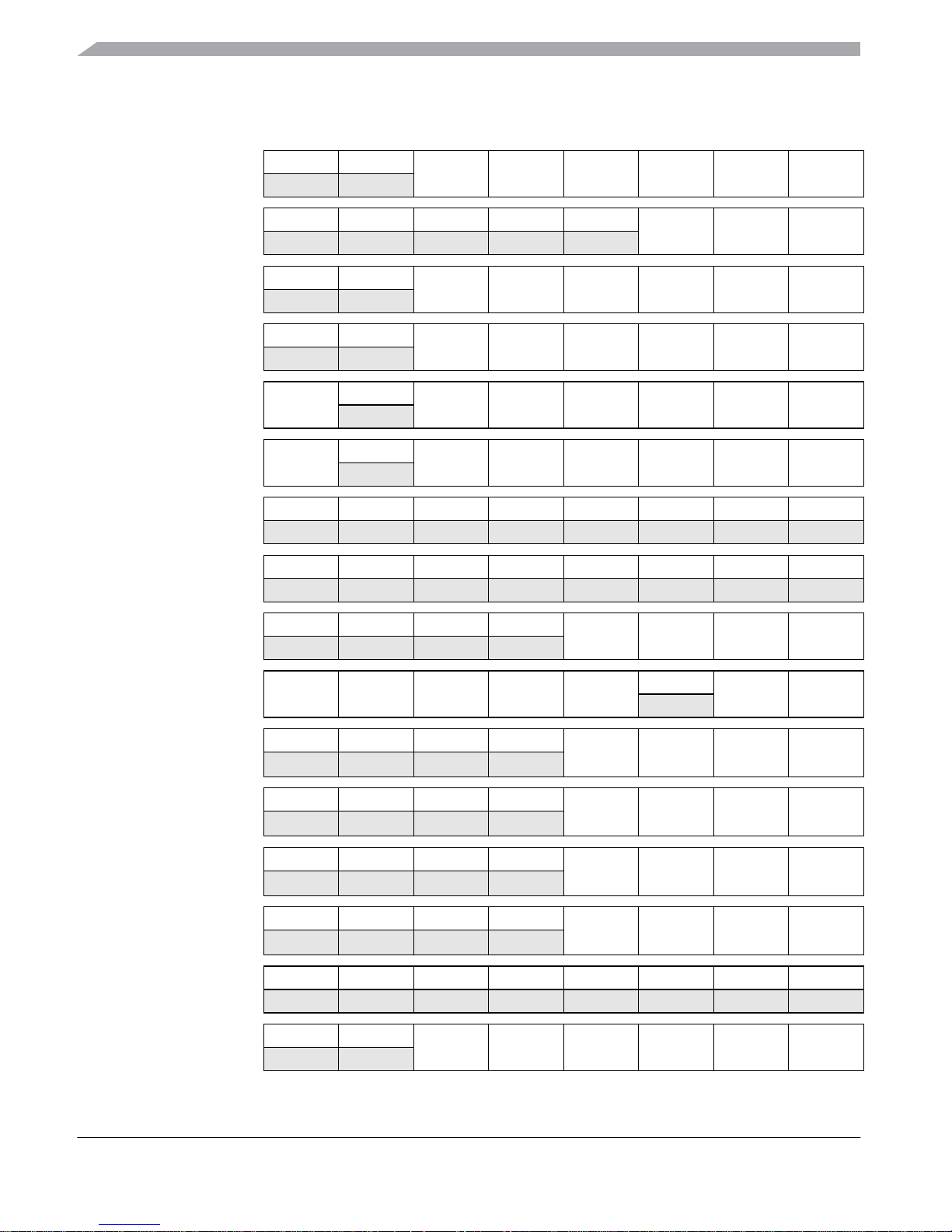
Port Integration Module (S12VRPIMV2)
MC9S12VR Family Reference Manual, Rev. 2.2
54 Freescale Semiconductor
Preliminary - Subject to Change Without Notice
0x025A DDRP
R0 0
DDRP5 DDRP4 DDRP3 DDRP2 DDRP1 DDRP0
W
0x025B RDRP
R00000
RDRP2 RDRP1 RDRP0
W
0x025C PERP
R0 0
PERP5 PERP4 PERP3 PERP2 PERP1 PERP0
W
0x025D PPSP
R0 0
PPSP5 PPSP4 PPSP3 PPSP2 PPSP1 PPSP0
W
0x025E PIEP
R
OCIE
0
PIEP5 PIEP4 PIEP3 PIEP2 PIEP1 PIEP0
W
0x025F PIFP
R
OCIF
0
PIFP5 PIFP4 PIFP3 PIFP2 PIFP1 PIFP0
W
0x0260–
0x0268
Reserved
R00000000
W
0x0269 PTIL
R0000PTIL3 PTIL2 PTIL1 PTIL0
W
0x026A DIENL
R0000
DIENL3 DIENL2 DIENL1 DIENL0
W
0x026B PTAL
R
PTTEL PTPSL PTABYPL PTADIRL PTAENL
0
PTAL1 PTAL0
W
0x026C PIRL
R0000
PIRL3 PIRL2 PIRL1 PIRL0
W
0x026D PPSL
R0000
PPSL3 PPSL2 PPSL1 PPSL0
W
0x026E PIEL
R0000
PIEL3 PIEL2 PIEL1 PIEL0
W
0x026F
PIFL
R0000
PIFL3 PIFL2 PIFL1 PIFL0
W
0x0270 Reserved
R00000000
W
0x0271 PT1AD
R0 0
PT1AD5 PT1AD4 PT1AD3 PT1AD2 PT1AD1 PT1AD0
W
Global
Address
Register
Name
Bit 7 654321Bit 0
Downloaded from Elcodis.com electronic components distributor
Page 55
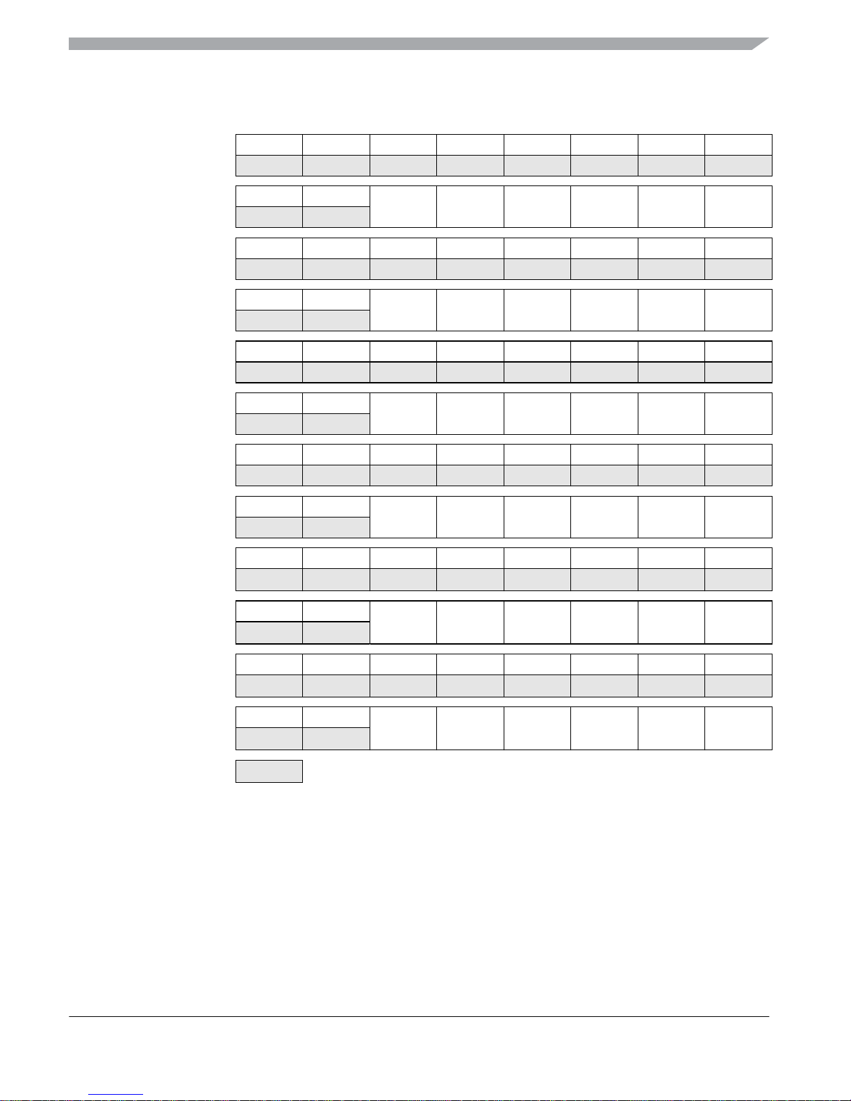
Port Integration Module (S12VRPIMV2)
MC9S12VR Family Reference Manual, Rev. 2.2
Freescale Semiconductor 55
Preliminary - Subject to Change Without Notice
2.3.2 Register Descriptions
The following table summarizes the effect of the various configuration bits, that is data direction (DDR),
output level (PORT/PT), pull enable (PER), pull select (PPS), interrupt enable (PIE) on the pin function,
pull device and interrupt activity.
The configuration bit PPS is used for two purposes:
1. Configure the sensitive interrupt edge (rising or falling), if interrupt is enabled.
0x0272 Reserved
R00000000
W
0x0273 PTI1AD
R0 0
PTI1AD5 PTI1AD4 PTI1AD3 PTI1AD2 PTI1AD1 PTI1AD0
W
0x0274 Reserved
R00000000
W
0x0275 DDR1AD
R0 0
DDR1AD5 DDR1AD4 DDR1AD3 DDR1AD2 DDR1AD1 DDR1AD0
W
0x0276–
0x0278
Reserved
R00000000
W
0x0279 PER1AD
R0 0
PER1AD5 PER1AD4 PER1AD3 PER1AD2 PER1AD1 PER1AD0
W
0x027A Reserved
R00000000
W
0x027B PPS1AD
R0 0
PPS1AD5 PPS1AD4 PPS1AD3 PPS1AD2 PPS1AD1 PPS1AD0
W
0x027C Reserved
R00000000
W
0x027D PIE1AD
R0 0
PIE1AD5 PIE1AD4 PIE1AD3 PIE1AD2 PIE1AD1 PIE1AD0
W
0x027E Reserved
R00000000
W
0x027F PIF1AD
R0 0
PIF1AD5 PIF1AD4 PIF1AD3 PIF1AD2 PIF1AD1 PIF1AD0
W
= Unimplemented
Global
Address
Register
Name
Bit 7 654321Bit 0
Downloaded from Elcodis.com electronic components distributor
Page 56
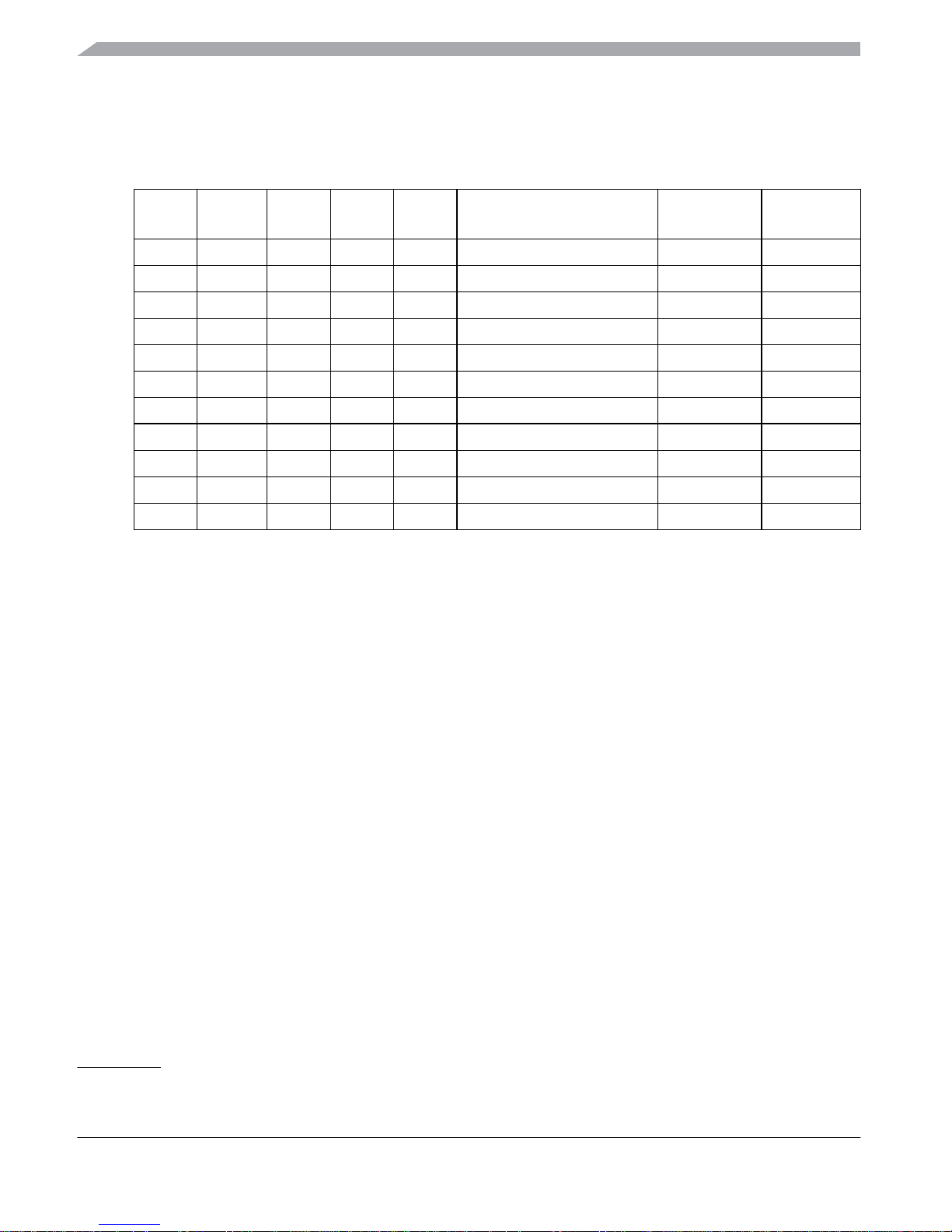
Port Integration Module (S12VRPIMV2)
MC9S12VR Family Reference Manual, Rev. 2.2
56 Freescale Semiconductor
Preliminary - Subject to Change Without Notice
2. Select either a pullup or pulldown device if PER is active.
Table 2-3. Pin Configuration Summary
1
NOTE
• All register bits in this module are completely synchronous to internal
clocks during a register read.
• Figure of port data registers also display the alternative functions if
applicable on the related pin as defined in Table 2-2. Names in
parentheses denote the availability of the function when using a specific
routing option.
• Figures of module routing registers also display the module instance or
module channel associated with the related routing bit.
DDR
PORT
PT
PER PPS
1
1
Always “0” on Port E
PIE
2
2
Applicable only on Port P and AD
Function Pull Device Interrupt
0 x 0 x 0 Input Disabled Disabled
0 x 1 0 0 Input Pullup Disabled
0 x 1 1 0 Input Pulldown Disabled
0 x 0 0 1 Input Disabled Falling edge
0 x 0 1 1 Input Disabled Rising edge
0 x 1 0 1 Input Pullup Falling edge
0 x 1 1 1 Input Pulldown Rising edge
1 0 x x 0 Output, drive to 0 Disabled Disabled
1 1 x x 0 Output, drive to 1 Disabled Disabled
1 0 x 0 1 Output, drive to 0 Disabled Falling edge
1 1 x 1 1 Output, drive to 1 Disabled Rising edge
1. Not applicable for Port L. Refer to register descriptions.
Downloaded from Elcodis.com electronic components distributor
Page 57
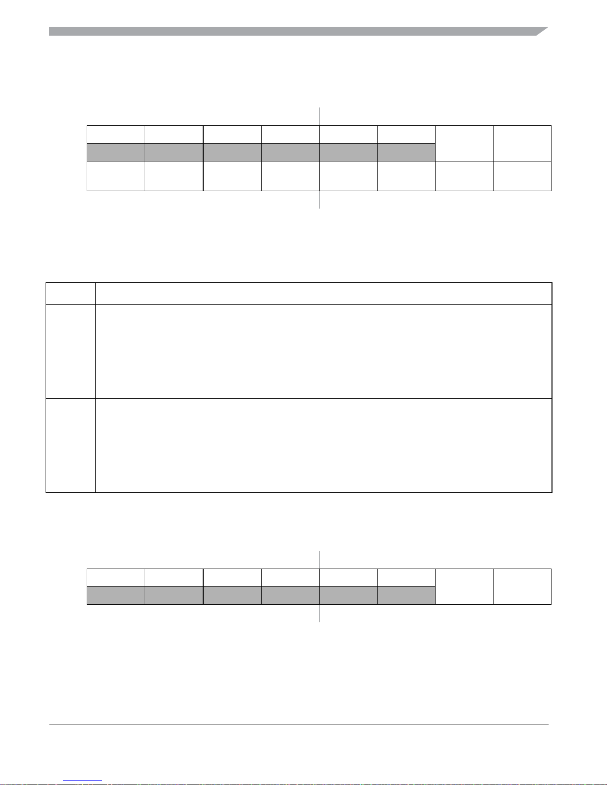
Port Integration Module (S12VRPIMV2)
MC9S12VR Family Reference Manual, Rev. 2.2
Freescale Semiconductor 57
Preliminary - Subject to Change Without Notice
2.3.3 Port E Data Register (PORTE)
2.3.4 Port E Data Direction Register (DDRE)
Address 0x0008 Access: User read/write
1
1
Read: Anytime. The data source is depending on the data direction value.
Write: Anytime
76543210
R000000
PE1 PE0
W
Altern.
Function
——————XTAL EXTAL
Reset 00000000
Figure 2-1. Port E Data Register (PORTE)
Table 2-4. PORTE Register Field Descriptions
Field Description
1
PE
PorT data register port E — General-purpose input/output data, CPMU OSC XTAL signal
If the CPMU OSC function is active this pin is used as XTAL signal and the pulldown device is
disabled. When not used with the alternative function, this pin can be used as general-purpose I/O.
In general-purpose output mode the register bit is driven to the pin.
If the associated data direction bit of this pin is set to 1, a read returns the value of the port register, otherwise the
synchronized pin input state is read.
• The CPMU OSC function takes precedence over the general purpose I/O function if enabled.
0
PE
PorT data register port E — General-purpose input/output data, CPMU OSC EXTAL signal
If the CPMU OSC function is active this pin is used as EXTAL signal and the pulldown device is
disabled. When not used with the alternative function, this pin can be used as general-purpose I/O.
In general-purpose output mode the register bit is driven to the pin.
If the associated data direction bit of this pin is set to 1, a read returns the value of the port register, otherwise the
synchronized pin input state is read.
• The CPMU OSC function takes precedence over the general purpose I/O function if enabled.
Address 0x0009 Access: User read/write
1
1
Read: Anytime
Write: Anytime
76543210
R000000
DDRE1 DDRE0
W
Reset 00000000
Figure 2-2. Port E Data Direction Register (DDRE)
Downloaded from Elcodis.com electronic components distributor
Page 58
Port Integration Module (S12VRPIMV2)
MC9S12VR Family Reference Manual, Rev. 2.2
58 Freescale Semiconductor
Preliminary - Subject to Change Without Notice
2.3.5 Port E, BKGD pin Pull Control Register (PUCR)
2.3.6 ECLK Control Register (ECLKCTL)
Table 2-5. DDRE Register Field Descriptions
Field Description
1-0
DDRE
Data Direction Register port E —
This bit determines whether the associated pin is an input or output.
1 Associated pin is configured as output
0 Associated pin is configured as input
Address 0x000C Access: User read/write
1
1
Read:Anytime
Write:Anytime, except BKPUE, which is writable in special mode only
76543210
R0
BKPUE
0
PDPEE
0000
W
Reset 01010000
Figure 2-3. Port E, BKGD pin Pull Control Register (PUCR)
Table 2-6. PUCR Register Field Descriptions
Field Description
6
BKPUE
BKGD pin Pullup Enable — Activate pullup device on pin
This bit configures whether a pullup device is activated, if the pin is used as input. If a pin is used as output this bit
has no effect.
1 Pullup device enabled
0 Pullup device disabled
4
PDPEE
Pull-Down Port E Enable — Activate pulldown devices on all port input pins
This bit configures whether a pulldown device is activated on all associated port input pins. If a pin is used as output
or used with the CPMU OSC function this bit has no effect. Out of reset the pulldown devices are enabled.
1 Pulldown devices enabled
0 Pulldown devices disabled
Address 0x001C Access: User read/write
1
76543210
R
NECLK
0000000
W
Reset 10000000
Figure 2-4. ECLK Control Register (ECLKCTL)
Downloaded from Elcodis.com electronic components distributor
Page 59
Port Integration Module (S12VRPIMV2)
MC9S12VR Family Reference Manual, Rev. 2.2
Freescale Semiconductor 59
Preliminary - Subject to Change Without Notice
2.3.7 PIM Miscellaneous Register (PIMMISC)
2.3.8 IRQ Control Register (IRQCR)
1
Read: Anytime
Write: Anytime
Table 2-7. ECLKCTL Register Field Descriptions
Field Description
7
NECLK
No ECLK — Disable ECLK output
This bit controls the availability of a free-running clock on the ECLK pin. This clock has a fixed rate equivalent to the
internal bus clock.
1 ECLK disabled
0 ECLK enabled
Address 0x001D Access: User read/write
1
1
Read: Anytime
Write: Anytime
76543210
R
OCPE
0000000
W
Reset 00000000
Figure 2-5. PIM Miscellaneous Register (PIMMISC)
Table 2-8. PIMMISC Register Field Descriptions
Field Description
7
OCPE
Over-Current Protection Enable— Activate over-current detector on PP2
Refer to Section 2.5.3, “Over-Current Protection on EVDD”
1 PP2 over-current detector enabled
0 PP2 over-current detector disabled
Address 0x001E Access: User read/write
1
76543210
R
IRQE IRQEN
000000
W
Reset 00000000
Figure 2-6. IRQ Control Register (IRQCR)
Downloaded from Elcodis.com electronic components distributor
Page 60
Port Integration Module (S12VRPIMV2)
MC9S12VR Family Reference Manual, Rev. 2.2
60 Freescale Semiconductor
Preliminary - Subject to Change Without Notice
2.3.9 Reserved Register
NOTE
These reserved registers are designed for factory test purposes only and are
not intended for general user access. Writing to these registers when in
special modes can alter the module’s functionality.
1
Read: Anytime
Write:
IRQE: Once in normal mode, anytime in special mode
IRQEN: Anytime
Table 2-9. IRQCR Register Field Descriptions
Field Description
7
IRQE
IRQ select Edge sensitive only —
1
IRQ pin configured to respond only to falling edges. Falling edges on the IRQ pin will be detected anytime IRQE=1
and will be cleared only upon a reset or the servicing of the
IRQ interrupt.
0
IRQ pin configured for low level recognition
6
IRQEN
IRQ ENable —
1
IRQ pin is connected to interrupt logic
0
IRQ pin is disconnected from interrupt logic
Address 0x001F Access: User read/write
1
1
Read: Anytime
Write: Only in special mode
76543210
R
Reserved Reserved Reserved Reserved Reserved Reserved Reserved Reserved
W
Reset xxxxxxxx
Figure 2-7. Reserved Register
Downloaded from Elcodis.com electronic components distributor
Page 61
Port Integration Module (S12VRPIMV2)
MC9S12VR Family Reference Manual, Rev. 2.2
Freescale Semiconductor 61
Preliminary - Subject to Change Without Notice
2.3.10 Port T Data Register (PTT)
Address 0x0240 Access: User read/write
1
1
Read: Anytime. The data source is depending on the data direction value.
Write: Anytime
76543210
R0000
PTT3 PTT2 PTT1 PTT0
W
Altern.
Function
————(SS) (SCK) PWM7
2
2
PWM function available on this pin only if not used with a routed HSDRV or LSDRV function. Refer to Section 2.3.15, “Module
Routing Register 0 (MODRR0)”
PWM6
2
————(LPTXD) (LPRXD) (TXD0) (RXD0)
——————(LPDR1) —
————IOC3
3
3
TIM output compare function available on this pin only if not used with routed HSDRV. Refer to Section 2.3.15, “Module Routing
Register 0 (MODRR0)”. TIM input capture function available on this pin only if not used with LPRXD. Refer to Section 2.3.23,
“Module Routing Register 2 (MODRR2)”.
IOC2
4
4
TIM output compare function available on this pin only if not used with routed HSDRV. Refer to Section 2.3.15, “Module Routing
Register 0 (MODRR0)”
IOC1
5
5
TIM output compare function available on this pin only if not used with routed LSDRV. Refer to Section 2.3.15, “Module Routing
Register 0 (MODRR0)”
IOC0
5
Reset 00000000
Figure 2-8. Port T Data Register (PTT)
Table 2-10. PTT Register Field Descriptions
Field Description
3-2
PTT
PorT data register port T — General-purpose input/output data, SPI
SS and SCK, TIM input/output, routed LINPHY
When not used with the alternative function, the associated pin can be used as general-purpose I/O. In
general-purpose output mode the register bit value is driven to the pin.
If the associated data direction bit is set to 1, a read returns the value of the port register bit, otherwise the
synchronized pin input state is read.
• The routed SPI takes precedence over the routed LINPHY function, TIM output function and the general-purpose
I/O function if enabled.
• The routed LINPHY function takes precedence over the TIM output function and the general-purpose I/O function
if the related channel is enabled.
• The TIM function takes precedence over the general-purpose I/O function.
Downloaded from Elcodis.com electronic components distributor
Page 62
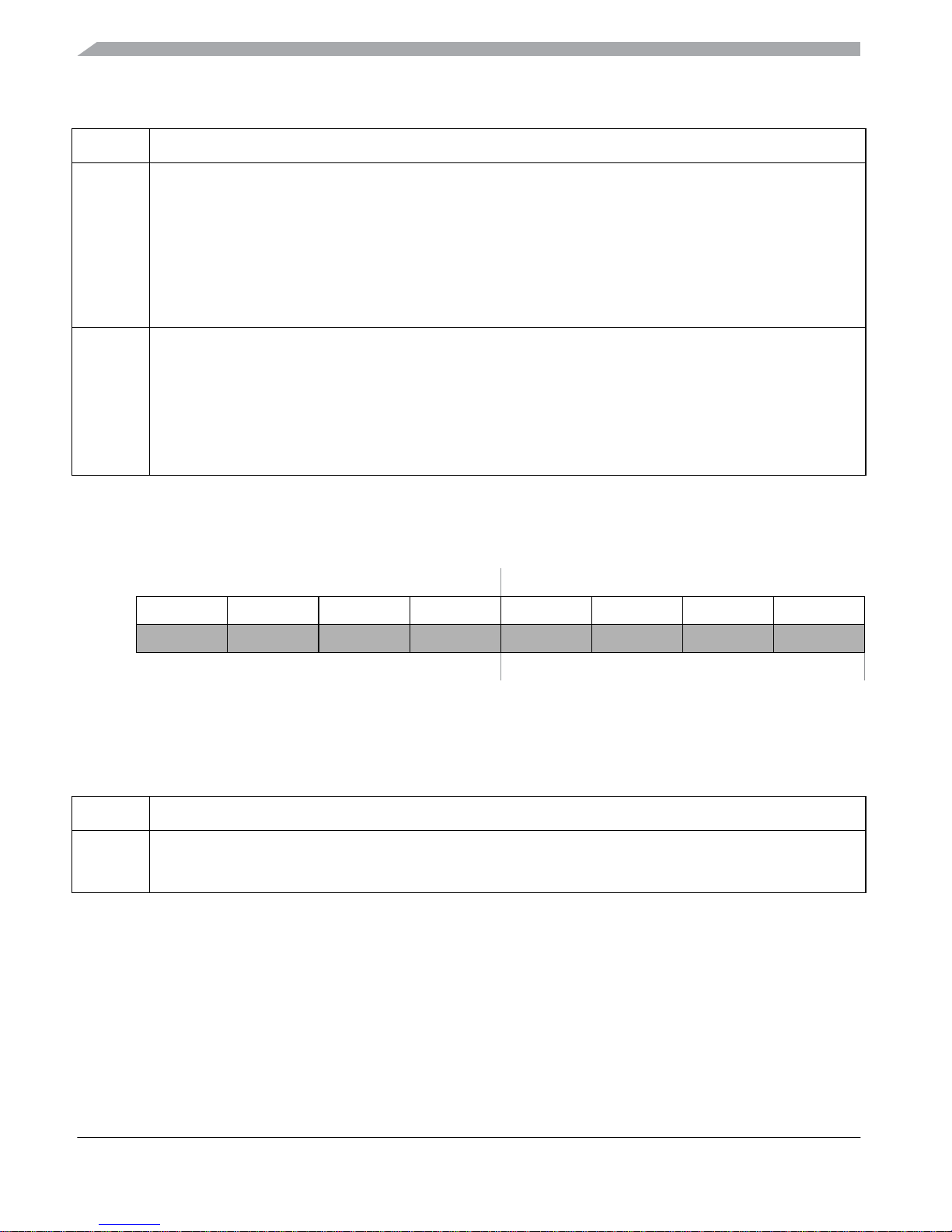
Port Integration Module (S12VRPIMV2)
MC9S12VR Family Reference Manual, Rev. 2.2
62 Freescale Semiconductor
Preliminary - Subject to Change Without Notice
2.3.11 Port T Input Register (PTIT)
1
PTT
PorT data register port T — General-purpose input/output data, TIM input/output, routed SCI0, LPDR[LPDR1]
When not used with the alternative function, the associated pin can be used as general-purpose I/O. In
general-purpose output mode the register bit value is driven to the pin.
If the associated data direction bit is set to 1, a read returns the value of the port register bit, otherwise the
synchronized pin input state is read.
• The routed SCI0 or LPDR[LPDR1] takes precedence over the TIM output function and the general-purpose I/O
function if enabled.
• The TIM function takes precedence over the general-purpose I/O function if enabled.
0
PTT
PorT data register port T — General-purpose input/output data, TIM input/output, routed SCI0
When not used with the alternative function, the associated pin can be used as general-purpose I/O. In
general-purpose output mode the register bit value is driven to the pin.
If the associated data direction bit is set to 1, a read returns the value of the port register bit, otherwise the
synchronized pin input state is read.
• The routed SCI0 takes precedence over the TIM output function and the general-purpose I/O function if enabled.
• The TIM function takes precedence over the general-purpose I/O function if enabled.
Address 0x0241 Access: User read only
1
1
Read: Anytime
Write:Never
76543210
R0000PTIT3 PTIT2 PTIT1 PTIT0
W
Reset 00000000
Figure 2-9. Port T Input Register (PTIT)
Table 2-11. PTIT Register Field Descriptions
Field Description
3-0
PTIT
PorT Input data register port T —
A read always returns the synchronized input state of the associated pin. It can be used to detect overload or short
circuit conditions on output pins.
Table 2-10. PTT Register Field Descriptions (continued)
Field Description
Downloaded from Elcodis.com electronic components distributor
Page 63

Port Integration Module (S12VRPIMV2)
MC9S12VR Family Reference Manual, Rev. 2.2
Freescale Semiconductor 63
Preliminary - Subject to Change Without Notice
2.3.12 Port T Data Direction Register (DDRT)
Address 0x0242 Access: User read/write
1
1
Read: Anytime
Write: Anytime
76543210
R0000
DDRT3 DDRT2 DDRT1 DDRT0
W
Reset 00000000
Figure 2-10. Port T Data Direction Register (DDRT)
Table 2-12. DDRT Register Field Descriptions
Field Description
3
DDRT
Data Direction Register port T —
This bit determines whether the pin is an input or output
Depending on the configuration of the enabled SPI the I/O state will be forced to be input or output. The enabled
routed LINPHY forces the I/O state to be an input (LPTXD). Else the TIM forces the I/O state to be an output for a
TIM port associated with an enabled TIM output compare. In these cases the data direction bit will not change.
1 Associated pin is configured as output
0 Associated pin is configured as input
2
DDRT
Data Direction Register port T —
This bit determines whether the pin is an input or output.
Depending on the configuration of the enabled SPI the I/O state will be forced to be input or output. The enabled
routed LINPHY forces the I/O state to be an output (LPRXD). Else the TIM forces the I/O state to be an output for a
TIM port associated with an enabled TIM output compare. In these cases the data direction bit will not change.
1 Associated pin is configured as output
0 Associated pin is configured as input
1-0
DDRT
Data Direction Register port T —
This bit determines whether the pin is an input or output.
Depending on the configuration of the enabled routed SCI0 the I/O state will be forced to be input or output. The
enabled routed LINPHY forces the I/O state to be an output (LPDR[LPDR1]). Else the TIM forces the I/O state to be
an output for a TIM port associated with an enabled TIM output compare. In these cases the data direction bit will
not change.
1 Associated pin is configured as output
0 Associated pin is configured as input
Downloaded from Elcodis.com electronic components distributor
Page 64
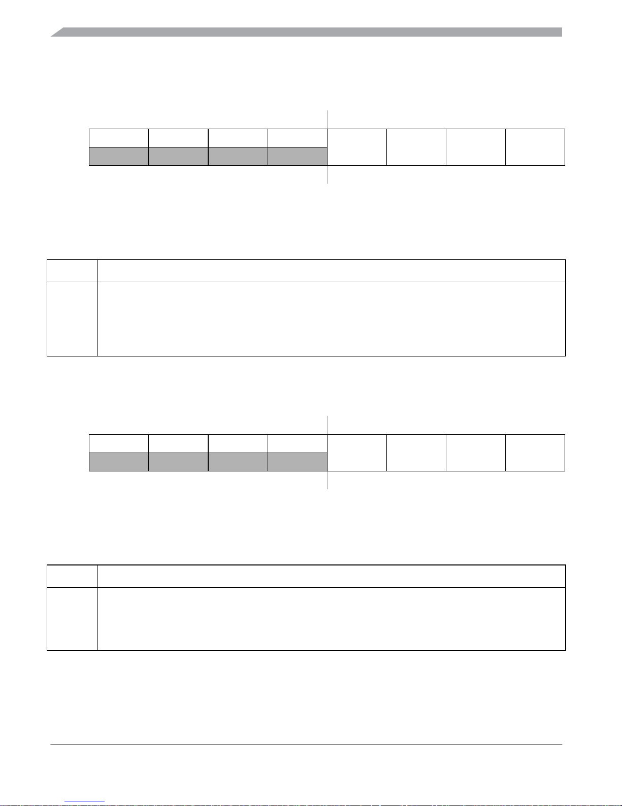
Port Integration Module (S12VRPIMV2)
MC9S12VR Family Reference Manual, Rev. 2.2
64 Freescale Semiconductor
Preliminary - Subject to Change Without Notice
2.3.13 Port T Pull Device Enable Register (PERT)
2.3.14 Port T Polarity Select Register (PPST)
Address 0x0244 Access: User read/write
1
1
Read: Anytime
Write: Anytime
76543210
R0000
PERT3 PERT2 PERT1 PERT0
W
Reset 00000000
Figure 2-11. Port T Pull Device Enable Register (PERT)
Table 2-13. PERT Register Field Descriptions
Field Description
3-0
PERT
Pull device Enable Register port T — Enable pull device on input pin
This bit controls whether a pull device on the associated port input pin is active. If a pin is used as output this bit has
no effect. The polarity is selected by the related polarity select register bit.
1 Pull device enabled
0 Pull device disabled
Address 0x0245 Access: User read/write
1
1
Read: Anytime
Write: Anytime
76543210
R0000
PPST3 PPST2 PPST1 PPST0
W
Reset 00000000
Figure 2-12. Port T Polarity Select Register (PPST)
Table 2-14. PPST Register Field Descriptions
Field Description
3-0
PPST
Pull device Polarity Select register port T — Configure pull device polarity on input pin
This bit selects a pullup or a pulldown device if enabled on the associated port input pin.
1 A pulldown device is selected
0 A pullup device is selected
Downloaded from Elcodis.com electronic components distributor
Page 65
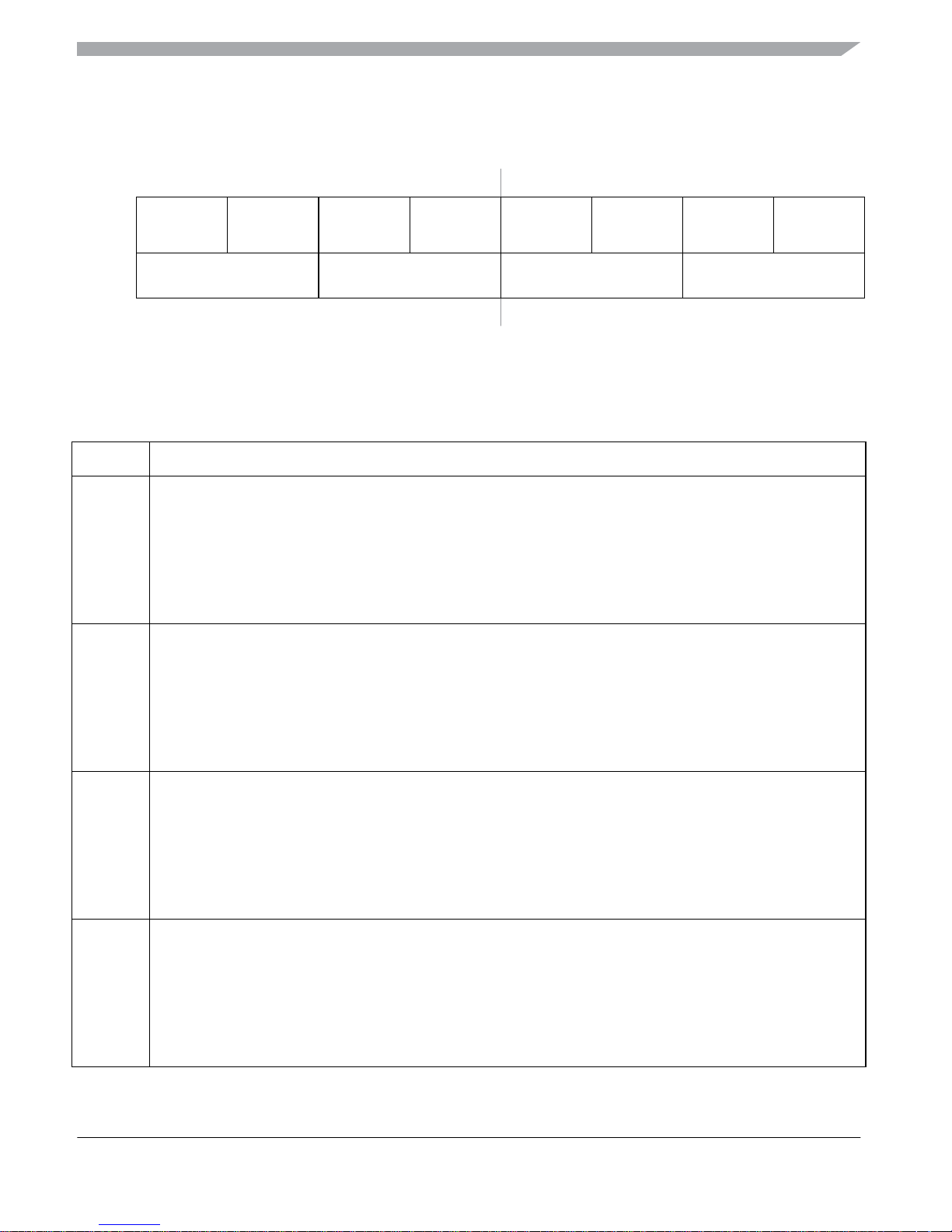
Port Integration Module (S12VRPIMV2)
MC9S12VR Family Reference Manual, Rev. 2.2
Freescale Semiconductor 65
Preliminary - Subject to Change Without Notice
2.3.15 Module Routing Register 0 (MODRR0)
Address 0x0246 Access: User read/write
1
1
Read: Anytime
Write: Once in normal, anytime in special mode
76543210
R
MODRR07 MODRR06 MODRR05 MODRR04 MODRR03 MODRR02 MODRR01 MODRR00
W
Routing
Option
HS1 HS0 LS1 LS0
Reset 00000000
Figure 2-13. Module Routing Register 0 (MODRR0)
Table 2-15. Module Routing Register 0 Field Descriptions
Field Description
7-6
MODRR0
MODule Routing Register 0 — HS1
This register controls the routing of PWM and TIM channels to pin HS1 of HSDRV module. By default the pin is
controlled by the related HSDRV port register bit.
11 PWM channel 1 routed to HS1 if enabled
10 PWM channel 4 routed to HS1 if enabled
01 TIM output compare channel 3 routed to HS1 if enabled
00 HS1 controlled by register bit HSDR[HSDR1]. Refer to HSDRV section.
5-4
MODRR0
MODule Routing Register 0 — HS0
This register controls the routing of PWM and TIM channels to pin HS0 of HSDRV module. By default the pin is
controlled by the related HSDRV port register bit.
11 PWM channel 3 routed to HS0 if enabled
10 PWM channel 3 routed to HS0 if enabled
01 TIM output compare channel 2 routed to HS0 if enabled
00 HS0 controlled by register bit HSDR[HSDR0]. Refer to HSDRV section.
3-2
MODRR0
MODule Routing Register 0 — LS1
This register controls the routing of PWM and TIM channels to pin LS1 of LSDRV module. By default the pin is
controlled by the related LSDRV port register bit.
11 PWM channel 7 routed to LS1 if enabled
10 PWM channel 7 routed to LS1 if enabled
01 TIM output compare channel 1 routed to LS1 if enabled
00 LS1 controlled by register bit LSDR[LSDR1]. Refer to LSDRV section.
1-0
MODRR0
MODule Routing Register 0 — LS0
This register controls the routing of PWM and TIM channels to pin LS0 of LSDRV module. By default the pin is
controlled by the related LSDRV port register bit.
11 PWM channel 5 routed to LS0 if enabled
10 PWM channel 6 routed to LS0 if enabled
01 TIM output compare channel 0 routed to LS0 if enabled
00 LS0 controlled by register bit LSDR[LSDR0]. Refer to LSDRV section.
Downloaded from Elcodis.com electronic components distributor
Page 66
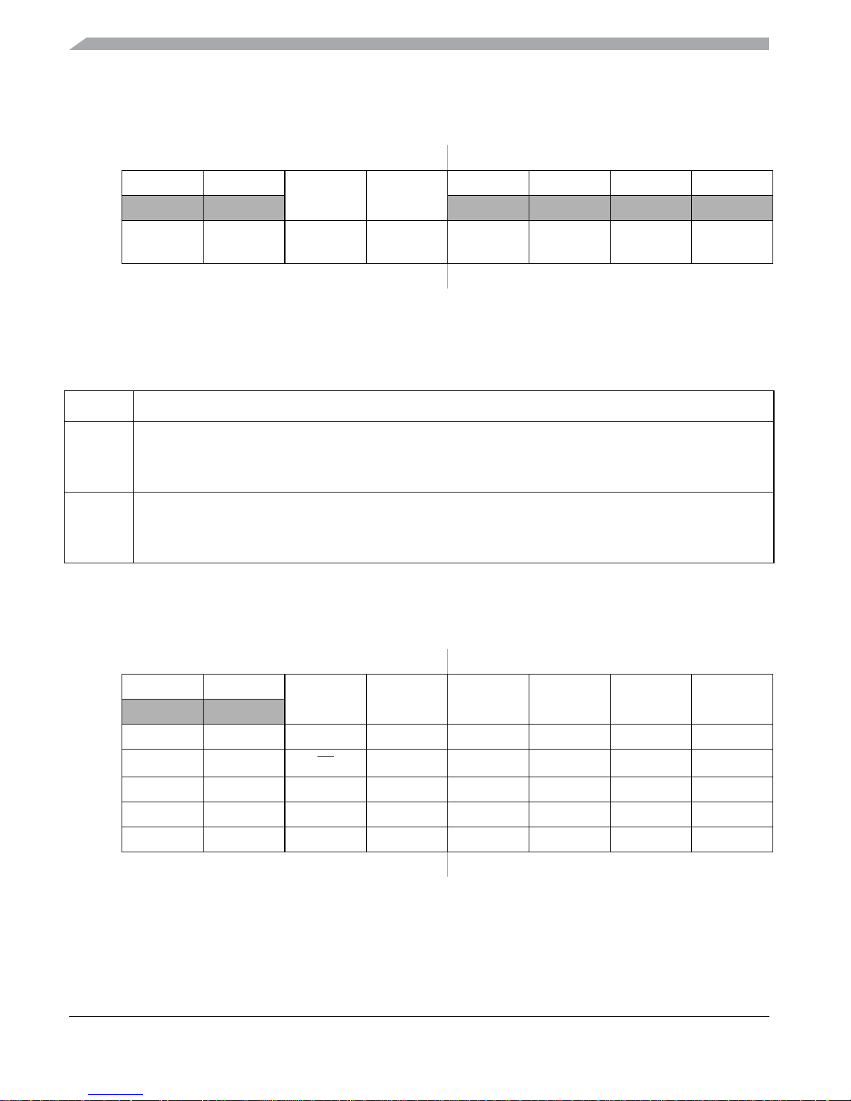
Port Integration Module (S12VRPIMV2)
MC9S12VR Family Reference Manual, Rev. 2.2
66 Freescale Semiconductor
Preliminary - Subject to Change Without Notice
2.3.16 Module Routing Register 1 (MODRR1)
2.3.17 Port S Data Register (PTS)
Address 0x0247 Access: User read/write
1
1
Read: Anytime
Write: Once in normal, anytime in special mode
76543210
R0 0
MODRR15 MODRR14
0000
W
Routing
Option
——
PWM5
ETRIG1
PWM4
ETRIG0
————
Reset 00000000
Figure 2-14. Module Routing Register 1 (MODRR1)
Table 2-16. Module Routing Register 1 Field Descriptions
Field Description
5
MODRR1
MODule Routing Register 1 — PWM5, ETRIG1
1 PWM channel 5 on PS3; ETRIG1 on PS3
0 PWM channel 5 on PP5; ETRIG1 on PP5
4
MODRR1
MODule Routing Register 1 — PWM4, ETRIG0
1 PWM channel 4 on PS2; ETRIG0 on PS2
0 PWM channel 4 on PP4; ETRIG0 on PP4
Address 0x0248 Access: User read/write
1
1
Read: Anytime. The data source is depending on the data direction value.
Write: Anytime
76543210
R0 0
PTS5 PTS4 PTS3 PTS2 PTS1 PTS0
W
Altern.
Function
————ECLK — — —
——
SS SCK MOSI MISO — —
————(TXD1) (RXD1) TXD1 RXD1
————(PWM5
2
)
2
PWM function available on this pin only if not used with a routed HSDRV or LSDRV function. Refer to Section 2.3.15, “Module
Routing Register 0 (MODRR0)”
(PWM4
2
) (LPDR1) —
————(ETRIG1) (ETRIG0) (TXD0) (RXD0)
Reset 00000000
Figure 2-15. Port S Data Register (PTS)
Downloaded from Elcodis.com electronic components distributor
Page 67

Port Integration Module (S12VRPIMV2)
MC9S12VR Family Reference Manual, Rev. 2.2
Freescale Semiconductor 67
Preliminary - Subject to Change Without Notice
Table 2-17. PTS Register Field Descriptions
Field Description
5
PTS
PorT data register port S — General-purpose input/output data, SPI
SS
When not used with the alternative function, the associated pin can be used as general-purpose I/O. In
general-purpose output mode the register bit value is driven to the pin.
If the associated data direction bit is set to 1, a read returns the value of the port register bit, otherwise the
synchronized pin input state is read.
• The SPI function takes precedence over the general-purpose I/O function if enabled.
4
PTS
PorT data register port S — General-purpose input/output data, SPI SCK
When not used with the alternative function, the associated pin can be used as general-purpose I/O. In
general-purpose output mode the register bit value is driven to the pin.
If the associated data direction bit is set to 1, a read returns the value of the port register bit, otherwise the
synchronized pin input state is read.
• The SPI function takes precedence over the general-purpose I/O function if enabled.
3
PTS
PorT data register port S — General-purpose input/output data, ECLK, SPI MOSI, routed SCI1, routed PWM,
routed ETRIG
When not used with the alternative function, the associated pin can be used as general-purpose I/O. In
general-purpose output mode the register bit value is driven to the pin.
If the associated data direction bit is set to 1, a read returns the value of the port register bit, otherwise the
synchronized pin input state is read.
• The ECLK output function takes precedence over the SPI, routed SCI1 and PWM and the general purpose I/O
function if enabled.
• The SPI function takes precedence over the routed SCI1, routed PWM and the general purpose I/O function if
enabled.
• The routed SCI1 function takes precedence over the PWM and general-purpose I/O function if enabled.
• The routed PWM function takes precedence over the general-purpose I/O function if enabled.
2
PTS
PorT data register port S — General-purpose input/output data, SPI MISO, routed SCI1, routed PWM, routed
ETRIG
When not used with the alternative function, the associated pin can be used as general-purpose I/O. In
general-purpose output mode the register bit value is driven to the pin.
If the associated data direction bit is set to 1, a read returns the value of the port register bit, otherwise the
synchronized pin input state is read.
• The SPI function takes precedence over the routed SCI1, routed PWM and the general purpose I/O function if
enabled.
• The routed SCI1 function takes precedence over the routed PWM and the general-purpose I/O function if enabled.
• The routed PWM function takes precedence over the general-purpose I/O function if enabled.
Downloaded from Elcodis.com electronic components distributor
Page 68
Port Integration Module (S12VRPIMV2)
MC9S12VR Family Reference Manual, Rev. 2.2
68 Freescale Semiconductor
Preliminary - Subject to Change Without Notice
2.3.18 Port S Input Register (PTIS)
1
PTS
PorT data register port S — General-purpose input/output data, SCI1, routed SCI0 or LPDR[LPDR1]
When not used with the alternative function, the associated pin can be used as general-purpose I/O. In
general-purpose output mode the register bit value is driven to the pin.
If the associated data direction bit is set to 1, a read returns the value of the port register bit, otherwise the
synchronized pin input state is read.
• The SCI1 function takes precedence over the routed SCI0 or LPDR[LPDR1] function and the general-purpose I/O
function if enabled.
• The routed SCI0 or LPDR[LPDR1] function takes precedence over the general-purpose I/O function if enabled.
0
PTS
PorT data register port S — General-purpose input/output data, SCI1, routed SCI0
When not used with the alternative function, the associated pin can be used as general-purpose I/O. In
general-purpose output mode the register bit value is driven to the pin.
If the associated data direction bit is set to 1, a read returns the value of the port register bit, otherwise the
synchronized pin input state is read.
• The SCI1 function takes precedence over the routed SCI0 function and the general-purpose I/O function if
enabled.
• The routed SCI0 function takes precedence over the general-purpose I/O function if enabled.
Address 0x0249 Access: User read only
1
1
Read: Anytime
Write:Never
76543210
R 0 0 PTIS5 PTIS4 PTIS3 PTIS2 PTIS1 PTIS0
W
Reset 00000000
Figure 2-16. Port S Input Register (PTIS)
Table 2-18. PTIS Register Field Descriptions
Field Description
5-0
PTIS
PorT Input data register port S —
A read always returns the synchronized input state of the associated pin. It can be used to detect overload or short
circuit conditions on output pins.
Table 2-17. PTS Register Field Descriptions (continued)
Field Description
Downloaded from Elcodis.com electronic components distributor
Page 69

Port Integration Module (S12VRPIMV2)
MC9S12VR Family Reference Manual, Rev. 2.2
Freescale Semiconductor 69
Preliminary - Subject to Change Without Notice
2.3.19 Port S Data Direction Register (DDRS)
Address 0x024A Access: User read/write
1
1
Read: Anytime
Write: Anytime
76543210
R0 0
DDRS5 DDRS4 DDRS3 DDRS2 DDRS1 DDRS0
W
Reset 00000000
Figure 2-17. Port S Data Direction Register (DDRS)
Table 2-19. DDRS Register Field Descriptions
Field Description
5
DDRS
Data Direction Register port S —
This bit determines whether the associated pin is an input or output. Depending on the configuration of the enabled
SPI the I/O state will be forced to be input or output. In this case the data direction bit will not change.
1 Associated pin is configured as output
0 Associated pin is configured as input
4
DDRS
Data Direction Register port S —
This bit determines whether the associated pin is an input or output. Depending on the configuration of the enabled
SPI the I/O state will be forced to be input or output. In this case the data direction bit will not change.
1 Associated pin is configured as output
0 Associated pin is configured as input
3
DDRS
Data Direction Register port S —
This bit determines whether the associated pin is an input or output. The ECLK output function, routed SCI1 and
routed PWM function forces the I/O state to output if enabled. Depending on the configuration of the enabled SPI
the I/O state will be forced to be input or output. In these cases the data direction bit will not change. The routed
ETRIG function has no effect on the I/O state.
1 Associated pin is configured as output
0 Associated pin is configured as input
2
DDRS
Data Direction Register port S —
This bit determines whether the associated pin is an input or output. Depending on the configuration of the enabled
SPI the I/O state will be forced to be input or output. The routed SCI1 function forces the I/O state to input if enabled.
The routed PWM function forces the I/O state to output if enabled. In these cases the data direction bit will not
change. The routed ETRIG function has no effect on the I/O state.
1 Associated pin is configured as output
0 Associated pin is configured as input
Downloaded from Elcodis.com electronic components distributor
Page 70
Port Integration Module (S12VRPIMV2)
MC9S12VR Family Reference Manual, Rev. 2.2
70 Freescale Semiconductor
Preliminary - Subject to Change Without Notice
2.3.20 Port S Pull Device Enable Register (PERS)
1
DDRS
Data Direction Register port S —
This bit determines whether the associated pin is an input or output.
Depending on the configuration of the enabled SCI the I/O state will be forced to be input or output. The enabled
routed LINPHY forces the I/O state to be an output (LPDR[LPDR1]). In these cases the data direction bit will not
change.
1 Associated pin is configured as output
0 Associated pin is configured as input
0
DDRS
Data Direction Register port S —
This bit determines whether the associated pin is an input or output.
Depending on the configuration of the enabled SCI the I/O state will be forced to be input or output. In this case the
data direction bit will not change.
1 Associated pin is configured as output
0 Associated pin is configured as input
Address 0x024C Access: User read/write
1
1
Read: Anytime
Write: Anytime
76543210
R0 0
PERS5 PERS4 PERS3 PERS2 PERS1 PERS0
W
Reset 00111111
Figure 2-18. Port S Pull Device Enable Register (PERS)
Table 2-20. PERS Register Field Descriptions
Field Description
5-0
PERS
Pull device Enable Register port S — Enable pull device on input pin or wired-or output pin
This bit controls whether a pull device on the associated port input pin is active. If a pin is used as output this bit has
only effect if used in wired-or mode. The polarity is selected by the related polarity select register bit.
1 Pull device enabled
0 Pull device disabled
Table 2-19. DDRS Register Field Descriptions (continued)
Field Description
Downloaded from Elcodis.com electronic components distributor
Page 71
Port Integration Module (S12VRPIMV2)
MC9S12VR Family Reference Manual, Rev. 2.2
Freescale Semiconductor 71
Preliminary - Subject to Change Without Notice
2.3.21 Port S Polarity Select Register (PPSS)
2.3.22 Port S Wired-Or Mode Register (WOMS)
Address 0x024D Access: User read/write
1
1
Read: Anytime
Write: Anytime
76543210
R0 0
PPSS5 PPSS4 PPSS3 PPSS2 PPSS1 PPSS0
W
Reset 00000000
Figure 2-19. Port S Polarity Select Register (PPSS)
Table 2-21. PPSS Register Field Descriptions
Field Description
5-0
PPSS
Pull device Polarity Select register port S — Configure pull device polarity on input pin
This bit selects a pullup or a pulldown device if enabled on the associated port input pin.
1 A pulldown device is selected
0 A pullup device is selected
Address 0x024E Access: User read/write
1
1
Read: Anytime
Write: Anytime
76543210
R0 0
WOMS5 WOMS4 WOMS3 WOMS2 WOMS1 WOMS0
W
Reset 00000000
Figure 2-20. Port S Wired-Or Mode Register (WOMS)
Table 2-22. WOMS Register Field Descriptions
Field Description
5-0
WOMS
Wired-Or Mode register port S — Enable open-drain functionality on output pin
This bit configures an output pin as wired-or (open-drain) or push-pull. In wired-or mode a logic “0” is driven
active-low while a logic “1” remains undriven. This allows a multipoint connection of several serial modules. The bit
has no influence on pins used as input.
1 Output buffer operates as open-drain output
0 Output buffer operates as push-pull output
Downloaded from Elcodis.com electronic components distributor
Page 72
Port Integration Module (S12VRPIMV2)
MC9S12VR Family Reference Manual, Rev. 2.2
72 Freescale Semiconductor
Preliminary - Subject to Change Without Notice
2.3.23 Module Routing Register 2 (MODRR2)
Address 0x024F Access: User read/write
1
1
Read: Anytime
Write: Once in normal, anytime in special mode
76543210
R
MODRR27
0
MODRR25 MODRR24 MODRR23 MODRR22 MODRR21 MODRR20
W
Routing
Option
LPRXD to
TIM
—
SPI
SS and SCK
SCI1 SCI0-to-LINPHY interface
Reset 00000000
Figure 2-21. Module Routing Register 2 (MODRR2)
Table 2-23. Module Routing Register 2 Field Descriptions
Field Description
7
MODRR2
MODule Routing Register 2 — TIM routing
1 TIM input capture channel 3 is connected to LPRXD
0 TIM input capture channel 3 is connected to PT3
5
MODRR2
MODule Routing Register 2 — SPI
SS and SCK routing
1
SS on PT3; SCK on PT2
0
SS on PS5; SCK on PS4
4
MODRR2
MODule Routing Register 2 — SCI1 routing
1 TXD1 on PS3; RXD1 on PS2
0 TXD1 on PS1; RXD1 on PS0
3-0
MODRR2
MODule Routing Register 2 — SCI0-to-LINPHY routing
Selection of SCI0-to-LINPHY interface routing options to support probing and conformance testing. Refer to
Figure 2-22 for an illustration and Table 2-24 for preferred settings. SCI0 must be enabled for TXD0 routing to take
effect on pins. LINPHY must be enabled for LPRXD and LPDR[LPDR1] routings to take effect on pins.
Downloaded from Elcodis.com electronic components distributor
Page 73
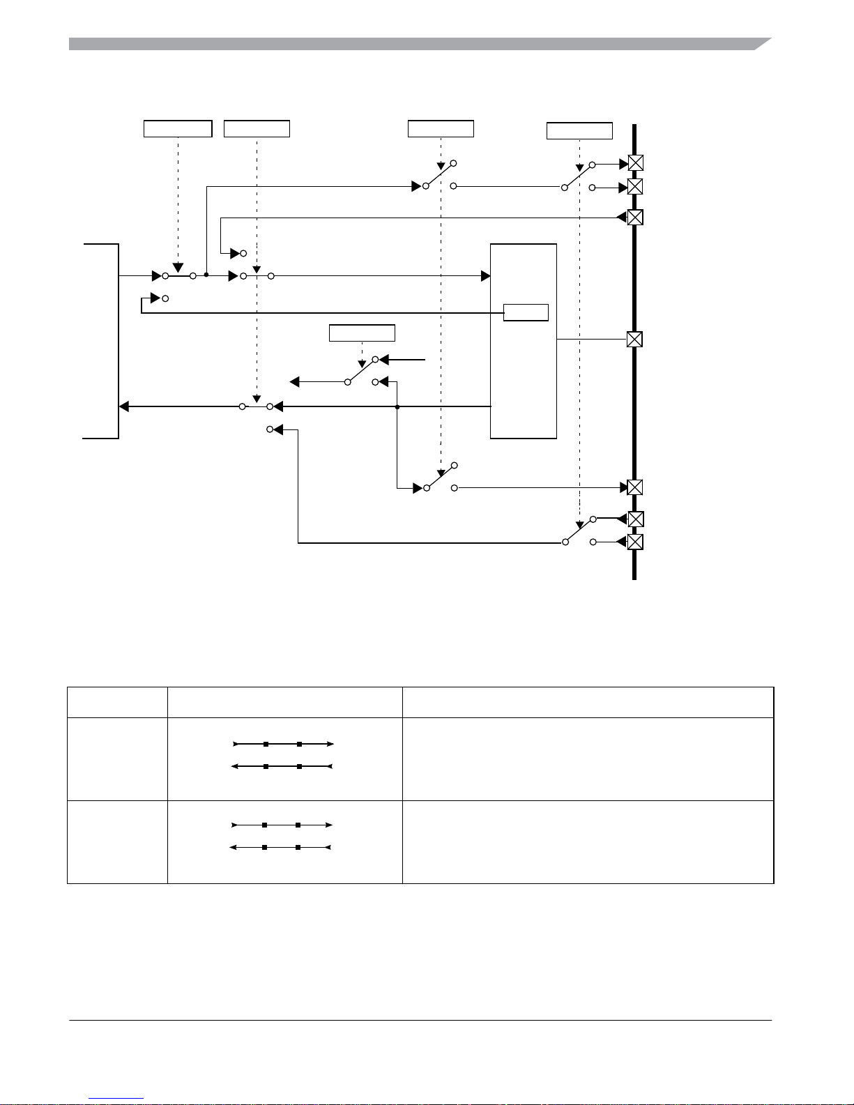
Port Integration Module (S12VRPIMV2)
MC9S12VR Family Reference Manual, Rev. 2.2
Freescale Semiconductor 73
Preliminary - Subject to Change Without Notice
Figure 2-22. SCI0-to-LINPHY Routing Options Illustration
Table 2-24. Preferred Interface Configurations
MODRR2[3:0] Signal Routing Description
0000 Default setting:
SCI0 connects to LINPHY, interface internal only
0001 Direct control setting:
LPDR[LPDR1] register bit controls LPTXD, interface internal only
MODRR27
IOC3
PT2 / LPRXD
PT3 / LPTXD
PT1 / TXD0 / LPDR1
PT0 / RXD0
0
1
0
1
0
1
1
0
1
0
1
0
TIM input
capture
channel 3
MODRR22MODRR21MODRR20
SCI0
LINPHY
TXD0
RXD0
LPTXD
LPRXD
1
0
1
0
MODRR23
PS0 / RXD0
PS1 / TXD0 / LPDR1
LPDR1
LIN
Downloaded from Elcodis.com electronic components distributor
Page 74
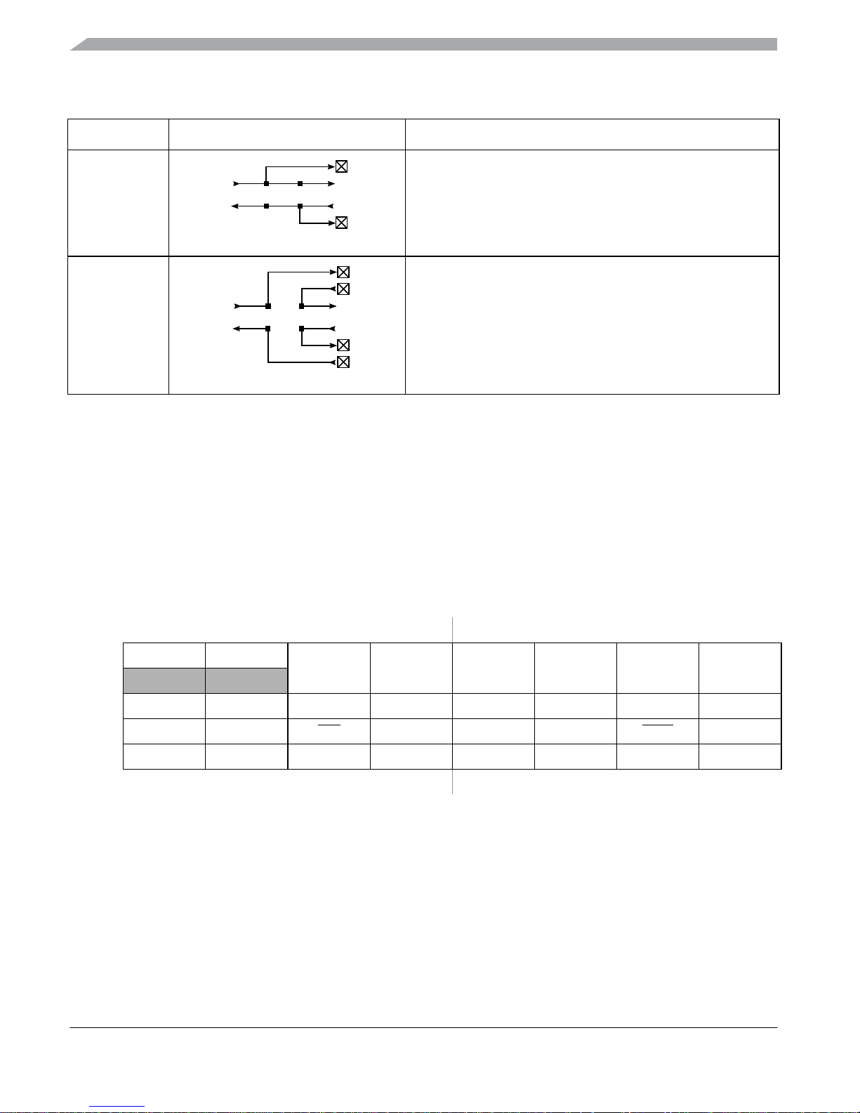
Port Integration Module (S12VRPIMV2)
MC9S12VR Family Reference Manual, Rev. 2.2
74 Freescale Semiconductor
Preliminary - Subject to Change Without Notice
NOTE
For standalone usage of SCI0 on external pins set MODRR2[3:0]=0b1110
and disable the LINPHY (LPCR[LPE]=0). This releases PT2 and PT3 to
other associated functions and maintains TXD0 and RXD0 signals on PT1
and PT0, respectively, if no other function with higher priority takes
precedence.
2.3.24 Port P Data Register (PTP)
1100 Probe setting:
SCI0 connects to LINPHY, interface accessible on 2 external pins
1110 Conformance test setting:
Interface opened and all 4 signals routed externally
Address 0x0258 Access: User read/write
1
1
Read: Anytime. The data source is depending on the data direction value.
Write: Anytime
76543210
R0 0
PTP5 PTP4 PTP3 PTP2 PTP1 PTP0
W
Altern.
Function
— — PWM5
23
2
PWM function available on this pin only if not used with a routed HSDRV or LSDRV function. Refer to Section 2.3.15, “Module
Routing Register 0 (MODRR0)”
3
PWM function available on this pin only if not routed to port S. Refer to Section 2.3.16, “Module Routing Register 1 (MODRR1)”
PWM4
23
PWM3
2
PWM2 PWM1
2
PWM0
——IRQ — — EVDD XIRQ —
— — ETRIG1 ETRIG0 — — — —
Reset 00000000
Figure 2-23. Port P Data Register (PTP)
MODRR2[3:0] Signal Routing Description
Downloaded from Elcodis.com electronic components distributor
Page 75

Port Integration Module (S12VRPIMV2)
MC9S12VR Family Reference Manual, Rev. 2.2
Freescale Semiconductor 75
Preliminary - Subject to Change Without Notice
Table 2-25. PTP Register Field Descriptions
Field Description
5
PTP
PorT data register port P — General-purpose input/output data, PWM output, ETRIG input, pin interrupt
input/output,
IRQ input
The
IRQ signal is mapped to this pin when used with the IRQ interrupt function. If enabled
(IRQCR[IRQEN]=1) the I/O state of the pin is forced to be an input.
When not used with the alternative function, the associated pin can be used as general-purpose I/O. In
general-purpose output mode the register bit value is driven to the pin.
If the associated data direction bit is set to 1, a read returns the value of the port register bit, otherwise the
synchronized pin input state is read.
• The IRQ function takes precedence over the PWM and the general-purpose I/O function if enabled.
• The PWM function takes precedence over the general-purpose I/O function if the related channel is enabled.
• Pin interrupts can be generated if enabled in input or output mode.
• The ETRIG function has no effect on the I/O state.
4
PTP
PorT data register port P — General-purpose input/output data, PWM output, ETRIG input, pin interrupt
input/output
The associated pin can be used as general-purpose I/O. In general-purpose output mode the register bit value is
driven to the pin.
If the associated data direction bit is set to 1, a read returns the value of the port register bit, otherwise the
synchronized pin input state is read.
• The PWM function takes precedence over the general-purpose I/O function if the related channel is enabled.
• Pin interrupts can be generated if enabled in input or output mode.
• The ETRIG function has no effect on the I/O state.
3
PTP
PorT data register port P — General-purpose input/output data, PWM output, pin interrupt input/output
The associated pin can be used as general-purpose I/O. In general-purpose output mode the register bit value is
driven to the pin.
If the associated data direction bit is set to 1, a read returns the value of the port register bit, otherwise the
synchronized pin input state is read.
• The PWM function takes precedence over the general-purpose I/O function if the related channel is enabled.
• Pin interrupts can be generated if enabled in input or output mode.
2
PTP
PorT data register port P — General-purpose input/output data, PWM output, switchable high-current capable
external supply with over-current protection (EVDD)
The associated pin can be used as general-purpose I/O or as a supply for external devices such as Hall sensors
(see Section 2.5.3, “Over-Current Protection on EVDD”. In output mode the register bit value is driven to the pin.
If the associated data direction bit is set to 1, a read returns the value of the port register bit, otherwise the
synchronized pin input state is read.
• The PWM function takes precedence over the general-purpose I/O function if the related channel is enabled.
• Pin interrupts can be generated if enabled in input or output mode.
• An over-current interrupt can be generated if enabled. Refer to Section 2.4.4.3, “Over-Current Interrupt”
Downloaded from Elcodis.com electronic components distributor
Page 76
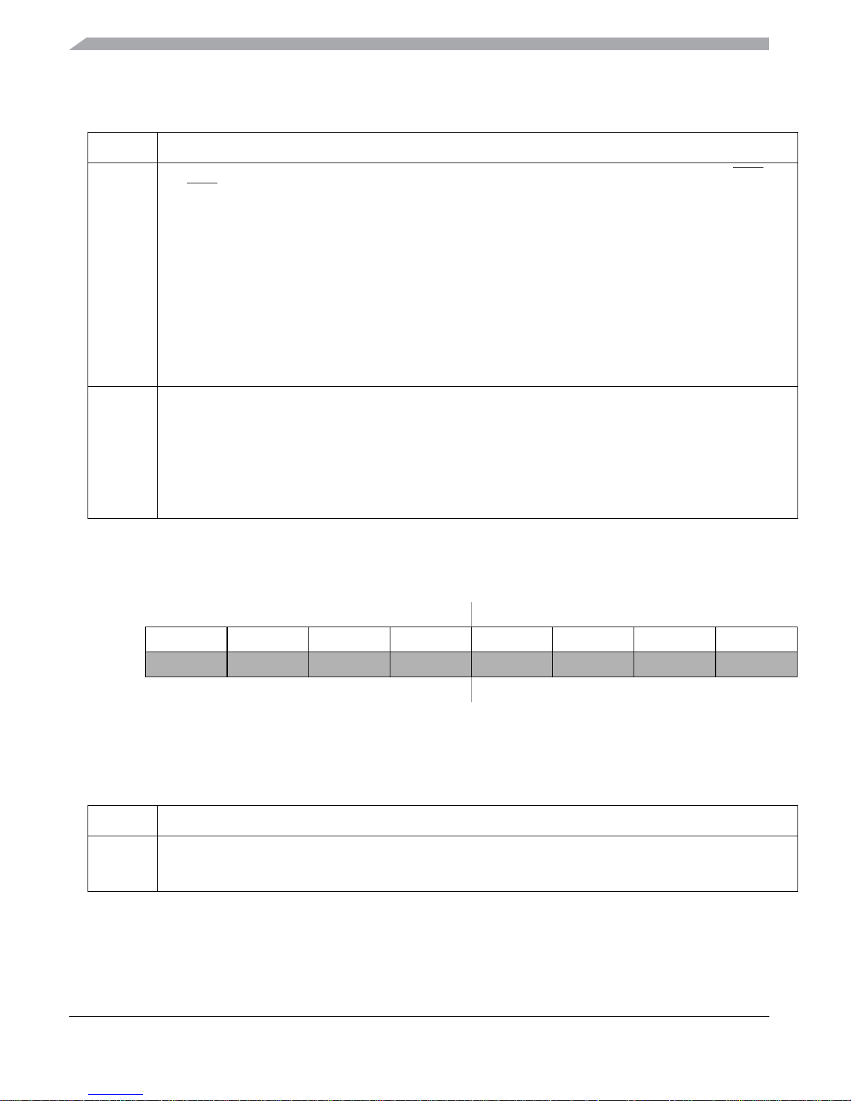
Port Integration Module (S12VRPIMV2)
MC9S12VR Family Reference Manual, Rev. 2.2
76 Freescale Semiconductor
Preliminary - Subject to Change Without Notice
2.3.25 Port P Input Register (PTIP)
1
PTP
PorT data register port P — General-purpose input/output data, PWM output, pin interrupt input/output, XIRQ input
The
XIRQ signal is mapped to this pin when used with the XIRQ interrupt function. The
interrupt is enabled by clearing the X mask bit in the CPU Condition Code register. The I/O state of the
pin is forced to input level upon the first clearing of the X bit and held in this state even if the bit is set
again. A stop or wait recovery with the X bit set (refer to CPU12/CPU12X Reference Manual) is not
available.
When not used with the alternative function, the associated pin can be used as general-purpose I/O. In
general-purpose output mode the register bit value is driven to the pin.
If the associated data direction bit is set to 1, a read returns the value of the port register bit, otherwise the
synchronized pin input state is read.
• The XIRQ function takes precedence over the PWM and the general-purpose I/O function if enabled.
• The PWM function takes precedence over the general-purpose I/O function if the related channel is enabled.
• Pin interrupts can be generated if enabled in input or output mode.
0
PTP
PorT data register port P — General-purpose input/output data, PWM output, pin interrupt input/output
When not used with the alternative function, the associated pin can be used as general-purpose I/O. In
general-purpose output mode the register bit value is driven to the pin.
If the associated data direction bit is set to 1, a read returns the value of the port register bit, otherwise the
synchronized pin input state is read.
• The PWM function takes precedence over the general-purpose I/O function if the related channel is enabled.
• Pin interrupts can be generated if enabled in input or output mode.
Address 0x0259 Access: User read only
1
1
Read: Anytime
Write:Never
76543210
R 0 0 PTIP5 PTIP4 PTIP3 PTIP2 PTIP1 PTIP0
W
Reset 0 0000000
Figure 2-24. Port P Input Register (PTIP)
Table 2-26. PTIP Register Field Descriptions
Field Description
5-0
PTIP
PorT Input data register port P —
A read always returns the synchronized input state of the associated pin. It can be used to detect overload or short
circuit conditions on output pins.
Table 2-25. PTP Register Field Descriptions (continued)
Field Description
Downloaded from Elcodis.com electronic components distributor
Page 77

Port Integration Module (S12VRPIMV2)
MC9S12VR Family Reference Manual, Rev. 2.2
Freescale Semiconductor 77
Preliminary - Subject to Change Without Notice
2.3.26 Port P Data Direction Register (DDRP)
Address 0x025A Access: User read/write
1
1
Read: Anytime
Write: Anytime
76543210
R0 0
DDRP5 DDRP4 DDRP3 DDRP2 DDRP1 DDRP0
W
Reset 00000000
Figure 2-25. Port P Data Direction Register (DDRP)
Table 2-27. DDRP Register Field Descriptions
Field Description
5
DDRP
Data Direction Register port P —
This bit determines whether the associated pin is an input or output.
The enabled IRQ function forces the I/O state to be an input if enabled. In this case the data direction bit will not
change.
1 Associated pin is configured as output
0 Associated pin is configured as input
4-2
DDRP
Data Direction Register port P —
This bit determines whether the associated pin is an input or output.
1 Associated pin is configured as output
0 Associated pin is configured as input
1
DDRP
Data Direction Register port P —
This bit determines whether the associated pin is an input or output.
The I/O state of the pin is forced to input level upon the first clearing of the X bit and held in this state even if the bit
is set again. The PWM forces the I/O state to be an output for an enabled channel. In this case the data direction bit
will not change.
1 Associated pin is configured as output
0 Associated pin is configured as input
0
DDRP
Data Direction Register port P —
This bit determines whether the associated pin is an input or output.
The PWM forces the I/O state to be an output for an enabled channel. In this case the data direction bit will not
change.
1 Associated pin is configured as output
0 Associated pin is configured as input
Downloaded from Elcodis.com electronic components distributor
Page 78
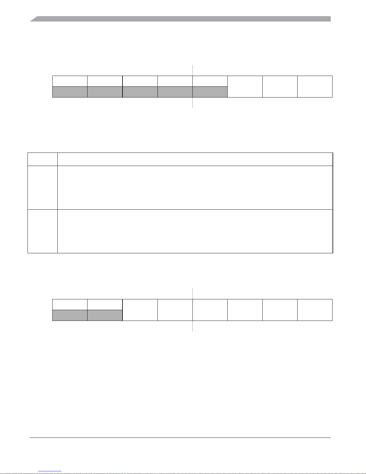
Port Integration Module (S12VRPIMV2)
MC9S12VR Family Reference Manual, Rev. 2.2
78 Freescale Semiconductor
Preliminary - Subject to Change Without Notice
2.3.27 Port P Reduced Drive Register (RDRP)
2.3.28 Port P Pull Device Enable Register (PERP)
Address 0x025B Access: User read/write
1
1
Read: Anytime
Write: Anytime
76543210
R00000
RDRP2 RDRP1 RDRP0
W
Reset 00000000
Figure 2-26. Port P Reduced Drive Register (RDRP)
Table 2-28. RDRP Register Field Descriptions
Field Description
2
RDRP
Reduced Drive Register port P — Select reduced drive for output pin
This bit configures the drive strength of the associated output pin as either full or reduced. If a pin is used as input
this bit has no effect. The reduced drive function is independent of which function is being used on a particular pin.
1 Reduced drive selected (approx. 1/10 of the full drive strength)
0 Full drive strength enabled
1-0
RDRP
Reduced Drive Register port P — Select reduced drive for output pin
This bit configures the drive strength of the associated output pin as either full or reduced. If a pin is used as input
this bit has no effect. The reduced drive function is independent of which function is being used on a particular pin.
1 Reduced drive selected (approx. 1/5 of the full drive strength)
0 Full drive strength enabled
Address 0x025C Access: User read/write
1
1
Read: Anytime
Write: Anytime
76543210
R0 0
PERP5 PERP4 PERP3 PERP2 PERP1 PERP0
W
Reset 00000000
Figure 2-27. Port P Pull Device Enable Register (PERP)
Downloaded from Elcodis.com electronic components distributor
Page 79
Port Integration Module (S12VRPIMV2)
MC9S12VR Family Reference Manual, Rev. 2.2
Freescale Semiconductor 79
Preliminary - Subject to Change Without Notice
2.3.29 Port P Polarity Select Register (PPSP)
2.3.30 Port P Interrupt Enable Register (PIEP)
Read: Anytime.
Table 2-29. PERP Register Field Descriptions
Field Description
5-0
PERP
Pull device Enable Register port P — Enable pull device on input pin
This bit controls whether a pull device on the associated port input pin is active. If a pin is used as output this bit has
no effect. The polarity is selected by the related polarity select register bit.
1 Pull device enabled
0 Pull device disabled
Address 0x025D Access: User read/write
1
1
Read: Anytime
Write: Anytime
76543210
R0 0
PPSP5 PPSP4 PPSP3 PPSP2 PPSP1 PPSP0
W
Reset 00000000
Figure 2-28. Port P Polarity Select Register (PPSP)
Table 2-30. PPSP Register Field Descriptions
Field Description
5-0
PPSP
Pull device Polarity Select register port P — Configure pull device polarity and pin interrupt edge polarity on input
pin
This bit selects a pullup or a pulldown device if enabled on the associated port input pin.
This bit also selects the polarity of the active pin interrupt edge.
1 A pulldown device is selected; rising edge selected
0 A pullup device is selected; falling edge selected
Address 0x025E Access: User read/write
1
1
Read: Anytime
Write: Anytime
76543210
R
OCIE
0
PIEP5 PIEP4 PIEP3 PIEP2 PIEP1 PIEP0
W
Reset 00000000
Figure 2-29. Port P Interrupt Enable Register (PIEP)
Downloaded from Elcodis.com electronic components distributor
Page 80
Port Integration Module (S12VRPIMV2)
MC9S12VR Family Reference Manual, Rev. 2.2
80 Freescale Semiconductor
Preliminary - Subject to Change Without Notice
2.3.31 Port P Interrupt Flag Register (PIFP)
Table 2-31. PIEP Register Field Descriptions
Field Description
7
OCIE
Over-Current Interrupt Enable register port P —
This bit enables or disables the over-current interrupt on PP2.
1 PP2 over-current interrupt enabled
0 PP2 over-current interrupt disabled (interrupt flag masked)
5-0
PIEP
Pin Interrupt Enable register port P —
This bit enables or disables the edge sensitive pin interrupt on the associated pin. An interrupt can be generated if
the pin is operating in input or output mode when in use with the general-purpose or related peripheral function.
1 Interrupt is enabled
0 Interrupt is disabled (interrupt flag masked)
Address 0x025F Access: User read/write
1
1
Read: Anytime
Write: Anytime, write 1 to clear
76543210
R
OCIF
0
PIFP5 PIFP4 PIFP3 PIFP2 PIFP1 PIFP0
W
Reset 00000000
Figure 2-30. Port P Interrupt Flag Register (PIFP)
Table 2-32. PIFP Register Field Descriptions
Field Description
7
OCIF
Over-Current Interrupt Flag register port P —
This flag asserts if an over-current condition is detected on PP2 (Section 2.4.4.3, “Over-Current Interrupt”).
1 PP2 Over-current event occurred
0 No PP2 over-current event occurred
5-0
PIFP
Pin Interrupt Flag register port P —
This flag asserts after a valid active edge was detected on the related pin (Section 2.4.4, “Interrupts”). This can be
a rising or a falling edge based on the state of the polarity select register. An interrupt will occur if the associated
interrupt enable bit is set.
1 Active edge on the associated bit has occurred
0 No active edge occurred
Downloaded from Elcodis.com electronic components distributor
Page 81
Port Integration Module (S12VRPIMV2)
MC9S12VR Family Reference Manual, Rev. 2.2
Freescale Semiconductor 81
Preliminary - Subject to Change Without Notice
2.3.32 Port L Input Register (PTIL)
2.3.33 Port L Digital Input Enable Register (DIENL)
Address 0x0269 Access: User read only
1
1
Read: Anytime
Write: No Write
76543210
R0000PTIL3 PTIL2 PTIL1 PTIL0
W
Reset 00000000
Figure 2-31. Port L Input Register (PTIL)
Table 2-33. PTIL - Register Field Descriptions
Field Description
3-0
PTIL
PorT Input data register port L —
A read returns the synchronized input state if the associated pin is used in digital mode, that is the related
DIENL bit is set to 1 and the pin is not used in analog mode (PTAL[PTAENL]=1). See Section 2.3.34, “Port L
Analog Access Register (PTAL)”. A one is read in any other case
1
.
1
Refer to PTTEL bit description in Section 2.3.34, “Port L Analog Access Register (PTAL) for an override condition.
Address 0x26A Access: User read/write
1
1
Read: Anytime
Write: Anytime
76543210
R0000
DIENL3 DIENL2 DIENL1 DIENL0
W
Reset 00000000
Figure 2-32. Port L Digital Input Enable Register (DIENL)
Table 2-34. DIENL Register Field Descriptions
Field Description
3-0
DIENL
Digital Input ENable port L — Input buffer control
This bit controls the HVI digital input function. If set to 1 the input buffers are enabled and the pin can be used with
the digital function. If the analog input function is enabled (PTAL[PTAENL]=1) the input buffer of the selected HVI pin
is forced off
1
in run mode and is released to be active in stop mode only if DIENL=1.
1 Associated pin digital input is enabled if not used as analog input in run mode
1
0 Associated pin digital input is disabled
1
1
Refer to PTTEL bit description in Section 2.3.34, “Port L Analog Access Register (PTAL) for an override condition.
Downloaded from Elcodis.com electronic components distributor
Page 82

Port Integration Module (S12VRPIMV2)
MC9S12VR Family Reference Manual, Rev. 2.2
82 Freescale Semiconductor
Preliminary - Subject to Change Without Notice
2.3.34 Port L Analog Access Register (PTAL)
Address 0x026B Access: User read/write
1
1
Read: Anytime
Write: Anytime
76543210
R
PTTEL PTPSL PTABYPL PTADIRL PTAENL
0
PTAL1 PTAL0
W
Reset 00000000
Figure 2-33. Port L Analog Access Register (PTAL)
Table 2-35. PTAL Register Field Descriptions
Field Description
7
PTTEL
PorT Test Enable port L —
This bit forces the input buffer of the selected HVI pin (PTAL[1:0]) to be active while using the analog function to
support open input detection in run mode. Refer to Section 2.5.4, “Open Input Detection on HVI Pins”). In stop mode
this bit has no effect.
Note: In direct input connection (PTAL[PTADIRL]=1) the digital input buffer is not enabled.
1 Input buffer enabled when used with analog function and not in direct mode (PTAL[PTADIRL]=0)
0 Input buffer disabled when used with analog function
6
PTPSL
PorT Pull Select port L —
This bit selects a pull device on the selected HVI pin (PTAL[1:0]) in analog mode for open input detection. By default
a pulldown device is active as part of the input voltage divider. If set to 1 and PTTEL=1 and not in stop mode a pullup
to a level close to V
DDX
takes effect and overrides the weak pulldown device. Refer to Section 2.5.4, “Open Input
Detection on HVI Pins”).
1 Pullup enabled
0 Pulldown enabled
5
PTABYPL
PorT ADC connection BYPass port L —
This bit bypasses and powers down the impedance converter stage in the signal path from the analog input pin to
the ADC channel input. This bit takes effect only if using direct input connection to the ADC channel (PTADIRL=1).
1 Bypass impedance converter in ADC channel signal path
0 Use impedance converter in ADC channel signal path
4
PTADIRL
PorT ADC DIRect connection port L —
This bit connects the selected analog input signal (PTAL[1:0]) directly to the ADC channel bypassing the voltage
divider. This bit takes effect only in analog mode (PTAENL=1).
1 Input pin directly connected to ADC channel
0 Input voltage divider active on analog input to ADC channel
Downloaded from Elcodis.com electronic components distributor
Page 83
Port Integration Module (S12VRPIMV2)
MC9S12VR Family Reference Manual, Rev. 2.2
Freescale Semiconductor 83
Preliminary - Subject to Change Without Notice
NOTE
When enabling the resistor paths to ground by setting PTAL[PTAENL]=1
or by changing PTAL[PTAL1:PTAL0], a settling time of t
UNC_HVI
+ two
bus cycles must be considered to let internal nodes be loaded with correct
values.
3
PTAENL
PorT ADC connection ENable port L —
This bit enables the analog signal link of an HVI pin selected by PTAL[1:0] to an ADC channel. If set to 1 the analog
input function takes precedence over the digital input in run mode by forcing off the input buffers if not overridden by
PTTEL=1.
1 Selected pin by PTAL[1:0] is connected to ADC channel
0 No Port L pin is connected to ADC
1-0
PTAL
PorT ADC connection selector port L —
These selector bits choose the HVI pin connecting to an ADC channel if enabled (PTAENL=1). Refer to Table 2-36
for details.
Table 2-36. HVI pin connected to ADC channel
PTAL[PTAL1] PTAL[PTAL0]
HVI pin connected
to ADC
1
1
Refer to device overview section for channel assignment
0 0 HVI0
0 1 HVI1
1 0 HVI2
1 1 HVI3
Table 2-35. PTAL Register Field Descriptions (continued)
Field Description
Downloaded from Elcodis.com electronic components distributor
Page 84
Port Integration Module (S12VRPIMV2)
MC9S12VR Family Reference Manual, Rev. 2.2
84 Freescale Semiconductor
Preliminary - Subject to Change Without Notice
2.3.35 Port L Input Divider Ratio Selection Register (PIRL)
2.3.36 Port L Polarity Select Register (PPSL)
Address 0x026C Access: User read/write
1
1
Read: Anytime
Write: Anytime
76543210
R0000
PIRL3 PIRL2 PIRL1 PIRL0
W
Reset 00000000
Figure 2-34. Port L Input Divider Ratio Selection Register (PIRL)
Table 2-37. PIRL Register Field Descriptions
Field Description
3-0
PIRL
Port L Input Divider Ratio Select —
This bit selects one of two voltage divider ratios for the associated high-voltage input pin in analog mode.
1 Ratio
L_HVI
selected
0 Ratio
H_HVI
selected
Address 0x026D Access: User read/write
1
1
Read: Anytime
Write: Anytime
76543210
R0000
PPSL3 PPSL2 PPSL1 PPSL0
W
Reset 00000000
Figure 2-35. Port L Polarity Select Register (PPSL)
Table 2-38. PPSL Register Field Descriptions
Field Description
3-0
PPSL
Pin interrupt Polarity Select register port L —
This bit selects the polarity of the active pin interrupt edge.
1 Rising edge selected
0 Falling edge selected
Downloaded from Elcodis.com electronic components distributor
Page 85
Port Integration Module (S12VRPIMV2)
MC9S12VR Family Reference Manual, Rev. 2.2
Freescale Semiconductor 85
Preliminary - Subject to Change Without Notice
2.3.37 Port L Interrupt Enable Register (PIEL)
2.3.38 Port L Interrupt Flag Register (PIFL)
2.3.39 Port AD Data Register (PT1AD)
Address 0x026E Access: User read/write
1
1
Read: Anytime
Write: Anytime
76543210
R0000
PIEL3 PIEL2 PIEL1 PIEL0
W
Reset 00000000
Figure 2-36. Port L Interrupt Enable Register (PIEL)
Table 2-39. PIEL Register Field Descriptions
Field Description
3-0
PIEL
Pin Interrupt Enable register port L —
This bit enables or disables the edge sensitive pin interrupt on the associated pin. For wakeup from stop mode
this bit must be set.
1 Interrupt is enabled
0 Interrupt is disabled (interrupt flag masked)
Address 0x026F Access: User read/write
1
1
Read: Anytime
Write: Anytime, write 1 to clear
76543210
R0000
PIFL3 PIFL2 PIFL1 PIFL0
W
Reset 00000000
Figure 2-37. Port L Interrupt Flag Register (PIFL)
Table 2-40. PIFL Register Field Descriptions
Field Description
3-0
PIFL
Pin Interrupt Flag register port L —
This flag asserts after a valid active edge was detected on the related pin (Section 2.4.4, “Interrupts”). This
can be a rising or a falling edge based on the state of the polarity select register. An interrupt will occur if the
associated interrupt enable bit is set.
1 Active edge on the associated bit has occurred
0 No active edge occurred
Downloaded from Elcodis.com electronic components distributor
Page 86
Port Integration Module (S12VRPIMV2)
MC9S12VR Family Reference Manual, Rev. 2.2
86 Freescale Semiconductor
Preliminary - Subject to Change Without Notice
2.3.40 Port AD Input Register (PTI1AD)
Address 0x0271 Access: User read/write
1
1
Read: Anytime. The data source is depending on the data direction value.
Write: Anytime
76543210
R0 0
PT1AD5 PT1AD4 PT1AD3 PT1AD2 PT1AD1 PT1AD0
W
Altern.
Function
— — AN5 AN4 AN3 AN2 AN1 AN0
Reset 00000000
Figure 2-38. Port AD Data Register (PT1AD)
Table 2-41. PT1AD Register Field Descriptions
Field Description
5-0
PT1AD
PorT data register 1 port AD — General-purpose input/output data, ADC AN analog input
When not used with the alternative function, the associated pin can be used as general-purpose I/O. In
general-purpose output mode the register bit value is driven to the pin.
If the associated data direction bit set to 1, a read returns the value of the port register bit. If the data direction bit is
set to 0 and the ADC Digital Input Enable Register (ATDDIEN) is set to 1 the synchronized pin input state is read.
Address 0x0273 Access: User read only
1
1
Read: Anytime
Write:Never
76543210
R 0 0 PTI1AD5 PTI1AD4 PTI1AD3 PTI1AD2 PTI1AD1 PTI1AD0
W
Reset 00000000
u = Unaffected by reset
Figure 2-39. Port P Input Register (PTI1AD)
Table 2-42. PTI1AD Register Field Descriptions
Field Description
5-0
PTI1AD
PorT Input data register 1 port AD —
A read always returns the synchronized input state of the associated pin if the ADC Digital Input Enable Register
(ATDDIEN) is set to 1. Else a logic 1 is read. It can be used to detect overload or short circuit conditions on output
pins.
Downloaded from Elcodis.com electronic components distributor
Page 87
Port Integration Module (S12VRPIMV2)
MC9S12VR Family Reference Manual, Rev. 2.2
Freescale Semiconductor 87
Preliminary - Subject to Change Without Notice
2.3.41 Port AD Data Direction Register (DDR1AD)
Address 0x0275 Access: User read/write
1
1
Read: Anytime
Write: Anytime
76543210
R0 0
DDR1AD5 DDR1AD4 DDR1AD3 DDR1AD2 DDR1AD1 DDR1AD0
W
Reset 00000000
Figure 2-40. Port AD Data Direction Register (DDR1AD)
Table 2-43. DDR1AD Register Field Descriptions
Field Description
5-0
DDR1AD
Data Direction Register 1 port AD —
This bit determines whether the associated pin is an input or output.
To use the digital input function the ADC Digital Input Enable Register (ATDDIEN) has to be set to logic level “1”.
1 Associated pin is configured as output
0 Associated pin is configured as input
Downloaded from Elcodis.com electronic components distributor
Page 88
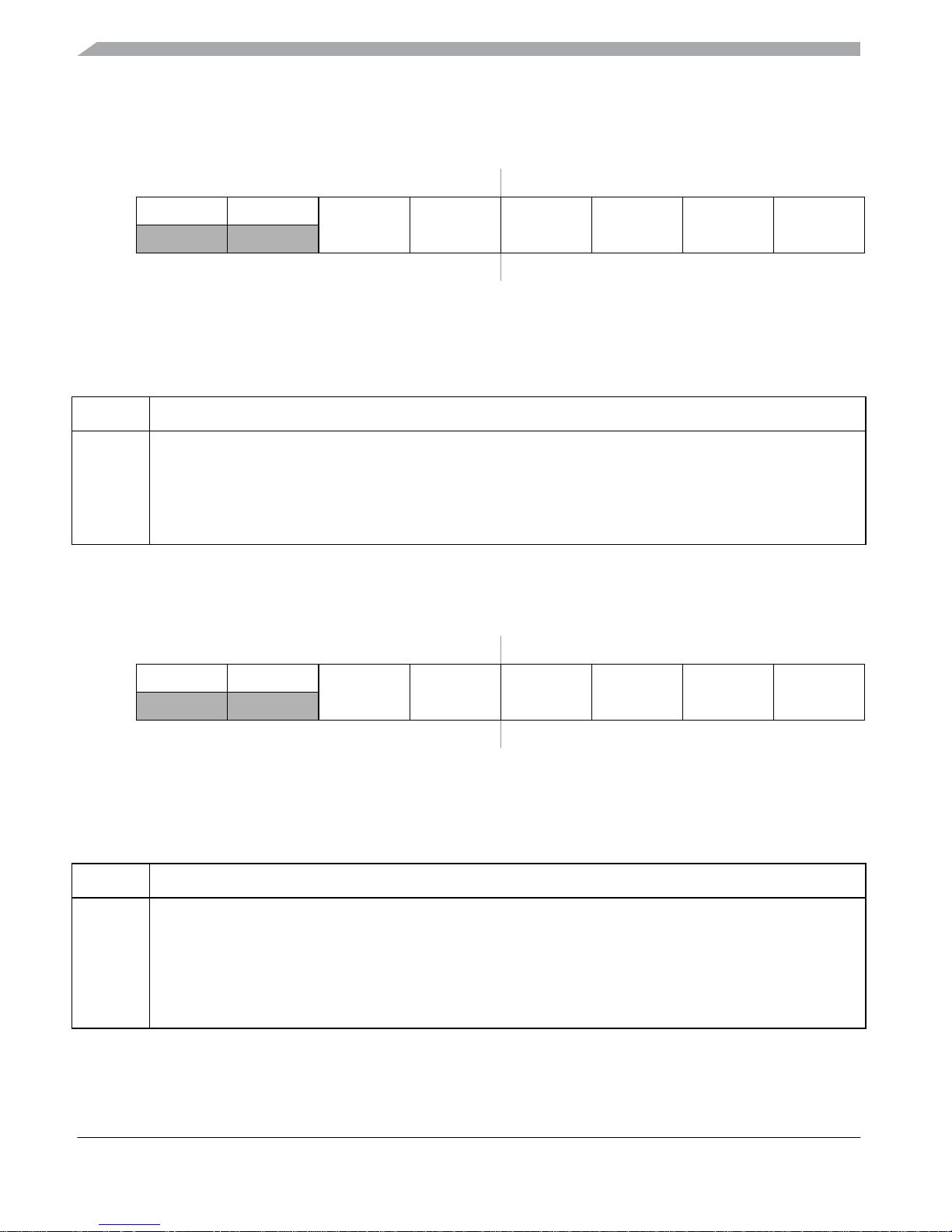
Port Integration Module (S12VRPIMV2)
MC9S12VR Family Reference Manual, Rev. 2.2
88 Freescale Semiconductor
Preliminary - Subject to Change Without Notice
2.3.42 Port AD Pull Enable Register (PER1AD)
2.3.43 Port AD Polarity Select Register (PPS1AD)
Address 0x0279 Access: User read/write
1
1
Read: Anytime
Write: Anytime
76543210
R0 0
PER1AD5 PER1AD4 PER1AD3 PER1AD2 PER1AD1 PER1AD0
W
Reset 00000000
Figure 2-41. Port AD Pullup Enable Register (PER1AD)
Table 2-44. PER1AD Register Field Descriptions
Field Description
5-0
PER1AD
Pull device Enable Register 1 port AD — Enable pull device on input pin
This bit controls whether a pull device on the associated port input pin is active. If a pin is used as output this bit has
no effect. The polarity is selected by the related polarity select register bit.
1 Pull device enabled
0 Pull device disabled
Address 0x027B Access: User read/write
1
1
Read: Anytime
Write: Anytime
76543210
R0 0
PPS1AD5 PPS1AD4 PPS1AD3 PPS1AD2 PPS1AD1 PPS1AD0
W
Reset 00000000
Figure 2-42. Port AD Polarity Select Register (PPS1AD)
Table 2-45. PPS1AD Register Field Descriptions
Field Description
5-0
PPS1AD
Pull device Polarity Select register 1 port AD — Configure pull device polarity and pin interrupt edge polarity on
input pin
This bit selects a pullup or a pulldown device if enabled on the associated port input pin.
This bit also selects the polarity of the active pin interrupt edge.
1 A pulldown device is selected; rising edge selected
0 A pullup device is selected; falling edge selected
Downloaded from Elcodis.com electronic components distributor
Page 89
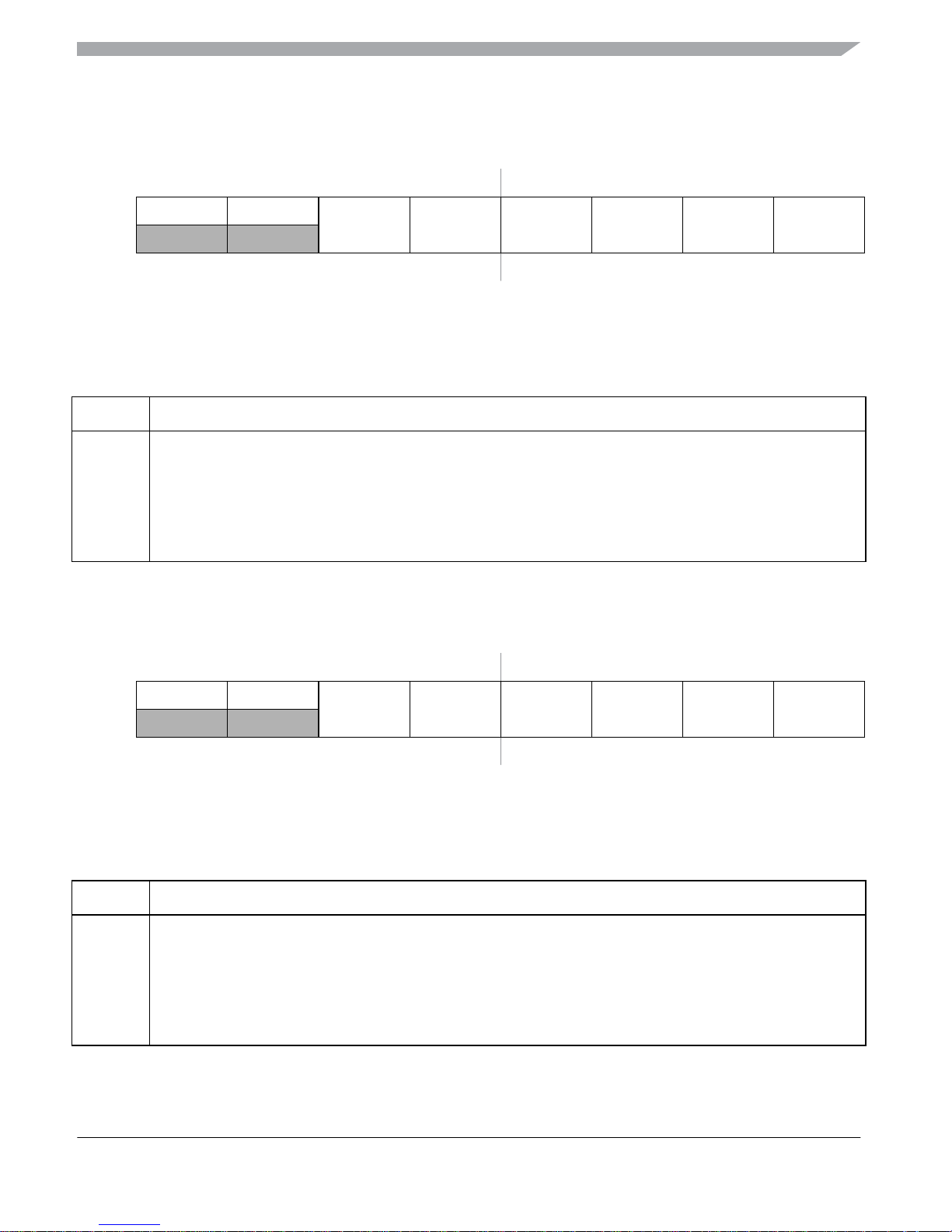
Port Integration Module (S12VRPIMV2)
MC9S12VR Family Reference Manual, Rev. 2.2
Freescale Semiconductor 89
Preliminary - Subject to Change Without Notice
2.3.44 Port AD Interrupt Enable Register (PIE1AD)
Read: Anytime.
2.3.45 Port AD Interrupt Flag Register (PIF1AD)
Address 0x027D Access: User read/write
1
1
Read: Anytime
Write: Anytime
76543210
R0 0
PIE1AD5 PIE1AD4 PIE1AD3 PIE1AD2 PIE1AD1 PIE1AD0
W
Reset 00000000
Figure 2-43. Port AD Interrupt Enable Register (PIE1AD)
Table 2-46. PIE1AD Register Field Descriptions
Field Description
5-0
PIE1AD
Pin Interrupt Enable register 1 port AD —
This bit enables or disables the edge sensitive pin interrupt on the associated pin. An interrupt can be generated if
the pin is operating in input or output mode when in use with the general-purpose or related peripheral function.
For wakeup from stop mode this bit must be set to allow activating the RC oscillator.
1 Interrupt is enabled
0 Interrupt is disabled (interrupt flag masked)
Address 0x027F Access: User read/write
1
1
Read: Anytime
Write: Anytime, write 1 to clear
76543210
R0 0
PIF1AD5 PIF1AD4 PIF1AD3 PIF1AD2 PIF1AD1 PIF1AD0
W
Reset 00000000
Figure 2-44. Port AD Interrupt Flag Register (PIF1AD)
Table 2-47. PIF1AD Register Field Descriptions
Field Description
5-0
PIF1AD
Pin Interrupt Flag register 1 port AD —
This flag asserts after a valid active edge was detected on the related pin (Section 2.4.4, “Interrupts”). This can be
a rising or a falling edge based on the state of the polarity select register. An interrupt will occur if the associated
interrupt enable bit is set.
1 Active edge on the associated bit has occurred
0 No active edge occurred
Downloaded from Elcodis.com electronic components distributor
Page 90
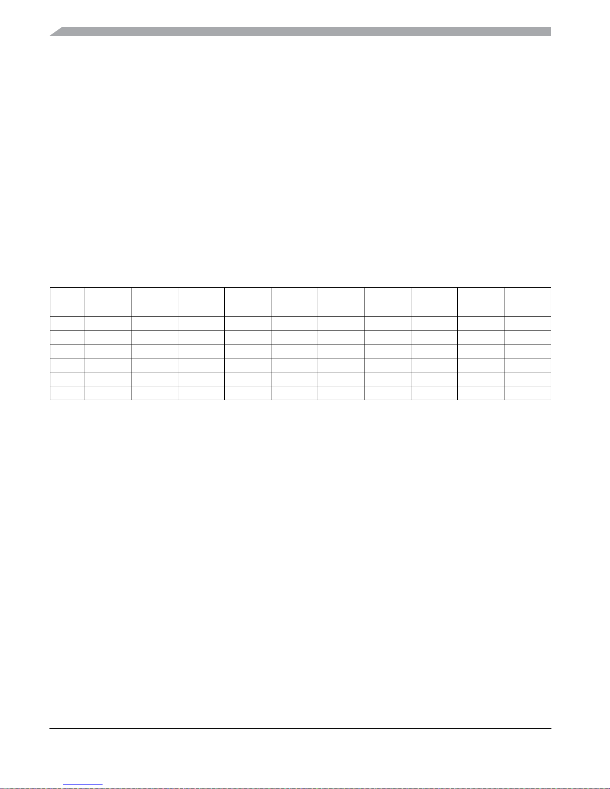
Port Integration Module (S12VRPIMV2)
MC9S12VR Family Reference Manual, Rev. 2.2
90 Freescale Semiconductor
Preliminary - Subject to Change Without Notice
2.4 Functional Description
2.4.1 General
Each pin except BKGD and port L pins can act as general-purpose I/O. In addition each pin can act as an
output or input of a peripheral module.
2.4.2 Registers
Table 2-48 lists the configuration registers which are available on each port. These registers except the pin
input and routing registers can be written at any time, however a specific configuration might not become
active.
For example selecting a pullup device: This device does not become active while the port is used as a
push-pull output.
2.4.2.1 Data register (PTx)
This register holds the value driven out to the pin if the pin is used as a general-purpose I/O.
Writing to this register has only an effect on the pin if the pin is used as general-purpose output. When
reading this address, the synchronized state of the pin is returned if the associated data direction register
bit is set to “0”.
If the data direction register bits are set to logic level “1”, the contents of the data register is returned. This
is independent of any other configuration (Figure 2-45).
2.4.2.2 Input register (PTIx)
This register is read-only and always returns the synchronized state of the pin (Figure 2-45).
2.4.2.3 Data direction register (DDRx)
This register defines whether the pin is used as an general-purpose input or an output.
If a peripheral module controls the pin the contents of the data direction register is ignored (Figure 2-45).
Table 2-48. Register availability per port
1
1
Each cell represents one register with individual configuration bits
Port Data Input
Data
Direction
Reduced
Drive
Pull
Enable
Polarity
Select
Wired-
Or Mode
Interrupt
Enable
Interrupt
Flag
Routing
Eyes-yes-yes-----
T yes yes yes - yes yes - - - yes
S yes yes yes - yes yes yes - - yes
P yes yes yes yes yes yes - yes yes -
L- yesyes
2
2
Input buffer control only
- - yes - yes yes -
AD yes yes yes - yes yes - yes yes -
Downloaded from Elcodis.com electronic components distributor
Page 91
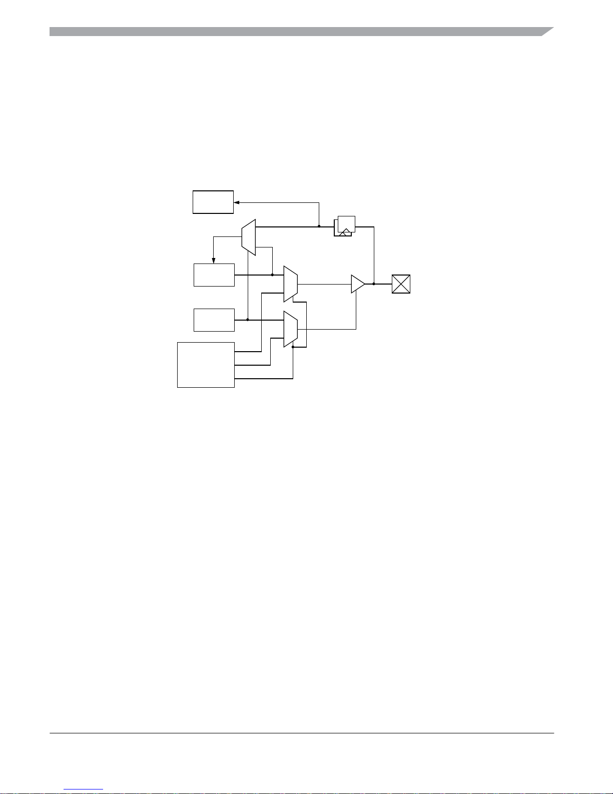
Port Integration Module (S12VRPIMV2)
MC9S12VR Family Reference Manual, Rev. 2.2
Freescale Semiconductor 91
Preliminary - Subject to Change Without Notice
Independent of the pin usage with a peripheral module this register determines the source of data when
reading the associated data register address (2.4.2.1/2-90).
NOTE
Due to internal synchronization circuits, it can take up to 2 bus clock cycles
until the correct value is read on port data or port input registers, when
changing the data direction register.
Figure 2-45. Illustration of I/O pin functionality
2.4.2.4 Reduced drive register (RDRx)
If the pin is used as an output this register allows the configuration of the drive strength independent of the
use with a peripheral module.
2.4.2.5 Pull device enable register (PERx)
This register turns on a pullup or pulldown device on the related pins determined by the associated polarity
select register (2.4.2.6/2-91).
The pull device becomes active only if the pin is used as an input or as a wired-or output. Some peripheral
module only allow certain configurations of pull devices to become active. Refer to the respective bit
descriptions.
2.4.2.6 Polarity select register (PPSx)
This register selects either a pullup or pulldown device if enabled.
It becomes only active if the pin is used as an input. A pullup device can be activated if the pin is used as
a wired-or output.
PT
DDR
output enable
module enable
1
0
1
1
0
0
PIN
PTI
data out
Module
Downloaded from Elcodis.com electronic components distributor
Page 92

Port Integration Module (S12VRPIMV2)
MC9S12VR Family Reference Manual, Rev. 2.2
92 Freescale Semiconductor
Preliminary - Subject to Change Without Notice
2.4.2.7 Wired-or mode register (WOMx)
If the pin is used as an output this register turns off the active-high drive. This allows wired-or type
connections of outputs.
2.4.2.8 Interrupt enable register (PIEx)
If the pin is used as an interrupt input this register serves as a mask to the interrupt flag to enable/disable
the interrupt.
2.4.2.9 Interrupt flag register (PIFx)
If the pin is used as an interrupt input this register holds the interrupt flag after a valid pin event.
2.4.2.10 Module routing register (MODRRx)
Routing registers allow software re-configuration of specific peripheral inputs and outputs:
• MODRR0 selects the driving source of the HSDRV and LSDRV pins
• MODRR1 selects optional pins for PWM channels and ETRIG inputs
• MODRR2 supports options to test the internal SCI-LINPHY interface signals
2.4.3 Pins and Ports
NOTE
Please refer to the device pinout section to determine the pin availability in
the different package options.
2.4.3.1 BKGD pin
The BKGD pin is associated with the BDM module.
During reset, the BKGD pin is used as MODC input.
2.4.3.2 Port E
This port is associated with the CPMU OSC.
Port E pins PE1-0 can be used for general-purpose or with the CPMU OSC module.
2.4.3.3 Port T
This port is associated with TIM, routed SCI-LINPHY interface and routed SPI.
Port T pins can be used for either general-purpose I/O or with the channels of the standard TIM, SPI, or
SCI and LINPHY subsystems.
Downloaded from Elcodis.com electronic components distributor
Page 93

Port Integration Module (S12VRPIMV2)
MC9S12VR Family Reference Manual, Rev. 2.2
Freescale Semiconductor 93
Preliminary - Subject to Change Without Notice
2.4.3.4 Port S
This port is associated with the ECLK, SPI, SCI1, routed SCI0, routed PWM channels and ETRIG inputs.
Port S pins can be used either for general-purpose I/O, or with the ECLK, SPI, SCI, and PWM subsystems.
2.4.3.5 Port P
Port P pins can be used for either general-purpose I/O, IRQ and XIRQ or with the PWM subsystem. All
pins feature pin interrupt functionality.
PP2 has an increased current capability to drive up to 20 mA to supply external devices for external Hall
sensors. An over-current protection is available.
PP1 and PP0 have an increased current capability to drive up to 10 mA.
PP4 and PP5 support ETRIG functionality.
PP5 can be used for either general-purpose input or as the level- or falling edge-sensitive
IRQ interrupt
input.
IRQ will be enabled by setting the IRQCR[IRQEN] configuration bit (2.3.8/2-59) and clearing the
I-bit in the CPU condition code register. It is inhibited at reset so this pin is initially configured as a simple
input with a pullup.
PP0 can be used for either general-purpose input or as the level-sensitive XIRQ interrupt input. XIRQ can
be enabled by clearing the X-bit in the CPU condition code register. It is inhibited at reset so this pin is
initially configured as a high-impedance input with a pullup.
2.4.3.6 Port L
Port L provides four high-voltage inputs (HVI) with the following features:
• Input voltage proof up to V
HVIx
• Digital input function with pin interrupt and wakeup from stop capability
• Analog input function with selectable divider ratio routable to ADC channel. Optional direct input
bypassing voltage divider and impedance converter. Capable to wakeup from stop (pin interrupts
in run mode not available). Open input detection.
Figure 2-46 shows a block diagram of the HVI.
Downloaded from Elcodis.com electronic components distributor
Page 94
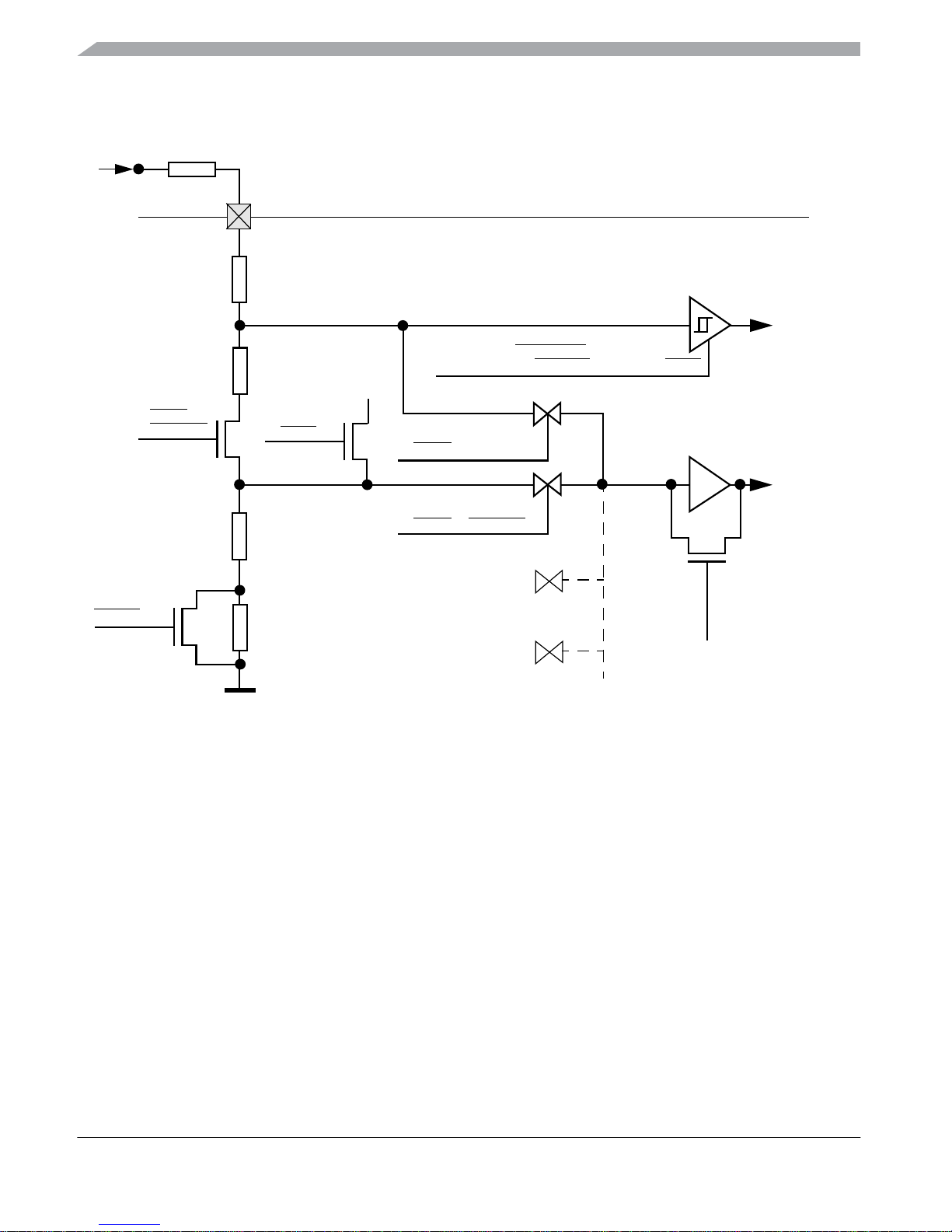
Port Integration Module (S12VRPIMV2)
MC9S12VR Family Reference Manual, Rev. 2.2
94 Freescale Semiconductor
Preliminary - Subject to Change Without Notice
Figure 2-46. HVI Block Diagram
Voltages up to V
HVIx
can be applied to all HVI pins. Internal voltage dividers scale the input signals down
to logic level. There are two modes, digital and analog, where these signals can be processed.
2.4.3.6.1 Digital Mode Operation
In digital mode the input buffers are enabled (DIENL[x]=1 & PTAL[PTAENL]=0). The synchronized pin
input state determined at threshold level V
TH_HVI
can be read in register PTIL. Interrupt flags (PIFL) are
set on input transitions if enabled (PIEL[x]=1) and configured for the related edge polarity (PPSL).
Wakeup from stop mode is supported.
2.4.3.6.2 Analog Mode Operation
In analog mode (PTAL[PTAENL]=1) the voltage applied to a selectable pin (PTAL[PTAL1:PTAL0]) can
be measured on an internal ADC channel (refer to device overview section for channel assignment). One
of two input divider ratios (Ratio
H_HVI
, Ratio
L_HVI
) can be chosen on each analog input (PIRL[x]) or the
HVIx
PTIL[x]
PIRL[x]
ADC
R
EXT_HVI
ANALOG[x]
V
HVI
(DIENL[x] & (ANALOG[x] | STOP))
Input Buffer
Impedance
Converter
PTAENL
&
STOP & PTADIRL
ANALOG[x]
& STOP & PTADIRL
VDDX
& STOP
ANALOG[x]
| (ANALOG[x] & PTADIRL & PTTEL & STOP)
40K
500K
110K
440K
ANALOG[x] = PTAENL & PTAL[1:0]
ANALOG[x]
& PTTEL
& PTPSL
& PTADIRL
& PTABYPL
(other inputs)
10K
& PTADIRL
& STOP
Downloaded from Elcodis.com electronic components distributor
Page 95
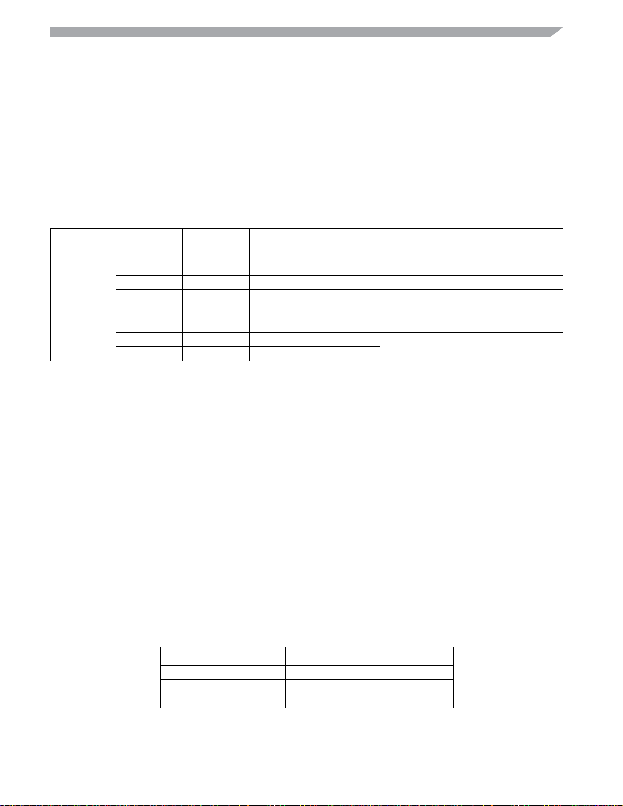
Port Integration Module (S12VRPIMV2)
MC9S12VR Family Reference Manual, Rev. 2.2
Freescale Semiconductor 95
Preliminary - Subject to Change Without Notice
voltage divider can be bypassed (PTAL[PTADIRL]=1). Additionally in latter case the impedance
converter in the ADC signal path can be configured to be used or bypassed in direct input mode
(PTAL[PTABYPL]).
In run mode the digital input buffer of the selected pin is disabled to avoid shoot-through current. Thus pin
interrupts cannot be generated.
In stop mode the digital input buffer is enabled only if DIENL[x]=1 to support wakeup functionality.
Table 2-49 shows the HVI input configuration depending on register bits and operation mode.
NOTE
An external resistor R
EXT_HVI
must always be connected to the
high-voltage inputs to protect the device pins from fast transients and to
achieve the specified pin input divider ratios when using the HVI in analog
mode.
2.4.3.7 Port AD
This port is associated with the ADC.
Port AD pins can be used for either general-purpose I/O, or with the ADC subsystem.
2.4.4 Interrupts
This section describes the interrupts generated by the PIM and their individual sources. Vector addresses
and interrupt priorities are defined at MCU level.
Table 2-49. HVI Input Configurations
Mode DIENL PTAENL Digital Input Analog Input Resulting Function
Run 0 0 off off Input disabled (Reset)
0 1 off
1
enabled Analog input, interrupt not supported
1 0 enabled off Digital input, interrupt supported
1 1 off
1
1
Enabled if (PTAL[PTTEL]=1 & PTAL[PTADIRL]=0)
enabled Analog input, interrupt not supported
Stop 0 0 off off Input disabled, wakeup from stop not
supported
0 1 off off
1 0 enabled off Digital input, wakeup from stop supported
1 1 enabled off
Table 2-50. PIM Interrupt Sources
Module Interrupt Sources Local Enable
XIRQ None
IRQ IRQCR[IRQEN]
Port P pin interrupt PIEP[PIEP5-PIEP0]
Downloaded from Elcodis.com electronic components distributor
Page 96

Port Integration Module (S12VRPIMV2)
MC9S12VR Family Reference Manual, Rev. 2.2
96 Freescale Semiconductor
Preliminary - Subject to Change Without Notice
2.4.4.1 XIRQ, IRQ Interrupts
The XIRQ pin allows requesting non-maskable interrupts after reset initialization. During reset, the X bit
in the condition code register is set and any interrupts are masked until software enables them.
The
IRQ pin allows requesting asynchronous interrupts. The interrupt input is disabled out of reset. To
enable the interrupt the IRQCR[IRQEN] bit must be set and the I bit cleared in the condition code register.
The interrupt can be configured for level-sensitive or falling-edge-sensitive triggering. If IRQCR[IRQEN]
is cleared while an interrupt is pending, the request will deassert.
Both interrupts are capable to wake-up the device from stop mode. Means for glitch filtering are not
provided on these pins.
2.4.4.2 Pin Interrupts and Wakeup
Ports P, L and AD offer pin interrupt capability. The related interrupt enable (PIE) as well as the sensitivity
to rising or falling edges (PPS) can be individually configured on per-pin basis. All bits/pins in a port share
the same interrupt vector. Interrupts can be used with the pins configured as inputs or outputs.
An interrupt is generated when a bit in the port interrupt flag (PIF) and its corresponding port interrupt
enable (PIE) are both set. The pin interrupt feature is also capable to wake up the CPU when it is in stop
or wait mode.
A digital filter on each pin prevents short pulses from generating an interrupt. A valid edge on an input is
detected if 4 consecutive samples of a passive level are followed by 4 consecutive samples of an active
level. Else the sampling logic is restarted.
In run and wait mode the filters are continuously clocked by the bus clock. Pulses with a duration of t
PULSE
<n
P_MASK/fbus
are assuredly filtered out while pulses with a duration of t
PULSE>nP_PASS/fbus
guarantee
a pin interrupt.
In stop mode the clock is generated by an RC-oscillator. The minimum pulse length varies over process
conditions, temperature and voltage (Figure 2-47). Pulses with a duration of t
PULSE
< t
P_MASK
are
assuredly filtered out while pulses with a duration of t
PULSE
> t
P_PASS
guarantee a wakeup event.
Please refer to the appendix table “Pin Interrupt Characteristics” for pulse length limits.
To maximize current saving the RC oscillator is active only if the following condition is true on any
individual pin:
Sample count <= 4 (at active or passive level) and interrupt enabled (PIE[x]=1) and interrupt flag not set
(PIF[x]=0).
Port L pin interrupt PIEL[PIEL3-PIEL0]
Port AD pin interrupt PIE1AD[PIE1AD5-PIE1AD0]
Port P over-current PIEP[OCIE]
Table 2-50. PIM Interrupt Sources
Module Interrupt Sources Local Enable
Downloaded from Elcodis.com electronic components distributor
Page 97
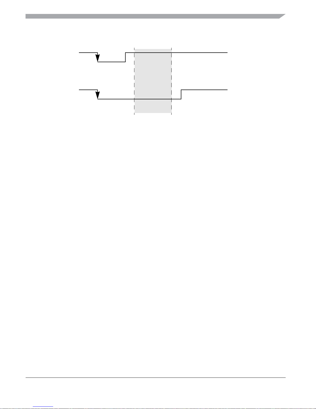
Port Integration Module (S12VRPIMV2)
MC9S12VR Family Reference Manual, Rev. 2.2
Freescale Semiconductor 97
Preliminary - Subject to Change Without Notice
Figure 2-47. Interrupt Glitch Filter (here: active low level selected)
2.4.4.3 Over-Current Interrupt
In case of an over-current condition on PP2 (see Section 2.5.3, “Over-Current Protection on EVDD”) the
over-current interrupt flag PIFP[OCIF] asserts. This flag generates an interrupt if the enable bit
PIEP[OCIE] is set.
An asserted flag immediately forces the output pin low to protect the device. The flag must be cleared to
re-enable the driver.
2.5 Initialization and Application Information
2.5.1 Port Data and Data Direction Register writes
It is not recommended to write PORT[x]/PT[x] and DDR[x] in a word access. When changing the register
pins from inputs to outputs, the data may have extra transitions during the write access. Initialize the port
data register before enabling the outputs.
2.5.2 ADC External Triggers ETRIG1-0
The ADC external trigger inputs ETRIG1-0 allow the synchronization of conversions to external trigger
events if selected as trigger source (for details refer to ATDCTL1[ETRIGSEL] and ATDCTL1[ETRIGCH]
configuration bits in ADC section). These signals are related to PWM channels 5-4 to support periodic
trigger applications with the ADC. Other pin functions can also be used as triggers.
If a PWM channel is routed to an alternative pin, the ETRIG input function will follow the relocation
accordingly.
If the related PWM channel is enabled and not routed for internal use, the PWM signal as seen on the pin
will drive the ETRIG input. Else the ETRIG function will be triggered by other functions on the pin
including general-purpose input.
Glitch, filtered out, no interrupt flag set
Valid pulse, interrupt flag set
uncertain
t
PULSE
(min)
t
PULSE
(max)
Downloaded from Elcodis.com electronic components distributor
Page 98

Port Integration Module (S12VRPIMV2)
MC9S12VR Family Reference Manual, Rev. 2.2
98 Freescale Semiconductor
Preliminary - Subject to Change Without Notice
2.5.3 Over-Current Protection on EVDD
Pin PP2 can be used as general-purpose I/O or due to its increased current capability in output mode as a
switchable external power supply pin (EVDD) for external devices like Hall sensors. An over-current
monitor is implemented to protect the controller from short circuits or excess currents on the output which
can only arise if the pin is configured for full drive. Although the full drive current is available on the high
and low side, the protection is only available if the pin is driven high (PTP[PTP2]=1). This is also true if
using the pin with the PWM.
To power up the over-current monitor set PIMMISC[OCPE]=1.
In stop mode the over-current monitor is disabled for power saving. The increased current capability
cannot be maintained to supply the external device. Therefore when using the pin as power supply the
external load must be powered down prior to entering stop mode by setting PTP[PTP2]=0.
An over-current condition is detected if the output current level exceeds the threshold I
OCD
in run mode.
The output driver is immediately forced low and the over-current interrupt flag PIFP[OCIF] asserts. Refer
to Section 2.4.4.3, “Over-Current Interrupt”.
2.5.4 Open Input Detection on HVI Pins
The connection of an external pull device on any port L high-voltage input can be validated by using the
built-in pull functionality of the HVI pins. Depending on the application type an external pulldown circuit
can be detected with the internal pullup device whereas an external pullup circuit can be detected with the
internal pulldown device which is part of the input voltage divider.
Note that the following procedures make use of a function that overrides the automatic disable mechanism
of the digital input buffers when using the inputs in analog mode. Make sure to switch off the override
function when using an input in analog mode after the check has been completed.
External pulldown device (Figure 2-48):
1. Enable analog function on HVIx in non-direct mode (PTAL[PTAENL]=1, PTAL[PTADIRL]=0,
PTAL[PTAL1:PTAL0]=x, where x is 0, 1, 2, or 3)
2. Select internal pullup device on selected HVI (PTAL[PTPSL]=1)
3. Enable function to force input buffer active on selected HVI in analog mode (PTAL[PTTEL]=1)
4. Verify PTILx=0 for a connected external pulldown device; read PTILx=1 for an open input
Downloaded from Elcodis.com electronic components distributor
Page 99
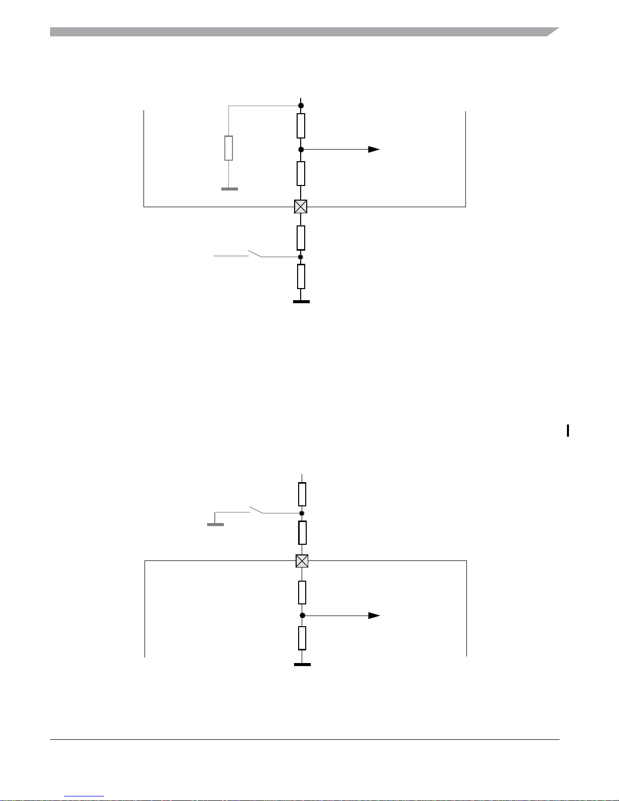
Port Integration Module (S12VRPIMV2)
MC9S12VR Family Reference Manual, Rev. 2.2
Freescale Semiconductor 99
Preliminary - Subject to Change Without Notice
Figure 2-48. Digital Input Read with Pullup Enabled
External pullup device (Figure 2-49):
1. Enable analog function on HVIx in non-direct mode (PTAL[PTAENL]=1, PTAL[PTADIRL]=0,
PTAL[PTAL1:PTAL0]=x, where x is 0, 1, 2, or 3)
2. Select internal pulldown device on selected HVI (PTAL[PTPSL]=0)
3. Enable function to force input buffer active on selected HVI in analog mode (PTAL[PTTEL]=1)
4. Verify PTILx=1 for a connected external pullup device; read PTILx=0 for an open input
Figure 2-49. Digital Input Read with Pulldown Enabled
HVIx
40K
500K
VDDX
Digital in
110K / 550K
min. 1/10 * V
DDX
10K
PIRL=0 / PIRL=1
HV Supply
HVIx
40K
610K / 1050K
Digital in
max. 10/11 * V
HVI
(PIRL=0)
PIRL=0 / PIRL=1
max. 21/22 * V
HVI
(PIRL=1)
10K
HV Supply
Downloaded from Elcodis.com electronic components distributor
Page 100

Port Integration Module (S12VRPIMV2)
MC9S12VR Family Reference Manual, Rev. 2.2
100 Freescale Semiconductor
Preliminary - Subject to Change Without Notice
Downloaded from Elcodis.com electronic components distributor
 Loading...