


MC9S12C Family
MC9S12GC Family
Reference Manual
HCS12
Microcontrollers
MC9S12C128
Rev 01.24
05/2010
freescale.com
To provide the most up-to-date information, the revision of our documents on the World Wide Web will be
the most current. Your printed copy may be an earlier revision. To verify you have the latest information
available, refer to:
http://freescale.com/
A full list of family members and options is included in the appendices.
The following revision history table summarizes changes contained in this document.
This document contains information for all constituent modules, with the exception of the S12 CPU. For
S12 CPU information please refer to the CPU S12 Reference Manual.
Revision History
Date
June, 2005 01.14 New Book
July, 2005 01.15
Oct, 2005 01.16
Dec, 2005 01.17 Added note to PIM block diagram figure
Dec, 2005 01.18 Added PIM rerouting information to 80-pin package diagram
Jan, 2006 01.19
Mar, 2006 01.20 Cleaned up Device Overview Section
May, 2006 01.21
Dec, 2006 01.22
May, 2007 01.23
Revision
Level
Description
Removed 16MHz option for 128K, 96K and 64K versions
Minor corrections following review
Added outstanding flash module descriptions
Added EPP package options
Corrected and Enhanced recommended PCB layouts
Modified LVI levels in electrical parameter section
Corrected TSCR2 typo in timer register listing
Added 0M66G to PartID table
Added units to MSCAN timing parameter table
Corrected missing overbars on pin names
Corrected CRGFLG contents in register summary
Removed non existing part number options
Removed unintended symbol fonts from table A6
Updated ATD section
Corrected typos
May, 2010 01.24 Updated TIM section

Chapter 1 MC9S12C and MC9S12GC Device Overview (MC9S12C128) .17
Chapter 2 Port Integration Module (PIM9C32) . . . . . . . . . . . . . . . . . . . . .73
Chapter 3 Module Mapping Control (MMCV4) . . . . . . . . . . . . . . . . . . . .109
Chapter 4 Multiplexed External Bus Interface (MEBIV3) . . . . . . . . . . . .129
Chapter 5 Interrupt (INTV1) . . . . . . . . . . . . . . . . . . . . . . . . . . . . . . . . . . .157
Chapter 6 Background Debug Module (BDMV4) . . . . . . . . . . . . . . . . . .165
Chapter 7 Debug Module (DBGV1) . . . . . . . . . . . . . . . . . . . . . . . . . . . . .191
Chapter 8 Analog-to-Digital Converter (ATD10B8C) . . . . . . . . . . . . . . .223
Chapter 9 Clocks and Reset Generator (CRGV4) . . . . . . . . . . . . . . . . . .251
Chapter 10 Scalable Controller Area Network (S12MSCANV2) . . . . . . . . 287
Chapter 11 Oscillator (OSCV2) . . . . . . . . . . . . . . . . . . . . . . . . . . . . . . . . .343
Chapter 12 Pulse-Width Modulator (PWM8B6CV1) . . . . . . . . . . . . . . . . .347
Chapter 13 Serial Communications Interface (S12SCIV2) . . . . . . . . . . . .383
Chapter 14 Serial Peripheral Interface (SPIV3) . . . . . . . . . . . . . . . . . . . . .413
Chapter 15 Timer Module (TIM16B8CV1) . . . . . . . . . . . . . . . . . . . . . . . . .435
Chapter 16 Dual Output Voltage Regulator (VREG3V3V2) . . . . . . . . . . .463
Chapter 17 16 Kbyte Flash Module (S12FTS16KV1) . . . . . . . . . . . . . . . . . 471
Chapter 18 32 Kbyte Flash Module (S12FTS32KV1) . . . . . . . . . . . . . . . . . 503
Chapter 19 64 Kbyte Flash Module (S12FTS64KV4) . . . . . . . . . . . . . . . . . 537
Chapter 20 96 Kbyte Flash Module (S12FTS96KV1) . . . . . . . . . . . . . . . . . 575
Chapter 21 128 Kbyte Flash Module (S12FTS128K1V1) . . . . . . . . . . . . . . 613
Appendix A Electrical Characteristics. . . . . . . . . . . . . . . . . . . . . . . . . . . . .647
Appendix B Emulation Information . . . . . . . . . . . . . . . . . . . . . . . . . . . . . . .679
Appendix C Package Information . . . . . . . . . . . . . . . . . . . . . . . . . . . . . . . . 681
Appendix D Derivative Differences . . . . . . . . . . . . . . . . . . . . . . . . . . . . . . .685
Freescale Semiconductor MC9S12C-Family / MC9S12GC-Family 3
Rev 01.24

Appendix E Ordering Information . . . . . . . . . . . . . . . . . . . . . . . . . . . . . . . .686
4 MC9S12C-Family / MC9S12GC-Family Freescale Semiconductor
Rev 01.24

Chapter 1
MC9S12C and MC9S12GC Device Overview (MC9S12C128)
1.1 Introduction . . . . . . . . . . . . . . . . . . . . . . . . . . . . . . . . . . . . . . . . . . . . . . . . . . . . . . . . . . . . . . . . . . 17
1.1.1 Features . . . . . . . . . . . . . . . . . . . . . . . . . . . . . . . . . . . . . . . . . . . . . . . . . . . . . . . . . . . . . . 17
1.1.2 Modes of Operation . . . . . . . . . . . . . . . . . . . . . . . . . . . . . . . . . . . . . . . . . . . . . . . . . . . . .19
1.1.3 Block Diagram . . . . . . . . . . . . . . . . . . . . . . . . . . . . . . . . . . . . . . . . . . . . . . . . . . . . . . . . . 20
1.2 Memory Map and Registers . . . . . . . . . . . . . . . . . . . . . . . . . . . . . . . . . . . . . . . . . . . . . . . . . . . . . . 21
1.2.1 Device Memory Map . . . . . . . . . . . . . . . . . . . . . . . . . . . . . . . . . . . . . . . . . . . . . . . . . . . . 21
1.2.2 Detailed Register Map . . . . . . . . . . . . . . . . . . . . . . . . . . . . . . . . . . . . . . . . . . . . . . . . . . . 27
1.2.3 Part ID Assignments . . . . . . . . . . . . . . . . . . . . . . . . . . . . . . . . . . . . . . . . . . . . . . . . . . . .44
1.3 Signal Description . . . . . . . . . . . . . . . . . . . . . . . . . . . . . . . . . . . . . . . . . . . . . . . . . . . . . . . . . . . . . 45
1.3.1 Device Pinouts . . . . . . . . . . . . . . . . . . . . . . . . . . . . . . . . . . . . . . . . . . . . . . . . . . . . . . . . . 45
1.3.2 Signal Properties Summary . . . . . . . . . . . . . . . . . . . . . . . . . . . . . . . . . . . . . . . . . . . . . . . 48
1.3.3 Pin Initialization for 48- and 52-Pin LQFP Bond Out Versions . . . . . . . . . . . . . . . . . . . 49
1.3.4 Detailed Signal Descriptions . . . . . . . . . . . . . . . . . . . . . . . . . . . . . . . . . . . . . . . . . . . . . . 50
1.3.5 Power Supply Pins . . . . . . . . . . . . . . . . . . . . . . . . . . . . . . . . . . . . . . . . . . . . . . . . . . . . . .55
1.4 System Clock Description . . . . . . . . . . . . . . . . . . . . . . . . . . . . . . . . . . . . . . . . . . . . . . . . . . . . . . . 57
1.5 Modes of Operation . . . . . . . . . . . . . . . . . . . . . . . . . . . . . . . . . . . . . . . . . . . . . . . . . . . . . . . . . . . . 57
1.5.1 Chip Configuration Summary . . . . . . . . . . . . . . . . . . . . . . . . . . . . . . . . . . . . . . . . . . . . . 57
1.5.2 Security . . . . . . . . . . . . . . . . . . . . . . . . . . . . . . . . . . . . . . . . . . . . . . . . . . . . . . . . . . . . . . 58
1.5.3 Low-Power Modes . . . . . . . . . . . . . . . . . . . . . . . . . . . . . . . . . . . . . . . . . . . . . . . . . . . . . . 59
1.6 Resets and Interrupts . . . . . . . . . . . . . . . . . . . . . . . . . . . . . . . . . . . . . . . . . . . . . . . . . . . . . . . . . . . 60
1.6.1 Vectors . . . . . . . . . . . . . . . . . . . . . . . . . . . . . . . . . . . . . . . . . . . . . . . . . . . . . . . . . . . . . . . 60
1.6.2 Resets . . . . . . . . . . . . . . . . . . . . . . . . . . . . . . . . . . . . . . . . . . . . . . . . . . . . . . . . . . . . . . . . 62
1.7 Device Specific Information and Module Dependencies . . . . . . . . . . . . . . . . . . . . . . . . . . . . . . . . 62
1.7.1 PPAGE . . . . . . . . . . . . . . . . . . . . . . . . . . . . . . . . . . . . . . . . . . . . . . . . . . . . . . . . . . . . . . . 62
1.7.2 BDM Alternate Clock . . . . . . . . . . . . . . . . . . . . . . . . . . . . . . . . . . . . . . . . . . . . . . . . . . . 63
1.7.3 Extended Address Range Emulation Implications . . . . . . . . . . . . . . . . . . . . . . . . . . . . . 63
1.7.4 VREGEN . . . . . . . . . . . . . . . . . . . . . . . . . . . . . . . . . . . . . . . . . . . . . . . . . . . . . . . . . . . . . 64
1.7.5 V
DD1
, V
1.7.6 Clock Reset Generator And VREG Interface . . . . . . . . . . . . . . . . . . . . . . . . . . . . . . . . . 64
1.7.7 Analog-to-Digital Converter . . . . . . . . . . . . . . . . . . . . . . . . . . . . . . . . . . . . . . . . . . . . . . 64
1.7.8 MODRR Register Port T And Port P Mapping . . . . . . . . . . . . . . . . . . . . . . . . . . . . . . . . 64
1.7.9 Port AD Dependency On PIM And ATD Registers . . . . . . . . . . . . . . . . . . . . . . . . . . . . . 64
1.8 Recommended Printed Circuit Board Layout . . . . . . . . . . . . . . . . . . . . . . . . . . . . . . . . . . . . . . . . 65
DD2
, V
, V
SS1
SS2 . . . . . . . . . . . . . . . . . . . . . . . . . . . . . . . . . . . . . . . . . . . . . . . . . . . . . . . . . . . . . . 64
Chapter 2
Port Integration Module (PIM9C32) Block Description
2.1 Introduction . . . . . . . . . . . . . . . . . . . . . . . . . . . . . . . . . . . . . . . . . . . . . . . . . . . . . . . . . . . . . . . . . . 73
2.1.1 Features . . . . . . . . . . . . . . . . . . . . . . . . . . . . . . . . . . . . . . . . . . . . . . . . . . . . . . . . . . . . . . 73
Freescale Semiconductor MC9S12C-Family / MC9S12GC-Family 5
Rev 01.24

2.1.2 Block Diagram . . . . . . . . . . . . . . . . . . . . . . . . . . . . . . . . . . . . . . . . . . . . . . . . . . . . . . . . . 74
2.2 Signal Description . . . . . . . . . . . . . . . . . . . . . . . . . . . . . . . . . . . . . . . . . . . . . . . . . . . . . . . . . . . . . 76
2.3 Memory Map and Registers . . . . . . . . . . . . . . . . . . . . . . . . . . . . . . . . . . . . . . . . . . . . . . . . . . . . . . 77
2.3.1 Module Memory Map . . . . . . . . . . . . . . . . . . . . . . . . . . . . . . . . . . . . . . . . . . . . . . . . . . . 77
2.3.2 Register Descriptions . . . . . . . . . . . . . . . . . . . . . . . . . . . . . . . . . . . . . . . . . . . . . . . . . . . .80
2.4 Functional Description . . . . . . . . . . . . . . . . . . . . . . . . . . . . . . . . . . . . . . . . . . . . . . . . . . . . . . . . . 104
2.4.1 Registers . . . . . . . . . . . . . . . . . . . . . . . . . . . . . . . . . . . . . . . . . . . . . . . . . . . . . . . . . . . . . 104
2.4.2 Port Descriptions . . . . . . . . . . . . . . . . . . . . . . . . . . . . . . . . . . . . . . . . . . . . . . . . . . . . . . 105
2.4.3 Port A, B, E and BKGD Pin . . . . . . . . . . . . . . . . . . . . . . . . . . . . . . . . . . . . . . . . . . . . . 107
2.4.4 External Pin Descriptions . . . . . . . . . . . . . . . . . . . . . . . . . . . . . . . . . . . . . . . . . . . . . . . 107
2.4.5 Low Power Options . . . . . . . . . . . . . . . . . . . . . . . . . . . . . . . . . . . . . . . . . . . . . . . . . . . . 107
2.5 Initialization Information . . . . . . . . . . . . . . . . . . . . . . . . . . . . . . . . . . . . . . . . . . . . . . . . . . . . . . . 107
2.5.1 Reset Initialization . . . . . . . . . . . . . . . . . . . . . . . . . . . . . . . . . . . . . . . . . . . . . . . . . . . . . 107
2.6 Interrupts . . . . . . . . . . . . . . . . . . . . . . . . . . . . . . . . . . . . . . . . . . . . . . . . . . . . . . . . . . . . . . . . . . . 108
2.6.1 Interrupt Sources . . . . . . . . . . . . . . . . . . . . . . . . . . . . . . . . . . . . . . . . . . . . . . . . . . . . . . 108
2.6.2 Recovery from STOP . . . . . . . . . . . . . . . . . . . . . . . . . . . . . . . . . . . . . . . . . . . . . . . . . . . 108
2.7 Application Information . . . . . . . . . . . . . . . . . . . . . . . . . . . . . . . . . . . . . . . . . . . . . . . . . . . . . . . . 108
Chapter 3
Module Mapping Control (MMCV4) Block Description
3.1 Introduction . . . . . . . . . . . . . . . . . . . . . . . . . . . . . . . . . . . . . . . . . . . . . . . . . . . . . . . . . . . . . . . . . 109
3.1.1 Features . . . . . . . . . . . . . . . . . . . . . . . . . . . . . . . . . . . . . . . . . . . . . . . . . . . . . . . . . . . . . 110
3.1.2 Modes of Operation . . . . . . . . . . . . . . . . . . . . . . . . . . . . . . . . . . . . . . . . . . . . . . . . . . . . 110
3.2 External Signal Description . . . . . . . . . . . . . . . . . . . . . . . . . . . . . . . . . . . . . . . . . . . . . . . . . . . . . 110
3.3 Memory Map and Register Definition . . . . . . . . . . . . . . . . . . . . . . . . . . . . . . . . . . . . . . . . . . . . . 110
3.3.1 Module Memory Map . . . . . . . . . . . . . . . . . . . . . . . . . . . . . . . . . . . . . . . . . . . . . . . . . . 110
3.3.2 Register Descriptions . . . . . . . . . . . . . . . . . . . . . . . . . . . . . . . . . . . . . . . . . . . . . . . . . . . 112
3.4 Functional Description . . . . . . . . . . . . . . . . . . . . . . . . . . . . . . . . . . . . . . . . . . . . . . . . . . . . . . . . . 122
3.4.1 Bus Control . . . . . . . . . . . . . . . . . . . . . . . . . . . . . . . . . . . . . . . . . . . . . . . . . . . . . . . . . . 122
3.4.2 Address Decoding . . . . . . . . . . . . . . . . . . . . . . . . . . . . . . . . . . . . . . . . . . . . . . . . . . . . . 122
3.4.3 Memory Expansion . . . . . . . . . . . . . . . . . . . . . . . . . . . . . . . . . . . . . . . . . . . . . . . . . . . . 124
Chapter 4
Multiplexed External Bus Interface (MEBIV3)
4.1 Introduction . . . . . . . . . . . . . . . . . . . . . . . . . . . . . . . . . . . . . . . . . . . . . . . . . . . . . . . . . . . . . . . . . 129
4.1.1 Features . . . . . . . . . . . . . . . . . . . . . . . . . . . . . . . . . . . . . . . . . . . . . . . . . . . . . . . . . . . . . 129
4.1.2 Modes of Operation . . . . . . . . . . . . . . . . . . . . . . . . . . . . . . . . . . . . . . . . . . . . . . . . . . . . 131
4.2 External Signal Description . . . . . . . . . . . . . . . . . . . . . . . . . . . . . . . . . . . . . . . . . . . . . . . . . . . . . 131
4.3 Memory Map and Register Definition . . . . . . . . . . . . . . . . . . . . . . . . . . . . . . . . . . . . . . . . . . . . . 133
4.3.1 Module Memory Map . . . . . . . . . . . . . . . . . . . . . . . . . . . . . . . . . . . . . . . . . . . . . . . . . . 134
4.3.2 Register Descriptions . . . . . . . . . . . . . . . . . . . . . . . . . . . . . . . . . . . . . . . . . . . . . . . . . . . 134
4.4 Functional Description . . . . . . . . . . . . . . . . . . . . . . . . . . . . . . . . . . . . . . . . . . . . . . . . . . . . . . . . . 150
4.4.1 Detecting Access Type from External Signals . . . . . . . . . . . . . . . . . . . . . . . . . . . . . . . . 150
4.4.2 Stretched Bus Cycles . . . . . . . . . . . . . . . . . . . . . . . . . . . . . . . . . . . . . . . . . . . . . . . . . . . 151
6 MC9S12C-Family / MC9S12GC-Family Freescale Semiconductor
Rev 01.24

4.4.3 Modes of Operation . . . . . . . . . . . . . . . . . . . . . . . . . . . . . . . . . . . . . . . . . . . . . . . . . . . . 151
4.4.4 Internal Visibility . . . . . . . . . . . . . . . . . . . . . . . . . . . . . . . . . . . . . . . . . . . . . . . . . . . . . . 156
4.4.5 Low-Power Options . . . . . . . . . . . . . . . . . . . . . . . . . . . . . . . . . . . . . . . . . . . . . . . . . . . . 156
Chapter 5
Interrupt (INTV1) Block Description
5.1 Introduction . . . . . . . . . . . . . . . . . . . . . . . . . . . . . . . . . . . . . . . . . . . . . . . . . . . . . . . . . . . . . . . . . 157
5.1.1 Features . . . . . . . . . . . . . . . . . . . . . . . . . . . . . . . . . . . . . . . . . . . . . . . . . . . . . . . . . . . . . 158
5.1.2 Modes of Operation . . . . . . . . . . . . . . . . . . . . . . . . . . . . . . . . . . . . . . . . . . . . . . . . . . . . 158
5.2 External Signal Description . . . . . . . . . . . . . . . . . . . . . . . . . . . . . . . . . . . . . . . . . . . . . . . . . . . . . 159
5.3 Memory Map and Register Definition . . . . . . . . . . . . . . . . . . . . . . . . . . . . . . . . . . . . . . . . . . . . . 159
5.3.1 Module Memory Map . . . . . . . . . . . . . . . . . . . . . . . . . . . . . . . . . . . . . . . . . . . . . . . . . . 159
5.3.2 Register Descriptions . . . . . . . . . . . . . . . . . . . . . . . . . . . . . . . . . . . . . . . . . . . . . . . . . . . 159
5.4 Functional Description . . . . . . . . . . . . . . . . . . . . . . . . . . . . . . . . . . . . . . . . . . . . . . . . . . . . . . . . . 161
5.4.1 Low-Power Modes . . . . . . . . . . . . . . . . . . . . . . . . . . . . . . . . . . . . . . . . . . . . . . . . . . . . . 162
5.5 Resets . . . . . . . . . . . . . . . . . . . . . . . . . . . . . . . . . . . . . . . . . . . . . . . . . . . . . . . . . . . . . . . . . . . . . . 162
5.6 Interrupts . . . . . . . . . . . . . . . . . . . . . . . . . . . . . . . . . . . . . . . . . . . . . . . . . . . . . . . . . . . . . . . . . . . 162
5.6.1 Interrupt Registers . . . . . . . . . . . . . . . . . . . . . . . . . . . . . . . . . . . . . . . . . . . . . . . . . . . . . 162
5.6.2 Highest Priority I-Bit Maskable Interrupt . . . . . . . . . . . . . . . . . . . . . . . . . . . . . . . . . . . 162
5.6.3 Interrupt Priority Decoder . . . . . . . . . . . . . . . . . . . . . . . . . . . . . . . . . . . . . . . . . . . . . . . 163
5.7 Exception Priority . . . . . . . . . . . . . . . . . . . . . . . . . . . . . . . . . . . . . . . . . . . . . . . . . . . . . . . . . . . . 163
Chapter 6
Background Debug Module (BDMV4) Block Description
6.1 Introduction . . . . . . . . . . . . . . . . . . . . . . . . . . . . . . . . . . . . . . . . . . . . . . . . . . . . . . . . . . . . . . . . . 165
6.1.1 Features . . . . . . . . . . . . . . . . . . . . . . . . . . . . . . . . . . . . . . . . . . . . . . . . . . . . . . . . . . . . . 165
6.1.2 Modes of Operation . . . . . . . . . . . . . . . . . . . . . . . . . . . . . . . . . . . . . . . . . . . . . . . . . . . . 166
6.2 External Signal Description . . . . . . . . . . . . . . . . . . . . . . . . . . . . . . . . . . . . . . . . . . . . . . . . . . . . . 167
6.2.1 BKGD — Background Interface Pin . . . . . . . . . . . . . . . . . . . . . . . . . . . . . . . . . . . . . . . 167
6.2.2
6.2.3
6.3 Memory Map and Register Definition . . . . . . . . . . . . . . . . . . . . . . . . . . . . . . . . . . . . . . . . . . . . . 168
6.3.1 Module Memory Map . . . . . . . . . . . . . . . . . . . . . . . . . . . . . . . . . . . . . . . . . . . . . . . . . . 168
6.3.2 Register Descriptions . . . . . . . . . . . . . . . . . . . . . . . . . . . . . . . . . . . . . . . . . . . . . . . . . . . 169
6.4 Functional Description . . . . . . . . . . . . . . . . . . . . . . . . . . . . . . . . . . . . . . . . . . . . . . . . . . . . . . . . . 174
6.4.1 Security . . . . . . . . . . . . . . . . . . . . . . . . . . . . . . . . . . . . . . . . . . . . . . . . . . . . . . . . . . . . . 174
6.4.2 Enabling and Activating BDM . . . . . . . . . . . . . . . . . . . . . . . . . . . . . . . . . . . . . . . . . . . 174
6.4.3 BDM Hardware Commands . . . . . . . . . . . . . . . . . . . . . . . . . . . . . . . . . . . . . . . . . . . . . 175
6.4.4 Standard BDM Firmware Commands . . . . . . . . . . . . . . . . . . . . . . . . . . . . . . . . . . . . . . 176
6.4.5 BDM Command Structure . . . . . . . . . . . . . . . . . . . . . . . . . . . . . . . . . . . . . . . . . . . . . . . 177
6.4.6 BDM Serial Interface . . . . . . . . . . . . . . . . . . . . . . . . . . . . . . . . . . . . . . . . . . . . . . . . . . . 179
6.4.7 Serial Interface Hardware Handshake Protocol . . . . . . . . . . . . . . . . . . . . . . . . . . . . . . . 182
6.4.8 Hardware Handshake Abort Procedure . . . . . . . . . . . . . . . . . . . . . . . . . . . . . . . . . . . . . 184
6.4.9 SYNC — Request Timed Reference Pulse . . . . . . . . . . . . . . . . . . . . . . . . . . . . . . . . . . 187
TAGHI — High Byte Instruction Tagging Pin . . . . . . . . . . . . . . . . . . . . . . . . . . . . . . . 167
TAGLO — Low Byte Instruction Tagging Pin . . . . . . . . . . . . . . . . . . . . . . . . . . . . . . . 167
Freescale Semiconductor MC9S12C-Family / MC9S12GC-Family 7
Rev 01.24

6.4.10 Instruction Tracing . . . . . . . . . . . . . . . . . . . . . . . . . . . . . . . . . . . . . . . . . . . . . . . . . . . . . 187
6.4.11 Instruction Tagging . . . . . . . . . . . . . . . . . . . . . . . . . . . . . . . . . . . . . . . . . . . . . . . . . . . . 188
6.4.12 Serial Communication Time-Out . . . . . . . . . . . . . . . . . . . . . . . . . . . . . . . . . . . . . . . . . . 188
6.4.13 Operation in Wait Mode . . . . . . . . . . . . . . . . . . . . . . . . . . . . . . . . . . . . . . . . . . . . . . . . . 189
6.4.14 Operation in Stop Mode . . . . . . . . . . . . . . . . . . . . . . . . . . . . . . . . . . . . . . . . . . . . . . . . . 189
Chapter 7
Debug Module (DBGV1) Block Description
7.1 Introduction . . . . . . . . . . . . . . . . . . . . . . . . . . . . . . . . . . . . . . . . . . . . . . . . . . . . . . . . . . . . . . . . . 191
7.1.1 Features . . . . . . . . . . . . . . . . . . . . . . . . . . . . . . . . . . . . . . . . . . . . . . . . . . . . . . . . . . . . . 191
7.1.2 Modes of Operation . . . . . . . . . . . . . . . . . . . . . . . . . . . . . . . . . . . . . . . . . . . . . . . . . . . . 193
7.1.3 Block Diagram . . . . . . . . . . . . . . . . . . . . . . . . . . . . . . . . . . . . . . . . . . . . . . . . . . . . . . . . 193
7.2 External Signal Description . . . . . . . . . . . . . . . . . . . . . . . . . . . . . . . . . . . . . . . . . . . . . . . . . . . . . 195
7.3 Memory Map and Register Definition . . . . . . . . . . . . . . . . . . . . . . . . . . . . . . . . . . . . . . . . . . . . . 196
7.3.1 Module Memory Map . . . . . . . . . . . . . . . . . . . . . . . . . . . . . . . . . . . . . . . . . . . . . . . . . . 196
7.3.2 Register Descriptions . . . . . . . . . . . . . . . . . . . . . . . . . . . . . . . . . . . . . . . . . . . . . . . . . . . 196
7.4 Functional Description . . . . . . . . . . . . . . . . . . . . . . . . . . . . . . . . . . . . . . . . . . . . . . . . . . . . . . . . . 212
7.4.1 DBG Operating in BKP Mode . . . . . . . . . . . . . . . . . . . . . . . . . . . . . . . . . . . . . . . . . . . . 212
7.4.2 DBG Operating in DBG Mode . . . . . . . . . . . . . . . . . . . . . . . . . . . . . . . . . . . . . . . . . . . 214
7.4.3 Breakpoints . . . . . . . . . . . . . . . . . . . . . . . . . . . . . . . . . . . . . . . . . . . . . . . . . . . . . . . . . . 221
7.5 Resets . . . . . . . . . . . . . . . . . . . . . . . . . . . . . . . . . . . . . . . . . . . . . . . . . . . . . . . . . . . . . . . . . . . . . . 222
7.6 Interrupts . . . . . . . . . . . . . . . . . . . . . . . . . . . . . . . . . . . . . . . . . . . . . . . . . . . . . . . . . . . . . . . . . . . 222
Chapter 8
Analog-to-Digital Converter (ATD10B8C)
Block Description
8.1 Introduction . . . . . . . . . . . . . . . . . . . . . . . . . . . . . . . . . . . . . . . . . . . . . . . . . . . . . . . . . . . . . . . . . 223
8.1.1 Features . . . . . . . . . . . . . . . . . . . . . . . . . . . . . . . . . . . . . . . . . . . . . . . . . . . . . . . . . . . . . 223
8.1.2 Modes of Operation . . . . . . . . . . . . . . . . . . . . . . . . . . . . . . . . . . . . . . . . . . . . . . . . . . . . 223
8.1.3 Block Diagram . . . . . . . . . . . . . . . . . . . . . . . . . . . . . . . . . . . . . . . . . . . . . . . . . . . . . . . . 224
8.2 Signal Description . . . . . . . . . . . . . . . . . . . . . . . . . . . . . . . . . . . . . . . . . . . . . . . . . . . . . . . . . . . . 225
8.2.1 AN7 / ETRIG / PAD7 . . . . . . . . . . . . . . . . . . . . . . . . . . . . . . . . . . . . . . . . . . . . . . . . . . 225
8.2.2 AN6 / PAD6 . . . . . . . . . . . . . . . . . . . . . . . . . . . . . . . . . . . . . . . . . . . . . . . . . . . . . . . . . . 225
8.2.3 AN5 / PAD5 . . . . . . . . . . . . . . . . . . . . . . . . . . . . . . . . . . . . . . . . . . . . . . . . . . . . . . . . . . 225
8.2.4 AN4 / PAD4 . . . . . . . . . . . . . . . . . . . . . . . . . . . . . . . . . . . . . . . . . . . . . . . . . . . . . . . . . . 225
8.2.5 AN3 / PAD3 . . . . . . . . . . . . . . . . . . . . . . . . . . . . . . . . . . . . . . . . . . . . . . . . . . . . . . . . . . 225
8.2.6 AN2 / PAD2 . . . . . . . . . . . . . . . . . . . . . . . . . . . . . . . . . . . . . . . . . . . . . . . . . . . . . . . . . . 225
8.2.7 AN1 / PAD1 . . . . . . . . . . . . . . . . . . . . . . . . . . . . . . . . . . . . . . . . . . . . . . . . . . . . . . . . . . 225
8.2.8 AN0 / PAD0 . . . . . . . . . . . . . . . . . . . . . . . . . . . . . . . . . . . . . . . . . . . . . . . . . . . . . . . . . . 225
8.2.9 V
8.2.10 V
8.3 Memory Map and Registers . . . . . . . . . . . . . . . . . . . . . . . . . . . . . . . . . . . . . . . . . . . . . . . . . . . . . 226
8.3.1 Module Memory Map . . . . . . . . . . . . . . . . . . . . . . . . . . . . . . . . . . . . . . . . . . . . . . . . . . 226
8.3.2 Register Descriptions . . . . . . . . . . . . . . . . . . . . . . . . . . . . . . . . . . . . . . . . . . . . . . . . . . . 230
, V
RH
RL . . . . . . . . . . . . . . . . . . . . . . . . . . . . . . . . . . . . . . . . . . . . . . . . . . . . . . . . . . . . . . . . . . . . . . . . . . . . 225
, V
DDA
SSA . . . . . . . . . . . . . . . . . . . . . . . . . . . . . . . . . . . . . . . . . . . . . . . . . . . . . . . . . . . . . . . . . . . . . . . . . 225
8 MC9S12C-Family / MC9S12GC-Family Freescale Semiconductor
Rev 01.24

8.4 Functional Description . . . . . . . . . . . . . . . . . . . . . . . . . . . . . . . . . . . . . . . . . . . . . . . . . . . . . . . . . 245
8.4.1 Analog Sub-block . . . . . . . . . . . . . . . . . . . . . . . . . . . . . . . . . . . . . . . . . . . . . . . . . . . . . 245
8.4.2 Digital Sub-block . . . . . . . . . . . . . . . . . . . . . . . . . . . . . . . . . . . . . . . . . . . . . . . . . . . . . . 246
8.5 Initialization/Application Information . . . . . . . . . . . . . . . . . . . . . . . . . . . . . . . . . . . . . . . . . . . . . 247
8.5.1 Setting up and starting an A/D conversion . . . . . . . . . . . . . . . . . . . . . . . . . . . . . . . . . . 247
8.5.2 Aborting an A/D conversion . . . . . . . . . . . . . . . . . . . . . . . . . . . . . . . . . . . . . . . . . . . . . 248
8.6 Resets . . . . . . . . . . . . . . . . . . . . . . . . . . . . . . . . . . . . . . . . . . . . . . . . . . . . . . . . . . . . . . . . . . . . . . 248
8.7 Interrupts . . . . . . . . . . . . . . . . . . . . . . . . . . . . . . . . . . . . . . . . . . . . . . . . . . . . . . . . . . . . . . . . . . . 249
Chapter 9
Clocks and Reset Generator (CRGV4) Block Description
9.1 Introduction . . . . . . . . . . . . . . . . . . . . . . . . . . . . . . . . . . . . . . . . . . . . . . . . . . . . . . . . . . . . . . . . . 251
9.1.1 Features . . . . . . . . . . . . . . . . . . . . . . . . . . . . . . . . . . . . . . . . . . . . . . . . . . . . . . . . . . . . . 251
9.1.2 Modes of Operation . . . . . . . . . . . . . . . . . . . . . . . . . . . . . . . . . . . . . . . . . . . . . . . . . . . . 252
9.1.3 Block Diagram . . . . . . . . . . . . . . . . . . . . . . . . . . . . . . . . . . . . . . . . . . . . . . . . . . . . . . . . 252
9.2 External Signal Description . . . . . . . . . . . . . . . . . . . . . . . . . . . . . . . . . . . . . . . . . . . . . . . . . . . . . 253
9.2.1 V
DDPLL
, V
SSPLL
9.2.2 XFC — PLL Loop Filter Pin . . . . . . . . . . . . . . . . . . . . . . . . . . . . . . . . . . . . . . . . . . . . . 253
9.2.3
RESET — Reset Pin . . . . . . . . . . . . . . . . . . . . . . . . . . . . . . . . . . . . . . . . . . . . . . . . . . . 254
9.3 Memory Map and Register Definition . . . . . . . . . . . . . . . . . . . . . . . . . . . . . . . . . . . . . . . . . . . . . 254
9.3.1 Module Memory Map . . . . . . . . . . . . . . . . . . . . . . . . . . . . . . . . . . . . . . . . . . . . . . . . . . 254
9.3.2 Register Descriptions . . . . . . . . . . . . . . . . . . . . . . . . . . . . . . . . . . . . . . . . . . . . . . . . . . . 255
9.4 Functional Description . . . . . . . . . . . . . . . . . . . . . . . . . . . . . . . . . . . . . . . . . . . . . . . . . . . . . . . . . 266
9.4.1 Phase Locked Loop (PLL) . . . . . . . . . . . . . . . . . . . . . . . . . . . . . . . . . . . . . . . . . . . . . . . 266
9.4.2 System Clocks Generator . . . . . . . . . . . . . . . . . . . . . . . . . . . . . . . . . . . . . . . . . . . . . . . . 269
9.4.3 Clock Monitor (CM) . . . . . . . . . . . . . . . . . . . . . . . . . . . . . . . . . . . . . . . . . . . . . . . . . . . 270
9.4.4 Clock Quality Checker . . . . . . . . . . . . . . . . . . . . . . . . . . . . . . . . . . . . . . . . . . . . . . . . . . 270
9.4.5 Computer Operating Properly Watchdog (COP) . . . . . . . . . . . . . . . . . . . . . . . . . . . . . . 272
9.4.6 Real-Time Interrupt (RTI) . . . . . . . . . . . . . . . . . . . . . . . . . . . . . . . . . . . . . . . . . . . . . . . 272
9.4.7 Modes of Operation . . . . . . . . . . . . . . . . . . . . . . . . . . . . . . . . . . . . . . . . . . . . . . . . . . . . 273
9.4.8 Low-Power Operation in Run Mode . . . . . . . . . . . . . . . . . . . . . . . . . . . . . . . . . . . . . . . 274
9.4.9 Low-Power Operation in Wait Mode . . . . . . . . . . . . . . . . . . . . . . . . . . . . . . . . . . . . . . . 274
9.4.10 Low-Power Operation in Stop Mode . . . . . . . . . . . . . . . . . . . . . . . . . . . . . . . . . . . . . . . 278
9.5 Resets . . . . . . . . . . . . . . . . . . . . . . . . . . . . . . . . . . . . . . . . . . . . . . . . . . . . . . . . . . . . . . . . . . . . . . 282
9.5.1 Clock Monitor Reset . . . . . . . . . . . . . . . . . . . . . . . . . . . . . . . . . . . . . . . . . . . . . . . . . . . 284
9.5.2 Computer Operating Properly Watchdog (COP) Reset . . . . . . . . . . . . . . . . . . . . . . . . . 284
9.5.3 Power-On Reset, Low Voltage Reset . . . . . . . . . . . . . . . . . . . . . . . . . . . . . . . . . . . . . . . 285
9.6 Interrupts . . . . . . . . . . . . . . . . . . . . . . . . . . . . . . . . . . . . . . . . . . . . . . . . . . . . . . . . . . . . . . . . . . . 286
9.6.1 Real-Time Interrupt . . . . . . . . . . . . . . . . . . . . . . . . . . . . . . . . . . . . . . . . . . . . . . . . . . . . 286
9.6.2 PLL Lock Interrupt . . . . . . . . . . . . . . . . . . . . . . . . . . . . . . . . . . . . . . . . . . . . . . . . . . . . 286
9.6.3 Self-Clock Mode Interrupt . . . . . . . . . . . . . . . . . . . . . . . . . . . . . . . . . . . . . . . . . . . . . . . 286
— PLL Operating Voltage, PLL Ground . . . . . . . . . . . . . . . . . . . . . . 253
Freescale Semiconductor MC9S12C-Family / MC9S12GC-Family 9
Rev 01.24

Chapter 10
Freescale’s Scalable Controller Area Network (S12MSCANV2)
10.1 Introduction . . . . . . . . . . . . . . . . . . . . . . . . . . . . . . . . . . . . . . . . . . . . . . . . . . . . . . . . . . . . . . . . . 287
10.1.1 Glossary . . . . . . . . . . . . . . . . . . . . . . . . . . . . . . . . . . . . . . . . . . . . . . . . . . . . . . . . . . . . . 287
10.1.2 Block Diagram . . . . . . . . . . . . . . . . . . . . . . . . . . . . . . . . . . . . . . . . . . . . . . . . . . . . . . . . 288
10.1.3 Features . . . . . . . . . . . . . . . . . . . . . . . . . . . . . . . . . . . . . . . . . . . . . . . . . . . . . . . . . . . . . 288
10.1.4 Modes of Operation . . . . . . . . . . . . . . . . . . . . . . . . . . . . . . . . . . . . . . . . . . . . . . . . . . . . 289
10.2 External Signal Description . . . . . . . . . . . . . . . . . . . . . . . . . . . . . . . . . . . . . . . . . . . . . . . . . . . . . 289
10.2.1 RXCAN — CAN Receiver Input Pin . . . . . . . . . . . . . . . . . . . . . . . . . . . . . . . . . . . . . . 289
10.2.2 TXCAN — CAN Transmitter Output Pin . . . . . . . . . . . . . . . . . . . . . . . . . . . . . . . . . . 289
10.2.3 CAN System . . . . . . . . . . . . . . . . . . . . . . . . . . . . . . . . . . . . . . . . . . . . . . . . . . . . . . . . . 289
10.3 Memory Map and Register Definition . . . . . . . . . . . . . . . . . . . . . . . . . . . . . . . . . . . . . . . . . . . . . 290
10.3.1 Module Memory Map . . . . . . . . . . . . . . . . . . . . . . . . . . . . . . . . . . . . . . . . . . . . . . . . . . 290
10.3.2 Register Descriptions . . . . . . . . . . . . . . . . . . . . . . . . . . . . . . . . . . . . . . . . . . . . . . . . . . . 292
10.3.3 Programmer’s Model of Message Storage . . . . . . . . . . . . . . . . . . . . . . . . . . . . . . . . . . . 314
10.4 Functional Description . . . . . . . . . . . . . . . . . . . . . . . . . . . . . . . . . . . . . . . . . . . . . . . . . . . . . . . . . 323
10.4.1 General . . . . . . . . . . . . . . . . . . . . . . . . . . . . . . . . . . . . . . . . . . . . . . . . . . . . . . . . . . . . . . 323
10.4.2 Message Storage . . . . . . . . . . . . . . . . . . . . . . . . . . . . . . . . . . . . . . . . . . . . . . . . . . . . . . 324
10.4.3 Identifier Acceptance Filter . . . . . . . . . . . . . . . . . . . . . . . . . . . . . . . . . . . . . . . . . . . . . . 327
10.4.4 Modes of Operation . . . . . . . . . . . . . . . . . . . . . . . . . . . . . . . . . . . . . . . . . . . . . . . . . . . . 333
10.4.5 Low-Power Options . . . . . . . . . . . . . . . . . . . . . . . . . . . . . . . . . . . . . . . . . . . . . . . . . . . . 334
10.4.6 Reset Initialization . . . . . . . . . . . . . . . . . . . . . . . . . . . . . . . . . . . . . . . . . . . . . . . . . . . . . 339
10.4.7 Interrupts . . . . . . . . . . . . . . . . . . . . . . . . . . . . . . . . . . . . . . . . . . . . . . . . . . . . . . . . . . . . 339
10.5 Initialization/Application Information . . . . . . . . . . . . . . . . . . . . . . . . . . . . . . . . . . . . . . . . . . . . . 341
10.5.1 MSCAN initialization . . . . . . . . . . . . . . . . . . . . . . . . . . . . . . . . . . . . . . . . . . . . . . . . . . 341
Chapter 11
Oscillator (OSCV2) Block Description
11.1 Introduction . . . . . . . . . . . . . . . . . . . . . . . . . . . . . . . . . . . . . . . . . . . . . . . . . . . . . . . . . . . . . . . . . 343
11.1.1 Features . . . . . . . . . . . . . . . . . . . . . . . . . . . . . . . . . . . . . . . . . . . . . . . . . . . . . . . . . . . . . 343
11.1.2 Modes of Operation . . . . . . . . . . . . . . . . . . . . . . . . . . . . . . . . . . . . . . . . . . . . . . . . . . . . 343
11.2 External Signal Description . . . . . . . . . . . . . . . . . . . . . . . . . . . . . . . . . . . . . . . . . . . . . . . . . . . . . 344
11.2.1 V
11.2.2 EXTAL and XTAL — Clock/Crystal Source Pins . . . . . . . . . . . . . . . . . . . . . . . . . . . . . 344
11.2.3 XCLKS — Colpitts/Pierce Oscillator Selection Signal . . . . . . . . . . . . . . . . . . . . . . . . . 345
11.3 Memory Map and Register Definition . . . . . . . . . . . . . . . . . . . . . . . . . . . . . . . . . . . . . . . . . . . . . 346
11.4 Functional Description . . . . . . . . . . . . . . . . . . . . . . . . . . . . . . . . . . . . . . . . . . . . . . . . . . . . . . . . . 346
11.4.1 Amplitude Limitation Control (ALC) . . . . . . . . . . . . . . . . . . . . . . . . . . . . . . . . . . . . . . 346
11.4.2 Clock Monitor (CM) . . . . . . . . . . . . . . . . . . . . . . . . . . . . . . . . . . . . . . . . . . . . . . . . . . . 346
11.5 Interrupts . . . . . . . . . . . . . . . . . . . . . . . . . . . . . . . . . . . . . . . . . . . . . . . . . . . . . . . . . . . . . . . . . . . 346
DDPLL
and V
SSPLL
— PLL Operating Voltage, PLL Ground . . . . . . . . . . . . . . . . . . . 344
Chapter 12
Pulse-Width Modulator (PWM8B6CV1) Block Description
12.1 Introduction . . . . . . . . . . . . . . . . . . . . . . . . . . . . . . . . . . . . . . . . . . . . . . . . . . . . . . . . . . . . . . . . . 347
10 MC9S12C-Family / MC9S12GC-Family Freescale Semiconductor
Rev 01.24

12.1.1 Features . . . . . . . . . . . . . . . . . . . . . . . . . . . . . . . . . . . . . . . . . . . . . . . . . . . . . . . . . . . . . 347
12.1.2 Modes of Operation . . . . . . . . . . . . . . . . . . . . . . . . . . . . . . . . . . . . . . . . . . . . . . . . . . . . 347
12.1.3 Block Diagram . . . . . . . . . . . . . . . . . . . . . . . . . . . . . . . . . . . . . . . . . . . . . . . . . . . . . . . . 348
12.2 External Signal Description . . . . . . . . . . . . . . . . . . . . . . . . . . . . . . . . . . . . . . . . . . . . . . . . . . . . . 348
12.2.1 PWM5 — Pulse Width Modulator Channel 5 Pin . . . . . . . . . . . . . . . . . . . . . . . . . . . . . 348
12.2.2 PWM4 — Pulse Width Modulator Channel 4 Pin . . . . . . . . . . . . . . . . . . . . . . . . . . . . . 348
12.2.3 PWM3 — Pulse Width Modulator Channel 3 Pin . . . . . . . . . . . . . . . . . . . . . . . . . . . . . 348
12.2.4 PWM2 — Pulse Width Modulator Channel 2 Pin . . . . . . . . . . . . . . . . . . . . . . . . . . . . . 349
12.2.5 PWM1 — Pulse Width Modulator Channel 1 Pin . . . . . . . . . . . . . . . . . . . . . . . . . . . . . 349
12.2.6 PWM0 — Pulse Width Modulator Channel 0 Pin . . . . . . . . . . . . . . . . . . . . . . . . . . . . . 349
12.3 Memory Map and Register Definition . . . . . . . . . . . . . . . . . . . . . . . . . . . . . . . . . . . . . . . . . . . . . 349
12.3.1 Module Memory Map . . . . . . . . . . . . . . . . . . . . . . . . . . . . . . . . . . . . . . . . . . . . . . . . . . 349
12.3.2 Register Descriptions . . . . . . . . . . . . . . . . . . . . . . . . . . . . . . . . . . . . . . . . . . . . . . . . . . . 351
12.4 Functional Description . . . . . . . . . . . . . . . . . . . . . . . . . . . . . . . . . . . . . . . . . . . . . . . . . . . . . . . . . 371
12.4.1 PWM Clock Select . . . . . . . . . . . . . . . . . . . . . . . . . . . . . . . . . . . . . . . . . . . . . . . . . . . . . 371
12.4.2 PWM Channel Timers . . . . . . . . . . . . . . . . . . . . . . . . . . . . . . . . . . . . . . . . . . . . . . . . . . 374
12.5 Resets . . . . . . . . . . . . . . . . . . . . . . . . . . . . . . . . . . . . . . . . . . . . . . . . . . . . . . . . . . . . . . . . . . . . . . 381
12.6 Interrupts . . . . . . . . . . . . . . . . . . . . . . . . . . . . . . . . . . . . . . . . . . . . . . . . . . . . . . . . . . . . . . . . . . . 381
Chapter 13
Serial Communications Interface (S12SCIV2)
Block Description
13.1 Introduction . . . . . . . . . . . . . . . . . . . . . . . . . . . . . . . . . . . . . . . . . . . . . . . . . . . . . . . . . . . . . . . . . 383
13.1.1 Glossary . . . . . . . . . . . . . . . . . . . . . . . . . . . . . . . . . . . . . . . . . . . . . . . . . . . . . . . . . . . . . 383
13.1.2 Features . . . . . . . . . . . . . . . . . . . . . . . . . . . . . . . . . . . . . . . . . . . . . . . . . . . . . . . . . . . . . 383
13.1.3 Modes of Operation . . . . . . . . . . . . . . . . . . . . . . . . . . . . . . . . . . . . . . . . . . . . . . . . . . . . 384
13.1.4 Block Diagram . . . . . . . . . . . . . . . . . . . . . . . . . . . . . . . . . . . . . . . . . . . . . . . . . . . . . . . . 385
13.2 External Signal Description . . . . . . . . . . . . . . . . . . . . . . . . . . . . . . . . . . . . . . . . . . . . . . . . . . . . . 385
13.2.1 TXD-SCI Transmit Pin . . . . . . . . . . . . . . . . . . . . . . . . . . . . . . . . . . . . . . . . . . . . . . . . . 385
13.2.2 RXD-SCI Receive Pin . . . . . . . . . . . . . . . . . . . . . . . . . . . . . . . . . . . . . . . . . . . . . . . . . . 385
13.3 Memory Map and Registers . . . . . . . . . . . . . . . . . . . . . . . . . . . . . . . . . . . . . . . . . . . . . . . . . . . . . 386
13.3.1 Module Memory Map . . . . . . . . . . . . . . . . . . . . . . . . . . . . . . . . . . . . . . . . . . . . . . . . . . 386
13.3.2 Register Descriptions . . . . . . . . . . . . . . . . . . . . . . . . . . . . . . . . . . . . . . . . . . . . . . . . . . . 386
13.4 Functional Description . . . . . . . . . . . . . . . . . . . . . . . . . . . . . . . . . . . . . . . . . . . . . . . . . . . . . . . . . 394
13.4.1 Data Format . . . . . . . . . . . . . . . . . . . . . . . . . . . . . . . . . . . . . . . . . . . . . . . . . . . . . . . . . . 395
13.4.2 Baud Rate Generation . . . . . . . . . . . . . . . . . . . . . . . . . . . . . . . . . . . . . . . . . . . . . . . . . . 396
13.4.3 Transmitter . . . . . . . . . . . . . . . . . . . . . . . . . . . . . . . . . . . . . . . . . . . . . . . . . . . . . . . . . . . 397
13.4.4 Receiver . . . . . . . . . . . . . . . . . . . . . . . . . . . . . . . . . . . . . . . . . . . . . . . . . . . . . . . . . . . . . 400
13.4.5 Single-Wire Operation . . . . . . . . . . . . . . . . . . . . . . . . . . . . . . . . . . . . . . . . . . . . . . . . . . 409
13.4.6 Loop Operation . . . . . . . . . . . . . . . . . . . . . . . . . . . . . . . . . . . . . . . . . . . . . . . . . . . . . . . 409
13.5 Initialization Information . . . . . . . . . . . . . . . . . . . . . . . . . . . . . . . . . . . . . . . . . . . . . . . . . . . . . . . 409
13.5.1 Reset Initialization . . . . . . . . . . . . . . . . . . . . . . . . . . . . . . . . . . . . . . . . . . . . . . . . . . . . . 409
13.5.2 Interrupt Operation . . . . . . . . . . . . . . . . . . . . . . . . . . . . . . . . . . . . . . . . . . . . . . . . . . . . . 410
13.5.3 Recovery from Wait Mode . . . . . . . . . . . . . . . . . . . . . . . . . . . . . . . . . . . . . . . . . . . . . . . 411
Freescale Semiconductor MC9S12C-Family / MC9S12GC-Family 11
Rev 01.24

Chapter 14
Serial Peripheral Interface (SPIV3) Block Description
14.1 Introduction . . . . . . . . . . . . . . . . . . . . . . . . . . . . . . . . . . . . . . . . . . . . . . . . . . . . . . . . . . . . . . . . . 413
14.1.1 Features . . . . . . . . . . . . . . . . . . . . . . . . . . . . . . . . . . . . . . . . . . . . . . . . . . . . . . . . . . . . . 413
14.1.2 Modes of Operation . . . . . . . . . . . . . . . . . . . . . . . . . . . . . . . . . . . . . . . . . . . . . . . . . . . . 413
14.1.3 Block Diagram . . . . . . . . . . . . . . . . . . . . . . . . . . . . . . . . . . . . . . . . . . . . . . . . . . . . . . . . 414
14.2 External Signal Description . . . . . . . . . . . . . . . . . . . . . . . . . . . . . . . . . . . . . . . . . . . . . . . . . . . . . 414
14.2.1 MOSI — Master Out/Slave In Pin . . . . . . . . . . . . . . . . . . . . . . . . . . . . . . . . . . . . . . . . . 414
14.2.2 MISO — Master In/Slave Out Pin . . . . . . . . . . . . . . . . . . . . . . . . . . . . . . . . . . . . . . . . . 415
14.2.3
14.2.4 SCK — Serial Clock Pin . . . . . . . . . . . . . . . . . . . . . . . . . . . . . . . . . . . . . . . . . . . . . . . . 415
14.3 Memory Map and Register Definition . . . . . . . . . . . . . . . . . . . . . . . . . . . . . . . . . . . . . . . . . . . . . 415
14.3.1 Module Memory Map . . . . . . . . . . . . . . . . . . . . . . . . . . . . . . . . . . . . . . . . . . . . . . . . . . 415
14.3.2 Register Descriptions . . . . . . . . . . . . . . . . . . . . . . . . . . . . . . . . . . . . . . . . . . . . . . . . . . . 416
14.4 Functional Description . . . . . . . . . . . . . . . . . . . . . . . . . . . . . . . . . . . . . . . . . . . . . . . . . . . . . . . . . 423
14.4.1 Master Mode . . . . . . . . . . . . . . . . . . . . . . . . . . . . . . . . . . . . . . . . . . . . . . . . . . . . . . . . . 424
14.4.2 Slave Mode . . . . . . . . . . . . . . . . . . . . . . . . . . . . . . . . . . . . . . . . . . . . . . . . . . . . . . . . . . 425
14.4.3 Transmission Formats . . . . . . . . . . . . . . . . . . . . . . . . . . . . . . . . . . . . . . . . . . . . . . . . . . 426
14.4.4 SPI Baud Rate Generation . . . . . . . . . . . . . . . . . . . . . . . . . . . . . . . . . . . . . . . . . . . . . . . 429
14.4.5 Special Features . . . . . . . . . . . . . . . . . . . . . . . . . . . . . . . . . . . . . . . . . . . . . . . . . . . . . . . 430
14.4.6 Error Conditions . . . . . . . . . . . . . . . . . . . . . . . . . . . . . . . . . . . . . . . . . . . . . . . . . . . . . . . 431
14.4.7 Operation in Run Mode . . . . . . . . . . . . . . . . . . . . . . . . . . . . . . . . . . . . . . . . . . . . . . . . . 432
14.4.8 Operation in Wait Mode . . . . . . . . . . . . . . . . . . . . . . . . . . . . . . . . . . . . . . . . . . . . . . . . . 432
14.4.9 Operation in Stop Mode . . . . . . . . . . . . . . . . . . . . . . . . . . . . . . . . . . . . . . . . . . . . . . . . . 432
14.5 Reset . . . . . . . . . . . . . . . . . . . . . . . . . . . . . . . . . . . . . . . . . . . . . . . . . . . . . . . . . . . . . . . . . . . . . . . 433
14.6 Interrupts . . . . . . . . . . . . . . . . . . . . . . . . . . . . . . . . . . . . . . . . . . . . . . . . . . . . . . . . . . . . . . . . . . . 433
14.6.1 MODF . . . . . . . . . . . . . . . . . . . . . . . . . . . . . . . . . . . . . . . . . . . . . . . . . . . . . . . . . . . . . . 433
14.6.2 SPIF . . . . . . . . . . . . . . . . . . . . . . . . . . . . . . . . . . . . . . . . . . . . . . . . . . . . . . . . . . . . . . . . 433
14.6.3 SPTEF . . . . . . . . . . . . . . . . . . . . . . . . . . . . . . . . . . . . . . . . . . . . . . . . . . . . . . . . . . . . . . 433
SS — Slave Select Pin . . . . . . . . . . . . . . . . . . . . . . . . . . . . . . . . . . . . . . . . . . . . . . . . . 415
Chapter 15
Timer Module (TIM16B8CV1) Block Description
15.1 Introduction . . . . . . . . . . . . . . . . . . . . . . . . . . . . . . . . . . . . . . . . . . . . . . . . . . . . . . . . . . . . . . . . . 435
15.1.1 Features . . . . . . . . . . . . . . . . . . . . . . . . . . . . . . . . . . . . . . . . . . . . . . . . . . . . . . . . . . . . . 435
15.1.2 Modes of Operation . . . . . . . . . . . . . . . . . . . . . . . . . . . . . . . . . . . . . . . . . . . . . . . . . . . . 436
15.1.3 Block Diagrams . . . . . . . . . . . . . . . . . . . . . . . . . . . . . . . . . . . . . . . . . . . . . . . . . . . . . . . 436
15.2 External Signal Description . . . . . . . . . . . . . . . . . . . . . . . . . . . . . . . . . . . . . . . . . . . . . . . . . . . . . 438
15.2.1 IOC7 — Input Capture and Output Compare Channel 7 Pin . . . . . . . . . . . . . . . . . . . . 438
15.2.2 IOC6 — Input Capture and Output Compare Channel 6 Pin . . . . . . . . . . . . . . . . . . . . 438
15.2.3 IOC5 — Input Capture and Output Compare Channel 5 Pin . . . . . . . . . . . . . . . . . . . . 438
15.2.4 IOC4 — Input Capture and Output Compare Channel 4 Pin . . . . . . . . . . . . . . . . . . . . 438
15.2.5 IOC3 — Input Capture and Output Compare Channel 3 Pin . . . . . . . . . . . . . . . . . . . . 438
15.2.6 IOC2 — Input Capture and Output Compare Channel 2 Pin . . . . . . . . . . . . . . . . . . . . 439
15.2.7 IOC1 — Input Capture and Output Compare Channel 1 Pin . . . . . . . . . . . . . . . . . . . . 439
12 MC9S12C-Family / MC9S12GC-Family Freescale Semiconductor
Rev 01.24

15.2.8 IOC0 — Input Capture and Output Compare Channel 0 Pin . . . . . . . . . . . . . . . . . . . . 439
15.3 Memory Map and Register Definition . . . . . . . . . . . . . . . . . . . . . . . . . . . . . . . . . . . . . . . . . . . . . 439
15.3.1 Module Memory Map . . . . . . . . . . . . . . . . . . . . . . . . . . . . . . . . . . . . . . . . . . . . . . . . . . 439
15.3.2 Register Descriptions . . . . . . . . . . . . . . . . . . . . . . . . . . . . . . . . . . . . . . . . . . . . . . . . . . . 441
15.4 Functional Description . . . . . . . . . . . . . . . . . . . . . . . . . . . . . . . . . . . . . . . . . . . . . . . . . . . . . . . . . 457
15.4.1 Prescaler . . . . . . . . . . . . . . . . . . . . . . . . . . . . . . . . . . . . . . . . . . . . . . . . . . . . . . . . . . . . . 458
15.4.2 Input Capture . . . . . . . . . . . . . . . . . . . . . . . . . . . . . . . . . . . . . . . . . . . . . . . . . . . . . . . . . 459
15.4.3 Output Compare . . . . . . . . . . . . . . . . . . . . . . . . . . . . . . . . . . . . . . . . . . . . . . . . . . . . . . . 459
15.4.4 Pulse Accumulator . . . . . . . . . . . . . . . . . . . . . . . . . . . . . . . . . . . . . . . . . . . . . . . . . . . . . 460
15.4.5 Event Counter Mode . . . . . . . . . . . . . . . . . . . . . . . . . . . . . . . . . . . . . . . . . . . . . . . . . . . 460
15.4.6 Gated Time Accumulation Mode . . . . . . . . . . . . . . . . . . . . . . . . . . . . . . . . . . . . . . . . . . 461
15.5 Resets . . . . . . . . . . . . . . . . . . . . . . . . . . . . . . . . . . . . . . . . . . . . . . . . . . . . . . . . . . . . . . . . . . . . . . 461
15.6 Interrupts . . . . . . . . . . . . . . . . . . . . . . . . . . . . . . . . . . . . . . . . . . . . . . . . . . . . . . . . . . . . . . . . . . . 461
15.6.1 Channel [7:0] Interrupt (C[7:0]F) . . . . . . . . . . . . . . . . . . . . . . . . . . . . . . . . . . . . . . . . . 461
15.6.2 Pulse Accumulator Input Interrupt (PAOVI) . . . . . . . . . . . . . . . . . . . . . . . . . . . . . . . . . 462
15.6.3 Pulse Accumulator Overflow Interrupt (PAOVF) . . . . . . . . . . . . . . . . . . . . . . . . . . . . . 462
15.6.4 Timer Overflow Interrupt (TOF) . . . . . . . . . . . . . . . . . . . . . . . . . . . . . . . . . . . . . . . . . . 462
Chapter 16
Dual Output Voltage Regulator (VREG3V3V2)
Block Description
16.1 Introduction . . . . . . . . . . . . . . . . . . . . . . . . . . . . . . . . . . . . . . . . . . . . . . . . . . . . . . . . . . . . . . . . . 463
16.1.1 Features . . . . . . . . . . . . . . . . . . . . . . . . . . . . . . . . . . . . . . . . . . . . . . . . . . . . . . . . . . . . . 463
16.1.2 Modes of Operation . . . . . . . . . . . . . . . . . . . . . . . . . . . . . . . . . . . . . . . . . . . . . . . . . . . . 463
16.1.3 Block Diagram . . . . . . . . . . . . . . . . . . . . . . . . . . . . . . . . . . . . . . . . . . . . . . . . . . . . . . . . 464
16.2 External Signal Description . . . . . . . . . . . . . . . . . . . . . . . . . . . . . . . . . . . . . . . . . . . . . . . . . . . . . 465
16.2.1 V
16.2.2 V
16.2.3 V
16.2.4 V
16.2.5 V
16.3 Memory Map and Register Definition . . . . . . . . . . . . . . . . . . . . . . . . . . . . . . . . . . . . . . . . . . . . . 466
16.3.1 Module Memory Map . . . . . . . . . . . . . . . . . . . . . . . . . . . . . . . . . . . . . . . . . . . . . . . . . . 466
16.3.2 Register Descriptions . . . . . . . . . . . . . . . . . . . . . . . . . . . . . . . . . . . . . . . . . . . . . . . . . . . 467
16.4 Functional Description . . . . . . . . . . . . . . . . . . . . . . . . . . . . . . . . . . . . . . . . . . . . . . . . . . . . . . . . . 467
16.4.1 REG — Regulator Core . . . . . . . . . . . . . . . . . . . . . . . . . . . . . . . . . . . . . . . . . . . . . . . . . 468
16.4.2 Full-Performance Mode . . . . . . . . . . . . . . . . . . . . . . . . . . . . . . . . . . . . . . . . . . . . . . . . . 468
16.4.3 Reduced-Power Mode . . . . . . . . . . . . . . . . . . . . . . . . . . . . . . . . . . . . . . . . . . . . . . . . . . 468
16.4.4 LVD — Low-Voltage Detect . . . . . . . . . . . . . . . . . . . . . . . . . . . . . . . . . . . . . . . . . . . . . 468
16.4.5 POR — Power-On Reset . . . . . . . . . . . . . . . . . . . . . . . . . . . . . . . . . . . . . . . . . . . . . . . . 468
16.4.6 LVR — Low-Voltage Reset . . . . . . . . . . . . . . . . . . . . . . . . . . . . . . . . . . . . . . . . . . . . . . 468
16.4.7 CTRL — Regulator Control . . . . . . . . . . . . . . . . . . . . . . . . . . . . . . . . . . . . . . . . . . . . . 468
16.5 Resets . . . . . . . . . . . . . . . . . . . . . . . . . . . . . . . . . . . . . . . . . . . . . . . . . . . . . . . . . . . . . . . . . . . . . . 469
16.5.1 Power-On Reset . . . . . . . . . . . . . . . . . . . . . . . . . . . . . . . . . . . . . . . . . . . . . . . . . . . . . . . 469
16.5.2 Low-Voltage Reset . . . . . . . . . . . . . . . . . . . . . . . . . . . . . . . . . . . . . . . . . . . . . . . . . . . . . 469
— Regulator Power Input . . . . . . . . . . . . . . . . . . . . . . . . . . . . . . . . . . . . . . . . . . 465
DDR
, V
DDA
, VSS — Regulator Output1 (Core Logic) . . . . . . . . . . . . . . . . . . . . . . . . . . . . . . . 466
DD
DDPLL
REGEN
— Regulator Reference Supply . . . . . . . . . . . . . . . . . . . . . . . . . . . . . . . . 465
SSA
, V
— Regulator Output2 (PLL) . . . . . . . . . . . . . . . . . . . . . . . . . . . . . . . 466
SSPLL
— Optional Regulator Enable . . . . . . . . . . . . . . . . . . . . . . . . . . . . . . . . . . . . . 466
Freescale Semiconductor MC9S12C-Family / MC9S12GC-Family 13
Rev 01.24

16.6 Interrupts . . . . . . . . . . . . . . . . . . . . . . . . . . . . . . . . . . . . . . . . . . . . . . . . . . . . . . . . . . . . . . . . . . . 469
16.6.1 LVI — Low-Voltage Interrupt . . . . . . . . . . . . . . . . . . . . . . . . . . . . . . . . . . . . . . . . . . . . 469
Chapter 17
16 Kbyte Flash Module (S12FTS16KV1)
17.1 Introduction . . . . . . . . . . . . . . . . . . . . . . . . . . . . . . . . . . . . . . . . . . . . . . . . . . . . . . . . . . . . . . . . . 471
17.1.1 Glossary . . . . . . . . . . . . . . . . . . . . . . . . . . . . . . . . . . . . . . . . . . . . . . . . . . . . . . . . . . . . . 471
17.1.2 Features . . . . . . . . . . . . . . . . . . . . . . . . . . . . . . . . . . . . . . . . . . . . . . . . . . . . . . . . . . . . . 471
17.1.3 Modes of Operation . . . . . . . . . . . . . . . . . . . . . . . . . . . . . . . . . . . . . . . . . . . . . . . . . . . . 472
17.1.4 Block Diagram . . . . . . . . . . . . . . . . . . . . . . . . . . . . . . . . . . . . . . . . . . . . . . . . . . . . . . . . 472
17.2 External Signal Description . . . . . . . . . . . . . . . . . . . . . . . . . . . . . . . . . . . . . . . . . . . . . . . . . . . . . 472
17.3 Memory Map and Registers . . . . . . . . . . . . . . . . . . . . . . . . . . . . . . . . . . . . . . . . . . . . . . . . . . . . . 473
17.3.1 Module Memory Map . . . . . . . . . . . . . . . . . . . . . . . . . . . . . . . . . . . . . . . . . . . . . . . . . . 473
17.3.2 Register Descriptions . . . . . . . . . . . . . . . . . . . . . . . . . . . . . . . . . . . . . . . . . . . . . . . . . . . 475
17.4 Functional Description . . . . . . . . . . . . . . . . . . . . . . . . . . . . . . . . . . . . . . . . . . . . . . . . . . . . . . . . . 486
17.4.1 Flash Command Operations . . . . . . . . . . . . . . . . . . . . . . . . . . . . . . . . . . . . . . . . . . . . . . 486
17.4.2 Operating Modes . . . . . . . . . . . . . . . . . . . . . . . . . . . . . . . . . . . . . . . . . . . . . . . . . . . . . . 500
17.4.3 Flash Module Security . . . . . . . . . . . . . . . . . . . . . . . . . . . . . . . . . . . . . . . . . . . . . . . . . . 500
17.4.4 Flash Reset Sequence . . . . . . . . . . . . . . . . . . . . . . . . . . . . . . . . . . . . . . . . . . . . . . . . . . . 502
17.4.5 Interrupts . . . . . . . . . . . . . . . . . . . . . . . . . . . . . . . . . . . . . . . . . . . . . . . . . . . . . . . . . . . . 502
Chapter 18
32 Kbyte Flash Module (S12FTS32KV1)
18.1 Introduction . . . . . . . . . . . . . . . . . . . . . . . . . . . . . . . . . . . . . . . . . . . . . . . . . . . . . . . . . . . . . . . . . 503
18.1.1 Glossary . . . . . . . . . . . . . . . . . . . . . . . . . . . . . . . . . . . . . . . . . . . . . . . . . . . . . . . . . . . . . 503
18.1.2 Features . . . . . . . . . . . . . . . . . . . . . . . . . . . . . . . . . . . . . . . . . . . . . . . . . . . . . . . . . . . . . 503
18.1.3 Modes of Operation . . . . . . . . . . . . . . . . . . . . . . . . . . . . . . . . . . . . . . . . . . . . . . . . . . . . 504
18.1.4 Block Diagram . . . . . . . . . . . . . . . . . . . . . . . . . . . . . . . . . . . . . . . . . . . . . . . . . . . . . . . . 504
18.2 External Signal Description . . . . . . . . . . . . . . . . . . . . . . . . . . . . . . . . . . . . . . . . . . . . . . . . . . . . . 504
18.3 Memory Map and Registers . . . . . . . . . . . . . . . . . . . . . . . . . . . . . . . . . . . . . . . . . . . . . . . . . . . . . 505
18.3.1 Module Memory Map . . . . . . . . . . . . . . . . . . . . . . . . . . . . . . . . . . . . . . . . . . . . . . . . . . 505
18.3.2 Register Descriptions . . . . . . . . . . . . . . . . . . . . . . . . . . . . . . . . . . . . . . . . . . . . . . . . . . . 508
18.4 Functional Description . . . . . . . . . . . . . . . . . . . . . . . . . . . . . . . . . . . . . . . . . . . . . . . . . . . . . . . . . 520
18.4.1 Flash Command Operations . . . . . . . . . . . . . . . . . . . . . . . . . . . . . . . . . . . . . . . . . . . . . . 520
18.4.2 Operating Modes . . . . . . . . . . . . . . . . . . . . . . . . . . . . . . . . . . . . . . . . . . . . . . . . . . . . . . 534
18.4.3 Flash Module Security . . . . . . . . . . . . . . . . . . . . . . . . . . . . . . . . . . . . . . . . . . . . . . . . . . 534
18.4.4 Flash Reset Sequence . . . . . . . . . . . . . . . . . . . . . . . . . . . . . . . . . . . . . . . . . . . . . . . . . . . 536
18.4.5 Interrupts . . . . . . . . . . . . . . . . . . . . . . . . . . . . . . . . . . . . . . . . . . . . . . . . . . . . . . . . . . . . 536
Chapter 19
64 Kbyte Flash Module (S12FTS64KV4)
19.1 Introduction . . . . . . . . . . . . . . . . . . . . . . . . . . . . . . . . . . . . . . . . . . . . . . . . . . . . . . . . . . . . . . . . . 537
19.1.1 Glossary . . . . . . . . . . . . . . . . . . . . . . . . . . . . . . . . . . . . . . . . . . . . . . . . . . . . . . . . . . . . . 537
19.1.2 Features . . . . . . . . . . . . . . . . . . . . . . . . . . . . . . . . . . . . . . . . . . . . . . . . . . . . . . . . . . . . . 537
14 MC9S12C-Family / MC9S12GC-Family Freescale Semiconductor
Rev 01.24

19.1.3 Modes of Operation . . . . . . . . . . . . . . . . . . . . . . . . . . . . . . . . . . . . . . . . . . . . . . . . . . . . 538
19.1.4 Block Diagram . . . . . . . . . . . . . . . . . . . . . . . . . . . . . . . . . . . . . . . . . . . . . . . . . . . . . . . . 538
19.2 External Signal Description . . . . . . . . . . . . . . . . . . . . . . . . . . . . . . . . . . . . . . . . . . . . . . . . . . . . . 539
19.3 Memory Map and Registers . . . . . . . . . . . . . . . . . . . . . . . . . . . . . . . . . . . . . . . . . . . . . . . . . . . . . 539
19.3.1 Module Memory Map . . . . . . . . . . . . . . . . . . . . . . . . . . . . . . . . . . . . . . . . . . . . . . . . . . 539
19.3.2 Register Descriptions . . . . . . . . . . . . . . . . . . . . . . . . . . . . . . . . . . . . . . . . . . . . . . . . . . . 545
19.4 Functional Description . . . . . . . . . . . . . . . . . . . . . . . . . . . . . . . . . . . . . . . . . . . . . . . . . . . . . . . . . 557
19.4.1 Flash Command Operations . . . . . . . . . . . . . . . . . . . . . . . . . . . . . . . . . . . . . . . . . . . . . . 557
19.4.2 Operating Modes . . . . . . . . . . . . . . . . . . . . . . . . . . . . . . . . . . . . . . . . . . . . . . . . . . . . . . 571
19.4.3 Flash Module Security . . . . . . . . . . . . . . . . . . . . . . . . . . . . . . . . . . . . . . . . . . . . . . . . . . 571
19.4.4 Flash Reset Sequence . . . . . . . . . . . . . . . . . . . . . . . . . . . . . . . . . . . . . . . . . . . . . . . . . . . 573
19.4.5 Interrupts . . . . . . . . . . . . . . . . . . . . . . . . . . . . . . . . . . . . . . . . . . . . . . . . . . . . . . . . . . . . 573
Chapter 20
96 Kbyte Flash Module (S12FTS96KV1)
20.1 Introduction . . . . . . . . . . . . . . . . . . . . . . . . . . . . . . . . . . . . . . . . . . . . . . . . . . . . . . . . . . . . . . . . . 575
20.1.1 Glossary . . . . . . . . . . . . . . . . . . . . . . . . . . . . . . . . . . . . . . . . . . . . . . . . . . . . . . . . . . . . . 575
20.1.2 Features . . . . . . . . . . . . . . . . . . . . . . . . . . . . . . . . . . . . . . . . . . . . . . . . . . . . . . . . . . . . . 575
20.1.3 Modes of Operation . . . . . . . . . . . . . . . . . . . . . . . . . . . . . . . . . . . . . . . . . . . . . . . . . . . . 576
20.1.4 Block Diagram . . . . . . . . . . . . . . . . . . . . . . . . . . . . . . . . . . . . . . . . . . . . . . . . . . . . . . . . 576
20.2 External Signal Description . . . . . . . . . . . . . . . . . . . . . . . . . . . . . . . . . . . . . . . . . . . . . . . . . . . . . 577
20.3 Memory Map and Registers . . . . . . . . . . . . . . . . . . . . . . . . . . . . . . . . . . . . . . . . . . . . . . . . . . . . . 577
20.3.1 Module Memory Map . . . . . . . . . . . . . . . . . . . . . . . . . . . . . . . . . . . . . . . . . . . . . . . . . . 577
20.3.2 Register Descriptions . . . . . . . . . . . . . . . . . . . . . . . . . . . . . . . . . . . . . . . . . . . . . . . . . . . 583
20.4 Functional Description . . . . . . . . . . . . . . . . . . . . . . . . . . . . . . . . . . . . . . . . . . . . . . . . . . . . . . . . . 595
20.4.1 Flash Command Operations . . . . . . . . . . . . . . . . . . . . . . . . . . . . . . . . . . . . . . . . . . . . . . 595
20.4.2 Operating Modes . . . . . . . . . . . . . . . . . . . . . . . . . . . . . . . . . . . . . . . . . . . . . . . . . . . . . . 609
20.4.3 Flash Module Security . . . . . . . . . . . . . . . . . . . . . . . . . . . . . . . . . . . . . . . . . . . . . . . . . . 609
20.4.4 Flash Reset Sequence . . . . . . . . . . . . . . . . . . . . . . . . . . . . . . . . . . . . . . . . . . . . . . . . . . . 611
20.4.5 Interrupts . . . . . . . . . . . . . . . . . . . . . . . . . . . . . . . . . . . . . . . . . . . . . . . . . . . . . . . . . . . . 611
Chapter 21
128 Kbyte Flash Module (S12FTS128K1V1)
21.1 Introduction . . . . . . . . . . . . . . . . . . . . . . . . . . . . . . . . . . . . . . . . . . . . . . . . . . . . . . . . . . . . . . . . . 613
21.1.1 Glossary . . . . . . . . . . . . . . . . . . . . . . . . . . . . . . . . . . . . . . . . . . . . . . . . . . . . . . . . . . . . . 613
21.1.2 Features . . . . . . . . . . . . . . . . . . . . . . . . . . . . . . . . . . . . . . . . . . . . . . . . . . . . . . . . . . . . . 613
21.1.3 Modes of Operation . . . . . . . . . . . . . . . . . . . . . . . . . . . . . . . . . . . . . . . . . . . . . . . . . . . . 614
21.1.4 Block Diagram . . . . . . . . . . . . . . . . . . . . . . . . . . . . . . . . . . . . . . . . . . . . . . . . . . . . . . . . 614
21.2 External Signal Description . . . . . . . . . . . . . . . . . . . . . . . . . . . . . . . . . . . . . . . . . . . . . . . . . . . . . 614
21.3 Memory Map and Registers . . . . . . . . . . . . . . . . . . . . . . . . . . . . . . . . . . . . . . . . . . . . . . . . . . . . . 615
21.3.1 Module Memory Map . . . . . . . . . . . . . . . . . . . . . . . . . . . . . . . . . . . . . . . . . . . . . . . . . . 615
21.3.2 Register Descriptions . . . . . . . . . . . . . . . . . . . . . . . . . . . . . . . . . . . . . . . . . . . . . . . . . . . 618
21.4 Functional Description . . . . . . . . . . . . . . . . . . . . . . . . . . . . . . . . . . . . . . . . . . . . . . . . . . . . . . . . . 630
21.4.1 Flash Command Operations . . . . . . . . . . . . . . . . . . . . . . . . . . . . . . . . . . . . . . . . . . . . . . 630
Freescale Semiconductor MC9S12C-Family / MC9S12GC-Family 15
Rev 01.24

21.4.2 Operating Modes . . . . . . . . . . . . . . . . . . . . . . . . . . . . . . . . . . . . . . . . . . . . . . . . . . . . . . 644
21.4.3 Flash Module Security . . . . . . . . . . . . . . . . . . . . . . . . . . . . . . . . . . . . . . . . . . . . . . . . . . 644
21.4.4 Flash Reset Sequence . . . . . . . . . . . . . . . . . . . . . . . . . . . . . . . . . . . . . . . . . . . . . . . . . . . 646
21.4.5 Interrupts . . . . . . . . . . . . . . . . . . . . . . . . . . . . . . . . . . . . . . . . . . . . . . . . . . . . . . . . . . . . 646
Appendix A
Electrical Characteristics
A.1 General . . . . . . . . . . . . . . . . . . . . . . . . . . . . . . . . . . . . . . . . . . . . . . . . . . . . . . . . . . . . . . . . . . . . . 647
A.2 ATD Characteristics . . . . . . . . . . . . . . . . . . . . . . . . . . . . . . . . . . . . . . . . . . . . . . . . . . . . . . . . . . . 658
A.3 MSCAN. . . . . . . . . . . . . . . . . . . . . . . . . . . . . . . . . . . . . . . . . . . . . . . . . . . . . . . . . . . . . . . . . . . . . 663
A.4 Reset, Oscillator and PLL . . . . . . . . . . . . . . . . . . . . . . . . . . . . . . . . . . . . . . . . . . . . . . . . . . . . . . . 663
A.5 NVM, Flash, and EEPROM . . . . . . . . . . . . . . . . . . . . . . . . . . . . . . . . . . . . . . . . . . . . . . . . . . . . . 669
A.6 SPI . . . . . . . . . . . . . . . . . . . . . . . . . . . . . . . . . . . . . . . . . . . . . . . . . . . . . . . . . . . . . . . . . . . . . . . . . 673
A.7 Voltage Regulator . . . . . . . . . . . . . . . . . . . . . . . . . . . . . . . . . . . . . . . . . . . . . . . . . . . . . . . . . . . . . 677
Appendix B
Emulation Information
B.1 General . . . . . . . . . . . . . . . . . . . . . . . . . . . . . . . . . . . . . . . . . . . . . . . . . . . . . . . . . . . . . . . . . . . . . 679
Appendix C
Package Information
C.1 General . . . . . . . . . . . . . . . . . . . . . . . . . . . . . . . . . . . . . . . . . . . . . . . . . . . . . . . . . . . . . . . . . . . . . 681
Appendix D
Derivative Differences
Appendix E
Ordering Information
16 MC9S12C-Family / MC9S12GC-Family Freescale Semiconductor
Rev 01.24

Chapter 1 MC9S12C and MC9S12GC Device Overview (MC9S12C128)
1.1 Introduction
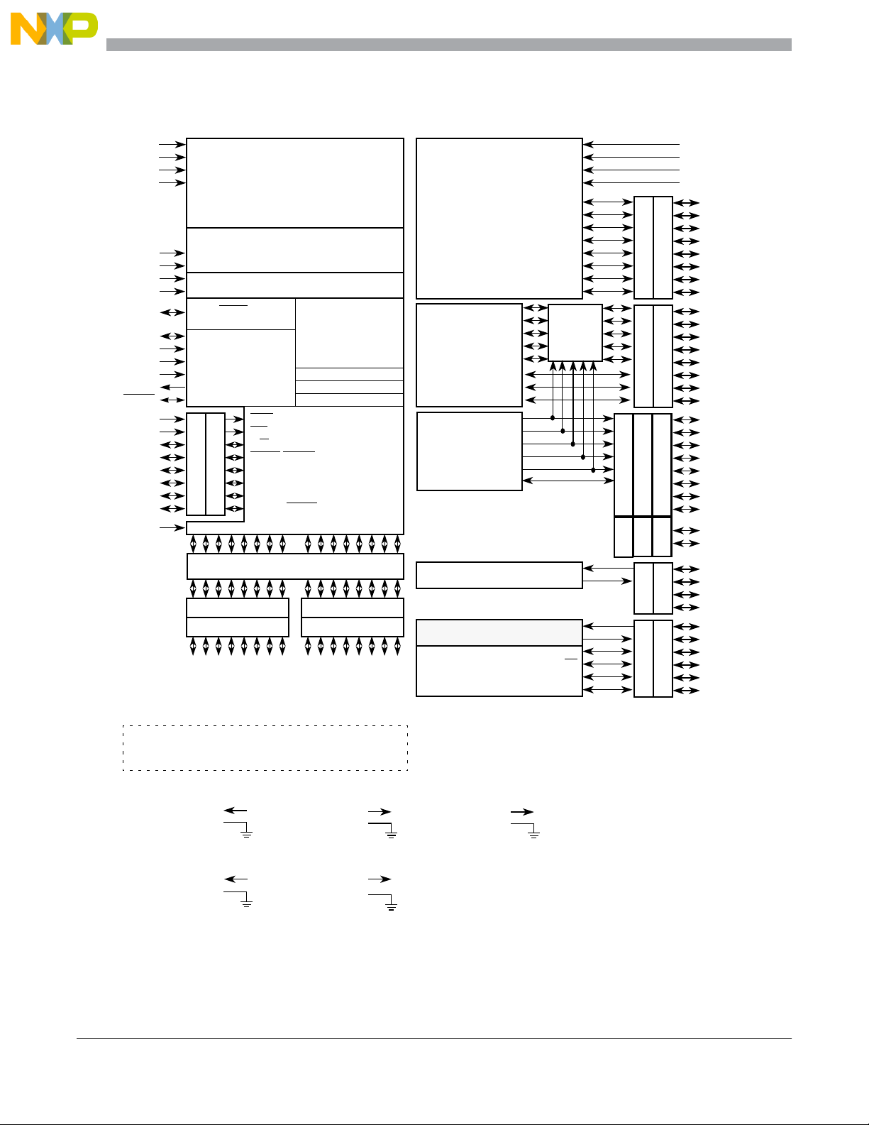
The MC9S12C-Family / MC9S12GC-Family are 48/52/80 pin Flash-based MCU families, which deliver
the power and flexibility of the 16-bit core to a whole new range of cost and space sensitive, general
purpose industrial and automotive network applications. All MC9S12C-Family / MC9S12GC-Family
members feature standard on-chip peripherals including a 16-bit central processing unit (CPU12), up to
128K bytes of Flash EEPROM, up to 4K bytes of RAM, an asynchronous serial communications interface
(SCI), a serial peripheral interface (SPI), an 8-channel 16-bit timer module (TIM), a 6-channel 8-bit pulse
width modulator (PWM), an 8-channel, 10-bit analog-to-digital converter (ADC).
The MC9S12C128-Family members also feature a CAN 2.0 A, B software compatible module
(MSCAN12).
All MC9S12C-Family / MC9S12GC-Family devices feature full 16-bit data paths throughout. The
inclusion of a PLL circuit allows power consumption and performance to be adjusted to suit operational
requirements. In addition to the I/O ports available in each module, up to 10 dedicated I/O port bits are
available with wake-up capability from stop or wait mode. The devices are available in 48-, 52-, and 80pin QFP packages, with the 80-pin version pin compatible to the HCS12 A, B, and D Family derivatives.
1.1.1 Features
• 16-bit HCS12 core:
— HCS12 CPU
– Upward compatible with M68HC11 instruction set
– Interrupt stacking and programmer’s model identical to M68HC11
– Instruction queue
– Enhanced indexed addressing
— MMC (memory map and interface)
— INT (interrupt control)
— BDM (background debug mode)
— DBG12 (enhanced debug12 module, including breakpoints and change-of-flow trace buffer)
— MEBI (multiplexed expansion bus interface) available only in 80-pin package version
• Wake-up interrupt inputs:
— Up to 12 port bits available for wake up interrupt function with digital filtering
Freescale Semiconductor MC9S12C-Family / MC9S12GC-Family 17
Rev 01.24

Chapter 1 MC9S12C and MC9S12GC Device Overview (MC9S12C128)
• Memory options:
— 16K or 32Kbyte Flash EEPROM (erasable in 512-byte sectors)
64K, 96K, or 128Kbyte Flash EEPROM (erasable in 1024-byte sectors)
— 1K, 2K or 4K Byte RAM
• Analog-to-digital converters:
— One 8-channel module with 10-bit resolution
— External conversion trigger capability
• Available on MC9S12C Family:
— One 1M bit per second, CAN 2.0 A, B software compatible module
— Five receive and three transmit buffers
— Flexible identifier filter programmable as 2 x 32 bit, 4 x 16 bit, or 8 x 8 bit
— Four separate interrupt channels for Rx, Tx, error, and wake-up
— Low-pass filter wake-up function
— Loop-back for self test operation
• Timer module (TIM):
— 8-channel timer
— Each channel configurable as either input capture or output compare
— Simple PWM mode
— Modulo reset of timer counter
— 16-bit pulse accumulator
— External event counting
— Gated time accumulation
• PWM module:
— Programmable period and duty cycle
— 8-bit 6-channel or 16-bit 3-channel
— Separate control for each pulse width and duty cycle
— Center-aligned or left-aligned outputs
— Programmable clock select logic with a wide range of frequencies
— Fast emergency shutdown input
• Serial interfaces:
— One asynchronous serial communications interface (SCI)
— One synchronous serial peripheral interface (SPI)
• CRG (clock reset generator module)
— Windowed COP watchdog
— Real time interrupt
— Clock monitor
— Pierce or low current Colpitts oscillator
— Phase-locked loop clock frequency multiplier
— Limp home mode in absence of external clock
— Low power 0.5MHz to 16MHz crystal oscillator reference clock
18 MC9S12C-Family / MC9S12GC-Family Freescale Semiconductor
Rev 01.24

Chapter 1 MC9S12C and MC9S12GC Device Overview (MC9S12C128)
• Operating frequency:
— 32MHz equivalent to 16MHz bus speed for single chip
— 32MHz equivalent to 16MHz bus speed in expanded bus modes
— Option of 9S12C Family: 50MHz equivalent to 25MHz bus speed
— All 9S12GC Family members allow a 50MHz operating frequency.
• Internal 2.5V regulator:
— Supports an input voltage range from 2.97V to 5.5V
— Low power mode capability
— Includes low voltage reset (LVR) circuitry
— Includes low voltage interrupt (LVI) circuitry
• 48-pin LQFP, 52-pin LQFP, or 80-pin QFP package:
— Up to 58 I/O lines with 5V input and drive capability (80-pin package)
— Up to 2 dedicated 5V input only lines (IRQ, XIRQ)
— 5V 8 A/D converter inputs and 5V I/O
• Development support:
— Single-wire background debug™ mode (BDM)
— On-chip hardware breakpoints
— Enhanced DBG12 debug features
1.1.2 Modes of Operation
User modes (expanded modes are only available in the 80-pin package version).
• Normal and emulation operating modes:
— Normal single-chip mode
— Normal expanded wide mode
— Normal expanded narrow mode
— Emulation expanded wide mode
— Emulation expanded narrow mode
• Special operating modes:
— Special single-chip mode with active background debug mode
— Special test mode (Freescale use only)
— Special peripheral mode (Freescale use only)
• Low power modes:
— Stop mode
— Pseudo stop mode
— Wait mode
Freescale Semiconductor MC9S12C-Family / MC9S12GC-Family 19
Rev 01.24
Chapter 1 MC9S12C and MC9S12GC Device Overview (MC9S12C128)
1.1.3 Block Diagram
V
V
V
BKGD
V
DDPLL
V
SSPLL
EXTAL
XTAL
RESET
TEST/V
V
V
V
V
V
XFC
PE0
PE1
PE2
PE3
PE4
PE5
PE6
PE7
SSR
DDR
DDX
SSX
DD2
SS2
DD1
SS1
V
DDA
V
SSA
V
RH
Voltage Regulator
V
RL
AN0
ATD
16K, 32K, 64K, 96K, 128K Byte Flash
AN1
AN2
AN3
AN4
AN5
AN6
AN7
MUX
MODC/TAGHI
PLL
PTE
DDRE
1K, 2K, 4K Byte RAM
BDM
Clock and
Reset
Generation
Module
XIRQ
IRQ
R/W
LSTRB/TAGLO
ECLK
MODA/IPIPE0
HCS12
CPU
COP Watchdog
Clock Monitor
Periodic Interrupt
System
Integration
Module
(SIM)
Timer
Module
PWM
Module
IOC0
IOC1
IOC2
IOC3
IOC4
IOC5
IOC6
IOC7
PW0
PW1
PW2
PW3
PW4
PW5
MODB/IPIPE1
NOACC/XCLKS
PP
Keypad Interrupt
Key Int
Multiplexed Address/Data Bus
DDRA DDRB
PTA PTB
SCI
MSCAN is not available on the
9S12GC Family Members
MSCAN
RXD
TXD
RXCAN
TXCAN
MISO
PA4
PA3
PA 2
PA 1
PA7
PA6
PA5
PA 0
PB7
PB6
PB5
PB4
PB3
PB2
PB1
PB0
SPI
SS
MOSI
SCK
DDRAD
DDRT
PTP
DDRP
PTJ
DDRJ
DDRS
DDRM
PTAD
PTT
PTS
PTM
V
DDA
V
SSA
V
RH
V
RL
PAD0
PAD1
PAD2
PAD3
PAD4
PAD5
PAD6
PAD7
PT0
PT1
PT2
PT3
PT4
PT5
PT6
PT7
PP0
PP1
PP2
PP3
PP4
PP5
PP6
PP7
PJ6
PJ7
PS0
PS1
PS2
PS3
PM0
PM1
PM2
PM3
PM4
PM5
ADDR12
ADDR11
ADDR10
ADDR9
ADDR8
DATA11
DATA1 0
DATA9
DATA8
ADDR7
ADDR6
ADDR5
DATA4
DATA7
DATA6
DATA5
I/O Driver 5V
V
DDX
V
SSX
ADDR4
ADDR3
DATA3
ADDR2
ADDR1
DATA2
DATA1
ADDR0
Signals shown in Bold are not available on the 52 or 48 Pin Package
DATA0
Signals shown in Bold Italic are available in the 52, but not the 48 Pin Package
Voltage Regulator 5V & I/O
V
DDR
V
SSR
A/D Converter 5V
V
DDA
V
SSA
VRL is bonded internally to V
for 52- and 48-Pin packages
SSA
Multiplexed
Wide Bus
ADDR15
ADDR14
ADDR13
DATA12
DATA15
DATA14
DATA13
Internal Logic 2.5V
V
DD1,2
V
SS1,2
PLL 2.5V
V
DDPLL
V
SSPLL
Figure 1-1. MC9S12C-Family / MC9S12GC-Family Block Diagram
20 MC9S12C-Family / MC9S12GC-Family Freescale Semiconductor
Rev 01.24
Chapter 1 MC9S12C and MC9S12GC Device Overview (MC9S12C128)
1.2 Memory Map and Registers
1.2.1 Device Memory Map
Table 1-1 shows the device register map after reset. Figure 1-2 through Figure 1-6 illustrate the full device
memory map.
Table 1-1. Device Register Map Overview
Address Module Size
0x0000–0x0017 Core (ports A, B, E, modes, inits, test) 24
0x0018 Reserved 1
0x0019 Voltage regulator (VREG) 1
0x001A–0x001B Device ID register 2
0x001C–0x001F Core (MEMSIZ, IRQ, HPRIO) 4
0x0020–0x002F Core (DBG) 16
0x0030–0x0033 Core (PPAGE
0x0034–0x003F Clock and reset generator (CRG) 12
0x0040–0x006F Standard timer module (TIM) 48
0x0070–0x007F Reserved 16
0x0080–0x009F Analog-to-digital converter (ATD) 32
0x00A0–0x00C7 Reserved 40
0x00C8–0x00CF Serial communications interface (SCI) 8
0x00D0–0x00D7 Reserved 8
0x00D8–0x00DF Serial peripheral interface (SPI) 8
0x00E0–0x00FF Pulse width modulator (PWM) 32
0x0100–0x010F Flash control register 16
0x0110–0x013F Reserved 48
0x0140–0x017F Scalable controller area network (MSCAN)
0x0180–0x023F Reserved 192
0x0240–0x027F Port integration module (PIM) 64
0x0280–0x03FF Reserved 384
1. External memory paging is not supported on this device (Section 1.7.1, “PPAGE”).
2. Not available on MC9S12GC Family devices
(1)
)
(2)
4
64
Freescale Semiconductor MC9S12C-Family / MC9S12GC-Family 21
Rev 01.24

Chapter 1 MC9S12C and MC9S12GC Device Overview (MC9S12C128)
0x0000
0x0400
0x3000
0x4000
0x8000
EXT
0xC000
0xFF00
0xFFFF
The figure shows a useful map, which is not the map out of reset. After reset the map is:
0x0000–0x03FF: Register Space
0x0000–0x0FFF: 4K RAM (only 3K visible 0x0400–0x0FFF)
Flash erase sector size is 1024 bytes
VECTORS
NORMAL
SINGLE CHIP
VECTORS
EXPANDED SPECIAL
VECTORS
SINGLE CHIP
Figure 1-2. MC9S12C128 and MC9S12GC128 User Configurable Memory Map
0x0000
0x03FF
0x0000
0x3FFF
0x3000
0x3FFF
0x4000
0x7FFF
0x8000
0xBFFF
0xC000
0xFFFF
0xFF00
0xFFFF
1K Register Space
Mappable to any 2K Boundary
16K Fixed Flash EEPROM
4K Bytes RAM
Mappable to any 4K Boundary
16K Fixed Flash EEPROM
16K Page Window
8 * 16K Flash EEPROM Pages
16K Fixed Flash EEPROM
BDM
(If Active)
PAGE MAP
0x003D
0x003E
PPAGE
0x003F
22 MC9S12C-Family / MC9S12GC-Family Freescale Semiconductor
Rev 01.24

Chapter 1 MC9S12C and MC9S12GC Device Overview (MC9S12C128)
0x0000
0x0400
0x3000
0x4000
0x8000
EXT
0xC000
0xFF00
0xFFFF
The figure shows a useful map, which is not the map out of reset. After reset the map is:
Flash erase sector size is 1024 bytes
VECTORS
NORMAL
SINGLE CHIP
0x0000–0x03FF: Register Space
0x0000–0x0FFF: 4K RAM (only 3K visible 0x0400–0x0FFF)
VECTORS
EXPANDED SPECIAL
VECTORS
SINGLE CHIP
0x0000
0x03FF
0x0000
0x3FFF
0x3000
0x3FFF
0x4000
0x7FFF
0x8000
0xBFFF
0xC000
0xFFFF
0xFF00
0xFFFF
1K Register Space
Mappable to any 2K Boundary
16K Fixed Flash EEPROM
4K Bytes RAM
Mappable to any 4K Boundary
16K Fixed Flash EEPROM
16K Page Window
6 * 16K Flash EEPROM Pages
16K Fixed Flash EEPROM
BDM
(If Active)
PAGE MAP
0x003D
0x003E
PPAGE
0x003F
Figure 1-3. MC9S12C96 and MC9S12GC96 User Configurable Memory Map
Freescale Semiconductor MC9S12C-Family / MC9S12GC-Family 23
Rev 01.24
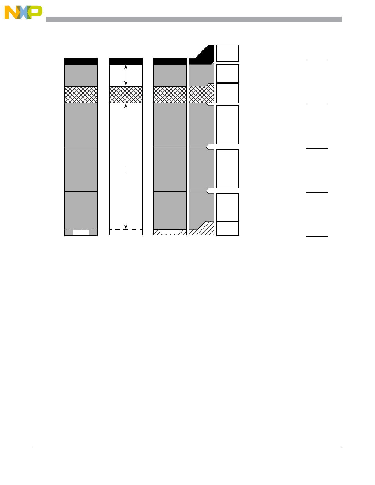
Chapter 1 MC9S12C and MC9S12GC Device Overview (MC9S12C128)
0x0000
0x0400
0x3000
0x4000
0x8000
EXT
0xC000
0xFF00
0xFFFF
The figure shows a useful map, which is not the map out of reset. After reset the map is:
Flash erase sector size is 1024 Bytes
VECTORS
NORMAL
SINGLE CHIP
0x0000–0x03FF: Register space
0x0000–0x0FFF: 4K RAM (only 3K visible 0x0400–0x0FFF)
VECTORS
EXPANDED SPECIAL
VECTORS
SINGLE CHIP
0x0000
0x03FF
0x0000
0x3FFF
0x3000
0x3FFF
0x4000
0x7FFF
0x8000
0xBFFF
0xC000
0xFFFF
0xFF00
0xFFFF
1K Register Space
Mappable to any 2K Boundary
16K Fixed Flash EEPROM
4K Bytes RAM
Mappable to any 4K Boundary
16K Fixed Flash EEPROM
16K Page Window
4 * 16K Flash EEPROM Pages
16K Fixed Flash EEPROM
BDM
(If Active)
PAGE MAP
0x003D
0x003E
PPAGE
0x003F
Figure 1-4. MC9S12C64 and MC9S12GC64 User Configurable Memory Map
24 MC9S12C-Family / MC9S12GC-Family Freescale Semiconductor
Rev 01.24
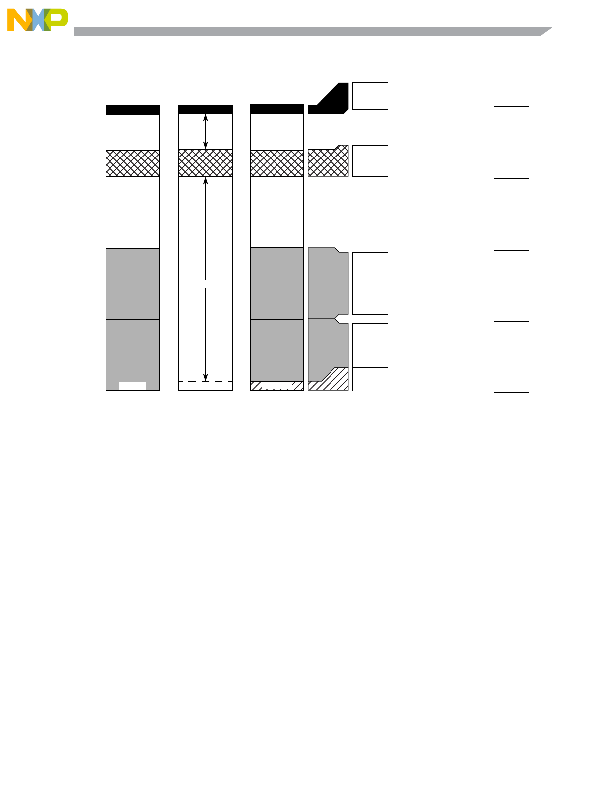
Chapter 1 MC9S12C and MC9S12GC Device Overview (MC9S12C128)
0x0000
0x0400
0x3800
0x4000
0x8000
0xC000
0xFF00
0xFFFF
VECTORS
NORMAL
SINGLE CHIP
EXT
VECTORS
EXPANDED SPECIAL
VECTORS
SINGLE CHIP
0x0000
0x03FF
0x3800
0x3FFF
0x8000
0xBFFF
0xC000
0xFFFF
0xFF00
0xFFFF
1K Register Space
Mappable to any 2K Boundary
2K Bytes RAM
Mappable to any 2K Boundary
16K Page Window
2 * 16K Flash EEPROM Pages
16K Fixed Flash EEPROM
BDM
(If Active)
PAGE MAP
0x003E
PPAGE
0x003F
The figure shows a useful map, which is not the map out of reset. After reset the map is:
0x0000–0x03FF: Register space
0x0800–0x0FFF: 2K RAM
Flash erase sector size is 512 bytes
The flash page 0x003E is visible at 0x4000–0x7FFF in the memory map if ROMHM = 0.
In the figure ROMHM = 1 removing page 0x003E from 0x4000–0x7FFF.
Figure 1-5. MC9S12C32 and MC9S12GC32 User Configurable Memory Map
Freescale Semiconductor MC9S12C-Family / MC9S12GC-Family 25
Rev 01.24

Chapter 1 MC9S12C and MC9S12GC Device Overview (MC9S12C128)
0x0000
0x0400
0x3C00
0x4000
0x8000
EXT
0xC000
0xFF00
0xFFFF
The figure shows a useful map, which is not the map out of reset. After reset the map is:
VECTORS
NORMAL
SINGLE CHIP
0x0000–0x03FF: Register Space
0x0C00–0x0FFF: 1K RAM
VECTORS
EXPANDED SPECIAL
VECTORS
SINGLE CHIP
0x0000
0x03FF
0x3C00
0x3FFF
0x8000
0xBFFF
0xC000
0xFFFF
0xFF00
0xFFFF
1K Register Space
Mappable to any 2K Boundary
1K Bytes RAM
Mappable to any 2K Boundary
16K Page Window
16K Fixed Flash EEPROM
BDM
(If Active)
PAGE MAP
PPAGE
0x003F
The 16K flash array page 0x003F is also visible in the PPAGE window when PPAGE register contents are odd.
Flash Erase Sector Size is 512 Bytes
Figure 1-6. MC9S12GC16 User Configurable Memory Map
26 MC9S12C-Family / MC9S12GC-Family Freescale Semiconductor
Rev 01.24

Chapter 1 MC9S12C and MC9S12GC Device Overview (MC9S12C128)
1.2.2 Detailed Register Map
The detailed register map of the MC9S12C128
is listed in address order below.
0x0000–0x000F MEBI Map 1 of 3 (HCS12 Multiplexed External Bus Interface)
Address Name Bit 7 Bit 6 Bit 5 Bit 4 Bit 3 Bit 2 Bit 1 Bit 0
0x0000 PORTA
0x0001 PORTB
0x0002 DDRA
0x0003 DDRB
0x0004 Reserved
0x0005 Reserved
0x0006 Reserved
0x0007 Reserved
0x0008 PORTE
0x0009 DDRE
0x000A PEAR
0x000B MODE
0x000C PUCR
0x000D RDRIV
0x000E EBICTL
0x000F Reserved
Read:
Write:
Read:
Write:
Read:
Write:
Read:
Write:
Read: 0 0 0 0 0 0 0 0
Write:
Read: 0 0 0 0 0 0 0 0
Write:
Read: 0 0 0 0 0 0 0 0
Write:
Read: 0 0 0 0 0 0 0 0
Write:
Read:
Write:
Read:
Write:
Read:
Write:
Read:
Write:
Read:
Write:
Read:
Write:
Read: 0 0 0 0 0 0 0
Write:
Read: 0 0 0 0 0 0 0 0
Write:
Bit 7 6 5 4 3 2 1 Bit 0
Bit 7 6 5 4 3 2 1 Bit 0
Bit 7 6 5 4 3 2 1 Bit 0
Bit 7 6 5 4 3 2 1 Bit 0
Bit 7 6 5 4 3 2
Bit 7 6 5 4 3 Bit 2
NOACCE
MODC MODB MODA
PUPKE
RDPK
0
00
00
PIPOE NECLK LSTRE RDWE
PUPEE
RDPE
0
IVIS
00
00
0
Bit 1 Bit 0
00
00
EMK EME
PUPBE PUPAE
RDPB RDPA
ESTR
Freescale Semiconductor MC9S12C-Family / MC9S12GC-Family 27
Rev 01.24
Chapter 1 MC9S12C and MC9S12GC Device Overview (MC9S12C128)
0x0010–0x0014 MMC Map 1 of 4 (HCS12 Module Mapping Control)
Address Name Bit 7 Bit 6 Bit 5 Bit 4 Bit 3 Bit 2 Bit 1 Bit 0
0x0010 INITRM
0x0011 INITRG
0x0012 INITEE
0x0013 MISC
0x0014 Reserved
Read:
Write:
Read: 0
Write:
Read:
Write:
Read: 0 0 0 0
Write:
Read: 0 0 0 0 0 0 0 0
Write:
RAM15 RAM14 RAM13 RAM12 RAM11
REG14 REG13 REG12 REG11
EE15 EE14 EE13 EE12 EE11
EXSTR1 EXSTR0 ROMHM ROMON
00
000
00
RAMHAL
EEON
0x0015–0x0016 INT Map 1 of 2 (HCS12 Interrupt)
Address Name Bit 7 Bit 6 Bit 5 Bit 4 Bit 3 Bit 2 Bit 1 Bit 0
0x0015 ITCR
0x0016 ITEST
Read: 0 0 0
Write:
Read:
Write:
INTE INTC INTA INT8 INT6 INT4 INT2 INT0
WRINT ADR3 ADR2 ADR1 ADR0
0x0017–0x0017 MMC Map 2 of 4 (HCS12 Module Mapping Control)
Address Name Bit 7 Bit 6 Bit 5 Bit 4 Bit 3 Bit 2 Bit 1 Bit 0
0x0017 Reserved
Read: 0 0 0 0 0 0 0 0
Write:
0x0018–0x0018 Miscellaneous Peripherals (Device User Guide)
Address Name Bit 7 Bit 6 Bit 5 Bit 4 Bit 3 Bit 2 Bit 1 Bit 0
0x0018 Reserved
Read: 0 0 0 0 0 0 0 0
Write:
0x0019–0x0019 VREG3V3 (Voltage Regulator)
Address Name Bit 7 Bit 6 Bit 5 Bit 4 Bit 3 Bit 2 Bit 1 Bit 0
$0019 VREGCTRL
Read: 0 0 0 0 0 LVDS
Write:
LVIE LVIF
28 MC9S12C-Family / MC9S12GC-Family Freescale Semiconductor
Rev 01.24
Chapter 1 MC9S12C and MC9S12GC Device Overview (MC9S12C128)
0x001A–0x001B Miscellaneous Peripherals (Device User Guide)
Address Name Bit 7 Bit 6 Bit 5 Bit 4 Bit 3 Bit 2 Bit 1 Bit 0
0x001A PARTIDH
0x001B PARTIDL
Read: ID15 ID14 ID13 ID12 ID11 ID10 ID9 ID8
Write:
Read: ID7 ID6 ID5 ID4 ID3 ID2 ID1 ID0
Write:
0x001C–0x001D MMC Map 3 of 4 (HCS12 Module Mapping Control, Device User Guide)
Address Name Bit 7 Bit 6 Bit 5 Bit 4 Bit 3 Bit 2 Bit 1 Bit 0
0x001C MEMSIZ0
0x001D MEMSIZ1
Read:
Write:
Read:
Write:
reg_sw0 0 eep_sw1 eep_sw0 0 ram_sw2 ram_sw1 ram_sw0
rom_sw1 rom_sw0 0 0 0 0 pag_sw1 pag_sw0
0x001E–0x001E MEBI Map 2 of 3 (HCS12 Multiplexed External Bus Interface)
Address Name Bit 7 Bit 6 Bit 5 Bit 4 Bit 3 Bit 2 Bit 1 Bit 0
0x001E INTCR
Read:
Write:
IRQE IRQEN
000000
0x001F–0x001F INT Map 2 of 2 (HCS12 Interrupt)
Address Name Bit 7 Bit 6 Bit 5 Bit 4 Bit 3 Bit 2 Bit 1 Bit 0
0x001F HPRIO
Read:
Write:
PSEL7 PSEL6 PSEL5 PSEL4 PSEL3 PSEL2 PSEL1
0x0020–0x002F DBG (Including BKP) Map 1 of 1 (HCS12 Debug)
Address Name Bit 7 Bit 6 Bit 5 Bit 4 Bit 3 Bit 2 Bit 1 Bit 0
0x0020 DBGC1
0x0021 DBGSC
0x0022 DBGTBH
0x0023 DBGTBL
0x0024 DBGCNT
0x0025 DBGCCX
Read:
Write:
Read: AF BF CF 0
Write:
Read: Bit 15 Bit 14 Bit 13 Bit 12 Bit 11 Bit 10 Bit 9 Bit 8
Write:
Read: Bit 7 Bit 6 Bit 5 Bit 4 Bit 3 Bit 2 Bit 1 Bit 0
Write:
Read: TBF 0 CNT
Write:
Read:
Write:
DBGEN ARM TRGSEL BEGIN DBGBRK
PAGSEL EXTCMP
0
TRG
CAPMOD
0
Freescale Semiconductor MC9S12C-Family / MC9S12GC-Family 29
Rev 01.24
Chapter 1 MC9S12C and MC9S12GC Device Overview (MC9S12C128)
0x0020–0x002F DBG (Including BKP) Map 1 of 1 (HCS12 Debug) (continued)
Address Name Bit 7 Bit 6 Bit 5 Bit 4 Bit 3 Bit 2 Bit 1 Bit 0
0x0026 DBGCCH
0x0027 DBGCCL
0x0028
0x0029
0x002A
0x002B
0x002C
0x002D
0x002E
0x002F
DBGC2 Read:
BKPCT0 Write:
DBGC3 Read:
BKPCT1 Write:
DBGCAX Read:
BKP0X Write:
DBGCAH Read:
BKP0H Write:
DBGCAL Read:
BKP0L Write:
DBGCBX Read:
BKP1X Write:
DBGCBH Read:
BKP1H Write:
DBGCBL Read:
BKP1L Write:
Read:
Write:
Read:
Write:
Bit 15 14 13 12 11 10 9 Bit 8
Bit 7 6 5 4 3 2 1 Bit 0
BKABEN FULL BDM TAGAB BKCEN TAGC RWCEN RWC
BKAMBH BKAMBL BKBMBH BKBMBL RWAEN RWA RWBEN RWB
PAGSEL EXTCMP
Bit 15 14 13 12 11 10 9 Bit 8
Bit 7 6 5 4 3 2 1 Bit 0
PAGSEL EXTCMP
Bit 15 14 13 12 11 10 9 Bit 8
Bit 7 6 5 4 3 2 1 Bit 0
0x0030–0x0031 MMC Map 4 of 4 (HCS12 Module Mapping Control)
Address Name Bit 7 Bit 6 Bit 5 Bit 4 Bit 3 Bit 2 Bit 1 Bit 0
0x0030 PPAGE
0x0031 Reserved
Read: 0 0
Write:
Read: 0 0 0 0 0 0 0 0
Write:
PIX5 PIX4 PIX3 PIX2 PIX1 PIX0
0x0032–0x0033 MEBI Map 3 of 3 (HCS12 Multiplexed External Bus Interface)
Address Name Bit 7 Bit 6 Bit 5 Bit 4 Bit 3 Bit 2 Bit 1 Bit 0
Read:
0x0032 PORTK
0x0033 DDRK
(1)
1
Write:
Read:
Write:
Address Name Bit 7 Bit 6 Bit 5 Bit 4 Bit 3 Bit 2 Bit 1 Bit 0
$0032 Reserved
$0033 Reserved
1. Only applicable in special emulation-only bond outs, for emulation of extended memory map.
Read: 0 0 0 0 0 0 0 0
Write:
Read: 0 0 0 0 0 0 0 0
Write:
Bit 7 6 5 4 3 2 1 Bit 0
Bit 7 6 5 4 3 2 1 Bit 0
30 MC9S12C-Family / MC9S12GC-Family Freescale Semiconductor
Rev 01.24
 Loading...