

Page 1

MC68HC08KH12
Data Sheet
M68HC08
Microcontrollers
Rev. 1.1
MC68HC08KH12/H
July 15, 2005
freescale.com
Page 2

Page 3

Advance Information — MC68HC(7)08KH12
Section 1. General Description .......................................23
Section 2. Memory Map ...................................................33
Section 3. Random-Access Memory (RAM) ...................45
Section 4. Read-Only Memory (ROM) .............................47
Section 5. Configuration Register (CONFIG) .................49
Section 6. Central Processor Unit (CPU) .......................51
Section 7. System Integration Module (SIM) .................61
List of Sections
Section 8. Clock Generator Module (CGM) ....................87
Section 9. Universal Serial Bus Module (USB) ............113
Section 10. Monitor ROM (MON) ...................................149
Section 11. Timer Interface Module (TIM) ....................161
Section 12. I/O Ports ......................................................183
Section 13. Computer Operating Properly (COP) .......207
Section 14. External Interrupt (IRQ) .............................213
Section 15. Keyboard Interrupt Module (KBI) ..............219
Section 16. Break Module (BREAK) .............................241
Section 17. Preliminary Electrical Specifications .......247
Section 18. Mechanical Specifications ........................259
MC68HC(7)08KH12 — Rev. 1.1 Advance Information
Freescale Semiconductor
3
Page 4

Advance Information MC68HC(7)08KH12 — Rev. 1.1
4 Freescale Semiconductor
Page 5

Advance Information — MC68HC(7)08KH12
General Description
1.1 Contents . . . . . . . . . . . . . . . . . . . . . . . . . . . . . . . . . . . . . . . . . .23
1.2 Introduction. . . . . . . . . . . . . . . . . . . . . . . . . . . . . . . . . . . . . . . .24
1.3 Features . . . . . . . . . . . . . . . . . . . . . . . . . . . . . . . . . . . . . . . . . .24
1.4 MCU Block Diagram. . . . . . . . . . . . . . . . . . . . . . . . . . . . . . . . .26
1.5 Pin Assignments. . . . . . . . . . . . . . . . . . . . . . . . . . . . . . . . . . . .28
1.5.1 Quad Flat Pack (QFP) Package . . . . . . . . . . . . . . . . . . . . .28
1.5.2 Power Supply Pins
(V
1.5.3 Oscillator Pins (OSC1 and OSC2) . . . . . . . . . . . . . . . . . . .30
1.5.4 External Reset Pin (RST) . . . . . . . . . . . . . . . . . . . . . . . . . .30
1.5.5 External Interrupt Pin (IRQ1/VPP) . . . . . . . . . . . . . . . . . . . .30
1.5.6 USB Data Pins
(DPLUS0–DPLUS4 and DMINUS0–DMINUS4). . . . . . .30
1.5.7 Voltage Regulator Out (REGOUT) . . . . . . . . . . . . . . . . . . .30
1.5.8 Port A Input/Output (I/O) Pins (PTA7–PTA0) . . . . . . . . . . .31
1.5.9 Port B I/O Pins (PTB7–PTB0). . . . . . . . . . . . . . . . . . . . . . .31
1.5.10 Port C I/O Pins (PTC4–PTC0). . . . . . . . . . . . . . . . . . . . . . .31
1.5.11 Port D I/O Pins (PTD7/KBD7–PTD0/KBD0) . . . . . . . . . . . .31
1.5.12 Port E I/O Pins (PTE4, PTE3/KBE3, PTE2/KBE2/TCH1,
PTE1/KBE1/TCH0, PTE0/KBE0/TCLK). . . . . . . . . . . . .31
1.5.13 Port F I/O Pins (PTF7/KBF7–PTF0/KBF0) . . . . . . . . . . . . .32
DDA
, V
SSA
, V
DD1
, V
SS1
Table of Contents
, V
DD2
, and V
) . . . . . . . . . .29
SS2
Section 2. Memory Map
2.1 Contents . . . . . . . . . . . . . . . . . . . . . . . . . . . . . . . . . . . . . . . . . .33
2.2 Introduction. . . . . . . . . . . . . . . . . . . . . . . . . . . . . . . . . . . . . . . .33
MC68HC(7)08KH12 — Rev. 1.1 Advance Information
Freescale Semiconductor
5
Page 6

2.3 I/O Section . . . . . . . . . . . . . . . . . . . . . . . . . . . . . . . . . . . . . . . .35
2.4 Monitor ROM . . . . . . . . . . . . . . . . . . . . . . . . . . . . . . . . . . . . . .43
Section 3. Random-Access Memory (RAM)
3.1 Contents . . . . . . . . . . . . . . . . . . . . . . . . . . . . . . . . . . . . . . . . . .45
3.2 Introduction. . . . . . . . . . . . . . . . . . . . . . . . . . . . . . . . . . . . . . . .45
3.3 Functional Description . . . . . . . . . . . . . . . . . . . . . . . . . . . . . . .45
Section 4. Read-Only Memory (ROM)
4.1 Contents . . . . . . . . . . . . . . . . . . . . . . . . . . . . . . . . . . . . . . . . . .47
4.2 Introduction. . . . . . . . . . . . . . . . . . . . . . . . . . . . . . . . . . . . . . . .47
4.3 Functional Description . . . . . . . . . . . . . . . . . . . . . . . . . . . . . . .47
5.1 Contents . . . . . . . . . . . . . . . . . . . . . . . . . . . . . . . . . . . . . . . . . .49
5.2 Introduction. . . . . . . . . . . . . . . . . . . . . . . . . . . . . . . . . . . . . . . .49
5.3 Functional Description . . . . . . . . . . . . . . . . . . . . . . . . . . . . . . .49
Section 5. Configuration Register (CONFIG)
Section 6. Central Processor Unit (CPU)
6.1 Contents . . . . . . . . . . . . . . . . . . . . . . . . . . . . . . . . . . . . . . . . . .51
6.2 Introduction. . . . . . . . . . . . . . . . . . . . . . . . . . . . . . . . . . . . . . . .51
6.3 Features . . . . . . . . . . . . . . . . . . . . . . . . . . . . . . . . . . . . . . . . . .52
6.4 CPU Registers . . . . . . . . . . . . . . . . . . . . . . . . . . . . . . . . . . . . .52
6.4.1 Accumulator (A). . . . . . . . . . . . . . . . . . . . . . . . . . . . . . . . . .53
6.4.2 Index Register (H:X) . . . . . . . . . . . . . . . . . . . . . . . . . . . . . .54
6.4.3 Stack Pointer (SP). . . . . . . . . . . . . . . . . . . . . . . . . . . . . . . .55
6.4.4 Program Counter (PC) . . . . . . . . . . . . . . . . . . . . . . . . . . . .56
6.4.5 Condition Code Register (CCR) . . . . . . . . . . . . . . . . . . . . .57
6.5 Arithmetic/Logic Unit (ALU) . . . . . . . . . . . . . . . . . . . . . . . . . . .59
Advance Information MC68HC(7)08KH12 — Rev. 1.1
6 Freescale Semiconductor
Page 7

Section 7. System Integration Module (SIM)
7.1 Contents . . . . . . . . . . . . . . . . . . . . . . . . . . . . . . . . . . . . . . . . . .61
7.2 Introduction. . . . . . . . . . . . . . . . . . . . . . . . . . . . . . . . . . . . . . . .62
7.3 SIM Bus Clock Control and Generation . . . . . . . . . . . . . . . . . .65
7.3.1 Bus Timing . . . . . . . . . . . . . . . . . . . . . . . . . . . . . . . . . . . . .65
7.3.2 Clock Start-Up from POR . . . . . . . . . . . . . . . . . . . . . . . . . .66
7.3.3 Clocks in Stop Mode and Wait Mode . . . . . . . . . . . . . . . . .66
7.4 Reset and System Initialization. . . . . . . . . . . . . . . . . . . . . . . . .66
7.4.1 External Pin Reset. . . . . . . . . . . . . . . . . . . . . . . . . . . . . . . .67
7.4.2 Active Resets from Internal Sources. . . . . . . . . . . . . . . . . .67
7.4.2.1 Power-On Reset . . . . . . . . . . . . . . . . . . . . . . . . . . . . . . .68
7.4.2.2 Computer Operating Properly (COP) Reset. . . . . . . . . . .69
7.4.2.3 Illegal Opcode Reset . . . . . . . . . . . . . . . . . . . . . . . . . . . .70
7.4.2.4 Illegal Address Reset. . . . . . . . . . . . . . . . . . . . . . . . . . . .70
7.4.2.5 Universal Serial Bus Reset . . . . . . . . . . . . . . . . . . . . . . .70
7.5 SIM Counter . . . . . . . . . . . . . . . . . . . . . . . . . . . . . . . . . . . . . . .71
7.5.1 SIM Counter During Power-On Reset. . . . . . . . . . . . . . . . .71
7.5.2 SIM Counter During Stop Mode Recovery . . . . . . . . . . . . .71
7.5.3 SIM Counter and Reset States . . . . . . . . . . . . . . . . . . . . . .71
7.6 Exception Control . . . . . . . . . . . . . . . . . . . . . . . . . . . . . . . . . . .72
7.6.1 Interrupts. . . . . . . . . . . . . . . . . . . . . . . . . . . . . . . . . . . . . . .72
7.6.1.1 Hardware Interrupts . . . . . . . . . . . . . . . . . . . . . . . . . . . . .74
7.6.1.2 SWI Instruction. . . . . . . . . . . . . . . . . . . . . . . . . . . . . . . . .76
7.6.2 Interrupt Status Registers . . . . . . . . . . . . . . . . . . . . . . . . . .76
7.6.2.1 Interrupt Status Register 1. . . . . . . . . . . . . . . . . . . . . . . .77
7.6.2.2 Interrupt Status Register 2. . . . . . . . . . . . . . . . . . . . . . . .78
7.6.2.3 Interrupt Status Register 3. . . . . . . . . . . . . . . . . . . . . . . .78
7.6.3 Reset. . . . . . . . . . . . . . . . . . . . . . . . . . . . . . . . . . . . . . . . . .79
7.6.4 Break Interrupts. . . . . . . . . . . . . . . . . . . . . . . . . . . . . . . . . .79
7.6.5 Status Flag Protection in Break Mode. . . . . . . . . . . . . . . . .79
7.7 Low-Power Modes . . . . . . . . . . . . . . . . . . . . . . . . . . . . . . . . . .79
7.7.1 Wait Mode. . . . . . . . . . . . . . . . . . . . . . . . . . . . . . . . . . . . . .80
7.7.2 Stop Mode. . . . . . . . . . . . . . . . . . . . . . . . . . . . . . . . . . . . . .81
7.8 SIM Registers. . . . . . . . . . . . . . . . . . . . . . . . . . . . . . . . . . . . . .83
7.8.1 Break Status Register (BSR). . . . . . . . . . . . . . . . . . . . . . . .83
MC68HC(7)08KH12 — Rev. 1.1 Advance Information
Freescale Semiconductor
7
Page 8

7.8.2 Reset Status Register (RSR) . . . . . . . . . . . . . . . . . . . . . . .84
7.8.3 Break Flag Control Register (BFCR). . . . . . . . . . . . . . . . . .85
Section 8. Clock Generator Module (CGM)
8.1 Contents . . . . . . . . . . . . . . . . . . . . . . . . . . . . . . . . . . . . . . . . . .87
8.2 Introduction. . . . . . . . . . . . . . . . . . . . . . . . . . . . . . . . . . . . . . . .88
8.3 Features . . . . . . . . . . . . . . . . . . . . . . . . . . . . . . . . . . . . . . . . . .89
8.4 Functional Description . . . . . . . . . . . . . . . . . . . . . . . . . . . . . . .89
8.4.1 Crystal Oscillator Circuit . . . . . . . . . . . . . . . . . . . . . . . . . . .91
8.4.2 Phase-Locked Loop Circuit (PLL) . . . . . . . . . . . . . . . . . . . .91
8.4.3 PLL Circuits. . . . . . . . . . . . . . . . . . . . . . . . . . . . . . . . . . . . .91
8.4.4 Acquisition and Tracking Modes . . . . . . . . . . . . . . . . . . . . .93
8.4.5 Manual and Automatic PLL Bandwidth Modes . . . . . . . . . .93
8.4.6 Programming the PLL . . . . . . . . . . . . . . . . . . . . . . . . . . . . .94
8.4.7 Special Programming Exceptions . . . . . . . . . . . . . . . . . . . .95
8.4.8 Base Clock Selector Circuit. . . . . . . . . . . . . . . . . . . . . . . . .96
8.4.9 CGM External Connections. . . . . . . . . . . . . . . . . . . . . . . . .96
8.5 I/O Signals . . . . . . . . . . . . . . . . . . . . . . . . . . . . . . . . . . . . . . . .98
8.5.1 Crystal Amplifier Input Pin (OSC1) . . . . . . . . . . . . . . . . . . .98
8.5.2 Crystal Amplifier Output Pin (OSC2). . . . . . . . . . . . . . . . . .98
8.5.3 External Filter Capacitor Pin (CGMXFC). . . . . . . . . . . . . . .98
8.5.4 PLL Analog Power Pin (V
8.5.5 PLL Analog Ground Pin (V
) . . . . . . . . . . . . . . . . . . . . . .98
DDA
). . . . . . . . . . . . . . . . . . . . . .98
SSA
8.5.6 Buffered Crystal Clock Output (CGMVOUT). . . . . . . . . . . .99
8.5.7 CGMVSEL. . . . . . . . . . . . . . . . . . . . . . . . . . . . . . . . . . . . . .99
8.5.8 Oscillator Enable Signal (SIMOSCEN) . . . . . . . . . . . . . . . .99
8.5.9 Crystal Output Frequency Signal (CGMXCLK). . . . . . . . . .99
8.5.10 CGM Base Clock Output (CGMOUT) . . . . . . . . . . . . . . . . .99
8.5.11 CGM CPU Interrupt (CGMINT) . . . . . . . . . . . . . . . . . . . . . .99
8.6 CGM Registers. . . . . . . . . . . . . . . . . . . . . . . . . . . . . . . . . . . .100
8.6.1 PLL Control Register (PCTL) . . . . . . . . . . . . . . . . . . . . . .102
8.6.2 PLL Bandwidth Control Register (PBWC). . . . . . . . . . . . .104
8.6.3 PLL Multiplier Select Registers (PMSH:PMSL). . . . . . . . .105
8.6.4 PLL Reference Divider Select Register (PRDS) . . . . . . . .106
Advance Information MC68HC(7)08KH12 — Rev. 1.1
8 Freescale Semiconductor
Page 9

8.7 Interrupts. . . . . . . . . . . . . . . . . . . . . . . . . . . . . . . . . . . . . . . . .107
8.8 Special Modes . . . . . . . . . . . . . . . . . . . . . . . . . . . . . . . . . . . .107
8.8.1 Wait Mode. . . . . . . . . . . . . . . . . . . . . . . . . . . . . . . . . . . . .107
8.8.2 CGM During Break Interrupts . . . . . . . . . . . . . . . . . . . . . .108
8.9 Acquisition/Lock Time Specifications . . . . . . . . . . . . . . . . . . .108
8.9.1 Acquisition/Lock Time Definitions . . . . . . . . . . . . . . . . . . .108
8.9.2 Parametric Influences on Reaction Time . . . . . . . . . . . . .109
8.9.3 Choosing a Filter Capacitor. . . . . . . . . . . . . . . . . . . . . . . .111
8.9.4 Reaction Time Calculation . . . . . . . . . . . . . . . . . . . . . . . .111
Section 9. Universal Serial Bus Module (USB)
9.1 Contents . . . . . . . . . . . . . . . . . . . . . . . . . . . . . . . . . . . . . . . . .113
9.2 Features . . . . . . . . . . . . . . . . . . . . . . . . . . . . . . . . . . . . . . . . .114
9.3 Overview. . . . . . . . . . . . . . . . . . . . . . . . . . . . . . . . . . . . . . . . .115
9.4 I/O Register Description of the HUB function . . . . . . . . . . . . .116
9.4.1 USB HUB Root Port Control Register (HRPCR). . . . . . . .120
9.4.2 USB HUB Downstream Port Control Register
(HDP1CR-HDP4CR) . . . . . . . . . . . . . . . . . . . . . . . . . .121
9.4.3 USB SIE Timing Interrupt Register (SIETIR). . . . . . . . . . .123
9.4.4 USB SIE Timing Status Register (SIETSR) . . . . . . . . . . .125
9.4.5 USB HUB Address Register (HADDR) . . . . . . . . . . . . . . .127
9.4.6 USB HUB Interrupt Register 0 (HIR0). . . . . . . . . . . . . . . .128
9.4.7 USB HUB Control Register 0 (HCR0). . . . . . . . . . . . . . . .129
9.4.8 USB HUB Endpoint1 Control & Data Register (HCDR) . .131
9.4.9 USB HUB Status Register (HSR) . . . . . . . . . . . . . . . . . . .132
9.4.10 USB HUB Endpoint 0 Data Registers 0-7
(HE0D0-HE0D7). . . . . . . . . . . . . . . . . . . . . . . . . . . . . .134
9.5 I/O Register Description of the Embedded Device Function .134
9.5.1 USB Embedded Device Address Register (DADDR) . . . .138
9.5.2 USB Embedded Device Interrupt Register 0 (DIR0). . . . .138
9.5.3 USB Embedded Device Interrupt Register 1 (DIR1). . . . .140
9.5.4 USB Embedded Device Control Register 0 (DCR0) . . . . .141
9.5.5 USB Embedded Device Control Register 1 (DCR1) . . . . .143
9.5.6 USB Embedded Device Status Register (DSR) . . . . . . . .144
MC68HC(7)08KH12 — Rev. 1.1 Advance Information
Freescale Semiconductor
9
Page 10

9.5.7 USB Embedded Device Control Register 2 (DCR2) . . . . .146
9.5.8 USB Embedded Device Endpoint 0 Data Registers
(DE0D0-DE0D7). . . . . . . . . . . . . . . . . . . . . . . . . . . . . .147
9.5.9 USB Embedded Device Endpoint 1/2 Data Registers
(DE1D0-DE1D7). . . . . . . . . . . . . . . . . . . . . . . . . . . . . .148
Section 10. Monitor ROM (MON)
10.1 Contents . . . . . . . . . . . . . . . . . . . . . . . . . . . . . . . . . . . . . . . . .149
10.2 Introduction. . . . . . . . . . . . . . . . . . . . . . . . . . . . . . . . . . . . . . .149
10.3 Features . . . . . . . . . . . . . . . . . . . . . . . . . . . . . . . . . . . . . . . . .150
10.4 Functional Description . . . . . . . . . . . . . . . . . . . . . . . . . . . . . .150
10.4.1 Entering Monitor Mode . . . . . . . . . . . . . . . . . . . . . . . . . . .152
10.4.2 Data Format . . . . . . . . . . . . . . . . . . . . . . . . . . . . . . . . . . .154
10.4.3 Echoing . . . . . . . . . . . . . . . . . . . . . . . . . . . . . . . . . . . . . . .154
10.4.4 Break Signal . . . . . . . . . . . . . . . . . . . . . . . . . . . . . . . . . . .155
10.4.5 Commands . . . . . . . . . . . . . . . . . . . . . . . . . . . . . . . . . . . .155
10.4.6 Baud Rate . . . . . . . . . . . . . . . . . . . . . . . . . . . . . . . . . . . . .159
Section 11. Timer Interface Module (TIM)
11.1 Contents . . . . . . . . . . . . . . . . . . . . . . . . . . . . . . . . . . . . . . . . .161
11.2 Introduction. . . . . . . . . . . . . . . . . . . . . . . . . . . . . . . . . . . . . . .162
11.3 Features . . . . . . . . . . . . . . . . . . . . . . . . . . . . . . . . . . . . . . . . .162
11.4 Functional Description . . . . . . . . . . . . . . . . . . . . . . . . . . . . . .163
11.4.1 TIM Counter Prescaler . . . . . . . . . . . . . . . . . . . . . . . . . . .165
11.4.2 Input Capture. . . . . . . . . . . . . . . . . . . . . . . . . . . . . . . . . . .165
11.4.3 Output Compare . . . . . . . . . . . . . . . . . . . . . . . . . . . . . . . .165
11.4.3.1 Unbuffered Output Compare . . . . . . . . . . . . . . . . . . . . .166
11.4.3.2 Buffered Output Compare . . . . . . . . . . . . . . . . . . . . . . .166
11.4.4 Pulse Width Modulation (PWM) . . . . . . . . . . . . . . . . . . . .167
11.4.4.1 Unbuffered PWM Signal Generation . . . . . . . . . . . . . . .168
11.4.4.2 Buffered PWM Signal Generation . . . . . . . . . . . . . . . . .169
11.4.4.3 PWM Initialization . . . . . . . . . . . . . . . . . . . . . . . . . . . . .170
11.5 Interrupts. . . . . . . . . . . . . . . . . . . . . . . . . . . . . . . . . . . . . . . . .171
Advance Information MC68HC(7)08KH12 — Rev. 1.1
10 Freescale Semiconductor
Page 11

11.6 Wait Mode. . . . . . . . . . . . . . . . . . . . . . . . . . . . . . . . . . . . . . . .171
11.7 TIM During Break Interrupts . . . . . . . . . . . . . . . . . . . . . . . . . .172
11.8 I/O Signals . . . . . . . . . . . . . . . . . . . . . . . . . . . . . . . . . . . . . . .172
11.8.1 TIM Clock Pin (PTE0/TCLK) . . . . . . . . . . . . . . . . . . . . . . .172
11.8.2 TIM Channel I/O Pins (PTE1/TCH0:PTE2/TCH1). . . . . . .173
11.9 I/O Registers. . . . . . . . . . . . . . . . . . . . . . . . . . . . . . . . . . . . . .173
11.9.1 TIM Status and Control Register (TSC) . . . . . . . . . . . . . .173
11.9.2 TIM Counter Registers (TCNTH:TCNTL) . . . . . . . . . . . . .175
11.9.3 TIM Counter Modulo Registers (TMODH:TMODL). . . . . .176
11.9.4 TIM Channel Status and Control Registers (TSC0:TSC1) 177
11.9.5 TIM Channel Registers (TCH0H/L–TCH1H/L) . . . . . . . . .181
Section 12. I/O Ports
12.1 Contents . . . . . . . . . . . . . . . . . . . . . . . . . . . . . . . . . . . . . . . . .183
12.2 Introduction. . . . . . . . . . . . . . . . . . . . . . . . . . . . . . . . . . . . . . .184
12.3 Port A . . . . . . . . . . . . . . . . . . . . . . . . . . . . . . . . . . . . . . . . . . .186
12.3.1 Port A Data Register (PTA). . . . . . . . . . . . . . . . . . . . . . . .186
12.3.2 Data Direction Register A (DDRA) . . . . . . . . . . . . . . . . . .186
12.4 Port B . . . . . . . . . . . . . . . . . . . . . . . . . . . . . . . . . . . . . . . . . . .188
12.4.1 Port B Data Register (PTB). . . . . . . . . . . . . . . . . . . . . . . .188
12.4.2 Data Direction Register B (DDRB) . . . . . . . . . . . . . . . . . .189
12.5 Port C . . . . . . . . . . . . . . . . . . . . . . . . . . . . . . . . . . . . . . . . . . .190
12.5.1 Port C Data Register (PTC). . . . . . . . . . . . . . . . . . . . . . . .190
12.5.2 Data Direction Register C (DDRC) . . . . . . . . . . . . . . . . . .191
12.6 Port D . . . . . . . . . . . . . . . . . . . . . . . . . . . . . . . . . . . . . . . . . . .192
12.6.1 Port D Data Register (PTD). . . . . . . . . . . . . . . . . . . . . . . .193
12.6.2 Data Direction Register D (DDRD) . . . . . . . . . . . . . . . . . .193
12.7 Port E . . . . . . . . . . . . . . . . . . . . . . . . . . . . . . . . . . . . . . . . . . .195
12.7.1 Port E Data Register (PTE). . . . . . . . . . . . . . . . . . . . . . . .195
12.7.2 Data Direction Register E (DDRE) . . . . . . . . . . . . . . . . . .196
12.7.3 Port-E Optical Interface Enable Register . . . . . . . . . . . . .198
12.8 Port F . . . . . . . . . . . . . . . . . . . . . . . . . . . . . . . . . . . . . . . . . . .202
MC68HC(7)08KH12 — Rev. 1.1 Advance Information
Freescale Semiconductor
11
Page 12

12.8.1 Port F Data Register (PTF) . . . . . . . . . . . . . . . . . . . . . . . .202
12.8.2 Data Direction Register F (DDRF). . . . . . . . . . . . . . . . . . .203
12.9 Port Options . . . . . . . . . . . . . . . . . . . . . . . . . . . . . . . . . . . . . .204
12.9.1 Port Option Control Register (POC) . . . . . . . . . . . . . . . . .204
Section 13. Computer Operating Properly (COP)
13.1 Contents . . . . . . . . . . . . . . . . . . . . . . . . . . . . . . . . . . . . . . . . .207
13.2 Introduction. . . . . . . . . . . . . . . . . . . . . . . . . . . . . . . . . . . . . . .207
13.3 Functional Description . . . . . . . . . . . . . . . . . . . . . . . . . . . . . .208
13.4 I/O Signals . . . . . . . . . . . . . . . . . . . . . . . . . . . . . . . . . . . . . . .209
13.4.1 CGMXCLK. . . . . . . . . . . . . . . . . . . . . . . . . . . . . . . . . . . . .209
13.4.2 COPCTL Write . . . . . . . . . . . . . . . . . . . . . . . . . . . . . . . . .209
13.4.3 Power-On Reset . . . . . . . . . . . . . . . . . . . . . . . . . . . . . . . .210
13.4.4 Internal Reset . . . . . . . . . . . . . . . . . . . . . . . . . . . . . . . . . .210
13.4.5 Reset Vector Fetch . . . . . . . . . . . . . . . . . . . . . . . . . . . . . .210
13.4.6 COPD (COP Disable) . . . . . . . . . . . . . . . . . . . . . . . . . . . .210
13.4.7 COPRS (COP Rate Select). . . . . . . . . . . . . . . . . . . . . . . .210
13.5 COP Control Register (COPCTL). . . . . . . . . . . . . . . . . . . . . .211
13.6 Interrupts. . . . . . . . . . . . . . . . . . . . . . . . . . . . . . . . . . . . . . . . .211
13.7 Monitor Mode . . . . . . . . . . . . . . . . . . . . . . . . . . . . . . . . . . . . .211
13.8 Low-Power Modes . . . . . . . . . . . . . . . . . . . . . . . . . . . . . . . . .212
13.8.1 Wait Mode. . . . . . . . . . . . . . . . . . . . . . . . . . . . . . . . . . . . .212
13.8.2 Stop Mode. . . . . . . . . . . . . . . . . . . . . . . . . . . . . . . . . . . . .212
13.9 COP Module During Break Mode. . . . . . . . . . . . . . . . . . . . . .212
Section 14. External Interrupt (IRQ)
14.1 Contents . . . . . . . . . . . . . . . . . . . . . . . . . . . . . . . . . . . . . . . . .213
14.2 Introduction. . . . . . . . . . . . . . . . . . . . . . . . . . . . . . . . . . . . . . .213
14.3 Features . . . . . . . . . . . . . . . . . . . . . . . . . . . . . . . . . . . . . . . . .213
14.4 Functional Description . . . . . . . . . . . . . . . . . . . . . . . . . . . . . .214
Advance Information MC68HC(7)08KH12 — Rev. 1.1
12 Freescale Semiconductor
Page 13

14.4.1 IRQ1/VPP Pin. . . . . . . . . . . . . . . . . . . . . . . . . . . . . . . . . . .215
14.5 IRQ Module During Break Interrupts . . . . . . . . . . . . . . . . . . .217
14.6 IRQ Status and Control Register (ISCR) . . . . . . . . . . . . . . . .217
Section 15. Keyboard Interrupt Module (KBI)
15.1 Contents . . . . . . . . . . . . . . . . . . . . . . . . . . . . . . . . . . . . . . . . .219
15.2 Introduction. . . . . . . . . . . . . . . . . . . . . . . . . . . . . . . . . . . . . . .220
15.3 Features . . . . . . . . . . . . . . . . . . . . . . . . . . . . . . . . . . . . . . . . .220
15.4 Port-D Keyboard Interrupt Block Diagram . . . . . . . . . . . . . . .222
15.4.1 Port-D Keyboard Interrupt Functional Description. . . . . . .223
15.4.2 Port-D Keyboard Initialization . . . . . . . . . . . . . . . . . . . . . .224
15.4.3 Port-D Keyboard Interrupt Registers. . . . . . . . . . . . . . . . .225
15.4.3.1 Port-D Keyboard Status and Control Register: . . . . . . .225
15.4.3.2 Port-D Keyboard Interrupt Enable Register . . . . . . . . . .226
15.5 Port-E Keyboard Interrupt Block Diagram . . . . . . . . . . . . . . .228
15.5.1 Port-E Keyboard Interrupt Functional Description. . . . . . .229
15.5.2 Port-E Keyboard Initialization . . . . . . . . . . . . . . . . . . . . . .230
15.5.3 Port-E Keyboard Interrupt Registers. . . . . . . . . . . . . . . . .231
15.5.3.1 Port-E Keyboard Status and Control Register . . . . . . . .231
15.5.3.2 Port-E Keyboard Interrupt Enable Register . . . . . . . . . .232
15.6 Port-F Keyboard Interrupt Block Diagram. . . . . . . . . . . . . . . .234
15.6.1 Port-F Keyboard Interrupt Functional Description. . . . . . .235
15.6.2 Port-F Keyboard Initialization . . . . . . . . . . . . . . . . . . . . . .236
15.6.3 Port-F Keyboard Interrupt Registers . . . . . . . . . . . . . . . . .237
15.6.3.1 Port-F Keyboard Status and Control Register . . . . . . . .237
15.6.3.2 Port-F Keyboard Interrupt Enable Register . . . . . . . . . .238
15.6.3.3 Port-F Pull-up Enable Register . . . . . . . . . . . . . . . . . . .239
15.7 Wait Mode. . . . . . . . . . . . . . . . . . . . . . . . . . . . . . . . . . . . . . . .239
15.8 Stop Mode . . . . . . . . . . . . . . . . . . . . . . . . . . . . . . . . . . . . . . .239
15.9 Keyboard Module During Break Interrupts . . . . . . . . . . . . . . .239
MC68HC(7)08KH12 — Rev. 1.1 Advance Information
Freescale Semiconductor
13
Page 14

Section 16. Break Module (BREAK)
16.1 Contents . . . . . . . . . . . . . . . . . . . . . . . . . . . . . . . . . . . . . . . . .241
16.2 Introduction. . . . . . . . . . . . . . . . . . . . . . . . . . . . . . . . . . . . . . .241
16.3 Features . . . . . . . . . . . . . . . . . . . . . . . . . . . . . . . . . . . . . . . . .242
16.4 Functional Description . . . . . . . . . . . . . . . . . . . . . . . . . . . . . .242
16.4.1 Flag Protection During Break Interrupts . . . . . . . . . . . . . .244
16.4.2 CPU During Break Interrupts. . . . . . . . . . . . . . . . . . . . . . .244
16.4.3 TIM During Break Interrupts . . . . . . . . . . . . . . . . . . . . . . .244
16.4.4 COP During Break Interrupts . . . . . . . . . . . . . . . . . . . . . .244
16.5 Break Module Registers . . . . . . . . . . . . . . . . . . . . . . . . . . . . .244
16.5.1 Break Status and Control Register (BRKSCR) . . . . . . . . .245
16.5.2 Break Address Registers (BRKH and BRKL) . . . . . . . . . .245
16.6 Low-Power Modes . . . . . . . . . . . . . . . . . . . . . . . . . . . . . . . . .246
16.6.1 Wait Mode. . . . . . . . . . . . . . . . . . . . . . . . . . . . . . . . . . . . .246
16.6.2 Stop Mode. . . . . . . . . . . . . . . . . . . . . . . . . . . . . . . . . . . . .246
Section 17. Preliminary Electrical Specifications
17.1 Contents . . . . . . . . . . . . . . . . . . . . . . . . . . . . . . . . . . . . . . . . .247
17.2 Introduction. . . . . . . . . . . . . . . . . . . . . . . . . . . . . . . . . . . . . . .247
17.3 Absolute Maximum Ratings . . . . . . . . . . . . . . . . . . . . . . . . . .248
17.4 Functional Operating Range. . . . . . . . . . . . . . . . . . . . . . . . . .249
17.5 Thermal Characteristics . . . . . . . . . . . . . . . . . . . . . . . . . . . . .249
17.6 DC Electrical Characteristics . . . . . . . . . . . . . . . . . . . . . . . . .250
17.7 Control Timing . . . . . . . . . . . . . . . . . . . . . . . . . . . . . . . . . . . .251
17.8 Oscillator Characteristics . . . . . . . . . . . . . . . . . . . . . . . . . . . .251
17.9 USB DC Electrical Characteristics . . . . . . . . . . . . . . . . . . . . .252
17.10 USB Low Speed Source Electrical Characteristics. . . . . . . . .253
17.11 USB High Speed Source Electrical Characteristics . . . . . . . .254
Advance Information MC68HC(7)08KH12 — Rev. 1.1
14 Freescale Semiconductor
Page 15

17.12 HUB Repeater Electrical Characteristics . . . . . . . . . . . . . . . .255
17.13 USB Signaling Levels. . . . . . . . . . . . . . . . . . . . . . . . . . . . . . .256
17.14 TImer Interface Module Characteristics . . . . . . . . . . . . . . . . .256
17.15 Clock Generation Module Characteristics . . . . . . . . . . . . . . .257
17.15.1 CGM Component Specifications. . . . . . . . . . . . . . . . . . . .257
17.15.2 CGM Electrical Specifications. . . . . . . . . . . . . . . . . . . . . .257
17.15.3 Acquisition/Lock Time Specifications . . . . . . . . . . . . . . . .258
Section 18. Mechanical Specifications
18.1 Contents . . . . . . . . . . . . . . . . . . . . . . . . . . . . . . . . . . . . . . . . .259
18.2 Introduction. . . . . . . . . . . . . . . . . . . . . . . . . . . . . . . . . . . . . . .259
18.3 Plastic Quad Flat Pack (QFP). . . . . . . . . . . . . . . . . . . . . . . . .260
MC68HC(7)08KH12 — Rev. 1.1 Advance Information
Freescale Semiconductor
15
Page 16

Advance Information MC68HC(7)08KH12 — Rev. 1.1
16 Freescale Semiconductor
Page 17

Advance Information — MC68HC(7)08KH12
Figure Title Page
1-1 MCU Block Diagram. . . . . . . . . . . . . . . . . . . . . . . . . . . . . . . . .27
1-2 64-Pin QFP Assignments (Top View). . . . . . . . . . . . . . . . . . . .28
1-3 Power Supply Bypassing . . . . . . . . . . . . . . . . . . . . . . . . . . . . .29
2-1 Memory Map. . . . . . . . . . . . . . . . . . . . . . . . . . . . . . . . . . . . . . .34
2-2 Control, Status, and Data Registers. . . . . . . . . . . . . . . . . . . . .36
5-1 Configuration Register (CONFIG). . . . . . . . . . . . . . . . . . . . . . .50
6-1 CPU Registers . . . . . . . . . . . . . . . . . . . . . . . . . . . . . . . . . . . . .53
6-2 Accumulator (A) . . . . . . . . . . . . . . . . . . . . . . . . . . . . . . . . . . . .53
6-3 Index Register (H:X). . . . . . . . . . . . . . . . . . . . . . . . . . . . . . . . .54
6-4 Stack Pointer (SP) . . . . . . . . . . . . . . . . . . . . . . . . . . . . . . . . . .55
6-5 Program Counter (PC) . . . . . . . . . . . . . . . . . . . . . . . . . . . . . . .56
6-6 Condition Code Register (CCR) . . . . . . . . . . . . . . . . . . . . . . . .57
List of Figures
7-1 SIM Block Diagram. . . . . . . . . . . . . . . . . . . . . . . . . . . . . . . . . .63
7-2 SIM I/O Register Summary. . . . . . . . . . . . . . . . . . . . . . . . . . . .64
7-3 SIM Clock Signals. . . . . . . . . . . . . . . . . . . . . . . . . . . . . . . . . . .65
7-4 External Reset Timing . . . . . . . . . . . . . . . . . . . . . . . . . . . . . . .67
7-5 Internal Reset Timing . . . . . . . . . . . . . . . . . . . . . . . . . . . . . . . .68
7-6 Sources of Internal Reset. . . . . . . . . . . . . . . . . . . . . . . . . . . . .68
7-7 POR Recovery . . . . . . . . . . . . . . . . . . . . . . . . . . . . . . . . . . . . .69
7-8 Interrupt Processing . . . . . . . . . . . . . . . . . . . . . . . . . . . . . . . . .73
7-9 Interrupt Entry. . . . . . . . . . . . . . . . . . . . . . . . . . . . . . . . . . . . . .74
7-10 Interrupt Recovery . . . . . . . . . . . . . . . . . . . . . . . . . . . . . . . . . .74
7-11 Interrupt Recognition Example . . . . . . . . . . . . . . . . . . . . . . . . .75
7-12 Interrupt Status Register 1 (INT1). . . . . . . . . . . . . . . . . . . . . . .77
7-13 Interrupt Status Register 2 (INT2). . . . . . . . . . . . . . . . . . . . . . .78
7-14 Interrupt Status Register 2 (INT2). . . . . . . . . . . . . . . . . . . . . . .78
MC68HC(7)08KH12 — Rev. 1.1 Advance Information
Freescale Semiconductor
17
Page 18

Figure Title Page
7-15 Wait Mode Entry Timing . . . . . . . . . . . . . . . . . . . . . . . . . . . . . .80
7-16 Wait Recovery from Interrupt or Break. . . . . . . . . . . . . . . . . . .81
7-17 Wait Recovery from Internal Reset. . . . . . . . . . . . . . . . . . . . . .81
7-18 Stop Mode Entry Timing. . . . . . . . . . . . . . . . . . . . . . . . . . . . . .82
7-19 Stop Mode Recovery from Interrupt or Break. . . . . . . . . . . . . .82
7-20 Break Status Register (BSR) . . . . . . . . . . . . . . . . . . . . . . . . . .83
7-21 Reset Status Register (RSR) . . . . . . . . . . . . . . . . . . . . . . . . . .84
7-22 Break Flag Control Register (BFCR) . . . . . . . . . . . . . . . . . . . .85
8-1 CGM Block Diagram. . . . . . . . . . . . . . . . . . . . . . . . . . . . . . . . .90
8-2 CGM External Connections . . . . . . . . . . . . . . . . . . . . . . . . . . .97
8-3 PLL Control Register (PCTL) . . . . . . . . . . . . . . . . . . . . . . . . .102
8-4 PLL Bandwidth Control Register (PBWC) . . . . . . . . . . . . . . .104
8-5 PLL Multiplier Select Registers (PMSH:PMSL) . . . . . . . . . . .105
8-6 PLL Reference Divider Select Register (PRDS). . . . . . . . . . .106
9-2 USB HUB Root Port Control Register (HRPCR) . . . . . . . . . .120
9-3 USB HUB Downstream Port Control Registers
(HDP1CR-HDP4CR) . . . . . . . . . . . . . . . . . . . . . . . . . . . . .121
9-4 USB SIE Timing Interrupt Register (SIETIR) . . . . . . . . . . . . .123
9-5 USB SIE Timing Status Register (SIETSR) . . . . . . . . . . . . . .125
9-6 USB HUB Address Register (HADDR). . . . . . . . . . . . . . . . . .127
9-7 USB HUB Interrupt Register 0 (HIR0) . . . . . . . . . . . . . . . . . .128
9-8 USB HUB Control Register 0 (HCR0). . . . . . . . . . . . . . . . . . .129
9-9 USB HUB Control Register 1 (HCR1). . . . . . . . . . . . . . . . . . .131
9-10 USB HUB Status Register (HSR). . . . . . . . . . . . . . . . . . . . . .132
9-11 USB HUB Endpoint 0 Data Register (HE0D0-HE0D7). . . . . .134
9-12 USB Embedded Device Address Register (DADDR). . . . . . .138
9-13 USB Embedded Device Interrupt Register 0 (DIR0). . . . . . . .138
9-14 USB Embedded Device Interrupt Register 1 (DIR1). . . . . . . .140
9-15 USB Embedded Device Control Register 0 (DCR0). . . . . . . .141
9-16 USB Embedded Device Control Register 1 (DCR1). . . . . . . .143
9-17 USB Embedded Device Status Register (DSR) . . . . . . . . . . .144
9-18 USB Embedded Device Control Register 2 (DCR2). . . . . . . .146
9-19 USB Embedded Device Endpoint 0 Data Register
(UE0D0-UE0D7) . . . . . . . . . . . . . . . . . . . . . . . . . . . . . . . .147
9-1 USB Block Diagram . . . . . . . . . . . . . . . . . . . . . . . . . . . . . . . .116
Advance Information MC68HC(7)08KH12 — Rev. 1.1
18 Freescale Semiconductor
Page 19

Figure Title Page
9-20 USB Embedded Device Endpoint 0 Data Register
(UE0D0-UE0D7) . . . . . . . . . . . . . . . . . . . . . . . . . . . . . . . .148
10-1 Monitor Mode Circuit. . . . . . . . . . . . . . . . . . . . . . . . . . . . . . . .151
10-2 Monitor Data Format. . . . . . . . . . . . . . . . . . . . . . . . . . . . . . . .154
10-3 Sample Monitor Waveforms . . . . . . . . . . . . . . . . . . . . . . . . . .154
10-4 Read Transaction . . . . . . . . . . . . . . . . . . . . . . . . . . . . . . . . . .154
10-5 Break Transaction. . . . . . . . . . . . . . . . . . . . . . . . . . . . . . . . . .155
11-1 TIM Block Diagram. . . . . . . . . . . . . . . . . . . . . . . . . . . . . . . . .163
11-2 PWM Period and Pulse Width . . . . . . . . . . . . . . . . . . . . . . . .168
11-3 TIM Status and Control Register (TSC) . . . . . . . . . . . . . . . . .174
11-4 TIM Counter Registers (TCNTH:TCNTL) . . . . . . . . . . . . . . . .176
11-5 TIM Counter Modulo Registers (TMODH:TMODL). . . . . . . . .177
11-6 TIM Channel Status and Control Registers (TSC0:TSC1) . . .178
11-7 CHxMAX Latency . . . . . . . . . . . . . . . . . . . . . . . . . . . . . . . . . .181
11-8 TIM Channel Registers (TCH0H/L:TCH1H/L). . . . . . . . . . . . .182
12-1 Port A Data Register (PTA) . . . . . . . . . . . . . . . . . . . . . . . . . .186
12-2 Data Direction Register A (DDRA) . . . . . . . . . . . . . . . . . . . . .187
12-3 Port A I/O Circuit. . . . . . . . . . . . . . . . . . . . . . . . . . . . . . . . . . .187
12-4 Port B Data Register (PTB) . . . . . . . . . . . . . . . . . . . . . . . . . .188
12-5 Data Direction Register B (DDRB) . . . . . . . . . . . . . . . . . . . . .189
12-6 Port B I/O Circuit. . . . . . . . . . . . . . . . . . . . . . . . . . . . . . . . . . .189
12-7 Port C Data Register (PTC) . . . . . . . . . . . . . . . . . . . . . . . . . .190
12-8 Data Direction Register C (DDRC). . . . . . . . . . . . . . . . . . . . .191
12-9 Port C I/O Circuit. . . . . . . . . . . . . . . . . . . . . . . . . . . . . . . . . . .192
12-10 Port D Data Register (PTD) . . . . . . . . . . . . . . . . . . . . . . . . . .193
12-11 Data Direction Register D (DDRD). . . . . . . . . . . . . . . . . . . . .194
12-12 Port D I/O Circuit. . . . . . . . . . . . . . . . . . . . . . . . . . . . . . . . . . .194
12-13 Port E Data Register (PTE) . . . . . . . . . . . . . . . . . . . . . . . . . .195
12-14 Data Direction Register E (DDRE) . . . . . . . . . . . . . . . . . . . . .197
12-15 Port E I/O Circuit. . . . . . . . . . . . . . . . . . . . . . . . . . . . . . . . . . .197
12-16 Optical Interface Enable Register E (EOIER). . . . . . . . . . . . .198
12-17 Optical Interface Voltage References. . . . . . . . . . . . . . . . . . .200
12-18 Port E Optical Coupling Interface. . . . . . . . . . . . . . . . . . . . . .201
12-19 Port F Data Register (PTF). . . . . . . . . . . . . . . . . . . . . . . . . . .202
MC68HC(7)08KH12 — Rev. 1.1 Advance Information
Freescale Semiconductor
19
Page 20

Figure Title Page
12-20 Data Direction Register F (DDRF) . . . . . . . . . . . . . . . . . . . . .203
12-21 Port F I/O Circuit. . . . . . . . . . . . . . . . . . . . . . . . . . . . . . . . . . .203
12-22 Port Option Control Register (POC). . . . . . . . . . . . . . . . . . . .204
13-1 COP Block Diagram . . . . . . . . . . . . . . . . . . . . . . . . . . . . . . . .208
13-2 Configuration Register (CONFIG). . . . . . . . . . . . . . . . . . . . . .210
13-3 COP Control Register (COPCTL). . . . . . . . . . . . . . . . . . . . . .211
14-1 IRQ Module Block Diagram . . . . . . . . . . . . . . . . . . . . . . . . . .215
14-2 IRQ Status and Control Register (ISCR) . . . . . . . . . . . . . . . .217
15-1 Port-D Keyboard Interrupt Block Diagram . . . . . . . . . . . . . . .222
15-2 Port-D Keyboard Status and Control Register (KBDSCR) . . .225
15-3 Port-D Keyboard Interrupt Enable Register (KBDIER). . . . . .226
15-4 Port-E Keyboard Interrupt Block Diagram . . . . . . . . . . . . . . .228
15-5 Port-E Keyboard Status and Control Register (KBESCR) . . .231
15-6 Port-E Keyboard Interrupt Enable Register (KBEIER) . . . . . .232
15-7 Port-F Keyboard Interrupt Block Diagram. . . . . . . . . . . . . . . .234
15-8 Port-F Keyboard Status and Control Register (KBFSCR) . . .237
15-9 Port-F Keyboard Interrupt Enable Register (KBFIER) . . . . . .238
15-10 Port F Pull-up Enable Register (PFPER) . . . . . . . . . . . . . . . .239
16-1 Break Module Block Diagram. . . . . . . . . . . . . . . . . . . . . . . . .243
16-2 Break Status and Control Register (BRKSCR). . . . . . . . . . . .245
16-3 Break Address Registers (BRKH and BRKL). . . . . . . . . . . . .246
18-1 64-Pin Quad-Flat-Pack (Case 840C-04). . . . . . . . . . . . . . . . .260
Advance Information MC68HC(7)08KH12 — Rev. 1.1
20 Freescale Semiconductor
Page 21

Advance Information — MC68HC(7)08KH12
Table Title Page
2-1 Vector Addresses .....................................................................43
7-1 Signal Name Conventions........................................................65
7-2 PIN Bit Set Timing ....................................................................67
7-3 Interrupt Sources......................................................................76
7-4 SIM Registers...........................................................................83
8-1 CGM Numeric Example............................................................95
8-2 CGM I/O Register Summary...................................................101
8-3 PRE[1:0] Programming...........................................................104
List of Tables
9-1 HUB Control Register Summary.............................................117
9-2 HUB Data Register Summary.................................................119
9-3 Embedded Device Control Register Summary.......................135
9-4 Embedded Device Data Register Summary...........................136
10-1 Mode Selection ......................................................................152
10-2 Mode Differences....................................................................153
10-3 READ (Read Memory) Command..........................................156
10-4 WRITE (Write Memory) Command.........................................156
10-5 IREAD (Indexed Read) Command .........................................157
10-6 IWRITE (Indexed Write) Command........................................157
10-7 READSP (Read Stack Pointer) Command.............................158
10-8 RUN (Run User Program) Command.....................................158
10-9 Monitor Baud Rate Selection..................................................159
11-1 TIM I/O Register Summary.....................................................164
11-2 Prescaler Selection.................................................................175
11-3 Mode, Edge, and Level Selection...........................................180
MC68HC(7)08KH12 — Rev. 1.1 Advance Information
Freescale Semiconductor
21
Page 22

Table Title Page
12-1 I/O Port Register Summary.....................................................184
12-2 Port A Pin Functions...............................................................188
12-3 Port B Pin Functions...............................................................190
12-4 Port C Pin Functions...............................................................192
12-5 Port D Pin Functions...............................................................195
12-6 Port E Pin Functions...............................................................198
12-7 Port F Pin Functions...............................................................204
13-1 COP I/O Port Register Summary............................................208
14-1 IRQ I/O Port Register Summary.............................................215
15-1 KBI I/O Register Summary .....................................................221
16-1 Break I/O Register Summary..................................................243
Advance Information MC68HC(7)08KH12 — Rev. 1.1
22 Freescale Semiconductor
Page 23

Advance Information — MC68HC(7)08KH12
Section 1. General Description
1.1 Contents
1.2 Introduction. . . . . . . . . . . . . . . . . . . . . . . . . . . . . . . . . . . . . . . .24
1.3 Features . . . . . . . . . . . . . . . . . . . . . . . . . . . . . . . . . . . . . . . . . .24
1.4 MCU Block Diagram . . . . . . . . . . . . . . . . . . . . . . . . . . . . . . . . .26
1.5 Pin Assignments. . . . . . . . . . . . . . . . . . . . . . . . . . . . . . . . . . . .28
1.5.1 Quad Flat Pack (QFP) Package . . . . . . . . . . . . . . . . . . . . .28
1.5.2 Power Supply Pins
(V
1.5.3 Oscillator Pins (OSC1 and OSC2) . . . . . . . . . . . . . . . . . . .30
1.5.4 External Reset Pin (RST) . . . . . . . . . . . . . . . . . . . . . . . . . .30
1.5.5 External Interrupt Pin (IRQ1/VPP) . . . . . . . . . . . . . . . . . . . .30
1.5.6 USB Data Pins
(DPLUS0–DPLUS4 and DMINUS0–DMINUS4). . . . . . .30
1.5.7 Voltage Regulator Out (REGOUT) . . . . . . . . . . . . . . . . . . .30
1.5.8 Port A Input/Output (I/O) Pins (PTA7–PTA0) . . . . . . . . . . .31
1.5.9 Port B I/O Pins (PTB7–PTB0). . . . . . . . . . . . . . . . . . . . . . .31
1.5.10 Port C I/O Pins (PTC4–PTC0). . . . . . . . . . . . . . . . . . . . . . .31
1.5.11 Port D I/O Pins (PTD7/KBD7–PTD0/KBD0) . . . . . . . . . . . .31
1.5.12 Port E I/O Pins (PTE4, PTE3/KBE3, PTE2/KBE2/TCH1,
PTE1/KBE1/TCH0, PTE0/KBE0/TCLK). . . . . . . . . . . . .31
1.5.13 Port F I/O Pins (PTF7/KBF7–PTF0/KBF0) . . . . . . . . . . . . .32
DDA
, V
SSA
, V
DD1
, V
SS1
, V
DD2
, and V
) . . . . . . . . . .29
SS2
MC68HC(7)08KH12 — Rev. 1.1 Advance Information
Freescale Semiconductor
23
Page 24

1.2 Introduction
1.3 Features
The MC68HC(7)08KH12 is a member of the low-cost, high-performance
M68HC08 Family of 8-bit microcontroller units (MCUs). The M68HC08
Family is based on the customer-specified integrated circuit (CSIC)
design strategy. All MCUs in the family use the enhanced M68HC08
central processor unit (CPU08) and are available with a variety of
modules, memory sizes and types, and package types.
Features of the MC68HC(7)08KH12 include the following:
• High-Performance M68HC08 Architecture
• Fully Upward-Compatible Object Code with M6805, M146805,
and M68HC05 Families
• 6 MHz Internal Bus Operation
• Low-Power Design (Fully Static with Stop and Wait Modes)
• 12 KBytes of User ROM (MC68HC08KH12) or One-Time
Programmable (OTP) ROM (MC68HC708KH12)
• On-Chip Programming Firmware for Use with Host Personal
Computer
• ROM/OTPROM Data Security
1
• 384 Bytes of On-Chip Random Access Memory (RAM)
• 42 General Purpose I/O, 29 with Software Configurable Pullups
• 16-Bit, 2-Channel Timer Interface Module (TIM)
• 20-Bit Keyboard Interrupt Port
• 5 LED Direct Drive Port Pins
• 48MHz Phase-Locked Loop
1. No security feature is absolutely secure. However, Freescale’s strategy is to make reading or
copying the ROM/OTPROM difficult for unauthorized users.
Advance Information MC68HC(7)08KH12 — Rev. 1.1
24 Freescale Semiconductor
Page 25

• Full Universal Serial Bus Specification 1.1 Composite HUB with
Embedded1 Functions:
–1 × 12MHz Upstream Port
–4 × 12MHz/1.5MHz Downstream Ports
–1 × Hub Control Endpoint (Endpoint0) with 8 byte transmit
buffer and 8 byte receive buffer
–1 × Hub Interrupt Endpoint (Endpoint1) with 1 byte transmit
buffer
–1 × Device Control Endpoint (Endpoint0) with 8 byte transmit
buffer and 8 byte receive buffer
– D evice Interrupt Endpoints (Endpoint1 and Endpoint2) share
with 8 byte transmit buffer
• On-chip 3.3V regulator for USB Transceiver
• System Protection Features
– Optional Computer Operating Properly (COP) Reset
– Illegal Opcode Detection with Optional Reset
– Illegal Address Detection with Optional Reset
• Master Reset Pin with Internal Pullup and Power-On Reset
• An External Asynchronous Interrupt Pin with Internal Pullup
(IRQ1)
• 64-pin plastic quad flatpack (QFP) package
1. Embedded device supports only bulk and interrupt transfers, and does not support
isochronous transfers.
MC68HC(7)08KH12 — Rev. 1.1 Advance Information
Freescale Semiconductor
25
Page 26

1.4 MCU Block Diagram
Features of the CPU08 include the following:
• Enhanced HC05 Programming Model
• Extensive Loop Control Functions
• 16 Addressing Modes (Eight More Than the HC05)
• 16-Bit Index Register and Stack Pointer
• Memory-to-Memory Data Transfers
• Fast 8 × 8 Multiply Instruction
• Fast 16/8 Divide Instruction
• Binary-Coded Decimal (BCD) Instructions
• Optimization for Controller Applications
• Third Party C Language Support
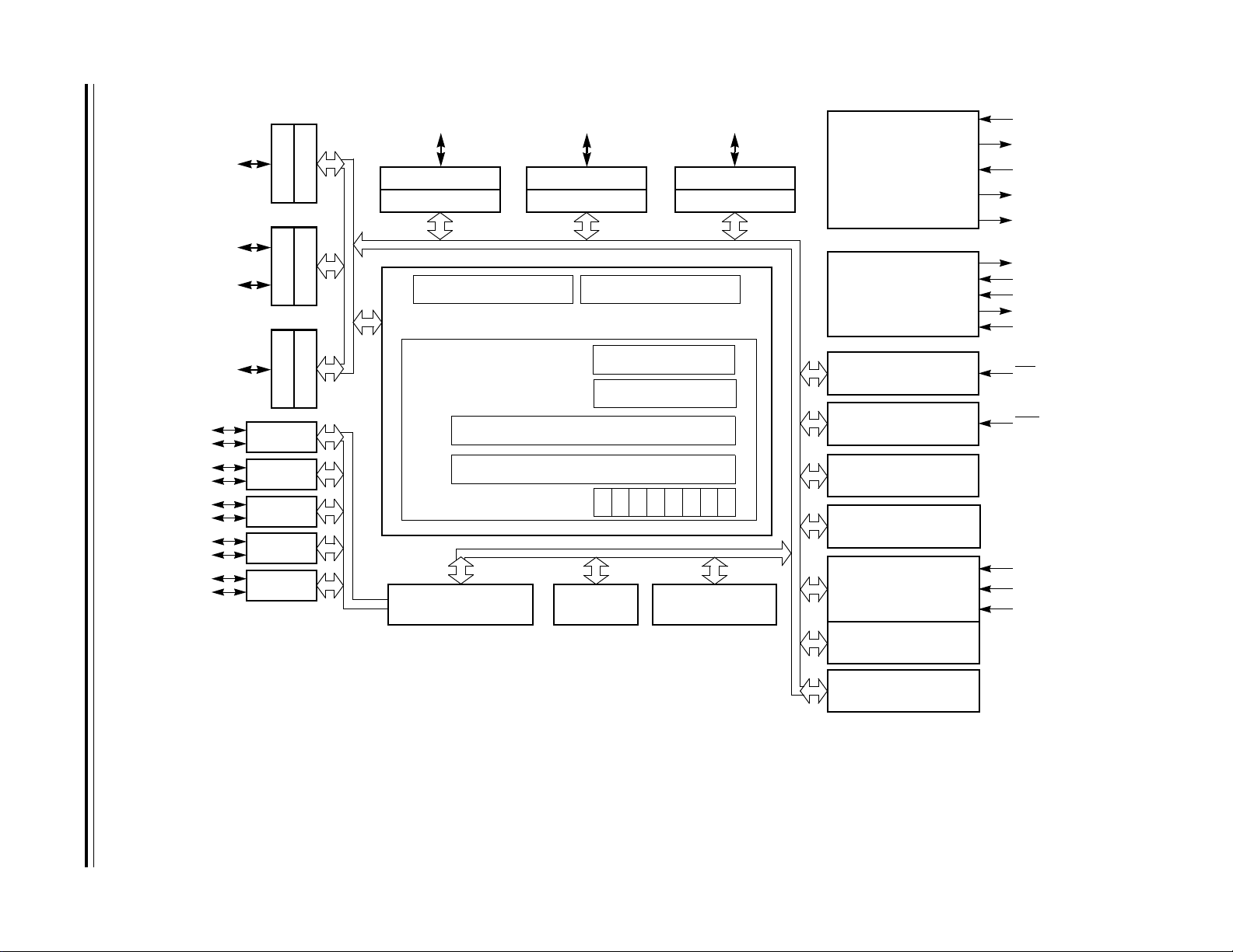
Figure 1-1 shows the structure of the MC68HC(7)08KH12.
Advance Information MC68HC(7)08KH12 — Rev. 1.1
26 Freescale Semiconductor
Page 27
Freescale Semiconductor
MC68HC(7)08KH12 — Rev. 1.1 Advance Information
PTD7/KBD7–
PTD0/KBD0
PTE3/KBE3–
PTE0/KBE0
PTF7/KBF7–
PTF0/KBF0
DPLUS4
DMINUS4
DPLUS3
DMINUS3
DPLUS2
DMINUS2
DPLUS1
DMINUS1
DPLUS0
DMINUS0
PTE4
➀➃➅
➀➃
PTC4–PTC0
➄
DS Port 4
DS Port 3
DS Port 2
DS Port 1
PORT D
PORT E
PORT F
US Port
DDRD
DDRE
DDRF
PORT C
DDRC
Embedded USB Function 384 bytes RAM 12k-bytes ROM/OTPROM
➀➁
CPU CONTROL ALU
CPU REGISTERS
CONDITION CODE REGISTER
PTB7–PTB0
PORT B
68HC08 CPU
STACK POINTER
PROGRAM COUNTER
➀
DDRB
ACCUMULATOR
INDEX REGISTER
V11H I NZ C
PTA7–PTA0
PORT A
DDRA
POWER SUPPLY
AND
VOLTAGE REGULATION
CLOCK GENERATION
MODULE AND PLL
SYSTEM INTEGRATION
MODULE
IRQ MODULE
BREAK MODULE
POWER-ON RESET
MODULE
TIMER INTERFACE
MODULE
VDD1
VSS1
VDD2
VSS2
REGOUT
OSC2
OSC1
VDDA
VSSA
CGMXFC
➂
RST
IRQ1/VPP
TCLK/PTE0
TCH0/PTE1
TCH1/PTE2
➂➃
27
➀ PORTS ARE SOFTWARE CONFIGURABLE WITH PULLUP DEVICE IF INPUT PORT
➁ SOFTWARE CONFIGURABLE LED DIRECT DRIVE 3mA SOURCE /10mA SINK or STANDARD DRIVE
➂ PIN CONTAINS INTEGRATED PULLUP DEVICE
➃ PIN HAS INTERRUPT CAPABILITY
➄ PIN HAS INTERRUPT AND INTEGRATED PULLUP DEVICE.
➅ PIN HAS OPTICAL COUPLING INTERFACE
Figure 1-1. MCU Block Diagram
COP MODULE
MONITOR ROM
240 bytes
Page 28
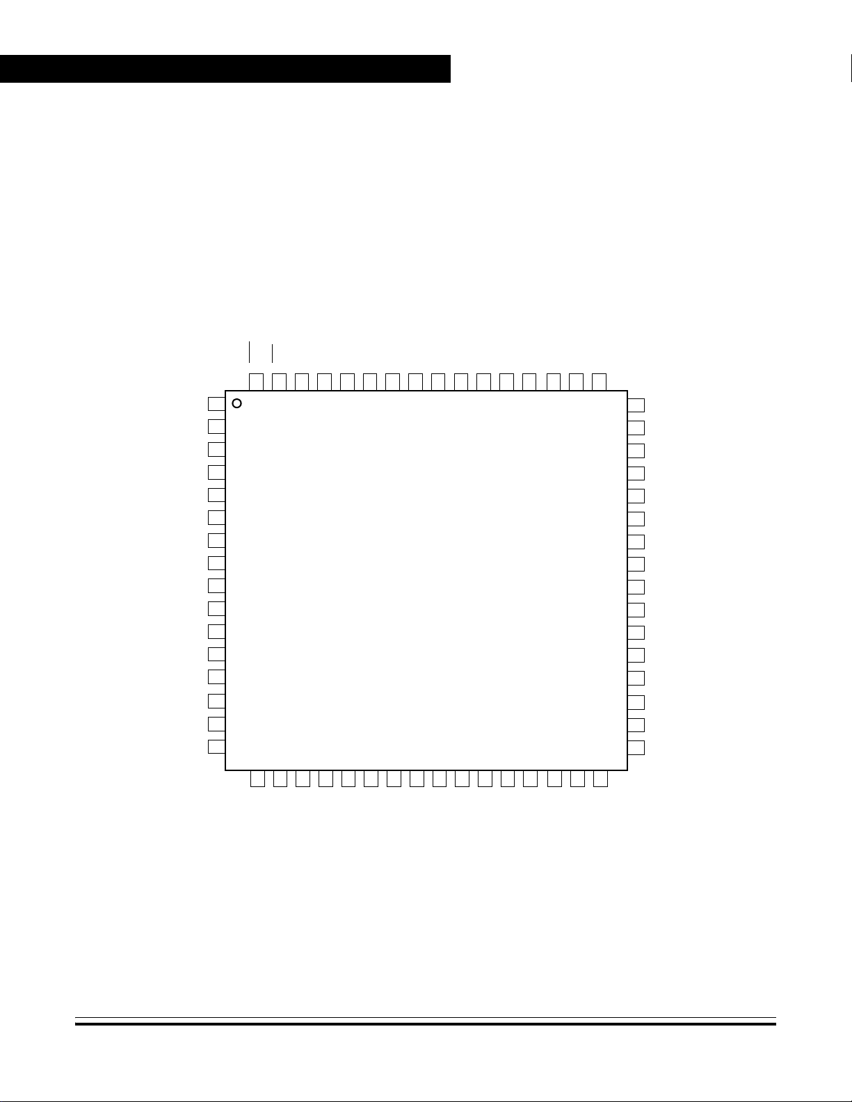
1.5 Pin Assignments
1.5.1 Quad Flat Pack (QFP) Package
Figure 1-2 Shows the 64-pin QFP assignments.
PTF0/KBF0
RST
IRQ1/VPP
64
63
VDDA
CGMXFC
OSC1
OSC2
VSSA
REGOUT
DPLUS0
DMINUS0
DPLUS1
DMINUS1
DPLUS2
DMINUS2
DPLUS3
DMINUS3
DPLUS4
DMINUS4
1
2
3
4
5
6
7
8
9
10
11
12
13
14
15
16
17
62
18
19
PTF5/KBF5
PTF4/KBF4
PTF3/KBF3
PTF2/KBF2
PTF1/KBF1
61
60
59
58
57
68HC(7)08KH12
20
21
22
23
24
PTF6/KBF6
PTF7/KBF7
56
55
25
VSS2
VDD2
PTA7
PTA6
PTA5
PTA4
54
53
52
51
26
27
28
30
29
49
50
48
47
46
45
44
42
42
41
40
39
38
37
36
35
34
33
31
32
PTA3
PTA2
PTA1
PTA0
PTB7
PTB6
PTB5
PTB4
PTB3
PTB2
PTB1
PTB0
PTD7/KBD7
PTD6/KBD6
PTD5/KBD5
PTD4/KBD4
PTE4
VSS1
PTE3/KBE3
PTE0/KBE0/TCLK
PTE1/KBE1/TCH0
PTE2/KBE2/TCH1
VDD1
PTC0
PTC1
PTC2
PTC3
PTC4
PTD0/KBD0
PTD1/KBD1
PTD2/KBD2
PTD3/KBD3
Figure 1-2. 64-Pin QFP Assignments (Top View)
Advance Information MC68HC(7)08KH12 — Rev. 1.1
28 Freescale Semiconductor
Page 29
1.5.2 Power Supply Pins (V
V
DDA
the on-chip Phase-Locked Loop circuit.
V
DD2
internal circuitry of the chip.
V
DD1
The MCU operates from a single power supply.
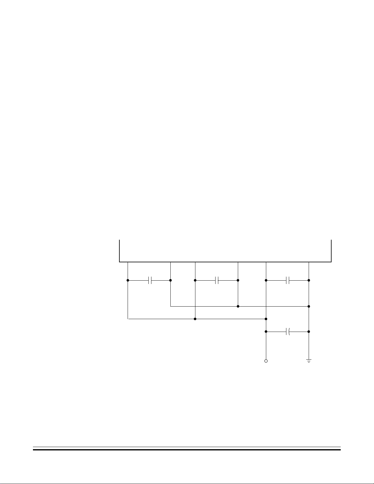
Fast signal transitions on MCU pins place high, short-duration current
demands on the power supply. To prevent noise problems, take special
care to provide power supply bypassing at the MCU as Figure 1-3
shows. Place the bypass capacitors as close to the MCU power pins as
possible. Use high-frequency-response ceramic capacitors for C
C
BULK
that require the port pins to source high current levels.
, V
DDA
and V
and V
and V
, V
SSA
are the analog power supply and ground pins used by
SSA
are the power supply and ground pins used by the
SS2
are the power supply and ground pins to the I/O pads.
SS1
DD1
, V
SS1
, V
DD2
, and V
SS2
)
BYPASS
are optional bulk current bypass capacitors for use in applications
.
V
DDA
C
BYPASS
10nF
NOTE: Values shown are typical values.
V
SSA
Figure 1-3. Power Supply Bypassing
MCU
V
DD2
C
BYPASS
10nF
V
SS2
V
DD2
Vbus
C
BYPASS
10nF
+
C
BULK
V
SS1
MC68HC(7)08KH12 — Rev. 1.1 Advance Information
Freescale Semiconductor
29
Page 30

1.5.3 Oscillator Pins (OSC1 and OSC2)
The OSC1 and OSC2 pins are the connections for the on-chip oscillator
circuit. (See Section 8. Clock Generator Module (CGM).)
1.5.4 External Reset Pin (RST)
A logic zero on the RST pin forces the MCU to a known start-up state.
RST is bidirectional, allowing a reset of the entire system. It is driven low
when any internal reset source is asserted. The RST pin contains an
internal pullup device. ((See Section 7. System Integration Module
(SIM).)
1.5.5 External Interrupt Pin (IRQ1/VPP)
IRQ1/VPP is an asynchronous external interrupt pin. IRQ1/VPP is also
the OTPROM programming power pin. The IRQ1/V
internal pullup device. (See Section 14. External Interrupt (IRQ).)
pin contain an
PP
1.5.6 USB Data Pins (DPLUS0–DPLUS4 and DMINUS0–DMINUS4)
DPLUS0–DPLUS4 and DMINUS0–DMINUS4 are the differential data
lines used by the USB module. (See Section 9. Universal Serial Bus
Module (USB).)
1.5.7 Voltage Regulator Out (REGOUT)
REGOUT is the 3.3V output of the on-chip voltage regulator. It is used to
supply the voltage for the external pullup resistor required by the USB on
either DPLUS or DMINUS lines, depending on type of USB function.
REGOUT is also used internally for the USB data driver and the Phaselocked Loop circuit. The REGOUT pin requires an external bulk
capacitor 1µF or larger and a bypass capacitor. (See Section 9.
Universal Serial Bus Module (USB).)
Advance Information MC68HC(7)08KH12 — Rev. 1.1
30 Freescale Semiconductor
Page 31

1.5.8 Port A Input/Output (I/O) Pins (PTA7–PTA0)
PTA7–PTA0 are general-purpose bidirectional I/O port pins. (See
Section 12. I/O Ports.) Each pin contains a software configurable pull-
up device when the pin is configured as an input. (See 12.9 Port
Options.)
1.5.9 Port B I/O Pins (PTB7–PTB0)
PTB7–PTB0 are general-purpose bidirectional I/O port pins. (See
Section 12. I/O Ports.) Each pin contains a software configurable pull-
up device when the pin is configured as an input. (See 12.9 Port
Options.)
1.5.10 Port C I/O Pins (PTC4–PTC0)
PTC4–PTC0 are general-purpose bidirectional I/O port pins. (See
Section 12. I/O Ports.) Port C pins are software configurable to be LED
Direct Drive ports. Each pin contains a software configurable pull-up
device when the pin is configured as an input. (See 12.9 Port Options.)
1.5.11 Port D I/O Pins (PTD7/KBD7–PTD0/KBD0)
PTD7/KBD7–PTD0/KBD0 are general-purpose bidirectional I/O port
pins. (See Section 12. I/O Ports.) Any or all of the port D pins can be
programmed to serve as external interrupt pins. (See Section 15.
Keyboard Interrupt Module (KBI).)
1.5.12 Port E I/O Pins (PTE4, PTE3/KBE3, PTE2/KBE2/TCH1, PTE1/KBE1/TCH0, PTE0/KBE0/TCLK)
Port-E is a 5-bit special function port which shares three of its pins with
the Timer Interface Module and four of its pins with Keyboard Interrupt
Module (see Section 12. I/O Ports, Section 15. Keyboard Interrupt
Module (KBI) and Section 11. Timer Interface Module (TIM)). In
addition, PTE3-PTE0 has built-in optical coupling interface for optical
mouse application. (See Section 12. I/O Ports.)
MC68HC(7)08KH12 — Rev. 1.1 Advance Information
Freescale Semiconductor
31
Page 32

1.5.13 Port F I/O Pins (PTF7/KBF7–PTF0/KBF0)
PTF7/KBF7–PTF0/KBF0 are general-purpose bidirectional I/O port pins.
(See Section 12. I/O Ports.) Any or all of the port F pins can be
programmed to serve as external interrupt pins. (See Section 15.
Keyboard Interrupt Module (KBI).)
Advance Information MC68HC(7)08KH12 — Rev. 1.1
32 Freescale Semiconductor
Page 33

Advance Information — MC68HC(7)08KH12
2.1 Contents
2.2 Introduction. . . . . . . . . . . . . . . . . . . . . . . . . . . . . . . . . . . . . . . .33
2.3 I/O Section . . . . . . . . . . . . . . . . . . . . . . . . . . . . . . . . . . . . . . . .35
2.4 Monitor ROM . . . . . . . . . . . . . . . . . . . . . . . . . . . . . . . . . . . . . .43
2.2 Introduction
The CPU08 can address 64 Kbytes of memory space. The memory
map, shown in Figure 2-1, includes:
Section 2. Memory Map
• 11776 bytes of ROM or OTPROM
• 384 bytes of RAM
• 26 bytes of user-defined vectors
• 240 bytes of Monitor ROM
MC68HC(7)08KH12 — Rev. 1.1 Advance Information
Freescale Semiconductor
33
Page 34

$0000
↓
$005F
$0060
↓
$01DF
$01E0
↓
$CDFF
$D000
↓
$FDFF
$FE00 BREAK STATUS REGISTER (BSR)
$FE01 RESET STATUS REGISTER (RSR)
$FE02 RESERVED
$FE03 BREAK FLAG CONTROL REGISTER (BFCR)
$FE04 INTERRUPT STATUS REGISTER 1 (INT1)
$FE05 INTERRUPT STATUS REGISTER 2 (INT2)
$FE06 RESERVED
$FE07 RESERVED
$FE08
↓
$FE0B
$FE0C BREAK ADDRESS HIGH REGISTER (BRKH)
$FE0D BREAK ADDRESS LOW REGISTER (BRKL)
$FE0E BREAK STATUS AND CONTROL REGISTER (BSCR)
$FE0F RESERVED
$FE10
↓
$FEFF
$FF00
↓
$FF8D RESERVED
↓
$FFE5
$FFE6
↓
$FFFF
I/O REGISTERS (80 BYTES)
RAM (384 BYTES)
UNIMPLEMENTED (52, 256 BYTES)
ROM/OTPROM (11776 BYTES)
RESERVED (4 BYTES)
MONITOR ROM (240 BYTES)
$FF00 to $FF8C
UNIMPLEMENTED (141 BYTES)
$FF8E to $FFE5
UNIMPLEMENTED (88 BYTES)
VECTORS (26 BYTES)
Figure 2-1. Memory Map
Advance Information MC68HC(7)08KH12 — Rev. 1.1
34 Freescale Semiconductor
Page 35

2.3 I/O Section
Addresses $0000–$005F, shown in Figure 2-2, contain most of the
control, status, and data registers. Additional I/O registers have the
following addresses:
• $FE00 (Break Status Register, BSR)
• $FE01 (Reset Status Register, RSR)
• $FE02 (Reserved)
• $FE03 (Break Flag Control Register, BFCR)
• $FE04 (Interrupt Status Register 1, INT1)
• $FE05 (Interrupt Status Register 2, INT2)
• $FE06 (Reserved)
• $FE07 (Reserved)
• $FE08 (Reserved)
• $FE09 (Reserved)
• $FE0A (Reserved)
• $FE0B (Reserved)
• $FE0C and $FE0D (Break Address Registers, BRKH and BRKL)
• $FE0E (Break Status and Control Register, BSCR)
• $FF8D (Reserved)
• $FFFF (COP Control Register, COPCTL)
MC68HC(7)08KH12 — Rev. 1.1 Advance Information
Freescale Semiconductor
35
Page 36

Addr. Name Bit 7654321Bit 0
$0000 Port A Data Register (PTA)
$0001 Port B Data Register (PTB)
$0002 Port C Data Register (PTC)
$0003 Port D Data Register (PTD)
$0004 Data Direction Register A (DDRA)
$0005 Data Direction Register B (DDRB)
$0006 Data Direction Register C (DDRC)
$0007 Data Direction Register D (DDRD)
$0008 Port E Data Register (PTE)
$0009 Port F Data Register (PTF)
$000A Data Direction Register E (DDRE)
$000B Data Direction Register F (DDRF)
$000C
$000D
$000E
$000F
Port D Keyboard Status and
Control Register (KBDSCR)
Port D Keyboard Interrupt Enable
Register (KBDIER)
Port E Keyboard Status and
Control Register (KBESCR)
Port E Keyboard Interrupt Enable
Register (KBEIER)
R:
PTA7 PTA6 PTA5 PTA4 PTA3 PTA2 PTA1 PTA0
W:
R:
PTB7 PTB6 PTB5 PTB4 PTB3 PTB2 PTB1 PTB0
W:
R:000
W:
R:
PTD7 PTD6 PTD5 PTD4 PTD3 PTD2 PTD1 PTD0
W:
R:
DDRA7 DDRA6 DDRA5 DDRA4 DDRA3 DDRA2 DDRA1 DDRA0
W:
R:
DDRB7 DDRB6 DDRB5 DDRB4 DDRB3 DDRB2 DDRB1 DDRB0
W:
R:000
W:
R:
DDRD7 DDRD6 DDRD5 DDRD4 DDRD3 DDRD2 DDRD1 DDRD0
W:
R:000
W:
R:
PTF7 PTF6 PTF5 PTF4 PTF3 PTF2 PTF1 PTF0
W:
R:000
W:
R:
DDRF7 DDRF6 DDRF5 DDRF4 DDRF3 DDRF2 DDRF1 DDRF0
W:
R:0000KEYDF0
W:
R: KBDIE7 KBDIE6 KBDIE5 KBDIE4 KBDIE3 KBDIE2 KBDIE1 KBDIE0
R:0000KEYEF 0
W:
R:
PEPE3 PEPE2 PEPE1 PEPE0 KBEIE3 KBEIE2 KBEIE1 KBEIE0
W:
PTC4 PTC3 PTC2 PTC1 PTC0
DDRC4 DDRC3 DDRC2 DDRC1 DDRC0
PTE4 PTE3 PTE2 PTE1 PTE0
DDRE4 DDRE3 DDRE2 DDRE1 DDRE0
ACKD
ACKE
IMASKD MODED
IMASKE MODEE
= Unimplemented R = Reserved
Figure 2-2. Control, Status, and Data Registers
Advance Information MC68HC(7)08KH12 — Rev. 1.1
36 Freescale Semiconductor
Page 37

Addr. Name Bit 7654321Bit 0
$0010
$0011 Unimplemented
$0012
$0013
$0014
$0015
$0016
$0017
$0018
$0019
$001A
$001B
$001C
$001D Port Option Control Register (POC)
$001E
$001F
TIM Status and Control Register
(TSC)
TIM Counter Register High
(TCNTH)
TIM Counter Register Low
(TCNTL)
TIM Counter Modulo Register High
(TMODH)
TIM Counter Modulo Register Low
(TMODL)
TIM Channel 0 Status and Control
Register (TSC0)
TIM Channel 0 Register High
(TCH0H)
TIM Channel 0 Register Low
(TCH0L)
TIM Channel 1 Status and Control
Register (TSC1)
TIM Channel 1 Register High
(TCH1H)
TIM Channel 1 Register Low
(TCH1L)
PORT E Optical Interface Enable
Register (EOIER)
IRQ Status and Control Register
(ISCR)
Configuration Register
(CONFIG)
† One-time writable register
R: TOF
W: 0 TRST
R:
W:
R: Bit 15 14 13 12 11 10 9 Bit 8
W:
R:Bit 7654321Bit 0
W:
R:
Bit 15 14 13 12 11 10 9 Bit 8
W:
R:
Bit 7654321Bit 0
W:
R: CH0F
W: 0
R:
Bit 15 14 13 12 11 10 9 Bit 8
W:
R:
Bit 7654321Bit 0
W:
R: CH1F
W: 0
R: Bit 15 14 13 12 11 10 9 Bit 8
R:Bit 7654321Bit 0
W:
R:
YREF2 YREF1 YREF0 XREF2 XREF1 XREF0 OIEY OIEX
W:
R: 0 0
W:
R:0000IRQF10
W
R:0000
†
W:
TOIE TSTOP
CH0IE MS0B MS0A ELS0B ELS0A TOV0 CH0MAX
CH1IE
0
LDD
00
MS1A ELS1B ELS1A TOV1 CH1MAX
00
SSREC COPRS STOP COPD
PS2 PS1 PS0
PCP PBP PAP
ACK1
IMASK1 MODE1
= Unimplemented R = Reserved
Figure 2-2. Control, Status, and Data Registers (Continued)
MC68HC(7)08KH12 — Rev. 1.1 Advance Information
Freescale Semiconductor
37
Page 38

Addr. Name Bit 7654321Bit 0
$0020
$0021
$0022
$0023
$0024
$0025
$0026
$0027
$0028
$0029
$002A
$002B
$002C
$002D
$002E
$002F
USB Embedded Device Endpoint 0
Data Register 0 (DE0D0)
USB Embedded Device Endpoint 0
Data Register 1 (DE0D1)
USB Embedded Device Endpoint 0
Data Register 2 (DE0D2)
USB Embedded Device Endpoint 0
Data Register 3 (DE0D3)
USB Embedded Device Endpoint 0
Data Register 4 (DE0D4)
USB Embedded Device Endpoint 0
Data Register 5 (DE0D5)
USB Embedded Device Endpoint 0
Data Register 6 (DE0D6)
USB Embedded Device Endpoint 0
Data Register 7 (DE0D7)
USB Embedded Device Endpoint
1/2 Data Register 0 (DE1D0)
USB Embedded Device Endpoint
1/2 Data Register 1 (DE1D1)
USB Embedded Device Endpoint
1/2 Data Register 2 (DE1D2)
USB Embedded Device Endpoint
1/2 Data Register 3 (DE1D3)
USB Embedded Device Endpoint
1/2 Data Register 4 (DE1D4)
USB Embedded Device Endpoint
1/2 Data Register 5 (DE1D5)
USB Embedded Device Endpoint
1/2 Data Register 6 (DE1D6)
USB Embedded Device Endpoint
1/2 Data Register 7 (DE1D7)
R: DE0R07 DE0R06 DE0R05 DE0R04 DE0R03 DE0R02 DE0R01 DE0R00
W: DE0T07 DE0T06 DE0T05 DE0T04 DE0T03 DE0T02 DE0T01 DE0T00
R: DE0R17 DE0R16 DE0R15 DE0R14 DE0R13 DE0R12 DE0R11 DE0R10
W: DE0T17 DE0T16 DE0T15 DE0T14 DE0T13 DE0T12 DE0T11 DE0T10
R: DE0R27 DE0R26 DE0R25 DE0R24 DE0R23 DE0R22 DE0R21 DE0R20
W: DE0T27 DE0T26 DE0T25 DE0T24 DE0T23 DE0T22 DE0T21 DE0T20
R: DE0R37 DE0R36 DE0R35 DE0R34 DE0R33 DE0R32 DE0R31 DE0R30
W: DE0T37 DE0T36 DE0T35 DE0T34 DE0T33 DE0T32 DE0T31 DE0T30
R: DE0R47 DE0R46 DE0R45 DE0R44 DE0R43 DE0R42 DE0R41 DE0R40
W: DE0T47 DE0T46 DE0T45 DE0T44 DE0T43 DE0T42 DE0T41 DE0T40
R: DE0R57 DE0R56 DE0R55 DE0R54 DE0R53 DE0R52 DE0R51 DE0R50
W: DE0T57 DE0T56 DE0T55 DE0T54 DE0T53 DE0T52 DE0T51 DE0T50
R: DE0R67 DE0R66 DE0R65 DE0R64 DE0R63 DE0R62 DE0R61 DE0R60
W: DE0T67 DE0T66 DE0T65 DE0T64 DE0T63 DE0T62 DE0T61 DE0T60
R: DE0R77 DE0R76 DE0R75 DE0R74 DE0R73 DE0R72 DE0R71 DE0R70
W: DE0T77 DE0T76 DE0T75 DE0T74 DE0T73 DE0T72 DE0T71 DE0T70
R:
W: DE1T07 DE1T06 DE1T05 DE1T04 DE1T03 DE1T02 DE1T01 DE1T00
R:
W: DE1T17 DE1T16 DE1T15 DE1T14 DE1T13 DE1T12 DE1T11 DE1T10
R:
W: DE1T27 DE1T26 DE1T25 DE1T24 DE1T23 DE1T22 DE1T21 DE1T20
R:
W: DE1T37 DE1T36 DE1T35 DE1T34 DE1T33 DE1T32 DE1T31 DE1T30
R:
W: DE1T47 DE1T46 DE1T45 DE1T44 DE1T43 DE1T42 DE1T41 DE1T40
R:
W: DE1T57 DE1T56 DE1T55 DE1T54 DE1T53 DE1T52 DE1T51 DE1T50
R:
W: DE1T67 DE1T66 DE1T65 DE1T64 DE1T63 DE1T62 DE1T61 DE1T60
R:
W: DE1T77 DE1T76 DE1T75 DE1T74 DE1T73 DE1T72 DE1T71 DE1T70
= Unimplemented R = Reserved
Figure 2-2. Control, Status, and Data Registers (Continued)
Advance Information MC68HC(7)08KH12 — Rev. 1.1
38 Freescale Semiconductor
Page 39

Addr. Name Bit 7654321Bit 0
$0030
$0031
$0032
$0033
$0034
$0035
$0036
$0037
$0038 Unimplemented
$0039 Unimplemented
$003A
$003B
$003C
$003D
$003E Unimplemented
$003F
USB HUB Endpoint 0 Data
Register 0 (HE0D0)
USB HUB Endpoint 0 Data
Register 1 (HE0D1)
USB HUB Endpoint 0 Data
Register 2 (HE0D2)
USB HUB Endpoint 0 Data
Register 3 (HE0D3)
USB HUB Endpoint 0 Data
Register 4 (HE0D4)
USB HUB Endpoint 0 Data
Register 5 (HE0D5)
USB HUB Endpoint 0 Data
Register 6 (HE0D6)
USB HUB Endpoint 0 Data
Register 7 (HE0D7)
PLL Control Register
(PCTL)
PLL Bandwidth Control Register
(PBWC)
PLL Multiplier Select Register High
(PMSH)
PLL Multiplier Select Register Low
(PMSL)
PLL Reference Divider Select
Register (PRDS)
R: HE0R07 HE0R06 HE0R05 HE0R04 HE0R03 HE0R02 HE0R01 HE0R00
W: HE0T07 HE0T06 HE0T05 HE0T04 HE0T03 HE0T02 HE0T01 HE0T00
R: HE0R17 HE0R16 HE0R15 HE0R14 HE0R13 HE0R12 HE0R11 HE0R10
W: HE0T17 HE0T16 HE0T15 HE0T14 HE0T13 HE0T12 HE0T11 HE0T10
R: HE0R27 HE0R26 HE0R25 HE0R24 HE0R23 HE0R22 HE0R21 HE0R20
W: HE0T27 HE0T26 HE0T25 HE0T24 HE0T23 HE0T22 HE0T21 HE0T20
R: HE0R37 HE0R36 HE0R35 HE0R34 HE0R33 HE0R32 HE0R31 HE0R30
W: HE0T37 HE0T36 HE0T35 HE0T34 HE0T33 HE0T32 HE0T31 HE0T30
R: HE0R47 HE0R46 HE0R45 HE0R44 HE0R43 HE0R42 HE0R41 HE0R40
W: HE0T47 HE0T46 HE0T45 HE0T44 HE0T43 HE0T42 HE0T41 HE0T40
R: HE0R57 HE0R56 HE0R55 HE0R54 HE0R53 HE0R52 HE0R51 HE0R50
W: HE0T57 HE0T56 HE0T55 HE0T54 HE0T53 HE0T52 HE0T51 HE0T50
R: HE0R67 HE0R66 HE0R65 HE0R64 HE0R63 HE0R62 HE0R61 HE0R60
W: HE0T67 HE0T66 HE0T65 HE0T64 HE0T63 HE0T62 HE0T61 HE0T60
R: HE0R77 HE0R76 HE0R75 HE0R74 HE0R73 HE0R72 HE0R71 HE0R70
W: HE0T77 HE0T76 HE0T75 HE0T74 HE0T73 HE0T72 HE0T71 HE0T70
R:
W:
R:
W:
R:
PLLIE
W:
R:
AUTO
W:
R:
W:
R:
MUL7 MUL6 MUL5 MUL4 MUL3 MUL2 MUL1 MUL0
W:
R:
W:
R:
W:
PLLF
LOCK
PLLON BCS
ACQ
00000
PRE1 PRE0 0 0
MUL11 MUL10 MUL9 MUL8
RDS3 RDS2 RDS1 RDS0
= Unimplemented R = Reserved
Figure 2-2. Control, Status, and Data Registers (Continued)
MC68HC(7)08KH12 — Rev. 1.1 Advance Information
Freescale Semiconductor
39
Page 40

Addr. Name Bit 7654321Bit 0
$0040
$0041
$0042
$0043 Unimplemented
$0044 Unimplemented
$0045 Unimplemented
$0046 Unimplemented
$0047
$0048
$0049
$004A
$004B
$004C
$004D
$004E Unimplemented
$004F Unimplemented
Port F Keyboard Status and Control
Register (KBFSCR)
Port F Keyboard Interrupt Enable
Register (KBFIER)
Port F Pull-up Enable Register
USB Embedded Device Control
Register 2 (DCR2)
USB Embedded Device Address
Register (DADDR)
USB Embedded Device Interrupt
Register 0 (DIR0)
USB Embedded Device Interrupt
Register 1 (DIR1)
USB Embedded Device Control
Register 0 (DCR0)
USB Embedded Device Control
Register 1 (DCR1)
USB Embedded Device Status
Register (DSR)
(PFPER)
R:0000KEYFF 0
W:
R:
KBFIE7 KBFIE6 KBFIE5 KBFIE4 KBFIE3 KBFIE2 KBFIE1 KBFIE0
W:
R:
PFPE7 PFPE6 PFPE5 PFPE4 PFPE3 PFPE2 PFPE1 PFPE0
W:
R:
W:
R:
W:
R:
W:
R:
W:
R:0000
W:
R:
DEVEN DADD6 DADD5 DADD4 DADD3 DADD2 DADD1 DADD0
W:
R: TXD0F RXD0F 0 0
W:
R: TXD1F 0 0 0
W:
R:
T0SEQ DSTALL0 TX0E RX0E TP0SIZ3 TP0SIZ2 TP0SIZ1 TP0SIZ0
W:
R:
T1SEQ ENDADD TX1E
W:
R: DRSEQ DSETUP DTX1ST 0 RP0SIZ3 RP0SIZ2 RP0SIZ1 RP0SIZ0
W:
R:
W:
R:
W:
DTX1STR
ENABLE2 ENABLE1 DSTALL2
TXD0IE RXD0IE
TXD1IE
0
TP1SIZ3 TP1SIZ2 TP1SIZ1 TP1SIZ0
ACKF
IMASKF MODEF
DSTALL1
00
TXD0FR RXD0FR
000
TXD1FR
= Unimplemented R = Reserved
Figure 2-2. Control, Status, and Data Registers (Continued)
Advance Information MC68HC(7)08KH12 — Rev. 1.1
40 Freescale Semiconductor
Page 41

Addr. Name Bit 7654321Bit 0
$0050 Unimplemented
$0051
$0052
$0053
$0054
$0055 Unimplemented
$0056
$0057
$0058
$0059
$005A Unimplemented
$005B
$005C
$005D USB HUB Status Register (HSR)
$005E
$005F Unimplemented
USB HUB Downstream Port 1
Control Register (HDP1CR)
USB HUB Downstream Port 2
Control Register (HDP2CR)
USB HUB Downstream Port 3
Control Register (HDP3CR)
USB HUB Downstream Port 4
Control Register (HDP4CR)
USB SIE Timing Interrupt Register
(SIETIR)
USB SIE Timing Status Register
(SIETSR)
USB HUB Address Register
(HADDR)
USB HUB Interrupt Register 0
(HIR0)
USB HUB Control Register 0
(HCR0)
USB HUB Endpoint1 Control &
Data Register (HCDR)
USB HUB Root Port Control
Register (HRPCR)
R:
W:
R:
PEN1 LOWSP1 RST1 RESUM1 SUSP1
W:
R:
PEN2 LOWSP2 RST2 RESUM2 SUSP2
W:
R:
PEN3 LOWSP3 RST3 RESUM3 SUSP3
W:
R:
PEN4 LOWSP4 RST4 RESUM4 SUSP4
W:
R:
W:
R: SOFF EOF2F EOPF TRANF
W:
R:RSTF0LOCKF00000
W:
R:
USBEN ADD6 ADD5 ADD4 ADD3 ADD2 ADD1 ADD0
W:
R: TXDF RXDF 0 0
W:
R:
W:
R:
TSEQ STALL0 TXE RXE TPSIZ3 TPSIZ2 TPSIZ1 TPSIZ0
W:
R:
STALL1 PNEW PCHG5 PCHG4 PCHG3 PCHG2 PCHG1 PCHG0
W:
R: RSEQ SETUP TX1ST 0 RPSIZ3 RPSIZ2 RPSIZ1 RPSIZ0
W:
R:000
W:
R:
W:
RSTFR LOCKFR SOFFR EOF2FR EOPFR TRANFR
TX1STR
RESUM0 SUSPND
SOFIE EOF2IE EOPIE TRANIE
TXDIE RXDIE
0D1+D1–
0D2+D2–
0D3+D3–
0D4+D4–
00
TXDFR RXDFR
0D0+D0–
= Unimplemented R = Reserved
Figure 2-2. Control, Status, and Data Registers (Continued)
MC68HC(7)08KH12 — Rev. 1.1 Advance Information
Freescale Semiconductor
41
Page 42

Addr. Name Bit 7654321Bit 0
$FE00
$FE01
$FE02 Reserved
$FE03
$FE04 Interrupt Status Register 1 (INT1)
$FE05 Interrupt Status Register 2 (INT2)
$FE06 Reserved
$FE07 Reserved
$FE08 Unimplemented
Break Status Register
Reset Status Register
Break Flag Control Register
$FE09 Unimplemented
$FE0A Unimplemented
$FE0B Unimplemented
$FE0C
$FE0D
$FE0E
Break Address Register High
Break Address Register Low
Break Status and Control Register
(BFCR)
(BRKH)
(BRKL)
(BRKSCR)
R:
(BSR)
(RSR)
RRRRRRSBSW R
W:
R: POR PIN COP ILOP ILAD USB 0 0
W:
R:
W:
R:
BCFERRRRRRR
W:
R: IF6 IF5 IF4 IF3 IF2 IF1 0 0
W:RRRRRRRR
R: 0 0 0 IF11 IF10 IF9 IF8 IF7
W:RRRRRRRR
R:
W:
R:
W:
R:
W:
R:
W:
R:
W:
R:
W:
R:
Bit 15 14 13 12 11 10 9 Bit 8
W:
R:
Bit 7654321Bit 0
W:
R:
BRKE BRKA
W:
000000
$FF8D Reserved
$FFFF
COP Control Register
(COPCTL)
R:
W:
R: Low byte of reset vector
W: Writing clears COP counter (any value)
= Unimplemented R = Reserved
Figure 2-2. Control, Status, and Data Registers (Continued)
Advance Information MC68HC(7)08KH12 — Rev. 1.1
42 Freescale Semiconductor
Page 43

Table 2-1 is a list of vector locations.
Table 2-1. Vector Addresses
Address Vector
$FFE6 PLL Vector (High)
$FFE7 PLL Vector (Low)
$FFE8 Port-F Keyboard Vector (High)
$FFE9 Port-F Keyboard Vector (Low)
$FFEA Port-D Keyboard Vector (High)
$FFEB Port-D Keyboard Vector (Low)
$FFEC Port-E Keyboard Vector (High)
$FFED Port-E Keyboard Vector (Low)
$FFEE TIM Overflow Vector (High)
$FFEF TIM Overflow Vector (Low)
$FFF0 TIM Channel 1 Vector (High)
$FFF1 TIM Channel 1 Vector (Low)
Priority LowHigh
$FFF2 TIM Channel 0 Vector (High)
$FFF3 TIM Channel 0 Vector (Low)
$FFF4 USB Device Endpoint Interrupt Vector (High)
$FFF5 USB Device Endpoint Interrupt Vector (Low)
$FFF6 USB HUB Endpoint Interrupt Vector (High)
$FFF7 USB HUB Endpoint Interrupt Vector (Low)
$FFF8 USB SIE Timing Interrupt Vector (High)
$FFF9 USB SIE Timing Interrupt Vector (Low)
$FFFA IRQ1 Vector (High)
$FFFB IRQ1 Vector (Low )
$FFFC SWI Vector (High)
$FFFD SWI Vector (Low)
$FFFE Reset Vector (High)
$FFFF Reset Vector (Low)
2.4 Monitor ROM
The 240 bytes at addresses $FE10–$FEFF are reserved ROM
addresses that contain the instructions for the monitor functions. (See
Section 10. Monitor ROM (MON).)
MC68HC(7)08KH12 — Rev. 1.1 Advance Information
Freescale Semiconductor
43
Page 44

Advance Information MC68HC(7)08KH12 — Rev. 1.1
44 Freescale Semiconductor
Page 45

Advance Information — MC68HC(7)08KH12
Section 3. Random-Access Memory (RAM)
3.1 Contents
3.2 Introduction. . . . . . . . . . . . . . . . . . . . . . . . . . . . . . . . . . . . . . . .45
3.3 Functional Description . . . . . . . . . . . . . . . . . . . . . . . . . . . . . . .45
3.2 Introduction
This section describes the 384 bytes of RAM.
3.3 Functional Description
Addresses $0060 through $01DF are RAM locations. The location of the
stack RAM is programmable. The 16-bit stack pointer allows the stack to
be anywhere in the 64-Kbyte memory space.
NOTE: For correct operation, the stack pointer must point only to RAM
locations.
Within page zero are 160 bytes of RAM. Because the location of the
stack RAM is programmable, all page zero RAM locations can be used
for I/O control and user data or code. When the stack pointer is moved
from its reset location at $00FF, direct addressing mode instructions can
access efficiently all page zero RAM locations. Page zero RAM,
therefore, provides ideal locations for frequently accessed global
variables.
Before processing an interrupt, the CPU uses five bytes of the stack to
save the contents of the CPU registers.
NOTE: For M6805 compatibility, the H register is not stacked.
MC68HC(7)08KH12 — Rev. 1.1 Advance Information
Freescale Semiconductor
45
Page 46

During a subroutine call, the CPU uses two bytes of the stack to store
the return address. The stack pointer decrements during pushes and
increments during pulls.
NOTE: Be careful when using nested subroutines. The CPU may overwrite data
in the RAM during a subroutine or during the interrupt stacking
operation.
Advance Information MC68HC(7)08KH12 — Rev. 1.1
46 Freescale Semiconductor
Page 47

Advance Information — MC68HC(7)08KH12
Section 4. Read-Only Memory (ROM)
4.1 Contents
4.2 Introduction. . . . . . . . . . . . . . . . . . . . . . . . . . . . . . . . . . . . . . . .47
4.3 Functional Description . . . . . . . . . . . . . . . . . . . . . . . . . . . . . . .47
4.2 Introduction
This section describes the 11,776 bytes of read-only memory (ROM)
and 26 bytes of user vectors, available on the MC68HC08KH12 device
(ROM part).
On the MC68HC708KH12 (OTP part), the ROM is replaced with 11,776
bytes One-Time Programmable (OTP) ROM. Programming tools are
available from Freescale. Contact your local Freescale representative
for more information.
4.3 Functional Description
These addresses are user ROM locations:
$D000 – $FDFF
$FFE6 – $FFFF (These locations are reserved for user-defined interrupt
and reset vectors.)
NOTE: A secutiry feature prevents viewing of the ROM contents.
1
1. No security feature is absolutely secure. However, Freescale’s strategy is to make reading or
copying the ROM contents difficult for unauthorized users.
MC68HC(7)08KH12 — Rev. 1.1 Advance Information
Freescale Semiconductor
47
Page 48

Advance Information MC68HC(7)08KH12 — Rev. 1.1
48 Freescale Semiconductor
Page 49

Advance Information — MC68HC(7)08KH12
Section 5. Configuration Register (CONFIG)
5.1 Contents
5.2 Introduction. . . . . . . . . . . . . . . . . . . . . . . . . . . . . . . . . . . . . . . .49
5.3 Functional Description . . . . . . . . . . . . . . . . . . . . . . . . . . . . . . .49
5.2 Introduction
This section describes the configuration register (CONFIG). The
configuration register enables or disables the following options:
• Stop mode recovery time (32 CGMXCLK cycles or 4096
CGMXCLK cycles)
• STOP instruction
• Computer operating properly module (COP)
• COP reset period (COPRS), (213–24)×CGMXCLK or
(218–24)×CGMXCLK
5.3 Functional Description
The configuration register is used in the initialization of various options.
The configuration register can be written once after each reset. All of the
configuration register bits are cleared during reset. Since the various
options affect the operation of the MCU it is recommended that this
register be written immediately after reset. The configuration register is
located at $001F. The configuration register may be read at anytime.
This configuration register exists on both the MC68HC708KH12
(OTP part) and MC68HC08KH12 (ROM part).
MC68HC(7)08KH12 — Rev. 1.1 Advance Information
Freescale Semiconductor
49
Page 50

NOTE: The CONFIG register is a special register containing one-time writable
latches after each reset. Upon a reset, the CONFIG register defaults to
the predetermined settings as shown in Figure 5-1.
Address: $001F
Bit 7654321Bit 0
Read: 0000
Write:
Reset:00000000
= Unimplemented
Figure 5-1. Configuration Register (CONFIG)
SSREC — Short stop recovery bit
SSREC enables the CPU to exit stop mode with a delay of 32
CGMXCLK cycles instead of a 4096 CGMXCLK cycle delay.
1 = Stop mode recovery after 32 CGMXCLK cycles
0 = Stop mode recovery after 4096 CGMXCLK cycles
SSREC COPRS STOP COPD
NOTE: Exiting stop mode by pulling reset will result in the long stop recovery.
If using an external crystal, do not set the SSREC bit.
COPRS — COP reset period selection bit
1 = COP reset cycle is (213–24)×CGMXCLK
0 = COP reset cycle is (2
18–24
STOP — STOP instruction enable bit
STOP enables the STOP instruction.
1 = STOP instruction enabled
0 = STOP instruction treated as illegal opcode
COPD — COP disable bit
COPD disables the COP module. See Section 13. Computer
Operating Properly (COP).
1 = COP module disabled
0 = COP module enabled
)×CGMXCLK
Advance Information MC68HC(7)08KH12 — Rev. 1.1
50 Freescale Semiconductor
Page 51

Advance Information — MC68HC(7)08KH12
Section 6. Central Processor Unit (CPU)
6.1 Contents
6.2 Introduction. . . . . . . . . . . . . . . . . . . . . . . . . . . . . . . . . . . . . . . .51
6.3 Features . . . . . . . . . . . . . . . . . . . . . . . . . . . . . . . . . . . . . . . . . .52
6.4 CPU Registers . . . . . . . . . . . . . . . . . . . . . . . . . . . . . . . . . . . . .52
6.4.1 Accumulator (A). . . . . . . . . . . . . . . . . . . . . . . . . . . . . . . . . .53
6.4.2 Index Register (H:X) . . . . . . . . . . . . . . . . . . . . . . . . . . . . . .54
6.4.3 Stack Pointer (SP). . . . . . . . . . . . . . . . . . . . . . . . . . . . . . . .55
6.4.4 Program Counter (PC) . . . . . . . . . . . . . . . . . . . . . . . . . . . .56
6.4.5 Condition Code Register (CCR) . . . . . . . . . . . . . . . . . . . . .57
6.2 Introduction
6.5 Arithmetic/Logic Unit (ALU) . . . . . . . . . . . . . . . . . . . . . . . . . . .59
This section describes the central processor unit. The M68HC08 CPU is
an enhanced and fully object-code-compatible version of the M68HC05
CPU. The CPU08 Reference Manual (Freescale document number
CPU08RM/AD) contains a description of the CPU instruction set,
addressing modes, and architecture.
MC68HC(7)08KH12 — Rev. 1.1 Advance Information
Freescale Semiconductor
51
Page 52

6.3 Features
Features of the CPU include the following:
• Full Upward, Object-Code Compatibility with M68HC05 Family
• 16-Bit Stack Pointer with Stack Manipulation Instructions
• 16-Bit Index Register with X-Register Manipulation Instructions
• 8-MHz CPU Internal Bus Frequency
• 64-Kbyte Program/Data Memory Space
• 16 Addressing Modes
• Memory-to-Memory Data Moves Without Using Accumulator
• Fast 8-Bit by 8-Bit Multiply and 16-Bit by 8-Bit Divide Instructions
• Enhanced Binary-Coded Decimal (BCD) Data Handling
• Modular Architecture with Expandable Internal Bus Definition for
Extension of Addressing Range Beyond 64 Kbytes
6.4 CPU Registers
• Low-Power Stop and Wait Modes
Figure 6-1 shows the five CPU registers. CPU registers are not part of
the memory map.
Advance Information MC68HC(7)08KH12 — Rev. 1.1
52 Freescale Semiconductor
Page 53

6.4.1 Accumulator (A)
7
15
H X
15
15
70
V11HINZC
0
ACCUMULATOR (A)
0
INDEX REGISTER (H:X)
0
STACK POINTER (SP)
0
PROGRAM COUNTER (PC)
CONDITION CODE REGISTER (CCR)
CARRY/BORROW FLAG
ZERO FLAG
NEGATIVE FLAG
INTERRUPT MASK
HALF-CARRY FLAG
TWO’S COMPLEMENT OVERFLOW FLAG
Figure 6-1. CPU Registers
The accumulator is a general-purpose 8-bit register. The CPU uses the
accumulator to hold operands and the results of arithmetic/logic
operations.
Bit 7654321Bit 0
Read:
Write:
Reset: Unaffected by reset
Figure 6-2. Accumulator (A)
MC68HC(7)08KH12 — Rev. 1.1 Advance Information
Freescale Semiconductor
53
Page 54

6.4.2 Index Register (H:X)
The 16-bit index register allows indexed addressing of a 64-Kbyte
memory space. H is the upper byte of the index register, and X is the
lower byte. H:X is the concatenated 16-bit index register.
In the indexed addressing modes, the CPU uses the contents of the
index register to determine the conditional address of the operand.
Bit
15 14 13 12 11 10 9 8 7 6 5 4 3 2 1
Read:
Write:
Reset:00000000XXXXXXXX
X = Indeterminate
Bit
0
Figure 6-3. Index Register (H:X)
The index register can serve also as a temporary data storage location.
Advance Information MC68HC(7)08KH12 — Rev. 1.1
54 Freescale Semiconductor
Page 55

6.4.3 Stack Pointer (SP)
The stack pointer is a 16-bit register that contains the address of the next
location on the stack. During a reset, the stack pointer is preset to
$00FF. The reset stack pointer (RSP) instruction also sets the least
significant byte to $FF but does not affect the most significant byte. The
stack pointer decrements as data is pushed onto the stack and
increments as data is pulled from the stack.
In the stack pointer 8-bit offset and 16-bit offset addressing modes, the
stack pointer can function as an index register to access data on the
stack. The CPU uses the contents of the stack pointer to determine the
conditional address of the operand.
Bit
15 14 13 12 11 10 9 8 7 6 5 4 3 2 1
Read:
Write:
Reset:0000000011111111
Bit
0
Figure 6-4. Stack Pointer (SP)
NOTE: The location of the stack is arbitrary and may be relocated anywhere in
RAM. Moving the SP out of page zero ($0000 to $00FF) frees direct
address (page zero) space. For correct operation, the stack pointer must
point only to RAM locations.
MC68HC(7)08KH12 — Rev. 1.1 Advance Information
Freescale Semiconductor
55
Page 56

6.4.4 Program Counter (PC)
The program counter is a 16-bit register that contains the address of the
next instruction or operand to be fetched.
Normally, the program counter automatically increments to the next
sequential memory location every time an instruction or operand is
fetched. Jump, branch, and interrupt operations load the program
counter with an address other than that of the next sequential location.
During reset, the program counter is loaded with the reset vector
address located at $FFFE and $FFFF. The vector address is the
address of the first instruction to be executed after exiting the reset state.
Bit
15 14 13 12 11 10 9 8 7 6 5 4 3 2 1
Read:
Write:
Reset: Loaded with vector from $FFFE and $FFFF
Bit
0
Figure 6-5. Program Counter (PC)
Advance Information MC68HC(7)08KH12 — Rev. 1.1
56 Freescale Semiconductor
Page 57

6.4.5 Condition Code Register (CCR)
The 8-bit condition code register contains the interrupt mask and five
flags that indicate the results of the instruction just executed. Bits 6 and
5 are set permanently to logic one. The following paragraphs describe
the functions of the condition code register.
Bit 76 5 4 3 2 1Bit 0
Read:
V11HI NZC
Write:
Reset:X11X1XXX
X = Indeterminate
Figure 6-6. Condition Code Register (CCR)
V — Overflow Flag
The CPU sets the overflow flag when a two's complement overflow
occurs. The signed branch instructions BGT, BGE, BLE, and BLT use
the overflow flag.
1 = Overflow
0 = No overflow
H — Half-Carry Flag
The CPU sets the half-carry flag when a carry occurs between
accumulator bits 3 and 4 during an ADD or ADC operation. The halfcarry flag is required for binary-coded decimal (BCD) arithmetic
operations. The DAA instruction uses the states of the H and C flags
to determine the appropriate correction factor.
1 = Carry between bits 3 and 4
0 = No carry between bits 3 and 4
MC68HC(7)08KH12 — Rev. 1.1 Advance Information
Freescale Semiconductor
57
Page 58

I — Interrupt Mask
When the interrupt mask is set, all maskable CPU interrupts are
disabled. CPU interrupts are enabled when the interrupt mask is
cleared. When a CPU interrupt occurs, the interrupt mask is set
automatically after the CPU registers are saved on the stack, but
before the interrupt vector is fetched.
1 = Interrupts disabled
0 = Interrupts enabled
NOTE: To maintain M6805 compatibility, the upper byte of the index register (H)
is not stacked automatically. If the interrupt service routine modifies H,
then the user must stack and unstack H using the PSHH and PULH
instructions.
After the I bit is cleared, the highest-priority interrupt request is
serviced first.
A return from interrupt (RTI) instruction pulls the CPU registers from
the stack and restores the interrupt mask from the stack. After any
reset, the interrupt mask is set and can only be cleared by the clear
interrupt mask software instruction (CLI).
N — Negative flag
The CPU sets the negative flag when an arithmetic operation, logic
operation, or data manipulation produces a negative result, setting bit
7 of the result.
1 = Negative result
0 = Non-negative result
Z — Zero flag
The CPU sets the zero flag when an arithmetic operation, logic
operation, or data manipulation produces a result of $00.
1 = Zero result
0 = Non-zero result
Advance Information MC68HC(7)08KH12 — Rev. 1.1
58 Freescale Semiconductor
Page 59

C — Carry/Borrow Flag
The CPU sets the carry/borrow flag when an addition operation
produces a carry out of bit 7 of the accumulator or when a subtraction
operation requires a borrow. Some instructions — such as bit test and
branch, shift, and rotate — also clear or set the carry/borrow flag.
1 = Carry out of bit 7
0 = No carry out of bit 7
6.5 Arithmetic/Logic Unit (ALU)
The ALU performs the arithmetic and logic operations defined by the
instruction set.
Refer to the CPU08 Reference Manual (Freescale document number
CPU08RM/AD) for a description of the instructions and addressing
modes and more detail about CPU architecture.
MC68HC(7)08KH12 — Rev. 1.1 Advance Information
Freescale Semiconductor
59
Page 60

Advance Information MC68HC(7)08KH12 — Rev. 1.1
60 Freescale Semiconductor
Page 61

Advance Information — MC68HC(7)08KH12
Section 7. System Integration Module (SIM)
7.1 Contents
7.2 Introduction. . . . . . . . . . . . . . . . . . . . . . . . . . . . . . . . . . . . . . . .62
7.3 SIM Bus Clock Control and Generation . . . . . . . . . . . . . . . . . .65
7.3.1 Bus Timing . . . . . . . . . . . . . . . . . . . . . . . . . . . . . . . . . . . . .65
7.3.2 Clock Start-Up from POR . . . . . . . . . . . . . . . . . . . . . . . . . .66
7.3.3 Clocks in Stop Mode and Wait Mode . . . . . . . . . . . . . . . . .66
7.4 Reset and System Initialization. . . . . . . . . . . . . . . . . . . . . . . . .66
7.4.1 External Pin Reset. . . . . . . . . . . . . . . . . . . . . . . . . . . . . . . .67
7.4.2 Active Resets from Internal Sources. . . . . . . . . . . . . . . . . .67
7.4.2.1 Power-On Reset . . . . . . . . . . . . . . . . . . . . . . . . . . . . . . .68
7.4.2.2 Computer Operating Properly (COP) Reset. . . . . . . . . . .69
7.4.2.3 Illegal Opcode Reset . . . . . . . . . . . . . . . . . . . . . . . . . . . .70
7.4.2.4 Illegal Address Reset. . . . . . . . . . . . . . . . . . . . . . . . . . . .70
7.4.2.5 Universal Serial Bus Reset . . . . . . . . . . . . . . . . . . . . . . .70
7.5 SIM Counter . . . . . . . . . . . . . . . . . . . . . . . . . . . . . . . . . . . . . . .71
7.5.1 SIM Counter During Power-On Reset. . . . . . . . . . . . . . . . .71
7.5.2 SIM Counter During Stop Mode Recovery . . . . . . . . . . . . .71
7.5.3 SIM Counter and Reset States . . . . . . . . . . . . . . . . . . . . . .71
7.6 Exception Control . . . . . . . . . . . . . . . . . . . . . . . . . . . . . . . . . . .72
7.6.1 Interrupts. . . . . . . . . . . . . . . . . . . . . . . . . . . . . . . . . . . . . . .72
7.6.1.1 Hardware Interrupts . . . . . . . . . . . . . . . . . . . . . . . . . . . . .74
7.6.1.2 SWI Instruction. . . . . . . . . . . . . . . . . . . . . . . . . . . . . . . . .76
7.6.2 Interrupt Status Registers . . . . . . . . . . . . . . . . . . . . . . . . . .76
7.6.2.1 Interrupt Status Register 1. . . . . . . . . . . . . . . . . . . . . . . .77
7.6.2.2 Interrupt Status Register 2. . . . . . . . . . . . . . . . . . . . . . . .78
7.6.2.3 Interrupt Status Register 3. . . . . . . . . . . . . . . . . . . . . . . .78
7.6.3 Reset. . . . . . . . . . . . . . . . . . . . . . . . . . . . . . . . . . . . . . . . . .79
7.6.4 Break Interrupts. . . . . . . . . . . . . . . . . . . . . . . . . . . . . . . . . .79
7.6.5 Status Flag Protection in Break Mode. . . . . . . . . . . . . . . . .79
MC68HC(7)08KH12 — Rev. 1.1 Advance Information
Freescale Semiconductor
61
Page 62

7.2 Introduction
7.7 Low-Power Modes . . . . . . . . . . . . . . . . . . . . . . . . . . . . . . . . . .79
7.7.1 Wait Mode. . . . . . . . . . . . . . . . . . . . . . . . . . . . . . . . . . . . . .80
7.7.2 Stop Mode. . . . . . . . . . . . . . . . . . . . . . . . . . . . . . . . . . . . . .81
7.8 SIM Registers . . . . . . . . . . . . . . . . . . . . . . . . . . . . . . . . . . . . . .83
7.8.1 Break Status Register (BSR). . . . . . . . . . . . . . . . . . . . . . . .83
7.8.2 Reset Status Register (RSR) . . . . . . . . . . . . . . . . . . . . . . .84
7.8.3 Break Flag Control Register (BFCR). . . . . . . . . . . . . . . . . .85
This section describes the system integration module (SIM), which
supports up to 24 external and/or internal interrupts. Together with the
CPU, the SIM controls all MCU activities. A block diagram of the SIM is
shown in Figure 7-1. Figure 7-2 is a summary of the SIM I/O registers.
The SIM is a system state controller that coordinates CPU and exception
timing. The SIM is responsible for:
• Bus clock generation and control for CPU and peripherals
– top/wait/reset/break entry and recovery
– Internal clock control
• Master reset control, including power-on reset (POR) and COP
timeout
• Interrupt control:
– Acknowledge timing
– Arbitration control timing
– Vector address generation
• CPU enable/disable timing
• Modular architecture expandable to 128 interrupt sources
Advance Information MC68HC(7)08KH12 — Rev. 1.1
62 Freescale Semiconductor
Page 63

STOP/WAIT
CONTROL
MODULE STOP
MODULE WAIT
CPU STOP (FROM CPU)
CPU WAIT (FROM CPU)
SIMOSCEN (TO CGM)
RESET
PIN LOGIC
CLOCK
CONTROL
POR CONTROL
RESET PIN CONTROL
SIM RESET STATUS REGISTER
INTERRUPT CONTROL
AND PRIORITY DECODE
SIM
COUNTER
÷2
CLOCK GENERATORS
MASTER
RESET
CONTROL
RESET
COP CLOCK
CGMXCLK (FROM CGM)
CGMOUT (FROM CGM)
INTERNAL CLOCKS
ILLEGAL OPCODE (FROM CPU)
ILLEGAL ADDRESS (FROM ADDRESS
MAP DECODERS)
COP TIMEOUT (FROM COP MODULE)
USB RESET (FROM USB MODULE)
INTERRUPT SOURCES
CPU INTERFACE
Figure 7-1. SIM Block Diagram
MC68HC(7)08KH12 — Rev. 1.1 Advance Information
Freescale Semiconductor
63
Page 64

Addr. Register Name Bit 7 6 5 4 3 2 1 Bit 0
Read:
RRRRRRSBSW R
BCFERRRRRRR
$FE00
$FE01
$FE03
$FE04
Break Status Register
(BSR)
Reset Status Register
(RSR)
Break Flag Control Register
(BFCR)
Interrupt Status Register 1
(INT1)
Write:
Reset: 0
Read: POR PIN COP ILOP ILAD USB 0 0
Write:
Reset:10000000
Read:
Write:
Reset: 0
Read: IF6 IF5 IF4 IF3 IF2 IF1 0 0
Write:RRRRRRRR
Reset:00000000
Read: 0 0 0 IF11 IF10 IF9 IF8 IF7
$FE05
Interrupt Status Register 2
(INT2)
Write:RRRRRRRR
Reset:00000000
Read: 00000000
$FE06
Interrupt Status Register 3
(INT3)
Write:RRRRRRRR
Reset:00000000
= Unimplemented R = Reserved for factory test
Figure 7-2. SIM I/O Register Summary
Advance Information MC68HC(7)08KH12 — Rev. 1.1
64 Freescale Semiconductor
Page 65

Table 7-1 shows the internal signal names used in this section.
Table 7-1. Signal Name Conventions
Signal Name Description
CGMXCLK Buffered OSC1 from the oscillator
The CGMXCLK frequency divided by two . This signal is again
CGMOUT
IAB Internal address bus
IDB Internal data bus
PORRST Signal from the power-on reset module to the SIM
IRST Internal reset signal
divided by two in the SIM to generate the internal bus clocks
(Bus clock = CGMXCLK divided by four)
R/W
Read/write signal
7.3 SIM Bus Clock Control and Generation
The bus clock generator provides system clock signals for the CPU and
peripherals on the MCU. The system clocks are generated from an
incoming clock, CGMOUT, as shown in Figure 7-3.
From
PLL/OSCILLATOR
From
PLL/OSCILLATOR
Figure 7-3. SIM Clock Signals
CGMXCLK
CGMOUT
SIM COUNTER
÷ 2
SIM
BUS CLOCK
GENERATORS
7.3.1 Bus Timing
In user mode, the internal bus frequency is the oscillator frequency
(CGMXCLK) divided by four.
MC68HC(7)08KH12 — Rev. 1.1 Advance Information
Freescale Semiconductor
65
Page 66

7.3.2 Clock Start-Up from POR
When the power-on reset module generates a reset, the clocks to the
CPU and peripherals are inactive and held in an inactive phase until after
the 4096 CGMXCLK cycle POR timeout has completed. The RST pin is
driven low by the SIM during this entire period. The IBUS clocks start
upon completion of the timeout.
7.3.3 Clocks in Stop Mode and Wait Mode
Upon exit from stop mode by an interrupt, break, or reset, the SIM allows
CGMXCLK to clock the SIM counter. The CPU and peripheral clocks do
not become active until after the stop delay timeout. This timeout is
selectable as 4096 or 32 CGMXCLK cycles. (See 7.7.2 Stop Mode.)
In wait mode, the CPU clocks are inactive. The SIM also produces two
sets of clocks for other modules. Refer to the wait mode subsection of
each module to see if the module is active or inactive in wait mode.
Some modules can be programmed to be active in wait mode.
7.4 Reset and System Initialization
The MCU has these reset sources:
• Power-on reset module (POR)
• External reset pin (RST
• Computer operating properly module (COP)
• Illegal opcode
• Illegal address
• Universal Serial Bus module (USB)
All of these resets produce the vector $FFFE–FFFF ($FEFE–FEFF in
monitor mode) and assert the internal reset signal (IRST). IRST causes
all registers to be returned to their default values and all modules to be
returned to their reset states.
)
Advance Information MC68HC(7)08KH12 — Rev. 1.1
66 Freescale Semiconductor
Page 67

An internal reset clears the SIM counter (see 7.5 SIM Counter), but an
external reset does not. Each of the resets sets a corresponding bit in
the reset status register (RSR). (See 7.8 SIM Registers.)
7.4.1 External Pin Reset
The RST pin circuits include an internal pullup device. Pulling the
asynchronous RST pin low halts all processing. The PIN bit of the reset
status register (RSR) is set as long as RST is held low for a minimum of
67 CGMXCLK cycles, assuming that the POR was not the source of the
reset. See Table 7-2 for details. Figure 7-4 shows the relative timing.
Table 7-2. PIN Bit Set Timing
Reset Type Number of Cycles Required to Set PIN
POR 4163 (4096 + 64 + 3)
All others 67 (64 + 3)
CGMOUT
RST
IAB
PC
Figure 7-4. External Reset Timing
7.4.2 Active Resets from Internal Sources
All internal reset sources actively pull the RST
cycles to allow resetting of external peripherals. The internal reset signal
IRST continues to be asserted for an additional 32 cycles. See Figure 7-
5. An internal reset can be caused by an illegal address, illegal opcode,
COP timeout, or POR. (See Figure 7-6. Sources of Internal Reset.)
Note that for POR resets, the SIM cycles through 4096 CGMXCLK
cycles during which the SIM forces the RST pin low. The internal reset
signal then follows the sequence from the falling edge of RST shown in
Figure 7-5.
VECT H VECT L
pin low for 32 CGMXCLK
MC68HC(7)08KH12 — Rev. 1.1 Advance Information
Freescale Semiconductor
67
Page 68

IRST
7.4.2.1 Power-On Reset
RST
CGMXCLK
IAB
RST PULLED LOW BY MCU
32 CYCLES 32 CYCLES
VECTOR HIGH
Figure 7-5. Internal Reset Timing
The COP reset is asynchronous to the bus clock.
ILLEGAL ADDRESS RST
ILLEGAL OPCODE RST
COPRST
POR
USB
INTERNAL RESET
Figure 7-6. Sources of Internal Reset
The active reset feature allows the part to issue a reset to peripherals
and other chips within a system built around the MCU.
When power is first applied to the MCU, the power-on reset module
(POR) generates a pulse to indicate that power-on has occurred. The
external reset pin (RST) is held low while the SIM counter counts out
4096 CGMXCLK cycles. Sixty-four CGMXCLK cycles later, the CPU and
memories are released from reset to allow the reset vector sequence to
occur. At power-on, the following events occur:
• A POR pulse is generated.
• The internal reset signal is asserted.
• The SIM enables the oscillator to drive CGMXCLK.
• Internal clocks to the CPU and modules are held inactive for 4096
CGMXCLK cycles to allow stabilization of the oscillator.
• The RST pin is driven low during the oscillator stabilization time.
• The POR bit of the reset status register (RSR) is set and all other
bits in the register are cleared.
Advance Information MC68HC(7)08KH12 — Rev. 1.1
68 Freescale Semiconductor
Page 69

OSC1
PORRST
CGMXCLK
CGMOUT
RST
IAB
4096
CYCLES
32
CYCLES
32
CYCLES
Figure 7-7. POR Recovery
7.4.2.2 Computer Operating Properly (COP) Reset
An input to the SIM is reserved for the COP reset signal. The overflow of
the COP counter causes an internal reset and sets the COP bit in the
reset status register (RSR). The SIM actively pulls down the RST pin for
all internal reset sources.
$FFFE $FFFF
To prevent a COP module timeout, write any value to location $FFFF.
Writing to location $FFFF clears the COP counter and stages 12 through
5 of the SIM counter. The SIM counter output, which occurs at least
12
every 2
– 24 CGMXCLK cycles, drives the COP counter. The COP
should be serviced as soon as possible out of reset to guarantee the
maximum amount of time before the first timeout.
The COP module is disabled if the RST
at V
+VHI while the MCU is in monitor mode. The COP module can
DD
pin or the IRQ1/VPP pin is held
be disabled only through combinational logic conditioned with the high
voltage signal on the RST
or the IRQ1/VPP pin. This prevents the COP
from becoming disabled as a result of external noise. During a break
state, V
MC68HC(7)08KH12 — Rev. 1.1 Advance Information
+VHI on the RST pin disables the COP module.
DD
Freescale Semiconductor
69
Page 70

7.4.2.3 Illegal Opcode Reset
7.4.2.4 Illegal Address Reset
The SIM decodes signals from the CPU to detect illegal instructions. An
illegal instruction sets the ILOP bit in the reset status register (RSR) and
causes a reset.
If the stop enable bit, STOP, in the mask option register is logic zero, the
SIM treats the STOP instruction as an illegal opcode and causes an
illegal opcode reset. The SIM actively pulls down the RST pin for all
internal reset sources.
An opcode fetch from an unmapped address generates an illegal
address reset. The SIM verifies that the CPU is fetching an opcode prior
to asserting the ILAD bit in the reset status register (RSR) and resetting
the MCU. A data fetch from an unmapped address does not generate a
reset. The SIM actively pulls down the RST pin for all internal reset
sources.
7.4.2.5 Universal Serial Bus Reset
The USB module will detect a reset signal on the bus by the presence of
an extended SE0 at the USB data pins of the upstream port. The reset
signaling is specified to be present for a minimum of 10 ms. An active
device (powered and not in the suspend state) seeing a single-ended
zero on its USB data inputs for more than 2.5
a reset, but must have interpreted the signaling as a reset within 5.5 µs.
For USB device, an SE0 condition between 4 and 8 low speed bit times
or 32 and 64 high speed bit times represents a valid USB reset. After the
reset is removed, the device will be in the attached, but not yet
addressed or configured state (refer to Section 9.1 of the USB
specification). The device must be able to accept device address via a
SET_ADDRESS command (refer to section 9.4 of the USB specification)
no later than 10 ms after the reset is removed.
Reset can wake a device from the suspended mode. A device may take
up to 10 ms to wake up from the suspended state.
µs may treat that signal as
Advance Information MC68HC(7)08KH12 — Rev. 1.1
70 Freescale Semiconductor
Page 71

7.5 SIM Counter
The SIM counter is used by the power-on reset module (POR) and in
stop mode recovery to allow the oscillator time to stabilize before
enabling the internal bus (IBUS) clocks. The SIM counter also serves as
a prescalar for the computer operating properly module (COP). The SIM
counter uses 12 stages for counting, followed by a 13th stage that
triggers a reset of SIM counters and supplies the clock for the COP
module. The SIM counter is clocked by the falling edge of CGMXCLK.
7.5.1 SIM Counter During Power-On Reset
The power-on reset module (POR) detects power applied to the MCU.
At power-on, the POR circuit asserts the signal PORRST. Once the SIM
is initialized, it enables the oscillator to drive the bus clock state machine.
7.5.2 SIM Counter During Stop Mode Recovery
The SIM counter also is used for stop mode recovery. The STOP
instruction clears the SIM counter. After an interrupt, break, or reset, the
SIM senses the state of the short stop recovery bit, SSREC, in the mask
option register. If the SSREC bit is a logic one, then the stop recovery is
reduced from the normal delay of 4096 CGMXCLK cycles down to 32
CGMXCLK cycles. This is ideal for applications using canned oscillators
that do not require long start-up times from stop mode. External crystal
applications should use the full stop recovery time, that is, with SSREC
cleared in the configuration register (CONFIG).
7.5.3 SIM Counter and Reset States
External reset has no effect on the SIM counter. (See 7.7.2 Stop Mode
for details.) The SIM counter is free-running after all reset states. (See
7.4.2 Active Resets from Internal Sources for counter control and
internal reset recovery sequences.)
MC68HC(7)08KH12 — Rev. 1.1 Advance Information
Freescale Semiconductor
71
Page 72

7.6 Exception Control
7.6.1 Interrupts
Normal, sequential program execution can be changed in three different
ways:
• Interrupts
– Maskable hardware CPU interrupts
– Non-maskable software interrupt instruction (SWI)
• Reset
• Break interrupts
An interrupt temporarily changes the sequence of program execution to
respond to a particular event. Figure 7-8 flow charts the handling of
system interrupts.
Interrupts are latched, and arbitration is performed in the SIM at the start
of interrupt processing. The arbitration result is a constant that the CPU
uses to determine which vector to fetch. Once an interrupt is latched by
the SIM, no other interrupt can take precedence, regardless of priority,
until the latched interrupt is serviced (or the I bit is cleared).
Advance Information MC68HC(7)08KH12 — Rev. 1.1
72 Freescale Semiconductor
Page 73

FROM RESET
YES
BREAK
INTERRUPT?
NO
I BIT SET?
I BIT SET?
NO
IRQ1
INTERRUPT?
NO
USB
INTERRUPT?
NO
OTHER
INTERRUPTS?
NO
YES
YES
YES
YES
STACK CPU REGISTERS
LOAD PC WITH INTERRUPT VECTOR
SET I BIT
FETCH NEXT
INSTRUCTION
SWI
INSTRUCITON?
NO
RTI
INSTRUCITON?
NO
YES
YES
UNSTACK CPU REGISTERS.
EXECUTE INSTRUCTION.
Figure 7-8. Interrupt Processing
MC68HC(7)08KH12 — Rev. 1.1 Advance Information
Freescale Semiconductor
73
Page 74

MODULE
INTERRUPT
I BIT
At the beginning of an interrupt, the CPU saves the CPU register
contents on the stack and sets the interrupt mask (I bit) to prevent
additional interrupts. At the end of an interrupt, the RTI instruction
recovers the CPU register contents from the stack so that normal
processing can resume. Figure 7-9 shows interrupt entry timing. Figure
7-10 shows interrupt recovery timing.
IDB
R/W
MODULE
INTERRUPT
I BIT
IAB
IDB
R/W
DUMMY
SP SP – 1 SP – 2 SP – 3 SP – 4 VECT H VECT L START ADDRIAB
DUMMY PC – 1[7:0] PC – 1[15:8] X A CCR V DATA H V DATA L OPCODE
Figure 7-9. Interrupt Entry
SP – 4 SP – 3 SP – 2 SP – 1 SP PC PC + 1
CCR A X PC – 1[7:0] PC – 1 [15:8] OPCODE OPERAND
Figure 7-10. Interrupt Recovery
7.6.1.1 Hardware Interrupts
A hardware interrupt does not stop the current instruction. Processing of
a hardware interrupt begins after completion of the current instruction.
When the current instruction is complete, the SIM checks all pending
hardware interrupts. If interrupts are not masked (I bit clear in the
condition code register), and if the corresponding interrupt enable bit is
Advance Information MC68HC(7)08KH12 — Rev. 1.1
74 Freescale Semiconductor
Page 75

set, the SIM proceeds with interrupt processing; otherwise, the next
instruction is fetched and executed.
If more than one interrupt is pending at the end of an instruction
execution, the highest priority interrupt is serviced first. Figure 7-11
demonstrates what happens when two interrupts are pending. If an
interrupt is pending upon exit from the original interrupt service routine,
the pending interrupt is serviced before the LDA instruction is executed.
CLI
INT1
INT2
LDA
PSHH
INT1 INTERRUPT SERVICE ROUTINE
PULH
RTI
PSHH
INT2 INTERRUPT SERVICE ROUTINE
PULH
RTI
BACKGROUND ROUTINE#$FF
Figure 7-11. Interrupt Recognition Example
The LDA opcode is prefetched by both the INT1 and INT2 RTI
instructions. However, in the case of the INT1 RTI prefetch, this is a
redundant operation.
NOTE: To maintain compatibility with the M6805 Family, the H register is not
pushed on the stack during interrupt entry. If the interrupt service routine
modifies the H register or uses the indexed addressing mode, software
should save the H register and then restore it prior to exiting the routine.
MC68HC(7)08KH12 — Rev. 1.1 Advance Information
Freescale Semiconductor
75
Page 76

7.6.1.2 SWI Instruction
The SWI instruction is a non-maskable instruction that causes an
interrupt regardless of the state of the interrupt mask (I bit) in the
condition code register.
NOTE: A software interrupt pushes PC onto the stack. A software interrupt does
not push PC – 1, as a hardware interrupt does.
7.6.2 Interrupt Status Registers
The flags in the interrupt status registers identify maskable interrupt
sources. Table 7-3 summarizes the interrupt sources and the interrupt
status register flags that they set. The interrupt status registers can be
useful for debugging.
Table 7-3. Interrupt Sources
INT
Register
Flag
IF2 2 $FFF8–$FFF9
IF3 3 $FFF6–$FFF7
IF4 4 $FFF4–$FFF5Device Endpoint 0 Receive Interrupt RXD0F RXD0IE
Priority
(2)
Vector Address
SWI Instruction — 0 $FFFC–$FFFD
Pin IRQF1 IMASK1 IF1 1 $FFFA–$FFFB
IRQ1
HUB Start of Frame Interrupt SOFF SOFIE
HUB 2nd End of Frame Point Interrupt EOF2F EOF2IE
HUB End of Packet Interrupt EOPF EOPIE
HUB Bus Signal Tr ansition Dete ct Int errupt TRANF TRANIE
HUB Endpoint0 Transmit Interrupt TXDF TXDIE
HUB Endpoint0 Receive Interrupt RXDF RXDIE
Device Endpoint 0 Transmit Interrupt TXD0F TXD0IE
USB Endpoint1/2 Transmit Interrupt TXD1F TXD1IE
TIM Channel 0 CH0F CH0IE IF5 5 $FFF2–$FFF3
TIM Channel 1 CH1F CH1IE IF6 6 $FFF0–$FFF1
Source Flag
Mask
(1)
TIM Overflow TOF TOIE IF7 7 $FFEE–$FFEF
Port-E Keyboard Pin Interrupt KEYEF IMASKE IF8 8 $FFEC–$FFED
Advance Information MC68HC(7)08KH12 — Rev. 1.1
76 Freescale Semiconductor
Page 77

Table 7-3. Interrupt Sources
INT
Register
Flag
Priority
(2)
Vector Address
Source Flag
Port-D Keyboard Pin Interrupt KEYDF IMASKD IF9 9 $FFEA–$FFEB
Port-F Keyboard Pin Interrupt KEYFF IMASKF IF10 10 $FFE8–$FFE9
Phase-locked Loop Interrupt PLLF PLLIE IF11 11 $FFE6–$FFE7
(1) The I bit in the condition code register is a global mask for all interrupts sources except the SWI instruction.
(2) 0= highest priority
Mask
(1)
7.6.2.1 Interrupt Status Register 1
Address: $FE04
Bit 7654321Bit 0
Read: IF6 IF5 IF4 IF3 IF2 IF1 0 0
Write:RRRRRRRR
Reset:00000000
R= Reserved
Figure 7-12. Interrupt Status Register 1 (INT1)
IF6–IF1 — Interrupt Flags 1–6
These flags indicate the presence of interrupt requests from the
sources shown in Table 7-3.
1 = Interrupt request present
0 = No interrupt request present
Bit 0 and Bit 1 — Always read 0
MC68HC(7)08KH12 — Rev. 1.1 Advance Information
Freescale Semiconductor
77
Page 78

7.6.2.2 Interrupt Status Register 2
Address: $FE05
Read: 0 0 0 IF11 IF10 IF9 IF8 IF7
Write:RRRRRRRR
Reset:00000000
IF11–IF7 — Interrupt Flags 11–7
These flags indicate the presence of interrupt requests from the
sources shown in Table 7-3.
Bit 7654321Bit 0
R= Reserved
Figure 7-13. Interrupt Status Register 2 (INT2)
1 = Interrupt request present
0 = No interrupt request present
7.6.2.3 Interrupt Status Register 3
Address: $FE06
Bit 7654321Bit 0
Read: 00000000
Write:RRRRRRRR
Reset:00000000
R= Reserved
Figure 7-14. Interrupt Status Register 2 (INT2)
Bits 7–0 — Always read 0
Advance Information MC68HC(7)08KH12 — Rev. 1.1
78 Freescale Semiconductor
Page 79

7.6.3 Reset
All reset sources always have equal and highest priority and cannot be
arbitrated.
7.6.4 Break Interrupts
The break module can stop normal program flow at a softwareprogrammable break point by asserting its break interrupt output. (See
Section 16. Break Module (BREAK).) The SIM puts the CPU into the
break state by forcing it to the SWI vector location. Refer to the break
interrupt subsection of each module to see how each module is affected
by the break state.
7.6.5 Status Flag Protection in Break Mode
The SIM controls whether status flags contained in other modules can
be cleared during break mode. The user can select whether flags are
protected from being cleared by properly initializing the break clear flag
enable bit (BCFE) in the break flag control register (BFCR).
Protecting flags in break mode ensures that set flags will not be cleared
while in break mode. This protection allows registers to be freely read
and written during break mode without losing status flag information.
Setting the BCFE bit enables the clearing mechanisms. Once cleared in
break mode, a flag remains cleared even when break mode is exited.
Status flags with a two-step clearing mechanism — for example, a read
of one register followed by the read or write of another — are protected,
even when the first step is accomplished prior to entering break mode.
Upon leaving break mode, execution of the second step will clear the flag
as normal.
7.7 Low-Power Modes
Executing the WAIT or STOP instruction puts the MCU in a low-powerconsumption mode for standby situations. The SIM holds the CPU in a
non-clocked state. The operation of each of these modes is described
MC68HC(7)08KH12 — Rev. 1.1 Advance Information
Freescale Semiconductor
79
Page 80

7.7.1 Wait Mode
below. Both STOP and WAIT clear the interrupt mask (I) in the condition
code register, allowing interrupts to occur.
In wait mode, the CPU clocks are inactive while the peripheral clocks
continue to run. Figure 7-15 shows the timing for wait mode entry.
A module that is active during wait mode can wake up the CPU with an
interrupt if the interrupt is enabled. Stacking for the interrupt begins one
cycle after the WAIT instruction during which the interrupt occurred. In
wait mode, the CPU clocks are inactive. Refer to the wait mode
subsection of each module to see if the module is active or inactive in
wait mode. Some modules can be programmed to be active in wait
mode.
Wait mode can also be exited by a reset or break. A break interrupt
during wait mode sets the SIM break stop/wait bit, SBSW, in the break
status register (BSR). If the COP disable bit, COPD, in the mask option
register is logic zero, then the computer operating properly module
(COP) is enabled and remains active in wait mode.
WAIT ADDR
IDB
R/W
NOTE: Previous data can be operand data or the WAIT opcode, depending on the
last instruction.
PREVIOUS DATA NEXT OPCODE SAME
WAIT ADDR + 1 SAME SAMEIAB
SAME
Figure 7-15. Wait Mode Entry Timing
Figure 7-16 and Figure 7-17 show the timing for WAIT recovery.
Advance Information MC68HC(7)08KH12 — Rev. 1.1
80 Freescale Semiconductor
Page 81

IAB
$6E0C$6E0B $00FF $00FE $00FD $00FC
IDB
EXITSTOPWAIT
NOTE: EXITSTOPWAIT = RST
Figure 7-16. Wait Recovery from Interrupt or Break
IAB
IDB
$A6
RST
CGMXCLKCGMXCLK
Figure 7-17. Wait Recovery from Internal Reset
$A6 $A6 $01 $0B $6E$A6
pin OR CPU interrupt OR break interrupt
32
Cycles
$6E0B
$A6 $A6
32
Cycles
RST VCT H RST VCT L
7.7.2 Stop Mode
In stop mode, the SIM counter is reset and the system clocks are
disabled. An interrupt request from a module can cause an exit from stop
mode. Stacking for interrupts begins after the selected stop recovery
time has elapsed. Reset or break also causes an exit from stop mode.
The SIM disables the oscillator signals (CGMOUT and CGMXCLK) in
stop mode, stopping the CPU and peripherals. Stop recovery time is
selectable using the SSREC bit in the configuration register (CONFIG).
If SSREC is set, stop recovery is reduced from the normal delay of 4096
CGMXCLK cycles down to 32. This is ideal for applications using canned
oscillators that do not require long startup times from stop mode.
NOTE: External crystal applications should use the full stop recovery time by
clearing the SSREC bit.
MC68HC(7)08KH12 — Rev. 1.1 Advance Information
Freescale Semiconductor
81
Page 82

A break interrupt during stop mode sets the SIM break stop/wait bit
(SBSW) in the break status register (BSR).
The SIM counter is held in reset from the execution of the STOP
instruction until the beginning of stop recovery. It is then used to time the
recovery period. Figure 7-18 shows stop mode entry timing.
NOTE: To minimize stop current, all pins configured as inputs should be driven
to a logic 1 or logic 0.
CPUSTOP
STOP ADDR
IDB
R/W
NOTE: Previous data can be operand data or the STOP opcode, depending on the last
instruction.
PREVIOUS DATA NEXT OPCODE SAME
STOP ADDR + 1 SAME SAMEIAB
SAME
Figure 7-18. Stop Mode Entry Timing
STOP RECOVERY PERIOD
CGMXCLK
INT/BREAK
IAB
STOP +1
Figure 7-19. Stop Mode Recovery from Interrupt or Break
STOP + 2 STOP + 2 SP SP – 1 SP – 2 SP – 3
Advance Information MC68HC(7)08KH12 — Rev. 1.1
82 Freescale Semiconductor
Page 83

7.8 SIM Registers
The SIM has three memory mapped registers. Table 7-4 shows the
mapping of these registers.
Address Register Access Mode
$FE00 BSR User
$FE01 RSR User
$FE03 BFCR User
7.8.1 Break Status Register (BSR)
The break status register contains a flag to indicate that a break caused
an exit from stop or wait mode.
Address: $FE00
Table 7-4. SIM Registers
Bit 7654321Bit 0
Read:
RRRRRR
Write: Note 1
Reset: 0
R = Reserved 1. Writing a logic zero clears SBSW
SBSW
R
Figure 7-20. Break Status Register (BSR)
SBSW — SIM Break Stop/Wait
This status bit is useful in applications requiring a return to wait
or stop mode after exiting from a break interrupt. Clear SBSW
by writing a logic zero to it. Reset clears SBSW.
1 = Stop mode or wait mode was exited by break interrupt
0 = Stop mode or wait mode was not exited by break
interrupt
SBSW can be read within the break state SWI routine. The user can
modify the return address on the stack by subtracting one from it. The
following code is an example of this. Writing zero to the SBSW bit clears
it.
MC68HC(7)08KH12 — Rev. 1.1 Advance Information
Freescale Semiconductor
83
Page 84

;
This code works if the H register has been pushed onto the stack in the break
;
service routine software. This code should be executed at the end of the
;
break service routine software.
HIBYTE EQU 5
LOBYTE EQU 6
; If not SBSW, do RTI
BRCLR SBSW,BSR, RETURN ;;See if wait mode or stop mode was exited
by break
TST LOBYTE,SP ; If RETURNLO is not zero,
BNE DOLO ; then just decrement low byte.
DEC HIBYTE,SP ; Else deal with high byte, too.
DOLO DEC LOBYTE,SP ; Point to WAIT/STOP opcode.
RETURN PULH
RTI
7.8.2 Reset Status Register (RSR)
This register contains six flags that show the source of the last reset.
Clear the SIM reset status register by reading it. A power-on reset sets
the POR bit and clears all other bits in the register.
Address: $FE01
Read: POR PIN COP ILOP ILAD USB 0 0
Write:
POR:10000000
; Restore H register.
Bit 7654321Bit 0
= Unimplemented
Figure 7-21. Reset Status Register (RSR)
Advance Information MC68HC(7)08KH12 — Rev. 1.1
84 Freescale Semiconductor
Page 85

POR — Power-On Reset Bit
1 = Last reset caused by POR circuit
0 = Read of RSR
PIN — External Reset Bit
1 = Last reset caused by external reset pin (RST)
0 = POR or read of RSR
COP — Computer Operating Properly Reset Bit
1 = Last reset caused by COP counter
0 = POR or read of RSR
ILOP — Illegal Opcode Reset Bit
1 = Last reset caused by an illegal opcode
0 = POR or read of RSR
ILAD — Illegal Address Reset Bit (opcode fetches only)
1 = Last reset caused by an opcode fetch from an illegal
address
0 = POR or read of RSR
USB —Universal Serial Bus Reset Bit
1 = Last reset caused by an USB module
0 = POR or read of RSR
7.8.3 Break Flag Control Register (BFCR)
The break control register contains a bit that enables software to clear
status bits while the MCU is in a break state.
Address: $FE03
Bit 7654321Bit 0
Read:
Write:
Reset:00000000
BCFERRRRRRR
R= Reserved
Figure 7-22. Break Flag Control Register (BFCR)
MC68HC(7)08KH12 — Rev. 1.1 Advance Information
Freescale Semiconductor
85
Page 86

BCFE — Break Clear Flag Enable Bit
This read/write bit enables software to clear status bits by
accessing status registers while the MCU is in a break state.
To clear status bits during the break state, the BCFE bit must
be set.
1 = Status bits clearable during break
0 = Status bits not clearable during break
Advance Information MC68HC(7)08KH12 — Rev. 1.1
86 Freescale Semiconductor
Page 87

Advance Information — MC68HC(7)08KH12
Section 8. Clock Generator Module (CGM)
8.1 Contents
8.2 Introduction. . . . . . . . . . . . . . . . . . . . . . . . . . . . . . . . . . . . . . . .88
8.3 Features . . . . . . . . . . . . . . . . . . . . . . . . . . . . . . . . . . . . . . . . . .89
8.4 Functional Description . . . . . . . . . . . . . . . . . . . . . . . . . . . . . . .89
8.4.1 Crystal Oscillator Circuit . . . . . . . . . . . . . . . . . . . . . . . . . . .91
8.4.2 Phase-Locked Loop Circuit (PLL) . . . . . . . . . . . . . . . . . . . .91
8.4.3 PLL Circuits. . . . . . . . . . . . . . . . . . . . . . . . . . . . . . . . . . . . .91
8.4.4 Acquisition and Tracking Modes . . . . . . . . . . . . . . . . . . . . .93
8.4.5 Manual and Automatic PLL Bandwidth Modes . . . . . . . . . .93
8.4.6 Programming the PLL . . . . . . . . . . . . . . . . . . . . . . . . . . . . .94
8.4.7 Special Programming Exceptions . . . . . . . . . . . . . . . . . . . .95
8.4.8 Base Clock Selector Circuit. . . . . . . . . . . . . . . . . . . . . . . . .96
8.4.9 CGM External Connections. . . . . . . . . . . . . . . . . . . . . . . . .96
8.5 I/O Signals . . . . . . . . . . . . . . . . . . . . . . . . . . . . . . . . . . . . . . . .98
8.5.1 Crystal Amplifier Input Pin (OSC1) . . . . . . . . . . . . . . . . . . .98
8.5.2 Crystal Amplifier Output Pin (OSC2). . . . . . . . . . . . . . . . . .98
8.5.3 External Filter Capacitor Pin (CGMXFC). . . . . . . . . . . . . . .98
8.5.4 PLL Analog Power Pin (V
8.5.5 PLL Analog Ground Pin (V
8.5.6 Buffered Crystal Clock Output (CGMVOUT). . . . . . . . . . . .99
8.5.7 CGMVSEL. . . . . . . . . . . . . . . . . . . . . . . . . . . . . . . . . . . . . .99
8.5.8 Oscillator Enable Signal (SIMOSCEN) . . . . . . . . . . . . . . . .99
8.5.9 Crystal Output Frequency Signal (CGMXCLK). . . . . . . . . .99
8.5.10 CGM Base Clock Output (CGMOUT) . . . . . . . . . . . . . . . . .99
8.5.11 CGM CPU Interrupt (CGMINT) . . . . . . . . . . . . . . . . . . . . . .99
8.6 CGM Registers . . . . . . . . . . . . . . . . . . . . . . . . . . . . . . . . . . . .100
8.6.1 PLL Control Register (PCTL) . . . . . . . . . . . . . . . . . . . . . .102
8.6.2 PLL Bandwidth Control Register (PBWC). . . . . . . . . . . . .104
8.6.3 PLL Multiplier Select Registers (PMSH:PMSL). . . . . . . . .105
MC68HC(7)08KH12 — Rev. 1.1 Advance Information
) . . . . . . . . . . . . . . . . . . . . . .98
DDA
). . . . . . . . . . . . . . . . . . . . . .98
SSA
Freescale Semiconductor
87
Page 88

8.2 Introduction
8.6.4 PLL Reference Divider Select Register (PRDS) . . . . . . . .106
8.7 Interrupts. . . . . . . . . . . . . . . . . . . . . . . . . . . . . . . . . . . . . . . . .107
8.8 Special Modes . . . . . . . . . . . . . . . . . . . . . . . . . . . . . . . . . . . .107
8.8.1 Wait Mode. . . . . . . . . . . . . . . . . . . . . . . . . . . . . . . . . . . . .107
8.8.2 CGM During Break Interrupts . . . . . . . . . . . . . . . . . . . . . .108
8.9 Acquisition/Lock Time Specifications . . . . . . . . . . . . . . . . . . .108
8.9.1 Acquisition/Lock Time Definitions . . . . . . . . . . . . . . . . . . .108
8.9.2 Parametric Influences on Reaction Time . . . . . . . . . . . . .109
8.9.3 Choosing a Filter Capacitor. . . . . . . . . . . . . . . . . . . . . . . .111
8.9.4 Reaction Time Calculation . . . . . . . . . . . . . . . . . . . . . . . .111
This section describes the clock generator module (CGM). The CGM
generates the crystal clock signal, CGMXCLK, which operates at the
frequency of the crystal. The CGM also generates the base clock signal,
CGMOUT, which is based on either the crystal clock divided by two or
the phase-locked loop (PLL) clock, CGMPCLK, divided by two. This is
the clock from which the SIM derives the system clocks, including the
bus clock, which is at a frequency of CGMOUT/2. The PLL also
generates a CGMVCLK clock, at 48MHz, for use as the USBCLK. The
PLL is a fully functional frequency generator designed for use with
crystals or ceramic resonators.
This CGM is optimized to generate a 48MHz reference frequency for the
USB module, from a 6MHz crystal.
Advance Information MC68HC(7)08KH12 — Rev. 1.1
88 Freescale Semiconductor
Page 89

8.3 Features
Features of the CGM include:
• VCO Center-Of-Range Frequuency tuned to 48MHz for Low-Jitter
Clock Reference for USB Module
• Low-Frequency Crystal Operation with Low-Power Operation and
High-Output Frequency Resolution
• Programmable Reference Divider for Even Greater Resolution
• Programmable Prescaler for Power-of-Two Increases in Bus
Frequency
• Automatic Bandwidth Control Mode for Low-Jitter Operation
• Automatic Frequency Lock Detector
• CPU Interrupt on Entry or Exit from Locked Condition
8.4 Functional Description
The CGM consists of three major submodules:
• Crystal oscillator circuit — The crystal oscillator circuit generates
the constant crystal frequency clock, CGMXCLK.
• Phase-locked loop (PLL) — The PLL generates the
programmable VCO frequency clock, CGMVCLK and CGMPCLK.
• Base clock selector circuit — This software-controlled circuit
selects either CGMXCLK divided by two or the PLL clock,
CGMPCLK, divided by two as the base clock, CGMOUT. The SIM
derives the system clocks from CGMOUT.
Figure 8-1 shows the structure of the CGM.
MC68HC(7)08KH12 — Rev. 1.1 Advance Information
Freescale Semiconductor
89
Page 90

OSC2
OSC1
SIMOSCEN
OSCILLATOR (OSC)
CGMXCLK
CGMRDV
REFERENCE
DIVIDER
RDS[3:0]
PHASE
DETECTOR
LOCK
DETECTOR
V
R
DDA
CGMRCLK
CGMXFC V
LOOP
FILTER
AUTOMATIC
MODE
CONTROL
SSA
PLL ANALOG
BCS
VOLTAGE
CONTROLLED
OSCILLATOR
INTERRUPT
CONTROL
CLOCK
SELECT
CIRCUIT
48MHz
CLOCK
SELECT
CIRCUIT
÷ 2
CGMOUT
USBCLK
CGMINT
LOCK AUTO ACQ PLLIE PLLF
MUL[11:0]
CGMVDV
PHASE-LOCKED LOOP (PLL)
FREQUENCY
DIVIDER
PRE[1:0]
FREQUENCY
DIVIDER
PN
CGMVCLK
CGMPCLK
Figure 8-1. CGM Block Diagram
Advance Information MC68HC(7)08KH12 — Rev. 1.1
90 Freescale Semiconductor
Page 91

8.4.1 Crystal Oscillator Circuit
The crystal oscillator circuit consists of an inverting amplifier and an
external crystal. The OSC1 pin is the input to the amplifier and the OSC2
pin is the output. The SIMOSCEN signal from the system integration
module (SIM) enables the crystal oscillator circuit.
The CGMXCLK signal is the output of the crystal oscillator circuit and
runs at a rate equal to the crystal frequency. CGMXCLK is then buffered
to produce CGMRCLK, the PLL reference clock.
CGMXCLK can be used by other modules which require precise timing
for operation. The duty cycle of CGMXCLK is not guaranteed to be 50%
and depends on external factors, including the crystal and related
external components. An externally generated clock also can feed the
OSC1 pin of the crystal oscillator circuit. Connect the external clock to
the OSC1 pin and let the OSC2 pin float.
8.4.2 Phase-Locked Loop Circuit (PLL)
The PLL is a frequency generator that can operate in either acquisition
mode or tracking mode, depending on the accuracy of the output
frequency. The PLL can change between acquisition and tracking
modes either automatically or manually.
8.4.3 PLL Circuits
The PLL consists of these circuits:
• Voltage-controlled oscillator (VCO)
• Reference divider
• Frequency prescaler
• Modulo VCO frequency divider
• Phase detector
• Loop filter
• Lock detector
MC68HC(7)08KH12 — Rev. 1.1 Advance Information
Freescale Semiconductor
91
Page 92

The operating range of the VCO is programmable for a wide range of
frequencies and for maximum immunity to external noise, including
supply and CGM/XFC noise. The VCO frequency is bound to a range
from roughly 40MHz to 56MHz, f
CGM/XFC pin changes the frequency within this range. By design, f
. Modulating the voltage on the
VRS
VRS
is tuned to a nominal center-of-range frequency of 48MHz.
CGMRCLK is the PLL reference clock, a buffered version of CGMXCLK.
CGMRCLK runs at a frequency, f
programmable modulo reference divider, which divides f
, and is fed to the PLL through a
RCLK
by a factor
RCLK
R. This feature allows frequency steps of higher resolution. The divider’s
output is the final reference clock, CGMRDV, running at a frequency
f
RDV=fRCLK
/R.
The VCO’s output clock, CLK, running at a frequency f
is fed back
VCLK
through a programmable prescale divider and a programmable modulo
divider. The prescaler divides the VCO clock by a power-of-two factor P
and the modulo divider reduces the VCO clock by a factor, N. The
dividers’ output is the VCO feedback clock, CGMVDV, running at a
frequency f
VDV=fVCLK
/(N × 2P). (See 8.4.6 Programming the PLL for
more information.)
The phase detector then compares the VCO feedback clock, CGMVDV,
with the final reference clock, CGMRDV. A correction pulse is generated
based on the phase difference between the two signals. The loop filter
then slightly alters the DC voltage on the external capacitor connected
to CGM/XFC based on the width and direction of the correction pulse.
The filter can make fast or slow corrections depending on its mode,
described in 8.4.4 Acquisition and Tracking Modes. The value of the
external capacitor and the reference frequency determines the speed of
the corrections and the stability of the PLL.
The lock detector compares the frequencies of the VCO feedback clock,
CGMVDV, and the final reference clock, CGMRDV. Therefore, the
speed of the lock detector is directly proportional to the final reference
frequency, f
. The circuit determines the mode of the PLL and the lock
RDV
condition based on this comparison.
Advance Information MC68HC(7)08KH12 — Rev. 1.1
92 Freescale Semiconductor
Page 93

8.4.4 Acquisition and Tracking Modes
The PLL filter is manually or automatically configurable into one of two
operating modes:
• Acquisition mode — In acquisition mode, the filter can make large
frequency corrections to the VCO. This mode is used at PLL
startup or when the PLL has suffered a severe noise hit and the
VCO frequency is far off the desired frequency. When in
acquisition mode, the ACQ bit is clear in the PLL bandwidth control
register. (See 8.6.2 PLL Bandwidth Control Register
(PBWC).)
• Tracking mode — In tracking mode, the filter makes only small
corrections to the frequency of the VCO. PLL jitter is much lower
in tracking mode, but the response to noise is also slower. The
PLL enters tracking mode when the VCO frequency is nearly
correct, such as when the PLL is selected as the base clock
source. (See 8.4.8 Base Clock Selector Circuit.) The PLL is
automatically in tracking mode when not in acquisition mode or
when the ACQ bit is set.
8.4.5 Manual and Automatic PLL Bandwidth Modes
This CGM is optimized for Automatic PLL Bandwidth Mode, and is the
mode recommended for most users.
In automatic bandwidth control mode (AUTO=1), the lock detector
automatically switches between acquisition and tracking modes.
Automatic bandwidth control mode also is used to determine when the
VCO clock, CGMVCLK, is safe to use as the source for the base clock,
CGMOUT. (See 8.6.2 PLL Bandwidth Control Register (PBWC).) If
PLL interrupts are enabled, the software can wait for a PLL interrupt
request and then check the LOCK bit. If interrupts are disabled, software
can poll the LOCK bit continuously (during PLL startup, usually) or at
periodic intervals. In either case, when the LOCK bit is set, the VCO
clock is safe to use as the source for the base clock. (See 8.4.8 Base
Clock Selector Circuit.) If the VCO is selected as the source for the
base clock and the LOCK bit is clear, the PLL has suffered a severe
MC68HC(7)08KH12 — Rev. 1.1 Advance Information
Freescale Semiconductor
93
Page 94

noise hit and the software must take appropriate action, depending on
the application. (See 8.7 Interrupts for information and precautions on
using interrupts.) The following conditions apply when the PLL is in
automatic bandwidth control mode:
• The ACQ bit (See 8.6.2 PLL Bandwidth Control Register
(PBWC).) is a read-only indicator of the mode of the filter. (See
8.4.4 Acquisition and Tracking Modes.)
• The ACQ bit is set when the VCO frequency is within a certain
tolerance, ∆
a certain tolerance, ∆
, and is cleared when the VCO frequency is out of
TRK
. (See 8.9 Acquisition/Lock Time
UNT
Specifications for more information.)
• The LOCK bit is a read-only indicator of the locked state of the
PLL.
• The LOCK bit is set when the VCO frequency is within a certain
tolerance, ∆
a certain tolerance ∆
, and is cleared when the VCO frequency is out of
LOCK
. (See 8.9 Acquisition/Lock Time
UNL
Specifications for more information.)
8.4.6 Programming the PLL
• CPU interrupts can occur if enabled (PLLIE = 1) when the PLL’s
lock condition changes, toggling the LOCK bit. (See 8.6.1 PLL
Control Register (PCTL).)
The following procedure shows how to program the PLL.
×=
BUS
BUS
.
and the bus
VCLK
1. Choose the desired bus frequency, f
The relationship between the VCO frequency f
frequency f
BUS
is
f
VCLK
------------- 4f
P
2
The VCO frequency need to be at 48MHz for the USB module
reference clock.
48MHz
-------------------- 4f
P
2
×=
BUS
Choose P = 0, 1, 2, or 3 for a bus frequency of 12MHz, 6MHz,
3MHz, or 1.5MHz respectively.
Advance Information MC68HC(7)08KH12 — Rev. 1.1
94 Freescale Semiconductor
Page 95

2. Choose a practical PLL (crystal) reference frequency, f
the reference clock divider, R.
RCLK
, and
Frequency errors to the PLL are corrected at a rate of f
RCLK
stability and lock time reduction, this rate must be as fast as
possible. The VCO frequency must be an integer multiple of this
rate. The relationship between the VCO frequency f
reference frequency f
hence: 48MHz
RCLK
is
f
VCLK
2PN×
----------------- f
R
P
2
N×
----------------- f
R
()=
()=
RCLK
RCLK
VCLK
Choose the reference divider R = 1 for fast lock. Choose a f
frequency with an integer divisor of f
and solve for N.
BUS
3. Program the PLL registers accordingly:
a. In the PRE bits of the PLL control register (PCTL), program
the binary equivalent of P.
b. In the PLL multiplier select register low (PMSL) and the PLL
multiplier select register high (PMSH), program the binary
equivalent of N.
/R. For
and the
RCLK
c. In the PLL reference divider select register (PRDS), program
the binary coded equivalent of R.
Table 8-1 provides a numeric example (numbers are in hexadecimal
notation):
Table 8-1. CGM Numeric Example
f
BUS
6MHz 6MHz 1 004 1
8.4.7 Special Programming Exceptions
The programming method described in 8.4.6 Programming the PLL
does not account for three possible exceptions. A value of zero for R, N,
or L is meaningless when used in the equations given. To account for
these exceptions:
MC68HC(7)08KH12 — Rev. 1.1 Advance Information
f
RCLK
PNR
Freescale Semiconductor
95
Page 96

A zero value for R or N is interpreted exactly the same as a value of one.
A zero value for L disables the PLL and prevents its selection as the
source for the base clock. (See 8.4.8 Base Clock Selector Circuit.)
8.4.8 Base Clock Selector Circuit
This circuit is used to select either the crystal clock, CGMXCLK, or the
PLL clock, CGMPCLK, as the source of the base clock, CGMOUT. The
two input clocks go through a transition control circuit that waits up to
three CGMXCLK cycles and three CGMPCLK cycles to change from
one clock source to the other. During this time, CGMOUT is held in
stasis. The output of the transition control circuit is then divided by two
to correct the duty cycle. Therefore, the bus clock frequency, which is
one-half of the base clock frequency, is one-fourth the frequency of the
selected clock (CGMXCLK or CGMPCLK).
The BCS bit in the PLL control register (PCTL) selects which clock drives
CGMOUT. The VCO clock cannot be selected as the base clock source
if the PLL is not turned on. The PLL cannot be turned off if the VCO clock
is selected. The PLL cannot be turned on or off simultaneously with the
selection or deselection of the VCO clock.
This circuit is also used to select either the crystal clock, CGMXCLK or
the VCO clock, CGMVCLK, as the source of the USB clock, USBCLK.
8.4.9 CGM External Connections
In its typical configuration, the CGM requires seven external
components. Five of these are for the crystal oscillator and two are for
the PLL.
The crystal oscillator is normally connected in a Pierce oscillator
configuration, as shown in Figure 8-2. Figure 8-2 shows only the logical
representation of the internal components and may not represent actual
circuitry. The oscillator configuration uses five components:
• Crystal, X
• Fixed capacitor, C
Advance Information MC68HC(7)08KH12 — Rev. 1.1
1
1
96 Freescale Semiconductor
Page 97

• Tuning capacitor, C2 (can also be a fixed capacitor)
• Feedback resistor, R
B
• Series resistor, RS (optional)
The series resistor (RS) is included in the diagram to follow strict Pierce
oscillator guidelines and may not be required for all ranges of operation,
especially with high frequency crystals. Refer to the crystal
manufacturer’s data for more information.
Figure 8-2 also shows the external components for the PLL:
• Bypass capacitor, C
• Filter capacitor, C
BYP
F
Routing should be done with great care to minimize signal cross talk and
noise.
See Section 17. Preliminary Electrical Specifications for capacitor
and resistor values.
SIMOSCEN
OSC1 OSC2 V
RS*
R
B
X
1
C
1
*RS can be zero (shorted) when used with higher-frequency crystals. Refer to manufacturer’s data.
C
2
CGMXCLK
SSA
CGMXFC V
C
F
Figure 8-2. CGM External Connections
DDA
V
DD
C
BYP
MC68HC(7)08KH12 — Rev. 1.1 Advance Information
Freescale Semiconductor
97
Page 98

8.5 I/O Signals
The following paragraphs describe the CGM I/O signals.
8.5.1 Crystal Amplifier Input Pin (OSC1)
The OSC1 pin is an input to the crystal oscillator amplifier.
8.5.2 Crystal Amplifier Output Pin (OSC2)
The OSC2 pin is the output of the crystal oscillator inverting amplifier.
8.5.3 External Filter Capacitor Pin (CGMXFC)
The CGMXFC pin is required by the loop filter to filter out phase
corrections. A small external capacitor is connected to this pin.
NOTE: To prevent noise problems, C
CGMXFC pin as possible, with minimum routing distances and no
routing of other signals across the CF connection.
8.5.4 PLL Analog Power Pin (V
V
DDA
V
DDA
NOTE: Route V
capacitors as close as possible to the package.
8.5.5 PLL Analog Ground Pin (V
V
SSA
the V
NOTE: Route V
capacitors as close as possible to the package.
should be placed as close to the
F
)
DDA
is a power pin used by the analog portions of the PLL. Connect the
pin to the same voltage potential as the V
carefully for maximum noise immunity and place bypass
DDA
)
SSA
DD
pin.
is a ground pin used by the analog portions of the PLL. Connect
pin to the same voltage potential as the V
SSA
carefully for maximum noise immunity and place bypass
SSA
SS
pin.
Advance Information MC68HC(7)08KH12 — Rev. 1.1
98 Freescale Semiconductor
Page 99

8.5.6 Buffered Crystal Clock Output (CGMVOUT)
CGMVOUT buffers the OSC1 clock for external use.
8.5.7 CGMVSEL
CGMVSEL must be tied low or floated.
8.5.8 Oscillator Enable Signal (SIMOSCEN)
The SIMOSCEN signal comes from the system integration module (SIM)
and enables the oscillator and PLL.
8.5.9 Crystal Output Frequency Signal (CGMXCLK)
CGMXCLK is the crystal oscillator output signal. It runs at the full speed
of the crystal (f
) and comes directly from the crystal oscillator circuit.
XCLK
Figure 8-2 shows only the logical relation of CGMXCLK to OSC1 and
OSC2 and may not represent the actual circuitry. The duty cycle of
CGMXCLK is unknown and may depend on the crystal and other
external factors. Also, the frequency and amplitude of CGMXCLK can be
unstable at startup.
8.5.10 CGM Base Clock Output (CGMOUT)
CGMOUT is the clock output of the CGM. This signal goes to the SIM,
which generates the MCU clocks. CGMOUT is a 50 percent duty cycle
clock running at twice the bus frequency. CGMOUT is software
programmable to be either the oscillator output, CGMXCLK, divided by
two or the VCO clock, CGMVCLK, divided by two.
8.5.11 CGM CPU Interrupt (CGMINT)
CGMINT is the interrupt signal generated by the PLL lock detector.
MC68HC(7)08KH12 — Rev. 1.1 Advance Information
Freescale Semiconductor
99
Page 100

8.6 CGM Registers
These registers control and monitor operation of the CGM:
• PLL control register (PCTL) (See 8.6.1 PLL Control Register
(PCTL).)
• PLL bandwidth control register (PBWC) (See 8.6.2 PLL
Bandwidth Control Register (PBWC).)
• PLL multiplier select registers (PMSH:PMSL) (See 8.6.3 PLL
Multiplier Select Registers (PMSH:PMSL).)
• PLL reference divider select register (PRDS) (See 8.6.4 PLL
Reference Divider Select Register (PRDS).)
Table 8-2 is a summary of the CGM registers.
Advance Information MC68HC(7)08KH12 — Rev. 1.1
100 Freescale Semiconductor
 Loading...