

Page 1
Freescale Semiconductor
Technical Data
MC13192/MC13193
MC13192/D
Rev. 2.7, 12/2004
MC13192/MC13193
(Scale 1:1)
Package Information
Plastic Package
Case 1311-03
(QFN-32)
2.4 GHz Low Power Transceiver
for the IEEE
1 Introduction
The MC13192 and MC13193 are short range, low
power, 2.4 GHz Industrial, Scientific, and Medical
(ISM) band transceivers. The MC13192/MC13193
contain a complete 802.15.4 physical layer (PHY)
modem designed for the IEEE® 802.15.4 wireless
standard which supports peer-to-peer, star, and mesh
networking.
The MC13192 includes the 802.15.4 PHY/MAC for use
with the HCS08 Family of MCUs. The MC13193 also
includes the 802.15.4 PHY/MAC plus the ZigBee
Protocol Stack for use with the HCS08 Family of MCUs.
With the exception of the addition of the ZigBee Protocol
Stack, the MC13193 functionality is the same as the
MC13192.
®
802.15.4 Standard
Ordering Information
Device Device Marking Package
MC13192
MC13193
Contents
1 Introduction . . . . . . . . . . . . . . . . . . . . . . . . . . 1
2 Features . . . . . . . . . . . . . . . . . . . . . . . . . . . . . 2
3 Block Diagrams . . . . . . . . . . . . . . . . . . . . . . . 3
4 Data Transfer Modes . . . . . . . . . . . . . . . . . . . 3
5 Electrical Characteristics . . . . . . . . . . . . . . . 8
6 Functional Description . . . . . . . . . . . . . . . . 11
7 Pin Connections . . . . . . . . . . . . . . . . . . . . . . 14
8 Applications Information . . . . . . . . . . . . . . . 17
9 Packaging Information . . . . . . . . . . . . . . . . . 21
13192
13193
QFN-32
QFN-32
When combined with an appropriate microcontroller
(MCU), the MC13192/MC13193 provide a
cost-effective solution for short-range data links and
networks. Interface with the MCU is accomplished using
a four wire serial peripheral interface (SPI) connection
and an interrupt request output which allows for the use
of a variety of processors. The software and processor
Freescale reserves the right to change the detail specificatio ns as may be required to permit improvements in the design of i ts
products.
© Freescale Semiconductor, Inc., 2004. All rights reserved.
Page 2

Features
can be scaled to fit applications ranging from simple point-to-point systems, through complete ZigBee™
networking.
For more detailed information about MC13192/MC13192 operation, refer to the MC13192/MC13193
Reference Manual, part number MC13192RM/D.
Applications include, but are not limited to, the following:
• Remote control and wire replacement in industrial systems such as wireless sensor networks
• Factory automation and motor control
• Energy Management (lighting, HVAC, etc.)
• Asset tracking and monitoring
Potential consumer applications include:
• Home automation and control (lighting, thermostats, etc.)
• Human interface devices (keyboard, mice, etc.)
• Remote entertainment control
• Wireless toys
The transceiver includes a low noise amplifier, 1.0 mW power amplifier (PA), voltage controlled oscillator
(VCO), on-board power supply regulation, and full spread-spectrum encoding and decoding. The device
supports 250 kbps Offset-Quadrature Phase Shift Keying (O-QPSK) data in 2.0 MHz channels with
5.0 MHz channel spacing per the IEEE 802.15.4 specification. The SPI port and interrupt request output
are used for receive (RX) and transmit (TX) data transfer and control.
2 Features
• Recommended power supply range: 2.0 to 3.4 V
• 16 Channels
• 0 dBm nominal, programmable up to 4 dBm typical maximum output power
• Buffered transmit and receive data packets for simplified use with low cost MCUs
• Supports 250 kbps O-QPSK data in 5.0 MHz channels and full spread-spectrum encode and decode
(compatible with IEEE Standard 802.15.4)
• Three power down modes for power conservation:
—< 1 µA Off current
— 2.3 µA Typical Hibernate current
— 35 µA Typical Doze current (no CLKO)
• RX sensitivity of -92 dBm (typical) at 1.0% packet error rate
• Four internal timer comparators available to reduce MCU resource requirements
• Programmable frequency clock output for use by MCU
• Seven general purpose input/output (GPIO) signals
• Operating temperature range: -40 °C to 85 °C
MC13192/MC13193 Technical Data, Rev. 2.7
2 Freescale Semiconductor
Page 3

Block Diagrams
• Small form factor QFN-32 Package
— Meets moisture sensitivity level (MSL) 3
— 260 °C peak reflow temperature
— Meets lead-free requirements
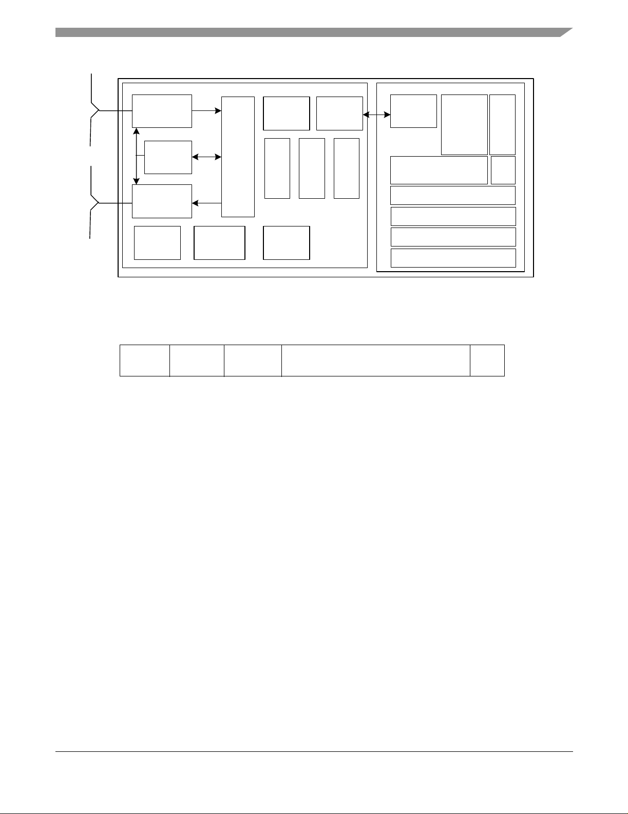
3 Block Diagrams
Figure 3 shows a simplified block diagram of the MC13192/MC13193 which is an IEEE Standard
802.15.4 compatible transceiver that provides the functions required in the physical layer (PHY)
specification. Figure 4 shows the basic system block diagram for the MC13192/MC13193 in an
application. Interface with the transceiver is accomplished through a 4-wire SPI port and interrupt request
line. The media access control (MAC), drivers, and network and application software (as required) reside
on the host processor . The host can vary from a simple 8-bit device up to a sophisticated 32-bit processor
depending on application requirements.
4 Data Transfer Modes
The MC13192/MC13193 has two data transfer modes:
1. Packet Mode — Data is buffered in on-chip RAM
2. Streaming Mode — Data is processed word-by-word
The Freescale 802.15.4 MAC software only supports the streaming mode of data transfer . For proprietary
applications, packet mode can be used to conserve MCU resources.
4.1 Packet Structure
Figure 5 shows the packet structure of the MC13192/MC13193. Payloads of up to 125 bytes are supported.
The MC13192/MC13193 adds a four-byte preamble, a one-byte Start of Frame Delimiter (SFD), and a
one-byte Frame Length Indicator (FLI) before the data. A Frame Check Sequence (FCS) is calculated and
appended to the end of the data.
MC13192/MC13193 Technical Data, Rev. 2.7
Freescale Semiconductor 3
Page 4
Data Transfer Modes
4.2 Receive Path Description
In the receive signal path, the RF input is converted to low IF In-phase and Quadrature (I & Q) signals
through two down-conversion stages. A Clear Channel Assessment (CCA) can be performed based upon
the baseband energy integrated over a specific time interval. The digital back end performs Differential
Chip Detection (DCD), the correlator “de-spreads” the Direct Sequence Spread Spectrum (DSSS) Offset
QPSK (O-QPSK) signal, determines the symbols and packets, and detects the data.
The preamble, SFD, and FLI are parsed and used to detect the payload data and FCS which are stored in
RAM. A two-byte FCS is calculated on the received data and compared to the FCS value appended to the
transmitted data, which generates a Cyclical Redundancy Check (CRC) result. Link Quality is measured
over a 64 µs period after the packet preamble and stored in RAM.
If the MC13192/MC13193 is in packet mode, the data is processed as an entire packet. The MCU is
notified that an entire packet has been received via an interrupt.
If the MC13192/MC13193 is in streaming mode, the MCU is notified by an interrupt on a word-by-word
basis.
Figure 1 shows CCA reported power level versus input power. Note that CCA reported power saturates at
about -57 dBm input power which is well above IEEE 802.15.4 Standard requirements. Figure 2 shows
energy detection/LQI reported level versus input power. Note that for both graphs the required IEEE
802.15.4 Standard accuracy and range limits are shown.
-50
-60
-70
-80
-90
Reported Power Level (dBm)
-100
-90 -80 -70 -60 -50
Input Pow er (dBm)
Figure 1. Reported Power Level versus Input Power in Clear Channel Assessment Mode
802.15.4 Accura cy
and ran ge Re quirements
MC13192/MC13193 Technical Data, Rev. 2.7
4 Freescale Semiconductor
Page 5
-25
-35
-45
-55
Data Transfer Modes
-65
Reported Power Level (dBm)
-75
-85
-85 -75 -65 -55 -45 -35 -25 -15
Input Pow er Level (dBm)
802.1 5.4 Accur acy
and Range Requirements
Figure 2. Reported Power Level Versus Input Power for Energy Detect or Link Quality Indicator
MC13192/MC13193 Technical Data, Rev. 2.7
Freescale Semiconductor 5
Page 6
Data Transfer Modes
4.3 Transmit Path Description
For the transmit path, the TX data that was previously stored in RAM is retrieved (packet mode) or the TX
data is clocked in via the SPI (stream mode), formed into packets per the 802.15.4 PHY, spread, and then
up-converted to the transmit frequency.
If the MC13192/MC13193 is in packet mode, data is processed as an entire packet. The data is first loaded
into the TX buffer. The MCU then requests that the MC13192/MC13193 transmit the data. The MCU is
notified via an interrupt when the whole packet has successfully been transmitted.
In streaming mode, the data is fed to the MC13192/MC13193 on a word-by-word basis with an interrupt
serving as a notification that the MC13192/MC13193 is ready for more data. This continues until the
whole packet is transmitted.
RFIN+
RFIN-
VDDLO2
XTAL1
XTAL2
VDDLO1
PAO+
PAO-
1st IF Mix er
IF = 65 M Hz
LNA
256 MHz
Crystal
Osc illator
16 MHz
PA
2nd IF Mixer
IF = 1 M Hz
÷4
Phase Shift Modulator
PMA
Decima tion
Filter
AGC
Sy n the sizer
Baseband
Mixer
2.45 GHz
VCO
Matched
Filter
Programmable
Prescaler
MUX
CCA
Transmit
Packet RAM 2
Transmit
Packet RAM 1
FCS
Generation
DCD
Receive
Packet RAM
24 Bit Ev ent Timer
4 Programmable
Timer Comparators
Transmit RAM
Arbiter
Header
Generation
Packet
Process or
Symbol
Correlator
Synch & Det
Receive RAM
Arbiter
Sym bol
Generation
Figure 3. MC13192 Simplified Block Diagram
Pow er-U p
Control
Logic
Sequence
Manager
(Control Logic)
Analog
Regulator VBATT
Digital
Regulator L
Digital
Regulator H
Crystal
Regulator
VCO
Regulator
SERIAL
PERIPHERAL
IRQ
Arbiter
INTERFACE
VDDINT
VDDD
VDDVCO
(SPI)
VDDA
RXTXEN
CE
MOSI
MISO
SPICLK
ATTN
RST
GPIO1
GPIO2
GPIO3
GPIO4
GPIO5
GPIO6
GPIO7
IRQ
CLKO
MC13192/MC13193 Technical Data, Rev. 2.7
6 Freescale Semiconductor
Page 7
Data Transfer Modes
MC13192/MC13193
Analog Receiver
Frequency
Generation
Analog
Transmitter
Voltage
Regulators
Power Up
Management
Control
Logic
Digital Transceiver
IRQ Arbiter
Buffer RAM
SPI
and GPIO
Timer
RAM Arbiter
Microcontroller
SPI
CPU A/D
ROM
(Flash)
RAM
Application
Network
MAC
PHY Driver
Figure 4. System Level Block Diagram
4 bytes 1 byte 1 byte 125 bytes maximum 2 bytes
Preamble SFD FLI Payload Data FCS
Timer
Figure 5. MC13192/MC13193 Packet Structure
MC13192/MC13193 Technical Data, Rev. 2.7
Freescale Semiconductor 7
Page 8

Electrical Characteristics
5 Electrical Characteristics
5.1 Maximum Ratings
Table 1. Maximum Ratings
Rating Symbol Value Unit
Power Supply Voltage V
BATT, VDDINT
RF Input Power P
Junction Temperature T
Storage Temperature Rang e T
max
J
stg
3.6 Vdc
TBD dBm
125 °C
-55 to 125 °C
Note: Maximum Ratings are those values beyond which damage to the device may occur.
Functional operation should be restricted to the limits in the Electrical Characteristics
or Recommended Operating Conditions tables.
Note: Meets Human Body Model (HBM) = 2 kV and Machine Model (MM) = 200 V except RFIN± = 100 V MM,
PAO± = 50 V MM & 1 kV HBM, and VBATT = 100 V MM. RF output pins have no ESD protection.
5.2 Recommended Operating Conditions
Table 2. Recommended Operating Conditions
Characteristic Symbol Min Typ Max Unit
Power Supply Voltage (V
Input Frequency f
Ambient Temperature Range T
Logic Input Voltage Low V
Logic Input Voltage High V
SPI Clock Rate f
RF Input Power P
Crystal Reference Oscillator Frequency (±40 ppm over
operating conditions to meet the 802.15.4 standard.)
BATT
= V
)V
DDINT
BATT,
V
DDINT
in
SPI
max
f
ref
A
IL
IH
2.0 2.7 3.4 Vdc
2.405 - 2.480 GHz
-40 25 85 °C
0-30%
V
70%
V
DDINT
-V
--8.0MHz
--10dBm
16 MHz Only
DDINT
DDINT
V
V
MC13192/MC13193 Technical Data, Rev. 2.7
8 Freescale Semiconductor
Page 9

5.3 DC Electrical Characteristics
Table 3. DC Electrical Characteristics
(V
, V
BATT
Characteristic Symbol Min Typ Max Unit
= 2.7 V, TA = 25 °C, unless otherwise noted)
DDINT
Electrical Characteristics
Power Supply Current (V
Off
Hibernate
BATT
+ V
DDINT
)
Doze (No CLKO)
Idle
Transmit Mode
Receive Mode
Input Current (V
= 0 V or V
IN
) (All digital inputs) I
DDINT
Input Low Voltage (All digital inputs) V
Input High Voltage (all digital inputs) V
Output High Voltage (I
= -1 mA) (All digital outputs) V
OH
Output Low Voltage (IOL = 1 mA) (All digital outputs) V
5.4 AC Electrical Characteristics
Table 4. Receiver AC Electrical Characteristics
(V
BATT
, V
= 2.7 V, TA = 25 °C, f
DDINT
I
leakage
I
CCH
I
CCD
I
CCI
I
CCT
I
CCR
IN
IL
IH
OH
OL
= 16 MHz, unless otherwise noted)
ref
-
-
-
-
-
-
--±1µA
0-30%
70%
V
DDINT
80%
V
DDINT
0-20%
0.2
2.3
35
500
30
37
1.0
-
-
800
35
42
V
DDINT
-V
-V
DDINT
DDINT
V
DDINT
µA
µA
µA
µA
mA
mA
V
V
V
V
Characteristic Symbol Min Typ Max Unit
Sensitivity for 1% Packet Error Rate (PER) (-40 to +85 °C) SENS
per
--92-dBm
Sensitivity for 1% Packet Error Rate (PER) (+25 °C) - -92 -87 dBm
Saturation (maximum input level) SENS
Adjacent Channel Interference for 1% PER
max
010 dBm
023-dB
(desired signal -82 dBm)
Alternate Channel Interference for 1% PER
035-dB
(desired signal -82 dBm)
Frequency Error Tolerance (total) ± 100 ± 175 - kHz
Symbol Rate Error Tolerance ± 40 ± 70 - ppm
MC13192/MC13193 Technical Data, Rev. 2.7
Freescale Semiconductor 9
Page 10

Electrical Characteristics
Table 5. Transmitter AC Electrical Characteristics
(V
, V
BATT
Characteristic Symbol Min Typ Max Unit
Power Spectral Density (-40 to +85 °C) Absolute limit - -47 -30 dBm
Power Spectral Density (-40 to +85 °C) Relative limit 20 40 -
= 2.7 V, TA = 25 °C, f
DDINT
= 16 MHz, unless otherwise noted)
ref
Nominal Output Power
P
out
-3 0 3 dBm
(2405-2480 MHz with Register 12 set to {[default],BC})
Error Vector Magnitude EVM - 20 35 %
Power Control Range (10dB steps) - 20 - dB
Over the Air Data Rate - 250 - kbps
Spurious Emissions - -56 -40 dBm
2nd Harmonic - -42 - dBc
3rd Harmonic - -44 - dBc
MC13192/MC13193 Technical Data, Rev. 2.7
10 Freescale Semiconductor
Page 11

Functional Description
6 Functional Description
6.1 MC13192/MC13193 Operational Modes
The MC13192/MC13193 has a number of operational modes that allow for low-current operation.
Transition from the Off to Idle mode occurs when RST is negated. Once in Idle, the SPI is active and is
used to control the IC. Transition to Hibernate and Doze modes is enabled via the SPI. These modes are
summarized, along with the transition times, in Table 6. Current drain in the various modes is listed in
Table 3, DC Electrical Characteristics.
Table 6. MC13192/MC13193 Mode Definitions and Transition Times
Mode Definition
Off All IC functions Off, Leakage only. RST asserted. Digital outputs are
tri-stated including IRQ
Hibernate Crystal Reference Oscillator Off. (SPI not functional.) IC Responds to
ATTN. Data is retained.
Doze Crystal Reference Oscillator On but CLKO output available only if Register
7, Bit 9 = 1 for frequencies of 1 MHz or less. (SPI not functional.) Responds
to ATTN
timer comparator.
Idle Crystal Reference Oscillator On with CLKO output available. SPI active.
Receive Crystal Reference Oscillator On. Receiver On. 144 µs from Idle
Transmit Crystal Reference Oscillator On. Transmitter On. 144 µs from Idle
and can be programmed to enter Idle Mode through an internal
Transition Time
To or From Idle
25 ms to Idle
20 ms to Idle
(300 + 1/CLKO) µs
to Idle
6.2 Serial Peripheral Interface (SPI)
The host microcontroller directs the MC13192/MC13193, checks its status, and reads/writes data to the
device through the 4-wire SPI port. The transceiver operates as a SPI slave device only. A transaction
between the host and the MC13192/MC13193 occurs as multiple 8-bit bursts on the SPI. The SPI signals
are:
1. Chip Enable (CE
) - A transaction on the SPI port is framed by the active low CE input signal. A
transaction is a minimum of 3 SPI bursts and can extend to a greater number of bursts.
2. SPI Clock (SPICLK) - The host drives the SPICLK input to the MC13192/MC13193. Data is
clocked into the master or slave on the leading (rising) edge of the return-to-zero SPICLK and
data out changes state on the trailing (falling) edge of SPICLK.
NOTE
For Freescale microcontrollers, the SPI clock format is the clock phase
control bit CPHA = 0 and the clock polarity control bit CPOL = 0.
3. Master Out/Slave In (MOSI) - Incoming data from the host is presented on the MOSI input.
MC13192/MC13193 Technical Data, Rev. 2.7
Freescale Semiconductor 11
Page 12

Functional Description
4. Master In/Slave Out (MISO) - The MC13192/MC13193 presents data to the master on the MISO
output.
A typical interconnection to a microcontroller is shown in Figure 6.
MCU MC13192/MC13193
Shift Register
Baud Rate
Generator
RxD
TxD MOSI
Sclk SPICLK
Chip Enable (CE)
Figure 6. SPI Interface
MISO
Shift Register
CE
Although the SPI port is fully static, internal memory , timer and interrupt arbiters require an internal clock
(CLK
), derived from the crystal reference oscillator, to communicate from the SPI regis ters to internal
core
registers and memory.
6.2.1 SPI Burst Operation
The SPI port of an MCU transfers data in bursts of 8 bits with most significant bit (MSB) first. The master
(MCU) can send a byte to the slave (transceiver) on the MOSI line and the slave can send a byte to the
master on the MISO line. Although an MC13192/MC13193 transaction is three or more SPI bursts long,
the timing of a single SPI burst is shown in Figure 7.
SPI Burst
CE
1 2345678
SPICLK
T5
T4
V alid
T6
T3
T2
T1
T0
T7
MISO
MOSI
12 Freescale Semiconductor
Valid
Valid
Figure 7. SPI Single Burst Timing Diagram
MC13192/MC13193 Technical Data, Rev. 2.7
Page 13

Functional Description
Table 7. SPI Timing Specifications
Symbol Parameter Min Typ Max Unit
T0 SPICLK period 125 ns
T1 Pulse width, SPICLK low 62.5 ns
T2 Pulse width, SPICLK high 62.5 ns
T3 Delay time, MISO data valid from falling
SPICLK
T4 Setup time, CE low to rising SPICLK 15 ns
T5 Delay time, MISO valid from CE low 15 ns
T6 Setup time, MOSI valid to rising SPICLK 15 ns
T7 Hold time, MOSI valid from rising SPICLK 15 ns
15 ns
6.2.2 SPI Transaction Operation
Although the SPI port of an MCU transfers data in bursts of 8 bits, the MC13192/MC13193 requires that
a complete SPI transaction be framed by CE, and there will be three (3) or more bursts per transaction. The
assertion of CE to low signals the start of a transaction. The first SPI burst is a write of an 8-bit header to
the transceiver (MOSI is valid) that defines a 6-bit address of the internal resource being accessed and
identifies the access as being a read or write operation. In this context, a write is data written to the
MC13192/MC13193 and a read is data written to the SPI master. The following SPI bursts will be either
the write data (MOSI is valid) to the transceiver or read data from the transceiver (MISO is valid).
Although the SPI bus is capable of sending data simultaneously between master and slave, the
MC13192/MC13193 never uses this mode. The number of data bytes (payload) will be a minimum of 2
bytes and can extend to a larger number depending on the type of access. After the final SPI burst, CE is
negated to high to signal the end of the transaction. Refer to the MC13192/MC13193 Reference Manual,
part number MC13192RM/D for more details on SPI registers and transaction types.
An example SPI read transaction with a 2-byte payload is shown in Figure 8.
CE
Clock Burst
SPICLK
MISO
MOSI
Freescale Semiconductor 13
Valid
Header Read data
Figure 8. SPI Read Transaction Diagram
MC13192/MC13193 Technical Data, Rev. 2.7
Valid Valid
Page 14
Pin Connections
7 Pin Connections
Table 8. Pin Function Description
Pin # Pin Name Type Description Functionality
1 RFIN- RF Input LNA negative differential input.
2 RFIN+ RF Input LNA positive differential input.
3 Not Used Tie to Ground.
4 Not Used Tie to Ground.
5 PAO+ RF Output /DC Input Power Amplifier Positive Output. Open
drain. Connect to V
6 PAO- RF Output/DC Input Power Amplifier Negative Output. Open
drain. Connect to V
7 Not used Tie to Ground.
8 GPIO4 Digital Input/ Output General Purpose Input/Output 4.
9 GPIO3 Digital Input/ Output General Purpose Input/Output 3.
10 GPIO2 Digital Input/ Output General Purpose Input/Output 2. When
gpio_alt_en, Register 9, Bit 7 = 1, GPIO2
functions as a “CRC Valid” indicator.
DDA
DDA
.
.
11 GPIO1 Digital Input/ Output General Purpose Input/Output 1. When
gpio_alt_en, Register 9, Bit 7 = 1, GPIO1
functions as an “Out of Idle” indicator.
12 RST Digital Input Active Low Reset. While held low, the IC
is in Off Mode and all internal information
is lost from RAM and SPI registers.
When high, IC goes to IDLE Mode, with
SPI in default state.
13 RXTXEN Digital Input Active High. Low to high transition
initiates RX or TX sequence depending
on SPI setting. If held high (e.g., tied to
VDDINT), SPI programming starts RX or
TX sequence. When held low, forces Idle
Mode.
14 ATTN Digital Input Active Low Attention. Transitions IC from
either Hibernate or Doze Modes to Idle.
15 CLKO Digital Output Clock output to host MCU.
Programmable frequencies of:
16 MHz, 8 MHz, 4 MHz, 2 MHz, 1 MHz,
62.5 kHz, 32.786+ kHz (default),
and 16.393+ kHz.
16 SPICLK Digital Clock Inpu t External clock input for the SPI interface.
17 MOSI Digital Input Master Out/Slave In. Dedicated SPI data
input.
18 MISO Digital Output Master In/Slave Out. Dedicated SPI data
output.
MC13192/MC13193 Technical Data, Rev. 2.7
14 Freescale Semiconductor
Page 15

Pin Connections
Table 8. Pin Function Description (continued)
Pin # Pin Name Type Description Functionality
19 CE Digital Input Active Low Chip Enable. Enables SPI
transfers.
20 IRQ Digital Output Active Low Interrupt Request. Open drain device.
Programmable 40 kΩ internal
pull-up.
Interrupt can be serviced every
6 µs with <20 pF load.
Optional external pull-up must
Ω.
be >4 k
21 VDDD Power Output Digital regulated supply bypass. Decouple to ground.
22 VDDINT Power Input Digital interface supply & digital regulator
input. Connect to Battery.
2.0 to 3.4 V. Decouple to
ground.
23 GPIO5 Digital Input/Output General Purpose Input/Output 5.
24 GPIO6 Digital Input/Output General Purpose Input/Output 6.
25 GPIO7 Digital Input/Output General Purpose Input/Output 7.
26 XTAL1 Input Crystal Reference oscillator input. Connect to 16 MHz crystal and
load capacitor.
27 XTAL2 Input/Output Crystal Reference oscillator output
Note: Do not load this pin by using it as
Connect to 16 MHz crystal and
load capacitor.
a 16 MHz source. Measure 16 MHz
output at Pin 15, CLKO, programmed for
16 MHz. See the MC13192/MC13193
Reference Manual for details.
28 VDDLO2 Power Input LO2 VDD supply. Connect to VDDA
externally.
29 VDDLO1 Power Input LO1 VDD supply. Connect to VDDA
externally.
30 VDDVCO Power Output VCO regulated supply bypass. Decouple to ground.
31 VBATT Power Input Analog voltage regulators Input. Connect
Decouple to ground.
to Battery.
32 VDDA Power Output Analog regulated supply Output.
Decouple to ground.
Connect to directly VDDLO1 and
VDDLO2 externally and to PAO± through
a frequency trap.
EP Ground External paddle / flag ground. Connect to ground.
MC13192/MC13193 Technical Data, Rev. 2.7
Freescale Semiconductor 15
Page 16

Pin Connections
29 28 27 26 25303132
1
2
3
4
5
6
7
8
RFIN-
RFIN+
NC
NC
PAO+
PAONC
GPIO4
VDDA
GPIO3
VBATT
VDDLO1
VDDVCO
EP
VDDLO2
MC13192/
MC13193
RXTXEN
GPIO2
RST
GPIO1
12 13 14 15 1611109
XTAL2
ATTN
XTAL1
VDDINT
CLKO
GPIO7
GPIO6
GPIO5
VDDD
IRQ
CE
MISO
MOSI
SPICLK
24
23
22
21
20
19
18
17
Figure 9. Pin Connections (Top View)
MC13192/MC13193 Technical Data, Rev. 2.7
16 Freescale Semiconductor
Page 17

Applications Information
8 Applications Information
8.1 Crystal Oscillator Reference Frequency
The IEEE 802.15.4 Standard requires that several frequency tolerances be kept within ± 40 ppm accuracy.
This means that a total offset up to 80 ppm between transmitter and receiver will still result in acceptable
performance. The primary determining factor in meeting this specification is the tolerance of the crystal
oscillator reference frequency. A number of factors can contribute to this tolerance and a crystal
specification will quantify each of them:
1. The initial (or make) tolerance of the crystal resonant frequency itself.
2. The variation of the crystal resonant frequency with temperature.
3. The variation of the crystal resonant frequency with time, also commonly known as aging.
4. The variation of the crystal resonant frequency with load capacitance, also commonly known as
pulling. This is affected by:
a) The external load capacitor values - initial tolerance and variation with temperature.
b) The internal trim capacitor values - initial tolerance and variation with temperature.
c) Stray capacitance on the crystal pin nodes - including stray on-chip capacitance, stray package
capacitance and stray board capacitance; and its initial tolerance and variation with
temperature.
Freescale has specified that a 16 MHz crystal with a <9 pF load capacitance is required. The
MC13192/MC13193 does not contain a reference divider, so 16 MHz is the only frequency that can be
used. A crystal requiring higher load capacitance is prohibited because a higher load on the amplifier
circuit may compromise its performance. The crystal manufacturer defines the load capacitance as that
total external capacitance seen across the two terminals of the crystal. The oscillator amplifier
configuration used in the MC13192/MC13193 requires two balanced load capacitors from each terminal
of the crystal to ground. As such, the capacitors are seen to be in series by the crystal, so each must be
<18 pF for proper loading.
In the reference schematic, the external load capacitors are shown as 6.8 pF each, used in conjunction with
a crystal that requires an 8 pF load capacitance. The default internal trim capacitor value (2.4 pF) and stray
capacitance total value (6.8 pF) sum up to 9.2 pF giving a total of 16 pF . The value for the stray capacitance
was determined empirically assuming the default internal trim capacitor value and for a specific board
layout. A different board layout may require a different external load capacitor value. The on-chip trim
capability may be used to determine the closest standard value by adjusting the trim value via the SPI and
observing the frequency at CLKO. Each internal trim load capacitor has a trim range of approximately
± 2.5 pF in 20 µF steps.
Initial tolerance for the internal trim capacitance is approximately ±15%.
Since the MC13192/MC13193 contains an on-chip reference frequency trim capability, it is possible to
trim out virtually all of the initial tolerance factors and put the frequency within 0.12 ppm on a
board-by-board basis.
MC13192/MC13193 Technical Data, Rev. 2.7
Freescale Semiconductor 17
Page 18

Applications Information
A tolerance analysis budget may be created using all the previously stated factors. It is an engineering
judgment whether the worst case tolerance will assume that all factors will vary in the same direction or if
the various factors can be statistically rationalized using RSS (Root-Sum-Square) analysis. The aging
factor is usually specified in ppm/year and the product designer can determine how many years are to be
assumed for the product lifetime. T aking all of the factors into account, the product designer can determine
the needed specifications for the crystal and external load capacitors to meet the IEEE 802.15.4
specification.
8.2 Design Example
Figure 10 shows a basic application schematic for interfacing the MC13192/MC13193 with an MCU.
Table 9 lists the Bill of Materials (BOM).
The MC13192/MC13193 has differential RF inputs and outputs that are well suited to balanced printed
wire antenna structures. Alternatively , as in the application circuit, a printed wire antenna, a chip antenna,
or other single-ended structures can be used with commercially available chip baluns or microstrip
equivalents. PAO+ and PAO- require connection to VDDA, the analog regulator output. This is
accomplished through the baluns in the referenced design.
The 16 MHz crystal should be mounted close to the MC13192/MC13193 because the crystal trim default
assumes that the listed KDS Daishinku crystal (see Table 10) and the 6.8 pF load capacitors shown are
used. If a different crystal is used, it should have a specified load capacitance (stray capacitance, etc.) of
9 pF or less. Bypassing capacitors are critical and should be placed close to the device. Unused pins should
be grounded as shown.
The SPI connections to the MCU include CE, MOSI, MISO, and SPICLK. The SPI can run at a frequency
of 8 MHz or less. Optionally, CLKO can provide a clock to the MCU. The CLKO frequency is
programmable via the SPI and has a default of 32.786+ kHz (16 MHz / 488). The ATTN line can be driven
by a GPIO from the MCU (as shown) or can also be controlled by a switch or other hardware. The latter
approach allows the MCU to be put into a sleep mode and then awakened by CLKO when the ATTN line
wakes up the MC13192/MC13193. RXTXEN can be used to initiate receive or transmit sequences under
MCU control. In this case, RXTXEN must be controlled by an MCU GPIO with the connection shown.
Otherwise, RXTXEN is held high and receive or transmit sequences are initiated by an SPI command.
Device reset (RST) is controlled through a connection to an MCU GPIO.
When the MC13192/MC13193 is used in Stream Mode, as with 802.15.4 MAC/PHY software, the
MC13192/MC13193 GPIO1 functions as an “Out of Idle” indicator and GPIO2 functions as a “CRC
Valid”, Clear Channel Assessment (CCA) result indicator and are not available for general purpose use.
MC13192/MC13193 Technical Data, Rev. 2.7
18 Freescale Semiconductor
Page 19

ANT1
F_Antenna
Applications Information
J1
1
253
4
R2 0
C11
654
VDD
OUT2
IC2
132
C9
10pF
50_Ohm3
50_Ohm4
50_Ohm1
516
Z1
234
L1
6.8nH
LDB212G4020C-001
C7
10pF
50_Ohm6
IN
OUT1
10pF
VCONT
GND
R3
0
C12
0.5pF
L3
8.2nH
µPG 2012TK-E2
C10
10pF
516
Z2
234
VDDA
L2
50_Ohm2
8.2nH
50_Ohm7
LDB212G4020C-001
C8
10pF
C5
6.8pF
SMA Receptacle, Female
C6
6.8pF
IC1
100_Ohm1
1
RIN_M
GPIO1
GPIO2
GPIO3
9
11
10
GPIO4
8
GPIO5
GPIO6
2523242018
100_Ohm2
2
GPIO7
RIN_P
CEB
19
SS
MISO
MISO
17
MOSI
MOSI
16
SCLK
3
Not Used
SPICLK
IRQ
IRQB
4
3V0_BB
R1 470K
Not Used
GPIO
GPIO
14
GPIO
100_Ohm3
5
RXTXEN
ATTNB
12
13
GPIO
GPIO
PAO_P
RSTB
GPIO
15
CLK
100_Ohm4
6
CLKO
MCU
PAO_M
3V0_RF
VBATT
31
7
Not Used
VDDINT
3221222928
VDDA
VDDA
VDDLO1
X1
26
VDDD
VDDLO2
30
XTAL1
VDDVCO
16.000MHz
27
XTAL2
GND
MC13192
EP
C4
220nF
C3
220nF
C2
220nF
C1
1µF
Figure 10. MC13192/MC13193 Configured With an MCU
MC13192/MC13193 Technical Data, Rev. 2.7
Freescale Semiconductor 19
Page 20

Applications Information
Item Quantity Reference Part Manufacturer
1 1 ANT1 F_Antenna Printed wire
21 C1 1 µF
3 3 C2, C3, C4 220 nF
4 2 C5, C6 6.8 pF
Table 9. MC13192/MC13193 to MCU Bill of Materials (BOM)
5 5 C7, C8, C9, C10,
C11
6 1 C12 0.5 pF
7 1 IC1 MC13192/MC13193 Freescale Semiconductor
81 IC2 µPG2012TK-E2 NEC
9 1 J1 SMA Receptacle,
10 1 L1 6.8 nH
1 1 2 L2, L3 8.2 nH
12 1 R1 470 kΩ
13 2 R2, R3 0 Ω
14 1 X1 16.000 MHz, Type
15 2 Z1, Z2 LDB212G4020C-001 Murata
10 pF
Female
KDS, Daishinku Corp
DSX321G, ZD00882
Table 10. Daishinku, KDS - DSX321G, ZD00882 Crystal Specifications
Parameter Value Unit Condition
Type DSX321G surface mount
Frequency 16 MHz
Frequency tolerance ± 20 ppm at 25 °C ± 3 °C
Equivalent series resistance 100 Ω max
Temperature drift ± 20 ppm -10 °C to +60 °C
Load capacitance 8.0 pF
Drive level 10 µW± 2 µW
Shunt capacitance 2 pF max
Mode of oscillation fundamental
MC13192/MC13193 Technical Data, Rev. 2.7
20 Freescale Semiconductor
Page 21

9 Packaging Information
PIN 1
INDEX AREA
2X
32
1
8
N
32X
0.1
2X
EXPOSED DIE
ATTACH PAD
0.1 A B
32X
3.25
2.95
A
C
5
B
25
24
C
17
16 9
0.5
0.3
5
0.1 A B
C
3.25
2.95
VIEW M-M
5
(45 )
(1.73)
0.1
DETAIL M
PIN 1 INDEX
0.5
0.30
0.18
0.1
0.05
Packaging Information
C
M
C
C0.1
C0.05
SEATING PLANE
0.217
0.137
(0.1)
5
G
1.00
1.0
0.75
0.8
0.05
0.00
M
NOTES:
1. ALL DIM ENSIONS ARE IN MILLIMETERS.
2. DIMENSIONING AND TOLERANCING PER ASME
Y14.5M, 1994.
3. THE COMPLETE JEDEC DESIGNATOR FOR THIS
PACKAGE IS: HF-PQFP-N.
4. CORNER CHAMFER MAY NOT BE PRESENT.
DIMENSIONS OF OPTIONAL FEATURES ARE FOR
REFERENCE ONLY.
5. COPLANARITY APPLIES TO LEADS, CORNER
LEADS, AND DIE ATTACH PAD.
0.25
28X
M
C
A B
M
C
6. FOR ANVIL SINGULATED QFN PACKAGES,
MAXIMUM DRAFT ANGLE IS 12°.
(0.25)
0.60
0.24
(0.5)
VIEW ROTATED 90° CLOCKWISE
0.217
0.137
PREFERRED BACKSIDE PIN 1 INDEX
(0.25)
DETAIL G
DETAIL S
DETAIL S
0.065
32X
0.015
PREFERRED CORNER CONFIGURATION
BACKSIDE PIN 1 INDEX OPTION
(0.25)
DETAIL N
4
DETAIL M
DETAIL T
0.475
0.425
R
0.60
0.24
DETAIL N
CORNER CONFIGURATION OPTION
4
1.6
1.5
0.25
0.15
DETAIL M
BACKSIDE PIN 1 INDEX OPTION
BACKSIDE
PIN 1 INDEX
DETAIL M
PREFERRED BACKSIDE PIN 1 INDEX
0.39
2X
0.31
DETAIL T
BACKSIDE PIN 1 INDEX OPTION
5
(90 )
0.1
2X
0.0
Figure 11. Outline Dimensions for QFN-32, 5x5 mm
(Case 1311-03, Issue E)
MC13192/MC13193 Technical Data, Rev. 2.7
Freescale Semiconductor 21
Page 22

How to Reach Us:
USA/Europe/Locations Not Listed:
Freescale Semiconductor Literature Distribution
Center
P.O. Box 5405
Denver, Colorado 80217
1-800-521-6274 or 480-768-2130
Japan:
Freescale Semiconductor Japan Ltd.
Technical Information Center
3-20-1, Minami-Azabu, Minato-ku
Tokyo 106-8573, Japan
81-3-3440-3569
Asia/Pacific:
Freescale Semiconductor Hong Kong Ltd.
2 Dai King Street
Tai Po Industrial Estate
Tai Po, N.T., Hong Kong
852-26668334
Home Page:
www.freescale.com
Information in this document is provided solely to enable system and software implementers to use
Freescale Semiconductor products. There are no express or implied copyright licenses granted
hereunder to design or fabricate any integrated circuits or int egrated circuits based on the informa tion
in this document.
Freescale Semiconductor reserves the right to make changes without furt her notice to any product s
herein. Freescale Semiconductor makes no warranty, representation or guarantee regarding the
suitability of its products for any particular purpose, nor does Freescale Semiconductor assume any
liability arising out of the application or use of any product or circuit, and specifically disclaims any
and all liability, including without limitation consequential or incident al damages. “Typical” parameters
that may be provided in Freescale Semiconductor data sheet s and/or specifications can and do vary
in different applications and actual performance may vary over time. All operating parameters,
including “Typicals”, must be vali dated for each customer application by customer’s technical
experts. Freescale Semiconductor does not convey any l icense und er it s paten t rights no r the right s
of others. Freescale Semiconductor products are not designed, intended, or authorized for use as
components in systems intended for surgical implant into the body, or other applications intended to
support or sustain life, or for any other applicatio n in which the failure of the Freescale Semiconductor
product could create a situation where personal injury or death may occur. Should Buyer pur chase
or use Freescale Semiconductor products for any such unintended or unauthorized application,
Buyer shall indemnify and hold Freescale Semiconductor and its officers, employees, subsidiaries,
affiliates, and distributors harmless against all claims, costs, damages, and expenses, and
reasonable attorney fees arising out of, directly or indirectly, any claim of personal injury or death
associated with such unintended or unauthorized use, even if such claim alleges that Freescale
Semiconductor was negligent regarding the design or manufacture of the part.
Learn More: For more information about Freescale products, please visit www.freescale.com.
Freescale™ and the Freescale logo are trademarks of Freescale Semiconductor, Inc. All other
product or service names are the property of their respective owners.
© Freescale Semiconductor, Inc. 2004. All rights reserved.
MC13192/D
Rev. 2.7
12/2004
 Loading...