

Page 1
Freescale Semiconductor, Inc.
M68HC12A4EVBUM/D
October 1999
..
.
nc
M68HC12A4EVB
T
O
R
,
A
R
EVALUATION BOARD
USER’S MANUAL
M
E SE
L
A
C
S
E
E
R
F
Y
B
D
E
V
I
H
C
C
U
D
N
O
C
I
.
C
N
I
Freescale Semiconductor, I
For More Information On This Product,
Go to: www.freescale.com
Page 2

Freescale Semiconductor, Inc.
Important Notice to Users
..
.
nc
While every effort has been made to ensure the accuracy of all information in
this document, Motorola assumes no liability to any party for any loss or
damage caused by errors or omissions or by statements of any kind in this
document, its updates, supplements, or special editions, whether such errors are
omissions orstatementsresultingfromnegligence, accident, or any other cause.
M
O
C
I
Motorola further assumes no liability arising out of the application or use of any
information,product, or system described herein: nor any liability for incidental
or consequential damages arising from the use of this document. Motorola
disclaims all warranties regarding the information contained herein, whether
R
E
E
S
expressed, implied, or statutory, including implied warranties of
merchantability or fitness for a particular purpose. Motorola makes no
representation that the interconnection of products in the manner described
herein will not infringe on existing or future patent rights, nor do the
descriptions contained herein imply the granting or license to make, use or sell
H
C
equipment constructed in accordance with this description.
R
A
Trademarks
D
E
V
I
This document includes these trademarks:
Motorola and the Motorola logo are registered trademarks
of Motorola, Inc.
MCUez is a trademark of Motorola, Inc.
F
Y
B
C
A
E SE
L
N
D
U
C
T
O
R
,
.
C
N
I
Freescale Semiconductor, I
© Motorola, Inc., 1999; All Rights Reserved
Apple, Macintosh, MacTerminal, and System 7 are registered
trademarks of Apple Computer, Inc.
Windows and Windows 95 are registered trademarks of Microsoft
Corporation in the U.S. and other countries.
Intel is a registered trademark of Intel Corporation.
Motorola, Inc., is an Equal Opportunity / Affirmative Action Employer.
For More Information On This Product,
Go to: www.freescale.com
Page 3

..
.
nc
Freescale Semiconductor, Inc.
User’s Manual — M68HC12A4EVB Evaluation Board
Section 1. General Information . . . . . . . . . . . . . . . . . . . .15
Section 2. Configuration and Setup . . . . . . . . . . . . . . . .27
Section 3. Operation . . . . . . . . . . . . . . . . . . . . . . . . . . . . .37
Section 4. Hardware Reference . . . . . . . . . . . . . . . . . . . .77
R
E
E
S
Appendix A. S-Record Format . . . . . . . . . . . . . . . . . . . .117
F
Appendix B. Communications Program Examples . . .123
D
E
Appendix C. D-Bug12 Startup Code . . . . . . . . . . . . . . .131
V
I
H
C
R
Appendix D. D-Bug12 Customization Data. . . . . . . . . .135
A
Y
B
C
A
E SE
L
M
C
I
O
N
D
U
Appendix E. Customizing the EPROMs . . . . . . . . . . . .141
Appendix F. SDI Configuration . . . . . . . . . . . . . . . . . . .143
Glossary. . . . . . . . . . . . . . . . . . . . . . . . . . . . . . . . . . . . . .145
Index. . . . . . . . . . . . . . . . . . . . . . . . . . . . . . . . . . . . . . . . .149
List of Sections
.
C
N
I
,
R
O
T
C
Freescale Semiconductor, I
M68HC12A4EVB Evaluation Board — Rev. 1 User’s Manual
MOTOROLA List of Sections 3
For More Information On This Product,
Go to: www.freescale.com
Page 4

List of Sections
..
.
nc
A
R
Freescale Semiconductor, Inc.
E
V
I
H
C
D
O
C
I
M
E SE
L
A
C
S
E
E
R
F
Y
B
N
D
U
C
T
O
R
,
.
C
N
I
Freescale Semiconductor, I
User’s Manual M68HC12A4EVB Evaluation Board — Rev. 1
4 List of Sections MOTOROLA
For More Information On This Product,
Go to: www.freescale.com
Page 5

..
.
nc
Freescale Semiconductor, Inc.
User’s Manual — M68HC12A4EVB Evaluation Board
Section 1. General Information
1.1 Contents . . . . . . . . . . . . . . . . . . . . . . . . . . . . . . . . . . . . . . . . . . . . . . . 15
U
C
O
N
D
1.2 Introduction. . . . . . . . . . . . . . . . . . . . . . . . . . . . . . . . . . . . . . . . . . . . . 15
I
1.3 General Description and Features. . . . . . . . . . . . . . . . . . . . . . . . . . . . 15
1.4 Performance Notes . . . . . . . . . . . . . . . . . . . . . . . . . . . . . . . . . . . . . . . 19
1.5 Functional Overview. . . . . . . . . . . . . . . . . . . . . . . . . . . . . . . . . . . . . . 20
1.6 External Equipment Requirements. . . . . . . . . . . . . . . . . . . . . . . . . . . 22
E
1.7 EVB Specifications. . . . . . . . . . . . . . . . . . . . . . . . . . . . . . . . . . . . . . . 23
V
I
H
C
1.8 Typographic Conventions. . . . . . . . . . . . . . . . . . . . . . . . . . . . . . . . . . 24
R
A
1.9 Customer Support . . . . . . . . . . . . . . . . . . . . . . . . . . . . . . . . . . . . . . . . 25
D
Y
B
E
E
R
F
S
C
A
L
M
E SE
Section 2. Configuration and Setup
2.1 Contents . . . . . . . . . . . . . . . . . . . . . . . . . . . . . . . . . . . . . . . . . . . . . . . 27
2.2 Unpacking and Preparation. . . . . . . . . . . . . . . . . . . . . . . . . . . . . . . . . 27
2.3 EVB Configuration. . . . . . . . . . . . . . . . . . . . . . . . . . . . . . . . . . . . . . . 28
Table of Contents
.
C
N
I
,
R
O
T
C
Freescale Semiconductor, I
M68HC12A4EVB Evaluation Board — Rev. 1 User’s Manual
MOTOROLA Table of Contents 5
2.4 EVB to Power Supply Connection . . . . . . . . . . . . . . . . . . . . . . . . . . . 29
2.5 EVB to Terminal Connection . . . . . . . . . . . . . . . . . . . . . . . . . . . . . . . 29
2.6 Terminal Communications Setup . . . . . . . . . . . . . . . . . . . . . . . . . . . . 31
2.6.1 Communication Parameters. . . . . . . . . . . . . . . . . . . . . . . . . . . . . . 31
2.6.2 Dumb-Terminal Setup . . . . . . . . . . . . . . . . . . . . . . . . . . . . . . . . . . 31
2.6.3 Host-Computer Setup. . . . . . . . . . . . . . . . . . . . . . . . . . . . . . . . . . . 31
2.6.4 Changing the Baud Rate . . . . . . . . . . . . . . . . . . . . . . . . . . . . . . . . 32
For More Information On This Product,
Go to: www.freescale.com
Page 6

Table of Contents
Freescale Semiconductor, Inc.
2.7 Using Fast External RAM. . . . . . . . . . . . . . . . . . . . . . . . . . . . . . . . . . 32
2.7.1 Selecting and Replacing the RAM Chips . . . . . . . . . . . . . . . . . . . 32
2.7.2 Reprogramming the RAM Chip Select . . . . . . . . . . . . . . . . . . . . . 33
Section 3. Operation
..
.
nc
Freescale Semiconductor, I
3.1 Contents . . . . . . . . . . . . . . . . . . . . . . . . . . . . . . . . . . . . . . . . . . . . . . . 37
3.2 Startup. . . . . . . . . . . . . . . . . . . . . . . . . . . . . . . . . . . . . . . . . . . . . . . . . 38
3.3 Reset . . . . . . . . . . . . . . . . . . . . . . . . . . . . . . . . . . . . . . . . . . . . . . . . . . 39
3.4 Program Abort . . . . . . . . . . . . . . . . . . . . . . . . . . . . . . . . . . . . . . . . . . 40
3.5 Using D-Bug12 Commands . . . . . . . . . . . . . . . . . . . . . . . . . . . . . . . . 40
E SE
S
C
A
L
3.6 D-Bug12 Command Set . . . . . . . . . . . . . . . . . . . . . . . . . . . . . . . . . . . 43
A
R
C
H
ASM Assemble Instructions . . . . . . . . . . . . . . . . . . . . . 44
BAUD Set Baud Rate . . . . . . . . . . . . . . . . . . . . . . . . . . . 48
Y
BF Block Fill. . . . . . . . . . . . . . . . . . . . . . . . . . . . . . . 49
B
D
BR Breakpoint Set . . . . . . . . . . . . . . . . . . . . . . . . . . . 50
E
V
I
BULK Bulk Erase On-Chip EEPROM . . . . . . . . . . . . . . 51
CALL Call Subroutine . . . . . . . . . . . . . . . . . . . . . . . . . . 52
G Go Execute a User Program . . . . . . . . . . . . . . . . 53
GT Go Till . . . . . . . . . . . . . . . . . . . . . . . . . . . . . . . . . 54
HELP Onscreen Help Summary. . . . . . . . . . . . . . . . . . . 55
LOAD Load S-Record File . . . . . . . . . . . . . . . . . . . . . . . 56
MD Memory Display . . . . . . . . . . . . . . . . . . . . . . . . . 57
MDW Display Memory as 16-Bit Word . . . . . . . . . . . . 58
MM Memory Modify. . . . . . . . . . . . . . . . . . . . . . . . . . 59
MMW Modify 16-Bit Memory Word. . . . . . . . . . . . . . . 60
MOVE Move Memory Block. . . . . . . . . . . . . . . . . . . . . . 61
NOBR Remove Breakpoints . . . . . . . . . . . . . . . . . . . . . . 62
RD Register Display. . . . . . . . . . . . . . . . . . . . . . . . . . 63
RM Register Modify. . . . . . . . . . . . . . . . . . . . . . . . . . 64
T Trace . . . . . . . . . . . . . . . . . . . . . . . . . . . . . . . . . . 65
UPLOAD Display Memory in S-Record Format . . . . . . . . . 67
VERF Verify S-Record File Against Memory . . . . . . . . 68
<RegisterName> Modify Register Value . . . . . . . . . . . . . . . . . . . . 70
E
E
R
F
M
O
C
I
N
D
U
C
T
O
R
,
.
C
N
I
3.7 Alternate Execution from EEPROM . . . . . . . . . . . . . . . . . . . . . . . . . 72
User’s Manual M68HC12A4EVB Evaluation Board — Rev. 1
6 Table of Contents MOTOROLA
For More Information On This Product,
Go to: www.freescale.com
Page 7

..
.
nc
Freescale Semiconductor, Inc.
3.8 Off-Board Code Generation . . . . . . . . . . . . . . . . . . . . . . . . . . . . . . . . 73
3.9 Memory Usage . . . . . . . . . . . . . . . . . . . . . . . . . . . . . . . . . . . . . . . . . . 73
3.9.1 Description. . . . . . . . . . . . . . . . . . . . . . . . . . . . . . . . . . . . . . . . . . . 73
3.9.2 Memory Map . . . . . . . . . . . . . . . . . . . . . . . . . . . . . . . . . . . . . . . . . 74
3.10 Operational Limitations . . . . . . . . . . . . . . . . . . . . . . . . . . . . . . . . . . . 75
3.10.1 On-Chip RAM . . . . . . . . . . . . . . . . . . . . . . . . . . . . . . . . . . . . . . . . 75
3.10.2 SCI Port Usage. . . . . . . . . . . . . . . . . . . . . . . . . . . . . . . . . . . . . . . . 75
3.10.3 Dedicated MCU Pins . . . . . . . . . . . . . . . . . . . . . . . . . . . . . . . . . . . 75
3.10.4 Terminal Communications. . . . . . . . . . . . . . . . . . . . . . . . . . . . . . . 76
4.1 Contents . . . . . . . . . . . . . . . . . . . . . . . . . . . . . . . . . . . . . . . . . . . . . . . 77
4.2 Printed Circuit Board (PCB) Description. . . . . . . . . . . . . . . . . . . . . . 78
4.3 Configuration Headers and Jumper Settings. . . . . . . . . . . . . . . . . . . . 78
4.4 Power Input Circuitry . . . . . . . . . . . . . . . . . . . . . . . . . . . . . . . . . . . . . 83
E
V
I
4.5 Terminal Interface. . . . . . . . . . . . . . . . . . . . . . . . . . . . . . . . . . . . . . . . 83
H
C
R
4.6 Microcontroller. . . . . . . . . . . . . . . . . . . . . . . . . . . . . . . . . . . . . . . . . . 84
A
4.7 Memory. . . . . . . . . . . . . . . . . . . . . . . . . . . . . . . . . . . . . . . . . . . . . . . . 86
4.7.1 Memory Types and Sockets. . . . . . . . . . . . . . . . . . . . . . . . . . . . . . 86
4.7.2 Chip Selects . . . . . . . . . . . . . . . . . . . . . . . . . . . . . . . . . . . . . . . . . . 88
4.7.3 Glue Logic . . . . . . . . . . . . . . . . . . . . . . . . . . . . . . . . . . . . . . . . . . . 89
4.8 Clock Circuitry . . . . . . . . . . . . . . . . . . . . . . . . . . . . . . . . . . . . . . . . . . 90
4.9 Phase-Locked Loop (PLL) . . . . . . . . . . . . . . . . . . . . . . . . . . . . . . . . . 90
D
Table of Contents
.
C
N
I
,
R
O
T
C
U
D
N
M
O
C
I
Section 4. Hardware Reference
E SE
L
A
C
S
E
E
R
F
Y
B
Freescale Semiconductor, I
M68HC12A4EVB Evaluation Board — Rev. 1 User’s Manual
MOTOROLA Table of Contents 7
4.10 Reset . . . . . . . . . . . . . . . . . . . . . . . . . . . . . . . . . . . . . . . . . . . . . . . . . . 90
4.11 Low-Voltage Inhibit (LVI). . . . . . . . . . . . . . . . . . . . . . . . . . . . . . . . . 91
4.12 Analog-to-Digital (A/D) Converter . . . . . . . . . . . . . . . . . . . . . . . . . . 91
4.13 Background Debug Mode (BDM) Interface. . . . . . . . . . . . . . . . . . . . 91
4.14 Prototype Area . . . . . . . . . . . . . . . . . . . . . . . . . . . . . . . . . . . . . . . . . . 92
4.15 MCU Connectors . . . . . . . . . . . . . . . . . . . . . . . . . . . . . . . . . . . . . . . . 94
4.16 Schematics . . . . . . . . . . . . . . . . . . . . . . . . . . . . . . . . . . . . . . . . . . . . . 99
For More Information On This Product,
Go to: www.freescale.com
Page 8

Table of Contents
Freescale Semiconductor, Inc.
Appendix A. S-Record Format
A.1 Contents . . . . . . . . . . . . . . . . . . . . . . . . . . . . . . . . . . . . . . . . . . . . . . 117
A.2 Overview. . . . . . . . . . . . . . . . . . . . . . . . . . . . . . . . . . . . . . . . . . . . . . 117
A.3 S-Record Contents . . . . . . . . . . . . . . . . . . . . . . . . . . . . . . . . . . . . . . 117
..
.
nc
Freescale Semiconductor, I
A.4 S-Record Types. . . . . . . . . . . . . . . . . . . . . . . . . . . . . . . . . . . . . . . . . 119
,
C
T
O
R
A.5 S Record Creation. . . . . . . . . . . . . . . . . . . . . . . . . . . . . . . . . . . . . . . 120
O
N
D
U
A.6 S-Record Example . . . . . . . . . . . . . . . . . . . . . . . . . . . . . . . . . . . . . . 120
A.6.1 S0 Header Record . . . . . . . . . . . . . . . . . . . . . . . . . . . . . . . . . . . . 120
A.6.2 First S1 Record. . . . . . . . . . . . . . . . . . . . . . . . . . . . . . . . . . . . . . . 121
A.6.3 S9 Termination Record . . . . . . . . . . . . . . . . . . . . . . . . . . . . . . . . 122
A.6.4 ASCII Characters. . . . . . . . . . . . . . . . . . . . . . . . . . . . . . . . . . . . . 122
S
E
E
B
Y
R
F
Appendix B. Communications Program Examples
V
E
D
B.1 Contents . . . . . . . . . . . . . . . . . . . . . . . . . . . . . . . . . . . . . . . . . . . . . . 123
I
H
B.2 Introduction. . . . . . . . . . . . . . . . . . . . . . . . . . . . . . . . . . . . . . . . . . . . 124
C
R
A
B.3 Procomm for DOS — IBM PC. . . . . . . . . . . . . . . . . . . . . . . . . . . . . 124
B.3.1 Setup. . . . . . . . . . . . . . . . . . . . . . . . . . . . . . . . . . . . . . . . . . . . . . . 124
B.3.2 S-Record Transfers to EVB Memory. . . . . . . . . . . . . . . . . . . . . . 126
B.4 Kermit for DOS — IBM PC . . . . . . . . . . . . . . . . . . . . . . . . . . . . . . . 126
B.4.1 Setup. . . . . . . . . . . . . . . . . . . . . . . . . . . . . . . . . . . . . . . . . . . . . . . 126
B.4.2 S-Record Transfers to EVB Memory. . . . . . . . . . . . . . . . . . . . . . 127
B.5 Kermit — Sun Workstation . . . . . . . . . . . . . . . . . . . . . . . . . . . . . . . 127
B.5.1 Setup. . . . . . . . . . . . . . . . . . . . . . . . . . . . . . . . . . . . . . . . . . . . . . . 127
B.5.2 S-Record Transfers to EVB Memory. . . . . . . . . . . . . . . . . . . . . . 128
C
A
E SE
L
M
C
I
.
C
N
I
B.6 MacTerminal — Apple Macintosh . . . . . . . . . . . . . . . . . . . . . . . . . . 128
B.6.1 Setup. . . . . . . . . . . . . . . . . . . . . . . . . . . . . . . . . . . . . . . . . . . . . . . 128
B.6.2 S-Record Transfers to EVB Memory. . . . . . . . . . . . . . . . . . . . . . 129
B.7 Red Ryder — Apple Macintosh . . . . . . . . . . . . . . . . . . . . . . . . . . . . 130
B.7.1 Setup. . . . . . . . . . . . . . . . . . . . . . . . . . . . . . . . . . . . . . . . . . . . . . . 130
B.7.2 S-Record Transfers to EVB Memory. . . . . . . . . . . . . . . . . . . . . . 130
User’s Manual M68HC12A4EVB Evaluation Board — Rev. 1
8 Table of Contents MOTOROLA
For More Information On This Product,
Go to: www.freescale.com
Page 9

..
.
nc
Freescale Semiconductor, Inc.
Table of Contents
Appendix C. D-Bug12 Startup Code
Appendix D. D-Bug12 Customization Data
D.1 Contents . . . . . . . . . . . . . . . . . . . . . . . . . . . . . . . . . . . . . . . . . . . . . . 135
D.2 Customization Data Area . . . . . . . . . . . . . . . . . . . . . . . . . . . . . . . . . 135
D.2.1 C Format . . . . . . . . . . . . . . . . . . . . . . . . . . . . . . . . . . . . . . . . . . . 136
T
O
R
,
D.2.2 Assembly Format. . . . . . . . . . . . . . . . . . . . . . . . . . . . . . . . . . . . . 136
D.2.3 Initial User CPU Register Values . . . . . . . . . . . . . . . . . . . . . . . . 136
D.2.4 SysClk Field. . . . . . . . . . . . . . . . . . . . . . . . . . . . . . . . . . . . . . . . . 137
D.2.5 IOBase Field . . . . . . . . . . . . . . . . . . . . . . . . . . . . . . . . . . . . . . . . 137
D.2.6 SCIBaudRegVal Field . . . . . . . . . . . . . . . . . . . . . . . . . . . . . . . . . 137
D.2.7 EEBase and EESize Fields. . . . . . . . . . . . . . . . . . . . . . . . . . . . . . 138
D.2.8 EEPROM Erase/Program Delay Function Pointer Field. . . . . . . 138
D.2.9 Auxiliary Command Table Entries . . . . . . . . . . . . . . . . . . . . . . . 138
F
Y
B
Appendix E. Customizing the EPROMs
D
E
V
I
H
C
R
A
S
E
E
R
Appendix F. SDI Configuration
C
A
E SE
L
M
O
C
I
N
D
U
C
.
C
N
I
Glossary
Index
Freescale Semiconductor, I
M68HC12A4EVB Evaluation Board — Rev. 1 User’s Manual
MOTOROLA Table of Contents 9
For More Information On This Product,
Go to: www.freescale.com
Page 10

Table of Contents
..
.
nc
A
R
Freescale Semiconductor, Inc.
E
V
I
H
C
D
O
C
I
M
E SE
L
A
C
S
E
E
R
F
Y
B
N
D
U
C
T
O
R
,
.
C
N
I
Freescale Semiconductor, I
User’s Manual M68HC12A4EVB Evaluation Board — Rev. 1
10 Table of Contents MOTOROLA
For More Information On This Product,
Go to: www.freescale.com
Page 11

..
.
nc
Freescale Semiconductor, Inc.
User’s Manual — M68HC12A4EVB Evaluation Board
Figure Title Page
1-1 EVB Layout and Component Placement . . . . . . . . . . . . . . . . . . . . . . 18
1-2 System Block Diagram. . . . . . . . . . . . . . . . . . . . . . . . . . . . . . . . . . . . 19
C
I
2-1 EVB Power Connector J6. . . . . . . . . . . . . . . . . . . . . . . . . . . . . . . . . . 29
L
A
E
E
S
C
4-1 Memory Sockets Configuration . . . . . . . . . . . . . . . . . . . . . . . . . . . . . 87
4-2 Chip Select Header . . . . . . . . . . . . . . . . . . . . . . . . . . . . . . . . . . . . . . . 88
4-3 RAM/ROM Logic Diagram . . . . . . . . . . . . . . . . . . . . . . . . . . . . . . . . 89
V
E
D
4-4 Prototype Area (Component Side View) . . . . . . . . . . . . . . . . . . . . . . 93
4-5 MCU Connector J8 (Component-Side View). . . . . . . . . . . . . . . . . . . 94
I
H
C
4-6 MCU Connector J9 (Component-Side View). . . . . . . . . . . . . . . . . . . 95
R
A
B
Y
R
F
M
E SE
O
N
D
U
List of Figures
.
C
N
I
,
R
O
T
C
Freescale Semiconductor, I
M68HC12A4EVB Evaluation Board — Rev. 1 User’s Manual
MOTOROLA List of Figures 11
For More Information On This Product,
Go to: www.freescale.com
Page 12

List of Figures
..
.
nc
A
R
Freescale Semiconductor, Inc.
E
V
I
H
C
D
O
C
I
M
E SE
L
A
C
S
E
E
R
F
Y
B
N
D
U
C
T
O
R
,
.
C
N
I
Freescale Semiconductor, I
User’s Manual M68HC12A4EVB Evaluation Board — Rev. 1
12 List of Figures MOTOROLA
For More Information On This Product,
Go to: www.freescale.com
Page 13

..
.
nc
Freescale Semiconductor, I
Freescale Semiconductor, Inc.
User’s Manual — M68HC12A4EVB Evaluation Board
Table Title Page
1-1 EVB Specifications. . . . . . . . . . . . . . . . . . . . . . . . . . . . . . . . . . . . . . . 23
2-1 RS-232C Interface Cabling. . . . . . . . . . . . . . . . . . . . . . . . . . . . . . . . . 30
2-2 Communication Parameters . . . . . . . . . . . . . . . . . . . . . . . . . . . . . . . . 31
E SE
L
A
E
E
S
C
3-1 D-Bug12 Command-Set Summary . . . . . . . . . . . . . . . . . . . . . . . . . . 42
3-2 M68HC11 to CPU12 Instruction Translation. . . . . . . . . . . . . . . . . . . 45
3-3 CPU12 Registers. . . . . . . . . . . . . . . . . . . . . . . . . . . . . . . . . . . . . . . . . 70
V
E
D
3-4 Condition Code Register Bits . . . . . . . . . . . . . . . . . . . . . . . . . . . . . . . 70
3-5 Factory-Configuration Memory Map . . . . . . . . . . . . . . . . . . . . . . . . . 74
I
H
C
R
A
4-1 Jumper-Selectable Functions . . . . . . . . . . . . . . . . . . . . . . . . . . . . . . . 79
4-2 CPU Mode Selection. . . . . . . . . . . . . . . . . . . . . . . . . . . . . . . . . . . . . . 85
4-3 EVB Memories Supplied . . . . . . . . . . . . . . . . . . . . . . . . . . . . . . . . . . 88
4-4 BDM Connector J5 Pin Assignments. . . . . . . . . . . . . . . . . . . . . . . . . 92
4-5 MCU Connector J8 Pin Assignments . . . . . . . . . . . . . . . . . . . . . . . . 96
4-6 MCU Connector J9 Pin Assignments . . . . . . . . . . . . . . . . . . . . . . . . 98
A-1 S-Record Fields. . . . . . . . . . . . . . . . . . . . . . . . . . . . . . . . . . . . . . . . . 118
A-2 S-Record Field Contents. . . . . . . . . . . . . . . . . . . . . . . . . . . . . . . . . . 118
A-3 S-Record Types. . . . . . . . . . . . . . . . . . . . . . . . . . . . . . . . . . . . . . . . . 119
A-4 S0 Header Record . . . . . . . . . . . . . . . . . . . . . . . . . . . . . . . . . . . . . . 120
A-5 S1 Header Record. . . . . . . . . . . . . . . . . . . . . . . . . . . . . . . . . . . . . . . 121
A-6 S9 Header Record. . . . . . . . . . . . . . . . . . . . . . . . . . . . . . . . . . . . . . . 122
B
Y
R
F
M
C
I
O
N
D
U
C
List of Tables
.
C
N
I
,
R
O
T
E-1 Physical EPROM Addresses. . . . . . . . . . . . . . . . . . . . . . . . . . . . . . . 142
F-1 SDI Memory Map. . . . . . . . . . . . . . . . . . . . . . . . . . . . . . . . . . . . . . . 144
M68HC12A4EVB Evaluation Board — Rev. 1 User’s Manual
MOTOROLA List of Tables 13
For More Information On This Product,
Go to: www.freescale.com
Page 14

List of Tables
..
.
nc
A
R
Freescale Semiconductor, Inc.
E
V
I
H
C
D
O
C
I
M
E SE
L
A
C
S
E
E
R
F
Y
B
N
D
U
C
T
O
R
,
.
C
N
I
Freescale Semiconductor, I
User’s Manual M68HC12A4EVB Evaluation Board — Rev. 1
14 List of Tables MOTOROLA
For More Information On This Product,
Go to: www.freescale.com
Page 15

User’s Manual — M68HC12A4EVB Evaluation Board
1.1 Contents
..
.
nc
1.2 Introduction
Freescale Semiconductor, I
Freescale Semiconductor, Inc.
Section 1. General Information
.
C
N
I
,
R
O
D
U
C
T
1.2 Introduction. . . . . . . . . . . . . . . . . . . . . . . . . . . . . . . . . . . . . . . . . . . . . 15
1.3 General Description and Features. . . . . . . . . . . . . . . . . . . . . . . . . . . . 15
1.4 Performance Notes . . . . . . . . . . . . . . . . . . . . . . . . . . . . . . . . . . . . . . . 19
S
C
A
L
1.5 Functional Overview. . . . . . . . . . . . . . . . . . . . . . . . . . . . . . . . . . . . . . 20
1.6 External Equipment Requirements. . . . . . . . . . . . . . . . . . . . . . . . . . . 22
D
Y
B
1.7 EVB Specifications. . . . . . . . . . . . . . . . . . . . . . . . . . . . . . . . . . . . . . . 23
E
1.8 Typographic Conventions. . . . . . . . . . . . . . . . . . . . . . . . . . . . . . . . . . 24
V
I
H
C
R
1.9 Customer Support . . . . . . . . . . . . . . . . . . . . . . . . . . . . . . . . . . . . . . . . 25
A
This user’s manual provides the necessary information for using the
M68HC12A4EVB evaluation board (EVB), an evaluation, debugging, and
code-generation tool for the MC68HC812A4 microcontroller units (MCU).
Reference items, such as schematic diagrams and parts lists, are shipped as part
of the EVB package.
E
E
R
F
M
E SE
N
O
C
I
1.3 General Description and Features
The EVB is an economical tool for designing and debugging code for and
evaluating the operation of the M68HC12 MCU Family. By providing the
essential MCU timing and input/output (I/O) circuitry, the EVB simplifies user
evaluation of prototype hardware and software.
M68HC12A4EVB Evaluation Board — Rev. 1 User’s Manual
MOTOROLA General Information 15
For More Information On This Product,
Go to: www.freescale.com
Page 16

General Information
..
.
nc
Freescale Semiconductor, I
Freescale Semiconductor, Inc.
The board consists of an 8-inch by 8-inch multi-layer printed circuit board
(PCB) that provides the platform for interface and power connections to the
MC68HC812A4 MCU chip, which is installed in a production socket.
Figure 1-1 shows the EVB’s layout and locations of the major components, as
viewed from the component side of the board.
The block diagram in Figure 1-2 depicts the logical relationships and
interconnections within the EVB and with external equipment.
Hardware features of the EVB include:
• Power, ground, and four signal planes
• Single-supply +3- to +5-Vdc power input (J6)
• Two RS-232C interfaces
• Two memory sockets populated with two 32-Kbyte x 8-bit EPROMs
• Two memory sockets populated with two 8-Kbyte x 8-bit SRAMs
E
V
I
H
C
A
R
• Support for up to 1 MByte of program space and 512 Kbytes of data
• 16-MHz crystal-controlled clock oscillator (Y2) in a socket that can
• Headers for jumper selection of hardware options (for full details of the
.
C
N
I
,
R
O
T
C
U
D
N
O
C
I
M
E SE
L
A
C
S
E
E
B
Y
R
F
(U7 and U9A), containing the D-Bug12 monitor program
D
(U4 and U6A)
space using optional memory configurations
accommodate optional 8- or 14-pin oscillator chips (XY2)
jumper settings, refer to Table 4-1):
– Low-voltage inhibit (LVI) (W1)
– RAM (random-access memory) write-protection (W3)
– MCU chip selects for memory devices (W11)
User’s Manual M68HC12A4EVB Evaluation Board — Rev. 1
16 General Information MOTOROLA
– RAM function select (W12 and W13)
– ROM (read-only memory) function select (W22, W24, W29, W32,
W33, and W36)
– MCU mode control (W30, W34, and W42)
– Alternate execution from on-chip EEPROM (W20)
– Serial communications interface (SCI) configuration (W10, W14,
and W21)
For More Information On This Product,
Go to: www.freescale.com
Page 17

..
.
nc
Freescale Semiconductor, Inc.
• Two 2-row x 30-pin header connectors for access to the MCU’s I/O and
• Prototype expansion area for customized interfacing with the MCU
• Low-profile reset (S1) and program-abort (S2) push-button switches
• LVI protection (U1)
• Light-emitting diode (LED) power-on indicator (DS1)
• Test points for ground connections around the board (E1, E2, E3, E12,
• 2-row x 3-pin header (J5) provides a connector for using background
• Phase-locked loop (PLL) biasing circuitry for altering the MCU’s
Firmware features include:
• D-Bug12 monitor/debugger program, resident in external EPROM
E
V
I
H
C
A
R
• Full support for either dumb-terminal or host-computer terminal
• Single-line assembler/disassembler
• File transfer capability from a host computer, allowing off-board code
bus lines (J8 and J9)
E13, and E14)
debug development tools such as the serial debug interface (SDI)
timebase
F
Y
B
D
(erasable programmable read-only memory)
interface
generation
R
E
E
S
C
A
E SE
L
M
General Information
General Description and Features
.
C
N
I
,
R
O
T
C
U
D
N
O
C
I
Freescale Semiconductor, I
M68HC12A4EVB Evaluation Board — Rev. 1 User’s Manual
MOTOROLA General Information 17
For More Information On This Product,
Go to: www.freescale.com
Page 18
General Information
..
.
nc
A
R
Freescale Semiconductor, Inc.
E
V
I
H
C
D
O
C
I
M
E SE
L
A
C
S
E
E
R
F
Y
B
PROTOTYPE AREA
N
D
U
C
T
O
R
,
.
C
N
I
Freescale Semiconductor, I
Figure 1-1. EVB Layout and Component Placement
User’s Manual M68HC12A4EVB Evaluation Board — Rev. 1
18 General Information MOTOROLA
For More Information On This Product,
Go to: www.freescale.com
Page 19
..
.
nc
PROTO-
TYPE
AREA
EXTERNAL CLOCK
J8 / J9
H
C
R
A
S1 RESET
Freescale Semiconductor, Inc.
J7
E
V
I
EXTAL
XTAL
XFC
/6
V
DD
VSS/6
PA [7:0]
PB [7:0]
PC [7:0]
PD [7:0]
PE [7:0]
PF [6:0]
PG [5:0]
PH [7:0]
PJ [7:0]
Y
PAD [7:0]
B
D
, V
V
RH
BKGD
PS [7:0]
PT [7:0]
RESET
RL
F
MC68HC812A4
E
E
R
MCU
ON-CHIP
EEPROM
A
C
S
ON-CHIP
RAM
112 PINS
TOTAL
SCI0
SCI1
E SE
L
BKGD
O
C
EXTAL
I
M
PE0/XIRQ
PA [7:0]
PB [7:0]
PC [7:0]
PD [7:0]
PE [6:0]
PG [5:0]
PE2/RW
PE3/LSTRB
M68HC12A4EVB
RS-232C
TRANSCEIVER
C
U
D
N
S2 – PROGRAM ABORT
GLUE
LOGIC
Figure 1-2. System Block Diagram
,
R
O
T
CLOCK
EXTERNAL
ROM
AND
RAM
General Information
Performance Notes
J3
TERMINAL
.
J2
SPARE
C
N
I
J6
POWER
J5
BDM INTERFACE
Freescale Semiconductor, I
1.4 Performance Notes
The M68HC12A4EVB’s external RAM memory chips, U4 and U6A, were
chosen to emphasize the EVB’s low-voltage and low-power operational
capability over the range of +3.5 to +5.0 Vdc.
However, these parts are not fast enough to operate at the 16-MHz speed of the
factory-supplied clock oscillator. To use them at this external clock speed, the
D-Bug12 startup code programs the MCU’s RAM chip select to insert one wait
state into each access of external RAM. Thus, when programs are run from
M68HC12A4EVB Evaluation Board — Rev. 1 User’s Manual
MOTOROLA General Information 19
For More Information On This Product,
Go to: www.freescale.com
Page 20

General Information
..
.
nc
NOTE:
1.5 Functional Overview
Freescale Semiconductor, I
Freescale Semiconductor, Inc.
external RAM, performance is approximately 40 percent slower than it would
be if the RAM chips were fast enough to run without wait states. Typical
software performance improvements of 80 to 95 percent can be realized with
faster external RAM.
For high-speed performance, the factory-supplied RAM devices may be
replaced with faster parts that allow programs to execute at the full external
clock speed. Two steps are required for this:
1. Replace the RAM devices, U4 and U6A, with faster parts.
2. Modify the RAM chip select to eliminate the wait state (E-clock stretch).
Detailed instructions for these procedures are found in 2.7 Using Fast External
RAM.
Programsthat execute exclusively from theMCU’s on-chip RAM and EEPROM
alwaysrun at the fullclock speed. No wait states are introduced when accessing
these areas.
Table 3-5. Factory-Configuration Memory Map, the default memory map,
E
V
I
depicts the addresses of the EVB’s different memory areas.
H
C
R
A
The EVB is factory-configured to execute D-Bug12, the EPROM-resident
monitor program, without further configuration by the user. It is ready for use
with an RS-232C terminal for writing and debugging user code. Follow the
setup instructions in Section 2. Configuration and Setup to prepare for
operation.
Optionally, the EVB can accommodate various types and configurations of
external memory to suit a particular application’s requirements. These custom
configurations are made by installing the appropriate memory chips in the
EVB’s memory sockets and by setting jumpers on the EVB to correctly
establish the MC68HC812A4’s memory-access operations. Table 1-1 lists the
allowable sizes and types of memory. For the correct jumper settings, refer to
4.3 Configuration Headers and Jumper Settings.
D
.
C
N
I
,
R
O
T
C
U
D
N
O
C
I
M
E SE
L
A
C
S
E
E
R
F
Y
B
NOTE:
User’s Manual M68HC12A4EVB Evaluation Board — Rev. 1
20 General Information MOTOROLA
The D-Bug12 operating instructions in this manual presume the factory-default
memory configuration. Other configurations require different
operating-software arrangements.
For More Information On This Product,
Go to: www.freescale.com
Page 21

..
.
nc
NOTE:
A
Freescale Semiconductor, Inc.
The MC68HC812A4’s two serial communications interface (SCI) ports are
associated with separate RS-232C interfaces. D-Bug12 uses one of the SCIs for
communications with the user terminal (jumper-selectable, SCI0 by default).
The second SCI port is available for user applications. For information on the
ports and their connectors, refer to 2.5 EVB to Terminal Connection and 4.5
Terminal Interface.
If the MCU’s single-wire background debug mode (BDM) interface serves as
the user interface, both of the SCI ports become available for user applications.
This mode requires a background debug development tool, such as Motorola’s
serial debug interface (SDI), and a host computer with the appropriate interface
software. For more information, refer to Appendix F. SDI Configuration and
tothe Serial Debug Interface User’s Manual, Motoroladocument order number
SDIUM/D.
D-Bug12 does not use the BDM interface.
Two methods may be used to generate EVB user code:
E
• For small programs or subroutines, D-Bug12’s single-line
V
I
H
C
R
• For larger programs, the Motorola MCUez assembler may be used on
The EVB features a prototype area, which allows custom interfacing with the
MCU’s I/O and bus lines. These connections are broken out via headers J8 and
J9, which are immediately adjacent to the prototype area as shown in
Figure 1-1.
General Information
Functional Overview
.
C
N
I
,
R
O
T
C
U
D
N
O
C
I
M
E SE
L
A
C
S
E
E
R
F
Y
B
D
assembler/disassembler may be used to place object code directly into
the EVB’s memory.
a host computer to generate S-record object files, which then can be
loaded into the EVB’s memory using D-Bug12’s LOAD command.
Freescale Semiconductor, I
M68HC12A4EVB Evaluation Board — Rev. 1 User’s Manual
MOTOROLA General Information 21
An on-board push-button switch, S1, provides for resetting the EVB hardware
and restarting D-Bug12. Another on-board switch, S2, allows aborting the
execution of a user program, useful in regaining control of a runaway program.
Both of these switch functions are available for customized use in the prototype
area.
The EVB can begin operation in either of two jumper-selectable (W20) modes
at reset. In normal mode, D-Bug12 immediately issues its command prompt on
the terminal display and waits for a user entry. In the alternate mode, execution
For More Information On This Product,
Go to: www.freescale.com
Page 22

General Information
Freescale Semiconductor, Inc.
begins directly with the user code in on-chip EEPROM. This hardware function
is also available for customized use in the prototype area.
D-Bug12 allows programming of the MC68HC812A4’s on-chip EEPROM
through commands that directly alter memory. For full details of all the
commands, refer to 3.6 D-Bug12 Command Set.
Because the MCU must manage the EVB hardware and execute D-Bug12 in
addition to serving as the user-application processor, there are a few restrictions
on its use. For more information, refer to 3.10 Operational Limitations.
1.6 External Equipment Requirements
..
.
nc
NOTE:
Freescale Semiconductor, I
In addition to the EVB, the following user-supplied external equipment is
required:
• Power supply — See Table 1-1 for voltage and current requirements.
Table 1-1 indicates that EVB operation at +3.0 Vdc requires the slower clock
speed of 8 MHz. This limitation applies to programs (including the operating
firmware, D-Bug12) that use external memory.
If an application program uses on-chip RAM and EEPROM exclusively — for
H
C
instance, if external memory is not used — the clock speed can remain at
R
A
16 MHz with a supply voltage of +3.0 Vdc.
D
E
V
I
• User terminal — Options:
Y
B
– RS-232C dumb terminal — Allows single-line on-board code
assembly and disassembly
– Host computer with RS-232C serial port — Allows off-board code
assembly that can be loaded into the EVB’s memory. Requires a
user-supplied communications program capable of emulating a
dumb terminal. Examples of acceptable communications programs
are given in Appendix B. Communications Program Examples.
F
R
E
E
S
C
A
E SE
L
M
.
C
N
I
,
R
O
T
C
U
D
N
O
C
I
• Power-supply and terminal interconnection cables as required
For full details of equipment setup, cabling, and special requirements, refer to
Section 2. Configuration and Setup.
User’s Manual M68HC12A4EVB Evaluation Board — Rev. 1
22 General Information MOTOROLA
– Host computer using the MCU’s BDM (background debug mode)
interface — Frees both of the MCU’s SCI ports for user applications.
Requires a background debug development tool, such as the
Motorola serial debug interface (SDI), and the appropriate interface
software
For More Information On This Product,
Go to: www.freescale.com
Page 23
Freescale Semiconductor, Inc.
1.7 EVB Specifications
Table 1-1 lists the EVB specifications.
General Information
EVB Specifications
Table 1-1. EVB Specifications
..
.
nc
Characteristic Specifications
MCU MC68HC812A4
SRAM maximum memory:
Wide mode
Narrow mode
ROM maximum memory:
EPROM:
Wide mode
Narrow mode
EEPROM:
Wide mode
Narrow mode
MCU I/O ports HCMOS compatible
Background debug mode interface 2-row x 3-pin header
Communications ports Two RS-232C DCE ports
Power requirements:
16-MHz clock source
8-MHz clock source
Prototype area:
Area
Holes
Board dimensions 8 inches x 8 inches
A
R
C
H
E
V
I
16, 64, 256, or 1024 Kbytes
8, 32, 128, or 512 Kbytes
M
C
A
E SE
L
64, 128, 256, 512, or 1024 Kbytes
32, 64, 128, 256, or 512 Kbytes
S
E
E
64, 128, 256, or 512 Kbytes
R
F
32, 64, 128, or 256 Kbytes
Y
B
D
+3.5 to +5.0 Vdc @ 150 mA (max.), fuse-protected @ 1.5 A
+3.0 to +5.0 Vdc @ 150 mA (max.), fuse-protected @ 1.5 A
2 inches x 8 inches, approximately
79 wide x 20 high (0.1-inch centers)
.
C
N
I
,
R
O
T
C
U
D
N
O
C
I
Freescale Semiconductor, I
M68HC12A4EVB Evaluation Board — Rev. 1 User’s Manual
MOTOROLA General Information 23
For More Information On This Product,
Go to: www.freescale.com
Page 24

General Information
1.8 Typographic Conventions
This user’s manual uses special typographical conventions to enhance
readability. They are:
..
.
nc
H
C
R
A
Freescale Semiconductor, I
Freescale Semiconductor, Inc.
• Code, statements, confirmations, data entry, field text, parameters, and
• When arguments in code are italicized, they are placeholders for values
E
V
• In code, the user’s entry is underlined. This underlining does not actually
I
• Window names and parts of windows are indicated in initial caps, unless
strings are indicated in regular Courier:
.
,
C
N
I
$INCLUDE
“INIT.AS”
This option displays an Exit Application confirmation message.
This new filename replaces the [NONAME#1] in the title bar.
%FILE%
E SE
L
A
C
R
E
E
S
to be entered by the user:
<
n
>
F
Y
B
<argument>
D
appear onscreen.
A typical example looks like this:
>
baud 9600 User’s entry
Change Terminal BR, D-Bug12’s response
Press Return
> D-Bug12 prompt for next entry
the name of the window is capitalized in a unique way:
Memory and Code windows
M
C
I
O
N
D
U
C
T
O
R
• For usage in this manual, filenames are not case sensitive. But for
User’s Manual M68HC12A4EVB Evaluation Board — Rev. 1
24 General Information MOTOROLA
CASM08W window
WinIDE main window
consistency, they will always appear in all capital letters:
SETUP.EXE
MAP file
For More Information On This Product,
Go to: www.freescale.com
Page 25

Freescale Semiconductor, Inc.
• Buttons, icons, functions, and keyboard keys are indicated in small caps:
General Information
Customer Support
..
.
nc
1.9 Customer Support
Press the
Type
The
• Commands are not case sensitive. But for consistency, they will always
appear in all capital letters, unless they contain some peculiarity:
INPUTx
UNDO
LOADMAP
• Menu names, options, and tabs, and dialog, edit, text, and lists boxes are
indicated in Times bold:
Do this by checking the Main File option in the Environment
Settings dialog’s General Options tab.
F
Y
Open the Open File dialog.
B
D
E
V
I
H
C
R
A
To obtain information about technical support or ordering parts, call the
Motorola help desk at 800-521-6274.
Select the filename in the File Name list, and use the filename in the
Main filename edit box.
ENTER key.
CTRL + N or click on the NEW toolbar button.
RESET function is an input and output.
I
,
R
O
T
C
U
D
N
O
C
I
M
E SE
L
A
C
S
E
E
R
N
C
.
Freescale Semiconductor, I
M68HC12A4EVB Evaluation Board — Rev. 1 User’s Manual
MOTOROLA General Information 25
For More Information On This Product,
Go to: www.freescale.com
Page 26

General Information
..
.
nc
A
R
Freescale Semiconductor, Inc.
E
V
I
H
C
D
O
C
I
M
E SE
L
A
C
S
E
E
R
F
Y
B
N
D
U
C
T
O
R
,
.
C
N
I
Freescale Semiconductor, I
User’s Manual M68HC12A4EVB Evaluation Board — Rev. 1
26 General Information MOTOROLA
For More Information On This Product,
Go to: www.freescale.com
Page 27

Freescale Semiconductor, Inc.
User’s Manual — M68HC12A4EVB Evaluation Board
2.1 Contents
2.2 Unpacking and Preparation. . . . . . . . . . . . . . . . . . . . . . . . . . . . . . . . . 27
..
.
nc
2.3 EVB Configuration. . . . . . . . . . . . . . . . . . . . . . . . . . . . . . . . . . . . . . . 28
2.4 EVB to Power Supply Connection . . . . . . . . . . . . . . . . . . . . . . . . . . . 29
2.5 EVB to Terminal Connection . . . . . . . . . . . . . . . . . . . . . . . . . . . . . . . 29
2.6 Terminal Communications Setup . . . . . . . . . . . . . . . . . . . . . . . . . . . . 31
2.6.1 Communication Parameters. . . . . . . . . . . . . . . . . . . . . . . . . . . . . . 31
2.6.2 Dumb-Terminal Setup . . . . . . . . . . . . . . . . . . . . . . . . . . . . . . . . . . 31
2.6.3 Host-Computer Setup. . . . . . . . . . . . . . . . . . . . . . . . . . . . . . . . . . . 31
V
I
H
2.6.4 Changing the Baud Rate . . . . . . . . . . . . . . . . . . . . . . . . . . . . . . . . 32
C
R
A
2.7 Using Fast External RAM. . . . . . . . . . . . . . . . . . . . . . . . . . . . . . . . . . 32
2.7.1 Selecting and Replacing the RAM Chips . . . . . . . . . . . . . . . . . . . 32
2.7.2 Reprogramming the RAM Chip Select . . . . . . . . . . . . . . . . . . . . . 33
2.2 Unpacking and Preparation
Before beginning configuration and setup of the EVB:
Freescale Semiconductor, I
1. Verify that these items are present in the EVB package:
Section 2. Configuration and Setup
C
I
M
E SE
L
A
C
S
E
E
R
F
Y
B
D
E
• M68HC12A4EVB board assembly
O
N
D
U
C
T
O
R
,
.
C
N
I
M68HC12A4EVB Evaluation Board — Rev. 1 User’s Manual
MOTOROLA Configuration and Setup 27
• Warranty and registration cards
• EVB schematic diagram and parts list
• M68HC12A4EVB User’s Manual
• MC68HC812A4 Technical Summary
• CPU12 Reference Manual
For More Information On This Product,
Go to: www.freescale.com
Page 28

Freescale Semiconductor, Inc.
Configuration and Setup
• MC68HC12 Family Brochure
• Using D-Bug12 Callable Routines
• Demo software
• Assembly language development toolset
..
.
nc
2.3 EVB Configuration
Freescale Semiconductor, I
2. Remove the EVB from its anti-static shipping bag.
3. Carefully remove the protective case and conductive foam that cover the
MCU and its socket during shipment.
C
U
C
O
N
D
4. Save all packing materials for storing and shipping the EVB.
5. Inspect the alignment of the MCU’s pins within its socket. If it appears
necessary to reseat the MCU:
E SE
L
E
S
C
A
a. Press down on two opposite sides of the MCU socket.
b. Gently press the MCU chip into place.
c. Release the MCU socket.
B
D
E
6. Verify that all other socketed parts are correctly seated.
V
I
H
C
R
A
Becausethe EVB has been factory-configuredto operate withD-Bug12, it is not
necessary to change any of the jumper settings to begin operating immediately.
Only one jumper (header W20) should be changed during the course of
factory-default EVB operation with D-Bug12:
• Pins 2 and 3 jumpered (default) — Normal execution mode. D-Bug12 is
executed from external EPROM upon reset. The D-Bug12 prompt
appears immediately on the terminal display.
Y
E
R
F
M
I
T
O
R
,
.
C
N
I
• Pins 1 and 2 jumpered — Alternate execution mode. User code is
Other jumper settings affect the hardware setup and/or MCU operational
modes. For an overview of all jumper-selectable functions, refer to 1.3 General
Description and Features. For details of the settings, see Table 4-1.
Jumper-Selectable Functions.
User’s Manual M68HC12A4EVB Evaluation Board — Rev. 1
28 Configuration and Setup MOTOROLA
executedfrom on-chip EEPROMupon reset. For more information, refer
to 3.7 Alternate Execution from EEPROM.
For More Information On This Product,
Go to: www.freescale.com
Page 29
Freescale Semiconductor, Inc.
2.4 EVB to Power Supply Connection
The EVB requires a user-provided external power supply. See Table 1-1. EVB
Specifications for the voltage and current specifications. For full details of the
EVB’s power-input circuitry, refer to 4.4 Power Input Circuitry.
Configuration and Setup
EVB to Power Supply Connection
..
.
nc
CAUTION:
A
Although fuse protection is built into the EVB, a power supply with
current-limiting capability is desirable. If this feature is available on the power
T
O
R
,
supply, set it to 200 mA.
N
D
U
C
Connect the external power supply to connector J6 on the EVB as shown in
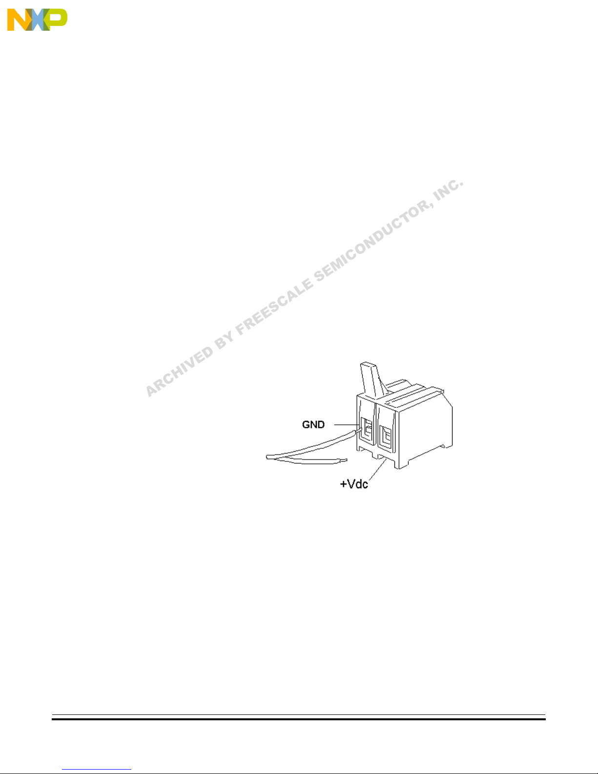
Figure 2-1, using 20 AWG or smaller insulated wire. Strip each wire’s
insulation 1/4 inch from the end, lift the J6 contact lever to release tension on
the contact, insert the bare end of the wire into J6, and close the lever to secure
the wire. Observe the polarity carefully.
S
Do not use wire larger than 20 AWG in connector J6. Larger wire could
damage the connector.
E
V
I
H
C
R
D
Y
B
E
E
R
F
Figure 2-1. EVB Power Connector J6
C
A
E SE
L
M
O
C
I
.
C
N
I
Freescale Semiconductor, I
2.5 EVB to Terminal Connection
For factory-default operation, connect the terminal to J3 or J4 on the EVB, as
shown in Table 2-1. This setup uses the MCU’s SCI port 0 (SCI0) and its
associated RS-232C interface for communications with the terminal device.
To use SCI1 and the second RS-232C interface for the terminal, the EVB’s
hardware setup must be modified. For details, refer to 4.5 Terminal Interface.
M68HC12A4EVB Evaluation Board — Rev. 1 User’s Manual
MOTOROLA Configuration and Setup 29
For More Information On This Product,
Go to: www.freescale.com
Page 30
Configuration and Setup
..
.
nc
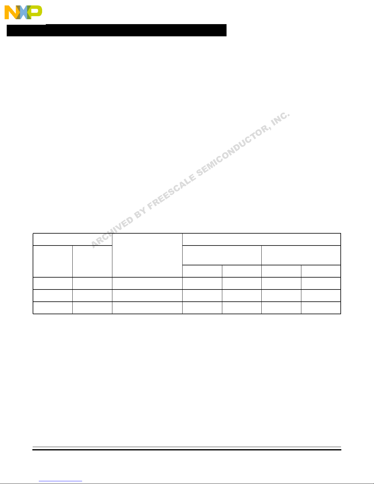
EVB Pins, Always DCE
(1)
J3
Receptacle
(1)
(2)
Freescale Semiconductor, I
(3)
(4)
(2)
/ J2
DB-9
2 2 Receive data (RXD) 2233
3 3 Transmit data (TXD) 3322
5 1 Ground (GND) 5757
Factory default. Terminal interface uses SCI0.
Optional. Terminal interface uses SCI1. Hardware modifications are required. For details, refer to 4.5 Terminal
Interface.
Normal (DCE-to-DTE) cable connections
Null modem (DCE-to-DCE) cable connections
(1)
J4
3-Pin
Header
A
/ J1
Freescale Semiconductor, Inc.
Standard, commercially available cables may be used in most cases. Note that
the EVB uses only three of the RS-232C signals. Table 2-1 lists these signals
and their pin assignments.
The EVB’s RS-232C connectors, J2 (default) and J3 (unpopulated footprint),
are wired as data circuit-terminating equipment (DCE) and employ 9-pin
subminiature D (DB-9) receptacles. The equivalent 3-pin headers, J1 and J4,
serve the same purposes and may be used for customized cabling.
,
R
U
C
T
O
Most terminal devices — whether dumb terminals or the serial ports on host
computers — are wired as data terminal equipment (DTE) and employ 9- or
25-pin subminiature D (DB-9 or DB-25) plugs. In these cases, normal
straight-through cabling is used between the EVB and the terminal. Adapters
M
I
C
O
N
D
.
C
N
I
are readily available for connecting 9-pin cables to 25-pin terminal connectors.
E SE
L
E
S
C
A
Terminal Pins
(3)
DTE
Plug
DB-9 DB-25 DB-9 DB-25
DCE
Receptacle
(4)
If the terminal device is wired as DCE, the RXD and TXD lines must be
cross-connected, as shown in Table 2-1. Commercial null modem adapter
cables are available for this purpose.
B
D
Table 2-1. RS-232C Interface Cabling
E
V
I
H
C
R
(2)
DTE Signal
Y
E
R
F
Optionally, the MCU’s background debug mode (BDM) interface can serve as
the user interface. This setup makes both of the SCI ports available for user
applications. Additional hardware and software are required. For more
information, refer to the documentation for the background debug development
tool being used, such as Motorola’s serial debug interface.
NOTE:
User’s Manual M68HC12A4EVB Evaluation Board — Rev. 1
30 Configuration and Setup MOTOROLA
D-Bug12 does not use the BDM interface.
For More Information On This Product,
Go to: www.freescale.com
Page 31
Freescale Semiconductor, Inc.
2.6 Terminal Communications Setup
This section describes how to set up the terminal communications.
2.6.1 Communication Parameters
The EVB’s serial communications ports use the communication parameters
listedin Table 2-2. Of these, only thebaud rate canbe changed. For instructions
on changing it, refer to 2.6.4 Changing the Baud Rate.
..
.
nc
2.6.2 Dumb-Terminal Setup
2.6.3 Host-Computer Setup
Freescale Semiconductor, I
Configuring a dumb terminal for use with the EVB consists of setting its
V
I
H
parameters as shown in Table 2-2. Many terminals are configurable with
C
R
externally accessible switches, but the procedure differs between brands and
A
models. Consult the manufacturer’s instructions for the terminal being used.
One advantage of using a host computer as the EVB’s terminal is the ability to
generate code off-board, for subsequent loading into the EVB’s memory. It is
thus desirable for the host to be capable of runningprograms such as Motorola’s
MCUez assembler. For more information, see 3.8 Off-Board Code
Generation.
To serve as the EVB’s terminal, the host computer must have an RS-232C serial
port and an installed communications program capable of operating with the
parameters listed in Table 2-2.
E
D
B
Terminal Communications Setup
N
D
U
C
Table 2-2. Communication Parameters
M
O
C
I
Y
Baud Rate 9600
Data Bits 8
E SE
Stop Bits 1
L
A
C
S
E
E
R
F
Parity None
T
Configuration and Setup
.
C
N
I
,
R
O
Setting up the parameters is normally done within the communications
program, after it has been started on the host. Usually, the setup can be saved in
a configuration file so that it does not have to be repeated. Because procedures
vary between programs, consult the user’s guide for the specific program.
Appendix B. Communications Program Examples provides examples of
using some of the commonly available communications programs.
M68HC12A4EVB Evaluation Board — Rev. 1 User’s Manual
MOTOROLA Configuration and Setup 31
For More Information On This Product,
Go to: www.freescale.com
Page 32

Freescale Semiconductor, Inc.
Configuration and Setup
2.6.4 Changing the Baud Rate
The EVB’s default baud rate for the RS-232C ports is 9600. This can be
changed in two ways:
• For temporary changes, use the D-Bug12 BAUD command. This change
remains in effect only until the next reset or power-up, when the baud
rate returns to 9600.
• For permanent changes, the D-Bug12 baud-rate initialization value
stored in EPROM must be modified. For instructions, refer to
..
.
Appendix D. D-Bug12 Customization Data and Appendix E.
Customizing the EPROMs.
nc
2.7 Using Fast External RAM
To replace the two factory-supplied SRAM chips with parts capable of
F
operation at the full 16-MHz external clock speed (8-MHz E-clock) with no
wait states, two operations are required:
H
C
R
A
2.7.1 Selecting and Replacing the RAM Chips
The replacement 8-Kbyte x 8-bit SRAM devices should have a chip-select
access time of less than 60 nanoseconds. An example of a device that has been
used successfully is the Integrated Device Technologies part number
Freescale Semiconductor, I
IDT7164L25P (8 Kbytes x 8 bits, 25 ns).
D
E
V
I
1. Replace the SRAM chips with suitably fast parts. See 2.7.1 Selecting
2. Reprogram the SRAM chip select,
Y
B
and Replacing the RAM Chips.
See 2.7.2 Reprogramming the RAM Chip Select.
R
E
E
S
C
A
E SE
L
M
.
C
N
I
,
R
O
T
C
U
D
N
O
C
I
CSD, for zero-wait-state operation.
When installing the replacement SRAM devices, make sure that their pins align
with the rightmost ends of sockets U4 and U6A, as viewed in Figure 1-1. EVB
Layout and Component Placement.
User’s Manual M68HC12A4EVB Evaluation Board — Rev. 1
32 Configuration and Setup MOTOROLA
For More Information On This Product,
Go to: www.freescale.com
Page 33

Freescale Semiconductor, Inc.
2.7.2 Reprogramming the RAM Chip Select
Configuration and Setup
Using Fast External RAM
..
.
nc
NOTE:
A
NOTE:
Either of two methods may be used to reprogram the RAM chip select,
eliminate the wait state.
Before attempting either of the following methods, ensure that the EVB is
operating properly by following the startup instructions in 3.2 Startup.
Method A — Modifying the CSSTR0 register in memory (temporary)
This method may be used without altering the D-Bug12 startup code in
EPROM. However, it must be repeated each time the EVB is powered up or
M
O
C
I
reset.
Using D-Bug12’s MM (MEMORY MODIFY) command, change the value at
memory location $003E from $05 to $04.
S
E
Y
E
R
F
Method B — Modifying the D-Bug12 startup code in EPROM (permanent)
E
D
B
This method is accomplished by reprogramming a single byte in the
factory-supplied, one-time-programmable (OTP) EPROM, U7. An EPROM
V
I
H
programmer is required.
C
R
Method B does not work in reverse. If U7 has already been reprogrammed
using this technique, it cannot be restored to its original state.
If the EPROMs are to be customized in some other way — for example, to add
a user program or to modify another aspect of D-Bug12 — the change to
registerCSSTR0 can be made in the startupsource code. For more information,
refer to Appendix C. D-Bug12 Startup Code and Appendix E. Customizing
the EPROMs.
C
A
E SE
L
N
D
U
C
T
O
R
,
.
C
N
I
CSD, to
Freescale Semiconductor, I
M68HC12A4EVB Evaluation Board — Rev. 1 User’s Manual
MOTOROLA Configuration and Setup 33
To permanently reprogram U7 for zero RAM wait states, follow these steps:
1. Remove power from the EVB.
2. Being careful not to bend any pins, remove U7 from its socket on the
3. Following the instructions and using the software for the EPROM
EVB and install it in the appropriate socket on the EPROM programmer.
programmer, perform the steps in procedure 1 or procedure 2, as
described here.
For More Information On This Product,
Go to: www.freescale.com
Page 34

Configuration and Setup
Procedure 1 1. Select the Atmel Corporation’s device type AT27LV256R.
..
.
nc
A
Freescale Semiconductor, Inc.
Some EPROM programmers do not have an editable RAM buffer capable of
holding the entire contents of U7. Instead, they program EPROMs directly from
the contents of a disk file.
If the programmer being used has an editable RAM buffer large enough to hold
the contents of U7, use procedure 1. Otherwise, to reprogram U7 from a disk
file, use procedure 2.
2. Read the contents of U7 into the EPROM programmer’s editable RAM
3. Before modifying U7, save a copy of its contents to a disk file for backup
4. Change the contents of the programmer’s editable RAM buffer at
5. Reprogram U7 with the edited contents of the programmer’s RAM
E
V
I
H
6. Reinstall U7 in its socket on the EVB. Be sure that its pins align with the
C
R
7. Apply power to the EVB and press S1, the reset switch. The D-Bug12
8. Ensure that the modification was performed properly by using
.
C
N
I
,
R
O
T
C
U
D
buffer.
M
purposes.
S
E
Y
E
R
F
location $7ED6 from $05 to $04.
B
D
buffer.
rightmost end of its socket, as viewed in Figure 1-1. EVB Layout and
Component Placement.
prompt should appear on the terminal display.
D-Bug12’s MD command to examine the CSSTR0 register at memory
location $003E. It should contain the value $04.
C
A
E SE
L
N
O
C
I
Freescale Semiconductor, I
User’s Manual M68HC12A4EVB Evaluation Board — Rev. 1
34 Configuration and Setup MOTOROLA
For More Information On This Product,
Go to: www.freescale.com
Page 35

..
.
nc
Freescale Semiconductor, Inc.
Procedure 2 1. Create a text file containing these two lines:
2. Select the Atmel Corporation’s device type AT27LV256R.
3. Before modifying U7, save a copy of its contents to a disk file for backup
4. Reprogram U7 with the contents of the text file created in step 1.
5. Reinstall U7 in its socket on the EVB. Be sure that its pins align with the
6. Apply power to the EVB and press S1, the reset switch. The D-Bug12
7. Ensure that the modification was performed properly by using
E
V
I
H
C
R
A
S1047E6D040C
S9030000FC
purposes.
T
C
U
C
O
N
D
rightmost end of its socket, as viewed in Figure 1-1. EVB Layout and
Component Placement.
E SE
S
C
A
L
prompt should appear on the terminal display.
E
E
B
Y
R
F
D-Bug12’s MD (MEMORY DISPLAY) command to examine the
CSSTR0 register at memory location $003E. It should contain the
D
value $04.
M
I
Configuration and Setup
Using Fast External RAM
.
C
N
I
,
R
O
Freescale Semiconductor, I
M68HC12A4EVB Evaluation Board — Rev. 1 User’s Manual
MOTOROLA Configuration and Setup 35
For More Information On This Product,
Go to: www.freescale.com
Page 36

Configuration and Setup
..
.
nc
A
R
Freescale Semiconductor, Inc.
E
V
I
H
C
D
O
C
I
M
E SE
L
A
C
S
E
E
R
F
Y
B
N
D
U
C
T
O
R
,
.
C
N
I
Freescale Semiconductor, I
User’s Manual M68HC12A4EVB Evaluation Board — Rev. 1
36 Configuration and Setup MOTOROLA
For More Information On This Product,
Go to: www.freescale.com
Page 37

User’s Manual — M68HC12A4EVB Evaluation Board
3.1 Contents
..
.
nc
Freescale Semiconductor, I
Freescale Semiconductor, Inc.
Section 3. Operation
.
C
N
I
,
R
O
D
U
C
T
3.2 Startup. . . . . . . . . . . . . . . . . . . . . . . . . . . . . . . . . . . . . . . . . . . . . . . . . 38
3.3 Reset . . . . . . . . . . . . . . . . . . . . . . . . . . . . . . . . . . . . . . . . . . . . . . . . . . 39
3.4 Program Abort . . . . . . . . . . . . . . . . . . . . . . . . . . . . . . . . . . . . . . . . . . 40
S
C
A
L
3.5 Using D-Bug12 Commands . . . . . . . . . . . . . . . . . . . . . . . . . . . . . . . . 40
3.6 D-Bug12 Command Set . . . . . . . . . . . . . . . . . . . . . . . . . . . . . . . . . . . 43
ASM Assemble Instructions . . . . . . . . . . . . . . . . . . . . . 44
Y
B
BAUD Set Baud Rate . . . . . . . . . . . . . . . . . . . . . . . . . . . 48
D
E
BF Block Fill. . . . . . . . . . . . . . . . . . . . . . . . . . . . . . . 49
V
I
A
R
C
H
BR Breakpoint Set . . . . . . . . . . . . . . . . . . . . . . . . . . . 50
BULK Bulk Erase On-Chip EEPROM . . . . . . . . . . . . . . 51
CALL Call Subroutine . . . . . . . . . . . . . . . . . . . . . . . . . . 52
G Go Execute a User Program . . . . . . . . . . . . . . . . 53
GT Go Till . . . . . . . . . . . . . . . . . . . . . . . . . . . . . . . . . 54
HELP Onscreen Help Summary. . . . . . . . . . . . . . . . . . . 55
LOAD Load S-Record File . . . . . . . . . . . . . . . . . . . . . . . 56
MD Memory Display . . . . . . . . . . . . . . . . . . . . . . . . . 57
MDW Display Memory as 16-Bit Word . . . . . . . . . . . . 58
MM Memory Modify. . . . . . . . . . . . . . . . . . . . . . . . . . 59
MMW Modify Memory in 16-Bit Word. . . . . . . . . . . . . 60
MOVE Move Memory Block. . . . . . . . . . . . . . . . . . . . . . 61
NOBR Remove Breakpoints . . . . . . . . . . . . . . . . . . . . . . 62
RD Register Display. . . . . . . . . . . . . . . . . . . . . . . . . . 63
RM Register Modify. . . . . . . . . . . . . . . . . . . . . . . . . . 64
T Trace . . . . . . . . . . . . . . . . . . . . . . . . . . . . . . . . . . 65
UPLOAD Display Memory in S-Record Format . . . . . . . . . 67
VERF Verify S-Record File Against Memory . . . . . . . . 68
<RegisterName> Modify Register Value . . . . . . . . . . . . . . . . . . . . 70
E
E
R
F
M
E SE
N
O
C
I
M68HC12A4EVB Evaluation Board — Rev. 1 User’s Manual
MOTOROLA Operation 37
For More Information On This Product,
Go to: www.freescale.com
Page 38

Operation
..
.
nc
3.2 Startup
Freescale Semiconductor, I
Freescale Semiconductor, Inc.
3.7 Alternate Execution from EEPROM . . . . . . . . . . . . . . . . . . . . . . . . . 72
3.8 Off-Board Code Generation . . . . . . . . . . . . . . . . . . . . . . . . . . . . . . . . 73
3.9 Memory Usage . . . . . . . . . . . . . . . . . . . . . . . . . . . . . . . . . . . . . . . . . . 73
3.9.1 Description. . . . . . . . . . . . . . . . . . . . . . . . . . . . . . . . . . . . . . . . . . . 73
3.9.2 Memory Map . . . . . . . . . . . . . . . . . . . . . . . . . . . . . . . . . . . . . . . . . 74
3.10 Operational Limitations . . . . . . . . . . . . . . . . . . . . . . . . . . . . . . . . . . . 75
3.10.1 On-Chip RAM . . . . . . . . . . . . . . . . . . . . . . . . . . . . . . . . . . . . . . . . 75
3.10.2 SCI Port Usage. . . . . . . . . . . . . . . . . . . . . . . . . . . . . . . . . . . . . . . . 75
3.10.3 Dedicated MCU Pins . . . . . . . . . . . . . . . . . . . . . . . . . . . . . . . . . . . 75
3.10.4 Terminal Communications. . . . . . . . . . . . . . . . . . . . . . . . . . . . . . . 76
The following startup procedure includes a checklist of configuration and setup
items from Section 2. Configuration and Setup. To begin operating the
M68HC12A4EVB, follow these steps:
E
V
1. Configure the EVB if required. See 2.3 EVB Configuration.
I
H
C
A
R
2. Determine whether execution should begin with the D-Bug12 monitor
3. Connect the EVB to the external power supply. See 2.4 EVB to Power
4. Connect the EVB to the terminal. See 2.5 EVB to Terminal
5. Configure the terminal communications interface. See 2.6 Terminal
.
C
N
I
,
R
O
T
C
U
D
N
O
C
I
M
E SE
L
A
C
S
E
E
R
F
Y
B
D
program (factory default) or with user code in on-chip EEPROM. Set the
jumper on header W20 accordingly. See 2.3 EVB Configuration and
3.7 Alternate Execution from EEPROM.
Supply Connection.
Connection.
Communications Setup.
6. Apply power to the EVB and to the terminal. If the terminal is a host
7. Reset the EVB by pressing and releasing the on-board reset switch (S1).
User’s Manual M68HC12A4EVB Evaluation Board — Rev. 1
38 Operation MOTOROLA
computer:
a. Verify that it has booted correctly.
b. Start the communications program for terminal emulation. See
2.6.3 Host-Computer Setup and Appendix B. Communications
Program Examples.
For More Information On This Product,
Go to: www.freescale.com
Page 39

..
.
nc
3.3 Reset
Freescale Semiconductor, Inc.
If the EVB is configured to execute D-Bug12 upon reset (factory default —
startup step 2), the D-Bug12 sign-on banner and prompt should appear on the
terminal’s display like this:
If the prompt does not appear, check all connections and verify that startup
steps 1 through 7 have been performed correctly.
When the prompt appears, D-Bug12 is ready to accept commands from the
terminal as described in 3.5 Using D-Bug12 Commands and 3.6 D-Bug12
Command Set.
If the EVB is configured to execute user code upon reset (startup step 2), the
codein on-chip EEPROMis executed immediately.For more information, refer
to 3.7 Alternate Execution from EEPROM.
E
V
I
Control can be returned to the D-Bug12 terminal prompt by doing one of these:
H
C
A
R
1. Terminating the user code with appropriate instructions; see
2. Activating the program-abort function; see 3.4 Program Abort
EVB operation can be restarted at any time by activating the hardware reset
function. Do this in one of two ways:
D-Bug12 v1.0.2
Copyright 1995 - 1996 Motorola Semiconductor
For Commands type “Help”
>
C
U
D
N
O
C
I
M
E SE
L
A
C
S
E
E
R
F
Y
B
D
3.7 Alternate Execution from EEPROM
T
O
R
,
.
C
N
I
Operation
Reset
Freescale Semiconductor, I
M68HC12A4EVB Evaluation Board — Rev. 1 User’s Manual
MOTOROLA Operation 39
1. Press and release the on-board reset switch, S1 (always applicable).
2. If the hardware reset input has been customized in the prototype area,
Note that the EVB’s reset circuitry is associated with the low-voltage inhibit
(LVI) protection. For more information, refer to 4.10 Reset and
4.11 Low-Voltage Inhibit (LVI).
activate it in accordance with the custom circuitry.
For More Information On This Product,
Go to: www.freescale.com
Page 40

Operation
3.4 Program Abort
Duringsoftware development, bugsin the codecan cause a program to get stuck
in an endless loop, thereby preventing proper response (for example, a crash).
In these situations, use the EVB’s program-abort function to return control of
execution to D-Bug12, which then displays the register contents at the point
where the user program was terminated.
Activating the program-abort function asserts the MCU’s
interrupt line. There are restrictions onits use under certain circumstances; refer
..
.
to 3.10 Operational Limitations.
Activate the program-abort function by doing one of these:
nc
• Press and release the on-board program-abort switch, S2.
• If the program-abort input has been customized in the prototype area,
NOTE:
3.5 Using D-Bug12 Commands
If the EVB is configured to begin execution from on-chip EEPROM, D-Bug12
jumps to the starting EEPROM address before performing all of its
V
I
H
initialization and is thus not operable. Do not activate the program-abort
C
R
A
function under these conditions. Instead, move the jumper on header W20 to
pins 2 and 3 and activate the reset function to return control to D-Bug12.
D-Bug12, the EVB’s firmware-resident monitor program, provides a
self-contained operating environment that allows writing, evaluation, and
debugging of user programs.
Freescale Semiconductor, Inc.
E
T
C
U
D
N
O
C
I
M
E SE
L
A
C
S
E
Y
E
R
F
activate it in accordance with the custom circuitry.
B
D
O
.
C
N
I
,
XIRQ hardware
R
Freescale Semiconductor, I
User’s Manual M68HC12A4EVB Evaluation Board — Rev. 1
40 Operation MOTOROLA
Commands are typed on the terminal’s D-Bug12 prompt line and executed
when the carriage-return (
the appropriate response to the command or an error indication.
ENTER) key is pressed. D-Bug12 then displays either
For More Information On This Product,
Go to: www.freescale.com
Page 41

Freescale Semiconductor, Inc.
The D-Bug12 command-line prompt is the greater than sign (>). Type the
command and any other required or optional fields immediately after the
prompt, like this:
Operation
Using D-Bug12 Commands
..
.
nc
Freescale Semiconductor, I
Command-Line
Syntax:
A
R
<
command
Where:
<
command
<
parameter
ENTER is the terminal keyboard’s carriage-return or ENTER
• The command-line syntax is illustrated using the following special
charactersfor clarification. Do not type these characters on the command
line:
< > required syntactical element
[ ] optional field
D
E
V
I
C
H
...[ ] repeated optional fields
• Fields are separated by any number of space characters.
• All numeric fields, unless noted otherwise, are interpreted as
hexadecimal.
• Command-line entries are case-insensitive and may be typed using any
combination of upper- and lower-case letters.
• A maximum of 80 characters, including the terminating carriage return,
may be entered on the command line. After the 80th character, D-Bug12
automatically terminates the command-line entry and processes the
characters entered to that point.
B
Y
> [<
R
F
parameter
> is the command mnemonic.
> is an expression or address.
key.
L
A
C
S
E
E
E SE
>] ...[<
C
I
M
O
parameter
U
D
N
C
T
O
R
,
N
I
>]ENTER
.
C
• Before the
Table 3-1 summarizes the D-Bug12 commands. For detailed descriptions of
each command, refer to 3.6 D-Bug12 Command Set.
M68HC12A4EVB Evaluation Board — Rev. 1 User’s Manual
MOTOROLA Operation 41
ENTER key is pressed, the command line may be edited using
the
BACKSPACE key. Receiving the backspace character causes D-Bug12
to delete the previously received character from its input buffer and erase
the character from the display.
For More Information On This Product,
Go to: www.freescale.com
Page 42

Operation
Freescale Semiconductor, Inc.
Table 3-1. D-Bug12 Command-Set Summary
Command Description
..
.
nc
Freescale Semiconductor, I
ASM <
BAUD <
BF <
[<
BR [<
BULK Bulk erase on-chip EEPROM
CALL [<
G [<
GT <
HELP Display D-Bug12 command set and command syntax
LOAD [<
MD <
MDW <
MM <
MMW <
MOVE <
<
NOBR [<
RD Register Display — Display the CPU register contents
RM
address
BAUDRate
StartAddress><EndAddress
Data
>]
Address><Address
Address
Address
StartAddress
StartAddress
Address
address
StartAddress
DestAddress
> Single-line assembler/disassembler
> Set the SCI communications baud rate
Address
AddressOffset
Address
>] Execute a user subroutine; return to D-Bug12 when finished
>] Go — Begin execution of user program
>
> [<
C
R
> [<
A
> [<
data
> [<
data
> <
>
> <
Address
>
>...] Set/display user breakpoints
R
>] Load user program in S-record format*
D
EndAddress
E
V
I
H
EndAddress
>]
>]
EndAddress
F
Y
B
>]
>...] Remove individual user breakpoints
Block Fill user memory with data
R
O
T
C
U
D
N
O
C
I
M
Go Till — Set a temporary breakpoint and begin execution
E SE
L
of user program
A
C
S
E
E
Memory Display — Display memory contents in hex
bytes/ASCII format
Display Memory as 16-Bit Word — Display memory
>]
contents in hex words/ASCII format
Memory Modify — Interactively examine/change memory
contents
Modify 16-Bit Memory Word — Interactively
examine/change memory contents
>
Move a block of memory
Register Modify — Interactively examine/change CPU
register contents
,
.
C
N
I
T [<
Count
>]
UPLOAD <
VERF [<
<
RegisterName
* Refer to Appendix A. S-Record Format for S-record information.
User’s Manual M68HC12A4EVB Evaluation Board — Rev. 1
42 Operation MOTOROLA
StartAddress
AddressOffset
> <
RegisterValue
><
>] Verify memory contents against S-record data
Trace — Execute an instruction, disassemble it, and display
the CPU registers
EndAddress
> Display memory contents in S-record format*
> Set CPU <
RegisterName
> to <
For More Information On This Product,
Go to: www.freescale.com
RegisterValue
>
Page 43

Freescale Semiconductor, Inc.
3.6 D-Bug12 Command Set
In the following command descriptions, the examples represent what is seen on
the terminal display.
Operation
D-Bug12 Command Set
..
.
nc
NOTE:
A
For clarity, the user’s entry is underlined. This underlining does not actually
appear onscreen.
A typical example looks like this:
baud 9600 User’s entry.
>
Change Terminal BR, Press Return D-Bug12 response.
> D-Bug12promptfor
A
C
S
E
E
R
F
Y
B
D
E
V
I
H
C
R
E SE
L
M
,
R
O
T
C
U
D
N
O
C
I
.
C
N
I
next entry.
Freescale Semiconductor, I
M68HC12A4EVB Evaluation Board — Rev. 1 User’s Manual
MOTOROLA Operation 43
For More Information On This Product,
Go to: www.freescale.com
Page 44

Freescale Semiconductor, Inc.
Operation
ASM Assemble Instructions
..
.
nc
Freescale Semiconductor, I
Syntax: ASM <
Where:
Address
<
The assembler/disassembler is an interactive memory editor that allows
memory contents to be viewed and altered using assembly language
mnemonics. Each entered source line is translated into object code and placed
into memory at the time of entry. When displaying memory contents, each
instruction is disassembled into its source mnemonic form and displayed along
with the hexadecimal object code and any instruction operands.
Assembler mnemonics and operands may be entered in any mix of upper- and
F
lower-case letters. Any number of spaces may appear between the assembler
prompt and the instruction mnemonic or between the instruction mnemonic and
the operand. Numeric values appearing in the operand field are interpreted as
H
C
signed decimal numbers. Placing a $ in front of any number will cause the
R
A
number to be interpreted as a hexadecimal number.
When an instruction is disassembled and displayed, the D-Bug12 prompt is
displayed following the disassembled instruction. If a carriage return is the first
non-space character entered following the prompt, the next instruction in
memory is disassembled and displayed on the next line.
If a CPU12 instruction is entered following the prompt, the entered instruction
is assembled and placed into memory. The line containing the new entry is
erased and the new instruction is disassembled and displayed on the same line.
The next instruction location is then disassembled and displayed on the screen.
D
E
V
I
Y
B
Address
> is a 16-bit hexadecimal number.
E
E
R
S
C
A
>
E SE
L
M
,
R
O
T
C
U
D
N
O
C
I
.
C
N
I
The instruction mnemonics and operand formats accepted by the assembler
follows the syntax as described in the CPU12 Reference Manual, Motorola
document order number CPU12RM/AD.
User’s Manual M68HC12A4EVB Evaluation Board — Rev. 1
44 Operation MOTOROLA
For More Information On This Product,
Go to: www.freescale.com
Page 45

Freescale Semiconductor, Inc.
D-Bug12 Command Set
Assemble Instructions (Continued) ASM
A number of M68HC11 instruction mnemonics appear in the CPU12 Reference
Manual that do not have directly equivalent CPU12 instructions. These
mnemonics, listed in Table 3-2, are translated into functionally equivalent
.
C
N
I
Instruction
..
.
nc
CPU12 instructions. To aid the current M68HC11 users who may desire to
T
O
R
,
continue using the M68HC11 mnemonics, the disassembler portion of the
assembler/disassembler recognizes the functionally equivalent CPU12
instructions and disassembles those instructions into the equivalent M68HC11
mnemonics.
When entering branch instructions, the number placed in the operand field
should be the absolute destination address of the instruction. The assembler
calculates the two’s-complement offset of the branch and places the offset in
memory with the instruction.
The assembly/disassembly process may be terminated by entering a period (.)
as the first non-space character following the assembler prompt.
H
C
R
A
D
E
V
I
M68HC11
Mnemonic
CLC ANCC # $FE INS LEAS 1, S
SEC ORCC # $01 TSX TFR S, X
F
Y
B
Table 3-2. M68HC11 to CPU12 Instruction Translation
CLI ANCC # $EF TAP TFR A, CC
CLV ANCC # $FD TPA TFR CC, A
R
E
E
S
E SE
L
A
C
CPU12
Instruction
M
O
C
I
N
D
U
C
M68HC11
Mnemonic
Operation
CPU12
Freescale Semiconductor, I
Restrictions: None
M68HC12A4EVB Evaluation Board — Rev. 1 User’s Manual
MOTOROLA Operation 45
SEI ORCC # $10 TSY TFR S, Y
SEV ORCC # $02 XGDX EXG D, X
ABX LEAX B, X XGDY EXG D, Y
ABY LEAY B, Y SEX R8, R
DES LEAS -1, S
For More Information On This Product,
Go to: www.freescale.com
16
TFR R8, R
16
Page 46

Freescale Semiconductor, Inc.
Operation
ASM Assemble Instructions (Continued)
Example: >ASM 800
..
.
nc
Freescale Semiconductor, I
Assembly
Operand Format:
A
0800 CC1000 LDD #$1000
0803 1803123401FE MOVW #$1234,$01FE
0809 0EF9800001F1 BRSET -32768,PC,$01,$0700
080F 18FF TRAP $FF
N
D
U
C
0811 183FE3 ETBL <Illegal Addr Mode>
.
>
>
This section describes the operand format used by the assembler when
assembling CPU12 instructions. The operand format accepted by the assembler
is described separately in the CPU12 Reference Manual. Rather than describe
the numeric format accepted for each instruction, some general rules are used.
Exceptions and complicated operand formats are described separately.
In general, anywhere the assembler expects a numeric value in the operand
H
C
field, either a decimal or hexadecimal value may be entered. Decimal numbers
R
are entered as signed constants having a range of –32,768 to 65,535. A leading
minus sign (–) indicates negative numbers; the absence of a leading minus sign
indicates a positive number. A leading plus sign (+) is not allowed.
Hexadecimal numbers must be entered with a leading dollar sign ($) followed
by one to four hexadecimal digits. The default number base is decimal.
For all branching instructions (Bcc, LBcc, BRSET, BRCLR, DBEQ, DBNE,
IBEQ, IBNE, TBEQ, and TBNE), the number entered as the branch address
portion of the operand field is the absolute address of the branch destination.
The assembler calculates the two’s-complement offset to be placed in the
assembled object code.
D
E
V
I
F
Y
B
R
E
E
S
C
A
E SE
L
M
O
C
I
T
O
R
,
.
C
N
I
Disassembly
Operand Format:
User’s Manual M68HC12A4EVB Evaluation Board — Rev. 1
46 Operation MOTOROLA
The operand format used by the disassembler is described separately in the
CPU12 Reference Manual. Rather than describing the numeric format used for
each instruction, some general rules are applied. Exceptions and complicated
operand formats are described separately.
All numeric values disassembled as hexadecimal numbers are preceded by a
dollar sign ($) to avoid being confused with values disassembled as signed
decimal numbers.
For More Information On This Product,
Go to: www.freescale.com
Page 47

Freescale Semiconductor, Inc.
D-Bug12 Command Set
Assemble Instructions (Continued) ASM
For all branching instructions (Bcc, LBcc, BRSET, BRCLR, DBEQ, DBNE,
IBEQ, IBNE, TBEQ, TBNE), the numeric value of the address portion of the
operand field is displayed as the hexadecimal absolute address of the branch
.
C
N
I
..
.
nc
destination.
,
C
T
O
R
All offsets used with indexed addressing modes are disassembled as signed
decimal numbers.
All addresses, whether direct or extended, are disassembled as 4-digit
hexadecimal numbers.
E SE
S
C
A
L
All 8-bit mask values (BRSET/BRCLR/ANDCC/ORCC) are disassembled as
2-digit hexadecimal numbers.
All 8-bit immediate values are disassembled as hexadecimal numbers.
E
All 16-bit immediate values are disassembled as hexadecimal numbers.
V
I
H
C
R
A
D
Y
B
E
E
R
F
M
C
I
O
N
D
U
Operation
Freescale Semiconductor, I
M68HC12A4EVB Evaluation Board — Rev. 1 User’s Manual
MOTOROLA Operation 47
For More Information On This Product,
Go to: www.freescale.com
Page 48

Freescale Semiconductor, Inc.
Operation
BAUD Set Baud Rate
..
.
nc
Syntax: BAUD <
Where:
BAUDRate
<
The BAUD command is used to change the communications rate of the SCI
used by D-Bug12 for the terminal interface.
Restrictions: Because the <
unsigned integer, baud rates greater than 65,535 baud cannot be set using this
command. The SCI baud rate divider value for the requested baud rate is
calculated using the M clock value supplied in the customization data area.
Because the SCI baud rate divider is a 13-bit counter, certain baud rates may not
be supported at particular M clock frequencies. If the value calculated for the
SCI’s baud rate divider is equal to 0 or greater than 8191, command execution
E
V
I
is terminated and the communications baud rate is not changed.
H
C
R
A
Example: >
Y
B
D
BAUD 50
Invalid BAUD Rate
>BAUD 38400
Change Terminal BR, Press Return
>
BAUDRate
> is an unsigned 16-bit decimal number.
BAUDRate
C
S
E
E
R
F
>
.
C
N
I
,
R
O
T
C
U
D
N
O
C
> parameter supplied on the command line is a 16-bit
E SE
L
A
M
I
Freescale Semiconductor, I
User’s Manual M68HC12A4EVB Evaluation Board — Rev. 1
48 Operation MOTOROLA
For More Information On This Product,
Go to: www.freescale.com
Page 49

Freescale Semiconductor, Inc.
Operation
D-Bug12 Command Set
Block Fill BF
..
.
nc
Syntax: BF <
Where:
The BLOCK FILL command is used to place a single 8-bit value into a range
of memory locations. <
with <
<
data
the value $00.
Restrictions: None
V
I
A
R
C
H
Example: >
StartAddress
StartAddress
<
EndAddress
<
Data
<
data
D
E
>
>
> is an 8-bit hexadecimal number.
> and <
>.Ifthe<
F
Y
B
BF 6400 6fff 0
BF 6f00 6fff 55
EndAddress
data
S
E
E
R
> <
EndAddress
> is a 16-bit hexadecimal number.
> is a 16-bit hexadecimal number.
C
U
D
N
O
C
I
E SE
M
> is the first memory location written
> is the last memory location written with
StartAddress
L
A
> parameter is omitted, the memory range is filled with
C
T
> [<
R
O
,
Data
>]
.
C
N
I
Freescale Semiconductor, I
M68HC12A4EVB Evaluation Board — Rev. 1 User’s Manual
MOTOROLA Operation 49
For More Information On This Product,
Go to: www.freescale.com
Page 50

Freescale Semiconductor, Inc.
Operation
BR Breakpoint Set
..
.
nc
Syntax: BR [<
Where:
Address
<
The BR command is used to set a software breakpoint at a specified address or
to display any previously set breakpoints. The function of a breakpoint is to halt
user program execution when the program reaches the breakpoint address.
When a breakpoint address is encountered, D-Bug12 disassembles the
instruction at the breakpoint address, prints the CPU12’s register contents, and
waits for a D-Bug12 command to be entered by the user.
Breakpoints are set by typing the breakpoint command followed by one or more
breakpoint addresses. Entering the breakpoint command without any
B
V
E
D
breakpoint addresses will display all the currently set breakpoints.
I
H
Restrictions: D-Bug12 implements the breakpoint function by replacing the instruction
C
R
A
opcode at the breakpoint address in the user’s program with an SWI instruction.
For this reason, a breakpoint may not be set on a user SWI instruction.
Breakpoints may only be set at an opcode address, and breakpoints may only be
placed at memory addresses in modifiable memory.
Even though D-Bug12 supports a maximum of 10 user-defined breakpoints, a
maximum of nine breakpoints may be set on the command line at one time.This
restriction is due to the limitation of the command line processor, which allows
a maximum of 10 command line arguments including the command string.
Y
R
F
Address
> is an optional 16-bit hexadecimal number.
E
E
S
C
> <
L
A
Address
E SE
M
> ...]
.
C
N
I
,
R
O
T
C
U
D
N
O
C
I
Freescale Semiconductor, I
Example: >
User’s Manual M68HC12A4EVB Evaluation Board — Rev. 1
50 Operation MOTOROLA
BR 35ec 2f80 c592
Breakpoints: 35EC 2F80 C592
>BR
Breakpoints: 35EC 2F80 C592
>
For More Information On This Product,
Go to: www.freescale.com
Page 51

Freescale Semiconductor, Inc.
D-Bug12 Command Set
Bulk Erase On-Chip EEPROM BULK
Syntax: BULK
The BULK command is used to erase the entire contents of the on-chip
.
C
N
I
..
.
nc
EEPROM in a single operation. After the bulk erase operation has been
performed, each on-chip EEPROM location is checked for an erased condition.
Restrictions: None
Example: >
V
I
H
C
R
A
E
BULK
>
D
B
Y
,
R
O
T
C
U
D
N
O
C
I
M
E SE
L
A
C
S
E
E
R
F
Operation
Freescale Semiconductor, I
M68HC12A4EVB Evaluation Board — Rev. 1 User’s Manual
MOTOROLA Operation 51
For More Information On This Product,
Go to: www.freescale.com
Page 52

Freescale Semiconductor, Inc.
Operation
CALL Call Subroutine
..
.
nc
Freescale Semiconductor, I
Syntax: CALL [<
Where:
Address
<
The CALL command is used to execute a subroutine and return to the D-Bug12
monitor program when the final RTS of the subroutine is executed. When
control is returned to D–Bug12, the CPU register contents are displayed. All
CPU registers contain the values at the time the final RTS instruction was
executed, with the exception of the program counter (PC). The PC contains the
starting address of the subroutine. If a subroutine address is not supplied on the
command line, the current value of the PC is used as the starting address.
NOTE:
Restrictions: If the called subroutine modifies the value of the stack pointer during its
Example:
No user breakpoints are placed in memory before execution is transferred to
user code.
E
V
I
H
C
R
A
execution, it must restore the stack pointer’s original value before executing the
final RTS of the called subroutine. This restriction is required because a return
addressis placed on theuser’s stack that returns to D-Bug12 when the final RTS
of the subroutine is executed. Obviously, any subroutine must obey this
restriction to execute properly.
Y
B
D
>CALL 820
Subroutine Call Returned
PC SP X Y D = A:B CCR = SXHI NZVC
0820 0A00 057C 0000 0F:F9 1001 0000
>
Address
> is an optional 16-bit hexadecimal number.
C
S
E
E
R
F
A
>]
E SE
L
M
C
N
I
,
R
O
T
C
U
D
N
O
C
I
.
User’s Manual M68HC12A4EVB Evaluation Board — Rev. 1
52 Operation MOTOROLA
For More Information On This Product,
Go to: www.freescale.com
Page 53

Freescale Semiconductor, Inc.
Operation
D-Bug12 Command Set
Go Execute a User Program G
..
.
nc
Freescale Semiconductor, I
Syntax: G [<
Where:
The G command is used to begin the execution of user code in real time. Before
beginning execution of user code, any breakpoints that were set with the BR
command are placed in memory. Execution of the user program continues until
a user breakpoint is encountered, a CPU exception occurs, or the EVB’s reset
or program-abort switch is pressed.
When user code halts for any of these reasons (except reset, which wipes the
slate clean) and control is returned to D-Bug12, a message is displayed
explaining the reason for user program termination. In addition, D-Bug12
disassembles the instruction at the current program counter (PC) address, prints
V
the CPU12’s register contents, and waits for the next D-Bug12 command to be
I
H
C
entered by the user.
R
A
If a starting address is not supplied in the command line parameter, program
execution will begin at the address defined by the current value of the PC.
Restrictions: None
Example:
Address
Address
<
Y
B
D
E
>G 800
User Breakpoint Encountered
PC SP X Y D = A:B CCR = SXHI NZVC
0820 09FE 057C 0000 00:00 1001 0100
0820 08 INX
>
> is an optional 16-bit hexadecimal number.
E
R
F
E
S
C
>]
A
E SE
L
M
.
C
N
I
,
R
O
T
C
U
D
N
O
C
I
M68HC12A4EVB Evaluation Board — Rev. 1 User’s Manual
MOTOROLA Operation 53
For More Information On This Product,
Go to: www.freescale.com
Page 54

Freescale Semiconductor, Inc.
Operation
GT Go Till
..
.
nc
Syntax: GT <
Where:
The GT command is similar to the G command except that a temporary
breakpoint is placed at the address supplied on the command line. Any
breakpoints that were set by the use of the BR command are not placed in the
user code before program execution begins. Program execution begins at the
address defined by the current value of the program counter. When user code
reaches the temporary breakpoint and control is returned to D-Bug12, a
message is displayed explaining the reason for user program termination. In
addition,D-Bug12 disassembles the instruction at the current PC address, prints
the CPU12’s register contents, and waits for a command to be entered by the
user.
V
I
H
C
Restrictions: None
Example:
A
R
Address
Address
<
Y
B
D
E
>GT 820
Temporary Breakpoint Encountered
PC SP X Y D = A:B CCR = SXHI NZVC
0820 09FE 057C 0000 00:00 1001 0100
0820 08 INX
>
> is a 16-bit hexadecimal number.
E
R
F
E
S
C
>
A
E SE
L
M
.
C
N
I
,
R
O
T
C
U
D
N
O
C
I
Freescale Semiconductor, I
User’s Manual M68HC12A4EVB Evaluation Board — Rev. 1
54 Operation MOTOROLA
For More Information On This Product,
Go to: www.freescale.com
Page 55

Freescale Semiconductor, Inc.
D-Bug12 Command Set
Onscreen Help Summary HELP
Syntax: HELP
The HELP command is used to display a summary of the D-Bug12 command
.
C
N
I
..
.
nc
Freescale Semiconductor, I
set. Each command is shown along with its command line format and a brief
description of its function.
Restrictions: None
Example:
V
I
H
C
R
A
,
R
O
T
C
U
D
N
O
C
>HELP
ASM <Address> Single line assembler/disassembler
<CR> Disassemble next instruction
< . > Exit assembly/disassembly
BAUD <baudrate> Set communications rate for the terminal
BF <StartAddress> <EndAddress> [<data>] Fill memory with
data
F
BR [<Address>] Set/Display user breakpoints
Y
BULK Erase entire on-chip EEPROM contents
B
CALL [<Address>] Call user subroutine at <Address>
D
E
G [<Address>] Begin/continue execution of user code
GT <Address> Set temporary breakpoint at <Address> &
execute user code
HELP Display this D-Bug12 command summary
LOAD [<AddressOffset>] Load S-Records into memory
MD <StartAddress> [<EndAddress>] Memory Display Bytes
MDW <StartAddress> [<EndAddress>] Memory Display Words
MM <StartAddress> Modify Memory Bytes
< CR > Examine/Modify next location
< / > or < = > Examine/Modify same location
< ^ > or < – > Examine/Modify previous location
< . > Exit Modify Memory command
MMW <StartAddress> Modify Memory Words (same subcommands
as MM)
MOVE <StartAddress> <EndAddress> <DestAddress> Move a
block of memory
NOBR [<address>] Remove One/All Breakpoint(s)
RD Display all CPU registers
RM Modify CPU Register Contents
T [<count>] Trace <count> Instructions
UPLOAD <StartAddress> <EndAddress> S-Record Memory display
VERF [<AddressOffset>] Verify S-Records against memory
contents
<Register Name> <Register Value> Set register contents
Register Names: PC, SP, X, Y, A, B, D
CCR Status Bits: S, XM, H, IM, N, Z, V, C
>
R
E
E
S
C
A
E SE
L
M
I
Operation
M68HC12A4EVB Evaluation Board — Rev. 1 User’s Manual
MOTOROLA Operation 55
For More Information On This Product,
Go to: www.freescale.com
Page 56

Freescale Semiconductor, Inc.
Operation
LOAD Load S-Record File
..
.
nc
Syntax: LOAD [<
{
Send File
Where:
AddressOffset
<
Send File
{
The LOAD command is used to load S-record object files into memory from an
external device. The address offset, if supplied, is added to the load address of
each S record before its data bytes are placed in memory. Providing an address
V
E
D
offset other than 0 allows object code or data to be loaded into memory at a
location other than that for which it was assembled. During the loading process,
I
H
C
the S-record data is not echoed to the control console. However, for each
R
A
10 S records that are successfully loaded, an ASCII asterisk character (*) is sent
to the control console. When an S-record file has been loaded successfully,
control returns to the D-Bug12 prompt.
The LOAD command is terminated when D-Bug12 receives an S9 end of file
record. If the object file being loaded does not contain an S9 record, D-Bug12
does not return its prompt and continues to wait for the end of file record.
Pressing the reset switch returns D-Bug12 to its command line prompt.
B
Y
R
F
AddressOffset
}
> is an optional 16-bit hexadecimal number.
} is the host-computer communications program’s
utility for sending an ASCII (text) file. Refer to
Appendix B. Communications Program
Examples for examples.
E SE
L
A
C
S
E
E
M
>]
.
C
N
I
,
R
O
T
C
U
D
N
O
C
I
Freescale Semiconductor, I
User’s Manual M68HC12A4EVB Evaluation Board — Rev. 1
56 Operation MOTOROLA
Restrictions: None
Example: >
LOAD 1000
********************
>
For More Information On This Product,
Go to: www.freescale.com
Page 57

Freescale Semiconductor, Inc.
Operation
D-Bug12 Command Set
Memory Display MD
Syntax: MD <
Where:
StartAddress
<
EndAddress
<
..
.
nc
Restrictions: None
Example:
>MD 800
0800 AA 04 37 6A - 00 06 27 F9 - 35 AE 78 0D - B7 56 78 20 ..7j..'.5.x..Vx
The MEMORY DISPLAY command displays the contents of memory as both
hexadecimal bytes and ASCII characters, 16 bytes on each line. The
<
StartAddress
parameter is optional. When the <
single line is displayed.
The number supplied as the <
the next lower multiple of 16, while the number supplied as the
<
minus 1. This causes each line to display memory in the range of $xxx0 through
H
C
$xxxF. For example, if $205 is entered as the start address and $217 as the
R
A
ending address, the actual memory range displayed would be $200
through $21F.
D
EndAddress
E
V
I
StartAddress
E
R
F
Y
B
> parameter is rounded up to the next higher multiple of 16,
> [<
> is a 16-bit hexadecimal number.
> is an optional 16-bit hexadecimal number.
> parameter must be supplied; the <
E SE
L
A
C
S
E
StartAddress
EndAddress
C
U
D
N
O
C
I
M
EndAddress
> parameter is rounded down to
>]
.
C
N
I
,
R
O
T
EndAddress
> parameter is not supplied, a
>
>
Freescale Semiconductor, I
MD 800 87f
0800 AA 04 37 6A - 00 06 27 F9 - 35 AE 78 0D - B7 56 78 20 ..7j..'.5.x..Vx
0810 B6 36 27 F9 - 35 AE 27 F9 - 35 9E 27 F9 - 35 BE B5 28 .6'.5.'.5.'.5..(
0820 27 F9 35 D6 - 37 B8 00 0F - 37 82 01 0A - 37 36 FF F0 '.5.7...7...76..
0830 7C 10 37 B3 - 00 00 37 B6 - 00 0F AA 04 - A5 02 37 B6 |.7...7.......7.
0840 00 0F 27 78 - 37 6A 00 06 - 27 F9 35 78 - 27 F9 35 56 ..'x7j..'.5x'.5V
0850 78 0D B7 10 - 78 3B 37 86 - 00 DC 27 F9 - 35 48 78 57 x...x;7...'.5HxW
0860 37 86 00 DE - F5 01 EA 09 - 37 B5 0D 0A - 27 F9 36 2A 7.......7...'.6*
0870 A5 00 37 65 - 00 02 27 F9 - 35 E8 37 9C - 37 4C F5 02 ..7e..'.5.7.7L..
>
M68HC12A4EVB Evaluation Board — Rev. 1 User’s Manual
MOTOROLA Operation 57
For More Information On This Product,
Go to: www.freescale.com
Page 58

Freescale Semiconductor, Inc.
Operation
MDW Display Memory as 16-Bit Word
..
.
nc
Freescale Semiconductor, I
Syntax: MDW <
Where:
StartAddress
<
EndAddress
<
The MDW command displays the contents of memory as hexadecimal words
and ASCII characters, 16-bytes on each line. The <
parameter must be supplied; the <
the <
EndAddress
The number supplied as the <
the next lower multiple of 16, while the number supplied as the
<
EndAddress
minus 1. This causes each line to display memory in the range of $xxx0 through
V
I
$xxxF. For example, if $205 is entered as the start address and $217 as the
H
C
ending address, the actual memory range displayed would be $200
R
A
through $21F.
Restrictions: None
Example:
>MDW 800
0800 AA04 376A - 0006 27F9 - 35AE 780D - B756 7820 ..7j..'.5.x..Vx
>
MDW 800 87f
0800 AA04 376A - 0006 27F9 - 35AE 780D - B756 7820 ..7j..'.5.x..Vx
0810 B636 27F9 - 35AE 27F9 - 359E 27F9 - 35BE B528 .6'.5.'.5.'.5..(
0820 27F9 35D6 - 37B8 000F - 3782 010A - 3736 FFF0 '.5.7...7...76..
0830 7C10 37B3 - 0000 37B6 - 000F AA04 - A502 37B6 |.7...7.......7.
0840 000F 2778 - 376A 0006 - 27F9 3578 - 27F9 3556 ..'x7j..'.5x'.5V
0850 780D B710 - 783B 3786 - 00DC 27F9 - 3548 7857 x...x;7...'.5HxW
0860 3786 00DE - F501 EA09 - 37B5 0D0A - 27F9 362A 7.......7...'.6*
0870 A500 3765 - 0002 27F9 - 35E8 379C - 374C F502 ..7e..'.5.7.7L..
>
E
D
B
StartAddress
> is a 16-bit hexadecimal number.
> is an optional 16-bit hexadecimal number.
> parameter is not supplied, a single line is displayed.
L
A
C
S
E
E
R
F
Y
> parameter is rounded up to the next higher multiple of 16,
> [<
M
EndAddress
EndAddress
D
N
O
C
I
E SE
StartAddress
>]
.
C
N
I
,
R
O
T
C
U
StartAddress
> parameter is optional. When
> parameter is rounded down to
>
User’s Manual M68HC12A4EVB Evaluation Board — Rev. 1
58 Operation MOTOROLA
For More Information On This Product,
Go to: www.freescale.com
Page 59

Freescale Semiconductor, Inc.
Operation
D-Bug12 Command Set
Memory Modify MM
..
.
nc
Freescale Semiconductor, I
Syntax: MM <
Where:
<
Address
<
Data
The MEMORY MODIFY command allows the contents of memory to be
examined and/or modified as 8-bit hexadecimal data. If the 8-bit data parameter
is present on the command line, the byte at memory location <
replaced with <
the interactive memory modify mode. In the interactive mode, each byte is
displayed on a separate line following the data’s address. Once the MEMORY
MODIFY command has been entered, single-character subcommands are used
for the modification and verification of memory contents. These subcommands
have this format:
E
V
I
H
C
R
A
With the exception of the carriage return, the subcommand must be separated
from any entered data with at least one space character. If an invalid
subcommand character is entered, an appropriate error message is issued and
the contents of the current memory location are redisplayed.
D
[<
[<
[<
[<
Y
B
Data
Data
Data
Data
Address
> is a16-bit hexadecimal number.
> is an optional 8-bit hexadecimal number.
Data
E
R
F
>] <CR> Optionally, update current location and
>] </> or <=> Optionally, update current location and
>] <^> or <-> Optionally, update current location and
>] <.> Optionally, update current location and
> [<
> and the command is terminated. If not, D-Bug12 enters
A
C
S
E
E SE
L
Data
>]
,
R
O
T
C
U
D
N
O
C
I
M
display the next location.
redisplay the current location.
display the previous location.
exit MEMORY MODIFY.
.
C
N
I
Address
> is
Restrictions: None
Example:
M68HC12A4EVB Evaluation Board — Rev. 1 User’s Manual
MOTOROLA Operation 59
>MM 800
0800 00 <CR>
0801 F0 FF
0802 00 ^
0801 FF <CR>
0802 00 <CR>
0803 08 55 /
0803 55 .
>
For More Information On This Product,
Go to: www.freescale.com
Page 60

Freescale Semiconductor, Inc.
Operation
MMW Modify 16-Bit Memory Word
..
.
nc
Freescale Semiconductor, I
Syntax: MMW <
Where:
<
Address
Data
<
The MMW command allows the contents of memory to be examined and/or
modified as 16-bit hexadecimal data. If the 16-bit data parameter is present on
the command line, the word at memory location <
<
Data
memory modify mode. In the interactive mode, each word is displayed on a
separate line following the data’s address. Once the MMW command has been
entered, single-character subcommands are used for the modification and
verification of memory contents. These subcommands have this format:
D
E
[<
V
I
H
C
R
A
[<
[<
[<
With the exception of the carriage return, the subcommand must be separated
from any entered data with at least one space character. If an invalid
subcommand character is entered, an appropriate error message is issued and
the contents of the current memory location are redisplayed.
> is an optional 16-bit hexadecimal number.
> and the command is terminated. If not, D-Bug12 enters the interactive
F
Y
B
Data
Data
Data
Data
Address
> is a 16-bit hexadecimal number.
E
E
R
>] <CR> Optionally, update current location and
>] </> or <=> Optionally, update current location and
>] <^> or <-> Optionally, update current location and
>] <.> Optionally, update current location and
S
C
A
> [<
E SE
L
Data
>]
N
I
,
R
O
T
C
U
D
N
O
C
I
M
display the next location.
redisplay the current location.
display the previous location.
exit MMW.
Address
.
C
> is replaced with
Restrictions: None
Example:
User’s Manual M68HC12A4EVB Evaluation Board — Rev. 1
60 Operation MOTOROLA
>MMW 800
0800 00F0
0802 0008
0804 843F
0802 AA55
0804 843F
0806 C000
>
For More Information On This Product,
Go to: www.freescale.com
<CR>
AA55 /
^
<CR>
<CR>
.
Page 61

Freescale Semiconductor, Inc.
Operation
D-Bug12 Command Set
Move Memory Block MOVE
..
.
nc
Syntax: MOVE <
Where:
StartAddress
<
EndAddress
<
DestAddress
<
The MOVE command is used to move a block of memory from one location to
another, one byte at a time. The number of bytes moved is one more than the
<
EndAddress
the destination address may overlap the memory block defined by the
<
StartAddress
One of the uses of the MOVE command might be to copy a program from RAM
into the on-chip EEPROM memory.
V
I
H
C
Restrictions: A minimum of one byte may be moved if the <
Example: >
A
R
the <
16
2
B
D
E
EndAddress
–1.
MOVE 800 8ff 1000
>
StartAddress
> – <
S
E
> and <
E
R
F
Y
>. The maximum number of bytes that may be moved is
><
EndAddress
> is a 16-bit hexadecimal number.
> is a 16-bit hexadecimal number.
> is a 16-bit hexadecimal number.
C
I
M
E SE
StartAddress
L
A
C
EndAddress
U
D
N
O
>. The block of memory beginning at
>.
><
DestAddress
.
C
N
I
,
R
O
T
C
StartAddress
> is equal to
>
Freescale Semiconductor, I
M68HC12A4EVB Evaluation Board — Rev. 1 User’s Manual
MOTOROLA Operation 61
For More Information On This Product,
Go to: www.freescale.com
Page 62

Freescale Semiconductor, Inc.
Operation
NOBR Remove Breakpoints
..
.
nc
Syntax: NOBR [<
Where:
The NOBR command can be used to remove one or more previously entered
breakpoints. If the NOBR command is entered without any arguments, all user
breakpoints are removed from the breakpoint table.
Restrictions: None
Example:
V
I
H
C
R
A
Address
Address
<
>BR 800 810 820 830
Breakpoints: 0800 0810 0820 0830
Y
B
>
NOBR 810 820
D
Breakpoints: 0800 0830
E
>
NOBR
All Breakpoints Removed
>
> is an optional 16-bit hexadecimal number.
E
R
F
E
S
> <
A
C
Address
E SE
L
M
> ...]
O
C
I
N
D
U
C
T
O
R
,
.
C
N
I
Freescale Semiconductor, I
User’s Manual M68HC12A4EVB Evaluation Board — Rev. 1
62 Operation MOTOROLA
For More Information On This Product,
Go to: www.freescale.com
Page 63

Freescale Semiconductor, Inc.
D-Bug12 Command Set
Register Display RD
Syntax: RD
The REGISTER DISPLAY command is used to display the CPU12’s registers.
.
C
N
I
T
O
R
,
..
.
nc
Restrictions: None
Example:
V
I
H
C
R
A
C
O
N
D
U
>RD
PC SP X Y D = A:B CCR = SXHI NZVC
0206 03FF 1000 3700 27:FF 1001 0001
>
E SE
L
A
C
S
E
E
R
F
Y
B
D
E
M
C
I
Operation
Freescale Semiconductor, I
M68HC12A4EVB Evaluation Board — Rev. 1 User’s Manual
MOTOROLA Operation 63
For More Information On This Product,
Go to: www.freescale.com
Page 64

Freescale Semiconductor, Inc.
Operation
RM Register Modify
Syntax: RM
The REGISTER MODIFY command is used to examine and/or modify the
.
C
N
I
..
.
nc
Freescale Semiconductor, I
contents of the CPU12’s registers in an interactive manner. As each register and
its contents is displayed, D-Bug12 allows the user to enter a new value for the
register in hexadecimal. If modification of the displayed register is not desired,
entering a carriage return will cause the next CPU12 register and its contents to
be displayed on the next line. When the last of the CPU12’s registers has been
examined and/or modified, the RM command displays the first register, giving
the user an opportunity to make additional modifications to the CPU12’s
register contents.
Typing a period (.) as the first non-space character on the line will exit the
interactive mode of the register modify command and return to the D-Bug12
prompt.
V
I
H
The registers are displayed in this order, one register per line: PC, SP, X, Y, A,
C
R
A
B, and CCR.
Restrictions: None
Example: >
Y
B
D
E
RM
PC=0206
SP=03FF
X=1000
Y=3700
F
E
R
1004
<CR>
C
S
E
200
<CR>
A
E SE
L
M
,
R
O
T
C
U
D
N
O
C
I
User’s Manual M68HC12A4EVB Evaluation Board — Rev. 1
64 Operation MOTOROLA
A=27
B=FF
CCR=D0
PC=0200
>
For More Information On This Product,
<CR>
<CR>
D1
.
Go to: www.freescale.com
Page 65

Freescale Semiconductor, Inc.
Operation
D-Bug12 Command Set
Trace T
..
.
nc
Freescale Semiconductor, I
Syntax: T [<
Where:
Count
<
TheTRACE command is used to execute oneor more user programinstructions
beginning at the current program counter (PC) location. As each program
instructionis executed, the CPU12’s register contents aredisplayed and thenext
instruction to be executed is displayed. A single instruction may be executed by
entering the TRACE command immediately followed by a carriage return.
Restrictions: Because of the method used to execute a single instruction, branch instructions
(Bcc, LBcc, BRSET, BRCLR, DBEQ/NE, IBEQ/NE, and TBEQ/NE) that
contain an offset that branches back to the instruction opcode do not execute.
The terminal appears to become stuck at the branch instruction and does not
H
C
R
execute the instruction even if the condition for the branch instruction is
A
satisfied. This limitation can be overcome by using the GT (GO TILL)
command to set a temporary breakpoint at the instruction following the branch
instruction.
When the CPU12 is not operating in background debug mode, there is no
specialized hardware available to execute a single instruction. The TRACE
command makes use of temporary software breakpoints as a means to control
CPU execution. For this reason, only instructions that reside in alterable
memory may be executed with the TRACE command.
D
E
V
I
Count
> is an optional 8-bit decimal number in the range
R
F
Y
B
E
E
S
>]
C
A
E SE
L
1 to 255.
C
I
M
O
N
D
U
C
T
O
R
,
.
C
N
I
M68HC12A4EVB Evaluation Board — Rev. 1 User’s Manual
MOTOROLA Operation 65
For More Information On This Product,
Go to: www.freescale.com
Page 66

Freescale Semiconductor, Inc.
Operation
T Trace (Continued)
Example: >T
PC SP X Y D=A:B CCR=SXHI NZVC
..
.
nc
A
R
C
H
0803 09FE 057C 0000 10:00 1001 0000
0803 830001 SUBD #$0001
>
T 3
PC SP X Y D=A:B CCR=SXHI NZVC
0806 09FE 057C 0000 0F:FF 1001 0000
0806 26FB BNE $0803
O
PC SP X Y D=A:B CCR=SXHI NZVC
0803 09FE 057C 0000 0F:FF 1001 0000
0803 830001 SUBD #$0001
PC SP X Y D=A:B CCR=SXHI NZVC
0806 09FE 057C 0000 0F:FE 1001 0000
0806 26FB BNE $0803
F
Y
>
B
D
E
V
I
R
E
E
S
C
A
E SE
L
M
C
I
N
D
U
C
T
O
R
,
.
C
N
I
Freescale Semiconductor, I
User’s Manual M68HC12A4EVB Evaluation Board — Rev. 1
66 Operation MOTOROLA
For More Information On This Product,
Go to: www.freescale.com
Page 67

Freescale Semiconductor, Inc.
Operation
D-Bug12 Command Set
Display Memory in S-Record Format UPLOAD
Syntax: UPLOAD <
Where:
StartAddress
<
EndAddress
<
..
.
nc
Restrictions: None
Example:
>upload 400 5ff
S123040000F0000843FC0000F50F379F37BF43FCF50F27FA757F177AFA047504177AFA21C5
S123042037B500FF37FAFB0437B5400037FAFB061735FB0037B500C137FAFA003715379C01
S1230440F50F379D37BC012C37BD400085009A003C023D02377C0140B6EE7A0F400037B583
S1230460000337FAFA4C37FAFA5037FAFA5437B5502037FAFA4E37B5302037FAFA5237B58A
S1230480682037FAFA5637BD014037BC000095008A003C023D02377D0172B6EE37BD017259
S12304A037BC020095008A003C023D02377D018EB6EE27F937B0F50F379C37BC00CE27F901
S12304C000FC27F9104C27F90E68378000BE0A0D442D42756731362056312E3033202D20E3
S12304E04465627567204D6F6E69746F7220466F7220546865204D363848433136204661ED
S12305006D696C790A0D2843292031393932204D6F746F726F6C612053656D69636F6E64BD
S12305207563746F7220496E632E000037B5FF0237FAFA4837B578B037FAFA4A7A0F005E52
S12305400000000000000000020002040208020C021000000000000000000000000002144F
S12305600000000000000000000000000000000002187A0F3BAC7A0F3BBC7A0F11E87A0F62
Freescale Semiconductor, I
S12305803C727A0F3C847A0F3C967A0F3CA8F50F379C379D379E27FAF50F379F37BF43FCE8
S12305A07501177A4054173540523604361C27F90088B0D637BC01BC360227F70A0D3E00A9
S12305C04500B70427F936BC3C01B0F027F7277537BC400017BC405027F936CC780DB60477
S12305E027F936A0274A27F77803B6FEB03A7808B6162776B7DE3730000127F93686752002
S9030000FC
>
The UPLOAD command is used to display the contents of memory in Motorola
S-record format. In addition to displaying the specified range of memory, the
UPLOAD command also outputs an S9 end-of-file record. The output of this
command may be captured by the user’s terminal program and saved to a
disk file.
F
Y
B
D
E
V
I
H
C
R
A
StartAddress
> is a 16-bit hexadecimal number.
> is a 16-bit hexadecimal number.
L
A
C
S
E
E
R
E SE
M
> <
C
I
EndAddress
C
U
D
N
O
T
O
R
,
>
.
C
N
I
M68HC12A4EVB Evaluation Board — Rev. 1 User’s Manual
MOTOROLA Operation 67
For More Information On This Product,
Go to: www.freescale.com
Page 68

Freescale Semiconductor, Inc.
Operation
VERF Verify S-Record File Against Memory
..
.
nc
Freescale Semiconductor, I
Syntax: VERF [<
{
Send File
Where:
AddressOffset
<
Send File
{
The VERF command is used to compare the data contained in an S-record
object file to the contents of EVB memory. The address offset, if supplied, is
added to the load address of each S record before an S record’s data bytes are
V
E
D
compared to the contents of memory. Providing an address offset other than 0
allows the S record’s object code or data to be compared against memory other
I
H
C
than that for which the S record was assembled.
R
A
During the verification process, an ASCII asterisk character (*) is sent to the
control console for each 10 S records that are successfully verified. When an
S-record file has been verified successfully, control returns to the D-Bug12
prompt.
If the contents of EVB memory do not match the corresponding data in the
received S records, an error message is displayed and the VERIFY command is
terminated. D-Bug12 then returns to its command-line prompt. If the host
computer continues to send S records to the EVB, D-Bug12 tries to interpret
each S record as a command and issues error message for each S record
received.
B
Y
R
F
AddressOffset
}
> is an optional 16-bit hexadecimal number.
} is the host-computer communications program’s
utility for sending an ASCII (text) file. Refer to
Appendix B. Communications Program
Examples.
E SE
L
A
C
S
E
E
M
>]
.
C
N
I
,
R
O
T
C
U
D
N
O
C
I
If the contents of EVB memory match the contents of the received S records,
the VERIFY command terminates when D-Bug12 receives an S9 end-of-file
record. If the object file being verified does not contain an S9 record, D-Bug12
continues to wait for an S9 record without returning to the command-line
prompt. Pressing the reset switch, S1, returns D-Bug12 to its command-line
prompt.
User’s Manual M68HC12A4EVB Evaluation Board — Rev. 1
68 Operation MOTOROLA
For More Information On This Product,
Go to: www.freescale.com
Page 69

Freescale Semiconductor, Inc.
Operation
D-Bug12 Command Set
Verify S-Record File Against Memory (Continued) VERF
Restrictions: None
..
.
nc
Example: >
D
E
V
I
H
C
R
A
VERF 1000
********************
>
M
E SE
L
A
C
S
E
E
R
F
Y
B
.
C
N
I
,
R
O
T
C
U
D
N
O
C
I
Freescale Semiconductor, I
M68HC12A4EVB Evaluation Board — Rev. 1 User’s Manual
MOTOROLA Operation 69
For More Information On This Product,
Go to: www.freescale.com
Page 70

Operation
<
RegisterName
Freescale Semiconductor, Inc.
> Modify Register Value
..
.
nc
Syntax: <
Where:
<
<
Register Name Description Legal Range
PC Program counter $0 to $FFFF
SP Stack pointer $0 to $FFFF
X X-index register $0 to $FFFF
Y Y-index register $0 to $FFFF
D
A A accumulator $0 to $FF
E
V
I
H
B B accumulator $0 to $FF
C
R
A
D D accumulator (A:B) $0 to $FFFF
CCR Condition code register $0 to $FF
Each of the fields in the condition code register (CCR) may be modified by
using the bit names in Table 3-4.
CCR Bit Name Description Legal Values
RegisterName
RegisterName
RegisterValue
E
E
R
F
Y
B
Table 3-4. Condition Code Register Bits
> is one of the CPU12 registers listed in Table 3-3.
Table 3-3. CPU12 Registers
A
C
S
> <
RegisterValue
> is an 8- or 16-bit hexadecimal number.
U
D
N
O
C
I
M
E SE
L
C
T
O
>
.
C
N
I
,
R
Freescale Semiconductor, I
User’s Manual M68HC12A4EVB Evaluation Board — Rev. 1
70 Operation MOTOROLA
S STOP enable 0 or 1
H Half carry 0 or 1
N Negative flag 0 or 1
Z Zero flag 0 or 1
V Two’s complement overflow flag 0 or 1
C Carry flag 0 or 1
IM IRQ interrupt mask 0 or 1
XM XIRQ interrupt mask
0 or 1
For More Information On This Product,
Go to: www.freescale.com
Page 71

Freescale Semiconductor, Inc.
Operation
D-Bug12 Command Set
Modify Register Value (Continued) <
This set of “commands” uses a CPU12 register name as the command name to
allow changing the register’s contents. Each register name or CCR bit name is
entered on the command line followed by a space, then followed by the new
register or bit contents. After successful alteration of a CPU register or CCR bit,
the entire CPU register set is displayed.
Restrictions: None
..
.
nc
Example:
A
R
C
H
>PC 700e
PC SP X Y D=A:B CCR=SXHI NZVC
700E 0A00 7315 7D62 47:44 1001 0000
>
X 1000
S
PC SP X Y D=A:B CCR=SXHI NZVC
700E 0A00 1000 7D62 47:44 1001 0000
>C 1
Y
B
D
PC SP X Y D=A:B CCR=SXHI NZVC
E
V
I
700E 0A00 1000 7D62 47:44 1001 0001
Z 1
>
PC SP X Y D=A:B CCR=SXHI NZVC
700E 0A00 1000 7D62 47:44 1001 0101
D adf7
>
PC SP X Y D=A:B CCR=SXHI NZVC
700E 0A00 1000 7D62 AD:F7 1001 0101
>
E
E
R
F
C
A
E SE
L
M
O
C
I
N
D
U
C
RegisterName
.
C
N
I
,
R
O
T
>
Freescale Semiconductor, I
M68HC12A4EVB Evaluation Board — Rev. 1 User’s Manual
MOTOROLA Operation 71
For More Information On This Product,
Go to: www.freescale.com
Page 72

Freescale Semiconductor, Inc.
Operation
3.7 Alternate Execution from EEPROM
In this hardware-configured mode (pins 1 and 2 jumpered on header W20), the
EVB begins operation out of reset by executing the user program in on-chip
EEPROM starting at address $1000, as shown in Table 3-5.
..
.
nc
Freescale Semiconductor, I
NOTE:
A
This mode is effected using the MCU’s PAD0 line, which is broken out in J9
for possible custom use in the prototype area.
,
R
U
C
T
O
Control can be returned to D-Bug12 in two ways:
C
O
N
D
1. Move the jumper on W20 to pins 2 and 3 and reset the EVB. Do not
activate the program abort function.
If the EVB is configured to begin execution from on-chip EEPROM, D-Bug12
jumps to the starting EEPROM address before performing all of its
R
E
E
S
initialization and is thus not operable. Do not activate the program-abort
function under these conditions. Instead, move the jumper on header W20 to
pins 2 and 3 and activate the reset function to return control to D-Bug12.
H
C
R
To return to D-Bug12 after a user program has finished, include these lines as
the last instructions to be executed in the program:
D
E
V
I
2. Terminate the user program with code that returns to D-Bug12 after
execution has finished.
F
Y
B
STACKTOP: equ $0c00 ; stack at top of
; on-chip RAM
DEBUG12: equ $FD90 ;
lds #STACKTOP
jmp DEBUG12 ; jump to start of
; D-Bug12 code
C
A
E SE
L
M
I
.
C
N
I
User’s Manual M68HC12A4EVB Evaluation Board — Rev. 1
72 Operation MOTOROLA
For More Information On This Product,
Go to: www.freescale.com
Page 73

Freescale Semiconductor, Inc.
3.8 Off-Board Code Generation
To generate a user program on a host computer and load it into the EVB’s
memory, follow these steps:
Operation
Off-Board Code Generation
..
.
nc
3.9 Memory Usage
NOTE:
A
Forsteps 2 and 3,follow the instructions in the MCUez HC12 Assembler User’s
Manual, Motorola document order number MCUEZASM12/D.
1. Set up the EVB system with a host computer as the terminal. See section
2.6.3 Host-Computer Setup.
2. In the host computer’s native operating mode — for instance, before
M
O
C
I
starting the communications program that allows it to serve as the EVB’s
terminal — write and assemble the program using Motorola’s MCUez
assembler.
3. Using the MCUez assembler’s hex utility, generate a Motorola S-record
file from the object (.HEX) file. Appendix A. S-Record Format
contains detailed information about the S-record formats.
D
4. Start the EVB with D-Bug12 as the default operating mode, using the
E
V
I
H
C
R
The EVB’s memory usage and requirements are described here and
summarized in Table 3-5.
procedure in 3.2 Startup.
5. At the D-Bug12 prompt, issue D-Bug12’s LOAD command with any
parameters. Note that this requires interaction with the terminal
communications program’s “send file” utility. See
Appendix B. Communications Program Examples.
F
Y
B
R
E
E
S
C
A
E SE
L
N
D
U
C
T
O
R
,
.
C
N
I
Freescale Semiconductor, I
NOTE:
3.9.1 Description
M68HC12A4EVB Evaluation Board — Rev. 1 User’s Manual
MOTOROLA Operation 73
This memory mapping applies only to the factory-default memory
configuration.
The monitor program, D-Bug12, occupies 24 Kbytes in the two 32-Kbyte
EPROMs, U7 and U9A. The remaining 8 Kbytes are available for user
programs and utilities, but since this ROM area cannot be directly written,
For More Information On This Product,
Go to: www.freescale.com
Page 74

Operation
..
.
nc
3.9.2 Memory Map
Address Range Description Location
$0000 – $01FF CPU registers On-chip (MCU)
$0800 – $09FF
$0A00 – $0BFF
NOTE:
A
Freescale Semiconductor, Inc.
special techniques are required to take advantage of it. For information on using
it, refer to Appendix E. Customizing the EPROMs.
Since the MCU must manage the execution of D-Bug12 and other EVB
functions, 512 bytes of on-chip RAM, from $0A00 to $0BFF, are required for
stack and variable storage. The remaining 512 bytes of on-chip RAM, from
$0800 to $09FF, are available for variable storage and stack space by user
programs.
D-Bug12 sets the default value of the user’s stack pointer to $0A00. This is not
a mistake. The M68HC12 Family’s stack pointer points to the last byte that was
pushed onto the stack, rather than to the next available byte on the stack, as the
M68HC11 Family does. The M68HC12 Family first decrements its stack
pointer, then stores data on the stack. The M68HC11 Family stores data on the
stack and then decrements its stack pointer.
The 16 Kbytes of external RAM, from $4000 to $7FFF, are available for user
code and data.
E
V
I
H
C
R
The information in Table 3-5 describes address ranges and locations.
Table 3-5. Factory-Configuration Memory Map
User code/data
Reserved for D-Bug12
D
.
C
N
I
,
R
O
T
C
U
D
N
O
C
I
M
E SE
L
A
C
S
E
E
R
F
Y
B
1-Kbyte on-chip RAM (MCU)
Freescale Semiconductor, I
$1000 – $1FFF User code/data 4-Kbyte on-chip EEPROM (MCU)
$4000 – $7FFF User code/data 16-Kbyte external RAM (U4, U6A)
$8000 – $9FFF
$A000 – $FD7F
$FD80 – $FDFF
$FE00 – $FE7F
$FE80 – $FEFF
$FF00 – $FF7F
$FF80 – $FFFF
*Code in these areas may be modified by reprogramming the EPROMs. Refer to Appendix E. Customizing the
EPROMs.
User’s Manual M68HC12A4EVB Evaluation Board — Rev. 1
74 Operation MOTOROLA
Available for user programs*
D-Bug12 program
D-Bug12 startup code*
User-accessible functions
D-Bug12 customization data*
Available for user programs*
Reserved for interrupt and reset vectors
32-Kbyte external EPROM
(U7, U9A)
For More Information On This Product,
Go to: www.freescale.com
Page 75

3.10 Operational Limitations
3.10.1 On-Chip RAM
..
.
nc
3.10.2 SCI Port Usage
C
3.10.3 Dedicated MCU Pins
A
R
Freescale Semiconductor, I
Freescale Semiconductor, Inc.
D-Bug12 and other EVB functions require some of the MC68HC812A4’s
resources for management. For this reason, the EVB cannot provide true
emulation of a target system. These limitations are described in the following
subsections.
D-Bug12 requires 512 bytes of on-chip RAM for stack and variable storage.
This usage is shown in Table 3-5.
D-Bug12 requires one of the MCU’s serial communications interface (SCI)
ports for the terminal interface. The SCI port used for this purpose is
jumper-selectable (W14), but the one selected is unavailable for other uses.
E
V
I
H
As used on the EVB with D-Bug12, the following MCU lines perform specific
functions. If an application requires their use, the EVB hardware and/or
operating software must be custom-configured or special precautions must be
taken in the application code to avoid conflicts with the D-Bug12 usage.
Operational Limitations
.
C
N
I
,
R
O
T
C
U
D
N
O
C
I
M
E SE
L
A
C
S
E
E
R
F
Y
B
D
PE0/
XIRQ — Program-abort function (S2). Additionally, there are two
software limitations on the program-abort function:
• D-Bug12 enables the hardware
XM bit in the condition code register (see Table 3-4). If this
interrupt is subsequently disabled in software, for example with
the D-Bug12 RM command, it cannot be directly enabled again.
XIRQ interrupt by initializing the
Operation
M68HC12A4EVB Evaluation Board — Rev. 1 User’s Manual
MOTOROLA Operation 75
• If the user code replaces the D-Bug12 interrupt handler with one
of its own, the program-abort function is effectively disabled.
PAD0 — Selects normal or alternate execution mode (W20)
PAD1 — Selects the SCI port used for the terminal interface (W14)
For More Information On This Product,
Go to: www.freescale.com
Page 76

Operation
Freescale Semiconductor, Inc.
PF4/CSD and PF5/CSP0 — Dedicated to chip-select usage. Not
available for I/O in the default configuration
Ports A, B, C, D, and G — Dedicated to address/data bus usage. Not
available as I/O ports in the default configuration
3.10.4 Terminal Communications
..
.
nc
C
R
A
.
C
N
I
,
C
T
O
R
High baud rates occasionally result in dropped characters on the terminal
display. This is not the result of a baud rate mismatch, but is due to the host
processor being too busy or too slow to process incoming data at the selected
baud rate. The D-Bug12 MD, MDW, T, and HELP commands may be affected
by this problem. Sometimes the problem can be ignored without harm.
E SE
L
E
S
C
A
If it requires correcting, try:
Y
E
R
F
• Using a slower baud rate
• A different communications program
• Closing unnecessary applications or exiting Windows. In multitasking
V
I
H
• Displaying fewer address locations or tracingfewer instructions at a time
B
D
E
environments such as Windows
problem can occur when several applications are running at once.
when using the MD, MDW, or T commands
M
C
I
®
U
D
N
O
and the Macintosh System 7®, the
Freescale Semiconductor, I
User’s Manual M68HC12A4EVB Evaluation Board — Rev. 1
76 Operation MOTOROLA
For More Information On This Product,
Go to: www.freescale.com
Page 77

User’s Manual — M68HC12A4EVB Evaluation Board
4.1 Contents
..
.
nc
Freescale Semiconductor, I
Freescale Semiconductor, Inc.
Section 4. Hardware Reference
.
C
N
I
,
R
O
D
U
C
T
4.2 Printed Circuit Board (PCB) Description. . . . . . . . . . . . . . . . . . . . . . 78
4.3 Configuration Headers and Jumper Settings. . . . . . . . . . . . . . . . . . . . 78
4.4 Power Input Circuitry . . . . . . . . . . . . . . . . . . . . . . . . . . . . . . . . . . . . . 83
S
C
A
L
4.5 Terminal Interface. . . . . . . . . . . . . . . . . . . . . . . . . . . . . . . . . . . . . . . . 83
4.6 Microcontroller. . . . . . . . . . . . . . . . . . . . . . . . . . . . . . . . . . . . . . . . . . 84
D
Y
B
4.7 Memory. . . . . . . . . . . . . . . . . . . . . . . . . . . . . . . . . . . . . . . . . . . . . . . . 86
4.7.1 Memory Types and Sockets. . . . . . . . . . . . . . . . . . . . . . . . . . . . . . 86
E
V
I
4.7.2 Chip Selects . . . . . . . . . . . . . . . . . . . . . . . . . . . . . . . . . . . . . . . . . . 88
H
C
R
4.7.3 Glue Logic . . . . . . . . . . . . . . . . . . . . . . . . . . . . . . . . . . . . . . . . . . . 89
A
4.8 Clock Circuitry . . . . . . . . . . . . . . . . . . . . . . . . . . . . . . . . . . . . . . . . . . 90
4.9 Phase-Locked Loop (PLL) . . . . . . . . . . . . . . . . . . . . . . . . . . . . . . . . . 90
4.10 Reset . . . . . . . . . . . . . . . . . . . . . . . . . . . . . . . . . . . . . . . . . . . . . . . . . . 90
4.11 Low-Voltage Inhibit (LVI). . . . . . . . . . . . . . . . . . . . . . . . . . . . . . . . . 91
4.12 Analog-to-Digital (A/D) Converter . . . . . . . . . . . . . . . . . . . . . . . . . . 91
4.13 Background Debug Mode (BDM) Interface. . . . . . . . . . . . . . . . . . . . 91
4.14 Prototype Area . . . . . . . . . . . . . . . . . . . . . . . . . . . . . . . . . . . . . . . . . . 92
E
E
R
F
M
E SE
N
O
C
I
4.15 MCU Connectors . . . . . . . . . . . . . . . . . . . . . . . . . . . . . . . . . . . . . . . . 94
4.16 Schematics . . . . . . . . . . . . . . . . . . . . . . . . . . . . . . . . . . . . . . . . . . . . . 99
M68HC12A4EVB Evaluation Board — Rev. 1 User’s Manual
MOTOROLA Hardware Reference 77
For More Information On This Product,
Go to: www.freescale.com
Page 78

Freescale Semiconductor, Inc.
Hardware Reference
4.2 Printed Circuit Board (PCB) Description
The EVB printed circuit board (PCB) is an 8-inch by 8-inch board with six
layers — one power, one ground, and four signal layers. The signal layers
containingcut-trace headerfootprints, describedin 4.3Configuration Headers
and Jumper Settings, comprise the top and bottom layers for accessibility.
Most of the connection points on the EVB are headers on 1/10-inch centers,
with three exceptions:
• Subminiature D connectors for the SCI RS-232C interfaces
..
.
nc
4.3 Configuration Headers and Jumper Settings
R
A
Freescale Semiconductor, I
• Loop-style hardware connections for test points
• External power-supply connections
L
A
C
S
E
E
B
Y
R
F
The EVB is designed for maximum flexibility. There are 45 PCB footprints
available for configuration headers. These are of two types:
I
H
C
D
E
• Factory-installed headers are those most likely to be used for
V
configuration without major alteration of the EVB’s hardware operation.
These headers are populated, and the factory-installed jumpers on them
are preset for the default EVB hardware and firmware (D-Bug12)
configurations. Table 4-1 lists these headers by function and describes
their default and optional jumper settings.
• Cut-trace header footprints offer EVB hardware options that are less
likely to be changed. These footprints are not populated. The default
connection between pins is a trace on the PCB. To change a cut-trace
footprint, the PCB trace must be cut. To return to the original
configuration, a header and a jumper must be installed to re-establish the
shunt.
E SE
M
.
C
N
I
,
R
O
T
C
U
D
N
O
C
I
NOTE:
CAUTION:
User’s Manual M68HC12A4EVB Evaluation Board — Rev. 1
78 Hardware Reference MOTOROLA
Use of the cut-trace header footprints requires a thorough understanding of the
MCU and of the EVB hardware. Refer to the MC68HC812A4 Technical
Summary, Motorola document order number MC68HC812A4TS/D, and to the
EVB schematic diagram for design information.
When cutting a PCB trace to customize a header footprint, be careful not to cut
adjacent traces. Do not damage the underlying PCB layers by cutting too
deeply.
For More Information On This Product,
Go to: www.freescale.com
Page 79

..
.
nc
Freescale Semiconductor, I
Freescale Semiconductor, Inc.
Key to Table 4-1:
1–2
Table 4-1. Jumper-Selectable Functions (Sheet 1 of 4)
Diagram Setting Description
E
W1 Low-Voltage Inhibit (LVI)
R
1
2
W3 RAM Write-Protection
21
3
W10 TXD1 — RS-232C Transmit Data (TXD) Enable, SCI Port 1
21
3
(1)
W12 and W13 together select the type of RAM installed.
(2)
W22, W24, W29, W32, W33, and W36 together select the type of ROM installed.
(3)
W30, W34, and W42 together determine the MCU’s mode of operation.
A
H
C
1–2
Off
1–2
2– 3
1–2
2–3
V
I
2-pin header with no jumper installed
2-pin header with jumper installed
3-pin header with no jumper installed
3-pin header with jumper installed on left 2 pins
bold pin numbers indicate factory-default settings
S
E
E
R
F
Y
B
D
Low-voltage inhibit is enabled.
Low-voltage inhibit is disabled.
RAM write-protection is disabled.
RAM write-protection is enabled.
TXD on SCI port 1 is enabled.
TXD on SCI port 1 is disabled.
C
A
E SE
L
Configuration Headers and Jumper Settings
O
C
I
M
N
D
U
C
T
O
R
Hardware Reference
.
C
N
I
,
M68HC12A4EVB Evaluation Board — Rev. 1 User’s Manual
MOTOROLA Hardware Reference 79
For More Information On This Product,
Go to: www.freescale.com
Page 80

Hardware Reference
Diagram Setting Description
W11 ROM and RAM Chip Select (CS)
21
3
CS0
CS1
CS2
CS3
..
.
nc
Freescale Semiconductor, I
ROM
(1)
W12
(1)
W13
W14 SCI Port Assignment to Terminal Interface
1
2
3
CSD
CSP0
CSP1
RAM
RAM Pin Assignment — Pin 30 of 32-pin packageor pin 28 of 28-pin package
42
6
31
5
RAM Pin Assignment — Pin 28 of 32-pin packageor pin 26 of 28-pin package
42
6
31
5
Freescale Semiconductor, Inc.
Table 4-1. Jumper-Selectable Functions (Sheet 2 of 4)
T
O
R
,
A
R
1–2
2–3
1–2
3–4
C
5–6
1–2
3–4
5–6
1–2
2–3
H
Connects an MCU chip select to the devices installed in the ROM sockets
Connects an MCU chip select to the devices installed in the RAM sockets
Default: CSP0 is the ROM chip select.
CSD is the RAM chip select.
E SE
L
A
C
S
E
E
R
F
Y
B
D
E
Pin is connected to MCU address line A17 for narrow modes.
V
I
Pin is connected to MCU address line A18 for wide modes.
Pin is connected to VDD for 28-pin devices.
Pin is connected to MCU address line A13 for narrow modes.
Pin is connected to MCU address line A14 for wide modes.
Pin is connected to VDD for the device’s chip enable (CE2).
SCI port 0 serves as the D-Bug12 terminal interface.
SCI port 1 serves as the D-Bug12 terminal interface.
M
O
C
I
N
D
U
C
.
C
N
I
(1)
W12 and W13 together select the type of RAM installed.
(2)
W22, W24, W29, W32, W33, and W36 together select the type of ROM installed.
(3)
W30, W34, and W42 together determine the MCU’s mode of operation.
User’s Manual M68HC12A4EVB Evaluation Board — Rev. 1
80 Hardware Reference MOTOROLA
For More Information On This Product,
Go to: www.freescale.com
Page 81

Freescale Semiconductor, Inc.
Configuration Headers and Jumper Settings
Table 4-1. Jumper-Selectable Functions (Sheet 3 of 4)
Diagram Setting Description
W20 D-Bug12 (normal) or EEPROM (alternate) Execution Mode
Hardware Reference
..
.
nc
Freescale Semiconductor, I
1
2
3
W21 TXD0 — RS-232C Transmit Data (TXD) Enable, SCI Port 0
3
21
(2)
W22
W24
W29
W30
ROM Pin Assignment — Pin 31 of 32-pin package
42
6
31
5
(2)
ROM Pin Assignment — Pin 30 of 32-pin packageor pin 28 of 28-pin package
42
6
31
5
(2)
ROM Pin Assignment — Pin 29 of 32-pin packageor pin 27 of 28-pin package
42
6
31
5
(3)
MCU Background Mode Select
3
21
(1)
W12 and W13 together select the type of RAM installed.
(2)
W22, W24, W29, W32, W33, and W36 together select the type of ROM installed.
(3)
W30, W34, and W42 together determine the MCU’s mode of operation.
A
R
1–2
2–3
1–2
2–3
1–2
3–4
5–6
C
1–2
3–4
5–6
1–2
3–4
5–6
1–2
2–3
H
Code in on-chip EEPROM is executed out of reset.
D-Bug12 is executed out of reset.
TXD on SCI port 0 is enabled.
TXD on SCI port 0 is disabled.
I
M
E SE
L
A
E
E
S
C
Pin is connected to MCU address line A18 for narrow modes.
Pin is connected to MCU address line A19 for wide modes.
B
Y
R
F
Pin is connected to VDD to disable the device’s write enable (WE).
D
E
V
I
Pin is connected to MCU address line A17 for narrow modes.
Pin is connected to MCU address line A18 for wide modes.
Pin is connected to VDD for 28-pin devices.
Pin is connected to MCU address line A14 for narrow modes.
Pin is connected to MCU address line A15 for wide modes.
Pin is connected to VDD to disable the device’s write enable (WE).
MCU’s BKGD pin is connected to VSS.
MCU’s BKGD pin is connected to VDD.
C
O
N
D
U
C
T
O
R
,
.
C
N
I
M68HC12A4EVB Evaluation Board — Rev. 1 User’s Manual
MOTOROLA Hardware Reference 81
For More Information On This Product,
Go to: www.freescale.com
Page 82

Hardware Reference
Diagram Setting Description
(2)
W32
W33
..
.
ROM Pin Assignment — Pin 28 of 32-pin packageor pin 26 of 28-pin package
42
6
31
5
(2)
ROM Pin Assignment — Pin 3 of 32-pin packageor pin 1 of 28-pin package
42
6
nc
31
5
(3)
W34
W36
W42
Freescale Semiconductor, I
MCU MODB Select
3
21
(2)
ROM Pin Assignment — Pin 2 of 32-pin package
42
6
31
5
(3)
MCU MODA Select
3
21
(1)
W12 and W13 together select the type of RAM installed.
(2)
W22, W24, W29, W32, W33, and W36 together select the type of ROM installed.
(3)
W30, W34, and W42 together determine the MCU’s mode of operation.
Freescale Semiconductor, Inc.
Table 4-1. Jumper-Selectable Functions (Sheet 4 of 4)
A
R
1–2
3–4
5–6
1–2
3–4
5–6
1–2
2–3
C
1–2
3–4
5–6
1–2
2–3
H
I
Pin is connected to MCU address line A13 for narrow modes.
Pin is connected to MCU address line A14 for wide modes.
Pin is connected to VDD to enable the device’s chip enable (CE2).
,
R
O
T
C
U
D
Pin is connected to MCU address line A15 for narrow modes.
Pin is connected to MCU address line A16 for wide modes.
Pin is connected to VDD for ROM program voltage (VPP).
L
A
C
S
E
Y
E
R
F
MCU’s PE6/MODB pin is connected to VSS.
MCU’s PE6/MODB pin is connected to VDD.
B
D
E
V
Pin is connected to MCU address line A16 — for narrow modes.
Pin is connected to MCU address line A17 — for wide modes.
Pin is connected to VDD.
MCU’s PE5/MODA pin is connected to VSS.
MCU’s PE5/MODA pin is connected to VDD.
M
E SE
N
O
C
I
.
C
N
I
User’s Manual M68HC12A4EVB Evaluation Board — Rev. 1
82 Hardware Reference MOTOROLA
For More Information On This Product,
Go to: www.freescale.com
Page 83

4.4 Power Input Circuitry
..
.
nc
A
4.5 Terminal Interface
Freescale Semiconductor, I
Freescale Semiconductor, Inc.
Theinput power connector onthe EVB is a 2-pin, lever-actuated connector(J6),
illustrated in Figure 2-1. EVB Power Connector J6. Fuse F1 (1.5 amp), Zener
diode VR1, and diode CR1 provide over-voltage and reverse-polarity
protection. Decoupling capacitors filter ripple and noise from the supply
voltage. A red LED (DS1) serves as the power-on indicator.
Cut-trace header footprints (see 4.3 Configuration Headers and Jumper
Settings) on the EVB allow isolating the V
circuits for different functional areas. These individually filtered circuits can
then be connected to separate power sources. This can be helpful for purposes
such as power-usage analysis.
These power circuits can be isolated:
•V
•V
E
V
I
•V
H
C
R
•V
Refer to the EVB schematic diagrams (4.16 Schematics) to locate the cut-trace
header footprint that isolates these circuits.
An RS-232C transceiver (U5B) links the MCU’s two serial communications
interfaces (SCI0 and SCI1) with separate RS-232C ports on the EVB. One of
these ports (SCI0 by default) serves as the terminal interface for D-Bug12
operation.The other port is availablefor userapplications. The communications
parameters for these ports are described in 2.6 Terminal Communications
Setup.
O
C
I
M
E SE
L
A
C
S
/ V
SSI
Y
SSEX0
B
separate circuits for MCU I/O pins
D
SSPLL
SSA/VDDA,VRL/VRH
E
— MCU core usage
DDI
E
R
F
/ V
DDEX0,VSSEX1
/ V
DDPLL
— Phase-locked loop (PLL)
/ V
DDEX1,VSSEX2
— A/D converter power and reference voltages
Hardware Reference
Power Input Circuitry
.
C
N
I
,
R
O
T
(ground) and VDD(+Vdc) power
SS
C
U
D
N
/ V
DDEX2
— Three
Two possible connectors are possible for each port:
• A right-angle DB-9 receptacle wired as DCE for standard RS-232C
• A functionally equivalent 3-pin header for customized cabling
M68HC12A4EVB Evaluation Board — Rev. 1 User’s Manual
MOTOROLA Hardware Reference 83
cabling
For More Information On This Product,
Go to: www.freescale.com
Page 84

Hardware Reference
..
.
nc
4.6 Microcontroller
Freescale Semiconductor, I
Freescale Semiconductor, Inc.
SCI0 uses connectors J3 or J4; SCI1 uses connectors J1 or J2. The pin
assignments for these connectors are listed in Table 2-1. RS-232C Interface
Cabling. Note that the EVB’s serial ports use only three of the RS-232C
signals: receive data (RXD), transmit data (TXD), and ground (GND).
To change the D-Bug12 terminal port from SCI0 (the factory default) to SCI1,
move the jumper on header W14 to pins 2-3, as shown in Table 4-1. Header J1
then can be used for the terminal port connection without further hardware
modification. If a standard RS-232C cable connection is needed for this port,
install a right-angle DB-9 receptacle in the footprint for J2 (not populated at the
factory).
The EVB’s RS-232C output signals (transmit data) can be disabled by setting
the jumpers on headers W10 and W21, as shown in Table 4-1.
The MC68HC812A4 is the first of a family of next generation M68HC11
E
V
I
microcontrollers with on-chip memory and peripheral functions. The CPU12 is
H
C
a high-speed, 16-bit processing unit. The programming model and stack frame
R
A
are identical to those of the standard M68HC11 CPU. The CPU12 instruction
set is a proper superset of the M68HC11 instruction set. All M68HC11
instruction mnemonics are accepted by CPU12 assemblers with no changes.
The EVB-resident MC68HC812A4 (U8) has seven modes of operation. These
modes are determined at reset by the state of three mode pins — BKGD,
MODB, and MODA — as shown in Table 4-2.
The EVB is factory-configured for MCU operation in the normal expanded
wide (x16) mode. In this mode of operation, the expanded bus is present with a
16-bit data bus. Port D is the low byte data bus and port C is the high byte data
bus. Table 3-5 lists the MCU resource usage in this default configuration.
D
.
C
N
I
,
R
O
T
C
U
D
N
O
C
I
M
E SE
L
A
C
S
E
E
R
F
Y
B
In the normal expanded narrow (x8) mode of operation, the expanded bus is
present with an 8-bit data bus. Port C functions as the data bus in this mode.
Port D is available for general-purpose I/O.
In the normal single-chip mode of operation, no external bus is available. All
program and data fetches are from on-chip memory or peripheral registers.
Ports A, B, C, and D are available for general-purpose I/O.
User’s Manual M68HC12A4EVB Evaluation Board — Rev. 1
84 Hardware Reference MOTOROLA
For More Information On This Product,
Go to: www.freescale.com
Page 85

..
.
nc
Freescale Semiconductor, I
Freescale Semiconductor, Inc.
Hardware Reference
Microcontroller
The special peripheral mode of operation is a test mode. The CPU is not active.
On-chipperipherals may be accesseddirectly by an externalbus master. It is not
possible to change from or to this mode without going through reset.
The special expanded wide, special expanded narrow, and special single-chip
modes provide basically the same functionality as the respective normal modes.
These special modes are primarily for testing and provide access to several key
features, including:
,
R
U
C
T
O
• Special expanded narrow — To view 16-bit accesses without changing
the instruction cycle times, port D may be used to view the upper eight
bits of the data bus.
I
• Special single chip — Background debug mode is immediately active
out of reset. Execution begins from the background debug ROM.
Commands are sent to the CPU through the background debug interface
pin. A background debug interface is required, as described in 4.13
Background Debug Mode (BDM) Interface.
Y
B
For more information on the CPU, refer to the CPU12 Reference Manual,
Motorola document order number CPU12RM/AD.
H
C
R
A
D
E
V
I
E
E
R
F
S
C
A
L
M
E SE
C
O
N
D
.
C
N
I
Table 4-2. CPU Mode Selection
BKGD
Header W30
(2)
0
(2)
0
(2)
0
(2)
0
(1)
1
(1)
1
MODB
Header W34
(2)
0
(2)
0
(1)
1
(1)
1
(2)
0
(2)
0
MODA
Header W42
(2)
0
(1)
1
(2)
0
(1)
1
(2)
0
(1)
1
Mode Description
Special single chip
Special expanded narrow
Special peripheral
Special expanded wide
Normal single chip
Normal expanded narrow
(1)
Install jumper on header pins 2 and 3.
(2)
Install jumper on header pins 1 and 2.
M68HC12A4EVB Evaluation Board — Rev. 1 User’s Manual
MOTOROLA Hardware Reference 85
(1)
1
(1)
1
(1)
1
(1)
1
(2)
0
(1)
1
Reserved (currently defaults to
peripheral mode)
Normal expanded wide
For More Information On This Product,
Go to: www.freescale.com
Page 86

Freescale Semiconductor, Inc.
Hardware Reference
4.7 Memory
The EVB’s memory is discussed here.
4.7.1 Memory Types and Sockets
..
.
nc
NOTE:
A
The EVB has footprints for two SRAM sockets (U4 and U6A) and two ROM
sockets (U7 and U9A). The ROM sockets hold memory for D-Bug12, the EVB
operating firmware, or for user programs. The SRAM sockets hold memory for
user data or programs. The 8-bit memory arrangement allows MCU operation
in both single-byte and double-byte modes. The RAM and ROM footprints
support different memory device types (SRAM, EPROM, and EEPROM) and
sizes (28- and 32-pin, 8 to 512 Kbytes, 300- or 600-mil spacing). Figure 4-1
shows how the external memory sockets are used.
S
E
Y
E
R
F
Table 3-5. Factory-Configuration Memory Map depicts the EVB’s default
memory usage. Note that the map is valid only for the factory-supplied memory
configuration.
V
I
H
The user-available area in factory-supplied EPROM requires that the ROM
C
R
chips be reprogrammed with the custom code. For more information, refer to
Appendix E. Customizing the EPROMs.
E
D
B
C
A
E SE
L
M
O
C
I
N
D
U
C
T
O
R
,
.
C
N
I
Freescale Semiconductor, I
User’s Manual M68HC12A4EVB Evaluation Board — Rev. 1
86 Hardware Reference MOTOROLA
For More Information On This Product,
Go to: www.freescale.com
Page 87

Freescale Semiconductor, Inc.
Hardware Reference
Memory
..
.
nc
A
R
C
H
ROM/RAM
600 MIL
300 MIL
R
O
T
C
U
D
N
O
C
I
M
E SE
L
A
C
S
E
E
R
F
Y
B
D
E
V
I
NARROW MODES
HIGH LOW
Figure 4-1. Memory Sockets Configuration
WIDE MODES
,
I
600 MIL
300 MIL
.
C
N
Freescale Semiconductor, I
Because the EVB is factory-configured for the MCU’s normal expanded wide
mode,the two RAMand the twoROM sockets arepopulated with 8-bitmemory
devices. Only the 600-mil footprints are populated with sockets. Two RAM and
six ROM jumper headers allow configuration of the memory sockets for use
with various types and sizes of memory. These headers are preset for the
factory-supplied memories. The default and optional settings are described in
Table 4-1. Table 4-3 provides information about the supplied memories.
M68HC12A4EVB Evaluation Board — Rev. 1 User’s Manual
MOTOROLA Hardware Reference 87
For More Information On This Product,
Go to: www.freescale.com
Page 88

Hardware Reference
Freescale Semiconductor, Inc.
Table 4-3. EVB Memories Supplied
Type EPROM SRAM
..
.
nc
4.7.2 Chip Selects
Manufacturer Atmel Corporation
Part number AT27LV256R-20PC DS2064
Size 256 Kbits (32 K x 8) 64 Kbits (8 K x 8 bits)
Package width 600 mil 600 mil
Pin count 28 pin 28 pin
Power supply +3.0 to +5.5 Vdc +2.7 to +5.5 Vdc
Access times 200 ns 150 ns @ 5 V, 300 ns @ 3 V
Wait states required
(E-clock stretches)
S
E
E
R
F
Y
B
V
E
D
Header W11 connects an MCU chip select signal to memory devices in the
ROM (U7, U9A, U9B) and RAM (U4, U6A, U6B) sockets. Pins in columns 1
I
H
C
and 2 determine the chip select used for memory devices in ROM sockets. Pins
R
A
in columns 2 and 3 determine the chip select used for memory devices in RAM
sockets.
Figure 4-2 shows the W11 jumper settings for the factory-default memory
configuration. The illustration demonstrates the correct settings for
serve as the ROM chip select and
C
A
E SE
L
O
C
I
M
11
CSD to serve as the RAM chip select.
21
N
C
U
D
3
Dallas Semiconductor
Corporation
.
C
N
I
,
R
O
T
CSP0 to
Freescale Semiconductor, I
User’s Manual M68HC12A4EVB Evaluation Board — Rev. 1
88 Hardware Reference MOTOROLA
Figure 4-2. Chip Select Header
For More Information On This Product,
Go to: www.freescale.com
Page 89

4.7.3 Glue Logic
..
.
nc
CS
ROM ONLY
LSTRB
RAM ONLY
Freescale Semiconductor, Inc.
Hardware Reference
Glue logic is required for the MCU to operate with 8-bit memory devices in
wide expanded modes. It is not needed in narrow expanded modes. The EVB
allows either an OR gate (U3, factory-supplied) or a PAL array (U2, optional,
not populated) to serve as the glue logic. Figure 4-3. RAM/ROM Logic
Diagram shows the circuitry for the ROM and RAM logic.
U
A1
C
O
N
D
A0
A1 A0
A0
A
R
OR
PAL
C
H
I
M
E SE
L
A
C
S
E
E
R
F
Y
B
D
E
V
I
OR
MSB – CS
LSB – CS
C
T
O
R
,
C
N
I
A0
ROM/RAM
OE
WIDE – HIGH
CE
A0
ROM/RAM
OE
NARROW
CE
ROM/RAM
OE
WIDE – LOW
CE
.
Figure 4-3. RAM/ROM Logic Diagram
Memory
Freescale Semiconductor, I
M68HC12A4EVB Evaluation Board — Rev. 1 User’s Manual
MOTOROLA Hardware Reference 89
For More Information On This Product,
Go to: www.freescale.com
Page 90

Hardware Reference
4.8 Clock Circuitry
The EVB comes with a 16-MHz crystal oscillator installed in a 14-pin DIP
socket (XY2). The socket wiring allows the use of various types of oscillator
packages. Additionally, there is ancillary circuitry that includes a footprint for
a discrete crystal (Y1). This flexible arrangement facilitates the construction of
custom oscillators. When designing a custom oscillator, refer to the EVB
schematic diagram to locate the applicable components and the headers that
must be changed.
..
.
nc
An external clock input can be supplied to the MCU’s EXTAL by installing a
right-angle BNC connector in footprint J7.Refer to the EVB schematic diagram
to locate the headers that must be changed.
4.9 Phase-Locked Loop (PLL)
The PLL can be used to run the MCU on a timebase that differs from the clock
frequency. To alter the timebase, capacitors must be installed between the
MCU’s XFC pin and the PLL’s ground reference, V
H
C
R
E4, E5, E6, E7, E8, and E9 provide space for these capacitors. Header footprint
A
W37 connects the XFC pin to the capacitors.
For more information, refer to the EVB schematic diagram. More detailed
information on the operation of the PLL is found in the MC68HC812A4
Technical Summary, Motorola document order number MC68HC812A4TS/D.
4.10 Reset
Freescale Semiconductor, Inc.
E
V
I
D
C
U
D
N
O
C
I
M
E SE
L
A
C
S
E
E
R
F
Y
B
T
R
O
SSPLL
.
C
N
I
,
. Connection points
Freescale Semiconductor, I
User’s Manual M68HC12A4EVB Evaluation Board — Rev. 1
90 Hardware Reference MOTOROLA
The reset circuit includes a pullup resistor, debounce capacitor, and optional
connectionto an installed undervoltagesensing device (U1, asdescribed in 4.11
Low-Voltage Inhibit (LVI)). The reset circuit drives the MCU’s
directly.
RESET pin
For More Information On This Product,
Go to: www.freescale.com
Page 91

Freescale Semiconductor, Inc.
4.11 Low-Voltage Inhibit (LVI)
Low-voltage inhibit (LVI) uses a Motorola undervoltage sensing device (U1) to
automatically drive the MCU’s
limits (2.8 Vdc typical). This prevents the accidental corruption of EEPROM
data if the power-supply voltage should drop below the allowable level. Header
W1 allows for the disconnection of the LVI circuit.
4.12 Analog-to-Digital (A/D) Converter
..
.
nc
NOTE:
The MCU’s A/D converter is fully documented in the MC68HC812A4
Technical Summary, Motorola document order number MC68HC812A4TS/D.
Two of the A/D bus lines, PAD0 and PAD1, are used by the EVB and D-Bug12
for configuration purposes. These lines are not available for A/D usage in the
factory-default configuration.
B
V
E
D
The accuracy of the A/D converter can be increased by supplying the MCU’s
A/D circuitry with the same supply voltages used by the target hardware. These
I
H
C
supply lines (V
R
A
and VRL) can be isolated from the EVB’s power bus with cut-trace footprints
W15, W16, W17, and W18. Refer to the EVB schematic diagram for details.
Y
F
DDA
R
E
S
E
and V
C
A
4.13 Background Debug Mode (BDM) Interface
The MCU’s serial BDM interface can be accessed through J5, a 2-row x 3-pin
header. The pin assignments are shown in Table 4-4.
Freescale Semiconductor, I
NOTE:
The BDM interface requires a development tool such as Motorola’s serial
debug interface. For more information, refer to Appendix F. SDI
Configuration and to the Serial Debug Interface User’s Manual, Motorola
document order number SDIUM/D.
Hardware Reference
Low-Voltage Inhibit (LVI)
RESET pin low whenever VDD is below legal
.
C
N
I
,
R
O
T
C
U
D
N
O
C
I
M
E SE
L
) and the associated A/D reference voltages (V
SSA
RH
M68HC12A4EVB Evaluation Board — Rev. 1 User’s Manual
MOTOROLA Hardware Reference 91
For More Information On This Product,
Go to: www.freescale.com
Page 92

Hardware Reference
Freescale Semiconductor, Inc.
Table 4-4. BDM Connector J5 Pin Assignments
Pin Number Description
1 BKGD
..
.
nc
4.14 Prototype Area
2V
3 No connection
4 RESET
5 No connection
6V
E SE
L
A
E
E
S
C
The EVB’s prototype area allows construction of custom I/O circuitry that can
be connected to the MCU’s I/O lines through connectors J8 and J9. This 2-inch
by 8-inch area is a grid of holes (79 by 20) on 1/10-inch centers. This spacing
accommodates most sockets, headers, and device packages.
I
H
Figure 4-4 shows the component side viewof the prototype area. Ground (V
C
R
A
connections are provided along the three outboard peripheries, with three
loop-style test points for connecting clips or probes. Vdc (V
provided along the inboard periphery.
V
E
D
B
Y
R
F
SS
DD
M
.
C
N
I
,
R
O
T
C
U
D
N
O
C
I
) connections are
DD
SS
)
Freescale Semiconductor, I
User’s Manual M68HC12A4EVB Evaluation Board — Rev. 1
92 Hardware Reference MOTOROLA
For More Information On This Product,
Go to: www.freescale.com
Page 93

Freescale Semiconductor, Inc.
Hardware Reference
Prototype Area
..
.
nc
A
R
C
H
20 HOLES
20 HOLES
R
O
T
C
U
D
N
O
C
I
M
E SE
L
A
C
S
E
E
R
F
Y
B
D
E
V
I
Vdc BUS
Vdc BUS
C
N
I
,
79 HOLES
79 HOLES
J8
J8
.
J9
J9
Freescale Semiconductor, I
M68HC12A4EVB Evaluation Board — Rev. 1 User’s Manual
MOTOROLA Hardware Reference 93
GND BUS
GND test points
GND TEST POINTS
Figure 4-4. Prototype Area (Component Side View)
For More Information On This Product,
Go to: www.freescale.com
GND BUS
Page 94
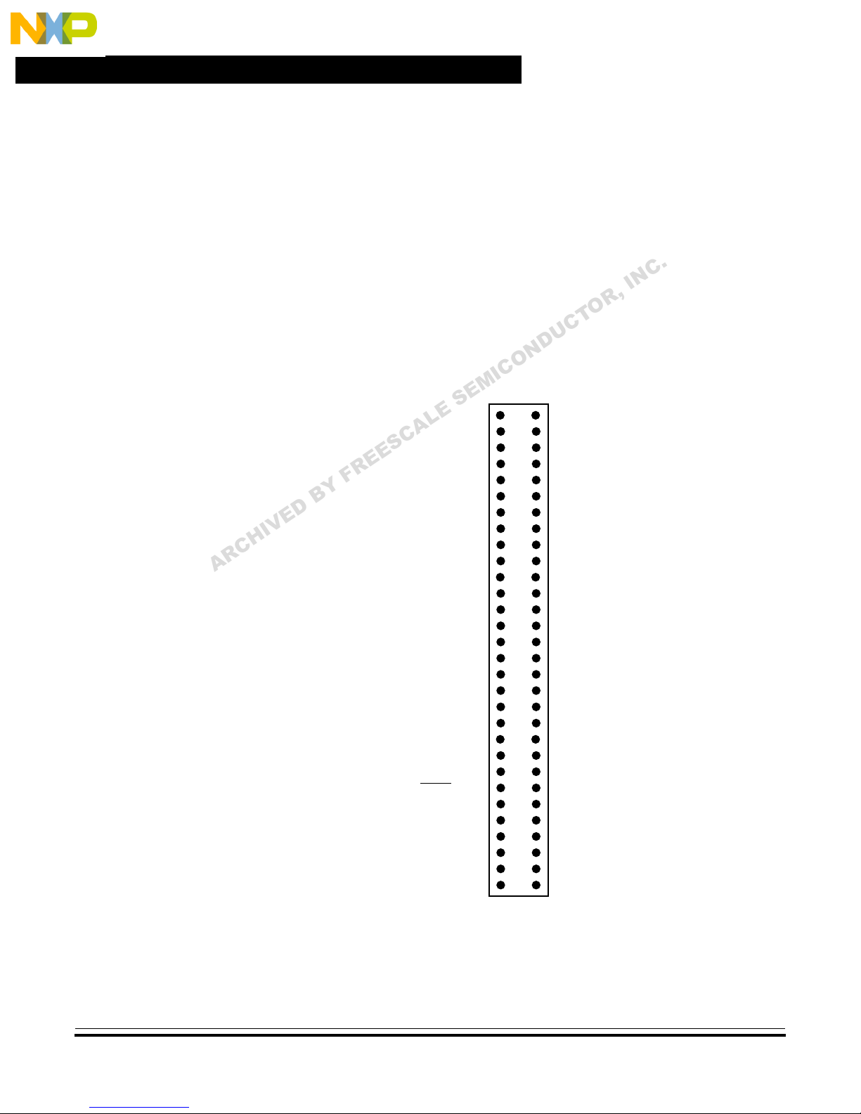
Hardware Reference
4.15 MCU Connectors
NOTE:
..
.
nc
Freescale Semiconductor, I
Freescale Semiconductor, Inc.
Two 2-row x 30-pin header connectors, J8 and J9, provide access to the MCU’s
I/0 and bus lines. These connectors are located adjacent to the prototype area for
use as described in 4.14 Prototype Area. They also provide connection points
for instrumentation probes and interfaces to target hardware. Figure 4-5 and
Figure 4-6 depict the pin assignments for J8 and J9. Table 4-5 and Table 4-6
provide descriptions of the signals.
TheEXTAL, XFC, andXTAL signals arenot directly connected to these headers
due to impedance considerations. Header footprints W37, W38, and W39 can
M
O
C
I
be used to make these connections.
S
E
E
R
F
Y
B
D
E
V
I
H
C
R
A
C
PJ6
L
PJ4
A
PJ2
PJ0
V
SSEX0
PG4
PG2
PG0
V
SSI
BKGD
PC6
PC4
PC2
PC0
PD6
PD4
PD2
PD0
PE6
PE4
PE2
PE0
NC
RESET
V
SSPLL
XTAL
PB6
PB4
PB2
PB0
E SE
11
13
15
17
19
21
23
25
27
29
31
33
35
37
39
41
43
45
47
49
51
53
55
57
59
1
3
5
7
9
N
D
U
2
4
6
8
10
12
14
16
18
20
22
24
26
28
30
32
34
36
38
40
42
44
46
48
50
52
54
56
58
60
C
O
T
PJ7
PJ5
PJ3
PJ1
V
DDEX0
PG5
PG3
PG1
V
DDI
NC
PC7
PC5
PC3
PC1
PD7
PD5
PD3
PD1
PE7
PE5
PE3
PE1
NC
XFC
V
DDPLL
EXTAL
PB7
PB5
PB3
PB1
R
,
.
C
N
I
User’s Manual M68HC12A4EVB Evaluation Board — Rev. 1
94 Hardware Reference MOTOROLA
Figure 4-5. MCU Connector J8 (Component-Side View)
For More Information On This Product,
Go to: www.freescale.com
Page 95

Freescale Semiconductor, Inc.
Hardware Reference
MCU Connectors
..
.
nc
A
R
C
H
V
SSEX1
V
SSAD
PAD6
PAD4
PAD2
PAD0
L
A
C
S
V
E
E
R
F
Y
B
D
E
V
I
SSEX2
PA6
PA4
PA2
PA0
PF6
PF4
PF2
PF0
V
RL
PH6
PH4
E SE
PH2
PH0
PS6
PS4
PS2
PS0
PT6
PT4
PT2
PT0
V
SS
V
SS
11
13
15
17
19
21
23
25
27
29
31
33
35
37
39
41
43
45
47
49
51
53
55
57
59
1
3
5
7
9
C
I
M
O
N
D
2
4
6
8
10
12
14
16
18
20
22
24
U
26
28
30
32
34
36
38
40
42
44
46
48
50
52
54
56
58
60
C
V
DDEX1
PA7
PA5
PA3
PA1
NC
PF5
PF3
PF1
V
DDAD
PAD7
O
T
PAD5
PAD3
PAD1
V
RH
PH7
PH5
PH3
PH1
V
DDEX2
PS7
PS5
PS3
PS1
PT7
PT5
PT3
PT1
V
DD
V
DD
R
,
C
N
I
Figure 4-6. MCU Connector J9 (Component-Side View)
.
Freescale Semiconductor, I
M68HC12A4EVB Evaluation Board — Rev. 1 User’s Manual
MOTOROLA Hardware Reference 95
For More Information On This Product,
Go to: www.freescale.com
Page 96
Hardware Reference
Freescale Semiconductor, Inc.
Table 4-5. MCU Connector J8 Pin Assignments
Pin Number Signal Mnemonic Signal Name and Description
..
.
nc
Freescale Semiconductor, I
A
R
C
H
1
2
3
4
5
6
7
8
9
10
11
12
13
14
15
16
17
D
18
E
V
I
19 BKGD
20 NC Not connected
21
22
23
24
25
26
27
28
F
Y
B
R
E
E
PJ6/KWUJ6
PJ7/KWUJ7
PJ4/KWUJ4
PJ5/KWUJ5
PJ2/KWUJ2
PJ3/KWUJ3
PJ0/KWUJ0
PJ1/KWUJ1
V
SSEX0
V
DDEX0
PG4/A20
PG5/A21
E SE
PG2/A18
L
A
PG3/A19
C
S
PG0/A16
PG1/A17
V
SSI
V
DDI
PC6/D14/D6
PC7/D15/D7
PC4D12/D4
PC5/D13/D5
PC2/D10/D2
PC3/D11/D3
PC0/D8/D0
PC1/D9/D1
PORT J, bits 0–7 — General-purpose I/O
or key wakeup
V
SSX/VDDX
N
connections
O
C
I
M
PORT G, bits 0–5 — General-purpose I/O
or memory expansion lines
V
SSI/VDDI
connections for the MCU
BACKGROUND — An I/O line dedicated
to the background debug function. If it is a
0 out of reset then the MCU is in special
mode. This pin can be used for
bidirectional communications with the
MCU.
PORT C, bits 0–7 — General-purpose I/O
or data bus
N
I
,
R
O
T
C
U
— External VSS and V
D
— Internal VSS and V
C
.
DD
DD
User’s Manual M68HC12A4EVB Evaluation Board — Rev. 1
96 Hardware Reference MOTOROLA
29
30
31
32
33
34
35
36
PD6/D6/KWUD6
PD7/D7/KWUD7
PD4/D4/KWUD4
PD5/D5/KWUD5
PD2/D2/KWUD2
PD3/D3/KWUD3
PD0/D0/KWUD0
PD1/D1/KWUD1
PORTD,bits 0–7 — General-purpose I/O,
data bus, or key wakeup
For More Information On This Product,
Go to: www.freescale.com
Page 97

Freescale Semiconductor, Inc.
Hardware Reference
MCU Connectors
Table 4-5. MCU Connector J8 Pin Assignments (Continued)
Pin Number Signal Mnemonic Signal Name and Description
..
.
nc
Freescale Semiconductor, I
A
R
C
H
37
38
39
40
41
42
43
44
45
46
47 RESET
48 XFC
49
50
B
D
E
51 XTAL
V
I
52 EXTAL
53
54
55
56
57
58
59
60
PE6/MODB/IPIPE1
PE5/MODA/IPIPE0
E
E
R
F
Y
PE7/ARSIE
PE4/E
PE2/RW
PE3/LSTRB
PE0/XIRQ
PE1/IRQ
NC
NC
E SE
L
A
C
S
V
SSPLL
V
DDPLL
PB6/A6
PB7/A7
PB4/A4
PB5/A5
PB2/A2
PB3/A3
PB0/A0
PB1/A1
PORT E, bits 0–7 — General-purpose I/O
or external signals such as mode select,
auxiliary reset, E clock, read/write, strobe
low, XIRQ, and IRQ
,
R
O
T
C
U
D
Not connected
N
O
C
I
Reset — Active-low bidirectional control
M
line used to initialize the MCU
XFC — Optional filter-capacitor
connection for PLL circuit
V
SSPLL/VDDPLL
connections for the PLL circuit
CRYSTAL OUTPUT — Crystal oscillator
output
EXTERNAL CLOCK INPUT — Crystal
oscillator input. The frequency applied to
this pin must be twice the desired bus
speed.
PORT B, bits 0–7 — General-purpose I/O
or low byte address bus
— VSS and V
.
C
N
I
DD
M68HC12A4EVB Evaluation Board — Rev. 1 User’s Manual
MOTOROLA Hardware Reference 97
For More Information On This Product,
Go to: www.freescale.com
Page 98
Hardware Reference
Freescale Semiconductor, Inc.
Table 4-6. MCU Connector J9 Pin Assignments
Pin Number Signal Mnemonic Signal Name And Description
..
.
nc
Freescale Semiconductor, I
A
R
C
H
1
2
3
4
5
6
7
8
9
10
11 PF6/CSP1
12 NC Not connected
13
14
15
16
D
E
17
V
I
18
19
20
21
22
23
24
25
26
27
28
29
30
B
Y
R
F
S
E
E
PF5/CSP0
V
SSEX1
V
DDEX1
PA6/A14
PA7/A15
PA4/A12
PA5/A13
PA2/A10
PA3/A11
PA0/A8
PA1/A9
E SE
L
A
C
PF4/CSD
PF2/CS2
PF3/CS3
PF0/CS0
PF1/CS1
V
SSAD
V
DDAD
PAD6
PAD7
PAD4
PAD5
PAD2
PAD3
PAD0
PAD1
V
RL
V
RH
V
SSX/VDDX
connections
PORT A, bits 0–7 — General-purpose I/O
or high byte address bus
N
O
C
I
M
PORT F, bit 6 — General-purpose I/O or
chip select
PORT F, bits 0–5 — General-purpose I/O
port or chip selects
V
SSAD/VDDAD
connections for the MCU’s A/D converter
PORT AD — A/D converter channel or
general-purpose I/O
VOLTAGE REFERENCE, LOW and HIGH
— Reference voltages for the MCU’s A/D
converter. These can improve the
accuracy of A/D conversions.
— External VSS and V
I
,
R
O
T
C
U
D
— VSS and V
N
C
DD
.
DD
User’s Manual M68HC12A4EVB Evaluation Board — Rev. 1
98 Hardware Reference MOTOROLA
31
32
33
34
35
36
37
38
PH6/KWUH6
PH7/KWUH7
PH4/KWUH4
PH5/KWUH5
PH2/KWUH2
PH3/KWUH3
PH0/KWUH0
PH1/KWUH1
PORT H, bits 0–7 — General-purpose I/O
or key wakeup
For More Information On This Product,
Go to: www.freescale.com
Page 99

Freescale Semiconductor, Inc.
Hardware Reference
Schematics
Table 4-6. MCU Connector J9 Pin Assignments (Continued)
Pin Number Signal Mnemonic Signal Name And Description
..
.
nc
4.16 Schematics
A
R
C
H
39
340
41
42
43
44
45
46
47
48
49
50
51
52
53
54
55
56
D
E
V
57
I
58
59
60
B
Y
R
F
V
SSEX2
V
DDEX2
PS6/SCK
PS7/SS
PS4/MISO
PS5/MOSI
PS2/RXD1
PS3/TXD1
PS0/RXD0
PS1/TXD0
PT6/IOC6
PT7/IOC7/PAIN
S
E
E
E SE
PT4/IOC4
L
A
PT5/IOC5
C
PT2/IOC2
PT3/IOC3
PT0/IOC0
PT1/IOC1
V
SS
V
DD
V
SS
V
DD
V
SSX/VDDX
connections
PORT S, bits 0–7 — General-purpose I/O
or multiple serial interface (MSI) lines.The
MSI lines consist of serial peripheral and
serial communication interfaces. The
signal functions are serial clock, slave
select, master in/slave out, master
out/slave in, receiver data input, and
N
transmitter data out.
O
C
I
M
PORT T, bits 0–7 — General-purpose I/O
or timer lines
VSS/VDD— EVB system return (VSS) and
power (VDD)
— External VSS and V
I
,
R
O
T
C
U
D
N
C
.
The schematics for the M68HC12A4EVB are provided here for your reference.
DD
Freescale Semiconductor, I
M68HC12A4EVB Evaluation Board — Rev. 1 User’s Manual
MOTOROLA Hardware Reference 99
For More Information On This Product,
Go to: www.freescale.com
Page 100
Freescale Semiconductor, I
Freescale Semiconductor, Inc.
For More Information On This Product,
Go to: www.freescale.com
nc
.
..
A
R
C
H
I
V
E
D
B
Y
F
R
E
E
S
C
A
L
E SE
M
I
C
O
N
D
U
C
T
O
R
,
I
N
C
.
 Loading...