

Page 1
Reference Guide
M68HC08RG/AD
Rev . 2, 3/ 2002
M68HC08
Family Reference Guide
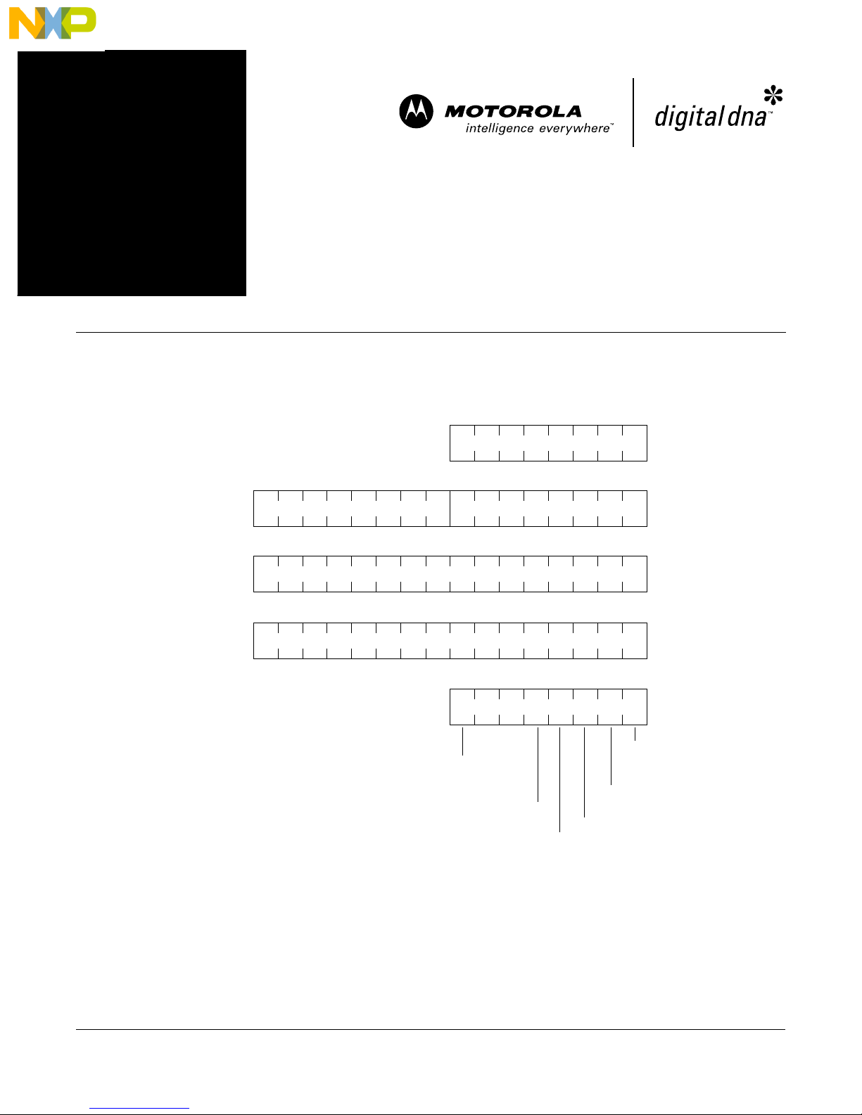
Programming Model
nc...
I
Freescale Semiconductor, Inc.
70
cale Semiconductor,
Frees
A ACCUMULATOR (A)
15 8 7 0
H X INDEX REGISTER (H:X)
15 0
15 0
70
V11HINZC
TWO’ S COMPLEME NT OVERFLOW
FLAG (V)
ZERO FLAG (Z)
HALF-CAR RY FL AG (H )
NEGATIVE FLAG (N)
INTERRUP T MA SK ( I)
STACK POINTER (SP)
PROGRAM COUNTE R (PC)
CONDITION CODE
REGISTER (CCR)
CARRY/BORROW FLAG (C)
Figure 1. Programming Model
© Motorola, In c., 2002
For More Information On This Product,
Go to: www.freescale.com
Page 2
M68HC08RG/AD
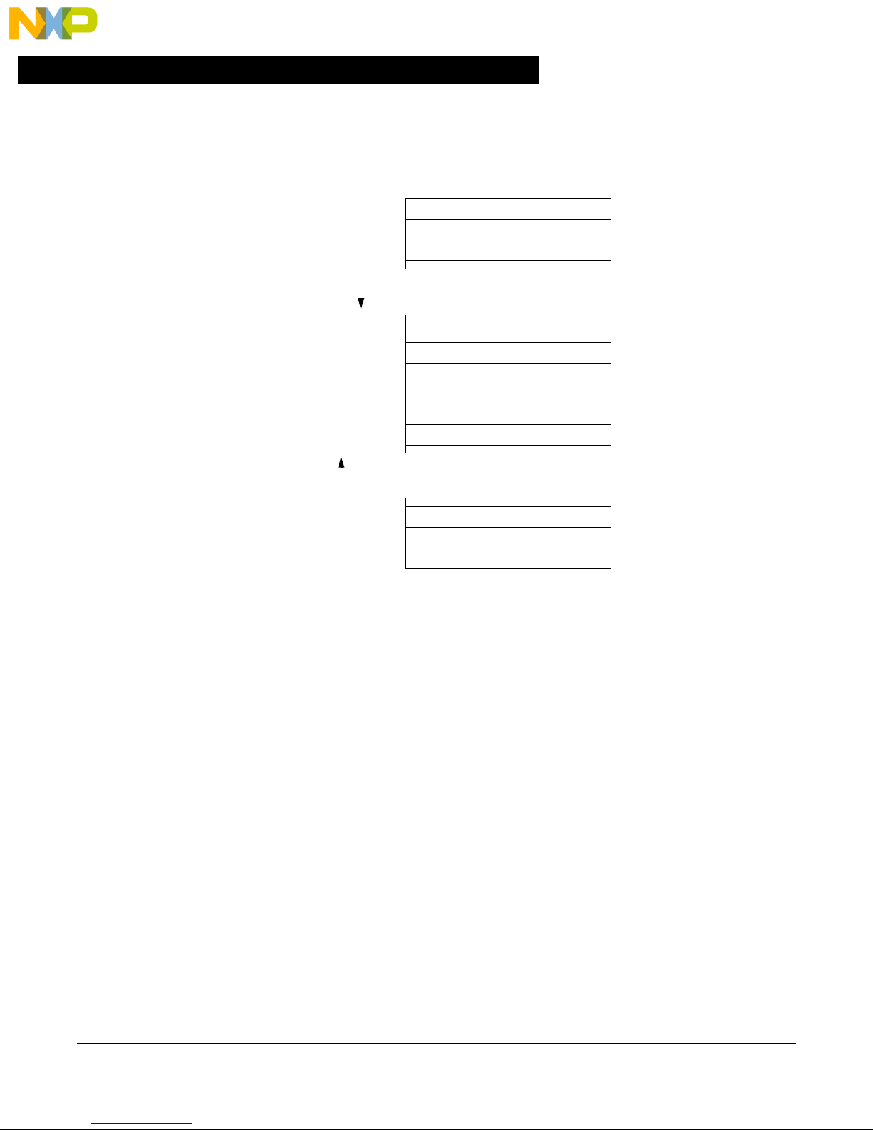
Stacking
nc...
I
Freescale Semiconductor, Inc.
UNSTACKING
ORDER
5
1
4
2
3
3
2
4
1
5
70
•
•
•
CONDITION CODE RE G ISTE R
ACCUMULATOR
INDEX REGISTER (LOW BYTE X)
PROGRAM COUNTER HIGH
PROGRAM COUNTER LOW
(1)
cale Semiconductor,
Frees
•
•
STACKING
ORDER
1. High byte (H) of index register is not stacked.
•
$00FF (DEFAULT ADDRESS
ON RESET)
Figure 2. Interrupt Stack Frame
NOTE: To maintain compatibility with the M6805 Family, H (the high byte of the index
register) is n ot stacked during interru pt processing . If th e interrupt se rv ic e
routine modifies H or uses the indexed addressing mode, it is
the user’s responsibility to save and restor e it prior to returning.
IRQINT PSHH
|
|Interrupt service routine
|
|
PULH
RTI
2 M68HC08 Family Reference Guide MOTOROLA
Figure 3. H Register Storage
For More Information On This Product,
Go to: www.freescale.com
Page 3
Freescale Semiconductor, Inc.
Interrup t Vect or Lo cat io ns
Address Reset Priority
FFFE Reset 1
FFFC SWI 2
FFFA IREQ[0] 3
:::
FF02 IREQ[124] 127
FF00 IREQ[125] 128
Notation Used in Instruction Set Summary
nc...
I
See Table 2 for the instruction set summary.
M68HC08RG/AD
Table 1. M68HC08 Vectors
cale Semiconductor,
Frees
Operators
= Contents of register or memory location shown inside parentheses
( )
= Is loaded with (read: “gets”)
←
= Boolean AND
&
= Boolean OR
|
= Boolean exclusive OR
⊕
= Multiply
×
= Divide
÷
= Concatenate
:
=Add
+
= Negate (two’s complement)
–
= Sign extend
«
CPU Registers
A = Accumulator
CCR = Condition code register
H = Index register, higher order (most significant) eight bits
X = Index register, lower order (least significant) eight bits
PC = Program counter
PCH = Prog ram counter, higher order (most significant) eight bits
PCL = Program count er, lower order (least significant) eight bits
SP = Stack pointer
MOTOROLA M68HC08 Family Reference Guide 3
For More Information On This Product,
Go to: www.freescale.com
Page 4

M68HC08RG/AD
nc...
I
Freescale Semiconductor, Inc.
Memory and Addressing
M:M + $0001
Condition Code Register (CCR) Bits
=Two’s complement overflow indicator, bit 7
V
= Half carry, bit 4
H
= Interrupt mask, bit 3
I
= Negative i n d icator, bit 2
N
= Zero indicator , bit 1
Z
= Carry/borrow, bit 0 (carry out of bit 7)
C
= A memory location or absolute data, depending on addressing
M
mode
= A 16-bit value in two consecutive memory locations. The higher-
order (most significant) eight bits are located at the address of M,
and the lower-order (least significant) eight bits are located at the
next higher sequential address.
= The relative offset, which is the two’s complement number stored
rel
in the last byte of machine code corresponding to a branch
instruction
cale Semiconductor,
Frees
Bit Status BEFORE Execution of an Instruction (n = 7, 6, 5, ... 0)
=Bit n of memory location used in operation
Mn
=Bit n of accumulator
An
=Bit n of index register H
Hn
=Bit n of index register X
Xn
=Bit n of the source operand (M, A, or X)
bn
1. For 2-byte operati ons such as LDHX, STHX, and CPHX, n = 15 refers to bit 15 of the
2-byte word or bit 7 of the most significant (first) byte.
Bit Status A F TE R Execution of an Instructio n
=Bit n of the result of an operation (n = 7, 6, 5, … 0)
Rn
1. For 2-byte operations such as LDHX, STHX, and CPHX, n = 15 refers to bit 15 of the
2-byte word or bit 7 of the most significant (first) byte.
CCR Activity Figure Notation
– = Bit not affected
0 = Bit forced to 0
1 = Bit forced to 1
= Bit set or cleared according to results of operation
U = Undefined after the operation
(1)
(1)
4 M68HC08 Family Reference Guide MOTOROLA
For More Information On This Product,
Go to: www.freescale.com
Page 5

Freescale Semiconductor, Inc.
Machine Coding Notation
dd = Low-order eight bits of a direct address $0000–$00FF (high byte assumed
ee = Upper eight bits of 16-bit offset
ff = Lower eight bits of 16-bit offset or 8-bit offset
ii = One byte of immediate data
jj = High-order byte of a 16-bit immediate data value
kk = Low-order byte of a 16-bit immediate data value
hh = High-order byte of 16-bit extended address
ll = Low-order byte of 16-bit extended address
rr = Relative offset
M68HC08RG/AD
to be $00)
nc...
I
cale Semiconductor,
Frees
Explanation of Italic Expressions in Source Form Col umn
n = Any label or expression that evaluates to a single integer in the range 0–7
opr8i = Any label or expression that evaluates to an 8-bit immediate value
opr16i = Any label or expression that evaluates to a 16-bit immediate value
opr8a = Any label or expression that evaluates to an 8-bit value. The instruction
treats this 8-bit value as the low order eight bits of an address in the direct
page of the 64-Kbyte address space ($00xx).
opr16a = Any label or expression that evaluates to a 16-bit value. The instruction
treats this value as an address in the 64-Kbyte address space.
oprx8 = Any label or expression that evaluates to an unsigned 8-bit value; used
for indexed addressing
oprx16 = Any label or expression that evaluates to a 16-bit value. Since the
MC68HC08S has a 16-bit address bus, this can be either a signed or an
unsigned value.
rel = Any label or expression that refers to an address that is within –128 to
+127 locations from the next address after the last byte of object code for
the current instruction. The assembler will calculate the 8-bit signed
offset and include it in the object code for this instruction.
Address Modes
INH = Inherent (no operands)
IMM = 8-bit or 16-bit immediate
DIR = 8-bit direct
EXT = 16-bit extended
IX = 16-bit indexed no offset
IX+ = 16-bit indexed no offset, post increment (CBEQ and MOV only)
IX1 = 16-bit indexed with 8-bit offset from H:X
IX1+ = 16-bit indexed with 8-bit offset, post increment (CBEQ only)
IX2 = 16-bit indexed with 16-bit offset from H:X
REL = 8-bit relative offset
SP1 = Stack pointer relative with 8-bit offset
SP2 = Stack pointer relative with 16-bit offset
MOTOROLA M68HC08 Family Reference Guide 5
For More Information On This Product,
Go to: www.freescale.com
Page 6
M68HC08RG/AD
Freescale Semiconductor, Inc.
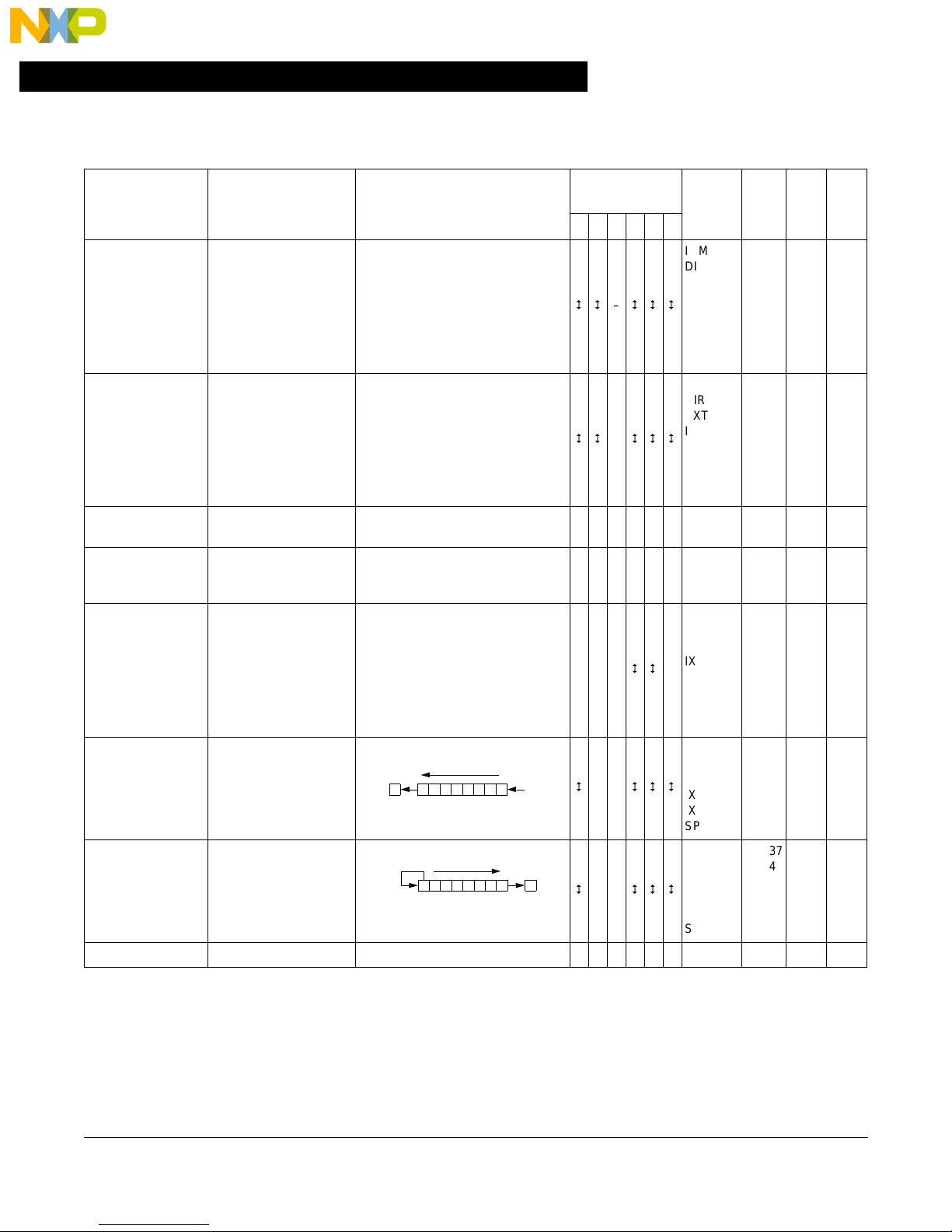
Table 2. Instruction Set Summ ar y (Sheet 1 o f 8)
nc...
I
cale Semiconductor,
Frees
Source
Form
ADC #opr8i
ADC opr8a
ADC opr16a
ADC oprx16,X
ADC oprx8,X
ADC ,X
ADC oprx16,SP
ADC oprx8,SP
ADD #opr8i
ADD opr8a
ADD opr16a
ADD oprx16,X
ADD oprx8,X
ADD ,X
ADD oprx16,SP
ADD oprx8,SP
AIS #opr8i
AIX #opr8i
AND #opr8i
AND opr8a
AND opr16a
AND oprx16,X
AND oprx8,X
AND ,X
AND oprx16,SP
AND oprx8,SP
ASL opr8a
ASLA
ASLX
ASL oprx8,X
ASL ,X
ASL oprx8,SP
ASR opr8a
ASRA
ASRX
ASR oprx8,X
ASR ,X
ASR oprx8,SP
BCC rel Branch if Carry Bit Clear Branch if (C) = 0 ––––––REL 24 rr 3
Operation Description
Add with Carry A ← (A) + (M) + (C)
Add wit hout Carry A ← (A) + (M)
Add Immediate Value
(Signed) to Stack Pointer
Add Immediate Value
(Signed) to Index
Register (H:X)
Logical AND A ← (A) & (M) 0 ––
Arithmetic Shift Left
(Same as LSL)
Arithmetic Shift Right
M is sign extended to a 16-bit value
M is sign extended to a 16-bit value
SP ← (SP) + (M)
H:X ← (H:X) + (M)
C
b7
b7
0
b0
C
b0
on CCR
IMM
DIR
EXT
IX2
IX1
IX
SP2
SP1
IMM
DIR
EXT
IX2
IX1
IX
SP2
SP1
IMM
DIR
EXT
IX2
IX1
IX
SP2
SP1
DIR
INH
INH
IX1
IX
SP1
DIR
INH
INH
IX1
IX
SP1
Mode
Address
Opcode
A9
B9
C9
D9
E9
F9
9ED9
9EE9
AB
BB
CB
DB
EB
FB
9EDB
9EEB
A4
B4
C4
D4
E4
F4
9ED4
9EE4
38
48
58
68
78
9E68
37
47
57
67
77
9E67
Operand
ii
dd
hh ll
ee ff
ff
ee ff
ff
ii
dd
hh ll
ee ff
ff
ee ff
ff
ii
dd
hh ll
ee ff
ff
ee ff
ff
dd
ff
ff
dd
ff
ff
VH INZC
–
–
––––––IMM A7 ii 2
––––––IMM AF ii 2
–
––
––
Effect
Cycles
2
3
4
4
3
2
5
4
2
3
4
4
3
2
5
4
2
3
4
4
3
2
5
4
4
1
1
4
3
5
4
1
1
4
3
5
6 M68HC08 Family Reference Guide MOTOROLA
For More Information On This Product,
Go to: www.freescale.com
Page 7

Freescale Semiconductor, Inc.
Table 2. Instruction Set Summ ar y (Sheet 2 o f 8)
M68HC08RG/AD
nc...
I
cale Semiconductor,
Frees
Source
Form
BCLR n,opr8a Clear Bit n in Memory Mn ← 0 ––––––
BCS rel
BEQ rel Branch if Equal Branch if (Z) = 1 ––––––REL 27 rr 3
BGE rel
BGT rel
BHCC rel
BHCS rel
BHI rel Branch if Higher Branch if (C) | (Z) = 0 ––––––REL 22 rr 3
BHS rel
BIH rel Branch if IRQ Pin High Branch if IRQ pin = 1 ––––––REL 2F rr 3
BIL rel Branch if IRQ Pin Low Branch if IRQ pin = 0 ––––––REL 2E rr 3
BIT #opr8i
BIT opr8a
BIT opr16a
BIT oprx16,X
BIT oprx8,X
BIT ,X
BIT oprx16,SP
BIT oprx8,SP
BLE rel
BLO rel
BLS rel Branch if Lower or Same Branch if (C) | (Z) = 1 ––––––REL 23 rr 3
BLT rel
BMC rel
BMI rel Branch if Minus Branch if (N) = 1 ––––––REL 2B rr 3
Operation Description
Branch if Carry Bit Set
(Same as BLO)
Branch if Greater Than or
Equal To
(Signed O pe r an ds )
Branch if Greater Than
(Signed O pe r an ds )
Branch if Half Carry Bit
Clear
Branch if Half Carry Bit
Set
Branch if Higher or Same
(Same as BCC)
Bit Test
Branch if Less Than
or Equal To
(Signed O pe r an ds )
Branch if Lower
(Same as BCS)
Branch if Less Than
(Signed O pe r an ds )
Branch if Interrupt Mask
Clear
Branch if (N ⊕ V) = 0 ––––––REL 90 rr 3
Branch if (Z) | (N ⊕ V) = 0 ––––––REL 92 rr 3
(CCR Updated but Operands
Branch if (Z) | (N ⊕ V) = 1 ––––––REL 93 rr 3
Branch if (N ⊕ V ) = 1 ––––––REL 91 rr 3
Branch if (C) = 1 ––––––REL 25 rr 3
Branch if (H) = 0 ––––––REL 28 rr 3
Branch if (H) = 1 ––––––REL 29 rr 3
Branch if (C) = 0 ––––––REL 24 rr 3
(A) & (M)
Not Changed)
Branch if (C) = 1 ––––––REL 25 rr 3
Branch if (I) = 0 ––––––REL 2C rr 3
Effect
on CCR
VH INZC
0 ––
–
Address
DIR (b0)
DIR (b1)
DIR (b2)
DIR (b3)
DIR (b4)
DIR (b5)
DIR (b6)
DIR (b7)
IMM
DIR
EXT
IX2
IX1
IX
SP2
SP1
Mode
Opcode
11
13
15
17
19
1B
1D
1F
A5
B5
C5
D5
E5
F5
9ED5
9EE5
Operand
dd
dd
dd
dd
dd
dd
dd
dd
ii
dd
hh ll
ee ff
ff
ee ff
ff
Cycles
4
4
4
4
4
4
4
4
2
3
4
4
3
2
5
4
MOTOROLA M68HC08 Family Reference Guide 7
For More Information On This Product,
Go to: www.freescale.com
Page 8

M68HC08RG/AD
Freescale Semiconductor, Inc.
Table 2. Instruction Set Summ ar y (Sheet 3 o f 8)
nc...
I
cale Semiconductor,
Frees
Source
Form
BMS rel
BNE rel Branch if Not Equal Branch if (Z) = 0 ––––––REL 26 rr 3
BPL rel Branch if Plus Branch if (N) = 0 ––––––REL 2A rr 3
BRA rel Branch Always No Test ––––––REL 20 rr 3
BRCLR n,opr8a,rel
BRN rel Branch Never Uses 3 Bus Cycles ––––––REL 21 rr 3
BRSET n,opr8a,rel
BSET n,opr8a Set Bit n in Memory Mn ← 1 ––––––
BSR rel Branch to Subroutine
CBEQ opr8a,rel
CBEQA #opr8i,rel
CBEQX #opr8i,rel
CBEQ oprx8,X+,rel
CBEQ ,X+,rel
CBEQ oprx8,SP,rel
CLC Clear Carry Bit C ← 0 –––––0INH 98 1
CLI Clear Interrupt Mask Bit I ← 0 ––0 –––INH 9A 2
Operation Description
Branch if Interrupt Mask
Set
Branch if Bit n in Memory
Clear
Branch if Bit n in Memory
Set
Compare and Branch if
Equal
Branch if (Mn) = 0 –––––
Branch if (Mn) = 1 –––––
PC ← (PC) + $0002
push (PCL); SP ← (SP) – $0001
push (PCH); SP ← (SP) – $0001
Branch if (A) = (M)
Branch if (A) = (M)
Branch if (X) = (M)
Branch if (A) = (M)
Branch if (A) = (M)
Branch if (A) = (M)
Branch if (I) = 1 ––––––REL 2D rr 3
PC ← (PC) + rel
Effect
on CCR
VH INZC
––––––REL AD rr 4
––––––
Address
DIR (b0)
DIR (b1)
DIR (b2)
DIR (b3)
DIR (b4)
DIR (b5)
DIR (b6)
DIR (b7)
DIR (b0)
DIR (b1)
DIR (b2)
DIR (b3)
DIR (b4)
DIR (b5)
DIR (b6)
DIR (b7)
DIR (b0)
DIR (b1)
DIR (b2)
DIR (b3)
DIR (b4)
DIR (b5)
DIR (b6)
DIR (b7)
DIR
IMM
IMM
IX1+
IX+
SP1
Mode
Opcode
01
03
05
07
09
0B
0D
0F
00
02
04
06
08
0A
0C
0E
10
12
14
16
18
1A
1C
1E
31
41
51
61
71
9E61
Operand
dd rr
dd rr
dd rr
dd rr
dd rr
dd rr
dd rr
dd rr
dd rr
dd rr
dd rr
dd rr
dd rr
dd rr
dd rr
dd rr
dd
dd
dd
dd
dd
dd
dd
dd
dd rr
ii rr
ii rr
ff rr
rr
ff rr
5
5
5
5
5
5
5
5
5
5
5
5
5
5
5
5
4
4
4
4
4
4
4
4
5
4
4
5
4
6
Cycles
8 M68HC08 Family Reference Guide MOTOROLA
For More Information On This Product,
Go to: www.freescale.com
Page 9

Freescale Semiconductor, Inc.
Table 2. Instruction Set Summ ar y (Sheet 4 o f 8)
M68HC08RG/AD
nc...
I
cale Semiconductor,
Frees
Source
Form
CLR opr8a
CLRA
CLRX
CLRH
CLR oprx8,X
CLR ,X
CLR oprx8,SP
CMP #opr8i
CMP opr8a
CMP opr16a
CMP oprx16,X
CMP oprx8,X
CMP ,X
CMP oprx16,SP
CMP oprx8,SP
COM opr8a
COMA
COMX
COM oprx8,X
COM ,X
COM oprx8,SP
CPHX #opr
CPHX opr
CPX #opr8i
CPX opr8a
CPX opr16a
CPX oprx16,X
CPX oprx8,X
CPX ,X
CPX oprx16,SP
CPX oprx8,SP
DAA
DBNZ opr8a,rel
DBNZA rel
DBNZX rel
DBNZ oprx8,X,rel
DBNZ ,X,rel
DBNZ oprx8,SP,rel
DEC opr8a
DECA
DECX
DEC oprx8,X
DEC ,X
DEC oprx8,SP
DIV Divide
Clear
Compar e Accumulator
with Memory
Complement
(One’s Complement)
Compar e Index Register
(H:X) with Memory
Compar e X (Index
Register Low) with
Memory
Decimal Adjust
Accumulator After ADD or
ADC of BCD Values
Decrement and Branch if
Not Zero
Decrement
Operation Description
M ← $00
A ← $00
X ← $00
H ← $00
M ← $00
M ← $00
M ← $00
(A) – (M)
(CCR Updated But Operands Not
Changed)
)= $FF – (M)
M ← (M
) = $FF – (A)
A ← (A
) = $FF – (X)
X ← (X
) = $FF – (M)
M ← (M
) = $FF – (M)
M ← (M
) = $FF – (M)
M ← (M
(H:X) – (M:M + $0001)
(CCR Updated But Operands Not
Changed)
(CCR Updated But Operands Not
(X) – (M)
Changed)
(A)
10
Decrement A, X, or M
Branch if (result) ≠ 0
DBNZX Affec ts X Not H
M ← (M) – $01
A ← (A) – $01
X ← (X) – $01
M ← (M) – $01
M ← (M) – $01
M ← (M) – $01
A ← (H:A)÷(X)
H ← Remainder
Effect
on CCR
VH INZC
0 ––01–
––
0 ––
––
––
U ––
––––––
––
––––
1
–
Mode
Address
DIR
INH
INH
INH
IX1
IX
SP1
IMM
DIR
EXT
IX2
IX1
IX
SP2
SP1
DIR
INH
INH
IX1
IX
SP1
IMM
DIR
IMM
DIR
EXT
IX2
IX1
IX
SP2
SP1
INH 72 2
DIR
INH
INH
IX1
IX
SP1
DIR
INH
INH
IX1
IX
SP1
INH 52 7
Opcode
3F
dd
4F
5F
8C
6F
ff
7F
9E6F
ff
A1
ii
B1
dd
C1
hh ll
D1
ee ff
E1
ff
F1
9ED1
ee ff
9EE1
ff
33
dd
43
53
63
ff
73
9E63
ff
6575jj ii+1dd3
A3
ii
B3
dd
C3
hh ll
D3
ee ff
E3
ff
F3
9ED3
ee ff
9EE3
ff
3B
dd rr
4B
rr
5B
rr
6B
ff rr
7B
rr
9E6B
ff rr
3A
dd
4A
5A
6A
ff
7A
9E6A
ff
Operand
Cycles
3
1
1
1
3
2
4
2
3
4
4
3
2
5
4
4
1
1
4
3
5
4
2
3
4
4
3
2
5
4
5
3
3
5
4
6
4
1
1
4
3
5
MOTOROLA M68HC08 Family Reference Guide 9
For More Information On This Product,
Go to: www.freescale.com
Page 10

M68HC08RG/AD
Freescale Semiconductor, Inc.
Table 2. Instruction Set Summ ar y (Sheet 5 o f 8)
nc...
I
cale Semiconductor,
Frees
Source
Form
EOR #opr8i
EOR opr8a
EOR opr16a
EOR oprx16,X
EOR oprx8,X
EOR ,X
EOR oprx16,SP
EOR oprx8,SP
INC opr8a
INCA
INCX
INC oprx8,X
INC ,X
INC oprx8,SP
JMP opr8a
JMP opr16a
JMP oprx16,X
JMP oprx8,X
JMP ,X
JSR opr8a
JSR opr16a
JSR oprx16,X
JSR oprx8,X
JSR ,X
LDA #opr8i
LDA opr8a
LDA opr16a
LDA oprx16,X
LDA oprx8,X
LDA ,X
LDA oprx16,SP
LDA oprx8,SP
LDHX #opr
LDHX opr
LDX #opr8i
LDX opr8a
LDX opr16a
LDX oprx16,X
LDX oprx8,X
LDX ,X
LDX oprx16,SP
LDX oprx8,SP
LSL opr8a
LSLA
LSLX
LSL oprx8,X
LSL ,X
LSL oprx8,SP
Effect
Operation Description
on CCR
VH INZC
Exclus iv e OR
Memory with
Accumulator
Increment
Jump PC ← Jump Address ––––––
PC ← (PC) + n (n = 1, 2, or 3)
Jump to Subroutine
Load Accumulator from
Memory
Load Index Register (H:X)
from Memory
Load X (Index Register
Low) from Memory
Logical Shift Left
(Same as ASL)
Push (PCL); SP ← (SP) – $0001
Push (PCH); SP ← (SP) – $0001
A ← (A ⊕ M) 0 ––
M ← (M) + $01
A ← (A) + $01
X ← (X) + $01
M ← (M) + $01
M ← (M) + $01
M ← (M) + $01
PC ← Unconditional Address
A ← (M) 0 ––
H:X ← (M:M + $0001) 0 ––
X ← (M) 0 ––
C
b7
0
b0
––––––
––
––
–
–
–
–
–
IMM
DIR
EXT
IX2
IX1
IX
SP2
SP1
DIR
INH
INH
IX1
IX
SP1
DIR
EXT
IX2
IX1
IX
DIR
EXT
IX2
IX1
IX
IMM
DIR
EXT
IX2
IX1
IX
SP2
SP1
IMM
DIR
IMM
DIR
EXT
IX2
IX1
IX
SP2
SP1
DIR
INH
INH
IX1
IX
SP1
Mode
Address
Opcode
A8
ii
B8
dd
C8
hh ll
D8
ee ff
E8
ff
F8
9ED8
ee ff
9EE8
ff
3C
dd
4C
5C
6C
ff
7C
9E6C
ff
BC
dd
CC
hh ll
DC
ee ff
EC
ff
FC
BD
dd
CD
hh ll
DD
ee ff
ED
ff
FD
A6
ii
B6
dd
C6
hh ll
D6
ee ff
E6
ff
F6
9ED6
ee ff
9EE6
ff
4555ii jjdd3
AE
ii
BE
dd
CE
hh ll
DE
ee ff
EE
ff
FE
9EDE
ee ff
9EEE
ff
38
dd
48
58
68
ff
78
9E68
ff
Operand
Cycles
2
3
4
4
3
2
5
4
4
1
1
4
3
5
2
3
4
3
3
4
5
6
5
4
2
3
4
4
3
2
5
4
4
2
3
4
4
3
2
5
4
4
1
1
4
3
5
10 M68HC08 Family Reference Guide MOTOROLA
For More Information On This Product,
Go to: www.freescale.com
Page 11

Freescale Semiconductor, Inc.
Table 2. Instruction Set Summ ar y (Sheet 6 o f 8)
M68HC08RG/AD
nc...
I
cale Semiconductor,
Frees
Source
Form
LSR opr8a
LSRA
LSRX
LSR oprx8,X
LSR ,X
LSR oprx8,SP
MOV opr8a,opr8a
MOV opr8a,X+
MOV #opr8i,opr8a
MOV ,X+,opr8a
MUL Unsigned mult iply X:A ← (X) × (A) – 0 –––0INH 42 5
NEG opr8a
NEGA
NEGX
NEG oprx8,X
NEG ,X
NEG oprx8,SP
NOP No Operation Uses 1 Bus Cycle ––––––INH 9D 1
NSA
ORA #opr8i
ORA opr8a
ORA opr16a
ORA oprx16,X
ORA oprx8,X
ORA ,X
ORA oprx16,SP
ORA oprx8,SP
PSHA
PSHH
PSHX
PULA
PULH
PULX
ROL opr8a
ROLA
ROLX
ROL oprx8,X
ROL ,X
ROL oprx8,SP
Operation Description
Logical Shift Right
(M)
Move
Negate
(Two’s Complement)
Nibble Swap
Accumulator
Inclusi ve OR Accumul ator
and Memory
Push Accumulator onto
Stack
Push H (Index Register
High) onto Stack
Push X (Index Register
Low) onto Stack
Pull Accumulator from
Stack
Pull H (Index Register
High) from Stack
Pull X ( Index Register
Low) from Stack
Rotate Left through Carry
H:X ← (H:X) + $0001 in
IX+/DIR and DIR/IX+ Modes
M ← – (M) = $00 – (M)
A ← – (A) = $00 – (A)
X ← – (X) = $00 – (X)
M ← – (M) = $00 – (M)
M ← – (M) = $00 – (M)
M ← – (M) = $00 – (M)
A ← (A[3:0]:A[7:4]) ––––––INH 62 3
Push (A); SP ← (SP) – $0001 –––––– INH 87 2
Push (H); SP ← (SP) – $0001 ––––––INH 8B 2
Push (X); SP ← (SP) – $0001 ––––––INH 89 2
SP ← (SP + $0001); Pull (A) ––––––INH 86 2
SP ← (SP + $0001); Pull (H) ––––––INH 8A 2
SP ← (SP + $0001); Pull (X) ––––––INH 88 2
C
C0
b7
destination
A ← (A) | (M) 0 ––
b7
← (M)
b0
source
b0
on CCR
VH INZC
––0
0 ––
––
––
–
–
Address
DIR
INH
INH
IX1
IX
SP1
DIR/DIR
DIR/IX+
IMM/DIR
IX+/DIR
DIR
INH
INH
IX1
IX
SP1
IMM
DIR
EXT
IX2
IX1
IX
SP2
SP1
DIR
INH
INH
IX1
IX
SP1
Mode
Opcode
34
44
54
64
74
9E64
4E
5E
6E
7E
30
40
50
60
70
9E60
AA
BA
CA
DA
EA
FA
9EDA
9EEA
39
49
59
69
79
9E69
dd
ff
ff
dd dd
dd
ii dd
dd
dd
ff
ff
ii
dd
hh ll
ee ff
ff
ee ff
ff
dd
ff
ff
Operand
4
1
1
4
3
5
5
4
4
4
4
1
1
4
3
5
2
3
4
4
3
2
5
4
4
1
1
4
3
5
Effect
Cycles
MOTOROLA M68HC08 Family Reference Guide 11
For More Information On This Product,
Go to: www.freescale.com
Page 12

M68HC08RG/AD
Freescale Semiconductor, Inc.
Table 2. Instruction Set Summ ar y (Sheet 7 o f 8)
nc...
I
cale Semiconductor,
Frees
Source
Form
ROR opr8a
RORA
RORX
ROR oprx8,X
ROR ,X
ROR oprx8,SP
RSP Reset Stack Pointer
RTI Return from Interrupt
RTS Return from Subrou tine
SBC #opr8i
SBC opr8a
SBC opr16a
SBC oprx16,X
SBC oprx8,X
SBC ,X
SBC oprx16,SP
SBC oprx8,SP
SEC Set Carry Bit C ← 1 –––––1INH 99 1
SEI Set Interrupt Mask Bit I ← 1 ––1 ––– INH 9B 2
STA opr8a
STA opr16a
STA oprx16,X
STA oprx8,X
STA ,X
STA oprx16,SP
STA oprx8,SP
STHX opr Store H:X (Index Reg.) (M:M + $0001) ← (H:X) 0 ––
STOP
STX opr8a
STX opr16a
STX oprx16,X
STX oprx8,X
STX ,X
STX oprx16,SP
STX oprx8,SP
Operation Description
Rotate Right through
Carry
Subtract with Carry A ← (A) – (M) – (C)
Store Accumulato r in
Memory
Enable Interrupts:
Stop Processing
Refer to MCU
Documentation
Store X (Low 8 Bits of
Index R egister)
in Memor y
b7
SP ← $FF
(High Byte Not Affec ted )
SP ← (SP) + $0001; Pull (CCR)
SP ← (SP) + $0001; Pull (A)
SP ← (SP) + $0001; Pull (X)
SP ← (SP) + $0001; Pull (PCH)
SP ← (SP) + $0001; Pull (PCL)
SP ← SP + $0001; Pull (PCH)
SP ← SP + $0001; Pull (PCL)
I bit ← 0; Stop Processing ––0 –––INH 8E 1
b0
M ← (A) 0 ––
M ← (X) 0 ––
C
Effect
on CCR
VH INZC
––
––––––INH 9C 1
––––––INH 81 4
––
–
– DIR 35 dd 4
–
Mode
Address
DIR
INH
INH
IX1
IX
SP1
INH 80 7
IMM
DIR
EXT
IX2
IX1
IX
SP2
SP1
DIR
EXT
IX2
IX1
IX
SP2
SP1
DIR
EXT
IX2
IX1
IX
SP2
SP1
Opcode
9E66
A2
B2
C2
D2
E2
F2
9ED2
9EE2
B7
C7
D7
E7
F7
9ED7
9EE7
BF
CF
DF
EF
FF
9EDF
9EEF
36
46
56
66
76
Operand
dd
ff
ff
ii
dd
hh ll
ee ff
ff
ee ff
ff
dd
hh ll
ee ff
ff
ee ff
ff
dd
hh ll
ee ff
ff
ee ff
ff
4
1
1
4
3
5
2
3
4
4
3
2
5
4
3
4
4
3
2
5
4
3
4
4
3
2
5
4
Cycles
12 M68HC08 Family Reference Guide MOTOROLA
For More Information On This Product,
Go to: www.freescale.com
Page 13

Freescale Semiconductor, Inc.
Table 2. Instruction Set Summ ar y (Sheet 8 o f 8)
M68HC08RG/AD
nc...
I
cale Semiconductor,
Frees
Source
Form
SUB #opr8i
SUB opr8a
SUB opr16a
SUB oprx16,X
SUB oprx8,X
SUB ,X
SUB oprx16,SP
SUB oprx8,SP
SWI Software Interrupt
TAP
TAX
TPA
TST opr8a
TSTA
TSTX
TST oprx8,X
TST ,X
TST oprx8,SP
TSX Transfer SP to Index Reg. H:X ← (SP) + $0001 ––––––INH 95 2
TXA
TXS Transfer Index Reg. to SP SP ← (H:X) – $0001 ––––––INH 94 2
WAIT
Operation Description
Subtract A ← (A) – (M)
PC ← (PC) + $0001
Push (PCL); SP ← (SP) – $0001
Push (PCH); SP ← (SP) – $0001
Push (X); SP ← (SP) – $0001
Push (A); SP ← (SP) – $0001
Push (CCR); SP ← (SP) – $0001
PCH ← Inter ru pt Vector High Byte
PCL ← Interrupt Vector Low Byte
Transfer Accumulator to
CCR
Transfer Accumulator to
X (Inde x Register Low)
Transfer CCR to
Accumulator
Test for Negative or Zero
Transfer X (Index Reg.
Low) to Accumulator
Enable Interrupts; Wait
for Interrupt
I ← 1;
CCR ← (A)
X ← (A) ––––––INH 97 1
A ← (CCR) ––––––INH 85 1
(M) – $00
(A) – $00
(X) – $00
(M) – $00
(M) – $00
(M) – $00
A ← (X) ––––––INH 9F 1
I bit ← 0; Halt CPU ––0 ––– INH 8F 1
Effect
on CCR
VH INZC
––
––1 –––INH 83 9
0 ––
–
Mode
Address
IMM
DIR
EXT
IX2
IX1
IX
SP2
SP1
INH 84 2
DIR
INH
INH
IX1
IX
SP1
Opcode
A0
B0
C0
D0
E0
F0
9ED0
9EE0
3D
4D
5D
6D
7D
9E6D
Operand
ii
dd
hh ll
ee ff
ff
ee ff
ff
dd
ff
ff
Cycles
2
3
4
4
3
2
5
4
3
1
1
3
2
4
MOTOROLA M68HC08 Family Reference Guide 13
For More Information On This Product,
Go to: www.freescale.com
Page 14

Freescale Semiconductor, Inc.
M68HC08RG/AD
Addressing Modes
Inherent (INH) The inherent addre ssing mode has no opera nd because t he opcode contains
all informatio n necessary to carry out th e instruction. Mo st inherent instru ctions
are one byt e long.
Immediate (IMM) The operand in immediate mode instructions is contained in the byte(s)
immedia te ly fo llowing the opcode. The immediate value is one or two by te s ,
dependi ng on the size of the register inv olv ed in the ins t ruc t ion.
Direct (DIR) Most direc t mo de instructions can ac c es s any of the first 256 memory
nc...
I
addresses with two bytes. The first byte is the opcode, and the second byte is
the low byte of the operand address. The high byte of the address is assumed
to be $00.
Extended (EXT) Extended mode instructions are three bytes in length and can access any
address in a 64-Kbyte memory map. The first byte is the opcode. The following
two bytes are the oper and addre s s es .
Indexed (IX, IX1,
and IX2)
cale Semiconductor,
Indexed mode instructio ns acce ss d ata wi th vari abl e a ddr esses. Th e eff ect iv e
address (EA) of the operand is determined by the contents of the register (H:X)
added to a z ero, 8-bit, or 16-bit offset. F or one-byte, z ero-offset mode
instructions (IX), X (index register low) contains the low byte of the EA of the
operand . The value of H (index regist er high) is $00 if none of th e H C 08
instructio ns t hat modify H are used, assuring sou rc e c ode compat ibility with
HC05 Fam ily instructions. The sum of H :X is th e EA of the op erand. For twobyte, 8-bit offset mode instructions (IX1) the unsigned bytes in H:X added to the
unsigned byte following the opcode cons t it ut es t he EA of the operand. For
three byte, 16-bit offset mode instructions (IX2), the unsigned bytes in H:X
added to the 16-bit unsigned word following the opcode constitute the EA of the
operand.
Frees
Stack Poi n ter
(SP1 and SP2)
Stac k pointer (SP) mode ins tructions operat e like indexed instr uc tion s , except
that t he offset is added to the 16-bit SP. Stac k pointer, 8-bit offs et instructio ns
(SP1) are th ree-byte ins tr uc t ions. The EA of the operand is form ed by addin g
the unsigned byte in the SP register to the unsigned byte following the opcode.
Stack pointer, 16-bit offset instructions (SP2) are four-byte instructions. The EA
of the operand is formed by adding the unsigned bytes in the 16-bit SP register
to the 16-b it uns igned wor d fo llowing the opcode.
14 M68HC08 Family Reference Guide MOTOROLA
For More Information On This Product,
Go to: www.freescale.com
Page 15

Freescale Semiconductor, Inc.
Relative (REL) Conditio nal branch in s tr uc t ions use the relative addressing mode. The EA of
the operand depends on wheth er or not the branch is taken. If a branch is
taken, the EA of the operand is formed by adding the signed byte following the
opcode to the value of the PC, and the PC is loaded with the EA. If no branch
is taken, the EA is the contents of the PC.
M68HC08RG/AD
Memory to Memory
(IMD, DD, IX+D, and
DIX+)
nc...
I
Indexed and Indexed
8-Bit Offs et with
Post Increment
(IX+ and IX1+)
cale Semiconductor,
Opcode Map
Memory to memory immediate to direct (IMD) is a three-byte addressing mode.
The oper and in th e byte imme diatel y foll owing the opcode i s stored in the dir ect
page location addressed by the second byte following the opcode.
Memory to memory direct to direct (DD) is a three-byte addressing mode. The
oper and in the byte immediately f ollowing the op c ode is stored in the direct
page location addressed by the second byte following the opcode.
Memor y to memory indexed t o direc t with po st incr ement of H:X (IX+D) is a twobyte addr es s ing mode. T he operan d addressed by H:X is stored in the direct
page locat ion addres s ed by the byte f ollowing the opcode.
Memor y to memor y dir ect to i ndex ed w ith post incr ement of H:X ( DIX +) is a t wobyte addr es s ing mode. T he operan d in the direct page location address ed by
the byte immediately following the opcode is stored in the location addressed
by H:X.
Indexed , n o of f s et wi th pos t inc rement mode instructions (IX+ ) are two- by t e
instructions that address operands, then increment H:X. The EA of the operand
is der ive d by a ddi ng X (l ow byt e) t o H ( high b yte ). In dexe d, 8- bit offs et wi th po st
increme nt m ode instruc tio ns (I X1+) are th ree-byte ins t ruc t ions that add ress
operands with variable addresses, then increment H:X. The EA of the operand
is derived by adding X (low byte) with H (high byte).
Frees
See Table 3.
Hexadecimal to ASCII Conversion
See Table 4.
MOTOROLA M68HC08 Family Reference Guide 15
For More Information On This Product,
Go to: www.freescale.com
Page 16

M68HC08RG/AD
nc...
I
cale Semiconductor,
Frees
Freescale Semiconductor, Inc.
2
2
2
2
SUB
1IX
4
SUB
3 SP1
3
SUB
2IX1
5
SUB
4SP2
4
SUB
3IX2
4
SUB
3EXT
3
SUB
2DIR
2
SUB
2IMM
3
BGE
2REL
7
RTI
1INH
3
NEG
1IX
5
NEG
3 SP1
4
Table 3. M68HC08 Opcode Map
NEG
2IX1
1
NEGX
1INH
1
NEGA
1INH
4
NEG
2DIR
3
BRA
2REL
4
4
3
5
4
4
3
2
3
4
4
6
5
4
4
5
3
4
CMP
1IX
CMP
3 SP1
CMP
2IX1
CMP
4SP2
CMP
3IX2
CMP
3EXT
CMP
2DIR
CMP
2IMM
BLT
2REL
RTS
1INH
CBEQ
2IX+
CBEQ
4 SP1
CBEQ
3IX1+
CBEQX
3IMM
CBEQA
3IMM
CBEQ
3DIR
BRN
2REL
4
3
5
4
4
3
2
3
2
3
7
5
3
4
SBC
1IX
SBC
3 SP1
SBC
2IX1
SBC
4SP2
SBC
3IX2
SBC
3EXT
SBC
2DIR
SBC
2IMM
BGT
2REL
DAA
1INH
NSA
1INH
DIV
1INH
MUL
1INH
BHI
2REL
CPX
4
CPX
3
CPX
5
CPX
4
CPX
4
CPX
3
CPX
2
CPX
3
BLE
9
SWI
3
COM
5
COM
4
COM
1
COMX
1
COMA
4
COM
3
BLS
4
2
1IX
4
3 SP1
3
2IX1
5
4SP2
4
3IX2
4
3EXT
3
2DIR
2
2IMM
2
2REL
2
1INH
3
1IX
5
3 SP1
4
2IX1
1
1INH
1
1INH
4
2DIR
3
2REL
4
AND
1IX
AND
3 SP1
AND
2IX1
AND
4SP2
AND
3IX2
AND
3EXT
AND
2DIR
AND
2IMM
TXS
1INH
TAP
1INH
LSR
1IX
LSR
3 SP1
LSR
2IX1
LSRX
1INH
LSRA
1INH
LSR
2DIR
BCC
2REL
2
4
3
5
4
4
3
2
2
1
4
3
4
3
4
3
4
BIT
1IX
BIT
3 SP1
BIT
2IX1
BIT
4SP2
BIT
3IX2
BIT
3EXT
BIT
2DIR
BIT
2IMM
TSX
1INH
TPA
1INH
CPHX
2DIR
CPHX
3IMM
LDHX
2DIR
LDHX
3IMM
STHX
2DIR
BCS
2REL
2
4
3
5
4
4
3
2
2
3
5
4
1
1
4
3
4
LDA
1IX
LDA
3 SP1
LDA
2IX1
LDA
4SP2
LDA
3IX2
LDA
3EXT
LDA
2DIR
LDA
2IMM
PULA
1INH
ROR
1IX
ROR
3 SP1
ROR
2IX1
RORX
1INH
RORA
1INH
ROR
2DIR
BNE
2REL
2
4
3
5
4
4
3
2
1
2
3
5
4
1
1
4
3
4
STA
1IX
STA
3 SP1
STA
2IX1
STA
4SP2
STA
3IX2
STA
3EXT
STA
2DIR
AIS
2IMM
TA X
1INH
PSHA
1INH
ASR
1IX
ASR
3 SP1
ASR
2IX1
ASRX
1INH
ASRA
1INH
ASR
2DIR
BEQ
2REL
2
4
3
5
4
4
3
2
1
2
3
5
4
1
1
4
3
4
EOR
1IX
EOR
3 SP1
EOR
2IX1
EOR
4SP2
EOR
3IX2
EOR
3EXT
EOR
2DIR
EOR
2IMM
CLC
1INH
PULX
1INH
LSL
1IX
LSL
3 SP1
LSL
2IX1
LSLX
1INH
LSLA
1INH
LSL
2DIR
BHCC
2REL
2
4
3
5
4
4
3
2
1
2
3
5
4
1
1
4
3
4
ADC
1IX
ADC
3 SP1
ADC
2IX1
ADC
4SP2
ADC
3IX2
ADC
3EXT
ADC
2DIR
ADC
2IMM
SEC
1INH
PSHX
1INH
ROL
1IX
ROL
3 SP1
ROL
2IX1
ROLX
1INH
ROLA
1INH
ROL
2DIR
BHCS
2REL
2
4
3
5
4
4
3
2
2
2
3
5
4
1
1
4
3
4
ORA
1IX
ORA
3 SP1
ORA
2IX1
ORA
4SP2
ORA
3IX2
ORA
3EXT
ORA
2DIR
ORA
2IMM
CLI
1INH
PULH
1INH
DEC
1IX
DEC
3 SP1
DEC
2IX1
DECX
1INH
DECA
1INH
DEC
2DIR
BPL
2REL
2
4
3
5
4
4
3
2
2
2
4
6
5
3
3
5
3
4
ADD
ADD
ADD
ADD
ADD
ADD
ADD
ADD
SEI
PSHH
DBNZ
DBNZ
DBNZ
DBNZX
DBNZA
DBNZ
BMI
2
1IX
3 SP1
3
2IX1
4SP2
4
3IX2
3
3EXT
2
2DIR
2IMM
1
1INH
1
1INH
3
2IX
5
4 SP1
4
3IX1
1
2INH
1
2INH
4
3DIR
3
2REL
4
JMP
1IX
JMP
2IX1
JMP
3IX2
JMP
3EXT
JMP
2DIR
RSP
1INH
CLRH
1INH
INC
1IX
INC
3 SP1
INC
2IX1
INCX
1INH
INCA
1INH
INC
2DIR
BMC
2REL
4
5
6
5
4
4
1
2
4
3
1
1
3
3
4
JSR
1IX
JSR
2IX1
JSR
3IX2
JSR
3EXT
JSR
2DIR
BSR
2REL
NOP
1INH
TST
1IX
TST
3 SP1
TST
2IX1
TSTX
1INH
TSTA
1INH
TST
2DIR
BMS
2REL
2
4
3
5
4
4
3
2
1
4
4
4
5
3
4
LDX
1IX
LDX
3 SP1
LDX
2IX1
LDX
4SP2
LDX
3IX2
LDX
3EXT
LDX
2DIR
LDX
2IMM
*
STOP
1INH
MOV
2IX+D
MOV
3IMD
MOV
2DIX+
MOV
3DD
BIL
2REL
2
4
3
5
4
4
3
2
1
1
2
4
3
1
1
3
3
4
STX
1IX
STX
3 SP1
STX
2IX1
STX
4SP2
STX
3IX2
STX
3EXT
STX
2DIR
AIX
2IMM
TXA
1INH
WAIT
1INH
CLR
1IX
CLR
3 SP1
CLR
2IX1
CLRX
1INH
CLRA
1INH
CLR
2DIR
BIH
2REL
HC08 Cycles
Opcode Mnemonic
Number of Bytes / Addressing Mode
2
F
SUB
1IX
0
High Byte of Opcode in Hexadecimal
Low Byte of Opcode in Hexadecimal
Bit-Manipulation Branch Read -Modify-Write Control Register/Memo ry
DIR DIR REL DIR INH INH IX1 SP1 IX INH INH IMM DIR EX T IX2 SP2 IX1 SP1 IX
HIGH
BSET0
5
01234569E6789ABCD9EDE9EEF
BRSET0
0
LOW
2DIR
3DIR
BSET1
BCLR0
2DIR
BRCLR0
1
5
3DIR
BRSET1
2
2DIR
5
3DIR
5
16 M68HC08 Family Reference Guide MOTOROLA
BCLR1
BRCLR1
3
2DIR
5
3DIR
BSET2
BRSET2
4
2DIR
3DIR
BSET3
BCLR2
2DIR
BRCLR2
5
5
3DIR
BRSET3
6
2DIR
3DIR
5
BSET4
BCLR3
2DIR
BRCLR3
7
5
3DIR
BRSET4
8
2DIR
3DIR
5
BSET5
BCLR4
2DIR
BRCLR4
9
5
3DIR
BRSET5
A
2DIR
3DIR
5
BSET6
BCLR5
2DIR
BRCLR5
B
5
3DIR
BRSET6
C
2DIR
3DIR
5
For More Information On This Product,
Go to: www.freescale.com
BSET7
BCLR6
2DIR
5
BRCLR6
3DIR
D
BCLR7
2DIR
BRSET7
E
3DIR
2DIR
5
BRCLR7
3DIR
IMM Immediate IX Indexed, No Offset SP2 Stack Pointer, 16-Bit Offset
*Pre-byte for stack pointer indexed instructions
DIR Direct IX1 Indexed, 8-Bit Offset IX+ Indexed, No Offset with
EXT Extended IX2 Indexed, 16-Bit Offset Post Increment
DD Direct-Direct IMD Immediate-Direct IX1+ Indexed, 1-Byte Offset with
IX+D Indexed-Direct DIX+ Direct-Indexed Post Increment
F
INH Inherent REL Relative SP1 Stack Pointer, 8-Bit Offset
5
Page 17

nc...
I
cale Semiconductor,
Frees
Freescale Semiconductor, Inc.
Hex ASCII Hex ASCII Hex ASCII Hex ASCII
$00 NUL $20 SP space $40 @ $60 ‘ grave
$01 SOH $21 ! $41 A $61 a
$02 STX $22 “ quote $42 B $62 b
$03 ETX $23 # $43 C $63 c
$04 EO T $24 $ $44 D $64 d
$05 ENQ $25 % $45 E $65 e
$06 ACK $26 & $46 F $66 f
$07 BEL beep $27 ‘ apost. $47 G $67 g
$08
$09 HT tab $29 ) $49 I $69 i
$0A
$0B VT $2B + $4B K $6B k
$0C FF $2C , comma $4C L $6C l
$0D CR return $2D - dash $4D M $6D m
$0E SO $2E . period $4E N $6E n
$0F SI $2F / $4F O $6F o
$10 DLE $30 0 $50 P $70 p
$11 DC1 $31 1 $51 Q $71 q
$12 DC2 $32 2 $52 R $72 r
$13 DC3 $33 3 $53 S $73 s
$14 DC4 $34 4 $54 T $74 t
$15 NA K $35 5 $55 U $75 u
$16 SYN $36 6 $56 V $76 v
$17 ETB $37 7 $57 W $77 w
$18 CAN $38 8 $58 X $78 x
$19 EM $39 9 $59 Y $79 y
$1A SUB $3A : $5A Z $7A z
$1B ESCAPE $3B ; $5B [ $7B {
$1C FS $3C < $5C \ $7C |
$1D GS $3D = $5D ] $7D }
$1E RS $3E > $5E ^ $7E ~
$1F US $3F ? $5F _ under $7F
Table 4. Hexadecimal to ASCII Conversion
BS back
sp
LF
linefeed
$28 ( $48 H $68 h
$2A * $4A J $6A j
M68HC08RG/AD
DEL
delete
MOTOROLA M68HC08 Family Reference Guide 17
For More Information On This Product,
Go to: www.freescale.com
Page 18

Freescale Semiconductor, Inc.
M68HC08RG/AD
Hexadecimal to Decimal Conversion
To convert a hexadecimal number (up to four hexadecimal digits) to decimal,
look up the decimal equivalent of each hexadecimal digit in Table 5. The
decimal e quivalent of th e original hex adecimal number is th e s um of the
weights fo und in the table for all hexadecimal digits.
15 Bit 8 7Bit0
15 12 11 8 7430
4th Hex Digit 3rd Hex Digit 2n d Hex Digit 1st Hex Digit
Hex Decimal Hex Decimal Hex Decimal Hex Deci m al
nc...
I
cale Semiconductor,
0 0 0 0 0 0 0 0
1 4,096 1 256 1 16 1 1
2 8,192 2 512 2 32 2 2
3 12,288 3 768 3 48 3 3
4 16,384 4 1,024 4 64 4 4
5 20,480 5 1,280 5 80 5 5
6 24,576 6 1,536 6 96 6 6
7 28,672 7 1,792 7 112 7 7
8 32,768 8 2,048 8 128 8 8
9 36,864 9 2,304 9 144 9 9
A 40,960 A 2,560 A 160 A 10
B 45,056 B 2,816 B 176 B 11
C 49,152 C 3,072 C 192 C 12
D 53,248 D 3,328 D 208 D 13
E 57,344 E 3,484 E 224 E 14
F 61,440 F 3,840 F 240 F 15
Table 5. Hexadecimal to/from Decimal Conversion
Frees
18 M68HC08 Family Reference Guide MOTOROLA
For More Information On This Product,
Go to: www.freescale.com
Page 19

Freescale Semiconductor, Inc.
Decimal to Hexadecimal Conversion
To convert a decimal number (up to 65,53510) to hexadecimal, find the largest
decimal number in Table 5 that is less than or equal to the number you are
converting. The corresponding hexadecimal digit is the most significant
hexadecimal digit of the result. Subtract the decimal number found from the
original decimal number to get the remain ing decimal v alue. Repeat the
procedure using the remainin g decimal value for each subsequent
hexadecimal digit.
nc...
I
M68HC08RG/AD
cale Semiconductor,
Frees
MOTOROLA M68HC08 Family Reference Guide 19
For More Information On This Product,
Go to: www.freescale.com
Page 20

Freescale Semiconductor, Inc.
HOW TO REACH US:
USA/EUROPE/LOCATIONS NOT LISTED:
Motorola Literature Distribution;
P.O. Box 5405, Denver, Colorado 80217
1-303-675-2140 or 1-800-441-2447
JAPAN:
Motorola Japan Ltd .; SPS, Technical Information Center,
3-20-1 , Mi na mi-Azabu Mina to - ku , Tokyo 106-8 57 3 Ja pa n
81-3-3440-3569
ASIA/PACIFIC:
Motorola Semic o nd uctors H .K. Ltd .;
Silicon Harbour Centre, 2 Dai King Street,
Tai Po Industrial Estate, Tai Po, N.T., Hong Ko n g
852-26668334
nc...
I
TECHNICAL INFORMATION CENTER:
1-800-521-6274
HOME PAGE:
http://www.motorola.com/semiconductors
cale Semiconductor,
Information in this document is provided solely to enable system and software
implementers to use Motorola products. There are no express or implied copyright
licenses granted hereunder to design or fabricate any integrated circuits or
integrated circuits based on the information in this document.
Motorola reserves the right to make changes without further notice to any products
herein. Motorola makes no warranty, representation or guarantee regarding the
suitability of its products for any particular purpose, nor does Motorola assume any
liability arising out of the application or use of any product or circuit, and specifically
disclaims any and all liability, including without limitation consequential or incidental
damages. “Typical” parameters which may be provided in Motorola data sheets
and/or specifications can and do vary in different applications and actual
performance may vary over time. All operating parameters, including “Typicals”
must be validated for each customer application by customer’s technical experts.
Motorola does not convey any license under its patent rights nor the rights of
others. Motorola products are not designed, intended, or authorized for use as
components in systems intended for surgical implant into the body, or other
applications intended to support or sustain life, or for any other application in which
the failure of the Motorola product could create a situation where personal injury or
death may occur. Should Buyer purchase or use Motorola products for any such
unintended or unauthorized application, Buyer shall indemnify and hold Motorola
and its officers, employees, subsidiaries, affiliates, and distributors harmless
against all claims, costs, damages, and expenses, and reasonable attorney fees
arising out of, directly or indirectly, any claim of personal injury or death associated
with such unintended or unauthorized use, even if such claim alleges that Motorola
was negligent regarding the design or manufacture of the part.
Frees
Motorola and the Stylized M Logo are registered in the U.S. Patent and Trademark
Office. digital dna is a trademark of Motorola, Inc. All other product or service
names are the property of their respective owners. Motorola, Inc. is an Equal
Opportunity/Affirmative Action Employer.
© Motorola, Inc. 2002
M68HC08RG/AD
For More Information On This Product,
Go to: www.freescale.com
 Loading...