

Page 1

Dimmable Light Ballast with
Power Factor Correction
Designer Reference Manual
M68HC08
Microcontrollers
DRM067
Rev. 1
12/2005
freescale.com
Page 2

Page 3

Dimmable Light Ballast with Power Factor Correction
Designer Reference Manual
by: Petr Frgal
Freescale Czech Systems Center
Roznov pod Radhostem, Czech Republic
To provide the most up-to-date information, the revision of our documents on the World Wide Web will be
the most current. Your printed copy may be an earlier revision. To verify that you have the latest
information available, refer to
http://www.freescale.com
Dimmable Light Ballast with Power Factor Correction, Rev. 1
Freescale Semiconductor 3
Page 4

Dimmable Light Ballast with Power Factor Correction, Rev. 1
4 Freescale Semiconductor
Draft 2 for Review
Page 5

Contents
Chapter 1
Introduction
1.1 Introduction . . . . . . . . . . . . . . . . . . . . . . . . . . . . . . . . . . . . . . . . . . . . . . . . . . . . . . . . . . . . . . . . . 7
1.2 Benefits of this Solution . . . . . . . . . . . . . . . . . . . . . . . . . . . . . . . . . . . . . . . . . . . . . . . . . . . . . . . . 7
1.3 The MC68HC908LB8 Microcontroller . . . . . . . . . . . . . . . . . . . . . . . . . . . . . . . . . . . . . . . . . . . . . 8
Chapter 2
Control Theory
2.1 Introduction . . . . . . . . . . . . . . . . . . . . . . . . . . . . . . . . . . . . . . . . . . . . . . . . . . . . . . . . . . . . . . . . 11
2.1.1 Fluorescent Lamp Control Theory . . . . . . . . . . . . . . . . . . . . . . . . . . . . . . . . . . . . . . . . . . . . 11
2.1.2 Fluorescent Lamp Operation . . . . . . . . . . . . . . . . . . . . . . . . . . . . . . . . . . . . . . . . . . . . . . . . 11
2.1.3 Controlling the Fluorescent Lamp . . . . . . . . . . . . . . . . . . . . . . . . . . . . . . . . . . . . . . . . . . . . 13
2.2 PFC Control Theory . . . . . . . . . . . . . . . . . . . . . . . . . . . . . . . . . . . . . . . . . . . . . . . . . . . . . . . . . . 15
2.2.1 Introduction . . . . . . . . . . . . . . . . . . . . . . . . . . . . . . . . . . . . . . . . . . . . . . . . . . . . . . . . . . . . . 15
2.2.2 Digital Power Factor Concept — Hysteresis Current Control Mode . . . . . . . . . . . . . . . . . . 16
2.2.3 Digital Power Factor Concept — Discontinuous Conduction Mode. . . . . . . . . . . . . . . . . . . 17
2.2.4 Concept Summary . . . . . . . . . . . . . . . . . . . . . . . . . . . . . . . . . . . . . . . . . . . . . . . . . . . . . . . . 19
Chapter 3
Reference Design
3.1 Application Outline . . . . . . . . . . . . . . . . . . . . . . . . . . . . . . . . . . . . . . . . . . . . . . . . . . . . . . . . . . . 21
3.2 Dimmable Light Ballast Characteristics . . . . . . . . . . . . . . . . . . . . . . . . . . . . . . . . . . . . . . . . . . . 21
3.3 Application Description . . . . . . . . . . . . . . . . . . . . . . . . . . . . . . . . . . . . . . . . . . . . . . . . . . . . . . . 22
3.3.1 Light Ballast Control . . . . . . . . . . . . . . . . . . . . . . . . . . . . . . . . . . . . . . . . . . . . . . . . . . . . . . . 23
3.3.2 Power Factor Correction . . . . . . . . . . . . . . . . . . . . . . . . . . . . . . . . . . . . . . . . . . . . . . . . . . . 23
3.3.3 Protection Features . . . . . . . . . . . . . . . . . . . . . . . . . . . . . . . . . . . . . . . . . . . . . . . . . . . . . . . 24
3.4 Software Specification . . . . . . . . . . . . . . . . . . . . . . . . . . . . . . . . . . . . . . . . . . . . . . . . . . . . . . . . 24
3.5 Hardware Specification . . . . . . . . . . . . . . . . . . . . . . . . . . . . . . . . . . . . . . . . . . . . . . . . . . . . . . . 24
Chapter 4
Hardware Design
4.1 Hardware Implementation . . . . . . . . . . . . . . . . . . . . . . . . . . . . . . . . . . . . . . . . . . . . . . . . . . . . . 25
4.2 System Modules . . . . . . . . . . . . . . . . . . . . . . . . . . . . . . . . . . . . . . . . . . . . . . . . . . . . . . . . . . . . 25
4.2.1 Input and PFC . . . . . . . . . . . . . . . . . . . . . . . . . . . . . . . . . . . . . . . . . . . . . . . . . . . . . . . . . . . 26
4.2.2 Inverter . . . . . . . . . . . . . . . . . . . . . . . . . . . . . . . . . . . . . . . . . . . . . . . . . . . . . . . . . . . . . . . . . 28
4.2.3 Microcontroller . . . . . . . . . . . . . . . . . . . . . . . . . . . . . . . . . . . . . . . . . . . . . . . . . . . . . . . . . . . 30
4.2.4 Power Supply . . . . . . . . . . . . . . . . . . . . . . . . . . . . . . . . . . . . . . . . . . . . . . . . . . . . . . . . . . . . 33
Dimmable Light Ballast with Power Factor Correction, Rev. 1
Freescale Semiconductor 5
Page 6

Chapter 5
Software Design
5.1 Introduction . . . . . . . . . . . . . . . . . . . . . . . . . . . . . . . . . . . . . . . . . . . . . . . . . . . . . . . . . . . . . . . . 35
5.2 Control Algorithm Description . . . . . . . . . . . . . . . . . . . . . . . . . . . . . . . . . . . . . . . . . . . . . . . . . . 35
5.2.1 Power Factor Correction Control . . . . . . . . . . . . . . . . . . . . . . . . . . . . . . . . . . . . . . . . . . . . . 36
5.2.1.1 DC-bus Voltage Control . . . . . . . . . . . . . . . . . . . . . . . . . . . . . . . . . . . . . . . . . . . . . . . . . . 36
5.2.1.2 Phase Shift Synchronization. . . . . . . . . . . . . . . . . . . . . . . . . . . . . . . . . . . . . . . . . . . . . . . 36
5.2.1.3 Reference Sine Wave Generation . . . . . . . . . . . . . . . . . . . . . . . . . . . . . . . . . . . . . . . . . . 36
5.2.1.4 Generation of Output PFC Control SIgnal . . . . . . . . . . . . . . . . . . . . . . . . . . . . . . . . . . . . 36
5.2.2 Light Ballast Control . . . . . . . . . . . . . . . . . . . . . . . . . . . . . . . . . . . . . . . . . . . . . . . . . . . . . . . 37
5.2.2.1 Tube Start Mode. . . . . . . . . . . . . . . . . . . . . . . . . . . . . . . . . . . . . . . . . . . . . . . . . . . . . . . . 37
5.2.2.2 Luminance Level Control (Tube Run Mode). . . . . . . . . . . . . . . . . . . . . . . . . . . . . . . . . . . 37
5.3 Software Implementation . . . . . . . . . . . . . . . . . . . . . . . . . . . . . . . . . . . . . . . . . . . . . . . . . . . . . . 39
5.3.1 Initialization Setup . . . . . . . . . . . . . . . . . . . . . . . . . . . . . . . . . . . . . . . . . . . . . . . . . . . . . . . . 39
5.3.1.1 PWM Setup . . . . . . . . . . . . . . . . . . . . . . . . . . . . . . . . . . . . . . . . . . . . . . . . . . . . . . . . . . . 40
5.3.1.2 HRP Setup . . . . . . . . . . . . . . . . . . . . . . . . . . . . . . . . . . . . . . . . . . . . . . . . . . . . . . . . . . . . 41
5.3.2 Main Program Loop . . . . . . . . . . . . . . . . . . . . . . . . . . . . . . . . . . . . . . . . . . . . . . . . . . . . . . . 42
5.3.3 Synchronization Interrupt Routine . . . . . . . . . . . . . . . . . . . . . . . . . . . . . . . . . . . . . . . . . . . . 43
5.3.4 Sine Wave Generation Interrupt Routine . . . . . . . . . . . . . . . . . . . . . . . . . . . . . . . . . . . . . . . 43
5.3.4.1 Fault Detection and Processing . . . . . . . . . . . . . . . . . . . . . . . . . . . . . . . . . . . . . . . . . . . . 45
5.4 Detailed Software Description . . . . . . . . . . . . . . . . . . . . . . . . . . . . . . . . . . . . . . . . . . . . . . . . . . 46
5.5 Microcontroller Usage . . . . . . . . . . . . . . . . . . . . . . . . . . . . . . . . . . . . . . . . . . . . . . . . . . . . . . . . 51
5.5.1 Microcontroller Peripheral Usage. . . . . . . . . . . . . . . . . . . . . . . . . . . . . . . . . . . . . . . . . . . . . 51
5.5.1.1 High Resolution PWM (HRP) . . . . . . . . . . . . . . . . . . . . . . . . . . . . . . . . . . . . . . . . . . . . . . 51
5.5.1.2 Pulse-Width Modulator (PWM) . . . . . . . . . . . . . . . . . . . . . . . . . . . . . . . . . . . . . . . . . . . . . 51
5.5.1.3 Comparator Module (CM). . . . . . . . . . . . . . . . . . . . . . . . . . . . . . . . . . . . . . . . . . . . . . . . . 51
5.5.1.4 Timer Interface Module (TIM) . . . . . . . . . . . . . . . . . . . . . . . . . . . . . . . . . . . . . . . . . . . . . . 51
5.5.1.5 External Interrupt (IRQ) . . . . . . . . . . . . . . . . . . . . . . . . . . . . . . . . . . . . . . . . . . . . . . . . . . 51
5.5.2 Program and Data Memory Usage . . . . . . . . . . . . . . . . . . . . . . . . . . . . . . . . . . . . . . . . . . . 51
5.5.3 I/O Usage . . . . . . . . . . . . . . . . . . . . . . . . . . . . . . . . . . . . . . . . . . . . . . . . . . . . . . . . . . . . . . . 52
5.6 Definitions of Constants and Variables . . . . . . . . . . . . . . . . . . . . . . . . . . . . . . . . . . . . . . . . . . . 52
5.6.1 System Setup Definitions . . . . . . . . . . . . . . . . . . . . . . . . . . . . . . . . . . . . . . . . . . . . . . . . . . . 53
5.6.2 System Constants and Variables . . . . . . . . . . . . . . . . . . . . . . . . . . . . . . . . . . . . . . . . . . . . . 55
Chapter 6
Demo Setup
6.1 Hardware Setup . . . . . . . . . . . . . . . . . . . . . . . . . . . . . . . . . . . . . . . . . . . . . . . . . . . . . . . . . . . . . 57
6.2 Software Setup . . . . . . . . . . . . . . . . . . . . . . . . . . . . . . . . . . . . . . . . . . . . . . . . . . . . . . . . . . . . . 57
6.2.1 Required Software Tools . . . . . . . . . . . . . . . . . . . . . . . . . . . . . . . . . . . . . . . . . . . . . . . . . . . 57
6.2.2 Building and Uploading the Application . . . . . . . . . . . . . . . . . . . . . . . . . . . . . . . . . . . . . . . . 57
6.2.3 Executing the Application. . . . . . . . . . . . . . . . . . . . . . . . . . . . . . . . . . . . . . . . . . . . . . . . . . . 58
6.2.4 Project Files . . . . . . . . . . . . . . . . . . . . . . . . . . . . . . . . . . . . . . . . . . . . . . . . . . . . . . . . . . . . . 58
Appendix A. Schematics and Part List
A.1 Schematics . . . . . . . . . . . . . . . . . . . . . . . . . . . . . . . . . . . . . . . . . . . . . . . . . . . . . . . . . . . . . . . . 59
A.2 Parts List . . . . . . . . . . . . . . . . . . . . . . . . . . . . . . . . . . . . . . . . . . . . . . . . . . . . . . . . . . . . . . . . . . 66
Appendix B. References
Dimmable Light Ballast with Power Factor Correction
6 Freescale Semiconductor
Page 7
Chapter 1 Introduction
1.1 Introduction
This reference design describes the design of a fully digital dimmable light ballast with power factor
correction (PFC) control for two parallel connected fluorescent lamps.
This reference design focuses on the lamp ballast hardware and software implementation using the
Freescale MC68HC908LB8 microcontroller (MCU), which is designed specifically for light ballast
applications. This MCU includes a set of peripherals that are appropriate for light dimming and power
factor correction.
The reference design incorporates both hardware and software parts of the system including detailed
hardware descriptions and full software listings. The application uses half-bridge topology, typical for this
kind of applications. The MC68HC908LB8 MCU is well suited to this topology.
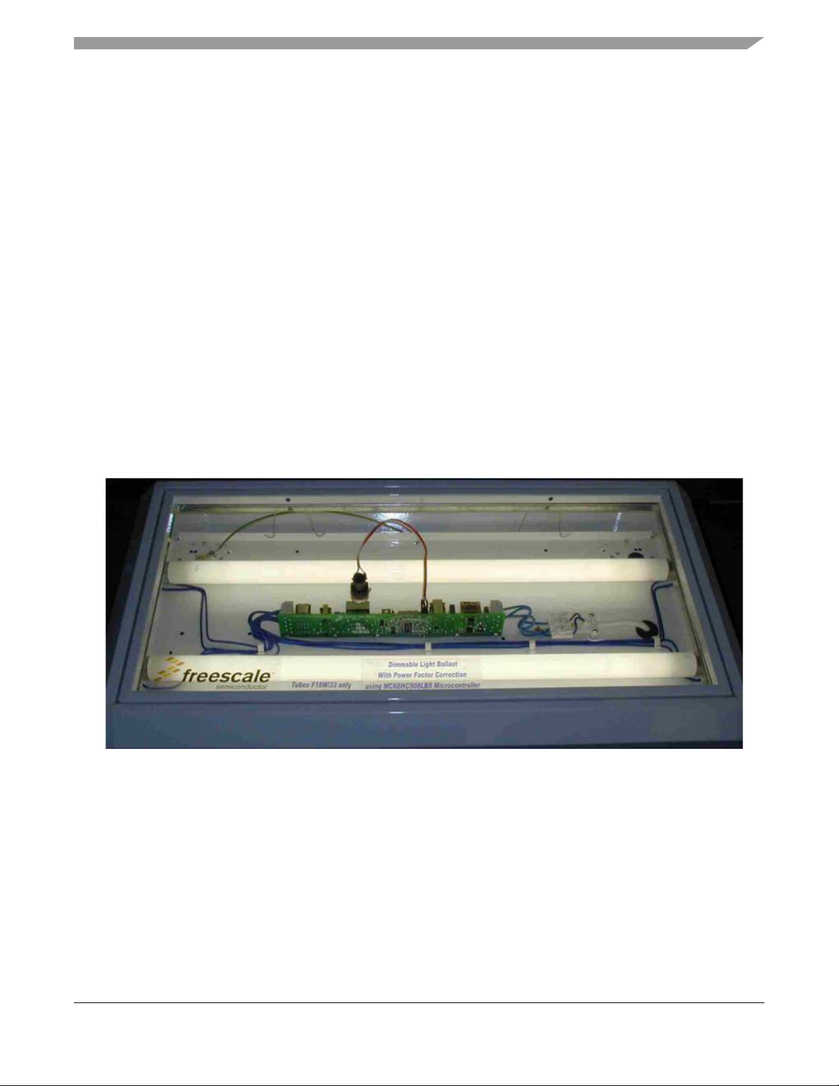
Figure 1-1. Dimmable Light Ballast with PFC Demo
1.2 Benefits of this Solution
Microcontrollers offer the advantages of low cost and attractive digital light ballast design. Using a
dedicated on-chip high resolution PWM (HRP) allows easy implementation of dimming features. PFC
improves the efficiency of the light ballast. Harmonic content of the input current for the mains supplied
equipment meets the European regulation
The advantages of the presented digital solution over standard analog solutions can be summarized as
follows:
Dimmable Light Ballast with Power Factor Correction, Rev. 1
Freescale Semiconductor 7
EN 61000-3-2 and the international standard IEC 1000-3-2.
Page 8

Introduction
• Energy saving
• Ease of adapting software for different lamps
• Ease of re-programming the system behavior
• Software can simplify the hardware
• Diagnostic functions — fault state, tube end-of-life, ignition fault, tube removed
• Open to innovation
The MC68HC908LB8 is designed for light ballast applications. It contains a HRP that is assigned to
control a lamp ballast circuit using half-bridge topology. The HRP provides two complementary outputs
for controlling a half-bridge drive. Pulse Width Modulation (PWM) with constant duty cycle is used for light
ballast control. The HRP frequency can be adjusted easily by software in range 40
kHz to 120 kHz in 256
steps. Dimming levels down to 5% are possible.
The PFC circuit uses an on-chip comparator on the MC68HC908LB8. This peripheral simplifies the
dimming light ballast solution with PFC, since it eliminates the need of external components and thus
decreases the system cost.
The reference design is intended for all geographic regions, so 110V/60Hz and 230V/50Hz input voltage
supplies are supported.
The application can be debugged using the MON08 CYCLONE debug tool in monitor mode.
WARNING
Since the application runs at high voltage, it is dangerous to connect
development tools directly to the board. Therefore, it is recommended
to use an opto-isolation monitor mode board. This separate board
provides an opto-isolated interface for the MON08 debug tool, using
the MON08 standard connector. This allows the user to safely debug
or examine code in-circuit.
1.3 The MC68HC908LB8 Microcontroller
The MC68HC908LB8 is a member of the low-cost, high performance MC68HC08 Family of 8-bit MCUs.
All MCUs in the family use the enhanced MC68HC08 central processor unit (CPU08) and are available
with a variety of modules, memory sizes and types, and package types.
Standard features of microcontroller MC68HC908LB8 are:
•8 MHz internal bus frequency
• Trimmable internal oscillator:
–4.0 MHz internal bus operation
– 8-bit trim capability
– 25% untrimmed
–2% trimmed
• 8K bytes of 10K write/erase cycle typical on-chip in application programmable FLASH
with security option
• 128 bytes of on-chip random access memory (RAM)
(1)
memory
1. Non volatile memory that retains its data when the power is removed.
Dimmable Light Ballast with Power Factor Correction, Rev. 1
8 Freescale Semiconductor
Page 9

The MC68HC908LB8 Microcontroller
• Dual channel high resolution PWM (HRP) with deadtime insertion and shutdown input to perform
light control and dimming functions for ballasts. The outputs use frequency dithering to achieve a
3.9 ns output resolution.
• Dual channel pulse width modulator module to provide power factor correction capability
• 7-channel, 8-bit successive approximation analog-to-digital converter (ADC)
• Comparator for power factor correction capability or for general-purpose use
• 7-bit keyboard interrupt
• One 16-bit, 2-channel timer interface module with one output available on port pin (PTA6) for input
capture and PWM
• 17 general-purpose input/output (I/O) pins and one input-only pin
– Three shared with HRP module
– Three shared with PWM module
– Three shared with comparator
– Seven shared with ADC module (AD[0:6])
– One shared with timer channel 0
– Two shared with OSC1 and OSC2
– One shared with reset
– Seven shared with keyboard interrupt
– One input-only pin shared with external interrupt (IRQ)
• Available packages:
– 20-pin small outline integrated chip (SOIC) package
– 20-pin plastic dual in-line package (PDIP)
• On-chip programming firmware for use with host personal computer which does not require high
voltage for entry
• System protection features:
– Optional computer operating properly (COP) reset
– Low-voltage reset
– Illegal opcode detection with reset
– Illegal address detection with reset
• Low-power design; fully static with stop and wait modes
• Standard low-power modes of operation:
– Wait mode
– Stop mode
• Master reset pin and power-on reset (POR)
• 674 bytes of FLASH programming routines in read-only memory (ROM)
• Break module (BRK) to allow single breakpoint setting during in-circuit debugging
• Internal pullup on RST pin to reduce customer system cost
• Selectable pullups on ports A and C
– Selection on an individual port bit basis
– During output mode, pullups are disengaged
• High current 10 mA sink / 10 mA source capability on all port pins
Dimmable Light Ballast with Power Factor Correction, Rev. 1
Freescale Semiconductor 9
Page 10

Introduction
Dimmable Light Ballast with Power Factor Correction, Rev. 1
10 Freescale Semiconductor
Page 11

Chapter 2 Control Theory
2.1 Introduction
This chapter covers fluorescent lamp theory and two PFC concepts - discontinuous conduction mode and
hysteresis current control mode.
2.1.1 Fluorescent Lamp Control Theory
To light a low-pressure fluorescent lamp, the electronic circuit must perform the following four main
functions:
• Provide a startup voltage across the electrodes of the lamp
• Maintain a constant current when the lamp is operating in the steady state
• Ensure that the circuit will remain stable, even under fault conditions
• Comply with the applicable domestic and international regulations (PFC, THD and safety)
Most generally, light ballast topology fairly closely matches target lamps in terms of tube wattage, length,
and diameter. The digital electronic lamp ballast includes also additional features like dimming capability,
tube end-of-life, startup fault, tube removed indication, and so on. Different tubes require different
software settings; also, some hardware components may have to be adapted accordingly.
2.1.2 Fluorescent Lamp Operation
When the lamp is off, no current flows through the tubes, and the apparent impedance is nearly infinite.
When the voltage across the electrodes reaches the V
an arc is generated across the two terminals of the lamp. This behavior is depicted by the typical operating
curve shown in
Figure 2-1.
value, the gas mixture is highly ionized and
strike
Dimmable Light Ballast with Power Factor Correction, Rev. 1
Freescale Semiconductor 11
Page 12
Control Theory
Figure 2-1. Typical Low Pressure Fluorescent Tube I/V Characteristic
The value of V
is a function of several parameters:
strike
• Gas filling mixture
• Gas pressure and temperature
• Tube length
• Tube diameter
• Temperature of electrodes: cold or hot
Typically, values of V
to the on-state voltage (V
the tube. Typically, V
are in range 500 V to 1200 V. Once the tube is on, the voltage across it drops
strike
, the magnitude of this voltage being dependent upon the characteristics of
on)
is in range 40 V to 110 V.
on
The value of Von will vary during the operation of the lamp but, in order to simplify the analysis, we will
assume, as a first approximation, that the on-state voltage is constant when the tube is running in steady
state.
Consequently, the equivalent steady state circuit can be described by two back-to-back Zener diodes as
shown in
Figure 2-2. The startup network is far more complex, particularly during ionization of the gas.
This is a consequence of the negative impedance exhibited by the lamp when the voltage across its
electrodes collapses from V
strike
to Von.
Dimmable Light Ballast with Power Factor Correction, Rev. 1
12 Freescale Semiconductor
Page 13
Introduction
Figure 2-2. Typical Fluorescent Tube Equivalent Circuit in Steady State
Up to now, there is no model available to describe the start up sequence of these lamps. However, since
most of the phenomena are dependent upon the steady state characteristics of the lamp, one can simplify
the analysis by assuming that the passive networks control the electrical behavior of the circuit. This
assumption is wrong during the time elapsed from V
to Von, but since this time interval is very short,
strike
the results given by the proposed simple model are accurate enough to design the converter. When a
fluorescent tube is aging, its electrical characteristics degrade from the original values, yielding less light
for the same input power, and different V
and Von voltages. A simple, low-cost electronic lamp ballast
strike
cannot optimize the overall efficiency throughout the lifetime of the tube, but the circuit must be designed
to guarantee the operation of the lamp even under worst case “end of life” conditions. As a consequence,
the converter will be slightly oversized to make sure that, after 8000 hours of operation, the system will
still drive the fluorescent tube.
2.1.3 Controlling the Fluorescent Lamp
As already stated, both the voltage and the current must be accurately controlled to make sure that a
given fluorescent lamp operates within its specifications.
The most commonly used network is built around a large inductor, connected in series with the lamp, and
associated with a bimetallic switch generally named “the starter”.
schematic diagram for the standard, line operated, fluorescent tube control.
Figure 2-3. Standard Ballast Circuit for Fluorescent Tube
Figure 2-3 gives the typical electrical
Dimmable Light Ballast with Power Factor Correction, Rev. 1
Freescale Semiconductor 13
Page 14

Control Theory
The operation of a fluorescent tube requires several components around the tube, as shown in Figure 2-3.
The gas mixture enclosed in the tube is ionized by means of a high voltage pulse applied between the
two electrodes.
To make this startup easy, the electrodes are actually made of filaments that are heated during the tube
ionization startup (i.e. increasing the electron emission), their disconnection being automatic when the
tube goes into the steady state mode. At this time, the tube impedance decreases toward its minimum
value (depending upon the tube internal characteristics), the current in the circuit being limited by the
inductance L in series with the power line. The starting element, commonly named “starter”, is an
essential part to ignite the fluorescent tube. It is made of a bimetallic contact, enclosed in a glass envelope
filled with a neon based gas mixture, and is normally in the OPEN state. When the line voltage is applied
to the circuit, the fluorescent tube exhibits a high impedance, allowing the voltage across the “starter” to
be high enough to ionize the neon mixture. The bimetallic contact gets hot, turning ON the contacts which,
in turn, will immediately de-ionize the “starter”. Therefore, the current can flow in the circuit, heating up
the two filaments. When the bimetallic contact cools down, the electrical circuit is rapidly opened, giving
a current variation in the inductance L which, in turn, generates an over-voltage according to Lenz’s law.
Since there is no synchronization with the line frequency (the switch operates on a random basis), the
circuit opens at a current level anywhere between maximum and zero.
If the voltage pulse is too low, the tube does not turn on, and the startup sequence is automatically
repeated until the fluorescent tube ionizes. At that time, the tube impedance falls to its minimum value,
yielding a low voltage drop across its end electrodes and, hence, across the switch. Since the starter can
no longer be ionized, the electrical network of the filaments remains open until the next turning on of the
circuit.
We must point out that the fluorescent tube turns off when the current is zero; this is the source of the
Hz flickering in a standard circuit. This is an important problem, which can lead to visual problems due
50
to the stroboscopic effect on any rotating machines or computer terminals.
To take care of this phenomena, the fluorescent tubes, at least those used in industrial plants, are always
set on a dual basis in a single light spreader, and are fed from two different phases (real or virtual via a
capacitor) in order to eliminate the flickering.
On the other hand, the magnetic ballast provides a very low cost solution for driving a low pressure
fluorescent tube. To overcome the flickering phenomenon and the poor startup behavior, the engineers
have endeavored to design electronic circuits to control the lamp operation at a much higher frequency.
The efficiency (Pin/Lux) of the fluorescent lamp increases significantly, as soon as the current through the
lamp runs above a few kilo Hertz.
The electronic circuits that can be used to build a fluorescent lamp controller can be divided into two main
groups:
• Single switch topology, with unipolar AC current, (unless the circuit operates in the parallel
resonant mode)
• Dual switch circuit, with a bipolar AC output current
Manufacturers of fluorescent lamps usually recommend operating the tubes with a bipolar AC current.
This avoids constantly biasing the electrodes as an anode-cathode pair, which, in turn, decreases the
expected lifetime of the lamp. In fact, when a unipolar AC current flows into the tube, the electrodes
behave like a diode and the material of the cathode side is absorbed by the electron flow, yielding a rapid
wear out of the filaments. As a consequence, all of the line operated electronic lamp ballasts are designed
with either a dual switch circuit (the only one used in Europe), or a single switch, parallel resonant
configuration (mainly used in countries with 110
V lines), providing an AC current to the tubes. A few low
Dimmable Light Ballast with Power Factor Correction, Rev. 1
14 Freescale Semiconductor
Page 15

PFC Control Theory
power, battery operated fluorescent tubes are driven with a single switch fly-back topology, but, the output
transformer is coupled to the tube by a capacitive network and the current through the lamp is alternating
current. However, the filaments (if any) cannot be automatically turned off by this simple configuration and
the global efficiency is downgraded accordingly.
Dual switch circuits are divided into two main topologies:
• Half-bridge, series resonant
• Current fed push-pull converter
The half-bridge is, by far, the most widely used in Europe (100% of the so-called “energy saving” lamps
and industrial applications are based on this topology), while the push-pull is the preferred solution in the
USA with around 80% of the electronic lamp ballasts using this scheme today.
Both of these topologies have their advantages and drawbacks, the consequence for the associated
power transistors being not at all negligible, as shown by
Table 2-1. The half-bridge topology controlled
by the dedicated MC68HC908LB8 MCU is implemented in Chapter 3. For more details about electronic
lamp ballast theory see Reference [1.].
Table 2-1. Main Characteristics of the Dual Switch Topologies
Parameters Half-bridge Push-pull
V(BR)CER 700 V
Inrush Current 3 to 4 times I nom
tsi window 2.6 – 3.6 µs 1.9 – 2.3 µs
Drive High and Low side Low side only
Intrinsic Galvanic Isolation no yes
NOTES:
1. These numbers are typical for operation on a 230 V supply.
2. I nom is the current into the transistors in steady state.
(1)
(2)
2 to 3 times I nom
1100 - 1600 V
(1)
(2)
2.2 PFC Control Theory
2.2.1 Introduction
The most practical electronic systems contain a conventional single-phase full-bridge rectifier and an
input filter capacitor. It is well known that this type of circuit draws high current peaks from the power line
and produces a high level of harmonics. High total harmonic distortion (THD) and low power factor
therefore reduce the maximum power available from the mains and the efficiency of the electricity supply
networks. The European Normative EN 61000-3-2 defines the limits of the harmonic content of the input
current for mains supplied equipment.To meet the norms, new designs require an active PFC at the input.
Many specific integrated circuit devices (ICs) are available on the market to perform power factor
correction. This approach requires additional electronic components, which increases the system cost
and complexity. On the other hand, there is a way to implement PFC control using the MCU, in addition
to the MCU’s main control tasks, such as motor control. Digital PFC allows missing out these specific ICs,
thereby reducing the system cost. Another benefit of the software implementation is the potential for easy
modifications without changing the hardware.
Two power factor correction approaches were implemented in this design, discontinuous conduction
mode and hysteresis current control mode. Each of these topologies has advantages and drawbacks.
Both topologies are described in the following.
Dimmable Light Ballast with Power Factor Correction, Rev. 1
Freescale Semiconductor 15
Page 16
Control Theory
2.2.2 Digital Power Factor Concept — Hysteresis Current Control Mode
The control technique is based on hysteretic current control. The system operates in continuous
conduction mode with variable switching frequency (30–100 kHz) (see
This PFC concept is designed to have the minimum of MCU performance requirements. The basic
principles of the scheme are depicted in
Figure 2-4. The PFC control algorithm includes two control loops,
a fast one for input current control and a slow one for output voltage control. The output voltage controller
is implemented digitally using the MCU. A value proportional to the required input current is modulated by
the PWM and is taken as an input to the current control loop, which is realized by the analogue
comparator. The comparator switches the MOSFET in order to maintain the required current value.
The desired shape of the input current is a sine wave. The generated current waveform is shown in
Figure 2-8.
A hysteresis current control mode PFC concept has several drawbacks, including variable MOSFET
switching frequency, non sinusoidal input current waveform and switching under current, which causes
higher losses than other PFC topologies.
The input current harmonics content, however, complies with EN 61000-3-2 standard.
The advantages are simple control circuit, low MCU resources consumption, continuous conduction
mode operation, and low total harmonic distortion (THD).
Figure 2-5).
AC Line Voltage
AC Line Current
0
L
DC Bus
MCU
ADC
Voltage
PWM
Reference
Voltage
Comparator
+
-
Actual
Current
Current Sensing
AC
LINE
AC
DC
Zero
Crossing
IC
Figure 2-4. Hysteresis Current Control Mode Principle
+ DC BUS
MOSFET
+
GND
Dimmable Light Ballast with Power Factor Correction, Rev. 1
16 Freescale Semiconductor
Page 17
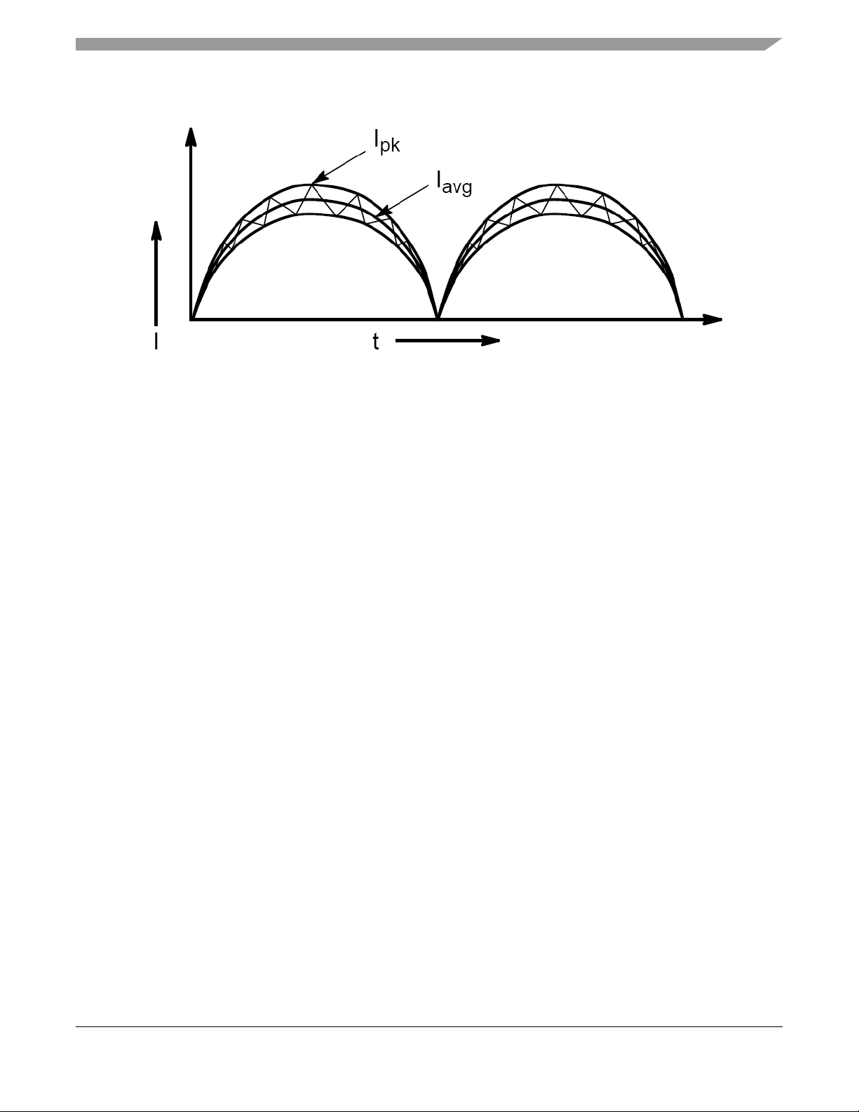
Figure 2-5. Hysteresis Current Control Mode Current Waveform
2.2.3 Digital Power Factor Concept — Discontinuous Conduction Mode
PFC Control Theory
The control technique is based on discontinuous conduction mode with a current loop with a constant
switching frequency (40 kHz) (see
Figure 2-7).
The basic principles of the scheme are depicted in Figure 2-6. The PFC control algorithm includes two
control loops, the same as the previous approach. The output voltage controller is implemented digitally
using the MCU. A value proportional to the required input current is modulated by the PWM0 and is taken
as an input to the current control loop, which is realized by the analog comparator. The comparator output
is connected to the PWM fault pin that disables the PWM output. PWM1 is used directly for switching the
MOSFET in order to maintain the required current value. PWM1 is switched off in every period where the
reference sine wave signal generated by PWM0 is higher than the actual current sensed signal on the
shunt resistor.
The desired shape of the input current is a sine wave. The generated current waveform is shown in
Figure 2-8.
The discontinuous conduction mode PFC concept has several drawbacks — higher THD than hysteresis
current control mode, non sinusoidal input current waveform, and the discontinuous conduction mode
itself. The input current harmonics content, however, complies with EN 61000-3-2 standard.
The advantages are a simple control circuit, with low MCU resource consumption, and low losses.
Dimmable Light Ballast with Power Factor Correction, Rev. 1
Freescale Semiconductor 17
Page 18
Control Theory
DC Bus
Voltage
L
AC
LINE
Reference
AC
DC
Zero
Crossing
ADC
IC
MCU
PWM
FAULT
PIN
Voltage
PWM0
PWM1
Actual
Current
Comparator
+
-
MOSFET
Current Sensing
Figure 2-6. Discontinuous Conduction Mode Principle
+ DC BUS
+
GND
Figure 2-7. Discontinuous Conduction Mode Current Waveform
Dimmable Light Ballast with Power Factor Correction, Rev. 1
18 Freescale Semiconductor
Page 19
Figure 2-8. Generated Input Current Waveform
2.2.4 Concept Summary
PFC Control Theory
Both the PFC solutions can be used for applications that do not require a large portion of the MCU’s
resources, because they consume only a fraction of the MCU performance. Compared to a dedicated IC
solution, digital PFC offers high flexibility and cost reduction in the overall design, as the PFC function can
be provided within the MCU capability of the main application. Digital PFC also provides additional
benefits such as a wide range of input voltages (85
V to 265 V AC) at a constant output DC voltage.
However, hysteresis current control mode is more suitable for power above 100W, and discontinuous
conduction mode for low power consumption.
Dimmable Light Ballast with Power Factor Correction, Rev. 1
Freescale Semiconductor 19
Page 20

Control Theory
Dimmable Light Ballast with Power Factor Correction, Rev. 1
20 Freescale Semiconductor
Page 21

Chapter 3 Reference Design
3.1 Application Outline
The presented system is designed to control two parallel connected fluorescent lamps. The reference
design meets the following performance specification:
• Single board solution with MC68HC908LB8 microcontroller
• Supported power supply: 110V/60Hz and 230V/50Hz
•Low THD
• High power factor achieved using the PFC circuit
• Control techniques incorporating:
– Preheating
–Strike
– Run mode
• User interface (dimming level potentiometer, monitor mode interface)
• Flickering effect removal
• Lamp aging recognition
• Fault detection
– DC-bus under-voltage detection (software)
– DC-bus over-voltage detection (software)
– Ignition fault (software)
– Zero current fault (software)
3.2 Dimmable Light Ballast Characteristics
Table 3-1 provides the basic characteristics of the Dimmable Light Ballast Demo with PFC at 25°C and
400 V DC-bus voltage.
Dimmable Light Ballast with Power Factor Correction, Rev. 1
Freescale Semiconductor 21
Page 22

Reference Design
Table 3-1. Light Ballast Characteristics
Parameter Unit Value
Lamp Type F18W/33
Input Power W 8...31
Input Current
(230VAC)
Preheat Output
Frequency
Preheat Output
Volt age
Preheat Time ms 900
Running Output
Frequency Range
Running Output
Voltage Range
Input AC Voltage VAC 110V/60Hz, 230/50Hz
Ambient
Temperature Range
Power Factor 0.94...0.99
Total Harmonic
Distortion
Output Ignition
Volt age
mA 40...290
kHz 86
Vpp 345
kHz 50...100
V 200...235
°C 0.50
% 5.2...24.6
Vpp 510
3.3 Application Description
The system concept is shown in Figure 3-1. The system consists of:
• Control board with MC68HC908LB8 microcontroller
• Two fluorescent lamps
The MC68HC908LB8 MCU runs the main control algorithm. According to the dimming level potentiometer
It generates output signals for the half-bridge inverter which controls the ballast circuit. It also controls
PFC. The desired dimming value is set by the potentiometer, because the human eye is more sensitive
at lower light levels. The input values from the potentiometer are converted using brightness linearization.
The HRP uses a frequency control method for dimming. It incorporates hardware that allows dithering
between two adjacent frequencies for smooth light level dimming.
Dimmable Light Ballast with Power Factor Correction, Rev. 1
22 Freescale Semiconductor
Page 23

MAINS
MAINS
FILTER RECTIFIER
FILTER RECTIFIER
FILTER RECTIFIER
CROSSING
CROSSING
ZERO
ZERO
CONTROL BOARD
CONTROL BOARD
USER INTERFACE
USER INTERFACE
MONITOR
MONITOR
MODE
MODE
LUMINANCE
LUMINANCE
LEVEL
LEVEL
U
U
REQ
REQ
BUS VOLTAGE
BUS VOLTAGE
DC-
DC-
-
-
e
e
BRIGHTNESS
BRIGHTNESS
LINEARIZATION
LINEARIZATION
DRIVER
DRIVER
DRIVER
ACTUAL CURRENT
ACTUAL CURRENT
PWM
PWM
GENERATION
GENERATION
sineGain
sineGain
PI
PI
REGULATOR
REGULATOR
DC-BUS
DC-BUS
PFC
PFC
PFC
PWM
PWM
FILTER
FILTER
+
+
e
e
i
i
req
req
MC68HC908LB8
MC68HC908LB8
POWER
POWER
POWER
SUPPLY
SUPPLY
SUPPLY
-
-
-
-
DRIVER
DRIVER
PWM
PWM
HIGH
HIGH
RESOLUTION
RESOLUTION
PWM
PWM
f
f
PI
PI
REGULATOR
REGULATOR
i
i
act
act
Application Description
RESONANT
RESONANT
RESONANT
CIRCUIT
CIRCUIT
CIRCUIT
HALF BRIDGE
HALF BRIDGE
HALF BRIDGE
DIFFERENTIAL
DIFFERENTIAL
DIFFERENTIAL
VOLTAGE
VOLTAGE
VOLTAGE
CURRENT
CURRENT
1
1
HRP
HRP
CURRENT
CURRENT
PROCESSING
PROCESSING
e
e
TUBE 2 CURRENT
TUBE 2 CURRENT
TUBE
TUBE
FLUORESCENT LAMPS
FLUORESCENT LAMPS
Figure 3-1. Dimmable Light Ballast — System Concept
3.3.1 Light Ballast Control
The HRP provides two complementary PWM outputs for controlling a half-bridge in a light ballast
application. It uses a dithering control method to provide a high step resolution (3.9 ns) from an 8
MHz
input clock when driving inductive loads.
The High Resolution PWM Module (HRP) uses a dithering technique to increase the resolution of the
output signal.The output switches between two frequencies or duty cycles at a programmable rate. By
varying the percentage of time spent on each frequency/duty cycle, the output will appear to be at a value
between the two dithering frequencies/duty cycles when driving an inductive load.
The advantage is easy implementation of a control method for half-bridge inverter using few external
devices. The main advantage is simple performance using few instructions to perform the dithering
control algorithm.
3.3.2 Power Factor Correction
The power factor correction circuitry provides the “sinusoidal” input current by controlling the PFC switch.
In the control loop, the actual DC-bus voltage is compared with the desired one. The control error is
processed by the PI (proportional-integral) controller, which generates the amplitude of the input
“sinusoidal” current. The PWM generator generates the desired sinusoidal current profile using a PWM
technique. The digital output signal is filtered by a passive filter and the resulting analog waveform is
compared with the actual input current by an on-chip comparator. The comparator output controls directly
Dimmable Light Ballast with Power Factor Correction, Rev. 1
Freescale Semiconductor 23
Page 24

Reference Design
the PFC switch in hysteresis current control mode or output is used for switch off PWM1 in DCM. Than
PWM1 signal is used directly for switching the PFC switch transistor.
3.3.3 Protection Features
During the startup phase and run phase, some erroneous states can occur. When the DC-bus voltage
does not reach the required value or is out of limits then a fault signal is generated. The DC-bus voltage
is also checked against limits in run mode. If any of the previously mentioned faults occurs, all modules
are disabled, lamps go out, and the fault diode blinks.
3.4 Software Specification
The software is written in C. The software specifications are listed in Table 3-2. A useful feature of this
application is the ability to debug software via the MON08 CYCLONE debug tool connected to JP1 header
connector. The Real-Time Debugger from Metrowerks can be used as a debug tool.
Tabl e 3-2. Software Specification
Dithering control
Control Algorithm
Target Processor MC68HC908LB8
Language C with some arithmetical functions in assembler
Compiler Metrowerks ANSI-C/C++ Compiler for HC08
MCU Oscillator Frequency 16 MHz (with default software setting)
MCU Bus Frequency 4 MHz (with default software setting)
Targeted Hardware Dimmable Light Ballast With PFC Demo Board
Current loop control
Voltage loop control
A detailed description of how to set Debugger for commutation with MON08 CYCLONE is given in
Reference [
2]. For safe debugging it is recommended use an opto-isolation board connected between the
MON08 CYCLONE and the Light Ballast Demo Board. The Opto-isolation Board user manual can be
found in Reference [
3].
3.5 Hardware Specification
The other system specifications are determined by the target hardware and lamp characteristics. The
board and its connections are shown in
This hardware set is designed for fluorescent lamp and mains voltage. The specifications for a high
voltage hardware and fluorescent lamp set are listed in
and 110 VAC mains.
Chapter 4 Hardware Design.
Table 3-1. The hardware operates on 230 VAC
Dimmable Light Ballast with Power Factor Correction, Rev. 1
24 Freescale Semiconductor
Page 25

Chapter 4 Hardware Design
4.1 Hardware Implementation
This chapter covers the system hardware implementation. The dimmable light ballast board is shown in
Figure 4-1.
Figure 4-1. Dimmable Light Ballast - Demo Board
4.2 System Modules
The light ballast system hardware is shown in the block diagram in Figure 4-2. It incorporates the
controller board, powered from AC line and fluorescent tubes. As can be seen, the controller board
contains four major parts:
• Input and PFC (Input EMI Filter, Bridge Rectifier, Boost topology PFC circuit, DC-bus Voltage,
DC-bus Sensing, Mains Zero Crossing Sensing, Comparator Circuit, Buffer Circuit)
• Inverter (Half-bridge Drive, Resonant Circuit, Output Inductance Circuity, Different Voltage
Sensing, Tube Currents Sensing)
• Microcontroller (MC68HC908LB8)
• Power Supply (Switch Mode Power Supply)
Detailed descriptions of the individual parts of the controller boards follows. Note that the reference design
includes the PCB design files and bill of materials (BOM).
Dimmable Light Ballast with Power Factor Correction, Rev. 1
Freescale Semiconductor 25
Page 26

Hardware Design
Figure 4-2. Dimmable Light Ballast with Hysteresis PFC HW variation — Hardware Block Diagram
4.2.1 Input and PFC
The input and the PFC part provide the DC-bus voltage to supply the inverter. The schematic for
hysteresis current control mode is shown in
against hysteresis mode is that the gate of Q4 is connected to pin PWM1 of the MCU (see Figure A-2),
not to the output of the comparator. The input stage consists of an EMI filter and a single-phase full-bridge
rectifier. Although the PFC regulator is called an active filter, it does not suppress all harmonics. For this
reason, the EMI filter is placed at the input.
The PFC is based on the most popular non transformer isolated DC-DC boost (step-up) converter
topology. The PFC stage is built with input inductor L1, power MOSFET switch Q1, output rectifier diode
D1, and output capacitor C4. Capacitor C3 performs a filtering function. The input stage converts the
mains AC voltage, rectified by the diode bridge U1, to an output DC voltage on the output capacitor C4.
The current flowing through inductor L1 is sensed by the current sense resistor R4. There are two different
values of resistor R4, 1.5
Ω for rectified input voltage lower than half of DC-Bus voltage and 2.7Ω for higher
voltage. The voltage drop over the current sense resistor corresponds to the measured current. The
circuit, with resistors R3, R5, R7, R9, diodes D2 and D15, and capacitor C27 works as a mains
zero-crossing detector. It senses rectified mains voltage and generates zero-crossing pulses with an
amplitude of 5
volts. With the help of this detector, the microcontroller synchronizes its operation with the
mains frequency.
The DC-bus voltage sensor consists of resistors R1, R2, R6, and R8. It senses the output voltage of the
PFC, and its output is connected to the MCU AD converter. In hysteresis current control mode the output
Figure 4-3. The difference in discontinuous conduction mode
Dimmable Light Ballast with Power Factor Correction, Rev. 1
26 Freescale Semiconductor
Page 27

System Modules
signal of the comparator (Comp Out) controls the power switch Q1 through the output buffer, which
consists of transistors Q2, Q3, and Q4, resistors R10, R13, R34, R35, R36, and R37, and capacitor C7.
For discontinuous conduction mode the comparator output is disconnected from the Q4 transistor gate.
The PWM1 pin is connected to the Q4 transistor gate.
Digital PFC is driven by the MCU. The MC68HC908LB8 peripherals used for PFC are listed below:
• AD converter — channels ADC1 and ADC2
• PWM0 for generating sine wave
• comparator
• IRQ pin for zero-crossing detection
The PFC control algorithm
• converts the sensed output voltage to a digital value
• provides software PI regulator for a voltage feedback loop
• programs its PWM channel to create the pattern of the input current
• synchronizes operation with the mains frequency using mains zero-crossing detection
The control algorithm is described in 5.2 Control Algorithm Description.
DC-BUS VOLTAGE OUTPUT AND SENSING
J1
J1
PM100-INP_CONN-6
PM100-INP_CONN-6
6
6
I6
I6
5
5
I5
I5
4
4
NC
NC
3
3
I3
I3
2
2
I2
I2
1
1
I1
I1
PFC Current Sense
PFC Current Sense
INPUT EMI FILTER AND BRIDGE RECTIFIER
1 4
C1
C1
10nF 275V X2
10nF 275V X2
R14
R14
2K0
2K0
1 4
2 3
2 3
GND
GND
1
1
2
2
GND
GND
12
12
1 2
1 2
C5
C5
4n7 250/1000V Y2
4n7 250/1000V Y2
L6
L6
CMFIL2
CMFIL2
R11
R11
3K0
3K0
C8
C8
82pF
82pF
12
12
RV1
RV1
275V
275V
Comp -
COMPARATOR CIRCUIT
5V
5V
GND
GND
2.7mH
2.7mH
L1B
L1B
PFCIND3
DF1510S
4
4
AC2
AC2
3
3
AC1
AC1
12
12
R3
R3
220K
220K
1
1
R5
R5
220K
220K
2
2
1
1
R7
R7
220K
220K
2
2
C10
C10
220nF
220nF
Comp Out
150nF 275V X2
150nF 275V X2
1
1
DC+
DC+
2
2
DC-
DC-
MAINS ZERO CROSSING SENSING
12
D15
D15
R9
BAT48
BAT48
47K
GND
D2
D2
BZV55C5V6
BZV55C5V6
GND
GND
1
1
R12
R12
10K
10K
2
2
C2
U1
C2
U1
DF1510S
PFCIND3
12
12
PFC Gate
PFC Gate
1 2
1 2
R4 2R7
R4 2R7
PFC Current Sense
PFC Current Sense
Zero Detect
Zero Detect
C27
1n5
GND
C7
C7
12
12
100nF
100nF
R10
R10
6K8
6K8
GND
GND
BEQ2
BEQ2
R13
R13
620R
620R
BCQ3
BCQ3
D
G
Q4
MMBF0201
S
GND
BOOST CONVER TER
D1
D1
53
53
MURS160T3
MURS160T3
D
D
G
G
S
S
15V
15V
12
12
R35
R35
0R
0R
1
1
R34
R34
0R
0R
2
2
C
C
BC846B
BC846B
E
E
BC856B
BC856B
GND
GND
Q1
Q1
IRF820A
IRF820A
R36
R36
0R
0R
PFC Gate
PFC Gate
BUFFER CIRCUIT
10nF 630V TC356
10nF 630V TC356
R37
R37
12
12
C3
C3
0R
0R
15V/1
15V/1
GND
GND
+
+
C4
C4
22uF 450V
22uF 450V
C6
100nF
12
R1
560K
12
R2
560K
12
R6
510K
DCB Divider
12
R8
18K
GNDGND
DCB
DCB
1
2
CONN/HDR/2X1
GND
JP6
Figure 4-3. Dimmable Light Ballast — Input and PFC
Dimmable Light Ballast with Power Factor Correction, Rev. 1
Freescale Semiconductor 27
Page 28

Hardware Design
4.2.2 Inverter
The power inverter generates the proper voltage for the fluorescent tubes. The power inverter consists of
two MOSFET transistors driven by a half-bridge driver. It incorporates the half-bridge, a resonant circuit,
different voltage and tube current sensing, and output inductance circuity.
The half-bridge driver IR2106 from International Rectifier is electrically connected according to the
manufacturer’s recommendations. The half-bridge is supplied from the DC-bus voltage. It is controlled by
the TOP and BOT signals from the MCU.
The half-bridge lamp resonant circuit consists of capacitor C15 and inductance L7. It provides preheating,
ignition, and running operating conditions by changing the operating frequency.
The tube voltage difference circuit consist of coils L3A, L3B, and L3D, resistors R21, R24, R22, and R151,
diode D8, and capacitor C17, and is used to sensing voltage differences between lamps. It helps to
recognize aging of the lamps.
Coils L4 and L5 and diodes D4 and D5 are for filament preheating. Diodes maintain a small offset to
remove the flickering effect. Coils L3A and L3D balance possible differences in current flow into tubes,
mainly at ignition stage. Devices R19, D7, R152, D6, C16, and R20 sense the current flow in tube 1 (and
similarly for tube 2).
For different tubes parameters, the tube currents are different. The ignition circuit formed by L3D, L3A,
and R17 balance the current. The compensation current flows through R17 until the tube currents are
equal, at which time the ignition of both tubes can be done reliably.
Tubes preheating heats the tubes to the desired temperature before startup. It decreases the wear-out
and increases the life-time and reliability in startup. Also, the voltage required for ignition is smaller.
Each tube has its own preheating circuity. Tube 1 uses L4. Tube 2 uses L5. The preheating voltage and
time is set-up in software and is controlled by the TOP and BOT signals from the HRP.
The flickering effect is caused by reducing the voltage to zero during the light ballast operation. To avoid
this, the Zener diodes D4 and D5 maintain a small voltage on both tubes at all times.
The output inductance circuity performs several important functions in the light ballast application. It helps
to ignite lamps, when tube parameters differ (due, for example, to different aging of the lamps). It removes
the flickering effect and provides filament preheating.
Dimmable Light Ballast with Power Factor Correction, Rev. 1
28 Freescale Semiconductor
Page 29

DCB
TOP
BOT
15V/1
1 2
D3
MURA160
C13
1uF
25V
R15
IC1
1
Vcc
VB
2
HIN
HO
3
LIN
COM4LO
IR2106
Tube V o l t ag e d i f fe r e nc e
HALF BRIDGE
10R
8
7
6
Vs
5
System Modules
J2
L4C
HEAT7
43
R23
20R
0.5W
TU BE C onn ector
O11O22O33O44O55O66O77O8
6 5
L4D
L5C
HEAT7
HEAT6
R19
20R
0.5W
1 2
GND
8
56
3 4
R152
D7
MBRS140
1 2
GND
R150
0R
D10
MBRS140
TUBE CURRENTS SENSING
L5D
HEAT6
D9
BAT48
D6
BAT48
0R
C18
22nF
C16
22nF
R25
10K
Tube Current 1
R20
10K
Tube Current 2
OUTPUT INDUCTANCE CIRCUITY
C26
Q5
IRF830A
33R
C11
100nF
33R
Q6
IRF830A
D
G
S
D
G
S
GND
C17
6n8
GND
R16
R18
10nF 630V TC356
GND
RESONANT CIRCUIT
12
C28
470pF 1KV
1 3
12
C14
470pF 1KV
D8
BAT48
R22
30K
GND
L7
RES5
1mH
R151
C12
100nF 630V
1 2
12
8n2 1KV
0R
C15
GND
D4
BZG05C22
L3D DIFF8
1 8
L3A DIFF8
D5
BZG05C22
R21
3K3
R24
N/P
54
72
L3BDIFF8
2 7
L4B
HEAT7
1 2
R17 10K
L5B
HEA T6
GND
GND
27
GND
DIFFERENT VOLTAGE SENSING
Figure 4-4. Dimmable Light Ballast — Inverter
Dimmable Light Ballast with Power Factor Correction, Rev. 1
Freescale Semiconductor 29
Page 30

Hardware Design
4.2.3 Microcontroller
The MC68HC908LB8 microcontroller is the core of the application. It processes the input and feedback
signals and generates appropriate control signals. The description of the pins follows.
The inverter is controlled by signals on the TOP and BOT pins of the MCU.
Signal PWM0 is used to generate a sine wave. This signal (on comparator pin V+) is compared with the
real current (on comparator pin V-) in the on-board comparator. The real current is sensed using the shunt
resistor R4. The signal from PWM0 is filtered in the RC filter comprised of R30, R31 and capacitor C9.
The output of the comparator appears on pin VOUT.
The IRQ pin is used for the zero-crossing detection circuit and for entry to the monitor mode.
The microcontroller stage incorporates two header connectors, the Luminance Level connector and the
Monitor Mode connector. The Luminance Level connector is used for the Luminance Level potentiometer
(see
Table 4-1). The Monitor Mode connector enables the MCU to enter the Monitor Mode. For Monitor
Mode, the IRQ, OSC1, PTA0, and PTA1 pins are used (see Table 4-2).
The Fault LED is connected to pin PTA5; it indicates the actual state of the application.
DC-bus shift-down voltage is sensed on pin ADC2.
Real currents through tube1 and tube2 are sensed on pins ADC3 and ADC4. The tube voltage difference
is sensed on pin ADC5.
In the discontinuous conduction mode HW variation, PWM1 pin is used directly for switching the PFC
switch transistor (see
Figure A-5). Comparator output is internally connected to the PWM fault pin. In the
hysteresis current control mode HW variation, it is not used.
Dimmable Light Ballast with Power Factor Correction, Rev. 1
30 Freescale Semiconductor
Page 31

System Modules
TOP
BOT
Comp Comp Out
Zero Detect
R30
13K
5V
D11
R26
1K
R27
1K
R38
N/P
5V
R29
11K
R31
3K9
GND
C9
100nF
1 2
GNDGND
IC2
6
PTB0/TOP
7
PTB1/BOT
8
PTB2/FAULT
9
PTB3/PWM0
10
PTB4/PWM1
11
PTB5/V+
12
PTB6/V-
13
PTB7/VOUT/ADC6/FAULT
3
PTC0/OS C1
4
PTC1/OS C2
5
PTC2/SHTDWN/IRQ
MC68HC908LB8-CASE_751D
Serial Da ta
LED
PTA0/ADC0/KBI0
PTA1/ADC1/KBI1
PTA2/ADC2/KBI2
PTA3/ADC3/KBI3
PTA4/ADC4/KBI4
PTA5/RST/KBI5
PTA6/ADC5/TCH0/KBI6
VDD
VSS
5V
1
2
3
4
5
6
GND
CONN/HDR/6X1
JP5
R28
1K8
5V
R33
10K
R260
14
15
16
17
18
19
20
1
2
GND
0R
Serial Data
DC B Di v i d er
Tube Cur r en t 1
Tube Cur r en t 2
Tube Vol t age differe nce
C19
100nF
1 2
25V
R39
5V
1
2
3
Luminance Leve l
GND
JP2
0R
Figure 4-5. Dimmable Light Ballast — Microcontroller
NOTE
The Luminance Level potentiometer should be connected to the PCB in the
required manner. This means that if the potentiometer is in a zero position,
a 0% Luminance is required and 0V must be available on pin 2 of connector
JP2.
Table 4-1. J1 Luminance Header
Pin number Signal
1 +5V
2 PTA1
3 GND
Dimmable Light Ballast with Power Factor Correction, Rev. 1
Freescale Semiconductor 31
Page 32

Hardware Design
Table 4-2. J2 Interface Header
Pin number Signal
1 +5V
2 PTC2
3 PTC0
4 PTA0
5 GND
6 PTA1
Dimmable Light Ballast with Power Factor Correction, Rev. 1
32 Freescale Semiconductor
Page 33

System Modules
4.2.4 Power Supply
The function of the switch mode power supply (SMPS) is to feed the inverter and output buffer circuit with
V and to supply the microcontroller stage by 5 V (see Table 4-3). The SMPS is supplied from the
15
DC-bus voltage. It uses the monolithic high-voltage regulator NCP1010 from ON Semiconductor
connected as recommended by the manufacturer. It can provide 15
power supply from a 15
V source, a step-down resistor R32, 5V1 Zener diode D13, and filtering capacitor
C25 are used.
22uF
35V
C20
+
1 2
DCB
GND
IC3
1
VCC
2
FB
3
DRAIN
12
C23
+
1uF
450V
NCP1010-SOT223
1 2
1nF 25V
C24
GND
4
GND
D12
MURA160
U3
4
SFH6106
TL-RAD EZK
L8
4.7mH
1
23
D14
BZV55C13
VDC @ 100 mA. To achieve a 5 V
15V 5V
12
C21
+
100uF
35V
GND GND
C22
1uF
1 2
25V
15V/1
R32
390R
GND
D13
BZV55C5V1
GND GND
Figure 4-6. Dimmable Light Ballast — Power Supply
Table 4-3. Supplied Voltages
Volt age Supply
+15V Driving stage, Output buffer circuit
+5V Microcontroller stage
C25
220nF
1 2
Dimmable Light Ballast with Power Factor Correction, Rev. 1
Freescale Semiconductor 33
Page 34

Hardware Design
Dimmable Light Ballast with Power Factor Correction, Rev. 1
34 Freescale Semiconductor
Page 35

Chapter 5 Software Design
5.1 Introduction
This section describes software features and behavior of the software in all function modes. The software
is described in terms of:
• Control Algorithm Description
• Software Implementation
• Detailed Software Description
• Microcontroller Usage
• Constant and Variable Definitions
5.2 Control Algorithm Description
The application performs dimmable light ballast for fluorescent lamp control and PFC control. It uses
microcontroller built-in peripherals.
current control mode HW variation. Software block diagram for DCM HW variation is not placed because
diagram is very similar. As can be seen, the PFC Control and Light Ballast Control are separate routines.
Figure 5-1 shows the high level software block diagram for hysteresis
Figure 5-1. Dimmable Light Ballast with Hysteresis PFC HW Variation — Software Block Diagram
Dimmable Light Ballast with Power Factor Correction, Rev. 1
Freescale Semiconductor 35
Page 36

Software Design
5.2.1 Power Factor Correction Control
PFC control consists of DC-bus voltage control using the PI controller, phase shift synchronization,
reference sine wave generation and generation of output PFC control signals. It also includes the
trimming of the internal oscillator frequency according to the frequency of the mains provided.
5.2.1.1 DC-bus Voltage Control
The actual value of the DC-bus voltage is sensed by the AD converter. This value is compared with the
required DC-bus value. The regulation error is then the input value for the PI regulator. The output value
from the PI regulator is the reference sine wave gain. The PWM module generates a reference sine wave
with calculated amplitude. The filtered reference sine wave is compared with the actual current using the
on-chip comparator. For the hysteresis current control mode HW variation, the output from the
comparator is the switching signal for the PFC MOSFET transistor. For the discontinuous conduction
mode HW variation, the output comparator is connected to the PWM fault pin. The PWM1 signal is directly
used for switching the PFC MOSFET transistor.
5.2.1.2 Phase Shift Synchronization
Phase shift synchronization synchronizes the generated PFC reference sine wave to the frequency of the
mains. It is realized by means of:
• Zero voltage crossing detection (zero voltage sensor)
The zero voltage crossing sensor generates a falling edge every time when the input voltage
crosses zero from positive to negative polarity.
• External interrupt
An external interrupt is triggered by the zero voltage crossing sensor. The interrupt subroutine is
used to get the content of timer TIM registers TCNTH:TCNTL for automatic microcontroller
trimming and for PFC reference sine wave amplitude gain calculation in lamp run mode.
• MCU oscillator frequency trimming
For microcontroller automatic trimming, the timer TIM is used as an interval counter. The timer is
incremented by the internal clock (divided by prescaler). Its content is cleared every
produced by the voltage zero crossing sensor. A user defined value determines what number
should be found in TIM registers TCNTH:TCNTL. On the basis of the comparison between required
and actual counter values, the content of the oscillator trim register OSCTRIM is adjusted with
ramp.
IRQ interrupt
5.2.1.3 Reference Sine Wave Generation
Reference is performed by the PWM peripheral. The software contains a sine wave table with values for
interval and maximum amplitude. The amplitude of the sine wave depends on the value of the DC-bus
voltage and it is adjusted by the PI controller every 20ms. Two different sets of PI controller parameters
are used, one for MCU startup, when the DC-bus voltage must reach the required value quickly and HRP
is not activated, and the second during standard running operation.
5.2.1.4 Generation of Output PFC Control SIgnal
The generated output PFC signal controls the PFC power MOSFET. An on-chip operational amplifier is
used in comparator mode. It compares the reference sine wave, filtered by the RC filter, with the actual
current and generates a switching signal for the PFC MOSFET transistor in the hysteresis current control
mode HW variation. In discontinuous conduction mode comparator output is used for switching off the
PWM1 signal. It works as a fault detection in fact. When the actual current sensed on the shunt resistor
Dimmable Light Ballast with Power Factor Correction, Rev. 1
36 Freescale Semiconductor
Page 37

Control Algorithm Description
is higher than the generated sine waveform, then the comparator output is in log.1 and PWM1 is switched
off. This happens every PWM period and this process is called cycle by cycle limiting. PWM1 operates at
a 40 kHz frequency with variable duty cycle. For safety reasons, the comparator is enabled when the
microcontroller is initialized and mains voltage synchronization is provided.
5.2.2 Light Ballast Control
Light Ballast Control controls the fluorescent tubes. The control process consists of two parts (modes),
tube start mode and tube run mode.
and run mode.
Figure 5-2 shows the software control time diagram during start mode
Figure 5-2. Dimmable Light Ballast — Control Time Diagram
5.2.2.1 Tube Start Mode
When the DC-bus voltage reaches the required value, the HRP is enabled at maximum ballast frequency
and kept for a set time. Then the ballast frequency is ramped down to the preheat frequency and kept for
a set time. This procedure preheats the filaments. In the next stage, the ballast frequency is ramped down
until the lamps are ignited. During the lamp ignition procedure, the frequency and tube currents are
controlled (see Reference [
4]).
5.2.2.2 Luminance Level Control (Tube Run Mode)
Luminance Level Control is active after tube ignition. The actual values of the tube currents are sensed
by the AD converter. Average value of currents is compared with required current value after luminance
Dimmable Light Ballast with Power Factor Correction, Rev. 1
Freescale Semiconductor 37
Page 38

Software Design
level adjustment (brightness linearization). The regulation error is then the input value for the PI regulator.
The output value from the PI regulator is the HRP period for half bridge power stage.
Input required luminance level adjustment adapts the required luminance level to its exponential value.
This is done because of the nonlinear function dependence of luminance on the lamp current. The
transformation table is used. The table contains the required current values.
The values in the table can be calculated using the following expression.
ki
⋅
i
req
where:
•i
•i
• A is the exponential curve gain
• q is the exponential curve offset
To calculate the coefficients A and q correctly, the following values must be known.
• Minimum HRP frequency f
• Maximum HRP frequency f
• Tube current measurement range i
• Minimum required tube current i
• Maximum required tube current i
• ADC maximum value AD
• ADC minimum value AD
• Minimum required tube current value converted to ADC range i
• Maximum required tube current value converted to ADC range i
• k determines function precision
is the required current in the exponential expression used for the control algorithm calculation
reg
is the required current measured by the AD converter
regAD
Ae
reqAD
q+⋅= (EQ 5-1)
min
max
max
t
min
tmax
max
min
tADmin
tADmin
Then:
i
tADmin
i
tADmax
This is a time-consuming calculation, but it can be simplified by using the sheet “HRP_Setup” provided in
the Excel file “DLB_Setup.xls”. This file can be downloaded along with this designer reference manual.
Dimmable Light Ballast with Power Factor Correction, Rev. 1
round i
round i
i
A
----------------------------------------------------=
kAD
e
qi
tADmin
tmin
tmax
tADmaxitADmin
⋅
max
AD
AD
–
kAD
e
–
kAD
Ae
⋅–=
maximax
maximax
⋅
min
⋅
⁄ 0;⋅()=
min
(EQ 5-2)
⁄ 0;⋅()=
(EQ 5-3)
(EQ 5-4)
(EQ 5-5)
38 Freescale Semiconductor
Page 39

Software Implementation
5.3 Software Implementation
The general software implementation is illustrated in Figure 5-3. It incorporates the main routine entered
from Reset and three interrupt states. The main routine includes the initialization of the microcontroller
including PWM, HRP, ADC, and pins used in the application, and sets initial values for the PI regulator.
The infinite loop is performed as long as board remains connected to the mains and no fault conditions
are detected.
The interrupt states provide for trimming the internal oscillator, mains synchronization, reference sine
wave generation, and fault detection and processing.
OverFlow Interrupt
of Timer, Fault
Interrupt
Fault
Interrupt
Routine
done
RESET
PWM Reload Inte rrupt
done
IRQ Interrupt
done
Sinewave
Generation
Interrupt
Routine
Synchronization
Interrupt
Routine
MCU & Application
Initialization
done
Main
Infinite
Loop
Figure 5-3. Software Implementation
5.3.1 Initialization Setup
Prior to running the main program loop, the initialization setup sets the microcontroller operation mode
and peripherals. The quickest way to set and PWM is to use the auxiliary Excel sheet Reference [
achieve the required system behavior and communication with peripherals, the following registers and
initial values are set.
• Set configuration registers CONFIG1 and CONFIG2 at the beginning of the initialization; they can
be written once only after each reset.
The register CONFIG1 sets:
– long COP time-out period
– enable LVI module
– disable STOP instruction
4]. To
Dimmable Light Ballast with Power Factor Correction, Rev. 1
Freescale Semiconductor 39
Page 40

Software Design
The register CONFIG2 sets:
– internal oscillator
– IRQ interrupt enabled
– IRQPUD must be 0 to connect the internal pullup resistor between IRQ pin and Vdd.
• IRQ status and control register INTSCR sets:
– IMASK enable IRQ interrupt requests
– IRQ interrupt on falling edge only
• Analog to digital converter clock register (ADCLK)
– sets the ADC clock. ADC clock = bus clock / prescaler. The recommended value for the ADC
clock is 1
MHz.
• PWM setup — void Set_PWM(void)
The subroutine initializes PWM values, and sets 0% duty cycle on PWM.
For a better understanding of PWM setup and logic, see 5.3.1.1 PWM Setup.
• HRP setup — void Set_HRP(void)
The subroutine initializes and sets HRP registers. For a better understanding of HRP setup and
logic, see
5.3.1.2 HRP Setup.
5.3.1.1 PWM Setup
The PWM module can generate two independent PWM signals used for PFC control. These signals are
edge-aligned. PWM resolution is one clock period which is dependent on the internal bus frequency
(BUSCLK) and a programmable prescaler (PRSC0, PRSC1). Also, programmable fault protection and
PWM signal polarity controls are provided.
For the application, the PWM is set to 40 kHz, resulting in 101 levels of PWM0 at a 4 MHz bus frequency.
Because of the hardware configuration, negative polarity control of the PWM output is required.
For proper operation of the PWM module, the following registers must be set:
• PWM counter modulus registers PMODH and PMODL hold a 12-bit unsigned number that
determines the maximum count for the up-only counter. It is set to 100.
• PVAL0H and PVAL0L registers determine duty cycle value (duty cycle = PVAL0/PMOD*100). In
initialization phase this is set to 0.
• PCTL1 register controls PWM enabling/disabling, the location of the PWM Fault bit, the loading of
new modulus, prescaler, and PWM values, and the PWM correction method.
In the application, PCTL1 is set as follows:
– Fault pin is PTB7
– interrupt is enabled
– load new values active
– module enabled
• PCTL2 register controls the PWM reload frequency, PWM channel enabling/disabling, the PWM
polarity, the PWM correction method, and the PWM counter prescaler. For safety reasons, some
of these register bits are buffered. The PWM generator will not use the prescaler value until the
LDOK bit has been set and a new PWM cycle is starting. The load frequency bits are not used until
the current load cycle is complete.
In the application, PCTL2 is set as follows:
– PWM0 enabled
– PWM1 enabled
– PWM0 negative polarity control
– reload frequency bits LDFQ0 and LDFQ1 to 0 — reload every PWM cycle
Dimmable Light Ballast with Power Factor Correction, Rev. 1
40 Freescale Semiconductor
Page 41

Software Implementation
– PWM clock frequency set to BUSCLK by prescaler bits PRSC0 and PRSC1
• DISMAP is a write-once register which controls the PWM pins to be disabled if an external fault
occurs. When this register is written for the first time, it cannot be rewritten unless a reset o ccurs.
PWM0 is not disabled when an external fault appears. PWM1 is disabled if an external fault
appears.
• The FCR register controls the fault protection circuitry. A fault does not cause a CPU interrupt in
hysteresis current control mode. The fault protection circuitry operates in automatic mode for DCM
HW variation. In hysteresis current control mode operates in manual mode.
The PWM frequency is affected by the setup of the internal bus frequency, PWM modulus registers
PMODH, PMODL, and the prescaler value in the PRSC0 and PRSC1 registers. Consequently, the PWM
frequency is given by the equation:
BusFrequency
PWM Frequency
------------------------------------------------- -
Hz; Hz, -, -[]=
(EQ 5-6)
PMOD PRSC[0:1]×
According to the setting, the PWM frequency is 40 kHz.
5.3.1.2 HRP Setup
The HRP provides two complementary outputs for controlling a half-bridge in a light ballast application. It
uses a dithering control method to provide a high step resolution (< 4 ns) from an 8 MHz input clock when
driving inductive loads.
For the to operate properly, the HRP registers must be set correctly. The HRP works in variable frequency
mode with 50% duty cycle. The output frequency varies from 40 kHz up to 120 kHz, depending on the
level of dimming required. The MCU BUSCLKX2 is 8 MHz. The transistors controlling the lamp require a
deadtime of 1 µs. The deadtime must be set by software.
Four steps are required to configure the HRP:
1. Set the dithering timebase to the appropriate value
2. Set the deadtime to the appropriate value
3. Set HRPPERH:HRPPERL to select the desired frequency
4. Select variable frequency mode and enable the module
Detailed description follows:
1. Set the dithering timebase to appropriate value:
The dithering timebase is determined by HRPTBH:HRPTBL registers. It should be calculated
according to the condition:
Dithering timebase (seconds) >= (1/max ballast frequency)
HRPTBH:HRPTBL = (1/max ballast frequency) * BUSCLKX2
In this case, dithering timebase = 1/120 kHz = 8.33 µs
For BUSCLKX2 = 8 Mhz, the HRPTBH:HRPTBL = $0054
2. Set deadtime to appropriate value:
The deadtime is defined by HRPDT register.
The transistors used in the ballast require 1 µs of deadtime to prevent both being on at the same
time.
HRPDT register = required deadtime / (1 /BUSCLKX2)
Dimmable Light Ballast with Power Factor Correction, Rev. 1
Freescale Semiconductor 41
Page 42

Software Design
For BUSCLKX2 = 8 MHz, the HRPDT= $08
3. Set HRPPERH:HRPPERL to select the desired frequency (e.g. 88 kHz)
The period of 88 kHz = 1/88 kHz
Output period (seconds) = HRPPERH:HRPPERL / (BUSCLKX2 * 32)
then,
HRPPERH:HRPPERL = 1/88 kHz * (internal bus frequency * 32) = 2909 = $B5D
4. Select variable frequency mode and start the HRP
Writing $01 to the HRPCTRL register configures the module for variable frequency mode
(HRPODE = 0) and enables the module (HRPEN = 1).
5.3.2 Main Program Loop
The functions of the main program can be broken down into several chronological phases, as follows:
1. Check required DC-bus voltage
2. Go to maximum ballast frequency
3. Apply maximum ballast frequency for start time
4. Go to preheat frequency
5. Apply preheat frequency for preheat time
6. Go to ignition frequency
7. Run mode
After the initialization stage, the software checks the DC-bus voltage value. When the DC-bus voltage
does not reach the required value within the start time or the value is out of limits then the faultISR routine
is launched.
In phase 2, the HRP frequency is set to the maximum ballast frequency, and this is maintained for the
start time in phase 3.
In phase 4, the HRP frequency is ramped down to the preheat frequency, and this is maintained for the
preheat time in phase 5.
In phase 6, the HRP frequency is ramped down to the ignition frequency. If the minimum ballast frequency
is reached, then the controller tries again to ignite the lamps. If, in a defined number of attempts, the lamps
did not ignite, the ignition is interrupted and the faultISR routine is launched.
Phase 7 is Run mode - a never ending loop. During this phase, the required dimming value is sensed from
the dimming level potentiometer. The dimming value is sensed every ADDMININTERVAL. The tube
currents are measured every cycle in never ending loop. The ballast frequency is control by PI regulator
every 500us according required dimming level sensed from dimming potentiometer.
Dimmable Light Ballast with Power Factor Correction, Rev. 1
42 Freescale Semiconductor
Page 43

Software Implementation
5.3.3 Synchronization Interrupt Routine
The interrupt procedure is used for trimming the internal oscillator and for synchronization of the phase
shift of the reference sine wave with the mains voltage. A detailed illustration of this is shown in
interrupt void IRQisr(void)
Get actual timer value
Stop and reset timer
Run timer
Enable PI PFC stage regulator computing
Enable trimming value calculation
Figure 5-4.
Reset sine wave table pointer
Clear IRQ flag
End of subroutine
Figure 5-4. Flow Chart — Synchronization Interrupt Routine
5.3.4 Sine Wave Generation Interrupt Routine
The PWM modulator is used to generate the reference sine wave for PFC control. The amplitude of
generated sine wave depends on output DC-bus voltage and it is calculated by means of PI regulator.
The phase shift of the sine wave is synchronized by means of
voltage zero crossing detector. The table bSinTab[PWM_RELOADS] contains duty cycle values for
PWM. These values can be calculated by means of worksheet PWM_Setup of the file DLB_Setup.xls (see
Reference [4]). For service PWM reload interrupt the pwmISR() routine is used (see Figure 5-5).
Moreover, inside the PWM, a counter generates a reload interrupt signal every 1 ms. This interval is used
for software timing.
IRQ interrupt that is launched by input AC
Dimmable Light Ballast with Power Factor Correction, Rev. 1
Freescale Semiconductor 43
Page 44

Software Design
interrupt void pwmISR(void)
Read new (PWM value from table * sineGain)
Increment of table index
Was end of sine tab. reached ?
yes
Table index = 0
no
Increment 500us counter
yesHas 500us gone ?
Enable PI ballast stage regulator comp uting
no
Increment 1ms counter
no
Reset LDOK to enable new PWM reload
and clear reload flag
End of subroutine
and reset 500us counter
yesHas 1ms gone ?
Set 1ms flag and reset 1ms counter
Figure 5-5. Flow Chart — Sine Wave Generation Interrupt Routine
Dimmable Light Ballast with Power Factor Correction, Rev. 1
44 Freescale Semiconductor
Page 45

Software Implementation
5.3.4.1 Fault Detection and Processing
The following application faults are detected by the software:
• DC-bus under voltage
• DC-bus over voltage
• Failure of the DC-bus voltage to reach the required value within the start time
• Zero current fault
• Ignition fault
• COP overflow
A zero current fault launches the faultISR routine when one of the tube currents is zero during the zero
current checking interval in run mode for the specified time.
An ignition fault launches the faultISR routine when the lamps do not ignite within a specified number of
attempts.
All these fault states are serviced by the following fault service routines:
• timovISR() — services interrupts from TIM
• faultISR() — services HRP fault interrupts and all other faults
The timovISR routine is launched when the COP counter overflows (this occurs when the correct input
voltage is missing). The timovISR routine calls the faultISR routine (see
Figure 5-6).
The faultISR routine serves all fault states. It disables all interrupts, stops PWM, HRP, TIM, CM (see the
flow chart in
Figure 5-6). The fault state is indicated by the fault diode blinking in a never ending loop.
Dimmable Light Ballast with Power Factor Correction, Rev. 1
Freescale Semiconductor 45
Page 46

Software Design
interrupt void timovISR(void)
interrupt void faultISR(void)
Disable all interrupts
Stop timer and enable timer overflow interrupts
Stop HRP
Disconnect internal comparator from pins
Set Vout(PTB7) pin as an output and set it to log. 1
and powered off
Stop PWM
1
Blink fault diode
Figure 5-6. Flow Chart — timovISR and faultISR
5.4 Detailed Software Description
This section provides a detailed graphical description of the software. It explains each particular part of
the application software in detail.
Dimmable Light Ballast with Power Factor Correction, Rev. 1
46 Freescale Semiconductor
Page 47

RESET
Detailed Software Description
Set PWM0 (PTB3), set PWM1 (PTB4), Vout (PTB7)
and fault diode (PTA5) pins as outputs and set
Set configuration registers CONFIG1, CONFIG2
Set IRQ register (INTSCR): falling edge,
Wait for a moment to stabilize internal oscillator
- reset sine tab. pointer
- PMOD = PWM_MODULUS
- PVAL0 = 0, PVAL1 = 0;
- PCTL2 - reload cycles PWM prescaler, negati ve
polarity, disable PWM1, enable PWM0
- DISMAP - disable PWM1 if ext.fault occurs
// result 0000 0010=0x02
- FCR - disable fault interrupt, set manual or
automatic fault mode according HW
variation
- PCTL1 - set fault pin bit, enable PWM int.,clear
PWM reload flag, clear LDOK,
enable PWM module
them to log. 1
enable IRQ interrupt request
Disable all interrupts
Set PWM :
Disable PI PFC stage regulator calculation
Enable all interrupts
Set values of PI PFC stage regulator for sta rt PFC :
- integralPortionK_1 = 0;
- sineGain = 0;
Set values of PI ballast stage regulator :
- proportionalGainI = PI_KP_RUNI;
- integralGainI = PI_KI_RUNI;
- integralPortionK_1I = 0;
Microcontroller and application setup
Reset DC-BUS voltage variable
Enable comparator module and powered on
1
Reset current values
Set value of PI PFC stage regulator for start PFC :
- integralPortionK_1 = 0;
- HRPCTRL - disable HRP
- HRPDCR - set dual freq. generator as a clock
for HRP and set divide ratio
- HRPTBH,HRPTBL- set time base
- HRPPER - set maximum ballast frequency
- HRPDT- set deadtime
- HRPCTRL - disable SHTDWN pin
disable SHTDWN interrupt
enable TOP,BOT pins
set HRP frequency mode
Set nr. of attemps (currFltCNT) when
zero current fault appears during run mode
Set nr. of attemps (ignitFltCNT) when
Set HRP :
Set ADC clock prescaler
ignition is unsuccesful
Figure 5-7. Flow Chart — Main Flow, Part 1
Dimmable Light Ballast with Power Factor Correction, Rev. 1
Set values of PI PFC stage regulator for sta rt PFC :
- proportionalGain = PI_KP_START;
- integralGain = PI_KI_START;
Measure DC-BUS voltage
Enable PI PFC stage regulator calculation
Microcontroller and
application setup
2
Freescale Semiconductor 47
Page 48

Software Design
2
Measure DC-BUS voltage
Is DCM HW variation selected ?
yes
PVAL1 = DUTY_CYCLE_MAX;
Actual DC-BUS voltage < DC-BUS
Increment required DC-BUS voltage by ramp step
start voltage ?
yes
Is enabled PI PFC stage
regulator calculation ?
yes
voltage
Actual DC-BUS vo ltage >
maximum allowed DC-BUS
voltage ?
phase 1 - Reach DC-bus
no
no
no
voltage
Required DC-BUS voltage = DC-BUS run voltage
Set maximum ballast frequency and time interval
Has time interval for keep maximu m
no
Enable HRP
frequency gone ?
no
yes
faultISR()
Required DC-BUS voltage > DC-BUS
Required DC-BUS voltage = DC-BUS start voltage
Calculate PI PFC stage regulator for
phase 1 - Reach DC-bus
voltage
start voltage ?
yes
reference sine gain
Has start time gone ?
Figure 5-8. Flow Chart — Main Flow, Part 2
Dimmable Light Ballast with Power Factor Correction, Rev. 1
yes
faultISR()
no
no
yes
Is enabled PI PFC stage
regulator calculation ?
yes
Calculate PI PFC stage regulator for
reference sine gain
Test DC-BUS voltage on limits
phase 2 - Keep maximum
frequency
3
no
48 Freescale Semiconductor
Page 49

Detailed Software Description
3
yes
Is preheat frequency reached?
no
Has 1ms gone?
yes
Decrement ballast frequency by ramp step
no
Calculate PI PFC stage regulator
Test DC-BUS voltage on limits
frequency
for reference sine gain
Has preheat time gone?
phase 3 - Go to preheat
frequency
yes
Has 1ms gone?
yes
Decrement ballast frequency by ramp step
Is min. ignition frequency reached?
Calculate PI PFC stage regulator
Test DC-BUS voltage on limits
frequency
no
Set ballast frequency
for reference sine gain
Measure lamp currents
no
no
frequency
no
faultISR()
no
Calculate PI PFC stage regulator
for reference sine gain
Test DC-BUS voltage on limits
phase 4 - Keep for
Is attemp to ignite > 0 ?
yes
Set maximum ballast frequency
Figure 5-9. Flow Chart — Main Flow, Part 3
Dimmable Light Ballast with Power Factor Correction, Rev. 1
preheat time
yes
Are currents through lamps >
minimum tube current ?
Reset auxiliary variable aux
Are lamps ignited?
yes4
Are lamps ignited?
phase 5 - Go to ignition
yes
no
yes
1no
Freescale Semiconductor 49
Page 50

Software Design
4
Run mode
Set Dimming value and Dimming value array
Set zero current checking interval counter
Set values of PI PFC stage regulator for run mode:
- proportionalGain = PI_KP_RUN;
- integralGain = PI_KI_RUN;
to minimal value
(currFltMS)
1
yes
Measure lamp currents
Test DC-BUS voltage on limits
Is enabled PI PFC stage
regulator calculation ?
Has 1ms gone?
yes
Is time to measure Dimming value ?
yes
Get dimming value and compute moving avg. filter
Is current through Tube1
or Tube2 zero ?
no
Reset current checking interval counter
yes
no
no
yes
Calculate PI PFC stage regulator
for reference sine gain
Is enabled PI ballast stage
regulator calculation ?
yes
Control lamp currents
Figure 5-10. Flow Chart — Main Flow, Part 4
Dimmable Light Ballast with Power Factor Correction, Rev. 1
no
no
no
Has zero current checking
interval gone?
no
Trimming internal oscillator
Is attemp to start > 0 ?
no
faultISR()
yes
yes
1
50 Freescale Semiconductor
Page 51

Microcontroller Usage
5.5 Microcontroller Usage
5.5.1 Microcontroller Peripheral Usage
5.5.1.1 High Resolution PWM (HRP)
The HRP controls the ballast half-bridge power stage. The module is configured for frequency mode
(constant 50% duty cycle, variable frequency, deadtime). For setting up the module, the worksheet
HRP_Setup in file DLB_Setup.xls can be used (see Reference [
5.5.1.2 Pulse-Width Modulator (PWM)
The PWM modulator is used to generate the reference sine wave for PFC control by PWM signal. The
PWM1 signal is used only in the discontinuous conduction mode HW variation to directly switch the PFC
switch transistor. For service PWM reload interrupt the pwmISR() routine is used (see
5.5.1.3 Comparator Module (CM)
The comparator module is used to compare the reference sine wave signal for PFC control with the actual
current value. The result is the control signal for the PFC power MOSFET transistor in the hysteresis
current control mode HW version. In the DCM HW version the comparator output is used for switching off
the PWM1 signal.
4]).
Figure 5-5).
5.5.1.4 Timer Interface Module (TIM)
Since an internal oscillator is used and its features do not guarantee constant frequency, this module is
used to automatically trim the internal oscillator to the base of frequency of the mains voltage supply
(PLL). The timer counts the time between two zero input voltage detections (
IRQ); the resulting timer
content is compared to the expected value, and the trimming register is adjusted accordingly (see
Figure 5-4).
5.5.1.5 External Interrupt (IRQ)
The external interrupt is active on pin IRQ. The interrupt procedure is used for trimming the internal
oscillator and synchronizing the phase shift of the reference sine wave with the mains voltage. The
IRQisr() routine is used to service the
IRQ interrupt.
5.5.2 Program and Data Memory Usage
Table 5-1 shows the memory that is used by the software. A significant part of the memory remains
available.
Table 5-1. Memory Usage
Memory Available on LB8 Used
ROM 8192 Bytes 3010 Bytes
RAM 128 Bytes 40 Bytes
Dimmable Light Ballast with Power Factor Correction, Rev. 1
Freescale Semiconductor 51
Page 52

Software Design
5.5.3 I/O Usage
Table 5-2 summarizes the use of the I/O pins.
Table 5-2. I/O Usage
I/O pin Direction Purpose
PTC0/OSC1 INPUT OSC1(EXTERNAL OSCILLATOR IN MONITOR MODE)
PTC1/OSC2 - UNUSED
PTC2/SHTDWN/IRQ INPUT
PTB0/TOP OUTPUT TOP (HRP OUTPUT)
PTB1/BOT OUTPUT BOT (HRP OUTPUT)
PTB2/FAULT - UNUSED
PTB3/PWM0 OUTPUT PWM0 (REFERENCE SINUS WAVE GENERATING)
PTB4/PWM1 OUTPUT SWITCHING PFC TRANSISTOR ONLY IN DCM HW VARIATION
PTB5/V+ INPUT V+ (COMPARATOR INPUT)
PTB6/V- INPUT V- (COMPARATOR INPUT)
PTB7/VOUT/ADC6/FAULT OUTPUT
PTA0/ADC0/KBI0 INPUT/OUTPUT
PTA1/ADC1/KBI1 INPUT ADC1 (LUMINANCE LEVEL /PTA1 IN MONITOR MODE)
PTA2/ADC2/KBI2 INPUT ADC2 (DC-BUS VOLTAGE)
PTA3/ADC3/KBI3 INPUT ADC3 (TUBE CURRENT 1)
PTA4/ADC4/KBI4 INPUT ADC4 (TUBE CURRENT 1
IRQ (MAINS ZERO CROSSING DETECTION/ IRQ IN MONITOR
MODE)
VOUT (COMPARATOR OUTPUT) AND MOREOVER AS PWM
FAULT PIN IN DCM HW VARIATION
PTA0 (COMMUNICATION PIN IN MONITOR MODE AND FOR
SERIAL BOOTLOADER PROGRAMMING)
PTA5/RST/KBI5 OUTPUT PTA5 (USER LED)
PTA6/ADC5/TCH0/KBI6 INPUT ADC5 (TUBE VOLTAGE DIFFERENCE
The installation CodeWarrior Version 3 Service Pack for LB8 is part of the Emulation Board software. This
includes examples of how to tune and work with the HRP.
5.6 Definitions of Constants and Variables
This section provides definitions of the constants and variables used in the program. The definitions can
be divided into two parts:
• System setup definitions
• System constants and variables
Dimmable Light Ballast with Power Factor Correction, Rev. 1
52 Freescale Semiconductor
Page 53

Definitions of Constants and Variables
5.6.1 System Setup Definitions
The following constants can be used to set up the system behavior, according to required conditions.
1. #define HW_VAR HYST
...defines HW variation - hysteresis current control mode (HYST) or discontinuous conduction
mode (DCM).
2. #define INP_VOLT U110V
...defines input voltage lower (U110V) or higher (U230V) than half of DC-bus voltage.
3. #define INPVOLTFREQ 50
...defines the mains voltage frequency as 50 Hz or 60 Hz.
4. #define BUSCLK 4000000
...sets the internal bus frequency to 4 MHz.
5. #define BUSCLKX2 8000000
...set according to the internal bus frequency (BUSCLKX2=2*BUSCLK).
6. #define TIMPRSC 2
...sets BUSCLK/4 as a TIM clock source.
7. #define PWM_MODULUS 100 /*see DLB_setup.xls */
...represents the number of possible PWM duty cycles from 0% to 100% duty cycle.
8. #define PWM_RELOADCYCLES 4 /*see DLB_setup.xls */
...defines that PWM values are reloaded every 4th PWM cycle.
9. #define PWM_RELOADS 100 /*see DLB_setup.xls */
...represents the PWM reload period.
10. #define PWM_PRESCALER 1 /*see DLB_setup.xls */
...sets BUSCLK as a PWM clock frequency.
11. #define PWM_START_POINTER 97
...represents a start pointer to a value in table bSinTab[].
12. #define DUTY_CYCLE_MAX 99
...represents a maximum allowed duty cycle value according input voltage and frequency.
13. #define HRP_SCALINGFACTOR 32 /*see DLB_setup.xls */
...sets the scaling factor for the HRP.
14. #define HRPTB_H 0X00 /*see DLB_setup.xls */
...represents the HRP time base high byte.
15. #define HRPTB_L 0X43 /*see DLB_setup.xls */
...represents the HRP time base low byte.
16. #define HRP_DEADTIME 0X08 /*see DLB_setup.xls */
...defines the HRP deadtime.
17. #define MAX_HRP_FREQ 120 /*see DLB_setup.xls */
...defines the maximum HRP frequency in kHz.
18. #define MAX_HRP_FREQ_TIME 20
...defines the time spent at maximum HRP frequency in ms.
19. #define MIN_HRP_FREQ 40 /*see DLB_setup.xls */
...defines the minimum HRP frequency in kHz.
20. #define PREHEAT_FREQ 86
...defines the preheat HRP frequency in kHz.
21. #define PREHEAT_TIME 900
...defines the time spent at preheat HRP frequency in ms.
Dimmable Light Ballast with Power Factor Correction, Rev. 1
Freescale Semiconductor 53
Page 54

Software Design
22. #define MIN_IGNITION_FREQ 45
...defines the minimum HRP frequency in kHz.
23. #define MAX2PREHEAT_RAMP 100
...represents the number of frequency steps between the maximum HRP frequency and the
preheat HRP frequency.
24. #define IGNITION_RAMP 2000
...represents the number of frequency steps between preheat HRP frequency and ignition HRP
frequency.
25. #define MIN_RUN_HRP_FREQ 50 /*see DLB_setup.xls */
...defines the minimum HRP frequency in kHz during run mode.
26. #define MAX_RUN_HRP_FREQ 100 /*see DLB_setup.xls */
...defines the maximum HRP frequency in kHz during run mode.
27. #define TUBE_CURR_MIN 10 /*see DLB_setup.xls */
...represents the minimum tube current.
28. #define TUBE_CURR_MAX 245 /*see DLB_setup.xls */
...represents the maximum tube current.
29. #define CURRFLT_MS 100
...sets the zero current checking interval in ms.
30. #define CURRFLT_CNT 3
...represents the number of fault states during run mode.
31. #define INGITION_CNT 3
...represents the number of fault states during tube ignition.
32. #define ADDMINITERVAL 100
...represents the interval of dimming value measurement in ms.
33. #define UC_REQUIRED_AN 390L
...represents the required DC-bus voltage in V.
34. #define UC_ALLOWED_MIN_AN 290L
...represents the minimum allowed DC-bus voltage in V.
35. #define UC_ALLOWED_MAX_AN 450L
...defines the maximum allowed DC-bus voltage in V.
36. #define UC_MAX_VAL_AN 458L
...represents the maximum value of the DC-bus voltage in V.
37. #define UC_START_PREHEAT_AN 370L
...represents the preheat DC-bus voltage in V.
38. #define UC_START_CYCLES_MAX 50
...represents the interval in ms in which the DC-bus voltage must reach the required value.
39. #define UC_START_RAMP_STEPS 30
...represents the number of steps needed to reach the DC-bus required value from the zero value.
40. #define PI_KP_START 10
...represents the proportional gain of the PI PFC stage regulator in the start phase.
41. #define PI_KI_START 3
...represents the integral gain of the PI PFC stage regulator in the start phase.
42. #define PI_KP_RUN 2
...represents the proportional gain of the PI PFC stage regulator in run mode.
43. #define PI_KI_RUN 1
Dimmable Light Ballast with Power Factor Correction, Rev. 1
54 Freescale Semiconductor
Page 55

Definitions of Constants and Variables
...represents the integral gain of the PI PFC stage regulator in run mode.
44. #define PI_SCALE 0
...represents the scaling factor of the PI PFC stage regulator (2^scale).
45. #define PI_MIN_VAL 0
...represents the minimum value of the PI PFC stage regulator output.
46. #define PI_MAX_VAL 255
...represents the maximum value of the PI PFC stage regulator output.
47. #define PI_KP_RUNI 2
...represents the proportional gain of the PI ballast stage regulator in run mode.
48. #define PI_KI_RUNI 1
...represents the integral gain of the PI ballast stage regulator in run mode.
49. #define PI_SCALEI 0
...represents the scaling factor of the PI ballast stage regulator (2^scale).
5.6.2 System Constants and Variables
This section describes the external global variables and constants used in the program.
1. extern tSW_FLAGS SW_FLAGS;
This variable represents auxiliary program control flags and is defined as:
typedef union uSW_FLAGS
{tU08byte;
struct
{
tU08 pi_en 1;// - bit enables or disables PI PFC stage regulator calculation
tU08 trim_comp_en :1;// - bit enables or disables trimmable value of internal
oscillator calculation
tU08 f_1_ms: 1;// - bit represents if 1 ms time interval has gone
tU08 pi_eni :1;// - bit enables or disables PI ballast stage regulator calculation
tU08: 4;// - the others five bits are not used
}bit;
}tSW_FLAGS;
2. extern tU08 pwm_sin_tab_pointer;
This variable acts as a pointer to a value in table bSinTab[].
3. extern tU08 m_avg_Dim[8];
This buffer saves the last eight AD conversion values of the required dimming value, for moving
average calculations.
4. extern tU08 p_m_avg_Dim;
This variable acts as a pointer to a value in the m_avg_Dim[8] array.
5. extern tU16 m_avg_sum_Dim;
This variable represents the sum of all values in the m_avg_Dim[8] array.
6. extern tU08 act_Uc;
This variable represents the actual value of the DC-bus voltage.
7. extern tU08 time1ms;
This variable counts PWM interrupts. The variable is incremented at every PWM interrupt. It is used
Dimmable Light Ballast with Power Factor Correction, Rev. 1
Freescale Semiconductor 55
Page 56

Software Design
for timing 1 ms intervals.
8. extern tU08 curr_T1;
This variable represents the current in tube 1.
9. extern tU08 curr_T2;
This variable represents the current in tube 2.
10. extern tU08 avg_CurrentT1T2;
This variable represents the average value of the tube currents.
11. extern tU16 mscounter;
This variable counts 1 ms intervals. It is incremented every 1 ms. It is used for application timing.
12. extern tU08 sineGain;
This variable represents the gain of the reference sine waveform.
13. extern tU16 timCntVal;
This variable represents an auxiliary variable used to get the timer value required to trim the
internal oscillator to the reference frequency (frequecy of mains * 2)
14. extern tU08 aux;
This variable represents an auxiliary variable.
15. extern tU16 ramp;
This variable represents an auxiliary variable (HRP frequency) for dimming by ramping.
16. extern tU08 currFltCNT;
This variable represents the number of fault states occurring during run mode.
17. extern tU08 currFltMS;
This variable counts the zero current checking interval. It is incremented every 1 ms.
18. extern tU08 ignitFltCNT;
This variable represents the number of fault states occurring during tube ignition.
19. extern tU16 integralPortionK_1;
This variable represents integral n-1 value of the PI PFC stage regulator.
20. extern tU08 proportionalGain;
This variable represents proportional gain of the PI PFC stage regulator.
21. extern tU08 integralGain;
This variable represents integral gain of the PI PFC stage regulator.
22. extern tU08 uCreq;
This variable represents the required value of the DC-bus voltage.
23. extern tU16 integralPortionK_1I;
This variable represents integral n-1 value of the PI ballast stage regulator.
24. extern tU08 proportionalGainI;
This variable represents proportional gain of the PI ballast stage regulator.
25. extern tU08 integralGainI;
This variable represents integral gain of the PI ballast stage regulator.
26. extern tU08 req_Cur;
This variable represents the actual value of the required dimming value.
27. extern tU08 time500us;
This variable counts PWM interrupts. The variable is incremented at every PWM interrupt. It is used
for timing 500
us intervals.
Dimmable Light Ballast with Power Factor Correction, Rev. 1
56 Freescale Semiconductor
Page 57

Chapter 6 Demo Setup
WARNING
This circuit is powered directly from the mains voltage supply. It is
dangerous to touch any part of the circuit. When working with such
circuits, do not connect any scope or development system without
using an isolation transformer.
6.1 Hardware Setup
This section describes the setup and operation of the light ballast demo. Since the tubes are an integral
part of the application, the whole demo system is considered. A photograph of the demo is shown in
Figure 1-1. No hardware setup is required to run the application. If you wish to debug the application using
Monitor Mode, you must take apart the plexi glass, disconnect the light ballast from the mains supply, and
connect the Monitor Mode connector to header JP5. In this case the light ballast must be supplied with a
DC-bus voltage.
NOTE
The dimming level potentiometer must be set to the correct position for
entry to Monitor Mode (pin PTA1 must be at logic level 1).
The dimming level potentiometer is connected to the JP2 header.
6.2 Software Setup
6.2.1 Required Software Tools
Metrowerks CodeWarrior for MC68HC08 microcontrollers version 3.0, or later, is required for developing
the application.
6.2.2 Building and Uploading the Application
The application software is delivered as DLB-LB8-001.mcp project file (see Reference [5]) with C-sources
and header files.To build the application software, open the DLB-LB8-001.mcp project file. Set definition
lines at the beginning of “dlb_program_config.h” file as described in
execute the Make command in the Project menu. This will build and link the application and all required
Metrowerks libraries. Using Metrowerks CodeWarrior, the executable s19 file will be created. There are
six possible versions of s19 file, which are also delivered as part of the software package.
The following SW versions are available:
• Hysteresis current control mode for 50 Hz— Hyst50Hz.s19
• Hysteresis current control mode for 60 Hz — Hyst60Hz.s19
• Discontinuous conduction mode for 50 Hz and for input voltage lower than half of DC-Bus voltage
— DCM50HzL.s19
5.6.1 System Setup Definitions. Then
Dimmable Light Ballast with Power Factor Correction, Rev. 1
Freescale Semiconductor 57
Page 58

Demo Setup
• Discontinuous conduction mode for 50 Hz and for input voltage higher than half of DC-Bus voltage
— DCM50HzH.s19
• Discontinuous conduction mode for 60 Hz and for input voltage lower than half of DC-Bus voltage
— DCM60HzL.s19
• Discontinuous conduction mode for 60 Hz and for input voltage higher than half of DC-Bus voltage
— DCM60HzH.s19
For reprogramming the microcontroller you have the choice of serial bootloader or MON08 Cyclone. In
the case of the serial bootloader, the bootloader must be programmed into the MCU before uploading the
software application to the MCU by the MON08 Cyclone. After that, reprogramming the application is
quicker than reprogramming by the MON08 Cyclone. For a detailed description of the bootloader
functionality, refer to the application note in Reference [
6]. For a detailed description of the MON08
Cyclone functionality, refer to the application note in Reference [2].
6.2.3 Executing the Application
The application is ready for operation when connected to a power supply.
6.2.4 Project Files
The dimmable light ballast application comprises the following files:
• ...\DLB-LB8-001.mcp, application project file
• ...\prm\P&E_FCS_linker.prm, linker program file
• ...\Sources\Start08.c, startup code for 68HC08 core
• ...\Sources\MC68HC908LB8.h, MC68HC908LB8 registers and bits definitions header file
• ...\Sources\MC68HC908LB8.c, MC68HC908LB8 register and bits definition file
• ...\Sources\ram.h, RAM global variables declaration header file
• ...\Sources\ram.c, RAM global variables definition file
• ...\Sources\dlb_macros.h, application macros definition header file
• ...\Sources\dlb_program_config.h, program and LB8 setup definitions header file
• ...\Sources\dlb_constants.h, tables of constant values header file
• ...\Sources\dlb_ISR_bodies.h, program interrupt service routines header file
• ...\Sources\pi_types.h, definitions header file for PI regulators
• ...\Sources\pi_sdkmath.asm, basic mathematical functions asm file
• ...\Sources\pi_sdkmath.h, basic mathematical functions definition header file
• ...\Sources\pi_sdkmath.c, basic mathematical functions file
• ...\Sources\pi_controller.h, PI regulators header file
• ...\Sources\pi_controller.c, PI regulators file
• ...\Sources\code_fun.h, functions declaration header file
• ...\Sources\code_fun.c, functions definition file
• ...\Sources\main.c, main program
Dimmable Light Ballast with Power Factor Correction, Rev. 1
58 Freescale Semiconductor
Page 59

Appendix A. Schematics and Part List
A.1 Schematics
Dimmable Light Ballast with Power Factor Correction, Rev. 1
Freescale Semiconductor 59
Page 60

J1
PM100-INP_CONN-6
6
I6
5
I5
4
NC
3
I3
2
I2
1
I1
PFC Current Sense
12
C1
10nF 275V X2
1 2
C5
4n7 250/1000V Y2
R14
1 4
2 3
GND
12
2K0
GND
L6
CMFIL2
R11
3K0
C8
82pF
Comp -
2.7mH
L1 PFCIND3
1 4
R9
47K
2
12
PFC Gate
1 2
R4 2R7
PFC Current Sense
Zero Detect
C27
1n5
GND
12
R10
6K8
R13
620R
D
G
S
GND
Q4
MMBF0201
1
DC+
2
DC-
D15
BAT48
D2
BZV55C5V6
C2
150nF 275V X2
12
GND
12
R12
10K
U1
DF1510S
4
12
12
12
5V
GND
3
R3
220K
R5
220K
R7
220K
AC2
AC1
GND
C10
220nF
Comp Out
12
RV1
275V
GND
6
7
53
D
G
15V
12
12
C7
100nF
C
BEQ2
E
BCQ3
GND
MURS160T3
Q1
SPP04N60S5
S
R35
0R
R36
R34
0R
BC846B
BC856B
D1
10nF 630V TC356
R37
0R
PFC Gate
C3
0R
15V/1
12
GND
+
C4
22uF 450V
C6
100nF
JP6
1
2
DCB
12
R1
560K
12
R2
560K
12
R6
510K
DCB Divider
12
R8
18K
GNDGND
CONN/HDR/2X1
GND
Figure A-1. Input and PFC for hysteresis current control mode HW variation
Page 61

J1
PM100-INP_CONN-6
6
I6
5
I5
4
NC
3
I3
2
I2
1
I1
PFC Current Sense
12
C1
10nF 275V X2
1 2
C5
4n7 250/1000V Y2
R14
1 4
2 3
GND
12
2K0
GND
L6
CMFIL2
R11
3K0
C8
82pF
Comp -
2.7mH
L1 PFCIND3
1 4
R9
47K
2
12
PFC Gate
1 2
R4 2R7
PFC Current Sense
Zero Detect
C27
1n5
GND
12
R10
6K8
R13
620R
D
G
S
GND
Q4
MMBF0201
1
DC+
2
DC-
D15
BAT48
D2
BZV55C5V6
C2
150nF 275V X2
12
GND
U1
DF1510S
4
12
12
12
5V
GND
3
R3
220K
R5
220K
R7
220K
AC2
AC1
GND
C10
220nF
PWM1
12
RV1
275V
GND
G
C7
100nF
B
B
6
7
53
15V
C
E
E
C
GND
12
12
MURS160T3
D
SPP04N60S5
S
R35
0R
R34
0R
Q2
BC846B
Q3
BC856B
D1
Q1
R36
10nF 630V TC356
R37
0R
PFC Gate
C3
0R
15V/1
GND
12
+
C4
22uF 450V
C6
100nF
JP6
1
2
DCB
12
R1
560K
12
R2
560K
12
R6
510K
DCB Divider
12
R8
18K
GNDGND
CONN/HDR/2X1
GND
Figure A-2. Input and PFC for discontinuous conduction mode HW variation
Page 62

DCB
TOP
BOT
15V/1
1 2
D3
MURA160
1
2
3
C13
1uF
25V
R15
10R
IC1
Vcc
HIN
LIN
COM4LO
IR2106
8
VB
7
HO
6
Vs
5
Tube Voltage difference
R16
R18
IRF830A
33R
C11
100nF
33R
IRF830A
J2
TUBE Connector
O11O22O33O44O55O66O77O8
8
C26
Q5
D
G
S
D
G
Q6
S
GND
C17
6n8
GND
GND
10nF 630V TC356
GND
12
C28
470pF 1KV
1 3
12
C14
470pF 1KV
D8
BAT48
R22
30K
L7
RES5
1mH
R151
C12
100nF 630V
1 2
12
8n2 1KV
0R
C15
GND
D4
BZG05C22
L3D DIFF8
1 8
L3A DIFF8
D5
BZG05C22
R21
3K3
R24
N/P
54
72
L3BDIFF8
GND
2 7
L4B
HEAT7
1 2
R17 10K
L5B
HEAT6
43
L4C
HEAT7
GND
6 5
3 4
L4D
L5C
HEAT7
HEAT6
27
GND
R23
20R
0.5W
R19
20R
0.5W
GND
R150
D10
MBRS140
1 2
56
L5D
HEAT6
0R
D9
BAT48
D6
BAT48
C18
22nF
R152
D7
MBRS140
1 2
0R
Tube Current 1
C16
22nF
Tube Current 2
R25
10K
R20
10K
Figure A-3. Inverter
GND
Page 63

5V
D11
5V
R28
TOP
BOT
Comp Comp Out
Zero Detect
R30
13K
5V
R26
R27
R38
R29
11K
R31
3K9
1K
1K
N/P
1 2
GND
C9
100nF
IC2
6
PTB0/TOP
7
PTB1/BOT
8
PTB2/FAULT
9
PTB3/PWM0
10
PTB4/PWM1
11
PTB5/V+
12
PTB6/V-
13
PTB7/VOUT/ADC6/FAULT
3
PTC0/OSC1
4
PTC1/OSC2
5
PTC2/SHTDWN/IRQ
MC68HC908LB8-CASE_751D
Serial Data
LED
PTA0/ADC0/KBI0
PTA1/ADC1/KBI1
PTA2/ADC2/KBI2
PTA3/ADC3/KBI3
PTA4/ADC4/KBI4
PTA5/RST/KBI5
PTA6/ADC5/TCH0/KBI6
VDD
VSS
5V
2
3
4
5
6
1K8
14
15
16
17
18
19
20
1
2
GND
JP5
CONN/HDR/6X1
R33
10K
R260
0R
Serial Data
DCB Divider
Tube Current 1
Tube Current 2
Tube Voltage difference
C19
100nF
1 2
25V
C29
150nF
1 2
GND1
R39
5V
JP2
1
2
3
Luminance Level
GND
GNDGND
GND
0R
Figure A-4. Microcontroller for hysteresis current control mode HW variation
Page 64

TOP
BOT
PWM1
Comp -
Zero Detect
R30
R12
10K
5V
13K
5V
R26
R27
R38
R29
11K
R31
3K9
1K
1K
N/P
1 2
GND
C9
100nF
IC2
6
PTB0/TOP
7
PTB1/BOT
8
PTB2/FAULT
9
PTB3/PWM0
10
PTB4/PWM1
11
PTB5/V+
12
PTB6/V-
13
PTB7/VOUT/ADC6/FAULT
3
PTC0/OSC1
4
PTC1/OSC2
5
PTC2/SHTDWN/IRQ
MC68HC908LB8-CASE_751D
Serial Data
5V
D11
LED
PTA0/ADC0/KBI0
PTA1/ADC1/KBI1
PTA2/ADC2/KBI2
PTA3/ADC3/KBI3
PTA4/ADC4/KBI4
PTA5/RST/KBI5
PTA6/ADC5/TCH0/KBI6
5V
R28
1K8
14
15
16
17
18
19
20
1
VDD
2
VSS
GND
JP5
1
2
3
4
5
6
CONN/HDR/6X1
5V
R33
10K
R260
0R
Serial Data
DCB Divider
Tube Current 1
Tube Current 2
Tube Voltage difference
C19
100nF
1 2
25V
C29
150nF
1 2
GND
R39
5V
1
2
3
Luminance Level
GND
JP2
GNDGND
GND
0R
Figure A-5. Microcontroller for discontinuous conduction mode HW variation
Page 65

DCB
12
GND
22uF
35V
C20
+
1 2
D12
MURA160
U3
4
SFH6106
TL-RAD EZK
L8
4.7mH
1
23
12
GND GND
D14
BZV55C13
15V 5V
C21
+
100uF
35V
C22
1uF
1 2
25V
15V/1
R32
390R
IC3
1
VCC
2
FB
3
DRAIN
NCP1010-SOT223
C23
+
1uF
450V
C24
1 2
1nF 25V
GND
4
GND
GND
Figure A-6. Power supply
D13
BZV55C5V1
1 2
GND GND
C25
220nF
Page 66

A.2 Parts List
Table A-1. Printed Circuit Board Parts List
DESIGNATORS QUANTITY DESCRIPTION MANUFACTURER PART NUMBER
C1 1 10nF/275V X2 ANY ACCEPTABLE C2 1 150nF/275V X2 ANY ACCEPTABLE -
C3,C26 2 10nF/630V TC356 ANY ACCEPTABLE -
C4 1 22 µF/450V ANY ACCEPTABLE C5 1 4.7nF 250/1000V ANY ACCEPTABLE -
C6,C7,C9,C11,C19 5 100nF ceramic 0805 ANY ACCEPTABLE -
C8 1 82pF ceramic 0805 ANY ACCEPTABLE -
C10,C25 2 220nF ceramic 0805 ANY ACCEPTABLE -
C12 1 100nF/630V ANY ACCEPTABLE C13,C22 2 1µF ANY ACCEPTABLE C14,C28 2 470pF/1000V ANY ACCEPTABLE -
C15 1 8.2nF/1000V ANY ACCEPTABLE C16,C18 2 22nF ceramic 0805 ANY ACCEPTABLE -
C17 1 6.8nF ceramic 0805 ANY ACCEPTABLE -
C20 1 22µF/35V ANY ACCEPTABLE -
C21 1 100µF/35V ANY ACCEPTABLE -
C23 1 1µF/450V ANY ACCEPTABLE -
C24 1 1nF ceramic 0805 ANY ACCEPTABLE -
C27 1 1.5nF ceramic 0805 ANY ACCEPTABLE -
D1 1 1A/600V Ultrafast Rectifier/SMA
D2 1 Zener ANY ACCEPTABLE BZV55C5V6
D3,D12 2 SMB
D4,D5 2 VISHAY BZG05C22
D6,D8,D9,D15 4 VISHAY BAT48
D7,D10 2 SMB
D11 1 Red Display LED ANY ACCEPTABLE -
D13 1 Zener ANY ACCEPTABLE BZV55C5V1
D14 1 Zener ANY ACCEPTABLE BZV55C13
IC1 1 Power MOSFET Driver/SOIC8
IC2 1 Microcontroller/SOIC20 FREESCALE MC68HC908LB8
IC3 1 SMPS Controller/SOT-223
JP2 1 HEADER 3X1 ANY ACCEPTABLE -
JP5 1 HEADER 6X1 ANY ACCEPTABLE -
J1 1 CONN-6 ANY ACCEPTABLE J2 1 CONN-8 ANY ACCEPTABLE L1 1 2.7mH CUSTOMS -
L3 1
L4 1
L5 1
L6 1 L6A - 90mH, L6B - 90mH CUSTOMS -
L3A - 16.6mH, L3B - 9.5µH,L3C -
9.5µH,L3D - 16.6mH
L4A - 80µH, L4B - 130µH,L4C -
150µH,L4D - 150µH
L5A - 80µH, L5B - 130µH,L5C -
150µH,L5D - 150µH
SEMICONDUCTOR
SEMICONDUCTOR
SEMICONDUCTOR
SEMICONDUCTOR
ON
ON
ON
INTERNATIONAL
RECTIFIER
ON
CUSTOMS -
CUSTOMS -
CUSTOMS -
MURS160T3
MURA160
MBRS140
IR2106
NCP1010
Dimmable Light Ballast with Power Factor Correction, Rev. 1
66 Freescale Semiconductor
Page 67

Table A-1. Printed Circuit Board Parts List (Continued)
DESIGNATORS QUANTITY DESCRIPTION MANUFACTURER PART NUMBER
L7 1 1mH CUSTOMS L8 1 4.7mH ANY ACCEPTABLE 4.7mH - TL-RAD
Q1 1
Q2 1 transistor SOT-23 FAIRCHILD BC846B
Q3 1 transistor SOT-23 FAIRCHILD BC856B
Q4 1 Power MOSFET transistor SOT-323
Q5,Q6 2
RV1 1 275V varistor ANY ACCEPTABLE -
R1,R2 2 560kΩ resistor 1/10W 1% 0805 ANY ACCEPTABLE -
R3,R5,R7 3 220kΩ resistor 1/10W 1% 0805 ANY ACCEPTABLE -
R4 1
R6 1 510kΩ resistor 1/10W 1% 0805 ANY ACCEPTABLE R8 1 18kΩ resistor 1/10W 1% 0805 ANY ACCEPTABLE -
R9 1 47kΩ resistor 1/10W 1% 0805 ANY ACCEPTABLE R10 1 6.8kΩ resistor 1/10W 1% 0805 ANY ACCEPTABLE R11 1 3kΩ resistor 1/10W 1% 0805 ANY ACCEPTABLE -
R12, R20,R25,R33 4 10kΩ resistor 1/10W 1% 0805 ANY ACCEPTABLE
R13 1 620 Ω resistor 1/10W 1% 0805 ANY ACCEPTABLE R14 1 2kΩ resistor 6/10W 1% size 0207 ANY ACCEPTABLE R15 1 10Ω resistor 1/10W 1% 0805 ANY ACCEPTABLE R16 1 33Ω resistor 6/10W 1% size 0207 ANY ACCEPTABLE R17 10kΩ resistor 6/10W 1% size 0207 ANY ACCEPTABLE R18 1 33Ω resistor 1/10W 1% 0805 ANY ACCEPTABLE -
R19,R23 2 20Ω resistor 6/10W 1% size 0207 ANY ACCEPTABLE -
R21 1 3.3kΩ resistor 1/10W 1% 0805 ANY ACCEPTABLE R22 1 30kΩ resistor 1/10W 1% 0805 ANY ACCEPTABLE R24 1 N/P ANY ACCEPTABLE -
R26,R27 2 1kΩ resistor 1/10W 1% 0805 ANY ACCEPTABLE -
R28 1 1.8kΩ resistor 1/10W 1% 0805 ANY ACCEPTABLE R29 1 11kΩ resistor 1/10W 1% 0805 ANY ACCEPTABLE R30 1 13kΩ resistor 1/10W 1% 0805 ANY ACCEPTABLE R31 1 3.9kΩ resistor 1/10W 1% 0805 ANY ACCEPTABLE R32 1 390Ω resistor 1/10W 1% 0805 ANY ACCEPTABLE -
R34,R150,R151,
R152,R260
R35,R36,R37,R39 4 0Ω resistor 1/10W 1% 0805 ANY ACCEPTABLE -
R38 1 N/P ANY ACCEPTABLE -
U1 1 Bridge Rectifier VISHAY DF1510S
U3 1 5.3kV Optocoupler VISHAY SFH6106
5 0Ω resistor 1/4W 1% 1206 ANY ACCEPTABLE -
Power MOSFET
transistor TO-220
Power MOSFET
transistor TO-220
1.5Ω/2.7Ω resistor 2,5W 1%
wirewound
INTERNATIONAL
RECTIFIER
ON
SEMICONDUCTOR
INTERNATIONAL
RECTIFIER
ANY ACCEPTABLE -
SPP04N60S5
MMBF0201
IRF830A
Dimmable Light Ballast with Power Factor Correction, Rev. 1
Freescale Semiconductor 67
Page 68

Dimmable Light Ballast with Power Factor Correction, Rev. 1
68 Freescale Semiconductor
Page 69

Appendix B. References
1. Electronic Lamp Ballast Design (AN1543/D), Motorola 1995
2. MON08 Cyclone User Manual, P&E Microcomputer Systems Inc. 2002
3. Opto-isolation Board User Manual, Freescale 2005
4. DLB_Setup.xls — HRP_Setup Excel sheet
5. DLB-LB8-001.mcp — project, debugger under CodeWarrior CW V3.0
6. Developer’s Serial Bootloader for MC68HC08 (AN2295/D), Motorola 2002
7. MC68HC908LB8 data sheet, Freescale 2004
8. Freescale web page: http://www.freescale.com
9. CodeWarrior for Motorola HC08 manual version 3.0, Metrowerks 2002
10. Modular Evaluation Board System, MC68HC908LB8 Evaluation Board MMEVS
11. Modular Development System, MC68HC908LB8 MMDS Emulation Board
Dimmable Light Ballast with Power Factor Correction, Rev. 1
Freescale Semiconductor 69
Page 70

Dimmable Light Ballast with Power Factor Correction, Rev. 1
70 Freescale Semiconductor
Page 71

Page 72

How to Reach Us:
Home Page:
www.freescale.com
E-mail:
support@freescale.com
USA/Europe or Locations Not Listed:
Freescale Semiconductor
Technical Information Center, CH370
1300 N. Alma School Road
Chandler, Arizona 85224
+1-800-521-6274 or +1-480-768-2130
support@freescale.com
Europe, Middle East, and Africa:
Freescale Halbleiter Deutschland GmbH
Technical Information Center
Schatzbogen 7
81829 Muenchen, Germany
+44 1296 380 456 (English)
+46 8 52200080 (English)
+49 89 92103 559 (German)
+33 1 69 35 48 48 (French)
support@freescale.com
Japan:
Freescale Semiconductor Japan Ltd.
Headquarters
ARCO Tower 15F
1-8-1, Shimo-Meguro, Meguro-ku,
Tokyo 153-0064, Japan
0120 191014 or +81 3 5437 9125
support.japan@freescale.com
Asia/Pacific:
Freescale Semiconductor Hong Kong Ltd.
Technical Information Center
2 Dai King Street
Tai Po Industrial Estate
Tai Po, N.T., Hong Kong
+800 2666 8080
support.asia@freescale.com
For Literature Requests Only:
Freescale Semiconductor Literature Distribution Center
P.O. Box 5405
Denver, Colorado 80217
1-800-441-2447 or 303-675-2140
Fax: 303-675-2150
LDCForFreescaleSemiconductor@hibbertgroup.com
Information in this document is provided solely to enable system and
software implementers to use Freescale Semi conductor prod ucts. There are
no express or implied copyright licenses granted hereunder to design or
fabricate any integrated circuits or integrated circuits based on the
information in this document.
Freescale Semiconductor reserves the right to m ake changes without furt her
notice to any products herein. Freescal e Semiconductor ma kes no warranty,
representation or guarantee regarding the suitability of its products for any
particular purpose, nor does Freescale Semiconductor assume any liability
arising out of the application or use of any prod uct or circuit, and specifica lly
disclaims any and all liability, including without limitation consequential or
incidental damages. “T ypic al” param eters that may be provid ed in Freescal e
Semiconductor data sheets and/ or specification s can and do vary in dif ferent
applications and actual perf ormance may vary over time. All operating
parameters, including “Typicals”, must be validated for each customer
application by customer’s technical experts. Freescale Semicondu ctor does
not convey any license under its patent rights nor the rights of others.
Freescale Semiconductor products are not design ed, intended, or authorized
for use as components in systems intended for surgical implant in to the body ,
or other applications intended to support or sustain life, or for any other
application in which the failure of the Freescal e Semiconductor product could
create a situation where personal injury or death may occur. Should Buyer
purchase or use Freescale Semiconductor product s for any such unintended
or unauthorized application, Buyer shall indemnify and hold Freescale
Semiconductor and its officers, employees, subsidiaries, affiliates, and
distributors harmless against all claims, co sts, damages , and expenses, and
reasonable attorney fees arising out of, directly or indirectly, any claim of
personal injury or death associated with such unintended or unauthorized
use, even if such claim alleges that Freescale Semiconductor was neg ligent
regarding the design or manufacture of the part.
Freescale™ and the Freescale logo are trademarks of Freescale
Semiconductor, Inc. All other product or service names are the property
of their respective owners. P&E is a trademark of P&E Microcomputer
Systems, Inc. CodeWarrior
a wholly owned subsiduary of Freescale Semiconductor, Inc. MetroWerks
and the MetroWerks logo are registered trademarks of MetroWerks, Inc., a
wholly owned subsiduary of Freescale Semiconductor, Inc. IR
registered trademark of International Rectifier Corporation.
© Freescale Semiconductor, Inc. 2005. All rights reserved.
DRM067
Rev. 1
12/2005
®
is a registered trademark of MetroWerks, Inc.,
®
is a
®
 Loading...