

Page 1

Tower KW2xDxxx Hardware
Reference Manual
Document Number: TWR-KW2xDxxxHWRM
Rev. 0.2
10/2013
Page 2

How to Reach Us:
Home Page:
www.freescale.com
E-mail:
support@freescale.com
Information in this document is provided solely to enable system and software implementers to use
Freescale Semiconductor products. There are no express or implied copyright licenses granted
hereunder to design or fabricate any integrated circuits or int egrated circuits based on the informa tion
in this document.
Freescale Semiconductor reserves the right to make changes without furt her notice to any product s
herein. Freescale Semiconductor makes no warranty, representation or guarantee regarding the
suitability of its products for any particular purpose, nor does Freescale Semiconductor assume any
liability arising out of the application or use of any product or circuit, and specifically disclaims any
and all liability, including without limitation consequential or incident al damages. “Typical” parameters
that may be provided in Freescale Semiconductor data sheet s and/or specifications can and do vary
in different applications and actual performance may vary over time. All operating parameters,
including “Typicals”, must be vali dated for each customer application by customer’s technical
experts. Freescale Semiconductor does not convey any l icense und er it s paten t rights no r the right s
of others. Freescale Semiconductor products are not designed, intended, or authorized for use as
components in systems intended for surgical implant into the body, or other applications intended to
support or sustain life, or for any other applicatio n in which the failure of the Freescale Semiconductor
product could create a situation where personal injury or death may occur. Should Buyer purchase
or use Freescale Semiconductor products for any such unintended or unauthorized application,
Buyer shall indemnify and hold Freescale Semiconductor and its officers, employees, subsidiaries,
affiliates, and distributors harmless against all claims, costs, damages, and expenses, and
reasonable attorney fees arising out of, directly or indirectly, any claim of personal injury or death
associated with such unintended or unauthorized use, even if such claim alleges that Freescale
Semiconductor was negligent regarding the design or manufacture of the part.
Freescale™ and the Freescale logo are trademarks of Freescale Semiconductor, Inc. All other
product or service names are the property of their respective owners.
© Freescale Semiconductor, Inc. 2013. All rights reserved.
Page 3

Contents
Chapter 1
Safety Information
1.1 FCC Guidelines. . . . . . . . . . . . . . . . . . . . . . . . . . . . . . . . . . . . . . . . . . . . . . . . . . . . . . . . . . . . . . 1-1
1.1.1 Labeling . . . . . . . . . . . . . . . . . . . . . . . . . . . . . . . . . . . . . . . . . . . . . . . . . . . . . . . . . . . . . . . . 1-1
1.1.2 Operating Conditions . . . . . . . . . . . . . . . . . . . . . . . . . . . . . . . . . . . . . . . . . . . . . . . . . . . . . . 1-1
1.1.3 Exposure Limits . . . . . . . . . . . . . . . . . . . . . . . . . . . . . . . . . . . . . . . . . . . . . . . . . . . . . . . . . . 1-1
1.1.4 Antenna Restrictions. . . . . . . . . . . . . . . . . . . . . . . . . . . . . . . . . . . . . . . . . . . . . . . . . . . . . . . 1-1
1.2 Regulatory Approval For Canada (IC RSS 210) . . . . . . . . . . . . . . . . . . . . . . . . . . . . . . . . . . . . 1-2
1.2.1 26 PART 5 – Appendix . . . . . . . . . . . . . . . . . . . . . . . . . . . . . . . . . . . . . . . . . . . . . . . . . . . . 1-2
1.3 Electrostatic Discharge Considerations . . . . . . . . . . . . . . . . . . . . . . . . . . . . . . . . . . . . . . . . . . . 1-2
1.4 Disposal Instructions. . . . . . . . . . . . . . . . . . . . . . . . . . . . . . . . . . . . . . . . . . . . . . . . . . . . . . . . . . 1-2
Chapter 2
TWR-KW2xDxxx Development Platform Overview and Description
2.1 Introduction. . . . . . . . . . . . . . . . . . . . . . . . . . . . . . . . . . . . . . . . . . . . . . . . . . . . . . . . . . . . . . . . . 2-1
2.2 Features. . . . . . . . . . . . . . . . . . . . . . . . . . . . . . . . . . . . . . . . . . . . . . . . . . . . . . . . . . . . . . . . . . . . 2-2
2.3 Software and Driver Considerations. . . . . . . . . . . . . . . . . . . . . . . . . . . . . . . . . . . . . . . . . . . . . . 2-4
Chapter 3
TWR-KW2xDxxx
3.1 TWR-KW2xDxxx Overview . . . . . . . . . . . . . . . . . . . . . . . . . . . . . . . . . . . . . . . . . . . . . . . . . . . 3-1
3.1.1 PCB Board Features . . . . . . . . . . . . . . . . . . . . . . . . . . . . . . . . . . . . . . . . . . . . . . . . . . . . . . . 3-1
3.1.2 Form Factor. . . . . . . . . . . . . . . . . . . . . . . . . . . . . . . . . . . . . . . . . . . . . . . . . . . . . . . . . . . . . . 3-1
3.1.3 Board Level Specifications. . . . . . . . . . . . . . . . . . . . . . . . . . . . . . . . . . . . . . . . . . . . . . . . . . 3-3
3.2 Functional Description . . . . . . . . . . . . . . . . . . . . . . . . . . . . . . . . . . . . . . . . . . . . . . . . . . . . . . . . 3-4
3.2.1 RF Performance and Considerations . . . . . . . . . . . . . . . . . . . . . . . . . . . . . . . . . . . . . . . . . . 3-5
3.2.2 Clocks . . . . . . . . . . . . . . . . . . . . . . . . . . . . . . . . . . . . . . . . . . . . . . . . . . . . . . . . . . . . . . . . . . 3-6
3.2.3 Power Management . . . . . . . . . . . . . . . . . . . . . . . . . . . . . . . . . . . . . . . . . . . . . . . . . . . . . . . 3-7
3.2.4 TWR-KW2xDxxx Peripheral Functions . . . . . . . . . . . . . . . . . . . . . . . . . . . . . . . . . . . . . . . 3-9
3.2.4.1 Serial FLASH (SPI Interface). . . . . . . . . . . . . . . . . . . . . . . . . . . . . . . . . . . . . . . . . . . . . 3-9
3.2.4.2 TWRPI Connectors J9 and J10. . . . . . . . . . . . . . . . . . . . . . . . . . . . . . . . . . . . . . . . . . . 3-10
3.2.4.3 Jumper Connectors . . . . . . . . . . . . . . . . . . . . . . . . . . . . . . . . . . . . . . . . . . . . . . . . . . . . 3-11
3.2.4.4 MKW24D512 USB Supply (J6) - TWR-MK24D512 Board Only . . . . . . . . . . . . . . . 3-12
3.2.4.5 MKW21D256 (Non-USB) UART2 Support - TWR-MK21D256 Board Only . . . . . . 3-12
3.3 Schematic, Board Layout, and Bill of Material . . . . . . . . . . . . . . . . . . . . . . . . . . . . . . . . . . . . 3-13
3.3.1 Bill of Materials . . . . . . . . . . . . . . . . . . . . . . . . . . . . . . . . . . . . . . . . . . . . . . . . . . . . . . . . . 3-20
Chapter 4
PCB Manufacturing Specifications
4.1 Single PCB Construction . . . . . . . . . . . . . . . . . . . . . . . . . . . . . . . . . . . . . . . . . . . . . . . . . . . . . . 4-1
4.2 Panelization. . . . . . . . . . . . . . . . . . . . . . . . . . . . . . . . . . . . . . . . . . . . . . . . . . . . . . . . . . . . . . . . . 4-2
4.3 Materials . . . . . . . . . . . . . . . . . . . . . . . . . . . . . . . . . . . . . . . . . . . . . . . . . . . . . . . . . . . . . . . . . . . 4-2
Tower MKW2xDxxx Hardware Reference Manual, Rev. 0.2
Freescale Semiconductor iii
Page 4

4.4 Solder Mask . . . . . . . . . . . . . . . . . . . . . . . . . . . . . . . . . . . . . . . . . . . . . . . . . . . . . . . . . . . . . . . . 4-3
4.5 Silk Screen . . . . . . . . . . . . . . . . . . . . . . . . . . . . . . . . . . . . . . . . . . . . . . . . . . . . . . . . . . . . . . . . . 4-3
4.6 Electrical PCB Testing . . . . . . . . . . . . . . . . . . . . . . . . . . . . . . . . . . . . . . . . . . . . . . . . . . . . . . . . 4-3
4.7 Packaging . . . . . . . . . . . . . . . . . . . . . . . . . . . . . . . . . . . . . . . . . . . . . . . . . . . . . . . . . . . . . . . . . . 4-3
4.8 Hole Specification/Tool Table . . . . . . . . . . . . . . . . . . . . . . . . . . . . . . . . . . . . . . . . . . . . . . . . . . 4-3
4.9 File Description. . . . . . . . . . . . . . . . . . . . . . . . . . . . . . . . . . . . . . . . . . . . . . . . . . . . . . . . . . . . . . 4-4
Tower MKW2xDxxx Hardware Reference Manual, Rev. 0.2
iv Freescale Semiconductor
Page 5

About This Book
This manual describes Freescale’s TWR-KW2xDxxx development platform hardware. The
TWR-KW2xDxxx is an IEEE® 802.15.4 compliant evaluation environment based on the Freescale
MKW2xDxxx device. The MKW2xDxxx family is Freescale's latest generation ZigBee™ platform,
which incorporates a complete low power 2.4 GHz radio frequency transceiver and a Kinetis family low
power, mixed-signal ARM Cortex™-M4 MCU into a single package. This family of products is targeted
to meet the higher performance requirements of ZigBee Pro and ZigBee IP based applications, especially
Smart Energy and Commercial Building Automation. This product is a cost-effective solution that matches
or exceeds competitive solutions.
Audience
This manual is intended for system designers.
Organization
This document is organized into the following chapters.
Chapter 1 Safety Information — Highlights some of the FCC requirements.
Chapter 2 TWR-KW2xDxxx Development Platform Overview and Description — Provides
an overview of the boards that comprise the TWR-KW2xDxxx development
platform.
Chapter 3 TWR-KW2xDxxx — This chapter details the TWR-KW21D256 and
TWR-KW24D512 evaluation boards.
Chapter 4 PCB Manufacturing Specifications — This chapter provides the specifications
used to manufacture the various TWR-KW2xDxxx printed circuit boards (PCBs).
Revision History
The following table summarizes revisions to this document since the previous release (Rev. 0.0).
Revision History
Location Revision
Entire document First public release
T ower KW2xDxxx Hardware Reference Manual, Rev. 0.2
Freescale Semiconductor v
Page 6

Definitions, Acronyms, and Abbreviations
The following list defines the acronyms and abbreviations used in this document.
ADC Analog to Digital Converter
AES Advanced Encryption Standard
CTS Clear to Send
DAC Digital to Analog Converter
I2C Inter-Integrated Circuit is a multi-master serial computer bus
ISM Industrial Scientific Medical 2.4 GHz radio frequency band
JTAG Joint Test Action Group
LGA Land Grid Array
MAC Media Access Controller
MCU Microcontroller Unit
PCB Printed circuit board
PiP Platform in Package
PWM Pulse-width modulation
RCM Remote Control Module
REM Remote Extender Board
RTS Request to Send
SMA Connector SubMiniature version “A” connector
SoC System on Chip
SPI Serial Peripheral Interface
SSI Synchronous Serial Interface
TACT Switch A switch that provides a slight “snap” or “click” to the user to indicate function.
TELCO Telephone Company
TWR Tower System
USB Universal Serial Bus
VCP Virtual Com Port
T ower KW2xDxxx Hardware Reference Manual, Rev. 0.2
vi Freescale Semiconductor
Page 7

Chapter 1
Safety Information
1.1 FCC Guidelines
This equipment is for use by developers for evaluation purposes only and must not be incorporated into
any other device or system. This device may not be sold to the general public. Integrators will be
responsible for reevaluating the end product (including the transmitter) and obtaining a separate FCC
authorization.
FCC approval of this device only covers the original configuration of this device as supplied. Any
modifications to this product, including changes shown in this manual, may violate the rules of the Federal
Communications Commission and Industry Canada and make operation of the product unlawful.
1.1.1 Labeling
FCC labels are physically located on the back of the board.
1.1.2 Operating Conditions
This device complies with part 15 of the FCC Rules. Operation is subject to the following two conditions:
• This device may not cause harmful interference.
• This device must accept any interference received, including interference that may cause undesired
operation.
1.1.3 Exposure Limits
This equipment complies with FCC radiation exposure limits set forth for an uncontrolled environment.
The antenna(s) used for this equipment must be installed to provide a separation distance of at least 8
inches (20cm) from all persons.
1.1.4 Antenna Restrictions
An intentional radiator shall be designed to ensure that no antenna other than that furnished by the
responsible party shall be used with the device. The use of a permanently attached antenna or of an
antenna that uses a unique coupling to the intentional radiator shall be considered sufficient to comply with
the provisions of this Section. The manufacturer may design the unit so that a broken antenna can be
replaced by the user, but the use of a standard antenna jack or electrical connector is prohibited. This
requirement does not apply to carrier current devices or to devices operated under the provisions of
Sections 15.211, 15.213, 15.217, 15.219, or 15.221. Further , this requirement does not apply to intentional
T ower KW2xDxxx Hardware Reference Manual, Rev. 0.2
Freescale Semiconductor 1-1
Page 8

Safety Information
radiators that must be professionally installed, such as perimeter protection systems and some field
disturbance sensors, or to other intentional radiators which, in accordance with Section 15.31(d), must be
measured at the installation site. However, the installer shall be responsible for ensuring that the proper
antenna is employed so that the limits in this Part are not exceeded.
1.2 Regulatory Approval For Canada (IC RSS 210)
This device complies with Industry Canada licence-exempt RSS standard(s). Operation is subject to the
following two conditions:
1. This device may not cause interference, and
2. This device must accept any interference, including interference that may cause undesired
operation of the device.
1.2.1 26 PART 5 – Appendix
Le présent appareil est conforme aux CNR d'Industrie Canada applicables aux appareils radio exempts de
licence. L'exploitation est autorisée aux deux conditions suivantes:
1. l'appareil ne doit pas produire de brouillage, et
2. l'utilisateur de l'appareil doit accepter tout brouillage radioélectrique subi, même si le brouillage
est susceptible d'en compromettre le fonctionnement.
1.3 Electrostatic Discharge Considerations
Although damage from electrostatic discharge (ESD) is much less common on these devices than on early
CMOS circuits, normal handling precautions should be used to avoid exposure to static discharge.
Qualification tests are performed to ensure that these devices can withstand exposure to reasonable levels
of static without suffering any permanent damage.
All ESD testing is in conformity with the JESD22 Stress Test Qualification for Commercial Grade
Integrated Circuits. During the device qualification ESD stresses were performed for the human body
model (HBM), the machine model (MM) and the charge device model (CDM).
All latch-up test testing is in conformity with the JESD78 IC Latch-Up Test.
When operating or handling the development boards or components, Freescale strongly recommends
using at least the grounding wrist straps plus any or all of the following ESD dissipation methods:
• Flexible fabric, solid fixed size, or disposable ESD wrist straps
• Static control workstations, static control monitors and table or floor static control systems
• Static control packaging and transportation materials and environmental systems
1.4 Disposal Instructions
This product may be subject to special disposal requirements. For product disposal instructions, refer to
www.freescale.com/productdisposal.
T ower KW2xDxxx Hardware Reference Manual, Rev. 0.2
1-2 Freescale Semiconductor
Page 9

Chapter 2
TWR-KW2xDxxx Development Platform Overview and
Description
2.1 Introduction
The TWR-KW2xDxxx development platform is an evaluation environment based on the Freescale
MKW21D256 or MKW24D512 SIP devices (MKW2xDxxx).
The MKW2xDxxx device family is Freescale's latest generation ZigBee™ platform which incorporates a
complete low power 2.4 GHz radio frequency transceiver and a Kinetis family low power, mixed-signal
ARM Cortex™-M4 MCU into a single package. Additionally, the MKW2xDxxx comprising of a a 2.4
GHz Industrial, Scientific, and Medical (ISM) and Medical Body Area Network (MBAN) transceiver are
intended for the IEEE® 802.15.4 Standard.
Freescale supplements the MKW2xDxxx with tools and software that include hardware evaluation and
development boards, software development IDE and applications, drivers, custom PHY usable with
Freescale’s IEEE 802.15.4 compatible MAC.
The TWR-KW2xDxxx development platform comprises two boards:
• Tower — TWR-KW21D256 — this board contains the MKW21D256 device with 32 MHz
reference oscillator crystal, RF circuitry including antenna, and supporting circuitry. The board is
a standalone, with a software stack to implement an IEEE 802.15.4 Standard platform solution. The
following list summarizes the features of the TWR-KW21D256 board.
— Provides compact reference design for device footprint and RF layout.
— Provides pre-designed MKW21D256 hardware (device and function).
— Provides access to the MKW21D256 set of GPIO/Alternate port functions.
— Provides target MCU Cortex 20-pin (0.05”) JTAG debug port.
— Provides a Mini USB Type B coupled with OpenSDA use as debug interface, serial
communication and power supply (J13, Cortex 10-pin (0.05”) JTAG port for OpenSDA
updates).
• Tower — TWR-KW24D512 — this board contains the MKW24D512 device with 32 MHz
reference oscillator crystal, RF circuitry including antenna, and supporting circuitry. The board is
a standalone, with a software stack to implement an IEEE 802.15.4 Standard platform solution. The
following list summarizes the features of the TWR-KW24D512 board.
— Provides compact reference design for device footprint and RF layout.
— Provides pre-designed MKW24D512 hardware (device and function).
— Provides access to the MKW24D512 set of GPIO/Alternate port functions.
— Provides MCU JTAG Cortex 20-pin (0.05”) JTAG debug port.
T ower KW2xDxxx Hardware Reference Manual, Rev. 0.2
Freescale Semiconductor 2-1
Page 10
TWR-KW2xDxxx Development Platform Overview and Description
— Provides a Mini USB Type B coupled with OpenSDA used as debug interface, serial
communication and power supply (J13, Cortex 10-pin (0.05”) JTAG port for OpenSDA
updates)
— The TWR-KW24D512 also provides a Micro USB T ype AB used as serial communication and
power supply.
Whether the TWR-KW2xDxxx is used in a simple standalone application or in combination with another
reference platform, Freescale provides a complete software development environment called the Freescale
BeeKit Wireless Connectivity Toolki t (BeeKit). BeeKit is a comprehensive codebase of wireless
networking libraries, application templates, and sample applications. A wide range of software
functionality are available to complement the TWR-KW2xDxxx platform and these are provided as
codebases within BeeKit.
2.2 Features
The TWR-KW2xDxxx development platform is built around Freescale’s concept of a standalone Tower
System Modular Development Platform that contains either the MKW21D256 device or the
MKW24D512 device and all necessary I/O connections for use as a self-contained board or for connection
to an application, but also has the capability to connect with the Tower System.
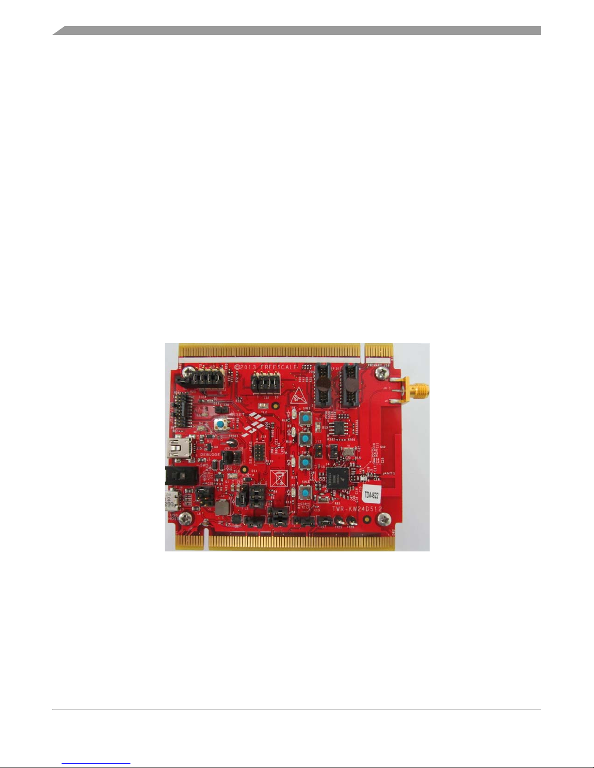
Figure 2-1 shows the TWR-KW2xDxxx development platform:
Figure 2-1. TWR-KW2XDXXX Development Platform
The TWR-KW2xDxxx development platform includes the following Features:
• Freescale’s low-power MKW21D256 or MKW24D512 SIP ZigBee™ platform device
• Fully compliant IEEE 802.15.4 Standard 2006 transceiver supports 250 kbps O-QPSK data in 5.0
MHz channels and full spread-spectrum encode and decode.
• Full IEEE 802.15.4 compliant wireless node; ZigBee capable with Freescale’ s BeeS tack software
stack.
T ower KW2xDxxx Hardware Reference Manual, Rev. 0.2
2-2 Freescale Semiconductor
Page 11

TWR-KW2xDxxx Development Platform Overview and Description
• Reference design area with small footprint, low cost RF node
— Differential input/output port used with external balun for single port operation
— Low external component count
— Programmable output power from –30 dBm to +8 dBm at the SMA connector.
— Receiver sensitivity: –100 dBm, typical (@1% PER for 20 byte payload packet) at the SMA
connector
• Integrated PCB inverted F-type antenna and SMA RF port
• Selectable power sources
• 32 MHz reference oscillator
• 32 kHz reference oscillator
• Pre-certified 2.4 GHz frequency band of operation (ISM)
• Programmable frequency clock output (CLK_OUT)
• External Serial flash for Over-the-air Programming (OTP) support
• General purpose TWRPI connector
•Interfaces:
— SPI, UART, and I2C interface configurations
— ADC and GPIO configurations
• Integrated open-standard serial and debug interface (OpenSDA)
• Supports full speed USB 2.0 (TWR-KW24D512 only)
• Cortex 20-pin (0.05”) JTAG debug port for target MCU
• Cortex 10-pin (0.05”) JTAG port for OpenSDA updates
• 4 blue LED indicators
• 4 push button switches
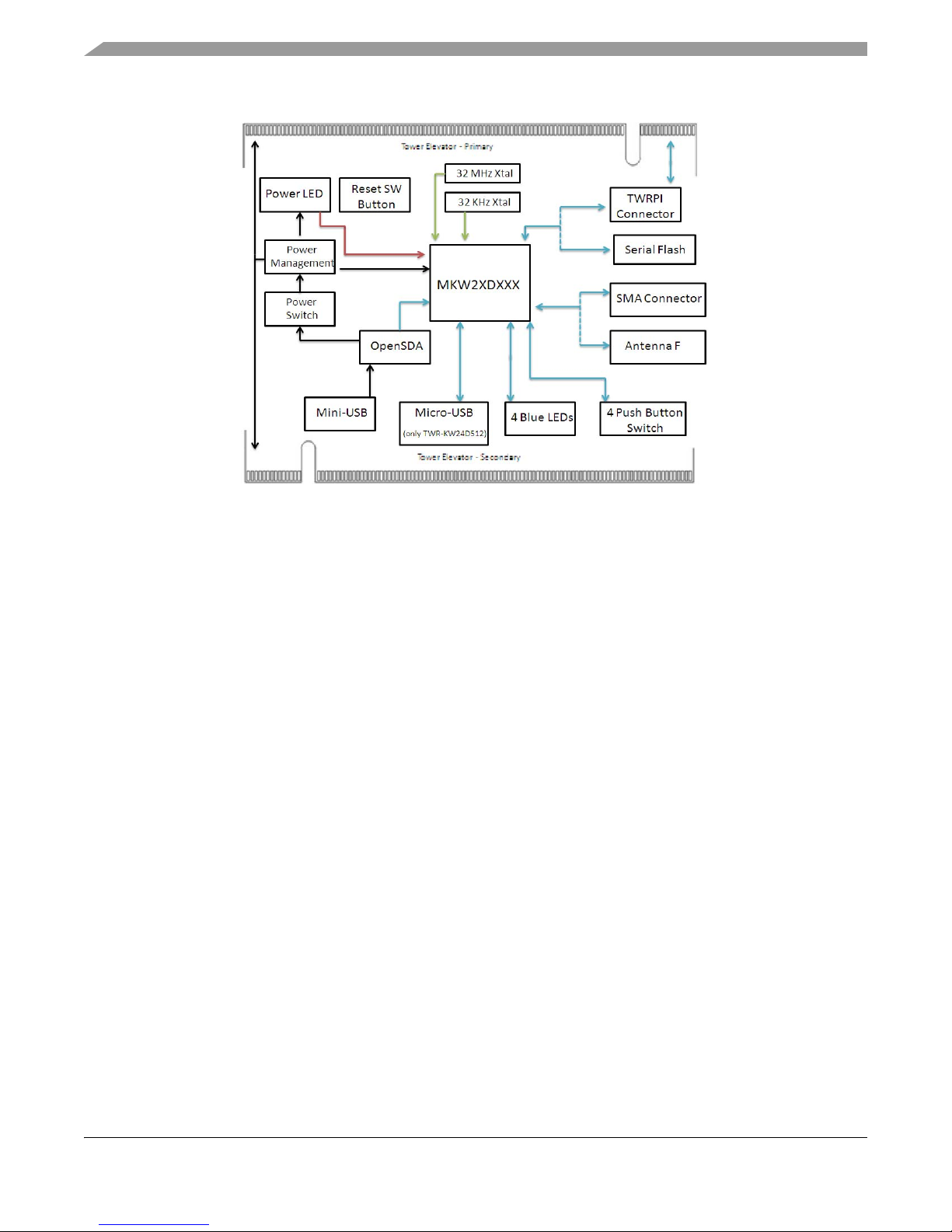
Figure 2-2 shows a simplified block diagram of the Freescale TWR-KW2XDXXX system.
T ower KW2xDxxx Hardware Reference Manual, Rev. 0.2
Freescale Semiconductor 2-3
Page 12
TWR-KW2xDxxx Development Platform Overview and Description
Figure 2-2. Simplified TWR-KW2xDxxx Block Diagram
2.3 Software and Driver Considerations
It is a good idea to install the BeeKit Wireless Connectivity Toolkit package found under Software and
Tools at the following URL before proceeding to use the TWR boards:
• www.freescale.com\zigbee
When users first connect a TWR-KW2xDxxx based platform to a PC, they may be prompted to install
drivers. If BeeKit is installed and this occurs, do not allow Windows to automatically search for and install
the drivers. Instead, select manual installation and steer Windows to the following directory:
C:\Program Files\Freescale\Drivers
Follow the instructions as they appear on the screen to complete driver installation.
NOTE
If installing the BeeKit software package to another drive or directory,
indicate the Drivers directory created by the installer in the custom location
where BeeKit was installed.
If BeeKit is not installed, note the following:
• The boards use the OpenSDA to USB converter, Virtual COM Port (VCP) driver for Windows.
• Download the appropriate driver and follow the instructions to complete driver installation.
— www.pemicro.com/opensda and download the Windows USB Drivers
T ower KW2xDxxx Hardware Reference Manual, Rev. 0.2
2-4 Freescale Semiconductor
Page 13

Chapter 3
TWR-KW2xDxxx
3.1 TWR-KW2xDxxx Overview
The TWR-KW2xDxxx is an evaluation board based on the Freescale MKW2xDxxx device. The
TWR-KW2xDxxx provides a platform to evaluate the TWR-KW2xDxxx SIP IC, develop software and
applications. The core device is accompanied by the 32 MHz reference oscillator crystal, RF circuitry
including PCB F-type antenna (or SMA), and supporting circuitry.
This basic board is intended as the core PCB for TWR-KW2xDxxx evaluation and application
development and can be used in the following modes:
• Simple standalone evaluation platform
• Daughtercard to other Development Platform boards (Tower System)
• Mothercard to an application specific dauhtercard, could be a TWRPI card.
3.1.1 PCB Board Features
The TWR-KW2xDxxx provides the following features:
• Freescale’s Tower System form factor
• 4-Layer metal, 0.062 inch thick FR4 board
• LGA footprint and power supply bypass
• Printed metal F-Antenna (and SMA)
• 32 MHz reference oscillator crystal
• 32.768 kHz crystal provided for optional timing oscillator.
• Standard Tower TWRPI daughter card mounting interface
— 20-Pin primary connector
— 20-Pin secondary connector
— Can provide main supply voltage to board
3.1.2 Form Factor
Figure 3-1 shows the TWR-KW2xDxxx connector and header locations.
T ower KW2xDxxx Hardware Reference Manual, Rev. 0.2
Freescale Semiconductor 3-1
Page 14

TWR-KW2xDxxx
Figure 3-1. TWR-KW2xDxxx Connector and Header Details
The TWR-KW2xDxxx incorporates the following general headers.
Headers J9 and J10:
• Both headers have standard 0.05in / 1.27 mm pin spacing
• J9 and J10 are 20-pin
• Both are pin headers mounted on the T op side of the board and are intended to plug into matching
receptacles on the TWRPI standard.
Headers J17 and J18:
• Both headers have standard 0.10in / 2.54 mm pin spacing
• J17 and J18 are 3x4-pin
• Both are pin headers mounted on the Top side of the board and are intended to have the capability
for SPI/TWR_Elevator Selector (J17) and UART1/TWR_Elevator Selector (J18).
Headers J19, J20, J21, and J24:
• Headers have standard 0.10in / 2.54 mm pin spacing
• J19, J20, J21, and J24 are 3-pin
• 19, J20, J21, and J24 are pin headers mounted on the Top side of the board and are intended to
select between UART0/LED.
T ower KW2xDxxx Hardware Reference Manual, Rev. 0.2
3-2 Freescale Semiconductor
Page 15

Figure 3-2 shows a footprint of the TWR-KW2xDxxx with the location of the IO Headers.
TWR-KW2xDxxx
Figure 3-2. TWR-KW2xDxxx T op Side (Component Side) Footprint
3.1.3 Board Level Specifications
Table 3-1. TWR-KW2xDxxx Specifications
Parameter Units Notes/Conditions
MIN TYP MAX
General
Size (PCB: X, Y) 90 x 80.6
3.54 x 3.175mminches
Layer build (PCB) 1.57
0.062
Dielectric material (PCB) FR4
Power
Current consumption
Transmit
Receive
18
20
18
20
mm
inches
mA
4-Layer
*Board level measured at J2.
Radio TX (Nominal power)
MCU
Radio RX mode
MCU
T ower KW2xDxxx Hardware Reference Manual, Rev. 0.2
Freescale Semiconductor 3-3
Page 16

TWR-KW2xDxxx
Table 3-1. TWR-KW2xDxxx Specifications (continued)
Parameter Units Notes/Conditions
Temperature
Operating temperature (see note) -40 +25 +70 °C • Operating temperature is limited to +70
°C due to switches. Basic circuit is good
for a maximum temperature of +85 °C.
Storage temperature -30 +25 +70 °C
RF
All 16 channels in the2450 MHz band
802.15.4 Frequency range 2405 2480 MHz
RF Receiver
Saturation (maximum input level) +10 dBm
Sensitivity for 1% packet error rate (PER)
-100 dBm
(+25 °C)
RF Transmitter
RF Power Output -32 +10 dBm Programmable in 2dB steps
2nd harmonic <-50 <-40 dBm Measured with output power set to nominal
(0 dBm) and temperature @ 25°C. Trap filter
is needed.
3rd harmonic <-50 <-40 dBm Measured with output power set to nominal
(0 dBm) and temperature @ 25°C. Trap filter
is needed.
Regulatory Approval
FCC Product is approved accordingly to the FCC
part 15 standard
CE (ETSI) Product is approved accordingly to the EN
300 328 V1.7.1 (2006-10) standard
CE (EMC) Product is approved accordingly to the EN
301 489-1 V1.6.1 (2005-09) and EN 301
489-17 V1.2.1 (2002-08) standards
Safety
UL Product is approved accordingly to the IEC
Environment
RoHS Product complies with the EU Directive
WEEE Product complies with the EU Directive
T ower KW2xDxxx Hardware Reference Manual, Rev. 0.2
3-4 Freescale Semiconductor
60950-1 and EN 60950-1, First Edition
standards
2002/95/EC of 27 January 2003
2002/95/EC of 27 January 2003
Page 17

TWR-KW2xDxxx
3.2 Functional Description
The TWR-KW2xDxxx is built around Freescale’ s MKW2XDXXX 56-pin LGA platform and is intended
as a simple evaluation platform and as a building block for application development. The 4-layer board
provides the MKW2XDXXX with its required RF circuitry , 32 MHz reference oscillator crystal and power
supply bypassing. The layout for this base level functionality can be used as a reference layout by the user
target board.
3.2.1 RF Performance and Considerations
TWR-KW2xDxxx transceiver includes a 1mW nominal output power, PA with internal voltage controlled
oscillator (VCO), integrated transmit/receive switch, on-board power supply regulation, and full
spread-spectrum encoding and decoding. Key specifications for MKW2XDXXX are:
• Nominal output power is 0 dBm, with +10 dBm max
• Programmable output power from –30 dBm to +10 dBm (measured at the package pin)
• Frequency range is 2360 to 2480 MHz (Includes both ISM and MBAN bands)
• Receiver sensitivity: –102 dBm, typical (@1% PER for 20 byte payload packet, measured at the
package pin)
• Differential bidirectional RF input/output port with integrated transmit/receive switch
The TWR-KW2xDxxx utilizes a minimum number of components while providing good RF performance:
• Uses a minimum number of RF marching components and external 50:50 balun.
• “F” printed metal antenna for a small footprint, low cost design.
An external 50 (unbal): 50(bal) balun connects a single-ended 50-ohm port to the differential RF port of
the MKW2XDXXX radio. The layout has provision for out-of-band signal suppression (components L5
and C19) if required.
T ower KW2xDxxx Hardware Reference Manual, Rev. 0.2
Freescale Semiconductor 3-5
Figure 3-3. TWR-KW2xDxxx RF Circuitry
Page 18

TWR-KW2xDxxx
3.2.2 Clocks
The TWR-KW2xDxxx provides two clocks:
• 32 MHz Reference Oscillator - Figure 3-4 shows the external 32 MHz external crystal Y1. This
mounted crystal must meet the MKW2XDXXX specifications. The IEEE 802.15.4 Standard
requires that the frequency be accurate to less that +/-40 ppm.
— Capacitors C21 and C22 provide the bulk of the crystal load capacitance. Onboard trim
capacitors can be programmed to center the frequency. At 25°C, it is desired to have the
frequency accurate to +/-10 ppm or less to allow for temperature variation.
— To measure the 32 MHz oscillator frequency, signal CLK_OUT (PTA18) can optionally be
programmed to provide a buffered output clock signal
— The TWR-KW2xDxxx has provision for injecting an external 32 MHz clock source as an
alternative to use of the onboard crystal:
– The crystal Y1 should be removed
– C20 must be mounted
– The ex ternal 32 MHz source is connected to 2-pin header J5; the frequency accuracy of the
external source must meet the +/-40 ppm of the IEEE 802.15.4
Figure 3-4. 32 MHz Reference Oscillator Circuit
• Optional 32.768 kHz Crystal Oscillator - Provision is also made for a secondary 32.768 kHz crystal
Y2 as shown in Figure 3-5. This oscillator can be used for a low power accurate time base.
— The module comes provided with the 32.768 kHz crystal.
— Load capacitors C23 and C24 provide the entire crystal load capacitance; there is no onboard
trim capacitance.
T ower KW2xDxxx Hardware Reference Manual, Rev. 0.2
3-6 Freescale Semiconductor
Page 19

Figure 3-5. 32.768 kHz Optional Oscillator Circuit
3.2.3 Power Management
The TWR-KW2xDxxx power management circuit is shown in Figure 3-6.
TWR-KW2xDxxx
Figure 3-6. TWR-KW2xDxxx Power Management Circuit
The TWR-KW2xDxxx has the flexibility to be powered in several configurations:
• Board can be supplied through the mini USB type B connector (J15) which provides P5V_USB to
J1 1-2.
• Board can be supplied through the micro USB AB (J6) (TWR-KW24D512 only) providing
P5V_KW24_USB to J27 1-2 and VOUT33 to J3 2-3.
• Board can be supplied through the TWR System Elevator headers which provides either
3.3V_ELEV or 5V_ELEV to header J1 3-4 or J1 5-6 respectively.
• Board can be supplied from an external DC supply in the following ways:
— Connect an USB battery adaptor capable of suppling 1.8 to 5.5 VDC to the micro USB AB (J6)
(TWR-KW24D512 only)
T ower KW2xDxxx Hardware Reference Manual, Rev. 0.2
Freescale Semiconductor 3-7
Page 20

TWR-KW2xDxxx
— An external unregulated supply up to 5.5VDC can be supplied to V_EXT header J28 making
use of the onboard 3.3 V LDO regulator
Header J2 provides the means to supply either the MCU, the radio and LED circuits. Current
measurements can be made by inserting a current meter in place of a designated jumper. Connections
configurations are described in Table 3-2.
Table 3-2. Power Distribution Header J2
Supply
Designation
V_LED 1 - 2 Supply voltage to power indicator LED
V_MCU 3 - 4 Supply voltage to MKW2xDxxx
V_RF 5 - 6 Supply voltage to MKW2xDxxx
Header
Pins
Description
• Normally jumpered
• Jumper used to enable LEDs on board
• Leave open for lowest power
• Usage: Measure LED current
• Normally jumpered
• Supplies only the MKW2xDxxx MCU
• Usage: Measure or supply MCU current
• Normally jumpered
• Supplies only the MKW2xDxxx transceiver
• Usage: Measure or supply radio current
3.2.4 TWR-KW2xDxxx Peripheral Functions
The TWR-KW2xDxxx includes the TWRPI general purpose peripheral function to assist in implementing
targeted applications. The TWR-KW2xDxxx board also has alternate port functions routed to the elevator
interface where off board tower system peripherals can be used if desired.
3.2.4.1 Serial FLASH (SPI Interface)
Component U13 is an AT45DB161E-SSHD 16 Mbit (2 Mbyte) serial Flash memory with SPI interface.
The memory is useful for over-the-air programming (OTAP) and for storage of non-volatile system data
or parameters. Figure 3-7 shows the memory circuit.
• Memory power supply is V_MCU
• Discrete pullup resistors for the SPI port are provided
• The SPI can be shared with another peripheral with the TWRPI J10 connector — an additional IO
signal would be required as a chip enable (CS or SS) for the peripheral. The normal SPI_SS and
the second chip select should NOT be active at the same time.
• The SPI Write Protect and Reset signals have discrete pullup resistors for control if required. The
resistors are DNP.
T ower KW2xDxxx Hardware Reference Manual, Rev. 0.2
3-8 Freescale Semiconductor
Page 21

TWR-KW2xDxxx
Figure 3-7. AT45DB161E-SSHD 16Mbit Serial FLASH memory
3.2.4.2 TWRPI Connectors J9 and J10
The two connectors J9 and J10 are 50 mil pin headers mounted on the front (component side) supporting
the standard TWRPI general purpose connector. The primary header J9 and secondary header J10 are
20-pin and mounted physically in such a manner as to prevent reverse insertion of any TWRPI card into
the motherboard receptacle (see Figure 3-1., “TWR-KW2xDxxx Connector and Header Details”).
• V_MCU provides the TWRPI connector its supply voltage
— Depending on power supply configuration, this voltage may supply the TWRPI card from the
TWR-KW2xDxxx. See Section 3.2.3, “Power Management”.
— Peripherals IO to the TWR-KW2xDxxx and the TWRPI card supply should use this same
voltage avoiding potential damage.
The pin definitions for the primary header J9 and the secondary header J10 are shown in Table 3-3.,
“TWRPI 20 Pin Primary Connector” and Table 3-4., “TWRPI 20 Pin Secondary Connector” respectively.
Table 3-3. TWRPI 20 Pin Primary Connector
Header
Pin
Number
1 5V_ELEV 5V VDD supply to board
2 V_MCU 3V3 VDD supply to board
3 GND Module ground
4 V_MCU 3V3 VDD supply to board
5 GND VSS (GND) board ground
6 GND VSS (GND) board ground
7 GND VSS (GND) board ground
8 PTE0_TWRPI ADC: Analog 0
TWR-MKW24D512 Pin Name Description
9 PTD1 ADC: Analog 1
10 GND VSS (GND) board ground
11 GND VSS (GND) board ground
T ower KW2xDxxx Hardware Reference Manual, Rev. 0.2
Freescale Semiconductor 3-9
Page 22

TWR-KW2xDxxx
Table 3-3. TWRPI 20 Pin Primary Connector
Header
Pin
TWR-MKW24D512 Pin Name Description
Number
12 PTE1_TWRPI ADC: Analog 2
13 GND VSS (GND) board ground
14 GND VSS (GND) board ground
15 GND GND board ground
16 GND GND board ground
17 PTE2_TWRPI ADC: TWRPI ID 0
18 PTE3_TWRPI ADC: TWRPI ID 1
19 GND GND board ground
20 RESET_B RESET
Table 3-4. TWRPI 20 Pin Secondary Connector
Header Pin
Number
TWR-KW24D512 Pin Name Description
1 GND Board ground
2 GND Board ground
3PTD2I2C: SCL
4PTD3I2C: SDA
5 GND Board ground
6 GND Board ground
7 GND Board ground
8 GND Board ground
9 PTB17_TWRPI SPI:MISO Master Input Slave Output
10 PTB16_TWRPI SPI:MOSI Master Output Slave Input
11 PTB10_TWRPI SPI: SS Slave Select
12 PTB11_TWRPI SPI:CLK R_SClock
13 GND Board ground
14 GND Board ground
15 GPIO1 GPIO: GPIO0/IRQ
16 GPIO2 GPIO; GPIO1/IRQ
17 PTE17/UART2_RX UART_RX or GPIO2
18 PTE16/UART2_TX UART_TX or GPIO3
T ower KW2xDxxx Hardware Reference Manual, Rev. 0.2
3-10 Freescale Semiconductor
Page 23

Table 3-4. TWRPI 20 Pin Secondary Connector
TWR-KW2xDxxx
Header Pin
Number
19 PTE18/UART2_CTS U ART_CTS or GPIO4/TIMER
20 PTE19/UAR T2_RTS UART_RTS or GPIO5/TIMER
TWR-KW24D512 Pin Name Description
3.2.4.3 Jumper Connectors
The TWR-KW2xDxxx development platform incorporates several headers which allow different MCU
port configurations assisting in the implementation of target applications. (see Figure 3-1.,
“TWR-KW2xDxxx Connector and Header Details”).
• SPI0 TWRPI / TWR_ELEV Select (J17).
— The TWR-KW2xDxxx has the capability to support a SPI for TWRPI boards - to configure,
shunt J17 pin 2-3 (SPI0_PCS), pin 5-6 (SPI0_SCK), 8-9 (SPI0_MOSI), and pin 11-12
(SPI0_MISO). See Figure 3-8., “TWR-KW24D512 Schematic”.
— The TWR-KW2xDxxx has the capability to support a TWR_ELEV with another TWR System
- to configure, shunt J17 pin 1-2 (SPI0_PCS), pin 4-5 (SPI0_SCK), 7-8 (SPI0_MOSI), and pin
10-11 (SPI0_MISO). See Figure 3-8., “TWR-KW24D512 Schematic”.
• UART1 / ADC TWRPI Select (J18).
— The TWR-KW2xDxxx has the capability to support a ADC for TWRPI boards - to configure,
shunt J18 pin 2-3 (ADC0_DM1), pin 5-6 (ADC0_DP1), 8-9 (ADC0_SE11), and pin 11-12
(ADC_SE10). See Figure 3-8., “TWR-KW24D512 Schematic”.
— The TWR-KW2xDxxx has the capability to support an UART1 connection trough
TWR_ELEV with another TWR System - to configure, shunt J17 pin 1-2 (UART1_TX), pin
4-5 (UART1_RX), 7-8 (UART1_CTS), and pin 10-11 (UART1_RTS). See Figure 3-8.
• UART0 / LED Select (J19/ J20/ J21/ J24).
— The TWR-KW2xDxxx has the capability to support the Blue LEDs on board - to configure,
shunt J19 pin 2-3 (P TD4_LED), J20 pin 2-3 (PTD5_LED), J21 pin 2-3 (PTD6_LED), and J24
pin 2-3 (PTD7_LED). See Figure 3-8., “TWR-KW24D512 Schematic”.
— The TWR-KW2xDxxx has the capability to support an UART0 connection trough
TWR_ELEV with another TWR System - to configure, shunt J19 pin 1-2 (UAR T0_RTS), J20
pin 1-2 (UART0_CTS), J21 pin 1-2 (UART0_Rx), and J24 pin 1-2 (UART0_TX). See
Figure 3-8., “TWR-KW24D512 Schematic”.
3.2.4.4 MKW24D512 USB Supply (J6) - TWR-MK24D512 Board Only
The MKW2xDxxx device has an on-board USB port which is configured to provide both power and serial
communication with the target MCU. (see Figure 3-1., “TWR-KW2xDxxx Connector and Header
Details”). The following jumpers allow the USB functionality:
• USB Select - Micro USB AB (J6).
T ower KW2xDxxx Hardware Reference Manual, Rev. 0.2
Freescale Semiconductor 3-11
Page 24

TWR-KW2xDxxx
— Shunt J27 to supply 5VDC to the MKW2xDxxx device (U3 pin 24, VREGIN) through the
Micro USB AB connector, This supplies the on-board USB regulator with then provides 3.3
VDC supply (U3 pin 23, VOUT33). See Figure 3-8., “TWR-KW24D512 Schematic”.
— Shunt J3 2-3 to supply power to the MKW2xDxxx device. See Figure 3-8., “TWR-KW24D512
Schematic”.
3.2.4.5 MKW21D256 (Non-USB) UART2 Support - TWR-MK21D256 Board Only
The MKW21D256 device does not support the USB interface and instead makes use of UART2 port
functionality . In this case, resistors are placed configuring UART2 use for both the TWRPI connector and
TWR elevator interface. (see Figure 3-1., “TWR-KW2xDxxx Connector and Header Details”).
• UART2/Non USB Select
— J27 is open, shunt J3 1-2, supply voltage required though power management configuration.
See Figure 3-8., “TWR-KW24D512 Schematic”, and Section 3.2.3, “Power Management”.
— The following resistors are placed: R84, R85, R86 and R87, keep as DNP, C27 and C28. See
Figure 3-8., “TWR-KW24D512 Schematic”.
T ower KW2xDxxx Hardware Reference Manual, Rev. 0.2
3-12 Freescale Semiconductor
Page 25

TWR-KW2xDxxx
Tower KW2xDxxx Hardware Reference Manual, Rev. 0.2
Freescale Semiconductor 3-13
3.3 Schematic, Board Layout, and Bill of Material
Figure 3-8. TWR-KW24D512 Schematic
5
5
4
4
3
3
2
2
1
1
D D
C C
B B
A A
3.3V BUCK/BOOST REGULATOR
TO USE TPS63000,
REPLACE RESISTORS WITH
THE FOLLOWING VALUES:
R1 = 100 OHM, R2 = 1.24M
AND POPULATE R5.
OUTPUT VOLTAGE WILL BE 3.6V
POWER SELECTOR
POWER ON
LED VOLTAGE
MCU VOLTAGE
RF VOLTAGE
Power Switch
SCH-27845
SEE NOTE C
External Voltage
P5V_USB
V_MAIN
V_REG
VCC
V_LED
V_MCU
V_RF
V_LED
3V3_ELEV
5V_ELEV
VREG_IN
VREG_IN
V_EXT
V_EXT
V_MAIN
VOUT33
VOUT33
VOUT33_SW
Drawing Title:
Size Document Number Rev
Date: Sheet
of
Page Title:
ICAP Classification: FCP: FIUO: PUBI:
C
TWR- KW24D512
C
Thursday, August 22, 2013
POWER SUPPLY
48
X ______
Drawing Title:
Size Document Number Rev
Date: Sheet of
Page Title:
ICAP Classification: FCP: FIUO: PUBI:
C
TWR- KW24D512
C
Thursday, August 22, 2013
POWER SUPPLY
48
X ______
Drawing Title:
Size Document Number Rev
Date: Sheet of
Page Title:
ICAP Classification: FCP: FIUO: PUBI:
C
TWR- KW24D512
C
Thursday, August 22, 2013
POWER SUPPLY
48
X ______
TP12
Q1
SI2305
1
32
D2
MBR0520LT1G
A C
TP10
J3
HDR TH 1X3
1
2
3
J1
HDR 2X3
1 2
3 4
65
TP2TP1
TP507
J28
HDR 1X2
1
2
R7
4.7K
R4 0R9
10K
TL3TL1 TL2
R6 0
C1
10UF
SW5
DPDT SWITCH
2
1
3
6
4
5
J2
HDR 2X3
1 2
3 4
65
R8 0
C4
0.1UF
TP4
U1
TPS63001
EN
6
GND
9
L14L2
2
PS/SYNC
7
VOUT1VIN
5
VINA
8
FB
10
PGND
3
PPAD
11
L1 3.3uH
1 2
C2
10UF
TP6
TP5
D4
GREEN
AC
R1
0
C3
10UF
TP9
TP7
R2
0
TP3
D1
MBR0520LT1G
A C
TP11
R10
330
D3
MBR0520LT1G
A C
R5
200K
DNP
Page 26

Tower KW2xDxxx Hardware Reference Manual, Rev. 0.2
3-14 Freescale Semiconductor
TWR-KW2xDxxx
5
5
4
4
3
3
2
2
1
1
D D
C C
B B
A A
32MHz XTAL
32kHz XTAL
XTAL_32M
XTAL_32K
HARMONIC TRAP
SCH-27845
USB / Non-USB SELECTOR
MKW24 (USB)
USB HOST
SEE NOTE A
SEE NOTE B
VBAT
EXTAL_32
RST_TGTMCU_B
XTAL_32M
EXTAL_32M
XTAL_32
Z_RF_N
Z_RF_P
XTAL_32
XTAL_32M_R
XTAL_32MEXTAL_32M
EXTAL_32K
CLK_OUT
EXTAL_32
RF_ANTRF_50
VDD_PA
VDD_IF
VDD_RF VDD_RF VDD_IF VDD_PA
VDD_REGD
VDD_REGD
P5V_K24_USB
KW24_USB_DP
K24_USB_SHLD
KW24_USB_DN PTE17/UART2_RX/USB_DN
PTE16/UART2_TX/USB_DP
PTE18/UART2_CTS/VOUT33
PTE19/UART2_RTS/VREGINP5V_KW24_USB
CLK_OUT
V_MCU
V_MCU
V_MCU
V_RF
V_MCU
GND
VOUT33_SW
PTC4
PTC6
PTC7
PTC5
PTD1
PTD4
PTD5
PTD6
PTD7
PTE0
PTE1
PTE16/UART2_TX/USB_DP
PTA1
PTA3
PTA4
PTA2
PTA0
GPIO2
GPIO1
RST_TGTMCU_B
PTE16/UART2_TX/USB_DP
PTE17/UART2_RX
PTE18/UART2_CTS
PTE16/UART2_TX
PTE17/UART2_RX/USB_DN
PTE18/UART2_CTS/VOUT33
PTE19/UART2_RTS/VREGIN
PTE19/UART2_RTS
PTE17/UART2_RX/USB_DN
PTE18/UART2_CTS/VOUT33
PTE19/UART2_RTS/VREGIN
PTE2
PTE3
PTE4
PTD3
PTD2
PTA19
Drawing Title:
Size Document Number Rev
Date: Sheet
of
Page Title:
ICAP Classification: FCP: FIUO: PUBI:
C
TWR- KW24D512
C
Thursday, August 22, 2013
MICROCONTROLLER
58
___ ___
X
Drawing Title:
Size Document Number Rev
Date: Sheet of
Page Title:
ICAP Classification: FCP: FIUO: PUBI:
C
TWR- KW24D512
C
Thursday, August 22, 2013
MICROCONTROLLER
58
___ ___
X
Drawing Title:
Size Document Number Rev
Date: Sheet of
Page Title:
ICAP Classification: FCP: FIUO: PUBI:
C
TWR- KW24D512
C
Thursday, August 22, 2013
MICROCONTROLLER
58
___ ___
X
R86 0
DNP
U3
MKW24D512V
VDD_MCU
20
VDDA
25
VREFH
26
VREFL
27
VSSA
28
VBAT_MCU
32
VDD_MCU
38
VBAT2_RF
42
VDD_REGD
43
VDD_PA
52
VDD_IF
53
VDD_RF
54
GND_PA363GND_PA148GND_PA2
51
EXTAL_32M
1
TAMPER0/RTC_WAKEUP
29
XTAL32
30
EXTAL32
31
RESET
41
RX_SWITCH
46
TX_SWITCH
47
RF_OUTP
49
RF_OUTN
50
XTAL_32M
56
GPIO1
2
GPIO2
3
PTA0/JTAG_TCLK/SWD_CLK/EZP_CLK/UART0_CTS/UART0_COL/FTM0_CH5
33
PTA1/JTAG_TDI/EZP_DI/UART0_RX/FTM0_CH6
34
PTA2/JTAG_TDO/TRACE_SWO/EZP_DO/UART0_TX/FTM0_CH7
35
PTA3/JTAG_TMS/SWD_DIO/UART0_RTS/FTM0_CH0
36
PTA4/LLWU_P3/NMI/EZP_CS/FTM0_CH1
37
PTA18/EXTAL0/FTM0_FLT2/FTM_CLKIN0
39
PTA19/XTAL0/FTM1_FLT0/FTM_CLKIN1/LPTMR0_ALT1
40
PTC4/LLWU_P8/SPI0_PCS0/UART1_TX/FTM0_CH3/CMP1_OUT
4
PTC5/LLWU_P9/SPI0_SCK/LPTMR0_ALT2/I2S0_RXD0/CMP0_OUT
5
PTC6/LLWU_P10/CMP0_IN0/SPI0_SOUT/PDB0_EXTRG/I2S0_RX_BCLK/I2S0_MCLK
6
PTC7/CMP0_IN1/SPI0_SIN/USB_SOF_OUT/I2S0_RX_FS
7
PTD1/ADC0_SE5B/SPI0_SCK/UART2_CTS
8
PTD2/LLWU_P13/SPI0_SOUT/UART2_RX/I2C_SCL/GPIO4_BSM_DATA
9
PTD3/SPI0_SIN/UART2_TX/I2C_SDA/GPIO5_BSM_CLK
10
PTD4/LLWU_P14/MADC0_SE21/SPI0_PCS1/UART0_RTS/FTM0_CH4/EWM_IN/GPIO_BSM_FRAME
11
PTD5/ADC0_SE6B/SPI0_PCS2/UART0_CTS/UART0_COL/FTM0_CH5/EWM_OUT
12
PTD6/LLWU_P15/ADC0_SE7B/SPI0_PCS3/UART0_RX/FTM0_CH6/FTM0_FLT0
13
PTD7/MADC0_SE22/CMT_IRO/UART0_TX/FTM0_CH7/FTM0_FLT1
14
PTE0/MADC0_SE10/SPI1_PCS1/UART1_TX/MTRACE_CLKOUT/I2C1_SDA/RTC_CLKOUT
15
PTE1/LLWU_P0/MADC0_SE11/SPI1_SOUT/UART1_RX/MTRACE_D3/I2C1_SCL/SPI1_SIN
16
USB0_DP
21
USB0_DM
22
VOUT33
23
VREGIN
24
PTE2/LLWU_P1/MADC0_DP1/SPI1_SCK/UART1_CTS/MTRACE_D2
17
PTE3/MADC0_DM1/SPI1_SIN/UART1_RTS/MTRACE_D1/SPI1_SOUT
18
PTE4/LLWU_P2/SPI1_PCS0/MTRACE_D0
19
EP_GND164EP_GND2
65
NC_57
57
NC_58
58
NC_59
59
NC_60
60
NC_61
61
NC_62
62
VBAT_RF
55
ANT_A
44
ANT_B
45
C44
5pF
R85 0
DNP
U10
12
J5
HDR 1X2
1
2
5VD-D+IDG
MICRO USB AB 5
J6
1
2
3
4
S2
5
S1
S3S4
C43
1000pF
R87 0
DNP
U11
12
C27
2.2UF
TP26
C14
0.1UF
C19
1.8pF
U12
12
TP25
R780
R13 0
Z1
2400MHz 50OHM
5
1
6
2
3
4
C46
1000pF
TP27
L4
330 OHM
1 2
L5
2.2nH
12
TP21
R82 0
C50
1.0UF
C28
0.1UF
R12
1.0M
TP22
C45
10PF
C13
0.1UF
R790
Y1
32MHZ
1 4
32
C8
5pF
R83 0
DNP
R14 0
J27
HDR 1X2 TH
1
2
Y2
32.768KHZ
21
C48
47PF
DNP
C7
0.33UF
L2 0
C21
12PF
R33 33
D15
MSS1P3L
A C
C9
1000pF
C36
0.1UF
DNP
C35
47PF
DNP
1
J4
SMA
R800
C17
10PF
R34 33
C42
0.1UF
D14
MSS1P3L
AC
L8
330 OHM
12
C10
5pF
ANT1
F_Antenna
C16
0.33UF
C23
12PF
C47
5pF
C11
1000pF
C20
10PF
DNP
C22
12PF
C25
1PF
C18
10PF
DNP
R15 0
C24
12PF
C15
33PF
R810
R840DNP
C12
0.1UF
L3 0
Page 27

TWR-KW2xDxxx
Tower KW2xDxxx Hardware Reference Manual, Rev. 0.2
Freescale Semiconductor 3-15
5
5
4
4
3
3
2
2
1
1
D D
C C
B B
A A
SWITCHING GPIO
LEDS
PIN FUNCTIONS USEDNET NAMES
PIN FUNCTIONS USEDNET NAMES
Default: 1-2
(Remove to measure
TWRPI current)
GENERAL PURPOSE
TWRPI
SPI0 TWRPI/TWR_ELEV Select
UART0/LED Select
UART1/ADC TWRPI/TWR_ELEV_Select
SCH-27845
NET NAMES PIN FUNCTIONS USED
NET NAMES PIN FUNCTIONS USED
SPI FLASH
SPI FLASHSPI FLASH
SPI FLASH
ADC0_DP0
SPI0_SIN_(MISO)PTB17 SPI0_SOUT_(MOSI)
RST_TGTMCU_B
TWRPI_ID1 ADC0_DM0
ADC1_DP0/ADC0_DP3
GPT_VDA
SPI0_SCK
GPT_VBRD
SPI0_PCS0PTB10
SPI0_PCS0_TWRPI
SPI0_SIN_(MISO)_TWRPI
SPI0_SCK_TWRPI
SPI0_SOUT_(MOSI)_TWRPI
ADC0_SE10
ADC0_DM1
ADC0_SE11
UART1_CTS
UART1_RTS
ADC0_DP1
UART1_TX
UART1_RX
UART0_CTSUART0_RTS
UART1_TX/MADC0_SE10
UART1_RX/MADC0_SE11
UART1_CTS/ADC0_DP1
UART1_RTS/ADC0_DM1
UART0_RX UART0_TX
SPI0_SCK
SPI0_PCS0
SPI0_SOUT
SPI0_SIN
V_LED
V_MCUV_MCU
V_MCU V_MCUV_MCU
5V_ELEV
V_MCU
V_MCU
V_MCU
PTD4_LED
PTD5_LED
PTD6_LED
PTD7_LED
PTC4
PTC5
PTC6
PTC7
PTE2_TWRPI
PTE3_TWRPI
RST_TGTMCU_B
PTE1_TWRPI
PTD3
PTB16_TWRPI
PTB11_TWRPI
GPIO2
PTE19/UART2_RTS
PTD2
PTB17_TWRPI
PTB10_TWRPI
GPIO1
PTE18/UART2_CTS
PTD1
PTE0_TWRPI
PTE17/UART2_RX
PTE16/UART2_TX
PTB10_TWRPI
PTB17_TWRPI
PTB11_TWRPI
PTC5
PTC4_A
PTC5_A
PTC7
PTC6
PTC4
PTC6_A
PTC7_A
PTB16_TWRPI
PTE0_TWRPI
PTE3_TWRPI
PTE1_TWRPI
PTE3
PTE2
PTE2_TWR
PTE3_TWR
PTE2_TWRPI PTD4_LED PTD5_LED
PTD4_TWR PTD5_TWR
PTE0_TWR
PTE1_TWR
PTD5PTD4
PTE0
PTE1
PTD6_LED
PTD6_TWR
PTD6
PTD7_LED
PTD7_TWR
PTD7
PTB17_TWRPI
PTB16_TWRPI
PTB11_TWRPI
PTB10_TWRPI
PTA19
PTE4
Drawing Title:
Size Document Number Rev
Date: Sheet
of
Page Title:
ICAP Classification: FCP: FIUO: PUBI:
C
TWR- KW24D512
C
Thursday, August 22, 2013
PERIPHERALS
68
___ ___
X
Drawing Title:
Size Document Number Rev
Date: Sheet
of
Page Title:
ICAP Classification: FCP: FIUO: PUBI:
C
TWR- KW24D512
C
Thursday, August 22, 2013
PERIPHERALS
68
___ ___
X
Drawing Title:
Size Document Number Rev
Date: Sheet
of
Page Title:
ICAP Classification: FCP: FIUO: PUBI:
C
TWR- KW24D512
C
Thursday, August 22, 2013
PERIPHERALS
68
___ ___
X
R21
4.7K
D5
BLUE
AC
TP502
R22
4.7K
J8
HDR 1X2 TH
1
2
D6
BLUE
AC
R553
10.0K
DNP
D7
BLUE
AC
R566
0
DNP
R563
10.0K
D8
BLUE
AC
R554
10.0K
DNP
R19
390
R20
0
R23
10.0K
R565
10.0K
J19
HDR TH 1X3
123
R555
10.0K
DNP
J9
CON_2X10
1 2
3 4
65
7 8
9 10
11 12
13 14
15 16
17 18
19 20
SW3 PB switch
1 4
2 3
J10
CON_2X10
1 2
3 4
65
7 8
9 10
11 12
13 14
15 16
17 18
19 20
R18
390
U13
AT45DB161E-SSHD
SCK
2
VCC
6
WP
5
RESET
3
GND
7
CS
4
SI
1
SO
8
R24
10.0K
J17
HDR 3X4
147
10
528
11
369
12
R16
390
SW4 PB switch
1 4
2 3
J20
HDR TH 1X3
123
R17
390
TP500
TP14
SW1 PB switch
1 4
2 3
TP15
J21
HDR TH 1X3
123
R564
0
DNP
J18
HDR 3X4
147
10
528
11
369
12
TP16
TP504
SW2 PB switch
1 4
2 3
TP17
TP506
TP501
J24
HDR TH 1X3
123
R552
10.0K
DNP
Page 28

Tower KW2xDxxx Hardware Reference Manual, Rev. 0.2
3-16 Freescale Semiconductor
TWR-KW2xDxxx
5
5
4
4
3
3
2
2
1
1
D D
C C
B B
A A
PIN FUNCTIONS USED NET NAMES
JTAG / SWD CONNECTOR
SCH-27845
TARGET MCU
INTERFACE
SIGNALS
PU/PD LOGIC:
SERIAL INTERFACE
IS ALWAYS RESET
WHEN USB PORT
IS DISCONNECTED
OpenSDA INTERFACE
OpenSDA INTERFACE JTAG CONNECTOR
SPARE 74HC125 buffer
KEY - PIN 7
Default: no shunt
(Disconnect Target Power)
DEBUGGER
TX
RX
CTS
RTS
MANUAL
RESET
RST_TGTMCU_B
JTAG_TCLK/SWD_CLK/EZP_CLK PTA0
JTAG_TMS/SWD_DIO PTA3
SDA_RST
TC_EXTAL_TP
TC_XTAL_TP
SDA_SWD_OE_B
UART1_RX_TGTMCU
UART1_TX_TGTMCU
SDA_EXTAL
SDA_XTAL
TC_SDA_USB_ID_TP
SWD_DIO_TGTMCU
SDA_USB_CONN_DP
SDA_USB_CONN_DN
SDA_SPI0_SOUT
SDA_USBSHIELD
P5V0_SDA_USB_CONN_VBUS
SDA_USB_VOUT33
SDA_JTAG_TCLK
SDA_JTAG_TDI
SDA_JTAG_TDO
SDA_JTAG_TMS
UART1_TX_TGTMCU
UART1_RX_TGTMCU
SDA_SPI0_SCK
SDA_LED
SDA_SPI0_SIN
SDA_LED_R
SDA_RST
SDA_JTAG_TCLK
SDA_JTAG_TDI
SDA_JTAG_TDO
SDA_JTAG_TMS
TC_74125_SPARE_O_TPTC_74125_SPARE_I_TP
PTA2JTAG_TDO/TRACE_SWO/EZP_DO
PTA1JTAG_TDI/EZP_DI
VTRG_FAULT_B
POWER_EN
VTRG_ENPOWER_EN
VTRG_FAULT_B
PTA4 EZP_CS_B EZP_CSR_B
TGT_PWR
UART1_CTS_TGTMCU
UART1_RST_TGTMCU
TRACE_CLKOUT
TRACE_D0
TRACE_D3
TRACE_D2
TRACE_D1
UART1_CTS_TGTMCU
UART1_RST_TGTMCU
SDA_SWD_EN
SWD_CLK_TGTMCU
RESET_B
RSTR
SDA_USB_DP
SDA_USB_DN
V_MCU
GND
GND
GND
GND
GND
GND
GND
GND
P5V_SDA
GND GND
GND
GND
SDA_USB_VOUT33
P5V_SDA
SDA_USB_VOUT33
SDA_USB_VOUT33
GNDGND
GND
SDA_USB_VOUT33
P5V_SDA
SDA_USB_VOUT33
GND
SDA_USB_VOUT33
SDA_USB_VOUT33
P5V_SDA
P5V_USB
SDA_USB_VOUT33
5V_ELEV
V_MCUV_MCU
P5V_USB
SDA_USB_VOUT33
V_LED
SDA_USB_VOUT33
V_MCU
SDA_USB_VOUT33
V_MCU
SDA_USB_VOUT33
RST_TGTMCU_B4,7,8
PTA0
PTA3
RESET_B
PTE0_TWR
PTE1_TWR
PTA3
PTA0
PTA2
PTA1
ELE_PS_SENSE8
PTA4
PTE2_TWR
PTE3_TWR
PTE0
PTE4
PTE3
PTE2
PTE1
RST_TGTMCU_B
Drawing Title:
Size Document Number Rev
Date: Sheet
of
Page Title:
ICAP Classification: FCP: FIUO: PUBI:
C
TWR- KW24D512
C
Thursday, August 22, 2013
OpenSDA
78
___ ___
X
Drawing Title:
Size Document Number Rev
Date: Sheet
of
Page Title:
ICAP Classification: FCP: FIUO: PUBI:
C
TWR- KW24D512
C
Thursday, August 22, 2013
OpenSDA
78
___ ___
X
Drawing Title:
Size Document Number Rev
Date: Sheet
of
Page Title:
ICAP Classification: FCP: FIUO: PUBI:
C
TWR- KW24D512
C
Thursday, August 22, 2013
OpenSDA
78
___ ___
X
D9
ORANGE
AC
TP101
U14
TXS0101
VCCA
1
GND
2
A3B
4
OE
5
VCCB
6
R560
10K
GND2
GND1
Y3
8MHZ
1 2
34
R110
10.0K
U4C
74LVC125ADB
98
10
R94 0
TP509
TP102
R90 1.0K
TP105
TP103
R26
10.0K
R46
330
D12 MSS1P3L
A C
C33
0.1UF
TP510
R104
220
R91 1.0K
R108
10.0K
DNP
L7
330 OHM
1 2
R112
27K
DNP
TP511
R88 1.0K
R25
10.0K
R562
100K
J30
HDR 1X2
1
2
R106
27K
R109
15K
R27 0
DNP
C49
1.0UF
R92 1.0K
R111 1K
J12
HDR 1X2 TH
1
2
TP512
R551 1.0K
U8
GSOT05C-GS08
1
2
3
C30
22PF
DNP
Q2
MMBT2484L
2 3
1
U4B
74LVC125ADB
5 6
4
D13
MSS1P3L
A C
PK20DX128VFM5
U6
VDD1
1
VSS1
2
VDDA
7
VSSA
8
VBAT
11
JTAG_TCLK/SWD_CLK/EZP_CLK/TSI0_CH1/PTA0/UART0_CTS/UART0_COL/FTM0_CH5
12
JTAG_TDI/EZP_DI/TSI0_CH2/PTA1/UART0_RX/FTM0_CH6
13
JTAG_TDO/TRACE_SWO/EZP_DO/TSI0_CH3/PTA2/UART0_TX/FTM0_CH7
14
JTAG_TMS/SWD_DIO/TSI0_CH4/PTA3/UART0_RTS/FTM0_CH0
15
NMI/EZP_CS/TSI0_CH5/PTA4/FTM0_CH1/LLWU_P3
16
EXTAL0/PTA18/FTM0_FLT2/FTM_CLKIN0
17
XTAL0/PTA19/FTM1_FLT0/FTM_CLKIN1/LPTMR0_ALT1
18
ADC0_SE8/TSI0_CH0/PTB0/I2C0_SCL/FTM1_CH0/FTM1_QD_PHA/LLWU_P5
20
ADC0_SE9/TSI0_CH6/PTB1/I2C0_SDA/FTM1_CH1/FTM1_QD_PHB
21
ADC0_SE4B/CMP1_IN0/TSI0_CH15/PTC2/SPI0_PCS2/UART1_CTS/FTM0_CH1/I2S0_TX_FS
23
CMP1_IN1/PTC3/SPI0_PCS1/UART1_RX/FTM0_CH2/I2S0_TX_BCLK/LLWU_P7
24
PTC4/SPI0_PCS0/UART1_TX/FTM0_CH3/CMP1_OUT/LLWU_P8
25
PTC5/SPI0_SCK/LPTMR0_ALT2/I2S0_RXD0/CMP0_OUT/LLWU_P9
26
CMP0_IN0/PTC6/SPI0_SOUT/PDB0_EXTRG/I2S0_RX_BCLK/I2S0_MCLK/LLWU_P10
27
CMP0_IN1/PTC7/SPI0_SIN/USB_SOF_OUT/I2S0_RX_FS
28
PTD4/SPI0_PCS1/UART0_RTS/FTM0_CH4/EWM_IN/LLWU_P14
29
ADC0_SE6B/PTD5/SPI0_PCS2/UART0_CTS/UART0_COL/FTM0_CH5/EWM_OUT
30
ADC0_SE7B/PTD6/SPI0_PCS3/UART0_RX/FTM0_CH6/FTM0_FLT0/LLWU_P15
31
PTD7/CMT_IRO/UART0_TX/FTM0_CH7/FTM0_FLT1
32
VREGIN
6
VOUT33
5
USB0_DM
4
USB0_DP
3
EXTAL32
10
XTAL32
9
RESET
19
ADC0_SE15/TSI0_CH14/PTC1/SPI0_PCS3/UART1_RTS/FTM0_CH0/I2S0_TXD0/LLWU_P6
22
EPAD
33
VCC
GND
U4A
74LVC125ADB
2 3
14
1
7
R95
0
TP108
J29
HDR 1X2
1
2
C34
18PF
DNP
U4D
74LVC125ADB
12 11
13
R51 33
TP100
TP107
R52
4.7K
U7
MIC2005-0.8YM6
VOUT
6
CSLEW
5
ENABLE3GND
2
VIN
1
FAULT
4
TP106
R100
10K
C26
1.0UF
C31
22PF
DNP
C29
0.1UF
TP508
R89 1.0K
R105
10K
R93 1.0K
J11
HDR_19P
1 2
3 4
65
8
9 10
11 12
13 14
15 16
17 18
19 20
C32
2.2UF
J13
HDR 2X5
1 2
3 4
65
7 8
9 10
D16
CDSQR400B
AC
SW6
PB switch
14
23
R50 33
L6
330 OHM
1 2
5VD-D+IDG
CONN USB MINI-B
J15
1
2
3
4
S2
5
S1
S3S4
R107
10K
TP104
D11LED GREEN
AC
Page 29

TWR-KW2xDxxx
Tower KW2xDxxx Hardware Reference Manual, Rev. 0.2
Freescale Semiconductor 3-17
5
5
4
4
3
3
2
2
1
1
D D
C C
B B
A A
SCH-27845
ADC0_SE8PTB0
ADC0_SE9PTE1
3V3_ELEV
5V_ELEV
3V3_ELEV
5V_ELEV
3V3_ELEV
5V_ELEV
5V_ELEV
3V3_ELEV
ELE_PS_SENSE
PTC4
PTC5
PTC6
PTC7
PTD1
PTC6_A
PTD2
PTD3
PTC7_A
PTD4
PTD4_TWR
PTD5_TWR
PTD6_TWR
PTD6_TWR
PTE0_TWR
PTE3_TWR
PTE2_TWR
PTD2
PTD3
PTD2
PTD3
PTD3
PTD2
PTB17_TWRPI
PTB17_TWRPI
PTB16_TWRPI
PTB16_TWRPI
PTB10_TWRPI
PTB10_TWRPI
PTB11_TWRPI
PTB11_TWRPI
PTE3_TWRPI
PTE1_TWRPI
PTE0
PTE1_TWR
PTE3_TWR
PTE2_TWR
PTC4_A
PTC5_A
PTE1_TWR
PTE0_TWR
PTD6_TWR
PTD7_TWR
PTE18/UART2_CTS
PTE19/UART2_RTS
PTE17/UART2_RX
GPIO1
GPIO2
PTD2
PTE16/UART2_TX
RST_TGTMCU_B
Drawing Title:
Size Document Number Rev
Date: Sheet
of
Page Title:
ICAP Classification: FCP: FIUO: PUBI:
C
TWR- KW24D512
C
Thursday, August 22, 2013
TOWER CONNECTORS
88
___ ___
X
Drawing Title:
Size Document Number Rev
Date: Sheet
of
Page Title:
ICAP Classification: FCP: FIUO: PUBI:
C
TWR- KW24D512
C
Thursday, August 22, 2013
TOWER CONNECTORS
88
___ ___
X
Drawing Title:
Size Document Number Rev
Date: Sheet
of
Page Title:
ICAP Classification: FCP: FIUO: PUBI:
C
TWR- KW24D512
C
Thursday, August 22, 2013
TOWER CONNECTORS
88
___ ___
X
R5610
DNP
R720 DNP
R740 DNP
R660 DNP
R770 DNP
SECONDARYPCI EXPRESS TOWER SYSTEM
J16B
5V_3
D1
GND_17
D2
3.3V_8
D3
ELE_PS_SENSE_2
D4
GND_18
D5
GND_19
D6
SPI2_CLK
D7
SPI2_CS1
D8
SPI2_CS0
D9
SPI2_MOSI
D10
SPI2_MISO
D11
ETH_COL_2
D12
ETH_RXER_2
D13
ETH_TXCLK_2
D14
ETH_TXEN_2
D15
GPIO18
D16
GPIO19/SDHC_D4
D17
GPIO20/SDHC_D5
D18
ETH_TXD1_2
D19
ETH_TXD0_2
D20
ULPI_NEXT/USB_HS_DM
D21
ULPI_DIR/USB_HS_DP
D22
UPLI_DATA5/USB_HS_VBUS
D23
ULPI_DATA6/USB_HS_ID
D24
ULPI_DATA7
D25
GND_20
D26
LCD_HSYNC/LCD_P24
D27
LCD_VSYNC/LCD_P25
D28
AN13
D29
AN12
D30
GND_21
D31
LCD_CLK/LCD_P26
D32
TMR11
D33
TMR10
D34
GPIO21
D35
3.3V_9
D36
PWM15
D37
PWM14
D38
PWM13
D39
PWM12
D40
CAN2_RX
D41
CAN2_TX
D42
LCD_CONTRAST
D43
LCD_OE/LCD_P27
D44
LCD_D0/LCD_P0
D45
LCD_D1/LCD_P1
D46
LCD_D2/LCD_P2
D47
LCD_D3/LCD_P3
D48
GND_22
D49
GPIO23
D50
GPIO24
D51
LCD_D12/LCD_P12
D52
LCD_D13/LCD_P13
D53
LCD_D14/LCD_P14
D54
IRQ_P/SPI2_CS2
D55
IRQ_O/SPI2_CS3
D56
IRQ_N
D57
IRQ_M
D58
IRQ_L
D59
IRQ_K
D60
IRQ_J
D61
IRQ_I
D62
LCD_D18/LCD_P18/SD_RX_0+
D63
LCD_D19/LCD_P19/SD_RX_0-
D64
GND_23
D65
EBI_AD20/LCD_P42/SD_GND
D66
EBI_AD21/LCD_P43/SD_GND
D67
EBI_AD22/LCD_P44/SD_RX_1+
D68
EBI_AD23/LCD_P45/SD_RX_1-
D69
EBI_AD24/LCD_P46/SD_GND
D70
EBI_AD25/LCD_P47/SD_GND
D71
EBI_AD26/LCD_P48/SD_RX_2+
D72
EBI_AD27/LCD_P49/SD_RX_2-
D73
EBI_AD28/LCD_P50/SD_GND
D74
EBI_AD29/LCD_P51/SD_GND
D75
EBI_AD30/LCD_P52/SD_RX_3+
D76
EBI_AD31/LCD_P53/SD_RX_3-
D77
LCD_D20/LCD_P20/SD_GND
D78
LCD_D21/LCD_P21/SD_REFCLK+
D79
LCD_D22/LCD_P22/SD_REFCLK-
D80
GND_24
D81
3.3V_10
D82
5V_4
C1
GND_25
C2
3.3V_11
C3
3.3V_12
C4
GND_26
C5
GND_27
C6
I2C2_SCL
C7
I2C2_SDA
C8
GPIO25
C9
ULPI_STOP
C10
ULPI_CLK
C11
GPIO26
C12
ETH_MDC_2
C13
ETH_MDIO_2
C14
ETH_RXCLK_2
C15
ETH_RXDV_2
C16
GPIO27/SDHC_D6
C17
GPIO28/SDHC_D7
C18
ETH_RXD1_2
C19
ETH_RXD0_2
C20
ULPI_DATA0/I2S1_MCLK
C21
ULPI_DATA1/I2S1_DOUT_SCK
C22
ULPI_DATA2/I2S1_DOUT_WS
C23
ULPI_DATA3/I2S1_DIN0
C24
ULPI_DATA4/I2S1_DOUT0
C25
GND_28
C26
AN11
C27
AN10
C28
AN9
C29
AN8
C30
GND_29
C31
GPIO29/UART2_DCD
C32
TMR9
C33
TMR8
C34
GPIO30/UART3_DCD
C35
3.3V_13
C36
PWM11
C37
PWM10
C38
PWM9
C39
PWM8
C40
UART2_RXD/TSI0
C41
UART2_TXD/TSI1
C42
UART2_RTS/TSI2
C43
UART2_CTS/TSI3
C44
UART3_RXD/TSI4
C45
UART3_TXD/TSI5
C46
UART3_RTS/CAN3_RX
C47
UART3_CTS/CAN3_TX
C48
GND_30
C49
LCD_D4/LCD_P4
C50
LCD_D5/LCD_P5
C51
LCD_D6/LCD_P6
C52
LCD_D7/LCD_P7
C53
LCD_D8/LCD_P8
C54
LCD_D9/LCD_P9
C55
LCD_D10/LCD_P10
C56
LCD_D11/LCD_P11
C57
I2S1_DIN_SCK
C58
I2S1_DIN_WS
C59
I2S1_DIN1
C60
I2S1_DOUT1
C61
LCD_D15/LCD_P15
C62
LCD_D16/LCD_P16/SD_GND
C63
LCD_D17/LCD_P17/SD_GND
C64
GND_31
C65
EBI_BE_32_24/LCD_P28/SD_TX_0+
C66
EBI_BE_23_16/LCD_P29/SD_TX_0-
C67
EBI_BE_15_8/LCD_P30/SD_GND
C68
EBI_BE_7_0/LCD_P31/SD_GND
C69
EBI_TSIZE0/LCD_P32/SD_TX_1+
C70
EBI_TSIZE1/LCD_P33/SD_TX_1-
C71
EBI_TS/LCD_P34/SD_GND
C72
EBI_TBST/LCD_P35/SD_GND
C73
EBI_TA/LCD_P36/SD_TX_2+
C74
EBI_CS4/LCD_P37/SD_TX_2-
C75
EBI_CS3/LCD_P38/SD_GND
C76
EBI_CS2/LCD_P39/SD_GND
C77
EBI_CS1/LCD_P40/SD_TX_3+
C78
GPIO31/LCD_P41/SD_TX_3-
C79
LCD_D23/LCD_P23/SD_GND
C80
GND_32
C81
3.3V_14
C82
PRIMARYPCI EXPRESS TOWER SYSTEM
J16A
5V_1
B1
GND_1
B2
3.3V_1
B3
ELE_PS_SENSE_1
B4
GND_2
B5
GND_3
B6
SDHC_CLK/SPI1_CLK
B7
SDHC_D3/SPI1_CS1
B8
SDHC_D3/SPI1_CS0
B9
SDHC_CMD/SPI1_MOSI
B10
SDHC_D0/SPI1_MISO
B11
ETH_COL_1
B12
ETH_RXER_1
B13
ETH_TXCLK_1
B14
ETH_TXEN_1
B15
ETH_TXER
B16
ETH_TXD3
B17
ETH_TXD2
B18
ETH_TXD1_1
B19
ETH_TXD0_1
B20
GPIO1/UART1_RTS
B21
GPIO2/SDHC_D1
B22
GPIO3
B23
CLKIN0
B24
CLKOUT1
B25
GND_4
B26
AN7
B27
AN6
B28
AN5
B29
AN4
B30
GND_5
B31
DAC1
B32
TMR3
B33
TMR2
B34
GPIO4
B35
3.3V_2
B36
PWM7
B37
PWM6
B38
PWM5
B39
PWM4
B40
CAN0_RX
B41
CAN0_TX
B42
1WIRE
B43
SPI0_MISO/IO1
B44
SPI0_MOSI/IO0
B45
SPI0_CS0
B46
SPI0_CS1
B47
SPI0_CLK
B48
GND_6
B49
I2C1_SCL
B50
I2C1_SDA
B51
GPIO5/SPI0_HOLD/IO3
B52
RSRV_B53
B53
RSRV_B54
B54
IRQ_H
B55
IRQ_G
B56
IRQ_F
B57
IRQ_E
B58
IRQ_D
B59
IRQ_C
B60
IRQ_B
B61
IRQ_A
B62
EBI_ALE/EBI_CS1
B63
EBI_CS0
B64
GND_7
B65
EBI_AD15
B66
EBI_AD16
B67
EBI_AD17
B68
EBI_AD18
B69
EBI_AD19
B70
EBI_R/W
B71
EBI_OE
B72
EBI_D7
B73
EBI_D6
B74
EBI_D5
B75
EBI_D4
B76
EBI_D3
B77
EBI_D2
B78
EBI_D1
B79
EBI_D0
B80
GND_8
B81
3.3V_3
B82
5V_2
A1
GND_9
A2
3.3V_4
A3
3.3V_5
A4
GND_10
A5
GND_11
A6
I2C0_SCL
A7
I2C0_SDA
A8
GPIO9/UART1_CTS
A9
GPIO8/SDHC_D2
A10
GPIO7/SD_WP_DET
A11
ETH_CRS
A12
ETH_MDC_1
A13
ETH_MDIO_1
A14
ETH_RXCLK_1
A15
ETH_RXDV_1
A16
ETH_RXD3
A17
ETH_RXD2
A18
ETH_RXD1_1
A19
ETH_RXD0_1
A20
I2S0_MCLK
A21
I2S0_DOUT_SCK
A22
I2S0_DOUT_WS
A23
I2S0_DIN0
A24
I2S0_DOUT0
A25
GND_12
A26
AN3
A27
AN2
A28
AN1
A29
AN0
A30
GND_13
A31
DAC0
A32
TMR1
A33
TMR0
A34
GPIO6
A35
3.3V_6
A36
PWM3
A37
PWM2
A38
PWM1
A39
PWM0
A40
UART0_RX
A41
UART0_TX
A42
UART1_RX
A43
UART1_TX
A44
VSSA
A45
VDDA
A46
CAN1_RX
A47
CAN1_TX
A48
GND_14
A49
GPIO14
A50
GPIO15
A51
GPIO16/SPI0_WP/IO2
A52
GPIO17
A53
USB0_DM
A54
USB0_DP
A55
USB0_ID
A56
USB0_VBUS
A57
I2S0_DIN_SCK
A58
I2S0_DIN_WS
A59
I2S0_DIN1
A60
I2S0_DOUT1
A61
RSTIN
A62
RSTOUT
A63
CLKOUT0
A64
GND_15
A65
EBI_AD14
A66
EBI_AD13
A67
EBI_AD12
A68
EBI_AD11
A69
EBI_AD10
A70
EBI_AD9
A71
EBI_AD8
A72
EBI_AD7
A73
EBI_AD6
A74
EBI_AD5
A75
EBI_AD4
A76
EBI_AD3
A77
EBI_AD2
A78
EBI_AD1
A79
EBI_AD0
A80
GND_16
A81
3.3V_7
A82
R650
DNP
R730 DNP
R600
R670DNP
R620DNP
R590DNP
R700 DNP
R750DNP
R630
R640
DNP
R680DNP
R580 DNP
R710 DNP
R610DNP
R760DNP
R690DNP
Page 30

TWR-KW2xDxxx
Figure 3-9. TWR-KW24D512 Reference Board PCB Component Location (Top View)
Figure 3-10. TWR-KW24D512 Reference Board PCB Test Points
T ower KW2xDxxx Hardware Reference Manual, Rev. 0.2
3-18 Freescale Semiconductor
Page 31

TWR-KW2xDxxx
Figure 3-11. TWR-KW24D512 Reference Board PCB Layout (Top View)
Figure 3-12. TWR-KW24D512 Reference Board PCB Layout (Bottom View)
T ower KW2xDxxx Hardware Reference Manual, Rev. 0.2
Freescale Semiconductor 3-19
Page 32

TWR-KW2xDxxx
3.3.1 Bill of Materials
Table 3-5. Bill of Materials (Common parts for all frequency bands) (Sheet 1 of 6)
Item Qty Reference Value Description Mfg. Name Mfg. Part Number
1 1 ANT1 F_Antenna PCB F ANTENNA, NO PART
ORDER
2 1 D16 CDSQR400BDIODE SW 0.1A 80V SOD-923F COMCHIP
TECHNOLOGY CO.
3 3 C1,C2,C3 10UF CAP CER 10UF 10V 10% X7R
0805
46C4,C12,C1
3,C14,C29,
C42
5 2 C7,C16 0.33UF CAP CER 0.33UF 6.3V 10% X5R
64C8,C10,C4
4,C47
7 5 R108,R552
,R553,R55
4,R555
DNP
84C9,C11,C4
3,C46
9 1 C15 33PF CAP CER 33PF 50V 5% C0G 0402 VENKEL COMPANY C0402C0G500-330JN
10 2 C18,C20,
DNP
0.1UF CAP CER 0.1UF 16V 10% X7R
0402
0402
5pF CAP CER 5PF 16V 5% C0G
CC0402
10.0K RES MF 10.0K 1/16W 1%
AEC-Q200 0402
1000pF CAP CER 1000PF 50V 5% C0G
0402
10PF CAP CER 10PF 50V 5% C0G
040210PF
Murata GRM21BR71A106KE
Kemet C0402C104K4RAC
Murata GRM155R60J334KE0
SMEC MCCA050J0NOTF
VISHAY
INTERTECHNOLOGY
MURATA GRM1555C1H102JA0
AVX 04025A100JAT2A
CDSQR400B
51L
1D
CRCW040210K0FKE
D
1D
E
11 2 C17,C45 10PF CAP CER 10PF 50V 5% C0G
040210PF
12 1 C19 1.8pF CAP CER 1.8PF 50V 0.25PF C0G
0402
13 4 C21,C22,C
23,C24
14 1 C25 1PF CAP CER 1PF 50V 5% C0G 0402 MURATA GRM1555C1H1R0CA
15 3 C26,C49,C501.0UF CAP CER 1.0UF 10V 10% X5R
16 2 C27,C32 2.2UF CAP CER 2.2UF 10V 10% X7R
17 2 C28,C33 0.1UF CAP CER 0.1UF 10V 10% X5R
18 2 C30,C31 22PF
3-20 Freescale Semiconductor
12PF CAP CER 12PF 50V 5% C0G 0402 MURA T A GRM1555C1H120JZ0
0402
0603
0402
CAP CER 22PF 50V 5% C0G 0402 AVX 04025A220JAT2A
DNP
T ower KW2xDxxx Hardware Reference Manual, Rev. 0.2
AVX 04025A100JAT2A
KEMET C0402C189C5GAC
1D
01B
YAGEO AMERICA CC0402KRX5R6BB10
5
MURATA GRM188R71A225KE1
5D
KEMET C0402C104K8PAC
Page 33

TWR-KW2xDxxx
Table 3-5. Bill of Materials (Common parts for all frequency bands) (Sheet 2 of 6)
Item Qty Reference Value Description Mfg. Name Mfg. Part Number
19 1 C34 18PF
DNP
20 2 C35,C48 47PF
CAP CER 18PF 50V 5% C0G 0603 YAGEO AMERICA CC0603JRNPO9BN18
0
CAP CER 47PF 16V 5% C0G 0402 AVX 0402YA470JA T2A
DNP
21 1 C36 0.1UF
DNP
22 3 D1,D2,D3 MBR0520LT1GDIODE SCH 0.5A 20V SOD-123 ON
CAP CER 0.1UF 16V 10% X7R
0402
KEMET C0402C104K4RAC
MBR0520LT1G
SEMICONDUCTOR
23 1 D4 GREEN LED GRN SGL 30MA SMT 0805 LITE ON LTST-C171KGKT
24 4 D5,D6,D7,D8BLUE LED BLUE SGL 20MA SMT 0805 LITE ON LTST-C171TBKT
25 1 D9 ORANGE LED ULTRA BRIGHT ORANGE
LITE ON LTST-C190KFKT
20MA 2V SMT 0603
26 1 D11 LED
LED GRN SGL 20MA 0603 OSRAM LG L29K-G2J1-24-Z
GREEN
27 4 D12,D13,D
14,D15
28 2 J1,J2 HDR 2X3 HDR 2X3 TH 100MIL CTR 335H
MSS1P3L DIODE SCH 1A 20V MICROSMP
SMT
VISHAY
MSS1P3L-M3/89A
INTERTECHNOLOGY
SAMTEC TSW-103-07-S-D
AU 95L
29 5 J3,J19,J20,
J21,J24
HDR TH
1X3
HDR 1X3 TH 100MIL SP 339H AU
100L
SAMTEC TSW-103-07-G-S
30 1 J4 SMA CON, SMA, EDGE 0.062IN, 50
OHM FEMALE 18GHZ
31 4 J5,J28,J29,
J30
32 1 J6
DNP for
TWR-KW21D2
56
HDR 1X2 HDR 1X2 TH 100MIL SP 330H SN
115L
MICRO
USB AB 5
CON 1X5
USB_MICRO_AB_RECEPTACLE
RA SMT 0.65MM SP 105H AU
33 3 J8,J12,J27 HDR 1X2 THHDR 1X2 TH 100MIL SP 339H AU
JOHNSON
142-0701-851
COMPONENTS INC
SAMTEC TSW-102-23-T-S
MOLEX 47589-0001
SAMTEC TSW-102-07-G-S
98L
34 2 J9,J10 CON_2X10 CON 2X10 PLUG SHRD SMT
SAMTEC TFC-110-02-L-D-A-K
50MIL CTR 237H AU
35 1 J11 HDR_19P HDR 19P SMT 1.27MM SP 285H AUSAMTEC ASP-159234-02
36 1 J13 HDR 2X5 CONN,HEAD,2X5,STR,50/50
SAMTEC FTS-105-01-F-D
CON-2RH-10-50
37 1 J15 CONN USB
MINI-B
CON 5
USB_MINI_B_RECEPTACLE RA
TE Connectivity Ltd 1734035-2
SMT 0.8MM 168H AU
T ower KW2xDxxx Hardware Reference Manual, Rev. 0.2
Freescale Semiconductor 3-21
Page 34

TWR-KW2xDxxx
Table 3-5. Bill of Materials (Common parts for all frequency bands) (Sheet 3 of 6)
Item Qty Reference Value Description Mfg. Name Mfg. Part Number
38 1 J16 PCI
EXPRESS
TOWER
SYSTEM
CON DUAL 2X82 Edge PCI
Express SMT 1MM SP 591H FOR
TOWER SYSTEM NOT A PART
TO ORDER
39 2 J17,J18 HDR 3X4 HDR 3X4 TH 100MIL CTR 338H
AU 100L
40 1 L1 3.3uH IND PWR 3.3UH@100KHZ 3.3A
20% SMT
41 2 L2,L3 0 OHMS RES MF ZERO OHM 1/10W --
0603
42 4 L4,L6,L7,L8330 OHM IND FER BEAD
330OHM@100MHZ 2.5A -- SMT
43 1 L5 2.2nH IND -- 0.0022UH@100MHZ
300MA 0.0003UH 0402
44 1 Q1 SI2305 TRAN PMOS PWR 4.1A 8V
SOT23
45 1 Q2 MMBT2484LTRAN NPN LOW NOISE 60V
100MA SOT23
46 14 R1,R2,R4,
R6,R8,R15
0
DNP
RES MF ZERO OHM 1/16W 5%
0402
,R20,R60,
R63,R78,R
79,R80,R8
1,R82
SAMTEC HTSW-104-07-G-T
VISHAY
INTERTECHNOLOGY
VISHAY
IHLP2020BZER3R3M
01
CRCW06030000Z0EA
INTERTECHNOLOGY
TDK MPZ2012S331A
MURATA LQG15HS2N2S02D
VISHAY
SI2305ADS-T1-GE3
INTERTECHNOLOGY
ON
MMBT2484LT1G
SEMICONDUCTOR
ROHM MCR01MZPJ000
47 1 R5 200K
RES MF 200K 1/16W 5% 0402 YAGEO AMERICA RC0402JR-07200KL
DNP
48 3 R7,R21,R224.7K RES MF 4.7K 1/16W 5% 0402 YAGEO AMERICA RC0402JR-074K7L
49 1 R9 10K RES MF 10K 1/16W 5% 0402 VISHAY
INTERTECHNOLOGY
50 1 R10 330 RES MF 330 OHM 1/16W 5% 0402 VISHAY
INTERTECHNOLOGY
CRCW040210K0JNE
D
CRCW0402330RJNE
D
51 1 R12 1.0M RES MF 1.0M 1/10W 5% 0603 BOURNS CR0603-JW-105ELF
52 4 R13,R14,R
94,R95
53 4 R16,R17,R
18,R19
54 7 R23,R24,R
25,R26,R1
0 RES TF ZERO OHM 1/16W
RC0402
VISHAY
INTERTECHNOLOGY
390 RES MF 390 OHM 1/16W 5% 0402 VISHAY
INTERTECHNOLOGY
10.0K RES MF 10.0K 1/16W 1% 0402 VISHAY
INTERTECHNOLOGY
CRCW04020000ZS
CRCW0402390RJNE
D
CRCW040210K0FKE
D
10,R563,R
565
T ower KW2xDxxx Hardware Reference Manual, Rev. 0.2
3-22 Freescale Semiconductor
Page 35

TWR-KW2xDxxx
Table 3-5. Bill of Materials (Common parts for all frequency bands) (Sheet 4 of 6)
Item Qty Reference Value Description Mfg. Name Mfg. Part Number
55 27 R27,R58,R
59,R61,R6
0 RES MF ZERO OHM 1/16W 5%
0402
ROHM MCR01MZPJ000
2,R64,R65,
R66,R67,R
68,R69,R7
0,R71,R72,
R73,R74,R
75,R76,R7
7,R83,R84,
R85,R86,R
87,R561,R
564,R566
DNP
56 2 R33,R34 33 RES MF 33 OHM 1/10W 5% 0603 VISHAY
INTERTECHNOLOGY
CRCW060333R0JNE
A
57 1 R562 100K RES MF 100K 1/16W 1% 0402 YAGEO AMERICA RC0402FR-07100KL
58 1 R46 330 RES MF 330 OHM 1/16W 1% 0402 VISHAY
CRCW0402330RFK
INTERTECHNOLOGY
59 2 R50,R51 33 RES MF 33.0 OHM 1/16W 1%
0402
60 1 R52 4.7K RES MF 4.7K 1/10W 5% 0603 VISHAY
61 7 R88,R89,R
1.0K RES MF 1.0K 1/16W 1% 0402 KOA SPEER RK73H1ETTP1001F
THYE MING TECH CO
LTD
INTERTECHNOLOGY
CR-02FL6---33R
CRCW06034K70JNE
A
90,R91,R9
2,R93,R55
1
62 4 R100,R105
10K RES MF 10K 1/10W 5% 0603 KOA SPEER RK73B1JTTD103J
,R107,R56
0
63 1 R104 220 RES MF 220 OHM 1/10W 5% 0603 KOA SPEER RK73B1JTTD221J
64 1 R106 27K RES MF 27K 1/16W 5% 0402 VISHAY
INTERTECHNOLOGY
CRCW040227K0JNE
D
65 1 R109 15K RES MF 15.0K 1/16W 1% 0402 BOURNS CR0402-FX-1502GLF
66 1 R111 1K RES MF 1.0K 1/16W 5% 0402 VISHAY
INTERTECHNOLOGY
67 1 R112
DNP
68 5 SW1,SW2,
SW3,SW4,
27K RES MF 27K 1/16W 5% 0402 VISHAY
INTERTECHNOLOGY
PB switch SW SMT 4.0MM FMS 0.1A MAX
BOURNS 7914J-1-000E
16V MAX ROHS COMPLIANT
CRCW04021K00JNE
D
CRCW040227K0JNE
D
SW6
69 1 SW5 DPDT
SW DPDT SLD 30V 100MA TH TYCO ELECTRONICS MMS22
SWITCH
T ower KW2xDxxx Hardware Reference Manual, Rev. 0.2
Freescale Semiconductor 3-23
Page 36

TWR-KW2xDxxx
Table 3-5. Bill of Materials (Common parts for all frequency bands) (Sheet 5 of 6)
Item Qty Reference Value Description Mfg. Name Mfg. Part Number
70 24 TP1,TP2,T
P3,TP4,TP
TPAD_040 TEST POINT PAD 40MIL DIA SMT ,
NO PART TO ORDER
5,TP6,TP7,
TP9,TP10,
TP11,TP12
,TP14,TP1
5,TP16,TP
17,TP21,T
P22,TP27,
TP104,TP5
00,TP501,
TP502,TP5
04,TP506
71 13 TP100,TP1
01,TP102,
TPAD_030 TEST POINT PAD 30MIL DIA SMT ,
NO PART TO ORDER
TP103,TP1
05,TP106,
TP107,TP1
08,TP508,
TP509,TP5
10,TP511,T
P512
72 1 U1 TPS63001 IC LIN DCDC SYNC 3.3V
OUTPUT 1250-1800KHZ 1.8-5.5V
QFN-10
TEXAS
INSTRUMENTS
TPS63001DRCT
73 1 U3
for
TWR-KW24D5
12
73 1 U3
for
TWR-KW21D2
56
MKW24D512IC MCU XCVR 2.4GHZ 64KB RAM
512KB FLASH - USB 1.8-3.6V
LGA56
MKW21D256IC MCU XCVR 2.4GHZ 64KB RAM
256KB FLASH - USB 1.8-3.6V
LGA56
74 1 U4 74LVC125ADBIC BUF QUAD TS 1.2-3.6V
SSOP14
75 1 U6 PK20DX128
VFM5
76 1 U7 MIC2005-0.
8YM6
77 1 U8 GSOT05C-
IC MCU FLASH 128KB 50MHZ
1.71-3.6V QFN32
IC LIN SW PWR 0.8A 2.5-5.5V
SOT23-6
DIODE ESD 2LINE 5V SOT23 VISHAY
GS08
78 3 U10,U11,U120402ESDA-
DIODE TVS BIDIR -- 30V 0402 COOPER
MLP
79 1 Y1 32MHZ XTAL 32MHZ 9PF -- SMT
3.2X2.5MM
80 1 Y2 32.768KHZ XTAL 32.768KHZ SMT ROHS
COMPLIANT
FREESCALE
MKW24D512VHA5
SEMICONDUCTOR
FREESCALE
MKW21D256VHA5
SEMICONDUCTOR
NXP
74LVC125ADB
SEMICONDUCTORS
FREESCALE
MK20DX128VFM5
SEMICONDUCTOR
MICREL MIC2005-0.8YM6
GSOT05C-GS08
INTERTECHNOLOGY
0402ESDA-MLP1
BUSSMANN
NDK EXS00A-CS02368
EPSON
FC-135 32.7680KA-A3
ELECTRONICS
T ower KW2xDxxx Hardware Reference Manual, Rev. 0.2
3-24 Freescale Semiconductor
Page 37

TWR-KW2xDxxx
Table 3-5. Bill of Materials (Common parts for all frequency bands) (Sheet 6 of 6)
Item Qty Reference Value Description Mfg. Name Mfg. Part Number
81 1 Y3 8MHZ XTAL 8MHZ 20PPM PAR 18PF
ESR 200OHM SMT
81 1 Y 8MHZ XTAL 8MHZ 20PPM PAR 18PF
ESR 200OHM SMT
82 1 Z1 2400MHz
50OHM
83 3 TL1, TL2,
TESTLOOP TEST POINT PAD SIZE 3.4MM X
TL3
84 3 TP25,TP26
,TP507
TESTLOOP
_BLACK
85 1 U13 AT45DB161
E-SSHD
XFMR BALUN 2400 +/-100MHZ
SMT
1.8MM SMT
TEST POINT PC MULTI
PURPOSE BLK TH
IC FLASH 16MBIT 85MHZ
2.5-3.6V SOIC8
86 1 U14 TXS0101 IC VXLTR 1BIT 1.65-3.6V/2.3-5.5V
SOT23-6
Abracon Corporation ABM3B-8.000MHZ -B2
-T
Abracon Corporation ABM3B-8.000MHZ -B2
-T
MURATA LDB212G4005C-001
KEYSTONE
5015
ELECTRONICS
KEYSTONE
5011
ELECTRONICS
ATMEL AT45DB161E-SSHD-T
TEXAS
TXS0101DBVR
INSTRUMENTS
T ower KW2xDxxx Hardware Reference Manual, Rev. 0.2
3-25 Freescale Semiconductor
Page 38

TWR-KW2xDxxx
T ower KW2xDxxx Hardware Reference Manual, Rev. 0.2
Freescale Semiconductor 3-26
Page 39

Chapter 4
PCB Manufacturing Specifications
This chapter provides the specifications used to manufacture the TWR-KW2xDxxx Development
hardware printed circuit board (PCB) described in this manual.
The TWR-KW2xDxxx Development hardware PCBs must comply with the following:
• The PCB must comply with Perfag10/3C (http://www.perfag.dk/Uk/ukindex.htm)
• The PCB manufacturer’s logo is required
• The PCB production week and year code is required
— The manufacturer’s logo and week/year code must be stamped on the back of the PCB solder
mask
— The PCB manufacturer can not insert text on the PCB either in copper or in silkscreen without
written permission from Freescale Semiconductor, Inc.
• The required Underwriter’s Laboratory (UL) Flammability Rating
— The level is 94V-0 (http://www.ul.com/plastics/flame.html)
— The UL information must be stamped on the back of the PCB solder mask
NOTE
• A complete set of design files is available for the TWR-KW2xDxxx
Development hardware at the Freescale web site
(http:www.freescale.com/zigbee) under reference designs. It is
recommended that this design or one of a number of other reference
designs be used as a starting point for a custom application.
• The Freescale IEEE 802.15.4 / ZigBee Package and Hardware Layout
Considerations Reference Manual, (ZHDCRM) is also available at the
same web site to provide additional design guidance.
4.1 Single PCB Construction
This section describes individual PCB construction details.
• The TWR-KW2xDxxx PCB is a four-layer, multi layer designs
• The PCBs contains no blind, buried, or micro vias
• PCB data:
— TWR-KW2xDxxx Size: Approximately 90 x 83mm (3.55 x 3.28inches)
— TWR-KW2xDxxx Final thickness (Cu/Cu): 1.57 mm (0.62 inches) +/- 10% (excluding solder
mask)
T ower KW2xDxxx Hardware Reference Manual, Rev. 0.2
Freescale Semiconductor 4-1
Page 40

PCB Manufacturing Specifications
The following table defines some of the layers of the completed PCB. The artwork identification refers to
the name of the layer in commonly used terms.
Table 4-1. TWR-KW2xDxxx Layer by Layer Overview
Layer Artwork Identification File Name
1 S ilkscreen Top SILK_TOP.art
2 Top Layer Metal TOP.art
3 Ground Layer GND.art
4 Power Layer PWR.art
5 Bottom Layer Metal BOTTOM.art
6 Silkscreen Bottom SILK_BOTTOM.art
NOTE
The TWR-KW2xDxxx contains high frequency 2.4 GHz RF circuitry . As a
result, RF component placement, line geometries and layout, and spacing to
the ground plane are critical parameters. As a result, BOARD STACKUP
GEOMETR Y IS CRITICAL. Dielectric and copper thicknesses and spacing
must not be changed; follow the stackup (see Figure 4-1) information is
provided with the reference design.
Figure 4-1. TWR-KW2xDxxx PCB Stackup Cross-Section (Four Layer)
• Solder mask is required
• Silk screen is required
4.2 Panelization
The panel size can be negotiated depending on production volume.
4.3 Materials
The PCB composite materials must meet the following requirements:
T ower KW2xDxxx Hardware Reference Manual, Rev. 0.2
4-2 Freescale Semiconductor
Page 41

PCB Manufacturing Specifications
• Laminate - The base laminate material (laminate) must be FR4. If the laminate material were
changed the RF electrical characteristics may change and degrade RF performance.
• Copper Foil — Top and Bottom copper layers must be 1 oz. copper
— Interior layers must be 1oz. copper
• Plating - All pad plating must be Hot Air Levelling (HAL)
4.4 Solder Mask
The solder mask must meet the following requirements:
• Solder mask type: Liquid Film Electra EMP110 or equivalent
• Solder mask thickness: 10 – 30 µm
4.5 Silk Screen
The silk screen must meet the following requirements:
• Silkscreen color: White
• Silkscreen must be applied after application of solder mask if solder mask is required
• The silkscreen ink must not extend into any plated-thru-holes
• The silk screen must be clipped back to the line of resistance
4.6 Electrical PCB Testing
• All PCBs must be 100 percent tested for opens and shorts
• Impedance Measurement - An impedance measurement report is not mandatory
4.7 Packaging
Packaging for the PCBs must be the following requirements:
• Finished PCBs must remain in panel
• Finished PCBs must be packed in plastic bags that do not contain silicones or sulphur materials.
These materials can degrade solderability.
4.8 Hole Specification/Tool Table
See the ncdrill-1-4.tap file included with the Gerber files and the FAB-27694.pdf file.
T ower KW2xDxxx Hardware Reference Manual, Rev. 0.2
Freescale Semiconductor 4-3
Page 42

PCB Manufacturing Specifications
4.9 File Description
Files included with the download include Design, Gerber and PDF files.
Gerber files are RS-274x format. Not all files included with the Gerber files are for PCB manufacturing.
PDF files included are:
• FAB-27694.pdf — Board fabrication drawing
• GRB-27694.zip — Metal layers, solder mask, solder paste and silk screen
• SPF-27694.pdf — Schematic
Design files are in Allegro format with OrCAD schematic capture.
T ower KW2xDxxx Hardware Reference Manual, Rev. 0.2
4-4 Freescale Semiconductor
 Loading...