

Page 1
Freescale Semiconductor
User’s Guide
KITVR500EVM Evaluation Board
Document Number: KTVR500UG
Rev. 1.0, 8/2014
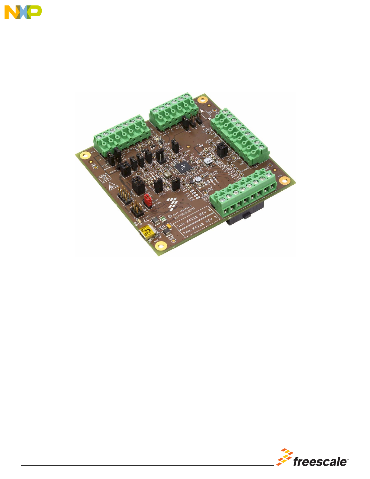
Figure 1. KITVR500EVM
Contents
1 Important Notice . . . . . . . . . . . . . . . . . . . . . . . . . . . . . . . . . . . . . . . . . . . . . . . . . . . . . . . . . . . . . . . . . . . . . . . . . . . . . . . . . . . . . . . . . . . 2
2 Getting Started . . . . . . . . . . . . . . . . . . . . . . . . . . . . . . . . . . . . . . . . . . . . . . . . . . . . . . . . . . . . . . . . . . . . . . . . . . . . . . . . . . . . . . . . . . . . 3
3 Getting to Know the Hardware . . . . . . . . . . . . . . . . . . . . . . . . . . . . . . . . . . . . . . . . . . . . . . . . . . . . . . . . . . . . . . . . . . . . . . . . . . . . . . . . 4
4 Installing the GUI and Setting up the Hardware . . . . . . . . . . . . . . . . . . . . . . . . . . . . . . . . . . . . . . . . . . . . . . . . . . . . . . . . . . . . . . . . . . 13
5 Schematic . . . . . . . . . . . . . . . . . . . . . . . . . . . . . . . . . . . . . . . . . . . . . . . . . . . . . . . . . . . . . . . . . . . . . . . . . . . . . . . . . . . . . . . . . . . . . . . 16
6 Board Layout. . . . . . . . . . . . . . . . . . . . . . . . . . . . . . . . . . . . . . . . . . . . . . . . . . . . . . . . . . . . . . . . . . . . . . . . . . . . . . . . . . . . . . . . . . . . . 21
7 Board Bill of Materials . . . . . . . . . . . . . . . . . . . . . . . . . . . . . . . . . . . . . . . . . . . . . . . . . . . . . . . . . . . . . . . . . . . . . . . . . . . . . . . . . . . . . . 22
8 References . . . . . . . . . . . . . . . . . . . . . . . . . . . . . . . . . . . . . . . . . . . . . . . . . . . . . . . . . . . . . . . . . . . . . . . . . . . . . . . . . . . . . . . . . . . . . . 25
9 Revision History . . . . . . . . . . . . . . . . . . . . . . . . . . . . . . . . . . . . . . . . . . . . . . . . . . . . . . . . . . . . . . . . . . . . . . . . . . . . . . . . . . . . . . . . . . 26
© Freescale Semiconductor, Inc., 2014. All rights reserved.
Page 2

Important Notice
1 Important Notice
Freescale provides the enclosed product(s) under the following conditions:
This evaluation kit is intended for use of ENGINEERING DEVELOPMENT OR EVALUATION PURPOSES ONLY.
It is provided as a sample IC pre-soldered to a printed circuit board to make it easier to access inputs, outputs, and
supply terminals. This evaluation board may be used with any development system or other source of I/O signals
by simply connecting it to the host MCU or computer board via off-the-shelf cables. This evaluation board is not a
Reference Design and is not intended to represent a final design recommendation for any particular application.
Final device in an application will be heavily dependent on proper printed circuit board layout and heat sinking
design as well as attention to supply filtering, transient suppression, and I/O signal quality.
The goods provided may not be complete in terms of required design, marketing, and or manufacturing related
protective considerations, including product safety measures typically found in the end product incorporating the
goods. Due to the open construction of the product, it is the user's responsibility to take any and all appropriate
precautions with regard to electrostatic discharge. In order to minimize risks associated with the customers
applications, adequate design and operating safeguards must be provided by the customer to minimize inherent or
procedural hazards. For any safety concerns, contact Freescale sales and technical support services.
Should this evaluation kit not meet the specifications indicated in the kit, it may be returned within 30 days from the
date of delivery and will be replaced by a new kit.
Freescale reserves the right to make changes without further notice to any products herein. Freescale makes no
warranty, representation or guarantee regarding the suitability of its products for any particular purpose, nor does
Freescale assume any liability arising out of the application or use of any product or circuit, and specifically
disclaims any and all liability, including without limitation consequential or incidental damages. “Typical” parameters
can and do vary in different applications and actual performance may vary over time. All operating parameters,
including “Typical”, must be validated for each customer application by customer’s technical experts.
Freescale does not convey any license under its patent rights nor the rights of others. Freescale products are not
designed, intended, or authorized for use as components in systems intended for surgical implant into the body, or
other applications intended to support or sustain life, or for any other application in which the failure of the Freescale
product could create a situation where personal injury or death may occur.
Should the Buyer purchase or use Freescale products for any such unintended or unauthorized application, the
Buyer shall indemnify and hold Freescale and its officers, employees, subsidiaries, affiliates, and distributors
harmless against all claims, costs, damages, and expenses, and reasonable attorney fees arising out of, directly or
indirectly, any claim of personal injury or death associated with such unintended or unauthorized use, even if such
claim alleges Freescale was negligent regarding the design or manufacture of the part.Freescale™ and the
Freescale logo are trademarks of Freescale Semiconductor, Inc. All other product or service names are the property
of their respective owners.© Freescale Semiconductor, Inc. 2014
2 Freescale Semiconductor, Inc.
KTVR500UG Rev. 1.0 8/2014
Page 3

Getting Started
Jump Start Your Design
2 Getting Started
2.1 Kit Contents/Packing List
The KITVR500EVM contents include:
• Assembled and tested evaluation board/module in anti-static bag.
• Warranty card and Technical support brochure
2.2 Jump Start
Freescale’s analog product development boards help to easily evaluate Freescale products. These tools support analog mixed signal and
power solutions including monolithic ICs using proven high-volume SMARTMOS mixed signal technology, and system-in-package devices
utilizing power, SMARTMOS and MCU dies. Freescale products enable longer battery life, smaller form factor, component count reduction,
ease of design, lower system cost and improved performance in powering state of the art systems.
•Go to www.freescale.com/analogtools
• Locate your kit
• Review your Tool Summary Page
• Look for
• Download documents, software and other information
Once the files are downloaded, review the user guide in the bundle. The user guide includes setup instructions, BOM and schematics.
Jump start bundles are available on each tool summary page with the most relevant and current information. The information includes
everything needed for design.
2.3 Required Equipment and Software
To use this kit, you need:
• Power supply:
• Output voltage range from 3.1 to 4.5 V
• Current capability from 3.0 to 5.0 A (current requirement is dependent on output loading)
• Supply to board connection cables (capable of withstanding up to 5.0 A current)
• USB (male) to mini USB (male) communication cable
• USB-enabled computer
• Multimeter is recommended
2.4 System Requirements
The kit requires the following to function properly with the software:
• Windows XP or Windows 7 operating system
• VR500_GUI_REV_1.1.zip: Graphical User Interface (GUI) for KITVR500EVM
Freescale Semiconductor, Inc. 3
KTVR500UG Rev. 1.0 8/2014
Page 4

Getting to Know the Hardware
3 Getting to Know the Hardware
3.1 Board Overview
The KITVR500EVM evaluation board allows full evaluation capability of the 34VR500 PMIC for the QorlQ LS102x family of application
processors. It provides access to all output voltage rails as well as control and signal pins through terminal block connectors for an easier
out-of-the-box evaluation experience. A single terminal block connector for the input power supply allows the user to supply the board with
an external DC power supply to fully evaluate the performance of the device.
3.2 Board Features
The board features are as follows:
• Input voltage operation range from 3.1 to 4.5 V
• Output voltage supplies accessible through detachable terminal blocks
• Four buck converters
• Five general purpose LDO regulators
• One DDR memory termination voltage reference
• On/off push button support
• Hardware configuration flexibility through various jumper headers and resistors
• Integrated USB to I2C programming interface for full control/configuration
• Onboard PMIC control through the I2C register map
• On board connectors for interfacing with future evaluation/debug tools
• Compact form factor (4 x 4 in2)
3.3 Device Features
This evaluation board features the following Freescale products:
Table 1. Features
Device Description Features
• Four buck converters
Multi-output DC/DC Regulator for QorIQ LS1
MC34VR500
MC9S08JM60 8-bit USB Cost-Effective JM MCUs
Family of Communications Processors
• Five general purpose linear regulators
• Programmable output voltage, sequence, and timing
• DDR termination reference voltage
• Power control logic with processor interface and event detection
• Individually programmable ON, OFF, Standby, and Sleep modes
• 8-bit HCS08 Central Processing Unit (CPU)
• Up to 24 MHz internal bus (48 MHz HCS08 core) frequency offering 2.7
to 5.5 V across temperature range of -40 °C to +85 °C
• Support for up to 32 peripheral interrupt/reset sources
• On-chip Memory
• Up to 60 k flash read/program/erase over the full operating voltage and
temperature
• Up to 4.0 k RAM
• 256 Byte USB RAM
• Support for up to 32 peripheral interrupt/reset sources
4 Freescale Semiconductor, Inc.
KTVR500UG Rev. 1.0 8/2014
Page 5
3.4 Board Description
LDO’s
outputs
Buck regulators
outputs
Power
supply
Logic and
monitoring outputs
PC
interface
via the
USB bus
Power
Management
Figure 2 describes the main blocks of the KITVR500EVM.
Getting to Know the Hardware
Table 2. Board Description
Name Summary Description
Power Supply Main power supply connection (3.1 to 4.5 V)
Logic and monitoring outputs I2C, INTB, EN, PORB and STBY connections for monitoring
LDO’s outputs LDO1, 2, 3, 4, 5 REFOUT output connections (can be used to connect a load)
Buck regulators outputs SW1, 2, 3, 4 output connections (can be used to connect a load)
PC Interface To be connected to the PC running the GUI
Figure 2. Board Description
Freescale Semiconductor, Inc. 5
KTVR500UG Rev. 1.0 8/2014
Page 6
Getting to Know the Hardware
KITVR500EVM
3.5 Jumper Description
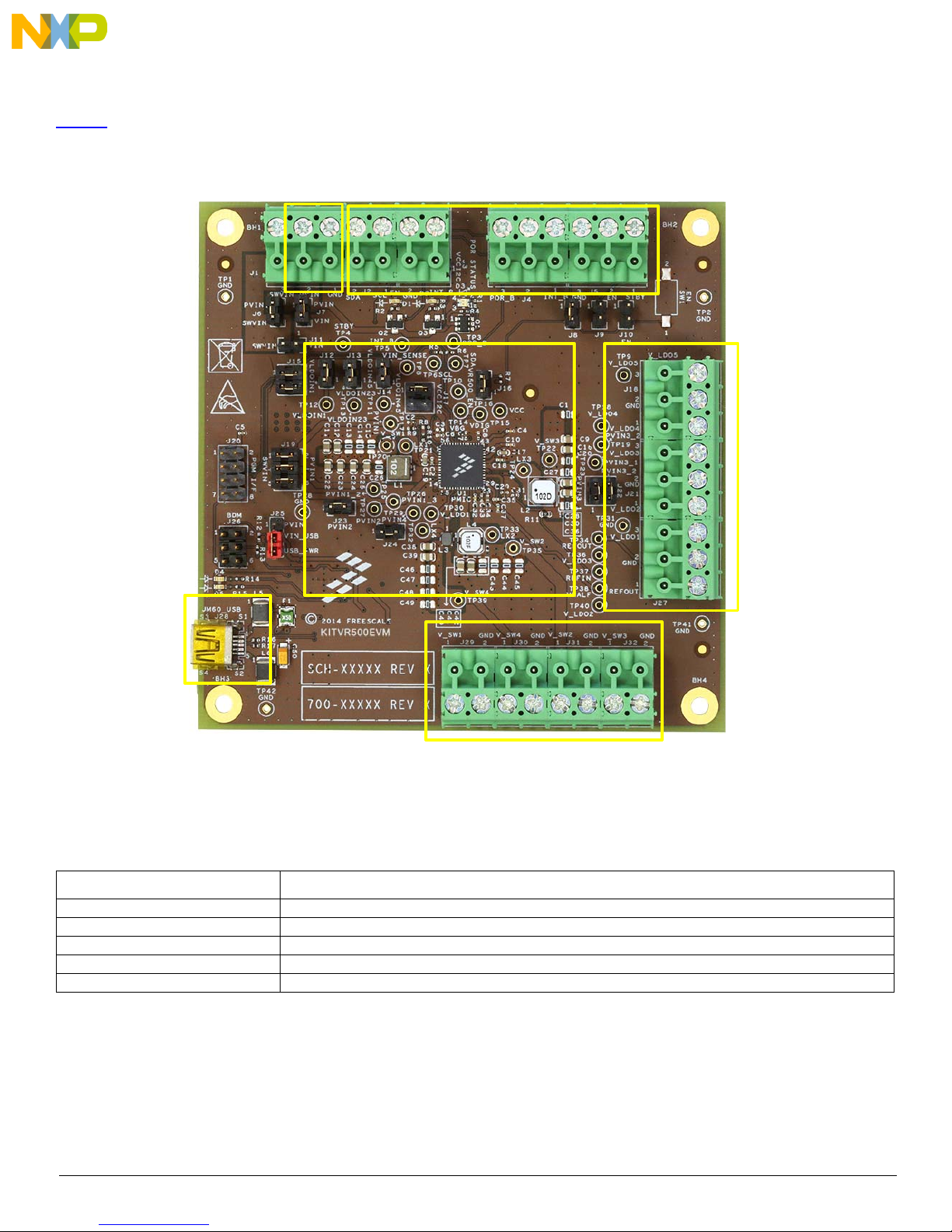
Verify that the jumpers are placed in the right position as shown in Figure 3. For a detailed description of the jumper functionality, refer to
Table 3.
Figure 3. Default Jumper Configuration Diagram
6 Freescale Semiconductor, Inc.
KTVR500UG Rev. 1.0 8/2014
Page 7
Table 3. Jumper Description
Jumper Default Description
Getting to Know the Hardware
J6 Closed
J7 Closed Shorts PVIN to VIN. Allows one to isolate or connect the 34VR500 logic input supply to PVIN net. (debugging option)
J8 Closed Short EN to the MCU
J9 Open Short to pull STBY to PVIN voltage supply
J10 Open Short to hold EN pin low
J11 Open
J12, J13, J14 Closed Short to connect VLDOIN to VIN
J15 Closed Short to connect SCL and SDA to the MCU
J16 Closed Short to connect EN to PVIN
J17 1 - 2
J19, J23, J24
J22
J25 2 - 3
Closed
1 - 2
3 - 4
Shorts PVIN and SWVIN. Allows supply isolation to provide more accurate efficiency readings on the switching
supplies
Shorts SWVIN to VIN. Allows one to isolate or connect the 34VR500 logic input supply to SWVIN net. (debugging
option)
VCCI2C Supply selector
• 1-2: Connect VCCI2C to 3V3 LDO
• 3-4: Connect VCCI2C to SW2 output
Buck regulators input power path isolation
Short these jumpers to allow PVINx to be powered from the SWVIN supply
Buck regulators input power path isolation
Control Interface input supply selector
• 1-2: Enables PVIN node as the input supply source for the control interface
• 2-3: Enables USB power as the input supply source for the control interface
3.6 Connectors and Terminal Blocks Description
Table 4 presents pin connection for each header present on the KITVR500EVM.
Table 4. Terminal Blocks Descriptions
Terminal Block Function Pin definition
J1 Main Input Supply
J2 I²C Signals
J3 VCCI2C
J4 Interfacing 1
J5 Interfacing 2
J18 LDO4 / LDO5
J21 LDO2 / LDO3
J27 REFOUT / LDO1
J29 SW1
Pin 1 – GND
Pin 2 – PVIN
Pin 3 – SWVIN
Pin 1 – SCL
Pin 2 – SDA
Pin 1 – VCCI2C
Pin 2 – GND
Pin 1 – INT_B
Pin 3 – POR_B
Pin 1 – STBY
Pin 2 – EN
Pin 3 – GND
Pin 1 – LDO4 Output
Pin 2 – GND
Pin 3 – LDO5 Output
Pin 1 – LDO2 Output
Pin 2 – GND
Pin 3 – LDO3 Output
Pin 1 – REFOUT Output
Pin 2 – GND
Pin 3 – LDO1 Output
Pin 1 – SW1 Output
Pin 2 – GND
Freescale Semiconductor, Inc. 7
KTVR500UG Rev. 1.0 8/2014
Page 8

Getting to Know the Hardware
Table 4. Terminal Blocks Descriptions (continued)
J30 SW4
J31 SW2
J32 SW3
Table 5. Connector Description
Connector Function Pin definition
J20 Debug Port 1 Debugging connector for future development tools
J26 BDM Connector
J28 Mini USB Connector
J33 Debug Port 2 Debugging connector for future development tools
J34 Debug Port 3 Debugging connector for future development tools
J35 Debug Port 4 Debugging connector for future development tools
Pin 1 – SW4 Output
Pin 2 – GND
Pin 1 – SW2 Output
Pin 2 – GND
Pin 1 – SW3 Output
Pin 2 – GND
Pin 1 - BKGD_JM60
Pin 2 - GND
Pin 3 - NC
Pin 4 - RST_JM60
Pin 5 - NC
Pin 6 - USB_PWR
Pin 1 - VBUS
Pin 2 - DPin 3 - D+
Pin 4 - NC
Pin 5 - GND
Chassis - GND
3.6.1 LDO Input Supply Source Selection
It is possible to modify the LDO input supply sources by removing the Jumpers J12, J13, J14, J17 and connecting another power supply,
as one of the buck converters outputs.
LDO INPUT SENSE POINTS
TP11
TP13
DNP
C33
1.0UF
C35
0.1UF
C37
0.1UF
VHALF
TP12
DNP
TP37
REFIN
TP38
VHALF
C63
1.0UF
DNP
DNP
VLDOIN1
VLDOIN23
VLDOIN45
17
27
40
30
29
U1B
VLDOIN1
VLDOIN23
VLDOIN45
REFIN
VHALF
LDO
REF
REG
MC34VR500V1ES
LDO1
LDO2
LDO3
LDO4
LDO5
REFOUT
V_LDO1
18
V_LDO2
26
V_LDO3
28
V_LDO4
39
V_LDO5
41
31
REFOUT
VIN
J12
2
1
HDR 1X2 TH
J13
2
1
HDR 1X2 TH
J14
1
2
HDR 1X2 TH
Default:
1-2 shunt
V_SW3
VLDOIN45 VLDOIN23 VLDOIN1
DNP
C54
1.0UF
0
R11
REFIN
C31
1.0UF
Figure 4. LDO Schematic Configuration
LDO OUTPUT SENSE POINTS
TP30
V_LDO1 V_LDO2 V_LDO3 V_LDO4 V_LDO5
DNP
C62
4.7uF
TP34
REFOUT
DNP
C29
1.0UF
TP40
DNP
C32
2.2UF
REFOUT
TP36
DNP
C34
4.7uF
TP18
DNP
C10
2.2UF
TP9
DNP
C4
2.2UF
V_LDO1 V_LDO2
V_LDO3 V_LDO4
V_LDO5
8 Freescale Semiconductor, Inc.
KTVR500UG Rev. 1.0 8/2014
Page 9
Getting to Know the Hardware
VIN_SENSE
VDIG
VBG
VCC
LCSADS
Default:
1-2 shunt
Default:
1-2 shunt,
3-4 shunt.
POR_B STBY
INT_B
VR500_EN
Default:
1-2 shunt
Default:
No shunt
Default:
No shunt
Default:
1-2 shunt
VIN
VCC
VBIAS
VBG
VDIG
VCCI2C
I2C_S CL
I2C_S DA
MCU_SDA
MCU_SCL
STBY
INT_ B
POR_B
EN
VR500_EN
VIN
V_SW2
VCCI2C
VCCI2C
PVIN
3V3
PVIN
MCU_SCL3,5
MCU_SDA3,5
STBY 3
INT_ B 3
POR_B 3
EN 3,5
J16
HDR 1X2 TH
1 2
SW1
FSMSM
DNP
12
TP4
DNP
C8
0.47uF
TP6
DNP
TP16
DNP
R7
1M
C51
1.0UF
Control
MC34VR500V1ES
U1A
ICTEST1
5
INT
1
POR
3
SCL
54
SDA
53
STBY
4
VDIG
51
VBG
52
VCCI2C
55
ICTEST2
47
EN
56
VCC
49
VIN
50
VBIAS
43
TP10
DNP
J9
HDR 1X2 TH
1 2
TP14
DNP
J15
HDR 2X2
1 2
3
4
C3
1.0UF
DNP
TP15
DNP
TP8
DNP
R10
10.0K
R6
4.7K
R8
10.0K
R9
100K
C52
1.0UF
R5
4.7K
J10
HDR 1X2 TH
1 2
C53
0.22uF
TP7
DNP
C2
1.0UF
C7
1.0UF
J17
HDR 2X2
1 2
3
4
C6
0.1UF
TP5
DNP
TP3
DNP
J8
HDR 1X2 TH
12
Figure 5. Logic and Core Supplies Schematic
Freescale Semiconductor, Inc. 9
KTVR500UG Rev. 1.0 8/2014
Page 10

Getting to Know the Hardware
STBY
INTB
PORB
SW1
LDO1
SW2
SW4
LDO2
REFOUT
LDO3
SW3
LDO4
LDO5
VCC
VDIG
VBG
EN
Table 6. LDO Input Supply Configuration Chart
Input Pin Input options
VLDOIN1
VLDOIN23
VLDOIN45
REFIN
VCCI2C
Input supply for LDO1:
J12 Closed: VIN
J12 Open: User's choice
Input supply for LDO2 and LDO3:
J13 Closed: VIN
J13 Open: User's choice
Input supply for LDO4 and LDO5:
J14 Closed: VIN
J14 Open: User's choice
Input supply for REFOUT:
R11 = V_SW3
R11 removed: User's choice
Input supply for VCCI2C:
1 - 2: 3V3
3 - 4: V_SW2
3.6.2 Test point
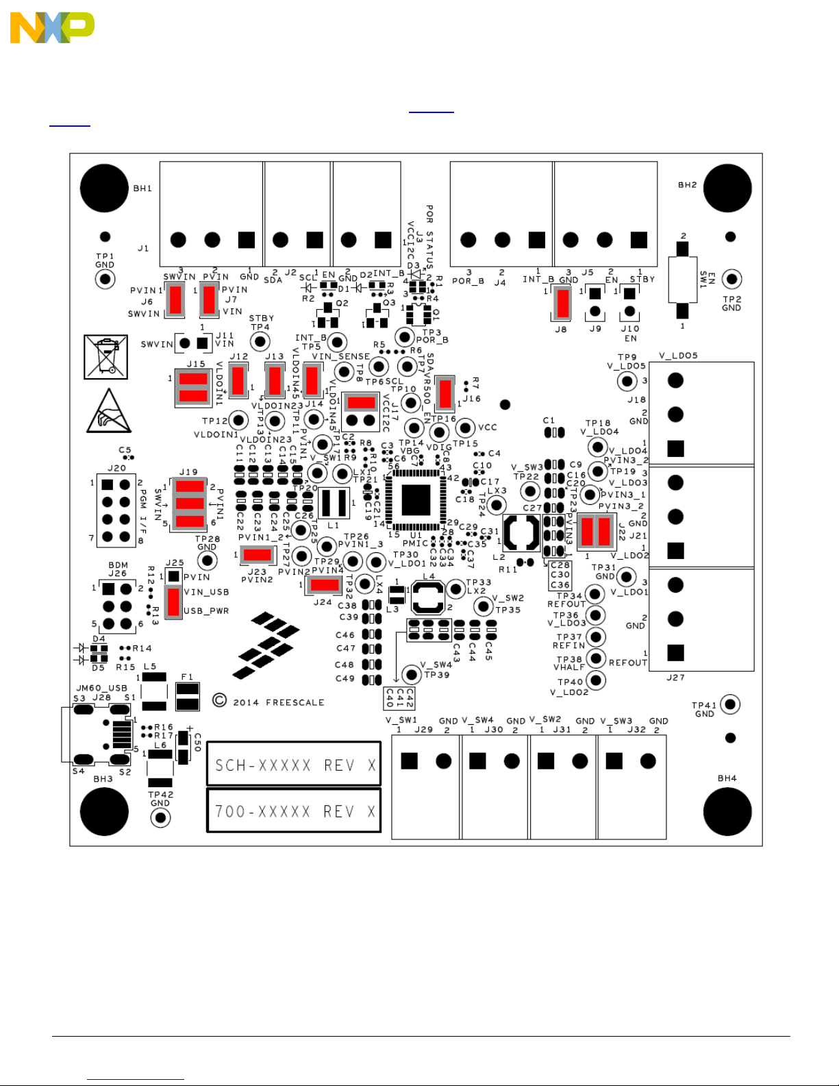
All test points are clearly marked on the evaluation board. Figure 6 shows the location of various test points of interest during evaluation.
Figure 6. Key Test Point Locations
KTVR500UG Rev. 1.0 8/2014
10 Freescale Semiconductor, Inc.
Page 11

Getting to Know the Hardware
VIN_SENSE
VDIG
VBG
VCC
LCSADS
Default:
1-2 shunt
Default:
1-2 shunt,
3-4 shunt.
POR_B STBY
INT_B
VR500_EN
Default:
1-2 shunt
Default:
No shunt
Default:
No shunt
Default:
1-2 shunt
VIN
VCC
VBIAS
VBG
VDIG
VCCI2C
I2C_S CL
I2C_S DA
MCU_SDA
MCU_SCL
STBY
INT_ B
POR_B
EN
VR500_EN
VIN
V_SW2
VCCI2C
VCCI2C
PVIN
3V3
PVIN
MCU_SCL3,5
MCU_SDA3,5
STBY 3
INT_ B 3
POR_B 3
EN 3,5
J16
HDR 1X2 TH
1 2
SW1
FSMSM
DNP
12
TP4
DNP
C8
0.47uF
TP6
DNP
TP16
DNP
R7
1M
C51
1.0UF
Control
MC34VR500V1ES
U1A
ICTEST1
5
INT
1
POR
3
SCL
54
SDA
53
STBY
4
VDIG
51
VBG
52
VCCI2C
55
ICTEST2
47
EN
56
VCC
49
VIN
50
VBIAS
43
TP10
DNP
J9
HDR 1X2 TH
1 2
TP14
DNP
J15
HDR 2X2
1 2
3
4
C3
1.0UF
DNP
TP15
DNP
TP8
DNP
R10
10.0K
R6
4.7K
R8
10.0K
R9
100K
C52
1.0UF
R5
4.7K
J10
HDR 1X2 TH
1 2
C53
0.22uF
TP7
DNP
C2
1.0UF
C7
1.0UF
J17
HDR 2X2
1 2
3
4
C6
0.1UF
TP5
DNP
TP3
DNP
J8
HDR 1X2 TH
12
3.7 Miscellaneous Components
3.7.1 Power on Push Button
A footprint for a normally open, momentary push-button is provided at the EN terminal to allow a momentary low state by pressing the
push button. J8 allows isolation of the EN terminal from the MCU GPIO controlling this pin.
Freescale Semiconductor, Inc. 11
Figure 7. Power on Circuit
KTVR500UG Rev. 1.0 8/2014
Page 12

Getting to Know the Hardware
ROTACI
DNI NWODTUHS
ROTACI
DNI TPURRETNI
INT_B
EN
INT _B
EN
PVIN
PVIN
3B
_
TNI 5,3NE
R2
200 OHM
Q2
FDV302P
1
3 2
D1
LED Red
AC
Q3
FDV302P
1
3 2
D2
LED Red
AC
R3
200 OHM
3.7.2 PMIC LED Indicators
LED indicators are provided to notify the PMIC status to the user. Figure 8 shows the PMIC status LEDs D2 and D4, and a Reserved
LED indicator D3, that allows for an external rework connection to the transistor gate if any given signal debug is required.
RESET INDICATOR
PVIN
3
POR_B
POR_B
3
1
Q1
G
G
FDC6327C
2
S
4
D
6
D
200 OHM
5
S
PVIN
R1
R4
200 OHM
13
D3
LED_RED-GRN
POR_B
Red
Grn
4 2
Table 7 describes the meaning of the LED state.
Table 7. LED State Description
LED Description
Interrupt Notification
D2
D3
D1
ON = PMIC has detected an unmasked interrupt
OFF = No interrupt detected
PORB Notification
Green = PMIC is in regulation and operating properly
Red = PMIC is out of regulation
Reserved debug LED
ON = Q3 gate (R84 pad) is low
OFF = Q3 gate (R84 pad) is high or floating
Figure 8. PMIC Status Indicators
12 Freescale Semiconductor, Inc.
KTVR500UG Rev. 1.0 8/2014
Page 13

Installing the GUI and Setting up the Hardware
4 Installing the GUI and Setting up the Hardware
4.1 Installing the GUI Interface
The new “driverless” environment allows automatically detecting and recognizing the board connected through the USB port, enabling the
specific features and controls for each board.
1. Create a directory on your PC as follows: C:\Freescale\KITVR500GUI
2. Extract the KITVR500GUI.zip file into that directory.
3. Launch the "setup.exe" program.
4. When the following popup dialog appears, click the “Install” button.
Figure 9. KITVR500EVM Installation Window
Freescale Semiconductor, Inc. 13
KTVR500UG Rev. 1.0 8/2014
Page 14

Installing the GUI and Setting up the Hardware
4.2 Configuring the Hardware
The KITVR500EVM operates with a single power supply from 3.1 to 4.5 V and is controlled via USB with help of an integrated USB-I2C
communication bridge. By applying the input voltage supply, the KITVR500EVM powers up according to the default power-up sequence
(34VR500V1) described in the MC34VR500 Data Sheet.
Connect the power supply and the USB communication cables as shown in Figure 10. Multimeter is optional but it is recommended in
order to accurately verify that each one of the output supplies is providing the correct voltage level.
The KITVR500EVM allows the selection of SW2 regulator output or an external 3.3 V LDO
output as the VCCI2C/I2C pull-up supply. By default, the 3.3 V LDO regulator is the source
for the VDDIO supply (J17 = 1–2). If the SW2 regulator is to be set below 3.0 V then make
sure the 3.3 V LDO output is connected to VCCI2C.
14 Freescale Semiconductor, Inc.
Figure 10. KITVR500EVM Board Setup
Note:
KTVR500UG Rev. 1.0 8/2014
Page 15

Installing the GUI and Setting up the Hardware
4.2.1 Step-by-step Instructions for Setting up the Hardware using GUI
To perform the demonstration examples, the following connections and setup must be performed:
1. Connect the power supply to J1, PVIN, and GND pins.
2. Switch on the power supply with a voltage set up between 3.1 and 4.5 V.
3. Connect the mini USB cable to J28 and to the computer.
4. Launch the VR500GUI, the description on how to use the GUI is provided in KTVR500SWUG
Figure 11. KITVR500GUI
The main features of the KITVR500GUI are:
• Automatic detection of the KITVR500EVM
• Read/write access to the 34VR500 PMIC
• Intuitive interface for controlling the 34VR500
• Monitoring all interrupts manually or continuously
• Scrip editor for prototyping, test emulation, or customized operation of the 34VR500 device
• Saving and recalling customized scripts files
KTVR500UG Rev. 1.0 8/2014
Freescale Semiconductor, Inc. 15
Page 16

Schematic
VIN_SENSE
VDIG
VBG
VCC
LCSADS
Default:
1-2 shunt
Default:
1-2 shunt,
3-4 shunt.
POR_B STBY
INT_B
VR500_EN
Default:
1-2 shunt
Default:
No shunt
Default:
No shunt
Default:
1-2 shunt
VIN
VCC
VBIAS
VBG
VDIG
VCCI2C
I2C_S CL
I2C_S DA
MCU_SDA
MCU_SCL
STBY
INT_ B
POR_B
EN
VR500_EN
VIN
V_SW2
VCCI2C
VCCI2C
PVIN
3V3
PVIN
MCU_SCL3,5
MCU_SDA3,5
STBY 3
INT_ B 3
POR_B 3
EN 3,5
J16
HDR 1X2 TH
1 2
SW1
FSMSM
DNP
12
TP4
DNP
C8
0.47uF
TP6
DNP
TP16
DNP
R7
1M
C51
1.0UF
Control
MC34VR500V1ES
U1A
ICTEST1
5
INT
1
POR
3
SCL
54
SDA
53
STBY
4
VDIG
51
VBG
52
VCCI2C
55
ICTEST2
47
EN
56
VCC
49
VIN
50
VBIAS
43
TP10
DNP
J9
HDR 1X2 TH
1 2
TP14
DNP
J15
HDR 2X2
1 2
3
4
C3
1.0UF
DNP
TP15
DNP
TP8
DNP
R10
10.0K
R6
4.7K
R8
10.0K
R9
100K
C52
1.0UF
R5
4.7K
J10
HDR 1X2 TH
1 2
C53
0.22uF
TP7
DNP
C2
1.0UF
C7
1.0UF
J17
HDR 2X2
1 2
3
4
C6
0.1UF
TP5
DNP
TP3
DNP
J8
HDR 1X2 TH
12
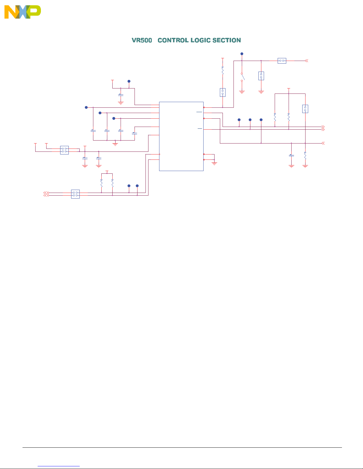
5 Schematic
LDO INPUT SENSE POINTS
TP11
TP13
DNP
C33
1.0UF
C35
0.1UF
C37
0.1UF
VHALF
TP12
DNP
TP37
REFIN
TP38
VHALF
C63
1.0UF
DNP
DNP
VLDOIN1
VLDOIN23
VLDOIN45
17
27
40
30
29
U1B
VLDOIN1
VLDOIN23
VLDOIN45
REFIN
VHALF
LDO
REF
REG
MC34VR500V1ES
LDO1
LDO2
LDO3
LDO4
LDO5
REFOUT
V_LDO1
18
V_LDO2
26
V_LDO3
28
V_LDO4
39
V_LDO5
41
31
REFOUT
VIN
J12
2
1
HDR 1X2 TH
J13
2
1
HDR 1X2 TH
J14
1
2
HDR 1X2 TH
Default:
1-2 shunt
V_SW3
VLDOIN45 VLDOIN23 VLDOIN1
DNP
C54
1.0UF
0
R11
REFIN
C31
1.0UF
LDO OUTPUT SENSE POINTS
TP30
V_LDO1 V_LDO2 V_LDO3 V_LDO4 V_LDO5
DNP
C62
4.7uF
TP34
REFOUT
DNP
C29
1.0UF
TP40
DNP
C32
2.2UF
REFOUT
TP36
DNP
C34
4.7uF
TP18
DNP
C10
2.2UF
TP9
DNP
C4
2.2UF
V_LDO1 V_LDO2
V_LDO3 V_LDO4
V_LDO5
16 Freescale Semiconductor, Inc.
Figure 12. Evaluation Board Schematic, Part 1
KTVR500UG Rev. 1.0 8/2014
Page 17

Schematic
VR500 - CONTROL SIGNALS
TERMINAL BLOCK SECTION
GND
EN
STBY
POR_B
INT _B
5,3
NE
3Y
BT
S
POR_B3
3B_
TNI
J4
SUB_TB_3X1
1
2
3
J5
SUB_TB_3X1
1
2
3
ROTACI
DNI NWODTUHS
ROTACI
DNI TPURRETNI
INT_B
EN
INT _B
EN
PVIN
PVIN
3B
_
TNI 5,3NE
R2
200 OHM
Q2
FDV302P
1
3 2
D1
LED Red
AC
Q3
FDV302P
1
3 2
D2
LED Red
AC
R3
200 OHM
RESET INDICATOR
POR_B
POR_B
PVIN
PVIN
POR_B
3
Red
Grn
D3
LED_RED-GRN
4 2
13
R4
200 OHM
G
D
S
G
S
D
Q1
FDC6327C
2
6
1
5
4
3
R1
200 OHM
VR500 - LDO & REFOUT O/P HEADER SECTION
V_LDO1
V_LDO2
V_LDO3
V_LDO4
V_LDO5
REFOUT
V_LDO1 V_LDO2 V_LDO3 V_LDO4
V_LDO5 REFOUT
J34
CON_2X10
1
2
3 4
65
7 8
9 10
11 12
13 14
15 16
17 18
19 20
SWVIN
PVIN
GND
SUB_TB_3X1
J1
SWVIN PVIN SWVIN
3
2
1
Main Input supply to the board
VR500 Swithcing Regulator input
VR500 Main chip supply &
Supply
PVIN -
SWVIN -
VIN -
Input supply for LDO.
J6
HDR 1X2 TH
Default:
1 2
1-2 shunt
Input Terminal Block J1 pin 2
Input Terminal Block J1 pin 3
(or)
Feed the power from PVIN
by shunting the head er J6.
Feed the power from PVIN
by shunting the head er J7
(or)
Feed the power from SWVIN
by shunting the head er J11.
Default:
No shunt
J11
12
HDR 1X2 TH
Input Source
VIN
1 2
J7
HDR 1X2 TH
Default:
1-2 shunt
3,5
MCU_SCL
MCU_SDA3,5
I2C Terminal Blocks
MCU_SCL
MCU_SDA
1
2
VCCI2C
1
VCCI2C
2
GND
J2
SUB_TB_2X1
J3
SUB_TB_2X1
Freescale Semiconductor, Inc. 17
Figure 13. Evaluation Board Schematic, Part 2
KTVR500UG Rev. 1.0 8/2014
Page 18

Schematic
GND GND GND GND GND GND
GROUND TEST POINTS
TP31
DNP
TP42
DNP
TP28
DNP
TP2
DNP
TP1
DNP
TP41
DNP
3YBTS
VR500 - CONTROL/I2C SIGNALS HEADER
J33
STBY EN
V_LDO1
1
3 4
7 8
9
11 12
13
15 16
17 18
19 20
CON_2X10
REFOUT
2
INT _B
65
POR_B
10
VCCI2C
MCU_SCL
14
MCU_SDA
PVIN
SWVIN
VR500 - LDO & REFOUT O/P
TERMINAL BLOCK SECTION
J27
REFOUT
GND
V_LDO1
1
2
3
SUB_TB_3X1
EN 3,5
INT _B 3
POR_B 3
MCU_SCL 3,5
MCU_SDA 3,5
REFOUT= DDR memory reference
voltage,10 mA.
VCCI2C
V_LDO1= 0.80 to 1.55 V, 250 mA
PVIN SWVIN
V_LDO3 V_LDO2
V_LDO5 V_LDO4
V_LDO2
GND
V_LDO3
V_LDO4
GND
V_LDO5
J21
1
2
3
SUB_TB_3X1
J18
1
2
3
SUB_TB_3X1
V_LDO2 = 1.8 to 3.3 V, 100 mA
V_LDO3 = 1.8 to 3.3 V, 350 mA
V_LDO4 = 1.8 to 3.3 V, 100 mA
V_LDO5 = 1.8 to 3.3 V, 200 mA
MOUNTING HOLES
MTG
BH1
MTG
BH3
Figure 14. KITVR500EVM LDO/Control Schematic Part 3
BH4
MTG
BH2
MTG
18 Freescale Semiconductor, Inc.
KTVR500UG Rev. 1.0 8/2014
Page 19

PVIN1_1 PVIN1_2PVIN1_3
Default:
1-2 shunt,
3-4 shunt,
5-6 shunt.
LX1
6.0A
V_SW1
PVIN2
Default:
1-2 shunt
2.4A
LX2
FB1
FB2
V_SW2
PVIN3_1 PVIN3_2
Default:
1-2 shunt,
3-4 shunt.
2.65A
LX3
FB3
V_SW3
PVIN4
Default:
1-2 shunt
2.0A
LX4
FB4
V_SW4
PVIN1_1
PVIN1_2
PVIN1_3
LX1
V_SW1
PVIN2 LX2
V_SW2
PVIN3_2
PVIN3_1
LX3
V_SW3
PVIN4 LX4
V_SW4
SWVIN
V_SW1
SWVIN
V_SW2
SWVIN
V_SW3
SWVIN
V_SW4
C25
22UF
C64
4.7uF
TP27
DNP
TP23
DNP
C61
0.1UF
C21
0.1UF
C9
22UF
C22
22UF
C30
22UF
J19
HDR 2X3
1
2
3 4
6
5
C57
0.1UF
TP19
DNP
C59
0.1UF
C47
22UF
DNP
L1 1uH
1
2
TP39
DNP
L4 1uH
1 2
C66
4.7uF
C58
4.7uF
TP20
DNP
TP24
DNP
C13
22UF
DNP
C24
22UF
C48
22UF
DNP
C36
22UF
DNP
C15
22UF
DNP
C12
22UF
C42
22UF
DNP
C14
22UF
DNP
C46
22UF
DNP
C27
22UF
DNP
C40
22UF
L2 1uH
1
2
TP25
DNP
TP33
DNP
C39
22UF
C65
0.1UF
C43
22UF
DNP
TP22
DNP
C56
4.7uF
C11
22UF
TP21
DNP
C41
22UF
TP26
DNP
TP35
DNP
J24
HDR 1X2 TH
1 2
C49
22UF
DNP
C26
22UF
DNP
C20
22UF
DNP
C23
22UF
C55
0.1UF
C60
4.7uF
L3 1UH
1
2
TP17
DNP
C45
22UF
DNP
J23
HDR 1X2 TH
1 2
C38
22UF
C1
22UF
DNP
C18
0.1UF
TP32
DNP
TP29
DNP
C44
22UF
DNP
J22
HDR 2X2
1
2
3 4
SW2
SW3
SW4
SW1
MC34VR500V1ES
U1C
PVIN1_3
12
SGND1
14
FB3
38
PVIN3_2
37
LX3_2
36
DNC4
33
PVIN3_1
34
LX3_1
35
SGND3
32
FB4
19
PVIN4
20
DNC6
44
DNC7
45
DNC8
46
PVIN1_1
7
LX1_1
8
PVIN1_2
10
LX1_2
9
FB1
13
LX1_3
11
DNC2
6
FB2
25
LX2
22
LX4
21
EPGND57SGND2
15
DNC1
2
DNC5
42
DNC3
16
SGND4
48
PVIN2_1
23
PVIN2_2
24
C19
4.7uF
C16
22UF
C28
22UF
C17
4.7uF
VR500-SWITHCING REGULATOR O/P
TERMINAL BLOCK SECTION
SW1
0.625 to 1.875 V
4.5 A (M ax. Peak)
SW3
0.625 to 1.975 V ,
2.5 A (M ax. Peak)
SW4
1.0 A
operates in VTT mode
provide DDR termination
at 50% of SW3
SW2
0.625 to 1.975V ,
1.0 A (M ax. Peak)
V_SW1
V_SW2
V_SW3
V_SW4
J32
SUB_TB_2X1
1
2
J29
SUB_TB_2X1
1
2
J31
SUB_TB_2X1
1
2
J30
SUB_TB_2X1
1
2
VR500-SWITHCING REGULATOR O/P HDR
V
VOUT = 1.242 X ( (R2/R1) + 1) = 3.3V
R2 = ((VOUT/1.242) -1) X R1
LDO REGULATOR 3.3 V
Layout Note :
Place this LDO section
on the bottom s ide of the PCB.
R1
R2
VIN_USB
LD0_3V3_EN
3V3
LDO_3V3_ADJ
3V3
VIN_USB
3V3
3V3
LD0_3V3_EN
5
R21 12.0K
R22
20K
U3
MIC5205
IN
1
GND
2
ADJ
4
EN
3
OUT
5
C79
1.0UF
C71
470PF
+
C80
2.2UF
C74
2.2uF
DNP
Schematic
Freescale Semiconductor, Inc. 19
Figure 15. KITVR500EVM Switching Regulators Schematic
V_SW4
V_SW2
_SW3
3,5
KTVR500UG Rev. 1.0 8/2014
V_SW1
V_SW1
V_SW4
V_SW2
V_SW3
J35
1 2
3 4
5
7
9
11 12
13 14
15 16
17 18
19 20
CON_2X10
PROGRAMMING INTERFACE
J20
1
MCU_SDA
51OIPG
MCU_SDA
GPIO1
3
7
HDR 2X4
V_SW1
6
8
10
V_SW1
V_SW4
V_SW2
V_SW4
V_SW2
V_SW3
V_SW3
3V3
C5
2
3V3
MCU_SCL
4
65
EN
8
GPIO2
0.1UF
MCU_SCL 3,5
EN 3,5
GPIO2 5
Page 20

Schematic
Default:
2-3 shunt
Ohm
90
Ohm
90
USB SECTION
USB_GND
VUSB
VUSB_L
USB_DN
USB_DP JM60_USB_DP
JM60_USB_DN
USB_PWR
USB_PWR
PVIN
VIN_USB
JM60_USB_DN 5
JM60_USB_DP 5
R16 33
R17 33
L5
HI1812V101R-10
1
2
J25
HDR 1X3
123
GDI+D-DSUBV
USB-MiniB
J28
1
2
3
4
S2
5
S1
S3S4
+
C50
10UF
L6
HI1812V101R-10
1
2
F1
0.5A
12
C73
0.1uF
ESD PROTECTION
ID1
IDO
MCU_SCL
MCU_SDA
D6
ESD9L5.0ST5G
ESD9L5.0ST5G
A C
Layout Note :
Place the ESD diodes on
the bottom si de of the PCB.
5,3NE
MCU_SCL
3,5
C72
MCU_SDA3,5
0.1uF
51OIPG
52OIPG
D7
A C
R20 0
R19 0
RST_JM60_B
BKGD_JM60
ESD9L5.0ST5G
D8
A C
EN
ID1
IDO
MCU_SCL
MCU_SDA
LED INDICATORS
USB_PWR USB_PWR
Y1
12MHz
AC
D5
LED Red
R15
470
C67
12PF
C68
12PF
AC
D4
LED Green
D9
ESD9L5.0ST5G
A C
PTD0GPIO1
PTD1GPIO2
C70
0.1uF
U2
24
PTA0
25
PTA5
26
PTB0/MISO2/ADP0
27
PTB1/MOSI2/ADP1
28
PTB2/SPSCK2/ADP2
29
PTB3/SS2/ADP3
30
PTB4/KBIP4/ADP4
31
PTB5/KBIP5/ADP5
44
PTC0/SCL
45
PTC1/SDA
46
PTC2
47
PTC3/TxD2
1
PTC4
48
PTC5/RxD2
32
PTD0/ADP8/ACMP+
33
PTD1/ADP9/ACMP-
36
PTD2/KBIP2/ACMPO
37
PTD7
2
IRQ/TPMCLK
3
RESET
40
BKGD/MS
MC9S08JM60CGTE
C69
0.1uF
17
34
VDD
PTE2/TPM1CH0
PTE3/TPM1CH1
VDDAD/VREFH
PTF0/TPM1CH2
PTF1/TPM1CH3
PTF4/TPM2CH0
PTF5/TPM2CH1
VSS
VSSAD/VREFL
VSSOSC
GND
18
35
43
49
C76
0.1uF
PTE0/TxD1
PTE1/RxD1
PTE4/MISO1
PTE5/MOSI1
PTE6/SPSCK1
PTE7/SS1
PTF6
PTG0/KBIP0
PTG1/KBIP1
PTG2/KBIP6
PTG3/KBIP7
PTG4/XTAL
PTG5/EXTAL
VUSB33
USBDN
USBDP
VIN_USB
+
C78
10UF
Layout Note :
Place this JM60 MCU
on the bottom si de of the PCB.
9
10
11
LD0_3V3_EN
12
LED_GRN_ON
13
LED_RED_ON
14
15
16
4
5
6
7
8
22
23
38
39
41
42
21
VUSB33
19
20
LD0_3V3_EN 5
VUSB33
C77
0.47UF
VUSB33
R14
470
LED_GRN_ON
LED_RED_ON
XTAL_JM60
EXTAL_JM60
+
C75
4.7UF
CRYSTAL SECTION
12
GND2
R18
GND1
1M
3 4
Layout Note :
Place the crstal section on the
bottom side of the PCB as close
as possible to the JM60 MCU.
BKGD_JM60
20 Freescale Semiconductor, Inc.
Figure 16. KITVR500EVM Control/programming Interface Schematic
BDM PROGRAMMER
USB_PWR USB_PWR
R12
4.7K
J26
1 2
3 4
HDR 2X3
65
USB_PWR
RST_JM60_B
R13
4.7K
KTVR500UG Rev. 1.0 8/2014
R24
R23
1.5K
1.5K
DNP
DNP
90
Ohm
JM60_USB_DN
JM60_USB_DP
JM60_USB_DN 5
JM60_USB_DP 5
Page 21

6 Board Layout
KITVR500EVM
6.1 Silkscreen
Board Layout
Freescale Semiconductor, Inc. 21
KTVR500UG Rev. 1.0 8/2014
Page 22

Board Bill of Materials
7 Board Bill of Materials
Table 8. Bill of Materials
Item Qty Schematic Label Value Description Part Number
Active Components
11U1
21U2
31U3
4 1 Y1 12 MHz
Mounting Hole
54
Capacitors
6
7
8
9
10
11
12
13
14
15
16
17
18
19
20
21
22
23
24
Diodes
25
3 D1,D2,D5 LED Red LED RED SGL 30MA 0603 SML-LXFM0603SIC-TR
26
1 D3
BH1,BH2,BH3,BH4
C1,C13,C14,C15,C20,C
26,C27,C36,C42,C43,C4
16
4,C45,C46,C47,C48,C49
C2,C7,C29,C31,C33,C5
9
1,C52,C54,C63
1 C3 1.0 F CAP CER 1.0 F 10V 10% X5R 0402 CC0402KRX5R6BB105
3 C4,C10,C32 2.2 F CAP CER 2.2 F 6.3 V 20% X5R 0402 C0402C225M9PACTU
C5,C6,C18,C21,C35,C3
11
7,C55,C57,C59,C61,C65
1 C8 0.47 F CAP CER 0.47 F 16 V 10% X5R 0402 C1005X5R1C474K
C9,C11,C12,C16,C22,C
23,C24,C25,C28,C30,C3
14
8,C39,C40,C41
C17,C19,C56,C58,C60,
7
C64,C66
2 C34,C62 4.7 F CAP CER 4.7 F 6.3 V 20% X5R 0402 C0402X5R6R3-475MNP
2 C50,C78 10 F CAP TANT 10 F 16 V 10% -- 3216-18 TAJA106K016R
1 C53 0.22 F CAP CER 0.22 F 16 V 10% X7R 0402 GRM155R71C224KA12D
2 C67,C68 12 PF CAP CER 12 PF 25 V 5% C0G 0402 CC0402JRNPO8BN120
5 C69,C70,C72,C73,C76 0.1 F CAP CER 0.1 F 16 V 10% X5R 0402 C1005X5R1C104K
1 C71 470 PF CAP CER 470 PF 50 V 5% COG 0603 06035A471JAT2A
1 C74 2.2 F CAP CER 2.2 F 16 V 10% X5R 0603 GRM188R61C225KE15D
1 C75 4.7 F CAP TANT 4.7 F 10 V 10% -- 3216-18 T491A475K010AT
1 C77 0.47 F CAP CER 0.47 F 16V 10% X7R 0603 C0603C474K4RAC
1 C79 1.0 F CAP CER 1.0 F 16 V 10% X5R 0603 C1608X5R1C105K
1 C80 2.2 F
(1)
Freescale IC POWER MANAGEMENT
COMMUNICATION -0.3-4.8 V QFN56
Freescale IC MCU 8-bit 48 MHZ 60 KB
FLASH 2.7-5.5V QFN48
Micrel IC LIN VREG LDO 1.5-15 V 150
MA 2.5-16 V SOT23-5
Aker XTAL 12 MHZ 12PF -- 3.2X2.5MM
SMT
MOUNTING HOLE 0.130 INCH, no part
to order
22 F CAP CER 22 F 10 V 20% X5R 0805 LMK212BJ226MG-T
1.0 F CAP CER 1.0 F 10 V 10% X5R 0402 CC0402KRX5R6BB105
0.1 F CAP CER 0.1 F 10 V 10% X5R 0402 C0402C104K8PAC
22 F CAP CER 22 F 10 V 20% X5R 0805 LMK212BJ226MG-T
4.7 F CAP CER 4.7 F 10 V 10% X5R 0603 LMK107BJ475KA-T
CAP TANT ESR=1.800 OHMS 2.2 F
10 V 10% 3216-18
LED_RED-GR
N
LED DUAL GRN/RED 30MA SMT LTST-C195KGJRKT
MC34VR500V1ES
MC9S08JM60CGTE
MIC5205YM5
C3E-12.000-12-3030-R
TPSA225K010R1800
Assy
Opt
(3)
(3)
(3)
(3)
(2)
(2)
(3)
(2)
22 Freescale Semiconductor, Inc.
KTVR500UG Rev. 1.0 8/2014
Page 23

Board Bill of Materials
Table 8. Bill of Materials
(1)
(continued)
Item Qty Schematic Label Value Description Part Number
27
1 D4 LED Green LED GRN SGL 30MA SMT 0603 SML-LXFM0603SUGCTR
28
4 D6,D7,D8,D9
ESD9L5.0ST5GDIODE TVS ESD PROT ULT LOW
CAP 5-5.4V SOD-923
ESD9L5.0ST5G
Resistors
29
30
31
32
33
34
35
36
37
38
39
40
4 R1,R2,R3,R4 200 RES MF 200 1/10W 1% 0402 ERJ2RKF2000X
4 R5,R6,R12,R13 4.7 K RES MF 4.7 K 1/16W 1% 0402 RK73H1ETTP4701F
2 R7,R18
2 R8,R10
1.0 M
10 K
RES MF 1.0 M 1/16W 1% AEC-Q200
0402
RES MF 10 K 1/16W 1% AEC-Q200
0402
CRCW04021M00FKED
CRCW040210K0FKED
1 R9 100 K RES MF 100 K 1/16W 5% 0402 RK73B1ETTP104J
1 R11 ZERO RES MF ZERO 1/10W 1% 0603 MC0603SAF0000T5E
2 R14,R15 470 RES MF 470 1/16W 1% 0402 CR-02FL6--470R
2 R16,R17 33 RES MF 33 1/16W 1% 0402 CR-02FL6---33R
2 R19,R20 ZERO RES MF ZERO 1/10W -- 0402 ERJ-2GE0R00X
1 R21 12 K RES MF 12 K 1/10W 1% 0603 RK73H1JTTD1202F
1 R22 20 K RES MF 20 K 1/10W 5% 0603 CR0603-JW-203ELF
2 R23,R24
1.5 K
RES MF 1.5 K 1/16W 5% 0402 CRCW04021K50JNED
Inductors
41
42
43
44
45
1 L1 1 H
1 L2 1 H
1 L3 1 H
1 L4 1 H
2 L5,L6
HI1812V101R10
Coilcraft IND PWR 1 H@100 KHz 6 A
20% SMT
Coilcraft IND PWR 1 H@100 KHZ
2.65 A 20% SMT
TDK IND PWR 1 H@1 MHZ 2 A 30%
SMT
Coilcraft IND PWR 1 H@100 KHZ 2.4
A 30% SMT
IND FER 100 @100 MHZ 8 A 25%
SMD/1812
XAL4020-102MEC
LPS5015-102MLC
VLS252010T-1R0N
LPS4012-102NLC
HI1812V101R-10
Switches, Connectors, Jumpers, and Test Points
46
1 F1
0.5 A
FUSE PLYSW 0.5A 13.2V SMT MICROSMD050F-2
SUBASSEMBLY HDR 1X3 TH 197MIL
47
6 J1,J4,J5,J18,J21,J27
SUB_TB_3X1
374H SN 138L + CON 1X3 PLUG TB
210-80542,211-79574
TH 5MM 449H
SUBASSEMBLY HDR 1X2 TH 197MIL
48
6 J2,J3,J29,J30,J31,J32
SUB_TB_2X1
374H SN 138L + CON 1X2 PLUG TB
210-80539,211-79573
TH 5MM 449H
49 12
50 3
51 2
52 1
53 1
54 1
J6,J7,J8,J9,J10,J11,J12,
J13,J14,J16,J23,J24
J15,J17,J22
J19,J26
J20
J25
J28
HDR 1X2 TH
HDR 2X2
HDR 2X3
HDR 2X4
HDR 1X3
USB-MiniB
HDR 1X2 TH 100MIL SP 339H AU 118L 210-91-02GB01
HDR 2X2 TH 100MIL CTR 340H SN
105L
HDR 2X3 TH 100MIL CTR 335H AU
95L
HDR 2X4 TH 100MIL CTR 425H AU
310L
5-146258-2
TSW-103-07-S-D
TSW-104-16-G-D
HDR 1X3 TH 100MIL SP 340H AU 118L M20-9990345
CON 5 USB MINI-B RA SHLD SKT
SMT 31MIL SP AU
675031340
Assy
Opt
(2)
(3)
(3)
(3)
(3)
Freescale Semiconductor, Inc. 23
KTVR500UG Rev. 1.0 8/2014
Page 24

Board Bill of Materials
Table 8. Bill of Materials
Item Qty Schematic Label Value Description Part Number
55 3
56 1
57 2
58 1
59 42
Notes
1. Freescale does not assume liability, endorse, or warrant components from external manufacturers are referenced in circuit drawings or tables.
While Freescale offers component recommendations in this configuration, it is the customer’s responsibility to validate their application.
2. Do not populate
3. Critical components. For critical components, it is vital to use the manufacturer listed.
J33,J34,J35
Q1
Q2,Q3
SW1
TP1,TP2,TP3,TP4,TP5,
TP6,TP7,TP8,TP9,TP10,
TP11,TP12,TP13,TP14,
TP15,TP16,TP17,TP18,
TP19,TP20,TP21,TP22,
TP23,TP24,TP25,TP26,
TP27,TP28,TP29,TP30,
TP31,TP32,TP33,TP34,
TP35,TP36,TP37,TP38,
TP39,TP40,TP41,TP42
(1)
(continued)
CON_2X10
FDC6327C
FDV302P
FSMSM
TEST POINT
RED
CON 2X10 SKT SMT 100MIL CTR
390H AU
TRAN MOSFET DUAL N & P
CHANNEL 2.5V S-SOT6
TRAN PMOS SW 120MA 25V SOT23 FDV302P
SW SPST PB 12V 50MA SMT 1437566-4
TEST POINT RED 40 MIL DRILL 180
MIL TH 109L
SSW-110-22-F-D-VS-N
FDC6327C
5000
Assy
Opt
(2)
(2)
24 Freescale Semiconductor, Inc.
KTVR500UG Rev. 1.0 8/2014
Page 25

8 References
Following are URLs where you can obtain information on related Freescale products and application solutions:
References
Freescale.com
Support Pages
KITVR500EVM Tool Summary Page
MC34VR500 Product Summary Page http://www.freescale.com/webapp/sps/site/prod_summary.jsp?code=MC34VR500
KTVR500SWUG Software User Guide
Description URL
http://www.freescale.com/webapp/sps/site/prod_summary.jsp?code=KITVR500EVM
http://cache.freescale.com/files/analog/doc/user_guide/KTVR500SWUG.pdf
8.1 Support
Visit www.freescale.com/support for a list of phone numbers within your region.
8.2 Warranty
Visit www.freescale.com/warranty for a list of phone numbers within your region.
Freescale Semiconductor, Inc. 25
KTVR500UG Rev. 1.0 8/2014
Page 26

Revision History
9 Revision History
Revision Date Description of Changes
1.0
8/2014 • Initial Release
26 Freescale Semiconductor, Inc.
KTVR500UG Rev. 1.0 8/2014
Page 27

How to Reach Us:
Home Page:
freescale.com
Web Support:
freescale.com/support
Information in this document is provided solely to enable system and software implementers to use Freescale products.
There are no express or implied copyright licenses granted hereunder to design or fabricate any integrated circuits based
on the information in this document.
Freescale reserves the right to make changes without further notice to any products herein. Freescale makes no
warranty, representation, or guarantee regarding the suitability of its products for any particular purpose, nor does
Freescale assume any liability arising out of the application or use of any product or circuit, and specifically disclaims any
and all liability, including without limitation consequential or incidental damages. “Typical” parameters that may be
provided in Freescale data sheets and/or specifications can and do vary in different applications, and actual performance
may vary over time. All operating parameters, including “typicals,” must be validated for each customer application by
customer’s technical experts. Freescale does not convey any license under its patent rights nor the rights of others.
Freescale sells products pursuant to standard terms and conditions of sale, which can be found at the following address:
freescale.com/SalesTermsandConditions.
Freescale and the Freescale logo are trademarks of Freescale Semiconductor, Inc., Reg. U.S. Pat. & Tm. Off.
SMARTMOS is a trademark of Freescale Semiconductor, Inc. All other product or service names are the property of their
respective owners.
© 2014 Freescale Semiconductor, Inc.
Document Number: KTVR500UG
Rev. 1.0
8/2014
 Loading...