

Page 1
© Freescale Semiconductor, Inc., 2013. All rights reserved.
Freescale Semiconductor, Inc.
User’s Guide
Document Number: KT912F634UG
Rev. 2.0, 10/2013
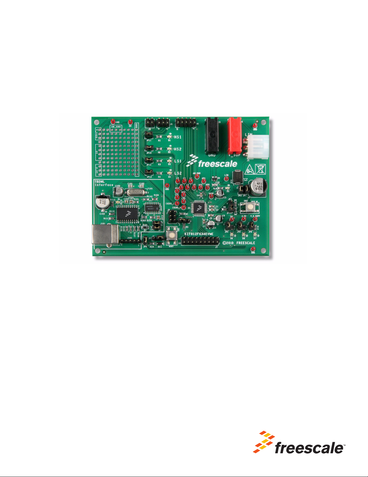
KIT912F634EVME Evaluation Board
Featuring the MM912F634 Integrated S12-Based Relay Driver with LIN Device
Figure 1. KIT912F634EVME Evaluation Board
1 Kit Contents/Packing List . . . . . . . . . . . . . . . . . . . . . . . . . . . . . . . . . . . . . . . . . . . . . . . . . . . . . . . . . . . . . . . . . . . . . . . . . . . . . . . . . . . 2
2 Jump Start . . . . . . . . . . . . . . . . . . . . . . . . . . . . . . . . . . . . . . . . . . . . . . . . . . . . . . . . . . . . . . . . . . . . . . . . . . . . . . . . . . . . . . . . . . . . . . 3
3 Important Notice. . . . . . . . . . . . . . . . . . . . . . . . . . . . . . . . . . . . . . . . . . . . . . . . . . . . . . . . . . . . . . . . . . . . . . . . . . . . . . . . . . . . . . . . . 4
4 KIT912F634EVME Introduction . . . . . . . . . . . . . . . . . . . . . . . . . . . . . . . . . . . . . . . . . . . . . . . . . . . . . . . . . . . . . . . . . . . . . . . . . . . . . 5
5 Required Equipment . . . . . . . . . . . . . . . . . . . . . . . . . . . . . . . . . . . . . . . . . . . . . . . . . . . . . . . . . . . . . . . . . . . . . . . . . . . . . . . . . . . . . 6
6 Setup Guide . . . . . . . . . . . . . . . . . . . . . . . . . . . . . . . . . . . . . . . . . . . . . . . . . . . . . . . . . . . . . . . . . . . . . . . . . . . . . . . . . . . . . . . . . . . . 6
7 Hardware Description. . . . . . . . . . . . . . . . . . . . . . . . . . . . . . . . . . . . . . . . . . . . . . . . . . . . . . . . . . . . . . . . . . . . . . . . . . . . . . . . . . . . . 8
8 Software Description . . . . . . . . . . . . . . . . . . . . . . . . . . . . . . . . . . . . . . . . . . . . . . . . . . . . . . . . . . . . . . . . . . . . . . . . . . . . . . . . . . . . 16
9 Schematics. . . . . . . . . . . . . . . . . . . . . . . . . . . . . . . . . . . . . . . . . . . . . . . . . . . . . . . . . . . . . . . . . . . . . . . . . . . . . . . . . . . . . . . . . . . . 34
10 Board Layout . . . . . . . . . . . . . . . . . . . . . . . . . . . . . . . . . . . . . . . . . . . . . . . . . . . . . . . . . . . . . . . . . . . . . . . . . . . . . . . . . . . . . . . . . 36
11 Bill of Materials . . . . . . . . . . . . . . . . . . . . . . . . . . . . . . . . . . . . . . . . . . . . . . . . . . . . . . . . . . . . . . . . . . . . . . . . . . . . . . . . . . . . . . . . 40
12 References. . . . . . . . . . . . . . . . . . . . . . . . . . . . . . . . . . . . . . . . . . . . . . . . . . . . . . . . . . . . . . . . . . . . . . . . . . . . . . . . . . . . . . . . . . . 43
13 Revision History . . . . . . . . . . . . . . . . . . . . . . . . . . . . . . . . . . . . . . . . . . . . . . . . . . . . . . . . . . . . . . . . . . . . . . . . . . . . . . . . . . . . . . . 44
Page 2

Kit Contents/Packing List
1 Kit Contents/Packing List
• MM912F634 Evaluation Board (EVB)
• Cable, 6FT. USB2.0 A-M to B-M
• Warranty Card, Freescale
KT912F634UG User’s Guide Rev. 2.0 10/2013
2 Freescale Semiconductor, Inc.
Page 3

2Jump Start
Jump Start Your Design
•Go to www.freescale.com/analogtools
• Locate your kit
• Review your Tool Summary Page
• Look for
• Download documents, software and other information
Jump Start
KT912F634UG User’s Guide Rev. 2.0 10/2013
Freescale Semiconductor, Inc. 3
Page 4

Important Notice
3 Important Notice
Freescale provides the enclosed product(s) under the following conditions:
This evaluation kit is intended for use of ENGINEERING DEVELOPMENT OR EVALUATION PURPOSES
ONLY. It is provided as a sample IC pre-soldered to a printed circuit board to make it easier to access inputs,
outputs, and supply terminals. This evaluation board may be used with any development system or other
source of I/O signals by simply connecting it to the host MCU or computer board via off-the-shelf cables. This
evaluation board is not a Reference Design and is not intended to represent a final design recommendation
for any particular application. Final device in an application will be heavily dependent on proper printed circuit
board layout and heat sinking design as well as attention to supply filtering, transient suppression, and I/O
signal quality.
The goods provided may not be complete in terms of required design, marketing, and or manufacturing related
protective considerations, including product safety measures typically found in the end product incorporating
the goods. Due to the open construction of the product, it is the user's responsibility to take any and all
appropriate precautions with regard to electrostatic discharge. In order to minimize risks associated with the
customers applications, adequate design and operating safeguards must be provided by the customer to
minimize inherent or procedural hazards. For any safety concerns, contact Freescale sales and technical
support services.
Should this evaluation kit not meet the specifications indicated in the kit, it may be returned within 30 days from
the date of delivery and will be replaced by a new kit.
Freescale reserves the right to make changes without further notice to any products herein. Freescale makes
no warranty, representation or guarantee regarding the suitability of its products for any particular purpose, nor
does Freescale assume any liability arising out of the application or use of any product or circuit, and
specifically disclaims any and all liability, including without limitation consequential or incidental damages.
“Typical” parameters can and do vary in different applications and actual performance may vary over time. All
operating parameters, including “Typical”, must be validated for each customer application by customer’s
technical experts.
Freescale does not convey any license under its patent rights nor the rights of others. Freescale products are
not designed, intended, or authorized for use as components in systems intended for surgical implant into the
body, or other applications intended to support or sustain life, or for any other application in which the failure
of the Freescale product could create a situation where personal injury or death may occur.
Should Buyer purchase or use Freescale products for any such unintended or unauthorized application, Buyer
shall indemnify and hold Freescale and its officers, employees, subsidiaries, affiliates, and distributors
harmless against all claims, costs, damages, and expenses, and reasonable attorney fees arising out of,
directly or indirectly, any claim of personal injury or death associated with such unintended or unauthorized
use, even if such claim alleges that Freescale was negligent regarding the design or manufacture of the
part.Freescale™ and the Freescale logo are trademarks of Freescale Semiconductor, Inc. All other product or
service names are the property of their respective owners.
© Freescale Semiconductor, Inc. 2013
KT912F634UG User’s Guide Rev. 2.0 10/2013
4 Freescale Semiconductor, Inc.
Page 5

4 KIT912F634EVME Introduction
Freescale Semiconductor’s KIT912F634EVME is a system solution which gives the user the capability to easily
evaluate most of the features provided by the MM912F634 - integrated dual low-side and dual high-side switch
with embedded MCU and LIN transceiver for relay drivers. The MM912F634 features two dice in a single
package. The 16-bit core and the analog die are connected by means of the Die-to-Die interface that provides
direct address access to the registers on the analog die. The analog die contains HS and LS switches, as well
as a PWM module, ADC module, timer module, SCI module, LIN physical interface, and other general registers.
All external signals are accessible via header connectors, and most of the signals can also be checked via test
points. The evaluation module board also includes the TBDML programming/debugging interface, so no
external interface is needed. The board can be powered either from two 4.0
LIN connector. For quick familiarization with the device, a graphical user interface, based on FreeMASTER
software, is provided together with the module. Thanks to the GUI, the user can easily evaluate the peripheral
modules, or directly access the registers on the analog die.
4.1 MM912F634 Features
• 16-Bit S12 CPU, 32 kByte FLASH, 2.0 kByte RAM
• Background Debug (BDM) and Debug Module (DBG)
• Die-to-die bus interface for transparent memory mapping
• On-chip oscillator and two independent watchdogs
• LIN 2.1 physical layer interface with integrated SCI
• Six digital MCU GPIOs shared with SPI (PA5…0)
• 10-bit, 15-channel - Analog-to-Digital Converter (ADC)
• 16-bit, 4-channel - Timer Module (TIM16B4C)
• 8-bit, 2-channel - Pulse Width Modulation module (PWM)
• Six high-voltage/wake-up inputs (L5.0)
• Three low-voltage GPIOs (PB2.0)
• Low power modes with cyclic-sense and forced wake-up
• Current Sense Module with selectable gain
• Reverse-battery-protected Voltage Sense Module
• Two protected low-side outputs to drive inductive loads
• Two protected high-side outputs
• Chip temperature sensor
• Hall sensor supply
• Integrated voltage regulator(s)
KIT912F634EVME Introduction
mm banana connectors or from the
4.2 Caution
1. When working with the kit, always use an isolated laboratory power supply.
2. Keep in mind all ESD rules when handling the board. Avoid touching the connector pins, they are directly
connected to the device pins. Even though the device pins are ESD protected, this protection has its limits.
Some EDS events can destroy or damage the device, or cause its malfunction.
KT912F634UG User’s Guide Rev. 2.0 10/2013
Freescale Semiconductor, Inc. 5
Page 6
Required Equipment
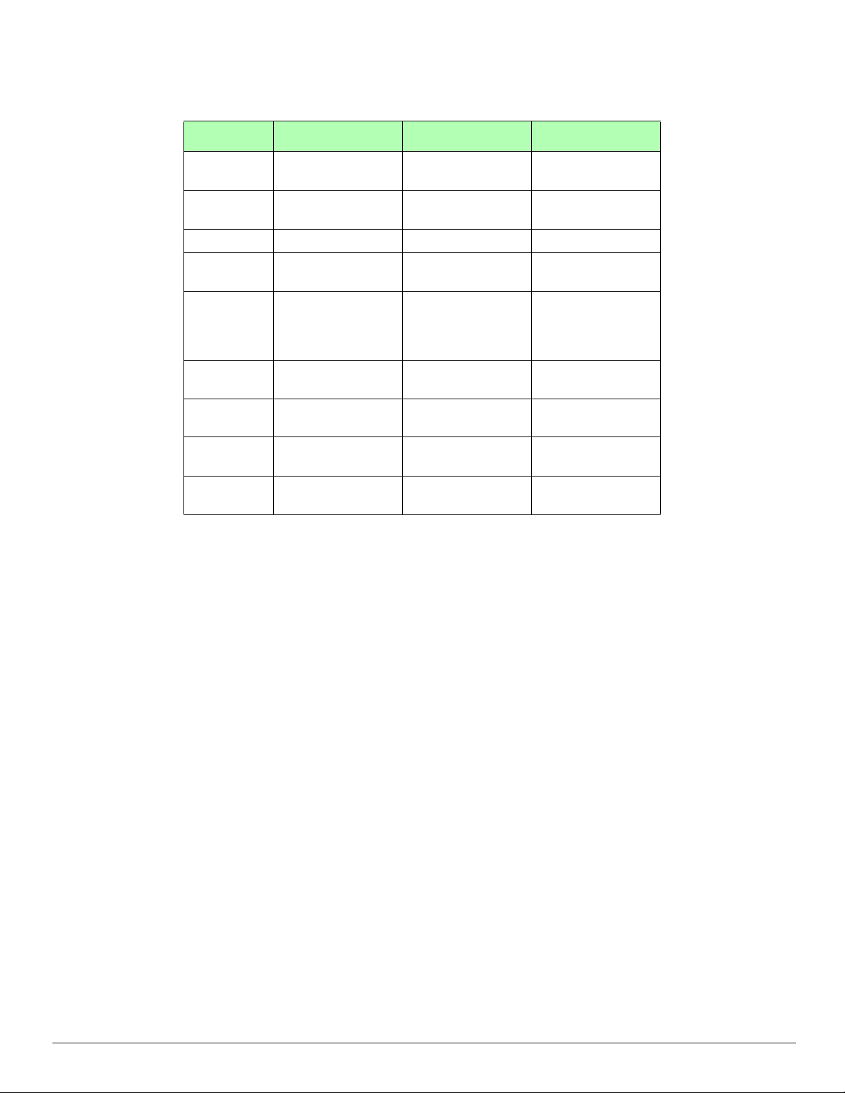
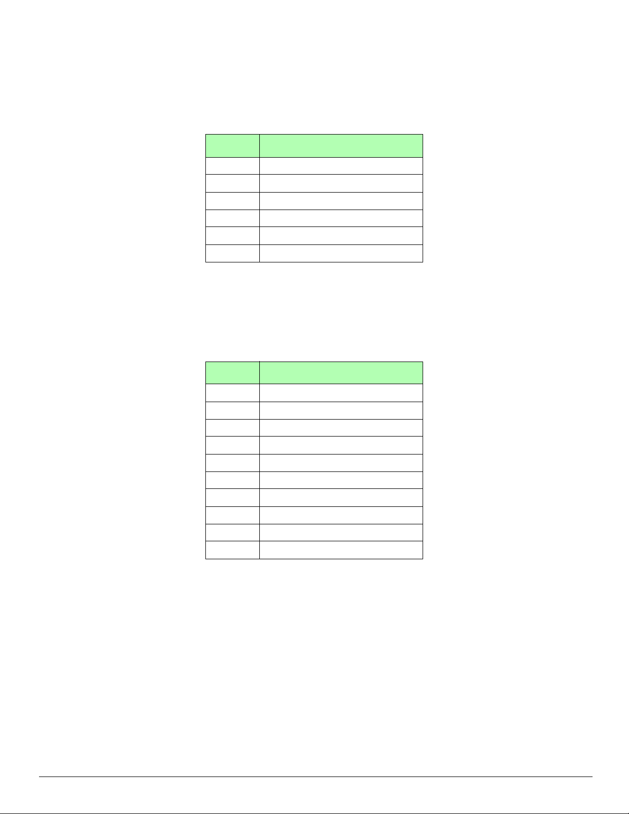
4.3 Acronyms
Acronym Meaning Acronym Meaning
Tabl e 1. Explanation of Acronyms
D2D Die to Die bus
interface
BDM Background Debug
Module
EVB Evaluation Board LED Light Emitting Diode
EVM Evaluation Module LIN Local Interconnect
ESD Electrostatic
Discharge,
Electrostatic Sensitive
Device
GND In this document: main
supply ground
GPIO General Purpose
Input/Output
GUI Graphical User
Interface
ADC Analog to Digital
Converter
5 Required Equipment
• PC Computer running Windows XP or higher
• 12V Power Supply
• USB Cable (supplied)
MCU Microcontroller Unit
HS High Side (switch)
Network
LS Low Side (switch)
PWM Pulse Width
Modulation
SCI Serial Communication
Interface
TBDML Turbo BDM Lite
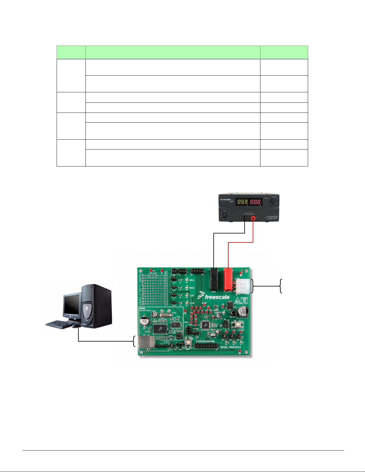
6 Setup Guide
6.1 Hardware Setup
Setup and connections for the KIT912F634EVME are straightforward.
The KIT912F634EVME requires a connection to the power supply and a connection to the PC or notebook via
the USB cable.
Follow these steps to set up the board:
1. Plug the USB cable into the connector J101 and connect the other end of the cable to the PC or notebook.
2. A basic jumper configuration is required to be able to use the KIT912F634EVME. See Table 2 for details.
Table 3 provides a complete index of jumper settings.
3. Connect a laboratory power supply via banana connectors to the board, using J2 (V_S supply) and J3
(GND). Alternatively, the LIN connector can be used for powering the board. The supply voltage has to be
in the range of 8.0 to 18
(+5.0
JP8, JP9 are closed.
6 Freescale Semiconductor, Inc.
Figure 2 depicts a complete setup.
V. When power is applied to the KIT912F634EVME, the green power-on LEDs D6
V), D7 (supply), and D8 (+2.5 V) are lit when power is present and the corresponding jumpers JP4,
KT912F634UG User’s Guide Rev. 2.0 10/2013
Page 7
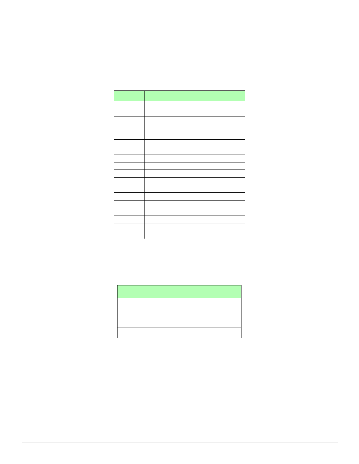
Tab l e 2. KIT912F634EVMEJumper Options for Basic Functionality
Power Supply
GND
V_SUP
USB
(+12 V)
Optional
LIN Connector
Power
Jumper Function Connections
Setup Guide
JP1 Supplying of the device logic (VDDX regulator) and Hall sensor supply
closed
regulator enabled
Supplying of the device logic (VDDX regulator) and Hall sensor supply
open
regulator disabled
JP2 Supplying of the HS drivers enabled closed
Supplying of the HS drivers disabled open
JP14 BDM signal from TBDML interface enabled closed
BDM signal from TBDML interface disabled, external BDM interface can
open
be used (connected to J4)
JP15 RST signal from TBDML interface enabled closed
RST signal from TBDML interface disabled, external BDM interface can
open
be used (connected to J4)
Figure 2. KIT912F634EVMEBasic Hardware Setup
Freescale Semiconductor, Inc. 7
KT912F634UG User’s Guide Rev. 2.0 10/2013
Page 8
Hardware Description
2
5
1
3
4
6
9
8
7
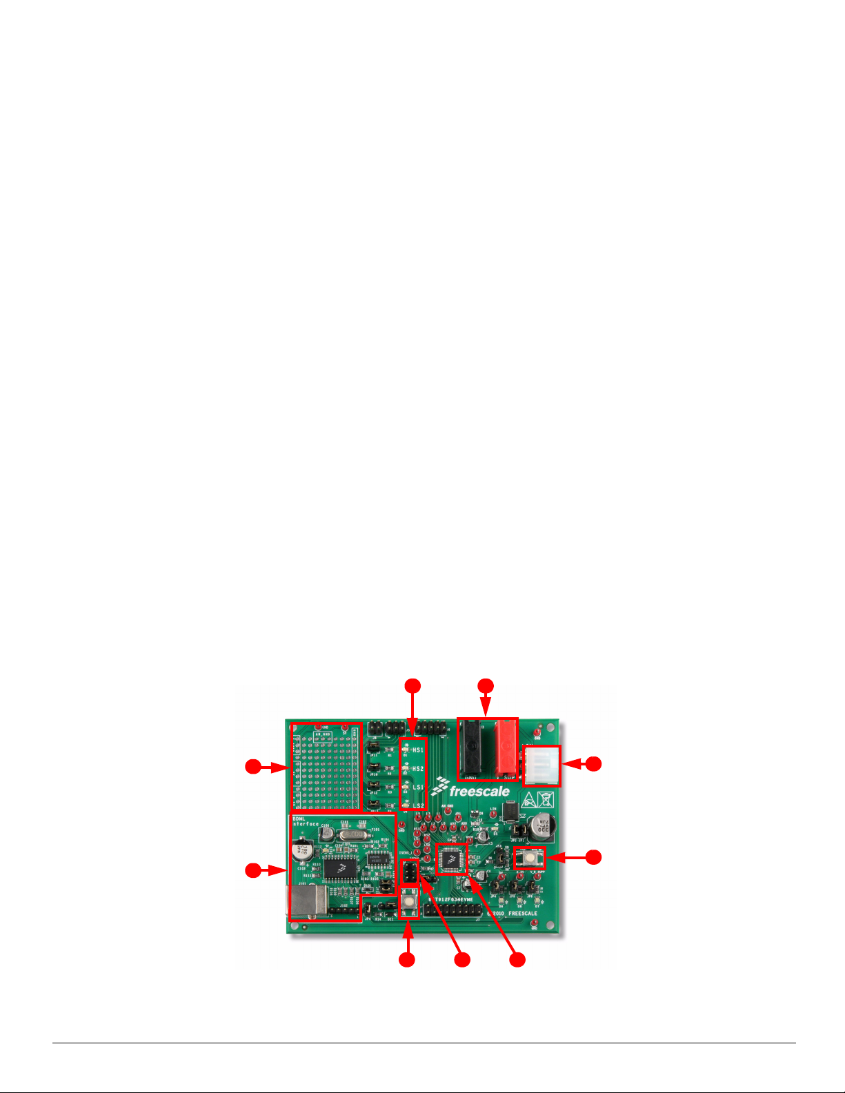
7 Hardware Description
7.1 Board Description
Figure 3 is a snapshot of the EVM with key component and connector locations. The following list corresponds
with the numbers listed on the picture.
1. LEDs to indicate of HS and LS switching
2. Input power connectors
3. Prototype area
4. TBDML interface
5. LIN connector
6. Wake-up button
7. Reset button
8. BDM connector for external programming/debugging BDM interface
9. MM912F634CV1AE
The board is protected against reverse battery voltage by diode D10, which can withstand up to 3.0 A
continuous current. The board operation is straightforward, as is the TDBML interface. (See section “
on page 9), the board contains the passive components required for proper operation of the MM912F634.
Connectors provide access to all device pins and test points for important signals.
TBDML”
There are fifteen jumpers on the board. Power to the LEDs is provided through jumpers JP4, JP8, JP10, JP11,
JP12, and JP13. Removing these jumpers allows low power mode current consumption to be demonstrated.
JP6 supplies power to zener diode D11.
Two push buttons are included: SW1 resets the MCU, and SW2 allows wake-up from one of the low power
modes.
A small prototype area allows fast connection of additional components. Key power and ground vias are located
around the prototype area.
The EVM has three different grounds: LIN ground, main supply ground (also referred to as GND), and analog
ground. All grounds are connected together at a single point on the board, located under the MM912F634. The
bottom copper layer of the EVM and copper areas on the top surface are both assigned to GND.
Figure 3. Evaluation Module Board
KT912F634UG User’s Guide Rev. 2.0 10/2013
8 Freescale Semiconductor, Inc.
Page 9
7.1.1 MCU
JP11
JP1
JP2
JP3
JP4
JP5
JP6
JP7
JP8
JP9
JP12
JP14
JP13
JP15
JP10
The MM912F634 is a single package solution that integrates an HCS12 microcontroller with a SMARTMOS™
analog control IC, interfacing via the new high performance Die-to-Die Interface (D2D). The D2D controlled
analog die combines system basis chip and application specific functions, including a Local Interconnect
Network (LIN) transceiver.
The D2D Interface realizes the advantage of a seamless MCU register map, integrating the analog die registers,
while providing faster access than SPI based systems. The HCS12 includes 32
and a special Die-to-Die Interface, serial peripheral interface (SPI), real time interrupt (RTI), computer operating
properly (COP), and an internal clock generator module. The analog die provides two high side and two low side
outputs with diagnostic functions, voltage regulators for a 5.0
current sense amplifier, four channel timer (TIM), two channel pulse width modulation (PWM) capability, 10
analog to digital converter (ADC), battery voltage sense (VSENSE), and local interconnect network (LIN).
The MM912F634 has three main operating modes: Normal (all functions available); Sleep (VDD off, Wake-up
via LIN, Wake-up inputs (L0-L5), Cyclic Sense, and Forced Wake-up) and Stop (V
capability, Wake-up via LIN bus, Wake-up inputs (L0-L5), Cyclic Sense, forced Wake-up, and external reset).
7.1.2 TBDML
The Turbo BDM Light interface is a programming and debugging tool, and constitutes an interface between a
PC and the BDM debugging port of Freescale microcontrollers. It enables the debugger and other SW tools to
communicate with the microcontroller, and download code into its on-chip flash, etc. Among the benefits of using
the TBDML on the EVM is a much higher communication speed than other USB/BDM interfaces. It is also not
necessary to connect external devices to the EVM when programming/debugging is needed.
A BDM connector (J4) is placed on the EVM to allow the connection of another BDM tool. In this case, the
jumpers JP14 and JP15 should be removed to disable the TBDML interface.
Hardware Description
k of flash memory, 2.0 k of RAM,
V and 2.5 V MCU supply, window watchdog,
on with limited current
DD
bit
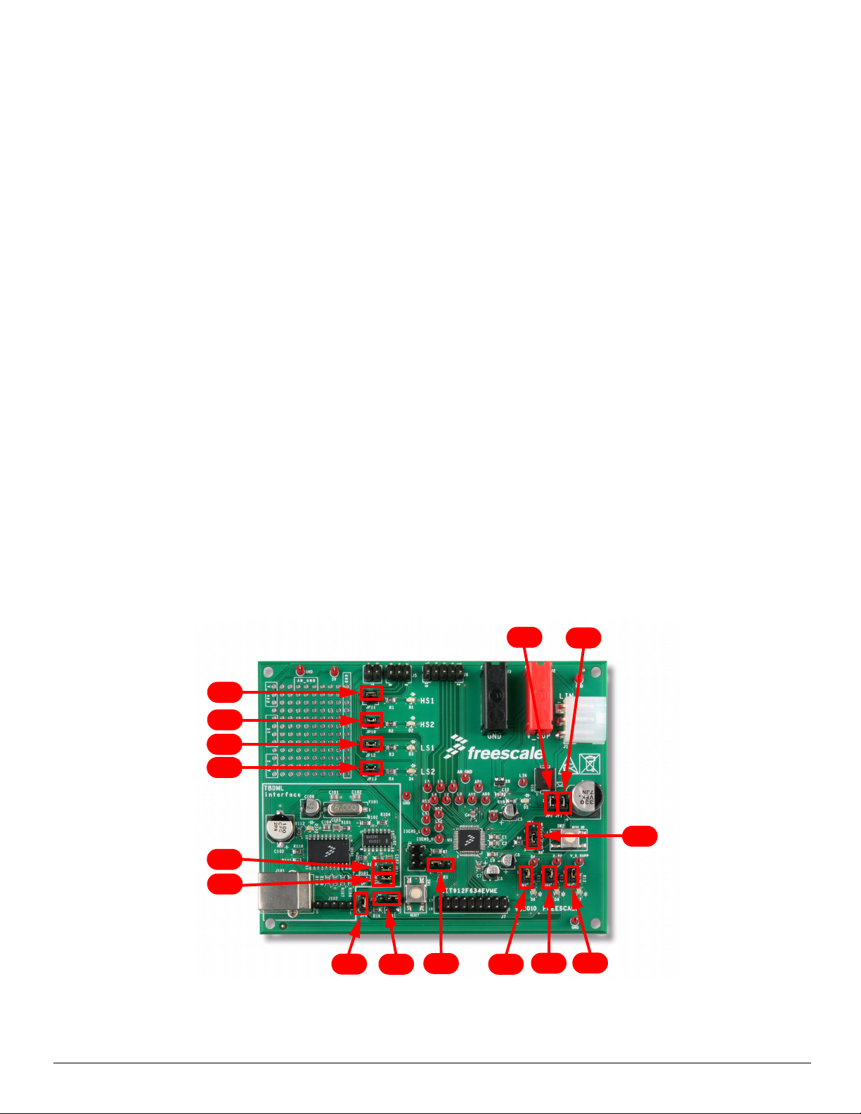
7.2 Jumper Settings
In Figure 4 is the picture of the EVM with location of all jumpers. Table 3 summarizes the jumper settings.
Figure 4. Position of Jumpers on the EVM
KT912F634UG User’s Guide Rev. 2.0 10/2013
Freescale Semiconductor, Inc. 9
Page 10
Hardware Description
Table 3. Jumper Setting
Jumper Function Connections
JP1 Supplying of the device logic (VDDX regulator) and hall sensor supply regulator enabled closed
Supplying of the device logic (VDDX regulator) and hall sensor supply regulator disabled open
JP2 Supplying of the HS drivers enabled closed
Supplying of the HS drivers disabled open
JP3 Wake-up pin L0 connected to HS1 output 1-2
Wake-up pin L0 connected to wake-up button SW2 2-3
JP4 VDDX output voltage (+5.0 V) connected to LED D6 closed
VDDX output voltage (+5.0 V) not connected to LED D6 open
JP5 BKGD/MODC pin connected to +5.0 V via a 3.0 k pull-up resistor 1-2
BKGD/MODC pin connected to GND 2-3
JP6 Supply voltage is connected to Zener diode D11 closed
Supply voltage is not connected to zener diode D11 (when the current consumption of the
device in low power modes is demonstrated).
JP7 TCLK pin (#44) is connected to 8.0 V (also jumper JP6 has to be inserted and the board has
to be powered at least with 8.0 V) to disable of the watchdog.
open
1-2
TCLK pin (#44) is connected to GND 2-3
JP8 Supply voltage (+5.0 to 18 V) is connected to LED D8 closed
Supply voltage (+5.0 to 18 V) is not connected to LED D8 open
JP9 VDD output voltage (+2.5 V) is connected to LED D8 closed
VDD output voltage (+2.5 V) is not connected to LED D8 open
JP10 Diode D2 is connected to output HS2 closed
Diode D2 is not connected to output HS2 open
JP11 Diode D1 is connected to output HS1 closed
Diode D1 is not connected to output HS1 open
JP12 Diode D3 is connected to output LS1 closed
Diode D3 is not connected to output LS1 open
JP13 Diode D4 is connected to output LS2 closed
Diode D4 is not connected to output LS2 open
JP14 BDM signal from TBDML interface enabled closed
BDM signal from TBDML interface disabled, external BDM interface can be used (connected
open
to J4)
JP15 RST signal from TBDML interface enabled closed
RST signal from TBDML interface disabled, external BDM interface can be used (connected
open
to J4)
KT912F634UG User’s Guide Rev. 2.0 10/2013
10 Freescale Semiconductor, Inc.
Page 11
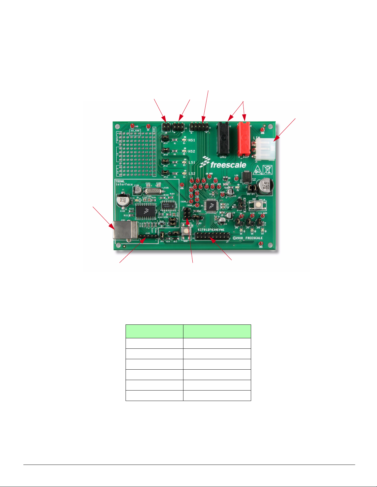
7.3 Connector Description
LIN (J1)
Power (J2 & J3)
BDM (J4)
Signal (J5)
Signal (J6)
Signal (J7)
Signal (J8)
USB (J101)
BDM Programming (J102)
There are 10 connectors on the EVM. A list of the connector and pin assignments are in the following
paragraphs. In the following tables, the “Supply voltage” is meant to supply a voltage protected against a reverse
polarity by diode D10.
Hardware Description
Figure 5. Connectors
7.3.1 Connectors
Tab l e 4. Connector Designations
Connector Location
LIN Connector J1
Power Connector J2 & J3
BDM Connector J4
Signal Connectors J5, J6, J7 &J8
USB Connector J101
BDM J102
KT912F634UG User’s Guide Rev. 2.0 10/2013
Freescale Semiconductor, Inc. 11
Page 12
Hardware Description
7.3.2 LIN Connector J1
The LIN connector allows a connection to the LIN bus, and provides alternate power to the board. It is a MOLEX
multi-pole connector 39-30-3035 (4.20
Tab l e 5. LIN Connector J1
Pin No. Description
1 LIN GND
2 Supply voltage
3 LIN bus
7.3.3 Power Connectors J2, J3
Power connectors J2 (positive supply - red) and J3 (ground - black) are sockets for widely used 4.0 mm banana
jacks.
7.3.4 BDM Connector J4
mm pitch, right angle), and its mating part is MOLEX 39-01-4030.
A standard BDM connector (header 2x3, 2.54 mm (0.1”) pitch) is placed on the EVB, to provide the user an
external BDM programming/debugging interface connection. The pin assignment is listed in
Table 6.
Table 6. BDM Connector
Pin No. Description
1 BKGD
2 GND
3 -
4 /RESET
5 -
6 +5.0 V
KT912F634UG User’s Guide Rev. 2.0 10/2013
12 Freescale Semiconductor, Inc.
Page 13
7.3.5 Signal Connector J5
Connector J5 is the header type 3x2, 2.54 mm (0.1”) pitch. Table 7 shows the pin assignments.
Pin No. Description
7.3.6 Signal Connector J6
The connector type is header 2x5 pins, 2.54 mm pitch. Pin assignment is listed in Table 8.
Hardware Description
Tabl e 7. Signal Connector J5
1 HS1 output
2 HS2 output
3 GND
4 LS1 output
5 LS2 output
6 Supply voltage
Tabl e 8. Signal Connector J6
Pin No. Description
1 HS1 output
2 Wake-up/analog input L0
3 Wake-up/analog input L1
4 Wake-up/analog input L2
5 Wake-up/analog input L3
6 Wake-up/analog input L4
7 Wake-up/analog input L5
8 Supply voltage
9 GND
10 Analog ground
KT912F634UG User’s Guide Rev. 2.0 10/2013
Freescale Semiconductor, Inc. 13
Page 14
Hardware Description
7.3.7 Signal Connector J7
Signal connector J7 contains the ports PTA and PTB, and the output of the Hall sensor supply regulator. Supply
voltage, VDDX regulator output (+5.0
connector J7 has 2 rows of pins, with 0.1” pitch.
Pin No. Description
1 Hall sensor supply regulator output
2 GND
3 PA0
4 PA1
5 PA2
6 PA3
7 PA4
8 PA5
9 PTB1
10 Analog ground
11 PTB2
12 Supply voltage
13 VDDX (+5V)
14 GND
15 PTB0
16 PTB1
17 PTB2
18 Analog ground
V), analog and main supply ground are connected as well. Physically, the
Tabl e 9. Signal Connector J7
7.3.8 Signal Connector J8
The J8 connector is header type 2x2, 0.1” (2.54 mm) pitch.
Pin No. Description
Tab l e 10. Signal Connector J8
1 ISENSE low
2 Analog ground
3 ISENSE high
4 Analog ground
KT912F634UG User’s Guide Rev. 2.0 10/2013
14 Freescale Semiconductor, Inc.
Page 15

7.3.9 USB Connector J101
Connector J101 is a standard USB connector type B. It enables connection of the EVM to a PC or notebook.
Table 11. USB Connector J9
Pin No. Description
1 +5.0 V
2 USBDM
3 USBDP
4 GND
7.3.10 TBDML Programming Connector J102
Connector J102 enables programming of the TBDML firmware in EVM production.
7.4 Test Points
27 test points are on the EVM. The schematic is marked with reference numbers, as well as signal names. The
board is only marked with signal names. The following
Table 12 summarizes the test points.
Hardware Description
Table 12. Test Points
Reference
designator
TP1 HS1 TP14 V
TP2 HS2 TP15 +5.0 V (VDDX out)
TP3 LS1 TP16 LIN
TP4 LS2 TP18 AD0
TP5 ISENSE_H TP19 AD1
TP6 ISENSE_L TP20 AD2
TP7 Hall SUP TP21 2.5 V (VDD out)
TP8 L0 TP22 +5.0 V (VDDX out)
TP9 L1 TP23 GND
TP10 L2 TP24 AN_GND
TP11 L3 TP25 GND
TP12 L4 TP26 GND
TP13 L5 TP27 GND
Signal name
Reference
designator
Signal name
_SUPP
KT912F634UG User’s Guide Rev. 2.0 10/2013
Freescale Semiconductor, Inc. 15
Page 16

Software Description
912F634
EVM Board
TBDML
interface
BDM
J101
USB
PC with
FreeMASTER
software
912F634
EVM Board
TBDML
interface
BDM
J101
USB
PC with
FreeMASTER
software
8 Software Description
8.1 Software Setup
The KIT912F634EVME is designed to communicate with the PC or notebook (as the master) via the USB
interface. The communication is bidirectional. The orders are sent from master, and the status information is
sent from the slave (kit) to the master. The communication methods are described in
this communication, specific software has to be installed on the PC.
Figure 6. In order to enable
Figure 6. Communication Between the PC and the Target
The FreeMASTER software which enables communication with the EVM must be installed on a PC. More
information about this software can be found in the section “
18.
8.1.1 FreeMASTER Software Installation
Before running the application, it is necessary to install the FreeMASTER software included in the jump start
download. See section “
System Requirements - PC Side
• Computer: 486DX/66 MHz or higher processor
• Operating system: Microsoft Windows XP, Windows 2000, WindowsNT4 with SP6, Windows 98
• Required software: Internet Explorer 4.0 or higher. For selected features (e.g. regular expression-based
parsing), Internet Explorer 5.5 or higher is required
• Hard drive space: 8.0 MB
Since the control page requires large data transfer (especially to display the analog values in real time), it is
advisable to use a computer with a more powerful processor.
After executing the following file “FreeMASTER.exe”, the FreeMASTER application will install on the computer.
Follow the instructions for successful installation.
Jump Start” on page 3.
FreeMASTER Graphical User Interface” on page
KT912F634UG User’s Guide Rev. 2.0 10/2013
16 Freescale Semiconductor, Inc.
Page 17

Software Description
8.1.2 FreeMASTER Software Setup
After the application installation, the program is ready for use. To run the program, double click on the
MM912F634_master.pmp file. This file already contains all necessary settings. Ensure that the folder \src is
placed in the same directory as the MM912F634_master.pmp file. The \src folder holds the HTML control
page, java script file and the binary file with the information on the project variables.
NOTE: In order to run FreeMASTER with the MM912F634, the correct firmware must first be compiled and
uploaded in the MM912F634 flash memory. The appropriate Code Warrior project is named
912F634_stationary.mcp and is located in the \EMBSW folder. It is necessary to first install Code Warrior
before this file can be located and opened.
8.2 Important Notes on Programming and Debugging of the Board
8.2.1 Hardware Considerations
There is a software watchdog on the analog die of the device. The watchdog must be cleared by software,
writing certain values into the WDSR register (watchdog service register). Read more about the watchdog in the
MM912F634 data sheet. During device programming, the watchdog must be disabled, otherwise the
programming will not run successfully. To disable the watchdog, a voltage between 7.5 and 10
applied on pin #44 (TCLK). This can be done by inserting a jumper on JP6 and JP7 (1-2). The minimum supply
voltage during the programming and debugging is 8.0
V. A zener diode (D11) on the board provides 8.1 V.
V has to be
8.2.2 Programming and Debugging via the TBDML Interface
A TBDML interface is placed on the kit board for programming/debugging of the board. It is necessary to install
TBDML supporting files (USB driver, interface DLL, and the GDI DLL plug-in for the Freescale’s HI-WAVE
debugger) and implement modifications in the settings of the CodeWarrior HI-WAVE debugger, in order to be
able to program/debug the board. The
and complete source files for this open source tool. Read the user’s manual “tbdml_manual_15.pdf”, especially
the “3.2 Installing Windows Drivers” section, and follow the listed instructions. Omit the jumper J2 settings. It
refers to another board. Installation is easy and does not require any special skills.
Jump Start download (described on page 3) includes the documentation
8.2.3 Programming and Debugging via BDM Interface
Depending on your version of Windows, the TBDML interface may not be compatible. The BDM interface should
be used through the BDM connector’s J4. Open JP14 (BDM signal) and JP15 (RST signal) to use the BDM
interface.
KT912F634UG User’s Guide Rev. 2.0 10/2013
Freescale Semiconductor, Inc. 17
Page 18

Software Description
8.3 FreeMASTER Graphical User Interface
The installation, application setup, and operating instructions were discussed in previous paragraphs. This
section describes the software functionality.
8.3.1 About the FreeMASTER Software
FreeMASTER software (formerly known as PC Master software) is an off board driver supporting
communication between the MM912F634 microcontroller and a PC. This tool allows the programmer to
remotely control an application in a user-friendly graphical environment, running on a PC. It also provides the
ability to view real-time application variables in both text and graphic form. FreeMASTER software is a versatile
tool used for multipurpose algorithms and applications. It provides smart features, including:
• View board application variables - either in the original format, or transformed into a more easily viewable
format
• Modify variable values (in the original or transformed format) to control the board application
• Plot read variable value changes using the Scope feature
• Plot fast events using the Recorder feature
• Control the target application using application commands
• Add HTML pages providing help, or descriptions for the target board application features, scopes and
recorders, application control, etc.
• Create a logical tree structure of blocks relating to the various board application functions, and assign their
corresponding description pages
• Scope and recorder definitions, and watch grids
• Add an HTML based Control page that can control the board application, using standard web tools.
• More about this tool can be found in application note AN2395 (See ”References” section).
8.3.2 FreeMASTER Software on the Embedded Side
8.3.2.1 General Outline
The default communication interface between the PC and the target microcontroller is the SCI (UART). Beside
this, several communication plug-ins were created and added to the FreeMASTER application:
• JTAG/EOnCE (56F8xxx only)
• BDM (HCS08, HCS12 only)
• OSBDML (HC08, HCS12 only), included TBDML
• CAN Calibration Protocol
• Ethernet, TCP/IP
In order to communicate over the SCI, the FreeMASTER software driver must be included in the CodeWarrior
project. It is a set of files that can be downloaded from www.freescale.com for a particular microcontroller family
(8-bit MCU S08, 16-bit MCU S12, 16-bit DSC - MC56F8000, 32-bit ColdFire, 32-bit Power Architecture).
Then in the file freemaster_cfg.h, it is necessary to configure the FreeMASTER serial communication driver.
This is to set the SCI module used (base address of the SCI module used), size of buffer, enable/disable
recorder or scope, mode of operation (interrupt driven or periodic calling), etc.
KT912F634UG User’s Guide Rev. 2.0 10/2013
18 Freescale Semiconductor, Inc.
Page 19

Software Description
8.3.2.2 FreeMASTER with the KIT912F634EVME
Communication between the PC and the embedded application is via the BDM interface. There are several benefits offered by this
solution:
• It is not necessary to add the FreeMASTER source files to the embedded application
• No need to have on-board hardware circuitry for SCI communication over the RS232 interface
• Uses MCU pins dedicated for SCI module to another purpose, or uses the SCI module in the application
(LIN communication).
Of course, there are also some negatives. It is necessary to have BDM multi-link connected all the time to the
board, and the data flow is slower compared to the UART communication. A constraint also occurs during run
or wake-up from low-power modes. Because activity of the BDM affects the core behavior during transition from
reset to normal mode, sometimes the device does not wake-up properly. For this reason, communication is
interrupted by the JavaScript function before the device is put to STOP or SLEEP mode. This feature is
emphasized in other places in this document. See sections dedicated to low power modes.
8.3.3 FreeMASTER Software on the PC
The MM912F634 EVM application uses only two of the FreeMASTER features - reading and writing a value to
the variables on the embedded side. The information on the variable addresses is listed in the binary file
Project.abs stored in the \src directory. It is one of the files generated by CodeWarrior during compilation of the
embedded software project.
8.3.4 Graphical User Interface
Figure 7 is a screen shot of the FreeMASTER PC application, as seen by the user after the opening of the
MM912F634_master.pmp file. It is the start page, where the user can choose an approach to the analog die
registers. The first possibility is “Die Direct Register Access”, and the second is “Analog Die Modules Access”.
Both control pages will be described in the following paragraphs.
Figure 7. FreeMASTER Start Page
KT912F634UG User’s Guide Rev. 2.0 10/2013
Freescale Semiconductor, Inc. 19
Page 20

Software Description
8.3.4.1 Start of the GUI and Troubleshooting (via TBDML)
The MM912F634_master.pmp file contains information regarding communication with the slave, as well as the
information on the variables and the resource files location. By default, the application starts to communicate
with the slave (KIT912F634EVME board) immediately at startup.
• If the slave has no power (USB cable connected, but no supply applied), there is no special error message
displayed. The board will simply not respond to the commands sent from the GUI.
• If the following alert is displayed:
Figure 8. Communication Error Alert
The most likely cause is that the USB cable is not connected, either to the PC or to the KIT908F634EVME board.
Connect the USB cable to the PC and the free end to the KIT board and click “OK”. Then press the “STOP”
button in the FreeMASTER toolbar to restart the communication.
Figure 9. The FreeMASTER Toolbar
If the USB cable is properly connected, the green LED D102 will be blinking.
If the green LED D102 lights permanently, no communication is currently running. To restore communication,
press the “STOP” button in the FreeMASTER toolbar.
KT912F634UG User’s Guide Rev. 2.0 10/2013
20 Freescale Semiconductor, Inc.
Page 21

Software Description
If this action does not help, click in the menu “Project/Options...”, and then in the dialog window select “Comm”
tab. Check if the right communication way is selected:
Figure 10. Options GUI with Comm Tab Displayed
“FreeMASTER OSBDM Communication Plug-in” must be selected. Click the “Configure...” button to check
if the additional settings are correct according to the following dialog window:
Figure 11. Configuring OSBDM Communication
KT912F634UG User’s Guide Rev. 2.0 10/2013
Freescale Semiconductor, Inc. 21
Page 22

Software Description
• There may be an additional issue with the incorrect path to the source files. If the following alert displays,
Click the “OK” button.
The window shown below will appear.
Figure 12. Incorrect Path Error Alert
Figure 13. Missing Symbol Definitions Window
Click the “Continue” button and check the correct path to the source files.
Click on the menu “Project/Options...”, and then in the dialog window, select “MAP Files” tab. The
“P&E_Multilink_CyclonePro.abs” file must be located in the “\src” directory together with the HTML files.
Check the proper selection of the file format (“Binary ELF with DWARF1 or DWARF2 dbg format“).
KT912F634UG User’s Guide Rev. 2.0 10/2013
22 Freescale Semiconductor, Inc.
Page 23

Software Description
Figure 14. Options GUI with MAP Files Tab Displayed
• If the start control page does not look the same as depicted in the Figure 7, but the following information
appears on the screen, then there is a problem with the location of the source files.
Figure 15. Network Error Indicating Problem Locating Source Files
KT912F634UG User’s Guide Rev. 2.0 10/2013
Freescale Semiconductor, Inc. 23
Page 24

Software Description
• To resolve this condition, you will need to perform the following steps: Click on the menu “Project/Options...”,
then in the dialog window select the “HTML Pages” tab. Select the correct path to the “start.html” file. It
should be located in the “\src” directory together with “*.abs” file and the other HTML pages:
“modules.html” and “registers.html”.
Figure 16. Options GUI with HTML Pages Tab Displayed
8.3.4.2 Start of the GUI and Troubleshooting (via BDM)
"click in the menu "Project/Options...", and then in the dialog window select "Comm" tab. Check if the right
communication way is selected:
Figure 17. Options GUI with Comm Tab Displayed
KT912F634UG User’s Guide Rev. 2.0 10/2013
24 Freescale Semiconductor, Inc.
Page 25

Software Description
"FreeMASTER BDM Communication Plug-in" must be selected. Click the "Configure..." button to check if the
additional setting is correct according to following dialog window:
Figure 18. BDM Communication GUI
Click on "Rescan BDM" and next on " Test Connection". A window should appear stating that the BDM cable
is online.
Figure 19. FreeMASTER BDM Plug-in Status Window
KT912F634UG User’s Guide Rev. 2.0 10/2013
Freescale Semiconductor, Inc. 25
Page 26

Software Description
6
10
11
9
5
7
1
2
3
4
8
To restore communication, press the "STOP" button in the FreeMASTER toolbar.
Figure 20. The FreeMASTER Toolbar
8.3.4.3 FreeMASTER Direct Register Access Page
Figure 21 shows the FreeMASTER Direct Register Access control page. The user can read the contents of all
registers, as well as write allowable values to the registers. To enter the value, the user can either click on the
button representing the register bit (with the bit name), or write the number in the edit box in any number format
(dec, hex or bin). There are separate buttons for writing or reading each register. Some registers (mostly related
to the ADC) allow only 16-bit access, therefore there is one big button for reading and writing high and low byte
as single 16-bit value. There are also registers that cannot be modified. In such cases, the button “Write” is
disabled. There are almost 100 registers. The registers are divided into 6 tabs, creating logical groups. On the
right side of the control panel is a field with common functions. The “Read all registers” button is at the top. There
is a group of three radio switches for selection of the number format in which the read values are displayed. The
user can enter the register value in any format, regardless of the format selection. The last function in this field
is a message box to view the entered number information. If the number is not in a supported format, or is
greater than 0xFF, the message “Wrong number” will appear in this message box.
At the top of the control page is a two-line message box showing the BDM protocol error messages.
Figure 21. FreeMASTER Direct Register Access Control Page
KT912F634UG User’s Guide Rev. 2.0 10/2013
26 Freescale Semiconductor, Inc.
Page 27

Table 13. FreeMASTER Direct Register Access Control Page Description
Item Name and Description
1 Six tabs with registers
2 Register address
3 Register name
4 Bit field - by clicking the button the bit value is toggled
5 Numerical value of the register
6 Read and Write buttons
7 BDM communication error
8 “Back” button to return to the start page
9 “Read all Registers” button
10 Selection of number format for all read register values
11 Message box stating whether the correct register value was entered.
Software Description
NOTE: Following a write command to the Mode Control Register, communication between the PC and the target
over the BDM interface will be terminated. See section “
Low Power Modes - STOP Mode and SLEEP Mode”
on page 30for more details.
8.3.4.4 FreeMASTER Analog Die Module Access Page
Figure 22 shows a screen shot of the FreeMASTER control page dedicated to MM912F634 analog die module
access. This control page uses another strategy than previously discussed. The user controls the device by
accessing the properties of the hardware on-chip modules. Each controlled module will be described in more
detail.
Tab l e 14. FreeMASTER Modules Access Control Page Description
Item Name and Description
1 Status field with information about the last reset and wake-up event, as well as
the voltage monitor and watchdog enabler
2 LIN module
3 High side, low side switches and PWM control
4 ADC module
5 Low power modes control
6 BDM communication error
7 “Back” button to return to the start page
KT912F634UG User’s Guide Rev. 2.0 10/2013
Freescale Semiconductor, Inc. 27
Page 28

Software Description
5
3
1
4
6
7
2
Reset status register
Wake-up source register
Voltage status register
Enabling the watchdog
8.3.4.5 Status Block
The status block describes the bit fields of the three status registers - Wake-up source register, Reset status
register, and Voltage status register. Their description is in the MM912F634 data sheet.
The watchdog is enabled after the reset. The user can disable the watchdog, causing the analog die to generate
a core reset. The analog die watchdog can be disabled by applying 8.0
Figure 22. FreeMASTER Modules Access Control Page
Figure 23. Status Block
V to pin TCLK.
KT912F634UG User’s Guide Rev. 2.0 10/2013
28 Freescale Semiconductor, Inc.
Page 29

8.3.4.6 LIN Module
HS/LS switches control
Enabling the PWM channels
Toggling the channels setting
Duty-cycle slider
Frequency slider
Enabling the PWM on the switches
The control panel provides limited LIN functionality. The user can only enable the LIN module and view the
received data. Since the baud rate, message ID, and message size are defined in the LIN slave driver before
the code compilation, these parameters are already preset, and the user is not allowed to modify them.
However, it is possible to change these parameters in the source code and recompile the embedded application.
Figure 24. LIN Module Block
8.3.4.7 High Side and Low Side Switch Control, and PWM Module
The control panel allows full control of the HS and LS switches, in conjunction with the wide frequency range of
the 2-channel PWM module. To turn any switch on, the user must click on one of the four green buttons on the
upper part of the PWM module panel section. The PWM will have no effect on the HS and LS switching unless
the switches are turned on. The PWM channels of the PWM module can be enabled separately by checking the
tick box next to “Enable PWM Channel 0” or “Enable PWM Channel 0”, respectively. The frequency and the duty
cycle are set by a pair of sliders. The PWM module allows setting a positive or negative duty cycle, chosen by
a pair of radio buttons, right of the duty-cycle slider. The value of the PWM frequency is determined by the value
of the frequency slider and the frequency range scroll-down box, positioned right of the frequency slider. The
value of the frequency displayed above the slider is the percentage of the range. There is a pair of radio buttons
named “Channel 0 Setting” and “Channel 1 Setting”. By toggling of these radio buttons, the user can set the
frequency and the duty cycle for both channels. At the bottom of this frame, the user can enable the PWM for
each HS and LS switch independently, as well as assign the PWM channel.
Warning: Even though the PWM module is capable of generating frequencies over 1.0 MHz, the HS and LS
switches can be controlled by frequencies only up to 20
frequencies on the PTB2 output pin.
kHz. The user can test the PWM module at higher
Software Description
Figure 25. HS and LS Switches Control, PWM Module
Freescale Semiconductor, Inc. 29
KT912F634UG User’s Guide Rev. 2.0 10/2013
Page 30

Software Description
Visualization area
Control elements that
allow quantity display
8.3.4.8 ADC Module Control Frame
This frame covers the largest area on the control page, due to the graphical display of sensed analog values in
the graph object. The x-axis represents the time and the y-axis is the numerical representation of the analog
quantity. The y-scale on the left side of the graph area is fixed (0-2500
and AD2 inputs - these are 2.5
displayed quantity (input voltage, chip temperature, current, or value of Lx input). The values of analog inputs
AD0, AD1, and AD2 can be displayed at the same time. The other quantities can only be displayed exclusively.
Analog inputs L0-L5 are displayed exclusively, and the user can switch the range from between 0 to 5.0
0 to 18
V. The history of the sensed quantities is kept in the memory (200 points), so even if the value is currently
not displayed, it is not lost.
There is also a numerical value displayed for battery voltage, temperature, and load current. Since there is not
a fixed value of the current sense resistor placed on the board, the value of the current is listed in raw ADC units,
instead of amps. The amplification of the voltage over the current sense resistor is set to 7 times (this is the
default value after reset). When there is no communication between the PC and the target, the ADC display is
temporarily disabled.
Figure 26 shows the ADC module frame.
V analog inputs. The y-scale on the right side is changed based on the currently
mV). It corresponds to the AD0, AD1,
V and
Figure 26. ADC Module Frame
8.3.4.9 Low Power Modes - STOP Mode and SLEEP Mode
The MM912F634 allows two low power modes. While the device is in the SLEEP mode, the 5.0 V and 2.5 V
regulators are disabled. All values from the registers and variables are cleared, because the device wakes up
from the SLEEP mode transitioning the power-on reset. The STOP mode is the low power mode with higher
current consumption than the SLEEP mode. In STOP mode, the 5.0
limited current capability. The jumpers JP4 and JP9 must be removed, otherwise, a reset will be triggered
(caused by high current consumption of LEDs) and the device will be immediately awakened from the STOP
mode.
There are several options to wake-up the device from the low power modes, supported by the application:
• Forced wake-up - there is a fixed time during which the device is in low power mode
• Wake-up by LIN module
• External reset (reset button SW1) - only from STOP mode
KT912F634UG User’s Guide Rev. 2.0 10/2013
30 Freescale Semiconductor, Inc.
V and 2.5 V regulator are working with
Page 31

Software Description
Action buttons for
entering low power modes
Forced wake-up option
Lx and cyclic sense
wake-up option
click click
• Lx wake-up - the device is awakened when the logical state of any enabled input L0-L5 is detected. The
state of the Lx inputs is checked continuously.
• Cyclic sense wake-up - the same principle as the previous one, but the input Lx is sensed periodically. This
allows lower power consumption during the SLEEP or STOP mode. The Lx inputs are fed by periodic
switching of HS1 or HS2 switch with the corresponding detection of Lx state change.
Figure 27 shows the low power modes frame of the FreeMASTER control page.
Figure 27. Low Power Modes
The low power modes are entered by writing to the Mode Control Register (MCR) of the analog die. Anytime a
write to the MCR register is performed, communication over the BDM interface between the PC and the target
is terminated. The reason is that during wake-up, the device is transitioning from the reset to normal mode. The
BDM interface can interrupt this transition, so the device cannot wake-up properly. After the device completes
the wake-up sequence, the user must restore the BDM communication manually. The user must click twice on
the “Stop” icon, placed on the toolbar of the FreeMASTER application, as shown in
Figure 28. Re-enabling of the BDM Communication After Return from Low Power Modes
8.4 Embedded Software
8.4.1 Main Software Flow Chart
The main embedded software flow chart is shown in Figure 29. After the device and the application initialization,
the software runs in a continuous loop, checking the LIN communication (if enabled) and updating the analog
die registers, based on the FreeMASTER variables and watchdog servicing (if enabled). Other than this, only
one interrupt routine is implemented (D2D_ISR), which handles the SCI receive interrupt routine used by the
LIN slave driver.
Figure 28.
KT912F634UG User’s Guide Rev. 2.0 10/2013
Freescale Semiconductor, Inc. 31
Page 32

Software Description
Reset
LIN
communication
servicing
(LIN enabled) ?
System and
application init
Update analog die
registers based on
the FMaster
variables
(WD enabled) ?
WD servicing
D2D_ISR
LIN_ISR_SCI()
RTI
Clearing the flag
+
+
Infinite loop
Reset
LIN
communication
servicing
(LIN enabled) ?
System and
application init
Update analog die
registers based on
the FMaster
variables
(WD enabled) ?
WD servicing
D2D_ISR
LIN_ISR_SCI()
RTI
Clearing the flag
+
+
Infinite loop
Continuous Loop
Y
Y
N
N
Figure 29. Embedded Software Flow Chart
8.4.2 FreeMASTER Variables
The variables used for the application control have the prefix “fm_”. There is one structure with the name
“fm_register”. The variables of this structure are:
• *fm_address - contains address of the 8-bit register
• fm_data - contains data of the 8-bit register
• *fm_address_16 - contains address of the 16-bit register
• fm_data_16 - contains data of the 16-bit register
• fm_read_write - information on the action - reading or writing to the register
• fm_status - information on the action completion
• fm_size - information on the size of the register (8-bit or 16-bit). The address and data are put in
corresponding variables.
8.4.2.1 Performing the FreeMASTER Variables Update
In the continuous loop, first the value of “fm_status“ is checked. It can have two enumerated values: ”pending”
or “done”. If the value is set to “pending”, then there is a request from the FreeMASTER control panel to read
or write the register value. The value of “fm_read_write“ is then checked to see, if a write or read command is
requested.The value of the variable “fm_size” is evaluated next, to determine if the data is 8 or 16-bit size.
32 Freescale Semiconductor, Inc.
KT912F634UG User’s Guide Rev. 2.0 10/2013
Page 33

The variables “*fm_address“ (pointer to char) or “*fm_address_16“ (pointer to int) have information on the
SciBaudRate
BUSCLK
16 BR⋅
-------------------------
=
register addresses being accessed. If the write command was requested, the values from “fm_data“ or
“fm_data_16“ are written to the address listed in the “*fm_address“ or “*fm_address_16“ variables.
Finally, the variable “fm_status“ is set to “done”. The FreeMASTER then knows that the data was updated.
This code section is also checked if there was a request to enter the STOP mode (if fm_address == 0x216 and
fm_data == 0x1), because first the analog die has to be put in low power mode by writing 0x1 to the Mode
Control Register. The STOP instruction is then executed.
8.4.3 LIN Communication
8.4.3.1 Change of the LIN Communication Parameters
As previously mentioned, LIN communication parameters (baud rate, messages size, messages ID) are set
before code compilation in the LIN software driver. The baud rate can be changed in the file “slave.cfg“. The
baud rate is defined by the following formula:
SciBaudRate is the value written to the SCI baud rate register and BR is the real baud rate value (9600 or
19200). The size of the messages and the ID of the messages can be changed or added in the file “slave.id“.
The ID shall be assigned, based on the LIN 1.3 protocol specification.
Software Description
KT912F634UG User’s Guide Rev. 2.0 10/2013
Freescale Semiconductor, Inc. 33
Page 34

Schematics
5
5
4
4
3
3
2
2
1
1
D D
C C
B B
A A
LIN
LS1
LS2
ISENSE_H
ISENSE_L
L0L1L2L3L4
L5
HSUP
PTB0
PTB1
PTB2
PA0
PA1
PA2
PA3
PA4
PA5
ISENSE_H
LIN
ISENSE_L
HS1
HS1 HS2
PTB0 PTB1
PTB2
LS1
HSUP
LS2
L0
L1 L2
L3
PA1
PA2 PA3
PA4 PA5
L4
L5
PTB0 PTB1
PTB2
PA0
HS1
HS2
TBDM_RST
TBDM
TBDM
TBDM_RST
V_supp
V_D_supp
5V
V_D_supp
V_D_supp
5V
5V
V_D_supp
2p5V
2p5V
5V
2p5V
V_D_supp
V_D_supp
V_D_supp
5V
V_D_supp
5V
2p5V
GND
BDM
BDM_RST
Drawing Title:
Size Document Number Rev
Date: Sheet
of
Page Title:
ICAP Classification: FCP: FIUO: PUBI:
SCH-00355 PDF: SPF-XXXXX 1.2
Quest EVB
A3
Tuesday, January 13, 2009
Quest
12
___ ___
X
Drawing Title:
Size Document Number Rev
Date: Sheet of
Page Title:
ICAP Classification: FCP: FIUO: PUBI:
SCH-00355 PDF: SPF-XXXXX 1.2
Quest EVB
A3
Tuesday, January 13, 2009
Quest
12
___ ___
X
Drawing Title:
Size Document Number Rev
Date: Sheet of
Page Title:
ICAP Classification: FCP: FIUO: PUBI:
SCH-00355 PDF: SPF-XXXXX 1.2
Quest EVB
A3
Tuesday, January 13, 2009
Quest
12
___ ___
X
Off-page
connectors
TP27
GND
TP27
GND
D9
NUP1105LD9NUP1105L
2
1
3
TP14
V_supp
TP14
V_supp
TP20
AD2
TP20
AD2
TP18
AD0
TP18
AD0
J6
CON_2X5J6CON_2X5
1 2
3 4657 8
9 10
SW1 B3S-1000SW1 B3S-1000
1 4
2 3
C9
0.1UFC90.1UF
R12 1KR12 1K
TP9L1TP9
L1
C1
0.1UFC10.1UF
JP13
HDR 1X2
JP13
HDR 1X2
1
2
+
C6
4.7UF+C6
4.7UF
R4 1KR4 1K
TP13L5TP13
L5
D10
MBRS340T3G
D10
MBRS340T3G
2 1
SW2 B3S-1000SW2 B3S-1000
1 4
2 3
JP1
HDR 1X2
JP1
HDR 1X2
1
2
R10 1KR10 1K
JP10
HDR 1X2
JP10
HDR 1X2
1
2
C10
68pF
C10
68pF
D6
GreenD6Green
2 1
JP6
HDR 1X2
JP6
HDR 1X2
1
2
J3
BANANA BLACK
J3
BANANA BLACK
1
2
JP3
HDR_1X3
JP3
HDR_1X3
123
R14 820R14 820
J7
HDR 2X9J7HDR 2X9
1 2
3 4657 8
9 10
11 12
13 14
15 16
17 18
SH3SH3
JP7
HDR_1X3
JP7
HDR_1X3
123
TP26
GND
TP26
GND
C7
0.1UFC70.1UF
R5 3.3KR5 3.3K
TP3
LS1
TP3
LS1
D5
LGR971D5LGR971
2 1
JP9
HDR 1X2
JP9
HDR 1X2
1
2
TP12L4TP12
L4
R13 100R13 100
TP5
ISENSE_H
TP5
ISENSE_H
D1
GreenD1Green
2 1
D7
GreenD7Green
2 1
TP19
AD1
TP19
AD1
TP8L0TP8
L0
JP11
HDR 1X2
JP11
HDR 1X2
1
2
C4
0.1UFC40.1UF
C2
0.1UFC20.1UF
TP155VTP15
5V
JP15
HDR 1X2
JP15
HDR 1X2
1
2
TP23
GND
TP23
GND
D4
YellowD4Yellow
21
R3 1KR3 1K
U2
prototype areaU2prototype area
11223344556677889
9
1010111112
12
85
85
86
86
87
87
88
88
89
89
90
90
91
91
92
92
93
93
94
94
95
95
96
96
13
13
14
14
15
15
16
16
17
17
18
18
19
19
20
20
21
21
22
22
23
23
24
24
25
25
26
26
27
27
28
28
29
29
30
30
31
31
32
32
33
33
34
34
35
35
36
36
37
37
38
38
39
39
40
40
41
41
42
42
43
43
44
44
45
45
46
46
47
47
48
48
49
49
50
50
51
51
52
52
53
53
54
54
55
55
56
56
57
57
58
58
59
59
60
60
61
61
62
62
63
63
64
64
65
65
66
66
67
67
68
68
69
69
70
70
71
71
72
72
73
73
74
74
75
75
76
76
77
77
78
78
79
79
80
80
81
81
82
82
83
83
84
84
97
97
98
98
99
99
100
100
101
101
102
102
103
103
104
104
105
105
106
106
107
107
108
108
109
109
110
110
111
111
112
112
113
113
114
114
115
115
116
116
117
117
118
118
119
119
120
120
TP24
AN_GND
TP24
AN_GND
TP21
2p5V
TP21
2p5V
D8
GreenD8Green
2 1
TP11L3TP11
L3
J8
HDR 2X2J8HDR 2X2
1 2
3 4
TP25
GND
TP25
GND
J5
HDR 2X3J5HDR 2X3
1 2
3 4
65
JP5
HDR_1X3
JP5
HDR_1X3
123
R2 1KR2 1K
J2
BANANA REDJ2BANANA RED
1
2
R8 33KR8 33K
R7 3.3KR7 3.3K
R91KR9
1K
TP2
HS2
TP2
HS2
J1
39-30-3035J139-30-3035
123
TP4
LS2
TP4
LS2
D11
MMSZ8V2T1G
D11
MMSZ8V2T1G
2 1
R11 200RR11 200R
TP225VTP22
5V
TP1
HS1
TP1
HS1
R6 10KR6 10K
D2
GreenD2Green
2 1
JP2
HDR 1X2
JP2
HDR 1X2
1
2
R1 1KR1 1K
TP10L2TP10
L2
TP6
ISENSE_L
TP6
ISENSE_L
+
C3
330UF+C3
330UF
JP8
HDR 1X2
JP8
HDR 1X2
1
2
+
C5
10UF+C5
10UF
SH2SH2
J4
HDR 2X3J4HDR 2X3
1 2
3 4
65
JP12
HDR 1X2
JP12
HDR 1X2
1
2
+
C8
4.7UF+C8
4.7UF
TP16
LIN
TP16
LIN
D3
YellowD3Yellow
21
JP4
HDR 1X2
JP4
HDR 1X2
1
2
U1
MM912F634AVAM
U1
MM912F634AVAM
PA5
5
L0
31
XTAL3EXTAL
2
RESET_A45TEST
4
RESET
46
VS2
20
PGND
38
LS1
37
VSENSE
18
VS1
19
HS2
22
L334L2
33
VDD
15
L1
32
PA1/MOSI9PA0/MISO
10
HS1
21
EVDD
14
PA2/SCK
8
TCK44PA3/SS7PA4
6
L435L5
36
ISENSEH
41
LS2
39
PTB0/AD0/RX/TIM0CH0
26
PTB1/AD1/TX/TIM0CH1
27
PTB2/AD2/PWM/TIM0CH2
28
BKGD/MODC
47
LIN
24
ISENSEL
40
LGND
25
TEST_A
43
AGND
30
HSUP
23
EPAD
49
ADC2p529VDDX16EVSS13EVSSX
11
EVDDX12DGND
17
NC1NC248NC(VFUSE)
42
JP14
HDR 1X2
JP14
HDR 1X2
1
2
TP7
HSUP
TP7
HSUP
9 Schematics
34 Freescale Semiconductor, Inc.
Figure 30. Evaluation Board Schematic, Part 1
KT912F634UG User’s Guide Rev. 2.0 10/2013
Page 35

Schematics
5
5
4
4
3
3
2
2
1
1
D D
C C
B B
A A
BDM_OUT
BDM_DRV RST_OUT
BDM
RST_OUT
BDM_DRV
RST_IN
BDM_IN
BDM_OUT
IRQ
BDM_DRV
USBDM
USBDP
BDM_IN MONITOR
BDM_RST
BDM_IN RST_IN
USBDM
USBDP
MONITOR
BDM_RST
BDM
IRQ
+3.3V
+3.3V +3.3V
+3.3V
+5V
+5V
+5V
+5V
+5V +3.3V +5V
+5V
+5V
GND
BDM
BDM_RST
Drawing Title:
Size Document Number Rev
Date: Sheet
of
Page Title:
ICAP Classification: FCP: FIUO: PUBI:
SCH-XXXXX PDF: SPF-XXXXX 1.2
Quest EVB
A3
Tuesday, January 13, 2009
TBDML interface
22
___ ___
X
Drawing Title:
Size Document Number Rev
Date: Sheet of
Page Title:
ICAP Classification: FCP: FIUO: PUBI:
SCH-XXXXX PDF: SPF-XXXXX 1.2
Quest EVB
A3
Tuesday, January 13, 2009
TBDML interface
22
___ ___
X
Drawing Title:
Size Document Number Rev
Date: Sheet of
Page Title:
ICAP Classification: FCP: FIUO: PUBI:
SCH-XXXXX PDF: SPF-XXXXX 1.2
Quest EVB
A3
Tuesday, January 13, 2009
TBDML interface
22
___ ___
X
BDM DRIVER
USB INTERFACE
R1OUT
T1IN
For programming
of the HC908 device.
Connect to the
external MAX3232.
908JB8 HC125
+10V for IRQ high voltage during programming
GND
+5V for supply of standalone MAX3232
Off-page
connectors
U102D
MC74HC125ADG
U102D
MC74HC125ADG
12 11
13
U101
MC908JB8JDWE
<ICA_MFR_NAME>
U101
MC908JB8JDWE
<ICA_MFR_NAME>
PTE3/D+8PTE1/TCH0
7
PTA7/KBA7
12
PTA6/KBA6
13
PTA5/KBA5
14
PTA4/KBA415PTA3/KBA3
16
PTA2/KBA2
17
PTA1/KBA1
18
PTA0/KBA0
19
RESET
20
IRQ
11
VREG4PTD0/1
6
VDD
5
VSS
1
PTE4/D-
9
OSC23OSC1
2
PTC0
10
R107
10K
R107
10K
D102
HSMY-C170
D102
HSMY-C170
2 1
+
C103
100UF+C103
100UF
C105
0.1uF
C105
0.1uF
J102
HDR_1X5
J102
HDR_1X5
12345
R101
10M
R101
10M
U102B
MC74HC125ADG
U102B
MC74HC125ADG
56
4
1
2
34
+D
-DGV
J101
USB_TYPE_B
1
2
34
+D
-DGV
J101
USB_TYPE_B
1234S1
S2
R106
10K
R106
10K
R10447R104
47
C101
22PF
C101
22PF
R103
1.8K
R103
1.8K
R110 27R110 27
R109
10K
R109
10K
+
C106
100UF+C106
100UF
C107
0.1uF
C107
0.1uF
R111 27R111 27
R112
330
R112
330
VCC
GND
U102A
MC74HC125ADG
VCC
GND
U102A
MC74HC125ADG
2 3
1417
C102
22PF
C102
22PF
U102C
MC74HC125ADG
U102C
MC74HC125ADG
98
10
D101
1N4148WS
D101
1N4148WS
2 1
R10547R105
47
Y101
6.0MHz
Y101
6.0MHz
1 2
C104
0.1uF
C104
0.1uF
R108
10K
R108
10K
R102
1.8K
R102
1.8K
Freescale Semiconductor, Inc. 35
Figure 31. Evaluation Board Schematic, Part 2
KT912F634UG User’s Guide Rev. 2.0 10/2013
Page 36

Board Layout
10 Board Layout
10.1 Assembly Layer Top
KT912F634UG User’s Guide Rev. 2.0 10/2013
36 Freescale Semiconductor, Inc.
Page 37

10.2 Assembly Layer Bottom
Note: This image is an exception to the standard top-view mode of representation used in this document. It has been flipped to show a
bottom view.
Board Layout
KT912F634UG User’s Guide Rev. 2.0 10/2013
Freescale Semiconductor, Inc. 37
Page 38

Board Layout
10.3 Top Layer Routing
KT912F634UG User’s Guide Rev. 2.0 10/2013
38 Freescale Semiconductor, Inc.
Page 39

10.4 Bottom Layer Routing
Board Layout
KT912F634UG User’s Guide Rev. 2.0 10/2013
Freescale Semiconductor, Inc. 39
Page 40

Bill of Materials
11 Bill of Materials
Qty. Schematic Label Value Description Mfg. Mfg. Part No.
8 C1, C2, C4, C7, C9,
C104, C105, C107
1 C3 330 μF/35 V Electrolytic Capacitor
1 C5 10 μF/16 V Electrolytic Capacitor
2 C6, C8 47 μF/50 V Electrolytic Capacitor
1 C10 68 pF/50 V Ceramic capacitor, 0805,
2 C101, C102 22 pF/100 V Ceramic capacitor, 0805,
1 C106 100 μF/6.3 V Electrolytic capacitor,
1 C103 100 μF/20 V Electrolytic capacitor,
7 D1, D2, D5, D6, D7, D8,
D102
2 D3, D4 LED, yellow, SMD 0805 KINGBRIGHT KP-2012SYC
1 D9 Single Line CAN/LIN Bus
1 D10 3.0 A, 40 V Schottky
100 nF/50 V Ceramic capacitor, 0805,
100 nF/50 V
SMD, 330
SMD, 10
SMD, 47 μF/25 V
68 pF/50 V
22
SMD, 100 μF/6.3 V
SMD, 100 μF/20 V
LED, green, SMD 0805 KINGBRIGHT KP-2012MGC
Protector
Rectifier
μF/35 V
μF/16 V
pF/100 V
Kemet 08055C104KAT2A
Panasonic EEEFK1V331AP
Panasonic EEE1CA100SR
Panasonic EEE1EA4R7SR
Kemet C1206C475K3PAC
Kemet C0805C220J1GAC
Panasonic EEEFKJ101UAR
Nichicon PCF1D101MCL1GS
On Semi NUP1105L
On Semi MBRS340T3G
1 D11 Zener Diode 500 mW,
8.2 V
1 D101 DIODE, HIGH SPEED,
V, 15 0 mA
100
12 JP1, JP2, JP4, JP6, JP8,
JP9, JP10, JP11, JP12,
JP13, JP14, JP15
3 JP3, JP5, JP7 Header 2.54 mm, 3x1 Molex 90120-0763
1 J1 Connector 1x3, 4.20 mm
1 J2 Banana socket, 4.0 mm,
1 J3 Banana socket, 4.0 mm,
1 J4,J5 Header 2.54 mm, 3x2 Molex 90131-0763
1 J6 Header 2.54 mm, 5x2 Molex 90131-0765
1 J7 Header 2.54 mm, 9x2 Molex 90131-0769
1 J8 Header 2.54 mm, 2x2 Molex 90131-0762
Header 2.54 mm, 2x1 Molex 90120-0762
pitch, shrouded, right
angle
PCB, RED
BLACK
On Semi MMSZ8V2T1G
MULTICOMP 1N4148WS
Molex 39-30-3035
Hirschman PB4RED
Hirschman PB4BLACK
KT912F634UG User’s Guide Rev. 2.0 10/2013
40 Freescale Semiconductor, Inc.
Page 41

Bill of Materials
Qty. Schematic Label Value Description Mfg. Mfg. Part No.
1 J101 USB TYP B WRCOM 4
PINS
WUERTH
ELEKTRONIK
61400416121
1 J102 Header 2.54 mm, 1x5 Molex 90120-0765
7 R1, R2, R3, R4, R9, R10,
1.0 k Resistor 1.0 kΩ, 5%, 0805 Multicomp MC 0.1W 0805 5% 1K
R12
2 R5, R7 3.3 k Resistor 3.3 kΩ, 5%, 0805 Multicomp MC 0.1W 0805 5%
3K3
5 R6,R106, R107, R108,
R109
10 k Resistor 10 kΩ, 5%, 0805 Multicomp MC 0.1W 0805 5%
10K
1 R8 33 k Resistor 33 kΩ, 5%, 0805 Multicomp MC 0.1W 0805 5%
33K
1 R11 200 Resistor 200Ω, 5%, 0805 Multicomp MC 0.1W 0805 5%
200R
1 R13 100 Resistor 100Ω, 5%, 0805 Multicomp MC 0.1W 0805 5%
100R
1 R14 820 Resistor 820Ω, 5%, 0805 Multicomp MC 0.1W 0805 5%
820R
1 R101 10 M Resistor 10 MΩ, 5%, 0805 PHYCOMP
232273061106
(YAGEO)
2 R102, R103 1.8 K Resistor 1.8 kΩ, 5%, 0805 Multicomp MC 0.1W 0805 5%
1K8
2 R104, R1054 47 Resistor 47 Ω, 5%, 0805 Multicomp MC 0.1W 0805 5%
47R
2 R110, R111 27 Resistor 27 Ω, 5%, 0805 Multicomp MC 0.1W 0805 5%
27R
1 R112 330 Resistor 300 Ω, 5%, 0805 Multicomp MC 0.1W 0805 5%
300R
2 SW1, SW2 Switch SMD OMRON
B3S-1000
ELECTRONIC
COMPONENTS
1 U1 Integrated S12 MagniV
Based Relay Driver with
Freescale
Semiconductor
MM912F634CV1AE
LIN
1 U101 8-bit microcontroller Freescale
MC908JB8JDWE
Semiconductor
1 U102 Quad Noninverting Buffer,
On Semi MC74HC125ADG
3 State
1 Y101 6.0 MHz Crystal, 6.0 MHz, SMD Vishay Dale XT49M-206M
KT912F634UG User’s Guide Rev. 2.0 10/2013
Freescale Semiconductor, Inc. 41
Page 42

Bill of Materials
Qty. Schematic Label Value Description Mfg. Mfg. Part No.
26 TP1, TP2, TP3, TP4,
TP5, TP6, TP7, TP8,
TP9, TP10, TP11, TP12,
TP13, TP14, TP15,
TP16, TP18, TP19,
TP20, TP21, TP22,
TP23, TP24, TP25,
TP26. TP27
HS1, HS2, LS1,
LS2, ISENSE_H,
ISENSE_L,
HSUP, L0, L1, L2,
L3, L4, L5,
V_D_supp, 5V,
LIN, AD0, AD1,
AD2, 2.5V, 5V,
Test points Keystone 5002
GND, AN_GND,
GND, GND, GND
Note: Freescale does not assume liability, endorse, or warrant components from external manufacturers that are referenced in circuit
drawings or tables. While Freescale offers component recommendations in this configuration, it is the customer’s responsibility to validate
their application.
KT912F634UG User’s Guide Rev. 2.0 10/2013
42 Freescale Semiconductor, Inc.
Page 43

12 References
Following are URLs where you can obtain information on other Freescale products and application solutions:
References
Document Number
and Description
AN2395 Application
Note
http://cache.freescale.com/files/microcontrollers/doc/app_note/AN2395.pdf?fsrch=1&sr=1
Freescale.com
Support Pages
KIT912F634EVME
Tool Summary Page
MM912_634
Product Summary Page
FreeMASTER Run-Time
Debugger
Tool Summary Page
Analog Home Page http://www.freescale.com/analog
Power Management
Home Page
http://preview.freescale.net/webapp/sps/site/prod_summary.jsp?code=KIT912F634EVME
http://www.freescale.com/webapp/sps/site/prod_summary.jsp?code=MM912_634
http://www.freescale.com/webapp/sps/site/prod_summary.jsp?code=FREEMASTER
www.freescale.com/powermanagement
12.1 Support
Visit www.freescale.com/support for a list of phone numbers within your region.
URL
URL
12.2 Warranty
Visit www.freescale.com/warranty for a list of phone numbers within your region.
KT912F634UG User’s Guide Rev. 2.0 10/2013
Freescale Semiconductor, Inc. 43
Page 44

Revision History
13 Revision History
Revision Date Description of Changes
1.0 11/2010 Initial Release
2.0 10/2013 Added new chapter: “Start of the GUI and Troubleshooting (via BDM)”
KT912F634UG User’s Guide Rev. 2.0 10/2013
44 Freescale Semiconductor, Inc.
Page 45

Revision History
KT912F634UG User’s Guide Rev. 2.0 10/2013
45 Freescale Semiconductor, Inc.
Page 46

How to Reach Us:
Home Page:
freescale.com
Web Support:
freescale.com/support
Information in this document is provided solely to enable system and software implementers to use Freescale
products. There are no express or implied copyright licenses granted hereunder to design or fabricate any integrated
circuits based on the information in this document.
Freescale reserves the right to make changes without further notice to any products herein. Freescale makes no
warranty, representation, or guarantee regarding the suitability of its products for any particular purpose, nor does
Freescale assume any liability arising out of the application or use of any product or circuit, and specifically disclaims
any and all liability, including without limitation consequential or incidental damages. “Typical” parameters that may be
provided in Freescale data sheets and/or specifications can and do vary in different applications, and actual
performance may vary over time. All operating parameters, including “typicals,” must be validated for each customer
application by customer’s technical experts. Freescale does not convey any license under its patent rights nor the
rights of others. Freescale sells products pursuant to standard terms and conditions of sale, which can be found at the
following address: freescale.com/SalesTermsandConditions.
Freescale and the Freescale logo are trademarks of Freescale Semiconductor, Inc., Reg. U.S. Pat. & Tm. Off. MagniV
(912_634) and SMARTMOS are trademarks of Freescale Semiconductor, Inc. All other product or service names are
the property of their respective owners.
© 2013 Freescale Semiconductor, Inc.
Document Number: KT912F634UG
Rev. 2.0
10/2013
 Loading...