

Page 1
Freescale Semiconductor
Document Number: KT33932UG
User’s Guide
KIT33932VWEVBE Evaluation Board
Rev. 2.0, 4/2011
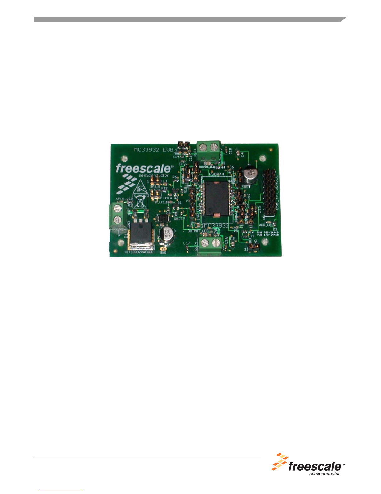
Figure 1. Evaluation Board
Table of Contents
Kit Contents / Packing List . . . . . . . . . . . . . . . . . . . . . . . . . . . . . . . . . . . . . . . . . . . . . . . . . . . . . . . . . . . . . . . . . . . . . . . 2
Important Notice. . . . . . . . . . . . . . . . . . . . . . . . . . . . . . . . . . . . . . . . . . . . . . . . . . . . . . . . . . . . . . . . . . . . . . . . . . . . . . . 3
Kit Introduction . . . . . . . . . . . . . . . . . . . . . . . . . . . . . . . . . . . . . . . . . . . . . . . . . . . . . . . . . . . . . . . . . . . . . . . . . . . . . . . 4
Hardware Description. . . . . . . . . . . . . . . . . . . . . . . . . . . . . . . . . . . . . . . . . . . . . . . . . . . . . . . . . . . . . . . . . . . . . . . . . . 5
Setup and Example Demonstrations . . . . . . . . . . . . . . . . . . . . . . . . . . . . . . . . . . . . . . . . . . . . . . . . . . . . . . . . . . . . . . . 8
EVB Schematic. . . . . . . . . . . . . . . . . . . . . . . . . . . . . . . . . . . . . . . . . . . . . . . . . . . . . . . . . . . . . . . . . . . . . . . . . . . . . . . 9
Board Layout . . . . . . . . . . . . . . . . . . . . . . . . . . . . . . . . . . . . . . . . . . . . . . . . . . . . . . . . . . . . . . . . . . . . . . . . . . . . . . . . 10
Bill of Material. . . . . . . . . . . . . . . . . . . . . . . . . . . . . . . . . . . . . . . . . . . . . . . . . . . . . . . . . . . . . . . . . . . . . . . . . . . . . . . . 12
References . . . . . . . . . . . . . . . . . . . . . . . . . . . . . . . . . . . . . . . . . . . . . . . . . . . . . . . . . . . . . . . . . . . . . . . . . . . . . . . . . 14
Revision History . . . . . . . . . . . . . . . . . . . . . . . . . . . . . . . . . . . . . . . . . . . . . . . . . . . . . . . . . . . . . . . . . . . . . . . . . . . . . 15
© Freescale Semiconductor, Inc., 2009 - 2011. All rights reserved.
Page 2

1 Kit Contents / Packing List
• Evaluation Board - KIT33932VWEVBE
• Hardware Document CD, CD33932
• Warranty Card, Freescale, 920-75133, Rev. A
• Technical Information Center Freescale Semiconductor, Inc. BR1530
• FCC Disclaimer, Freescale, 926-75760, Rev A
Kit Contents / Packing List
Freescale Semiconductor 2
KIT33932VWEVBE Evaluation Board, Rev. 2.0
Page 3

2 Important Notice
Freescale provides the enclosed product(s) under the following conditions:
This evaluation kit is intended for use of ENGINEERING DEVELOPMENT OR EVALUATION PURPOSES ONLY. It is
provided as a sample IC pre-soldered to a printed circuit board to make it easier to access inputs, outputs, and supply
terminals. This EVB may be used with any development system or other source of I/O signals by simply connecting it
to the host MCU or computer board via off-the-shelf cables. This EVB is not a Reference Design and is not intended to
represent a final design recommendation for any particular application. Final device in an application will be heavily
dependent on proper printed circuit board layout and heat sinking design as well as attention to supply filtering, transient
suppression, and I/O signal quality.
The goods provided may not be complete in terms of required design, marketing, and or manufacturi ng related
protective considerations, including product safety measures typically found in the end product incorporating the goods.
Due to the open construction of the product, it is the user's responsibility to take any and all appropriate precautions with
regard to electrostatic discharge. In order to minimize risks associated with the customers applications, adequate design
and operating safeguards must be provided by the customer to minimize inherent or procedural hazards. For any safety
concerns, contact Freescale sales and technical support services.
Should this evaluation kit not meet the specifications indicated in the kit, it may be returned within 30 days from the date
of delivery and will be replaced by a new kit.
Freescale reserves the right to make changes without further notice to any products herein. Freescale makes no
warranty, representation or guarantee regarding the suitability of its products for any particular purpose, nor does
Freescale assume any liability arising out of the application or use of any product or circuit, and specifically disclaims
any and all liability, including without limitation consequential or incidental damages. “Typical” parameters can and do
vary in different applications and actual performance may vary over time. All operating parameters, including “Typical”,
must be validated for each customer application by customer’s technical experts.
Freescale does not convey any license under its patent rights nor the rights of others. Freescale products are not
designed, intended, or authorized for use as components in systems intended for surgical implant into the body , or other
applications intended to support or sustain life, or for any other application in which the failure of the Freescale product
could create a situation where personal injury or death may occur.
Should Buyer purchase or use Freescale products for any such unintended or unauthorized application, Buyer shall
indemnify and hold Freescale and its officers, employees, subsidiaries, affiliates, and distributors harmless against all
claims, costs, damages, and expenses, and reasonable attorney fees arising out of, directly or indirectly, any claim of
personal injury or death associated with such unintended or unauthorized use, even if such claim alleges that Freescale
was negligent regarding the design or manufacture of the part.Freescale™ and the Freescale logo are trademarks of
Freescale Semiconductor, Inc. All other product or service names are the property of their respective owners. ©
Freescale Semiconductor, Inc. 2008
Important Notice
Freescale Semiconductor 3
KIT33932VWEVBE Evaluation Board, Rev. 2.0
Page 4

Kit Introduction
3 Kit Introduction
• The KIT33932VWEVBE Evaluation Board (EVB) is an easy-to-use circuit board that
allows the user to exercise all the functions of the MC33932 H-Bridge circuit. The EVB
parallel input can be easily controlled through a USB/SPI Dongle connected to a PC’s
USB port. The Freescale SPIGen program provides the User Interface to the USB/SPI
Dongle and allows the user to send commands to the IC.
Freescale Semiconductor 4
KIT33932VWEVBE Evaluation Board, Rev. 2.0
Page 5
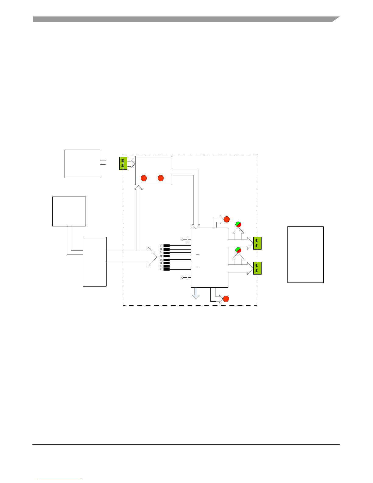
4 Hardware Description
Reverse Battery
And Transient
Protection
MC 33932
Dual
H-Bridge
MC33932 Evaluation Board Block Diagram
16 conductor Flat Cable
VPWR
LED
VBat
2
VPWR,
VDD
USB/SPI
DONGLE
VDD
LED
H-BRIDGE
OUT1, OUT2
Screw
Connectors
VDD
INPUT 1
INPUT 2
D1
EN/D2
INPUT 3
INPUT 4
D3
EN/D4
FAULT
LED
JUMPERS
2
2
H-BRIDGE
OUT3, OUT4
Screw
Connectors
FAULT
LED
OUTPUT
POLARITY
LEDS
DATA0
DATA1
DATA2
DATA3
CNTL0
CNTL2
CNTL3
CNTL1
All Grounds
VPWR
VPWR
Charge
Pump
Cap
Charge
Pump
Cap
LOADS
KIT33932VMEVBE
KITUSBSPIDGLEVME
PC
USB
Cable
Power
Supply
4.1 Recommended Equipment
• PC Computer running Windows XP
• 5-40V Power Supply
• USB Cable
• KITUSBSPIDGLEVME
The Hardware Block Diagram is shown below:
Hardware Description
This EVB consists of a Dual H-Bridge, a parallel interface, power conditioning circuitry, and a set of 8 Input Select Jumpers.
All +5 volt VDD power required by the EVB is obtained via the parallel interface.
4.2 LED Display
Several LED’s are provided as visual output devices for the EVB. A list of the LED devices is shown below:
1. VDD LED - Indicates when +5 Volt supply is connected
2. VPWR LED - Indicates when +12 Volt supply is connected
3. Fault LEDs - Illuminates when one of the H-Bridges detects a fault
4. Output LEDs - Red/Green LED, for each H-Bridge, that indicates which direction the current is flowing in the legs of the
H-Bridge.
Freescale Semiconductor 5
Figure 2. Block Diagram
KIT33932VWEVBE Evaluation Board, Rev. 2.0
Page 6

Hardware Description
4.3 I/O Jumper Definitions (J3)
The EVB contains seven jumpers that connect the inputs of the 33932 as follows (Bold = factory setting):
JUMPER NAME JUMPER POSITION CONNECTION
INPUT 1 1-2/2-3 GND/DATA0
INPUT 2 1-2/2-3 GND/DATA1
INPUT3 1-2/2-3 GND/DATA2
INPUT4 1-2/2-3 GND/DATA3
ENABLE/DISABLE 2 1-2/2-3 PullUp/CNTL1
ENABLE/DISABLE 4 1-2/2-3 PullUp/CNTL3
DISABLE 1 1-2/2-3 CNTL0/GND
DISABLE_2B 1-2/2-3 GND/CNTL2
The DATA0 -DATA3 and CNTL0 - CNTL3 signals are parallel outputs from the USB/SPI Dongle that can be controlled directly
from the SPIGen program. An example config file called “MC33932_EVB_CONFIGURATION_FILE.spi” is provided on the
CD which contains a batch file example.
If the user prefers to supply the various MC33932 input signals externally, other than from the USB-SPI Interface, the jumpers
can be removed and connections can be made to the open pin number 2’ s.
4.4 USB/SPI Dongle Connector
The USB/SPI dongle connector is a 16 pin,.1” center, dual-row connector that is designed to interface directly to the USB/SPI
Dongle unit. The USB/SPI dongle connector consists of the following 16 pins –
Pin Number Name Description
1 CSB SPI signal, Chip Select Bar
2 CNTL2 Parallel po rt signal CNTL2
3 SO SPI signal, Serial Out
4 CNTL1 Parallel po rt signal CNTL1
5 SI SPI signal, Serial In
6 CNTL0 Parallel po rt signal CNTL0
7 SCLK SPI signal, Serial Clock
8 DATA4 Parallel port signal DATA4
9 CNTL3 Parallel po rt signal CNTL3
10 DATA3 Parallel port signal DATA3
11 VDD +5 Volt VDD from USB
12 DATA2 Parallel port signal DATA2
13 NC Unused
14 DATA1 Parallel port signal DATA1
15 GND Signal Ground
16 DATA0 Parallel port signal DATA0
This connector mates with the 16 conductor flat cable that connects to the USB/SPI Dongle (KITUSBSPIDGLEVME).
Freescale Semiconductor 6
KIT33932VWEVBE Evaluation Board, Rev. 2.0
Page 7

Hardware Description
VBAT
CONNECTOR
OUTPUT
1 &2
CONNECTOR
OUTPUT 3 & 4
CONNECTOR
PARALLEL
CONNECTOR
4.5 Screw Terminal Connections
The EVB contains input and output screw terminal connections to allow easy access to the MC33932’s drive circuits.
The diagram below shows the locations of the screw terminals and their functional definitions:
Figure 3. Screw Terminals with Definitions
4.6 VBAT Connector
The VBAT Connector is a 2 position screw terminal that provides +12 Volt and Ground Terminals. The Ground terminal is
marked “GND” and the +12 Volt Terminal is marked “VBAT”.
4.7 H-Bridge Output Connectors
The H-Bridge Output Connectors are 2 position screw terminals that provides the following two connections:
1) Output 1/2 of the H-Bridge
2) Output 3/4 of the H-Bridge
For H-Bridge A the output 1 connector is labeled “OUT1”
For H-Bridge A the output 2 connector is labeled “OUT2”
For H-Bridge B the output 3 connector is labeled “OUT3”
For H-Bridge B the output 4 connector is labeled “OUT4”
KIT33932VWEVBE Evaluation Board, Rev. 2.0
Freescale Semiconductor 7
Page 8

Setup and Example Demonstrations
5 Setup and Example Demonstrations
To perform the examples included in the CD the following connections and setup must be performed:
1. Make sure the SPIGen 5.0X program is installed on the PC and it can communicate with the USB/SPI Dongle as
described in that kit’s documentation.
2. Connect the USB/SPI Dongle to the EVB via a 16 pin ribbon cable. Make sure to orient the cable so that pin1 on both the
USB/SPI Dongle and the EVB are connected correctly, pin 1 to pin 1.
3. Connect the USB/SPI Dongle to a PC, LED 2 on the USB/SPI Dongle and the VDD LED on the board should both be
illuminated.
4. Attach a +12 VDC supply (do not turn on power yet) to the power connector on the EVB, making sure to observe the GND
and +12V terminals. The current capability of the +12V supply should exceed the maximum total current that the number
of simultaneously ON loads will require.
5. Attach loads to the OUT1/2 and OUT3/4 terminals. One possible demo load is a 10w halogen G4 Base T3 bulb (used in
landscape lighting applications). This load will draw approximately 850 mA and fits nicely into the screw terminals.
6. Launch SPIGen and from the “File” menu, select “Open” and browse to the CD containing the
“
MC33932_EVB_CONFIGURATION_FILE.spi” file. The title on the SPIGen screen should change from “Generic SPI
Generator” to “MC33932 SPI Generator”.
7. Turn on the +12 Volt Supply. Verify that all is working correctly by clicking on the “Extra Pins” button in the SPIGen main
screen and then click on the following buttons to set the up the proper conditions:
A. Control 0 “Low”
B. Control 1 “High”
C. Control 2 “Low”
D. Control 3 “High”
8. Next, click on the Data 0 “High” button. The OUT1/2 load or bulb should turn on. The OUT 1/2 LED should be glowing
green. Clicking on the DATA 0 “Low” button should turn off the load or bulb and the OUT 1/2 LED.
Next, click on the Data 1 “High” button. The OUT1/2 load or bulb should turn on. The OUT 1/2 LED should be glowing red.
Clicking on the DATA 1 “Low” button should turn off the load or bulb and the OUT 1/2 LED.
9. Next, click on the Data 2 “High” button. The OUT3/4 load or bulb should turn on. The OUT 3/4 LED should be glowing
green. Clicking on the DATA 2 “Low” button should turn off the load or bulb and the OUT 3/4 LED.
10. Next, click on the Data 3 “High” button. The OUT3/4 load or bulb should turn on. The OUT 3/4 LED should be glowing red.
Clicking on the DATA 3 “Low” button should turn off the load or bulb and the OUT 3/4 LED. If everything described so far
occurs then you are ready to proceed with the remaining examples.
EXAMPLE 1. RUNNING THE TEST BOTH H-BRIDGES BATCH FILE
1. Click on the “Send a Batch of Commands” Tab in the SPIGen main screen.
2. In the box below the “Commands to Send:” column is a pull-down menu box containing several batch file names. One of
these example batch files is labeled “Test Both H-Bridges”.
3. Click on this label to load it. You should see a list of commands in the “Command to Send” box.
4. Click on the “Continuous” button and observe that the loads or bulbs you have attached to the EVB board are blinking
twice and then going out in succession.
There are other demo batch examples that can be run and examined for learning how to use the EVB.
Freescale Semiconductor 8
KIT33932VWEVBE Evaluation Board, Rev. 2.0
Page 9

6 EVB Schematic
EVB Schematic
Freescale Semiconductor 9
Figure 4. EVB Schematic
KIT33932VWEVBE Evaluation Board, Rev. 2.0
Page 10

7 Board Layout
7.1 Assembly Layer Top
Board Layout
Freescale Semiconductor 10
Figure 5. Assembly Layer Top
KIT33932VWEVBE Evaluation Board, Rev. 2.0
Page 11

7.2 Assembly Layer Bottom
Board Layout
Figure 6. Assembly Layer Bottom
KIT33932VWEVBE Evaluation Board, Rev. 2.0
Freescale Semiconductor 11
Page 12

8 Bill of Material
Bill of Material
Reference
Designation
Freescale Components
U7 MC33932 HSOP44 Freescale 5.0A Throttle Control H-Bridge Freescale MC34700EP
Capacitors
C1 .1 uF C0603
C2 .1 uF C0603
C3 .1 uF C0603
C4 33 nF C0805
C5 33 nF C0805
Value Package Description Mfr PN
CAP 0.1UF 25V CERAMIC X7R 0603 399-1281-1-ND
CAP 0.1UF 25V CERAMIC X7R 0603 399-1281-1-ND
CAP 0.1UF 25V CERAMIC X7R 0603 399-1281-1-ND
CAP 33000PF 50V CERM X7R 0805 PCC1834CT-ND
CAP 33000PF 50V CERM X7R 0805 PCC1834CT-ND
C6 .01 uF C0603
C7 .1 uF C0603
C8 47 uF PANASONIC_D
C9 100 uF PANASONIC_D
C11 1 uF C0603
C12 .01 uF C0603
C13 .01 uF C0603
C14 1 uF C0603
C16 .01 uF C0603
C17 .01 uF C0603
C18 .01 uF C0603
C19 .01 uF C0603
C20 .01 uF C0603
Resistors
R1 1K R0603
R2 470 R0603
R3 1K R0603
R4 1K R0603
R5 1K R0603
R6 1K R0603
R7 100 R0603
R8 43K R0603
R9 1K R0603
R10 43K R0603
R12 1K R0603
R13 1K R0603
R15 1K R0603
R16 100 R0603
KIT33932VWEVBE Evaluation Board, Rev. 2.0
Freescale Semiconductor 12
Page 13

Bill of Material
Reference
Designation
Diodes
Value Package Description Mfr PN
D1 MBRB1645T4G D2PAK
D2 SMBJ40 DO214AA
Other
DISABLE
MA03-1 MA03-1
_2B
DISABLE
MA03-1 MA03-1
_3
ENABLE MA03-1 MA03-1
ENABLE
MA03-1 MA03-1
1
FBA MA02-1 MA02-1
FBB MA02-1 MA02-1
GND MA01-1 MA01-1
INPUT1 MA03-1 MA03-1
INPUT2 MA03-1 MA03-1
INPUT3 MA03-1 MA03-1
INPUT4 MA03-1 MA03-1
OUTPUT
AK500/2
_A
OUTPUT
AK500/2
_B
OUTPUT
L T1ED67A 1.6X1.6
_LED
OUTPUT
L T1ED67A 1.6X1.6
_LED1
Q1 MMBT2907ALT
SOT23-BEC
1SMD
Q2 MMBT2907ALT
SOT23-BEC
1SMD
SFA_B MA02-1 MA02-1
SFB_B MA02-1 MA02-1
SF_LED_
CHIP-LED0603
A
SF_LED_
CHIP-LED0603
B
USB_SPI
MA08-2 MA08-2
_DONGL
E
VBAT AK500/2
VDD_LE
CHIP-LED0603
D
VPWR_L
CHIP-LED0603
ED
Freescale does not assume liability, endorse, or warrant components from external manufacturers that are referenced in circuit drawings or tables. While Freescale offers component recommendations in this configuration, it is the customer’s responsibility to validate their ap plica tion
Freescale Semiconductor 13
KIT33932VWEVBE Evaluation Board, Rev. 2.0
Page 14

9 References
Following are URLs where you can obtain information on other Freescale products and
application solutions:
Description URL
Data Sheet - MC34932 www.freescale.com/files/analog/doc/data_sheet/MC33932.pdf
Freescale’s Web Site www.freescale.com
Freescale’s Analog Web Site www.freescale.com/analog
References
Freescale Semiconductor 14
KIT33932VWEVBE Evaluation Board, Rev. 2.0
Page 15

10 Revision History
REVISION DATE DESCRIPTION OF CHANGES
1.0
2.0
7/2008 • Initial Release
4/2011 • Added Kit Contents / Packing List on page 2 and Revised Block Diagram on page 5
Revision History
Freescale Semiconductor 15
KIT33932VWEVBE Evaluation Board, Rev. 2.0
Page 16

How to Reach Us:
Home Page:
www.freescale.com
Web Support:
http://www.freescale.com/support
USA/Europe or Locations Not Listed:
Freescale Semiconductor, Inc.
Technical Information Center, EL516
2100 East Elliot Road
Tempe, Arizona 85284
1-800-521-6274 or +1-480-768-2130
www.freescale.com/support
Europe, Middle East, and Africa:
Freescale Halbleiter Deutschland GmbH
Technical Information Center
Schatzbogen 7
81829 Muenchen, Germany
+44 1296 380 456 (English)
+46 8 52200080 (English)
+49 89 92103 559 (German)
+33 1 69 35 48 48 (French)
www.freescale.com/support
Japan:
Freescale Semiconductor Japan Ltd.
Headquarters
ARCO Tower 15F
1-8-1, Shimo-Meguro, Meguro-ku,
Tokyo 153-0064
Japan
0120 191014 or +81 3 5437 9125
support.japan@freescale.com
Asia/Pacific:
Freescale Semiconductor China Ltd.
Exchange Building 23F
No. 118 Jianguo Road
Chaoyang District
Beijing 100022
China
+86 10 5879 8000
support.asia@freescale.com
For Literature Requests Only:
Freescale Semiconductor Literature Distribution Center
P.O. Box 5405
Denver, Colorado 80217
1-800-441-2447 or +1-303-675-2140
Fax: +1-303-675-2150
LDCForFreescaleSemiconductor@hibbertgroup.com
Information in this document is provided solely to enable system and
software implementers to use Freescale Semi conductor prod ucts. There are
no express or implied copyright licenses granted hereunder to design or
fabricate any integrated circuits or integrated circuits based on the
information in this document.
Freescale Semiconductor reserves the right to m ake changes without furt her
notice to any products herein. Freescal e Semiconductor ma kes no warranty,
representation or guarantee regarding the suitability of its products for any
particular purpose, nor does Freescale Semiconductor assume any liability
arising out of the application or use of any prod uct or circuit, and specifica lly
disclaims any and all liability, including without limitation consequential or
incidental damages. “T ypic al” param eters that may be provid ed in Freescal e
Semiconductor data sheets and/ or specification s can and do vary in dif ferent
applications and actual perf ormance may vary over time. All operating
parameters, including “Typicals”, must be validated for each customer
application by customer’s technical experts. Freescale Semicondu ctor does
not convey any license under its patent rights nor the rights of others.
Freescale Semiconductor products are not design ed, intended, or authorized
for use as components in systems intended for surgical implant in to the body ,
or other applications intended to support or sustain life, or for any other
application in which the failure of the Freescal e Semiconductor product could
create a situation where personal injury or death may occur. Should Buyer
purchase or use Freescale Semiconductor product s for any such unintended
or unauthorized application, Buyer shall indemnify and hold Freescale
Semiconductor and its officers, employees, subsidiaries, affiliates, and
distributors harmless against all claims, co sts, damages , and expenses, and
reasonable attorney fees arising out of, directly or indirectly, any claim of
personal injury or death associated with such unintended or unauthorized
use, even if such claim alleges that Freescale Semiconductor was neg ligent
regarding the design or manufacture of the part.
Freescale™ and the Freescale logo are trademarks of
Freescale Semiconductor, Inc. All other product or service names
are the property of their respective owners.
© Freescale Semiconductor, Inc., 2009 - 2011. All rights reserved.
KT33932UG
Rev. 2.0
4/2011
 Loading...