


Freescale Semiconductor
User’s Guide
Document Number: KT33903UG
Rev. 1.0, 9/2011
KIT33903 Evaluation Boards
Supports KIT33903BD5EVBE (5 Volt)/KIT33903BD3EVBE (3.3 Volt)
Figure 1. KIT33903BD5EVBE/KIT33903BD3EVBE Evaluation Boards
Table of Contents
1 Kit Contents / Packing List . . . . . . . . . . . . . . . . . . . . . . . . . . . . . . . . . . . . . . . . . . . . . . . . . . . . . . . . . . . . . . . . . . . . . . 2
2 Important Notice . . . . . . . . . . . . . . . . . . . . . . . . . . . . . . . . . . . . . . . . . . . . . . . . . . . . . . . . . . . . . . . . . . . . . . . . . . . . . . 3
3 Introduction . . . . . . . . . . . . . . . . . . . . . . . . . . . . . . . . . . . . . . . . . . . . . . . . . . . . . . . . . . . . . . . . . . . . . . . . . . . . . . . . . . 4
4 Required Equipment . . . . . . . . . . . . . . . . . . . . . . . . . . . . . . . . . . . . . . . . . . . . . . . . . . . . . . . . . . . . . . . . . . . . . . . . . . . 5
5 EVB Setup Configuration . . . . . . . . . . . . . . . . . . . . . . . . . . . . . . . . . . . . . . . . . . . . . . . . . . . . . . . . . . . . . . . . . . . . . . . 6
6 Hardware Configuration . . . . . . . . . . . . . . . . . . . . . . . . . . . . . . . . . . . . . . . . . . . . . . . . . . . . . . . . . . . . . . . . . . . . . . . . 7
7 Using the EVB. . . . . . . . . . . . . . . . . . . . . . . . . . . . . . . . . . . . . . . . . . . . . . . . . . . . . . . . . . . . . . . . . . . . . . . . . . . . . . . 11
8 Schematic Drawing . . . . . . . . . . . . . . . . . . . . . . . . . . . . . . . . . . . . . . . . . . . . . . . . . . . . . . . . . . . . . . . . . . . . . . . . . . . 17
9 Board Layout. . . . . . . . . . . . . . . . . . . . . . . . . . . . . . . . . . . . . . . . . . . . . . . . . . . . . . . . . . . . . . . . . . . . . . . . . . . . . . . . 18
10 Evaluation Board Bill of Material . . . . . . . . . . . . . . . . . . . . . . . . . . . . . . . . . . . . . . . . . . . . . . . . . . . . . . . . . . . . . . . . 20
11 References . . . . . . . . . . . . . . . . . . . . . . . . . . . . . . . . . . . . . . . . . . . . . . . . . . . . . . . . . . . . . . . . . . . . . . . . . . . . . . . . 21
© Freescale Semiconductor, Inc., 2011. All rights reserved.

Kit Contents / Packing List
1 Kit Contents / Packing List
• KIT33903BD5EVBE or KIT33903BD3EVBE Hardware
• CD33903 (includes SPIGen Software)
• CABLE, RIBBON FLAT 16 PIN ASSY, 0.100" PITCH, 6" LENGTH
KIT33903 Evaluation Boards, Rev. 1.0
2 Freescale Semiconductor

2 Important Notice
Freescale provides the enclosed product(s) under the following conditions:
This evaluation kit is intended for use of ENGINEERING DEVELOPMENT OR EVALUATION PURPOSES
ONLY. It is provided as a sample IC pre-soldered to a printed circuit board to make it easier to access inputs,
outputs, and supply terminals. This EVB may be used with any development system or other source of I/O
signals by simply connecting it to the host MCU or computer board via off-the-shelf cables. This EVB is not a
Reference Design and is not intended to represent a final design recommendation for any particular
application. Final device in an application will be heavily dependent on proper printed circuit board layout and
heat sinking design as well as attention to supply filtering, transient suppression, and I/O signal quality.
The goods provided may not be complete in terms of required design, marketing, and or manufacturing related
protective considerations, including product safety measures typically found in the end product incorporating
the goods. Due to the open construction of the product, it is the user's responsibility to take any and all
appropriate precautions with regard to electrostatic discharge. In order to minimize risks associated with the
customers applications, adequate design and operating safeguards must be provided by the customer to
minimize inherent or procedural hazards. For any safety concerns, contact Freescale sales and technical
support services.
Should this evaluation kit not meet the specifications indicated in the kit, it may be returned within 30 days from
the date of delivery and will be replaced by a new kit.
Freescale reserves the right to make changes without further notice to any products herein. Freescale makes
no warranty, representation or guarantee regarding the suitability of its products for any particular purpose, nor
does Freescale assume any liability arising out of the application or use of any product or circuit, and
specifically disclaims any and all liability, including without limitation consequential or incidental damages.
“Typical” parameters can and do vary in different applications and actual performance may vary over time. All
operating parameters, including “Typical”, must be validated for each customer application by customer’s
technical experts.
Freescale does not convey any license under its patent rights nor the rights of others. Freescale products are
not designed, intended, or authorized for use as components in systems intended for surgical implant into the
body, or other applications intended to support or sustain life, or for any other application in which the failure
of the Freescale product could create a situation where personal injury or death may occur.
Should the Buyer purchase or use Freescale products for any such unintended or unauthorized application,
the Buyer shall indemnify and hold Freescale and its officers, employees, subsidiaries, affiliates, and
distributors harmless against all claims, costs, damages, and expenses, and reasonable attorney fees arising
out of, directly or indirectly, any claim of personal injury or death associated with such unintended or
unauthorized use, even if such claim alleges that Freescale was negligent regarding the design or manufacture
of the part.Freescale™ and the Freescale logo are trademarks of Freescale Semiconductor, Inc. All other
product or service names are the property of their respective owners. © Freescale Semiconductor, Inc. 2011
Important Notice
KIT33903 Evaluation Boards, Rev. 1.0
Freescale Semiconductor 3

Introduction
3 Introduction
This evaluation board allows the user to implement the functionality of the MC33903 product System
Basis Chip (SBC).
This EVB includes one I/O test point that can be configured to be pulled up to V
GND through a resistor and indicator LED. It is easily configured via jumper settings. The SBC can also
be exercised in debug mode (watchdog re-fresh/monitoring not needed) by simply populating a jumper.
Specified resistor pull-downs can be implemented on the DBG and MUX pins via simple jumper
configurations. The status of I/O0, 5V_CAN, SAFE, and VDD can be visually monitored via on-board
LEDs. The CAN and LIN Bus signals are provided through terminal block connectors.
An isolated terminal block connector is implemented to provide power to the evaluation board with an
external DC power supply.
The evaluation boards are operated through the graphical user interface (GUI) paired up with the SPI
dongle board (KITUSBSPIDGLEVME) through the 2x8 pin ribbon cable. Additionally, for added flexibility,
the user can implement a custom board with a microcontroller to talk to the SBC via the 16 pin header.
3.1 EVB Features
• Nominal operating supply voltage range of 5.5 to 27 V
•5.0 V/3.3 V regulator for the MCU with an external PNP ballast transistor to increase current capability
• Multiple CAN Bus termination options supported via socket
• One high/low side I/O (SPI configurable) accessible through a test point
• Status of I/O0 indicated by LED (dependent on jumper configuration)
• Debug mode/watchdog configuration via jumper settings
• MUX output voltage accessible through a test point and external resistor selectable through a jumper
• I_WAKE_I test point to enable a FET and load VDD with current to wake-up the SBC
• LIN1_T and LIN2_T test points to monitor I/O voltages (SPI configurable)
• I/O0, 5V_CAN, SAFE, and VDD status indicated by LED
• 100 mil 2x8 pin standard header connector for SPI communication
• 100 mil 16 pin standard header connector for custom MCU board connection
or pulled down to
SUP
KIT33903 Evaluation Boards, Rev. 1.0
4 Freescale Semiconductor

3.2 Device Description/Features
• Protected 5.0 or 3.3 V regulator for the MCU (part number selectable) with optional external PNP
usage to increase current capability for MCU
• Fully-protected embedded 5.0 V regulator for the CAN driver
• Extremely low quiescent current in low power modes
• Multiple under-voltage detections to address various MCU specifications and system operation
modes (i.e. cranking)
• Multiple wake-up sources in low power modes: CAN or LIN bus, I/O transition, automatic timer, SPI
message, and VDD over-current detection
• Voltage, current, and temperature protection with enhanced diagnostics that can be monitored by the
system via a MUX output
• ISO11898-5 high speed CAN interface compatibility for baud rates of 40 kb/s to 1.0 Mb/s. LIN 2.1 and
J2602 LIN interface compatibility
• Pb-free packaging designated by suffix code EK
4 Required Equipment
Required Equipment
4.1 Minimum Required Equipment
• Power supply: minimum 5.5 V and 200 mA current
• Any piece of equipment/board that is capable of producing TXD and/or CAN and LIN messages
• KITUSBSPIDGLEVME (USB-to-SPI Kit)
• USB cable
• CABLE, RIBBON FLAT 16 PIN ASSY, 0.100" PITCH, 6" LENGTH
• USB enabled computer with Windows XP or higher
• SPIGen software (Setup.exe)
KIT33903 Evaluation Boards, Rev. 1.0
Freescale Semiconductor 5
EVB Setup Configuration
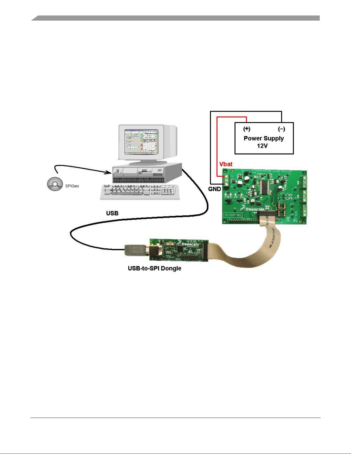
5 EVB Setup Configuration
Figure 2. EVB Setup Configuration Diagram
KIT33903 Evaluation Boards, Rev. 1.0
6 Freescale Semiconductor
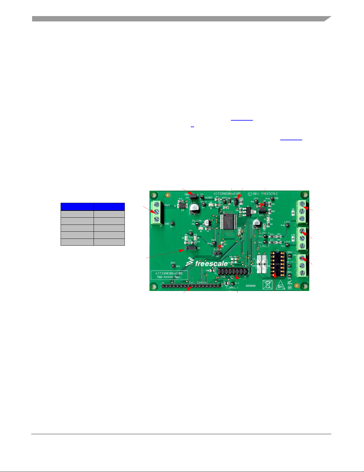
6 Hardware Configuration
JUMPER POSITION
J15 1-2
J22 1-2
J23 OPEN
J27 1-2
J28 OPEN
J9
J22
J2 pSPI ControlJ1 External Control
J23
J27
J12
CAN Termination
(Power)
CAN Bus
J28 J15
CON2
LIN2 Bus
CON1
LIN1 Bus
The KIT33903BD5EVBE/KIT33903BD3EVBE operates with a single 5.5 V minimum power supply and
can be driven with the KITUSBSPIDGLEVME along with its GUI. For added flexibility, it is also possible
to develop a custom board to drive this evaluation board via the 16 pin standard header.
6.1 Board Implementation
For Standard EVB configuration, set up the jumpers as shown on Figure 3. If the jumper configuration is
in accordance with Jumper Connections, on page
ON at startup. If CAN communication will be exerc
the necessary components to implement the chosen CAN Termination as shown on Figure
Hardware Configuration
8, the VDD (D3) and the 5V_CAN (D4) LEDs must be
ised, populate the CAN termination socket (J13) with
4.
Figure 3. Manual Mode Jumper Settings
KIT33903 Evaluation Boards, Rev. 1.0
Freescale Semiconductor 7

Hardware Configuration
6.2 Jumper Connections
Name Description
J15 VDD Status
J22 MUX pin output
J23 I/O0 configuration
J27 DBG configuration
J28 DBG external pull-down resistor configuration
Jumper closed -> LED indicator enabled
Jumper closed -> external 2.4 kohm resistor pull-down to GND implemented
1-2 closed -> 4.7 kohm pull-down resistor to GND and indicator LED implemented
2-3 closed -> 15 kohm pull-up resistor to V
Jumper closed -> SBC runs in debug mode (no need to refresh/monitor watchdog)
J28 MUST be left open
Jumper closed -> 47 kohm pull-down resistor to GND implemented
J27 MUST be left open
and indicator LED implemented
SUP
6.3 CAN Termination Configurations
Figure 4. CAN Termination Configurations via J13 Socket
KIT33903 Evaluation Boards, Rev. 1.0
8 Freescale Semiconductor

6.4 Power Supply and Input/Output Connectors
The three pin terminal block (J9) serves as the main power terminal to supply a minimum of 5.5 V to
operate the KIT33903BD5EVBE/KIT33903BD3EVBE.
The CAN, LIN1, and LIN2 bus signals are accessible through the three pin terminal blocks J12, CON1,
and CON2 respectively.
6.5 Connector J1 – External Control
Pin # Pin Name Description
1 MISO SPI data sent to the MCU. When the CS is high, MISO is high-impedance
2 MOSI SPI data received by the device
3 SCLK Clock input for the Serial Peripheral Interface (SPI) of the device
4 CSB Chip select pin for the SPI. When the CS is low, the device is selected. In Low
Power mode with VDD ON, a transition on CS is a wake-up condition
5 TXDC_I CAN bus transmit data input. Internal pull-up to VDD
6 RXDC CAN bus receive data output
7 I_WAKE_I Active high input to enable on-board FET to create a 5.0 mA load on VDD
8 N/C Not Connected
9 VDD 3.3 V/5.0 V output of the main regulators for the Microcontroller supply
10 INTB_I This output is asserted low when an enabled interrupt condition occurs. The output
is a push-pull structure
11 RSTB_I This is the device reset output whose main function is to reset the MCU. It has an
internal pull-up to VDD. The reset input voltage is also monitored in order to detect
external reset and safe conditions
12 TXDL1 LIN1 bus transmit data input. Includes an internal pull-up resistor to VDD
13 RXDL1 LIN1 bus receive data output
14 TXDL2 LIN bus transmit data input. Includes an internal pull-up resistor to VDD
15 RXDL2 LIN2 bus receive data output
16 GND Ground Termination
Hardware Configuration
KIT33903 Evaluation Boards, Rev. 1.0
Freescale Semiconductor 9

Hardware Configuration
6.6 Connector J2 – SPI Control
Pin # Pin Name Description
1 TXDC CAN bus transmit data input. Internal pull-up to VDD
2 CSB Chip select pin for the SPI. When the CS is low, the device is selected. In Low
3 INTB This output is asserted low when an enabled interrupt condition occurs. The out-
4 MISO SPI data sent to the MCU. When the CS is high, MISO is high-impedance
5 RSTB This is the device reset output whose main function is to reset the MCU. It has an
6 MOSI SPI data received by the device
7 NC No Connect
8 SCLK Clock input for the Serial Peripheral Interface (SPI) of the device
9 NC No Connect
10 NC No Connect
11 I_WAKE Active high input to enable on-board FET to create a 5.0 mA load on VDD
12 NC No Connect
13 NC No Connect
14 NC No Connect
15 NC No Connect
16 GND Ground termination
Power mode with VDD ON, a transition on CS is a wake-up condition
put is a push-pull structure.
internal pull-up to VDD. The reset input voltage is also monitored in order to detect
external reset and safe conditions
6.7 EVB – KITUSBSPIDGLEVME Interconnection
KIT33903BD5EVBE/KIT33903BD3EVBE -J2 USB-to-SPI Dongle Board - I/O PORT
Pin # Pin Name Pin Name Pin #
1 TXDC CNTL2 2
2CSB CSB1
3 INTB CNTL1 4
4MISO SO3
5 RSTB CNTL0 6
6MOSI SI5
7NC DATA48
8 SCLK SCLK 7
9NC DATA310
10 NC CNTL3 9
11 I_WAKE DATA2 12
12 NC VDD 11
13 NC DATA1 14
14 NC REG 3.3V 13
15 NC DATA0 16
16 GND GND 15
KIT33903 Evaluation Boards, Rev. 1.0
10 Freescale Semiconductor

7 Using the EVB
1. Select Install SPIGen (setup.exe) from the CD33903 Start page and follow the on-screen installation
instructions.
2. Connect power supply to the VBAT and GND terminals on the EVB, and build the setup as shown on
Figure 2.
3. Ensure the voltages provided are in accordance with the device data sheet and the supply currents
are sufficient to supply the device.
4. To use SPIGen, go to the Windows Start menu > Programs > SPIGen, and click on the SPIGen
icon. The SPIGen Generic SPI Generator GUI will appear.
5. Go to the Configure menu in the upper left hand corner of the GUI and select Edit Configuration.
6. Select the Enable 33905 Tab in the Part Specific Tabs section on the lower right hand corner of the
GUI and then click OK button.
7. Click the SBC MC3390x Family tab.
8. Select MC33903D in the Device section located on top of the GUI window.
7.1 Using SPIGen with the MC33903 Product
Evaluating all capabilities of the MC33903 product is made easy with the included SPIGen and respective
GUI configuration file.
Using the EVB
KIT33903 Evaluation Boards, Rev. 1.0
Freescale Semiconductor 11

Using the EVB
Device Status and
Flags sections
Flags decodedRead d evice’s Flags
and s tatus
Read Device Mode – keeps
SAFE f unctionality and exits
DE BUG Mod e (overrides
hardware conf ig uratio n)
Adds command
to Sequential Mode
seq uence
Adds all commands on
tab to Sequential Mode
seq uence
7.1.1 Sending Commands to Read Flags Set on SBC
Figure 5. SPIGen Graphical User Interface (Commands and Flags Decoded)
1. In the Re
flags as shown in Figure
2. Click any of the read device flag status op
3. Click SEQ to add
12 Freescale Semiconductor
gisters and Flags tab, click Flag High and Low sub tab to read the device status and clear
5.
tions.
commands to the Sequential Mode window.
KIT33903 Evaluation Boards, Rev. 1.0

Using the EVB
General Flags
Opt ions to send SPI co mmands
Regist ers
Hexadecimal value of SPI
co mmand sent and received
Send a Simple Wat chdog
‘Go to No rmal Mo de’ co mmand
Sto res com mands sent
in a text f ile
Read General Flags
Dev ice St atus and
Flags sections
Adds all commands on
tab to Sequential Mode
seq uence
Check to Auto Read all
f lags every 500ms
Device status
decoded
Register bits [7:0]
of corresponding
tab address
(bit s [15:8] no t sho wn)
Device Selection
Function to be written
of corresponding tab
Send command as conf igured
to correspo nding t ab add ress
Read d evice st atus and
enabled func tio nality
Ad ds com mand
to Sequential Mode
seq uence
7.1.2 Reading and Writing Commands to Exercise SBC and Acquire Its Status
Freescale Semiconductor 13
Figure 6. SPIGen Graphical User Interface (Commands and Device Status)
1. In the Regist
and enabled functionality as shown in Figure
2. Initialize the registers by clicking one of the options Init V
and then click WRITE.
3. Click WD Refresh t
4. Click Mo
ers and Flags tab, click Register address high (b7=1) sub tab to read device status
6.
reg / Init Wdog / Init Lin-I/O / Init MISC
o go to Normal mode and then click Single WD Write Command.
de+RM to go to low power mode and then click WRITE.
KIT33903 Evaluation Boards, Rev. 1.0

Using the EVB
Device Status and
Flags sections
Device Status decoded
Adds command
to Sequential Mode
sequence
Adds all commands on
tab to Sequential Mode
sequence
Read device status and
enabled f unctio nality
Read Device Mode – keeps
SAFE f unctionality and exits
DE BUG Mod e (overrides
hardware co nf iguratio n)
7.1.3 Sending Commands to Acquire the Configuration of the SBC
Figure 7. SPIGen Graphical User Interface (Commands and Device Configuration)
1. In the Regist
2. Click any of the read device flag status op
3. Click SEQ to add
14 Freescale Semiconductor
ers and Flags tab, click Register address low (b7=0) sub tab as shown in Figure 7.
tions.
commands to the Sequential Mode window.
KIT33903 Evaluation Boards, Rev. 1.0

7.1.4 Sequential Mode
Options to send SPI commands
Hexadecimal value of SPI
co mmand s ent and receiv ed
Sto res commands s ent
in a text f ile
Inserts a wait t im e in
millisecond increments
Removes selected lines
from list of commands
Allows user to loop
bet ween selec ted
co mmand lines
Runs loop enabled
sequence or single
sweep of command s
Sto res commands s ent
in a text f ile
Clears all co mmands from list
Allows user to load
list of co mmands in
text f ile f ormat
Allows us er to change Hex adec imal
or delay time value
Commands sent and
received fro m the SBC’s
MOSI and MISO pins
Using the EVB
Figure 8. SPIGen Graphical User Interface (Sequential Mode)
1. Click Seque
shown in Figure
2. In the Insert W
3. Click Remov
4. Select Loo
5. Click Run to activa
6. Click Save to
7. Click Loa
8. Click Clear li
ntial Mode tab. This window displays all commands in the Sequential Mode sequence as
8.
ait text box, enter a wait time in millisecond increments.
e Selected Line to remove selected lines from the list of commnads.
p Enable option to allow loop between selected lines.
te the loop enabled sequence or single sweep of commands.
store commands sent in a text file.
d to load list of commands in text file format.
sts to clear all commands from the list.
9. Enter a value in the text box and click Ch
value.
ange Value to change the hexadecimal or the delay time
Freescale Semiconductor 15
KIT33903 Evaluation Boards, Rev. 1.0

Using the EVB
Options to send SPI commands
Hexadecimal value of SPI
co mmand s ent and receiv ed
Auto read function for
co ntinuous devic e
mode status
Pre-co nfigured selec table
initialization and enabling
of dev ice’s f eatures
(Mouse over f or
Informat ion)
Auto mated stat e diagram
(Mouse over f or
information)
7.1.5 Automated State Diagram Mode
Figure 9. SPIGen Graphical User Interface (Automated State Diagram Mode)
1. Click Diagram ta
2. Select Normal Mode
shown in Figure
3. Click Init Mode to
4. Click Normal Mode to
5. Click Low
b.
option to enable auto read function for continuous device mode status as
9.
initialize selected registers.
go to normal mode and enable selected registers.
Power Vdd OFF/ON to go to low power mode with selected wake ups.
16 Freescale Semiconductor
KIT33903 Evaluation Boards, Rev. 1.0

5
5
4
4
3
3
2
2
1
1
D
D
C
C
B B
A A
I_WAKE_I
TXDC_I
INTB_I
RSTB_I
I_WAKE_I
Vsup
I_WAKE
LIN2
VDD
DBG
Vsup
IO0
DBG
LINT2
VB
CANH
SPLIT
LIN2
CSB
MISO
LINT1
MOSI
RSTB_I
SCLK
IO0
TXDC_I
LIN1
INTB_I
MOSI
RXDC
VE
SCLK
RSTB_I
MISO
CANH
CSB
VDD
CANL
INTB_I
TXDL1
SPLIT
Vbat
SPLIT
RXDL1
TXDC
VE
TXDL1
CSB
LINT1
RSTB
Vsense
LIN1
RXDL1
CANL
Vsense
MOSI
TXDL2
TXDL2
VDD
INTB
MISO
RXDL2
SPLIT
Vsup
SCLK
CANH
RXDL2
TXDC_I
VB
CANL
LINT2
RXDC
I_WAKE_I
GND
GND
GND GND
GND
GND
GND
GND
GND
GND
GND
GND
GND
GND
GND
GND
GND
GND
GNDGND GND
GND
GND
GND
GND
Drawing Title:
veRrebmuN tnemucoDeziS
teehS:etaD
of
Page Title:
ICAP Classication: FCP: FIUO: PUBI:
A3
__X____
Drawing Title:
veRrebmuN tnemucoDeziS
teehS:etaD
of
Page Title:
A3
__X____
Drawing Title:
veRrebmuN tnemucoDeziS
teehS:etaD
of
Page Title:
KIT33903D5EKEVBE
A3
EVB SCHEMATIC
__X____
VDD VAUX Support
StandardSplit No
IO Pin Support
)01()01()5( (5)
GND
GND
CANL
SPLITSPLIT(2)
(1)
CANH
(7)
(4)
(13)
(11)
(8)
(14)
DBG Pin Support
External MCU Control
GND
GND
USB-SPI Dongle Control
CANL
SPLITSPLIT
CANH
(14)
(13)
(11)
(8)(7)
(4)
(2)
(1)
(10)(5)
GND
SPLIT
GND
CANH CANL
SPLIT
(4)
(2)
(1)
(8)(7)
(13)
(11)
(14)
Socked supported CAN termination options
LIN Channels
R25
47K
R25
47K
R17 2.4KR17 2.4K
R2 2.2KR2 2.2K
D4
RED LEDD4RED LED
2
1
TP4TP4
J27
HDR 1X2
J27
HDR 1X2
1
2
R26
10K
R26
10K
D5
MMSZ8V2T1GD5MMSZ8V2T1G
2 1
R29 3.3KR29 3.3KR28
22K
R28
22K
TP6TP6
C1
0.1 UFC10.1 UF
TP12TP12
C11C11
R33 0R33 0
R12
60.4
R12
60.4
CON1
PCB 3WAY 250V/16A
CON1
PCB 3WAY 250V/16A
A
1
B
2
C
3
U1
MC33903DU1MC3390
SAFE5DBG
13
RST
23
INT
24
MOSI
27
SCLK
26
MISO
28
CS
25
I/O0
12
MUX
11
5V_CAN
6
TXD_LIN_120RXD_LIN_121LIN_TERM_14LIN_119TXD_LIN_214RXD_LIN_216LIN_TERM_2
3
LIN_2
17
TXD_CAN
30
RXD_CAN
31
CANH
7
CANL
8
SPLIT
10
GND1
15
GND2
18
GND_CAN
9
EXPAD
33
VSUP
2
VSENSE
22
VDD
29
VE32VB
1
D1
MBRS140D1MBRS140
2 1
D13
1N4148WS
D13
1N4148WS
21
J12
PCB 3WAY 250V/16A
J12
PCB 3WAY 250V/16A
A1B
2
C
3
+
C5
22UF+C5
22UF
CON2
PCB 3WAY 250V/16A
CON2
PCB 3WAY 250V/16A
A
1
B
2
C
3
TP8TP8
J9
PCB 3WAY 250V/16A
J9
PCB 3WAY 250V/16A
A1B
2
C
3
TP14TP14
C9
xxpF
50VC9xxpF
50V
+
C21 2.2 UF+C21 2.2 UF
C10
xxpF
50V
C10
xxpF
50V
D9
RED LEDD9RED LED
21
R16 4.7KR16 4.7K
R32 0R32 0
E
B
C
Q1
BCP52-16
E
B
C
Q1
BCP52-16
1
32
4
R31 0R31 0
D3
RED LEDD3RED LED
2 1
R3 2.2KR3 2.2K
R11
330
R11
330
TP9TP9
J1
HDR_1X16J1HDR_1X16
1
1
22334
4
55667
7
889
9
10101111121213
13
14
14
15
15
16
16
C15C15
C16C16
C12C12
J28
HDR 1X2
J28
HDR 1X2
1
2
TP3TP3
J13
DIP14
J13
DIP14
IO1
1
IO8
8
IO14
14
IO77IO4
4
IO11
11
IO22IO33IO5
5
IO6
6
IO9
9
IO10
10
IO1212IO13
13
C20
0.1 UF
C20
0.1 UF
D10
RED LED
D10
RED LED
2 1
R15 1KR15 1K
R271KR27
1K
R241KR24
1K
Q3
MMBF0201NLT1G
Q3
MMBF0201NLT1G
1
2 3
TP5TP5
J22
HDR 1X2
J22
HDR 1X2
1
2
TP11TP11
R231KR23
1K
R18
4.7K
R18
4.7K
C14C14
+
C2
10UF
50V+C2
10UF
50V
TP10TP10
TP7TP7
R13
60.4
R13
60.4
D14
1N4148WS
D14
1N4148WS
21
TP13TP13
R30 0R30 0
J15
HDR 1X2
J15
HDR 1X2
1
2
J23
HDR_1X3
J23
HDR_1X3
1
2
3
TP1TP1
C17C17
TP19TP19
R14 120R14 120
TP21TP21
D8
RED LEDD8RED LED
21
J2
HDR_2X8J2HDR_2X8
1
2
3 4
65
7
8910
11 12
13 14
15 16
C6
0.1 UFC60.1 UF
TP17TP17
TP15TP15
R19
15K
R19
15K
C13C13
TP16TP16
8 Schematic Drawing
Schematic Drawing
Freescale Semiconductor 17
Figure 10. Schematic Drawing
KIT33903 Evaluation Boards, Rev. 1.0

Board Layout
9 Board Layout
9.1 Assembly Drawing
9.2 Top Side Layer
Figure 11. Assembly Drawing
Figure 12. Top Side Layer
KIT33903 Evaluation Boards, Rev. 1.0
18 Freescale Semiconductor

9.3 Bottom Side Layer
Board Layout
Figure 13. Bottom Side Layer
KIT33903 Evaluation Boards, Rev. 1.0
Freescale Semiconductor 19

Evaluation Board Bill of Material
10 Evaluation Board Bill of Material
Item Qty Schematic Label Value Description Ven der Mfg. PN
1 4 CON1, CON2, J9, J12 PCB 3WAY 250V/16A CON 3 TB TH 5MM SN CAMDEN ELEC-
2 3 C1, C6, C20 0.1 UF CAP CER 0.1UF 50V 10% X7R 0805 KEMET C0805C104K5RAC
3 1 C2 10UF CAP ALEL 10UF 50V 20% SMT (CASE D) PANASONIC EEE1HA100SP
TRONICS LTD
CTB5000/3
4 1 C5 22UF CAP ALEL 22UF 16V 20% -- CASE C
5 2 C9, C10 xxpF
6 1 C11 1000PF CAP CER 1000PF 50V 5% C0G 1206 AVX 12065A102JAT2A
7 6 C12, C13, C14, C15,
8 1 C21 2.2 UF CAP ALEL 2.2UF 35V 20% -- SMT PANASONIC EEEFC1V2R2R
9 1 D1 MBRS140 DIODE SCH PWR RECT 1A 40V SMB ON SEMICONDUC-
10 5 D3, D4, D8, D9, D10 RED LED LED RED SGL 30MA SMT 0805 LUMEX SML-LXT0805IW-TR
11 1 D5 MMSZ8V2T1G DIODE ZNR -- 0.5W 8.2V SOD123 ON SEMICONDUC-
12 2 D13, D14 1N4148WS DIODE SW 150MA 53V SOD-323 DIODES INC 1N4148WS-7-F
13 1 J1 HDR_1X16 HDR 1X16 TH 100MIL SP 330H AU SAMTEC TSW-116-07-S-S
14 1 J2 HDR_2X8 HDR 2X8 TH 100MIL CTR 330H AU SAMTEC TSW-108-07-G-D
15 1 J13 DIP14 SKT DIP 14 PINS TH 3M ICE-143-S-TG30
16 4 J15, J22, J27, J28 HDR 1X2 HDR 1X2 TH 100MIL SP 330H SN SAMTEC TSW-102-07-T-S
17 1 J23 HDR_1X3 HDR 1X3 TH 100MIL SP 330H AU SAMTEC HTSW-103-07-S-S
18 1 Q1 BCP52-16 TRAN PNP PWR 1A 60V SOT-223 PHILIPS SEMICON-
19 1 Q3 MMBF0201NLT1G TRAN NMOS PWR 0.3A 20V SOT23 ON SEMICONDUC-
20 2 R2, R3 2.2K RES MF 2.2K 1/8W 5% 0805 BOURNS CR0805-JW-222ELF
21 1 R11 330 RES MF 330 OHM 1/8W 5% 0805 VISHAY INTER-
22 2 R12, R13 60.4 RES MF 60.4 1/10W 1% 0603 KOA SPEER RK73H1JTTD60R4F
23 1 R14 120 RES MF 120 OHM 1/8W 5% 0805 KOA SPEER RK73B2ATTD121J
24 3 R15, R23, R24 1K RES TF 1.0K 1/8W 5% RC0805 BOURNS CR0805JW102E
25 2 R16, R18 4.7K RES MF 4.7K 1/8W 5% 0805 VENKEL COMPANY CR0805-8W-472JT
26 1 R17 2.4K RES MF 2.4K 1/8W 1% 0805 YAGEO AMERICA 232273462402L
27 1 R19 15K RES MF 15K 1/8W 5% 0805 BOURNS CR0805JW153ELF
28 1 R26 10K RES TF 10K 1/8W 5% RC0805 BOURNS CR0805JW103E
29 1 R25 47K RES TF 47K 1/8W 5% RC0805 BOURNS CR0805JW473E
30 1 R27 1K RES TF 1.00K 1/8W 1% RC0805 BOURNS CR0805FX1001E
31 1 R28 22K RES MF 22K 1/8W 5% 0805 BOURNS CR0805-JW-223ELF
32 1 R29 3.3K RES MF 3.3K 1/8W 5% 0805 BOURNS CR0805-JW-332ELF
33 6 R30, R31, R32, R33,
34 18 TP1, TP3, TP4, TP5,
C16, C17
R34, R35
TP6, TP7, TP8, TP9,
TP10, TP11, TP12,
TP13, TP14, TP15,
TP16, TP17, TP19, TP21
56PF CAP CER 56PF 50V 5% C0G 1206 KEMET C1206C560J5GACT
0 RES MF ZERO OHM 1/8W -- 0805 BOURNS CR0805-J/-000ELF
TEST POINT BLACK TEST POINT PIN .100 X .45 BLACK TH COMPONENTS
SMT
PANASONIC EEE1CA220SR
U
TOR
TOR
DUCTOR
TOR
TECHNOLOGY
CORPORATION
MBRS140T3G
MMSZ8V2T1G
BCP52-16
MMBF0201NLT1G
CRCW0805330RJNE
A
TP-105-01-00
Freescale IC
35 1 U1 MC33903D IC XCVR CAN DUAL LIN 40-1000KBPS
4.4-40V SOIC54
FREESCALE SEMICONDUCTOR
MCZ33903BD3EK
MCZ33903BD5EK
Freescale does not assume liability, endorse or warrant components from external manufacturers that are referenced in circuit drawings or
tables. While Freescale offers component recommendations in this configuration, it is the customer’s responsibility to validate their
applications.
KIT33903 Evaluation Boards, Rev. 1.0
20 Freescale Semiconductor

References
11 References
Following are URLs where you can obtain information on other Freescale products and application
solutions:
Description URL
Data Sheet www.freescale.com/files/analog/doc/data_sheet/MC33903_4_5.pdf
Fact Sheet www.freescale.com/files/analog/doc/fact_sheet/MC33903_4_5FS.pdf
Application Note www.freescale.com/files/analog/doc/app_note/AN3865.pdf
Errata http://www.freescale.com/files/analog/doc/errata/MC33903_4_5ER.pdf
SPIGen www.freescale.com/files/soft_dev_tools/software/device_drivers/SPI-
Gen.html
Freescale’s Web Site www.freescale.com
Freescale’s Analog Web Site www.freescale.com/analog
Freescale’s Power Management Web Site www.freescale.com/powermanagement
Freescale’s Automotive Applications Web Site www.freescale.com/automotive
KIT33903 Evaluation Boards, Rev. 1.0
Freescale Semiconductor 21

How to Reach Us:
Home Page:
www.freescale.com
Web Support:
http://www.freescale.com/support
USA/Europe or Locations Not Listed:
Freescale Semiconductor, Inc.
Technical Information Center, EL516
2100 East Elliot Road
Tempe, Arizona 85284
1-800-521-6274 or +1-480-768-2130
www.freescale.com/support
Europe, Middle East, and Africa:
Freescale Halbleiter Deutschland GmbH
Technical Information Center
Schatzbogen 7
81829 Muenchen, Germany
+44 1296 380 456 (English)
+46 8 52200080 (English)
+49 89 92103 559 (German)
+33 1 69 35 48 48 (French)
www.freescale.com/support
Japan:
Freescale Semiconductor Japan Ltd.
Headquarters
ARCO Tower 15F
1-8-1, Shimo-Meguro, Meguro-ku,
Tokyo 153-0064
Japan
0120 191014 or +81 3 5437 9125
support.japan@freescale.com
Asia/Pacific:
Freescale Semiconductor China Ltd.
Exchange Building 23F
No. 118 Jianguo Road
Chaoyang District
Beijing 100022
China
+86 10 5879 8000
support.asia@freescale.com
For Literature Requests Only:
Freescale Semiconductor Literature Distribution Center
P.O. Box 5405
Denver, Colorado 80217
1-800-441-2447 or +1-303-675-2140
Fax: +1-303-675-2150
LDCForFreescaleSemiconductor@hibbertgroup.com
Information in this document is provided solely to enable system and
software implementers to use Freescale Semiconductor products. There are
no express or implied copyright licenses granted hereunder to design or
fabricate any integrated circuits or integrated circuits based on the
information in this document.
Freescale Semiconductor reserves the right to make changes without further
notice to any products herein. Freescale Semiconductor makes no warranty,
representation or guarantee regarding the suitability of its products for any
particular purpose, nor does Freescale Semiconductor assume any liability
arising out of the application or use of any product or circuit, and specifically
disclaims any and all liability, including without limitation consequential or
incidental damages. “Typical” parameters that may be provided in Freescale
Semiconductor data sheets and/or specifications can and do vary in different
applications and actual performance may vary over time. All operating
parameters, including “Typicals”, must be validated for each customer
application by customer’s technical experts. Freescale Semiconductor does
not convey any license under its patent rights nor the rights of others.
Freescale Semiconductor products are not designed, intended, or authorized
for use as components in systems intended for surgical implant into the body,
or other applications intended to support or sustain life, or for any other
application in which the failure of the Freescale Semiconductor product could
create a situation where personal injury or death may occur. Should Buyer
purchase or use Freescale Semiconductor products for any such unintended
or unauthorized application, Buyer shall indemnify and hold Freescale
Semiconductor and its officers, employees, subsidiaries, affiliates, and
distributors harmless against all claims, costs, damages, and expenses, and
reasonable attorney fees arising out of, directly or indirectly, any claim of
personal injury or death associated with such unintended or unauthorized
use, even if such claim alleges that Freescale Semiconductor was negligent
regarding the design or manufacture of the part.
Freescale™ and the Freescale logo are trademarks of
Freescale Semiconductor, Inc. All other product or service names
are the property of their respective owners.
© Freescale Semiconductor, Inc. 2011. All rights reserved.
KT33903UG
Rev. 1.0
9/2011
 Loading...