

Page 1
Freescale Semiconductor
Document Number: KT33882UG
User’s Guide
KIT33882EKEVB Evaluation Board
Rev. 1.0, 12/2014
© Freescale Semiconductor, Inc., 2014. All rights reserved.
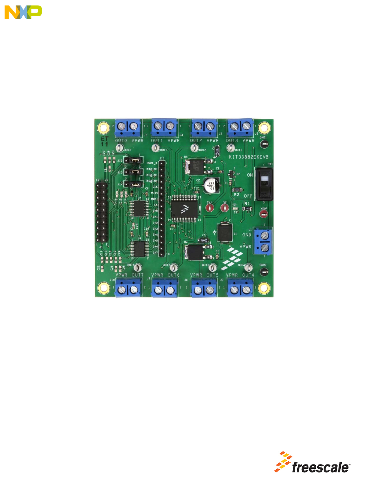
Figure 1. KIT33882EKEVB
Page 2

Table of Contents
1 Important Notice . . . . . . . . . . . . . . . . . . . . . . . . . . . . . . . . . . . . . . . . . . . . . . . . . . . . . . . . . . . . . . . . . . . . . . . . . . . . . . . . . . . . . . . . . . . . . . . . 3
2 Getting Started . . . . . . . . . . . . . . . . . . . . . . . . . . . . . . . . . . . . . . . . . . . . . . . . . . . . . . . . . . . . . . . . . . . . . . . . . . . . . . . . . . . . . . . . . . . . . . . . . 4
3 Getting to Know the Hardware . . . . . . . . . . . . . . . . . . . . . . . . . . . . . . . . . . . . . . . . . . . . . . . . . . . . . . . . . . . . . . . . . . . . . . . . . . . . . . . . . . . . . 5
4 Freedom Development Platform . . . . . . . . . . . . . . . . . . . . . . . . . . . . . . . . . . . . . . . . . . . . . . . . . . . . . . . . . . . . . . . . . . . . . . . . . . . . . . . . . . . 12
5 Installing the Software and Setting up the Hardware . . . . . . . . . . . . . . . . . . . . . . . . . . . . . . . . . . . . . . . . . . . . . . . . . . . . . . . . . . . . . . . . . . . 13
6 Schematic . . . . . . . . . . . . . . . . . . . . . . . . . . . . . . . . . . . . . . . . . . . . . . . . . . . . . . . . . . . . . . . . . . . . . . . . . . . . . . . . . . . . . . . . . . . . . . . . . . . . 17
7 Silkscreens . . . . . . . . . . . . . . . . . . . . . . . . . . . . . . . . . . . . . . . . . . . . . . . . . . . . . . . . . . . . . . . . . . . . . . . . . . . . . . . . . . . . . . . . . . . . . . . . . . . 18
8 Bill of Materials . . . . . . . . . . . . . . . . . . . . . . . . . . . . . . . . . . . . . . . . . . . . . . . . . . . . . . . . . . . . . . . . . . . . . . . . . . . . . . . . . . . . . . . . . . . . . . . . 20
9 References . . . . . . . . . . . . . . . . . . . . . . . . . . . . . . . . . . . . . . . . . . . . . . . . . . . . . . . . . . . . . . . . . . . . . . . . . . . . . . . . . . . . . . . . . . . . . . . . . . . 22
10 Revision History . . . . . . . . . . . . . . . . . . . . . . . . . . . . . . . . . . . . . . . . . . . . . . . . . . . . . . . . . . . . . . . . . . . . . . . . . . . . . . . . . . . . . . . . . . . . . . 23
2 Freescale Semiconductor, Inc.
KT33882UG, Rev. 1.0
Page 3

1 Important Notice
Freescale provides the enclosed product(s) under the following conditions:
This evaluation kit is intended for use of ENGINEERING DEVELOPMENT OR EVALUATION PURPOSES
ONLY. It is provided as a sample IC pre-soldered to a printed circuit board to make it easier to access inp uts,
outputs, and supply terminals. This EVB may be used with any development system or other source of I/O
signals by simply connecting it to the host MCU or computer board via off-the-shelf cables. This EVB is not a
Reference Design and is not intended to represent a final design recommendation for any particular
application. Final device in an application will be heavily dependent on proper printed circuit board layout and
heat sinking design as well as attention to supply filtering, transient suppression, and I/O signal quality.
The goods provided may not be complete in terms of required design, marketing, and or manufacturing related
protective considerations, including product safety measures typically found in the end product incorporating
the goods. Due to the open construction of the product, it is the user's responsibility to take any and all
appropriate precautions with regard to electrostatic discharge. In order to minimize risks associated with the
customers applications, adequate design and operating safeguards mu st be provided by the customer to
minimize inherent or procedural hazards. For any safety concerns, contact Freescale sales and technical
support services.
Should this evaluation kit not meet the specifications indicated in the kit, it may be returned within 30 days from
the date of delivery and will be replaced by a new kit.
Freescale reserves the right to make changes without further notice to any products herein. Freescale makes
no warranty, represent ation or guarantee regarding the suitability of its products for any particular purpose, nor
does Freescale assume any liability arising out of the application or use of any product or circuit, and
specifically disclaims any and all liability, including without limitation consequential or incidental damages.
"Typical" parameters can and do vary in different applications and actual performance may vary over time. All
operating parameters, including "Typical", must be validated for each customer application by customer's
technical experts.
Freescale does not convey any license under its patent rights nor the rights of others. Freescale products are
not designed, intended, or authorized for use as components in systems intended for surgical implant into the
body, or other applications intended to support or sustain life, or for any other application in which the failure
of the Freescale product could create a situation where personal injury or death may occur.
Should the buyer purchase or use Freescale products for any such unintended or unauthorized a pplication,
the buyer shall indemnify and hold Freescale and its officers, employees, subsidiaries, affiliates, and
distributors harmless against all claims, costs, damages, and expenses, and reasonable attorney fees arising
out of, directly or indirectly, any claim of personal injury or death associated with such unintended or
unauthorized use, even if such claim alleges that Freescale was negligent regarding the design or manufacture
of the part. Freescale™ and the Freescale logo are trademarks of Freescale Semic onductor, Inc. All other
product or service names are the property of their respective owners.
© Freescale Semiconductor, Inc. 2014.
Important Notice
Freescale Semiconductor 3
KT33882UG, Rev. 1.0
Page 4

Getting Started
2 Getting Started
2.1 Kit Contents/Packing List
The KIT33882EKEVB contents include:
• Assembled and tested evaluation board/module in an anti-static bag
• Quick Start Guide, Analog Tools
• One 20-pin ribbon cable
• Warranty card
2.2 Jump Start
Freescale’s analog product development boards help to easily evaluate Freescale products. These tools support analog mixed signal and
power solutions including monolithic ICs using proven high-volume SMARTMOS mixed signal technology , and system-in-package devices
utilizing power, SMARTMOS and MCU dies. Freescale products enable longer battery life, smaller form factor , component count reduction,
ease of design, lower system cost and improved performance in powering state of the art systems.
•Go to www.freescale.com/analogtools
• Locate your kit
• Review your Tool Summary Page
• Look for
• Download documents, software, and other information
Once the files are downloaded, review the user guide in the bundle. The user guide includes setup instructions, BOM and schematics.
Jump start bundles are available on each tool summary page with the most relevant and current information. The information includes
everything needed for design.
2.3 Required Equipment and Software
To use this kit, you need:
• Power supply
• Oscilloscope (preferably 4-channel) with current probe(s)
• Digital multimeter
• FRDM-KL25Z Development Platform
• Typical loads (solenoid valves and brushed DC motors up to 1 A each)
2.4 System Requirements
The kit requires the following to function properly with the software:
• USB-enabled PC with Windows® XP or higher
4 Freescale Semiconductor, Inc.
KT33882UG, Rev. 1.0
Page 5

Getting to Know the Hardware
3 Getting to Know the Hardware
3.1 Board Overview
The KIT33882EKEVB evaluation board is an easy-to-use circuit board that allows the user to exercise all the functions of the MC33882
Smart Six Output Switch (0.3
There are two ways to communicate with the evaluation board:
1. A PC communicates with the evaluation board through a FRDM SPI Dongle (FSD), connected to the PC's USB port, or
2. the microcontroller on the FRDM-KL25Z communicates with the evaluation board via microcontroller code.
The Freescale SPIGen 7.0.1 or higher program provides the user interface to the MC33882 SPI port and allows the user to send
commands to the IC and receive statuses from the IC.
The Freescale CodeWarrior IDE allows the user to program the FRDM-KL25Z board with microcontroller code to send commands to the
IC and receive statuses from the IC.
Ohm R
3.2 Board Features
This evaluation kit features the MC33882 Smart Six Output Switch (0.3 Ohm R
Six Output Low-side Switch able to control system loads up to 1.0 A. The six outputs can be controlled via both serial peripheral interface
(SPI) and parallel input control, making the device attractive for fault tolerant system applications. There are two additional 30
switches with SPI diagnostic reporting (parallel input control only).
The PCB contains a board to FRDM-KL25Z connector, which allows the FRDM-KL25Z to act as either a FSD or simply as an access to
the KL25Z microcontroller. The board's main features are as follows:
• Output terminals for loads
• Test points for various inputs, outputs, and SPI signals
• FSD connector
) with SPI and Parallel Input Control.
DS(on)
) with SPI and Parallel Input Control, which is a Smart
DS(on)
mA low-side
3.3 FRDM-KL25Z Features
The FRDM-KL25Z board features are as follows:
• MKL25Z128VLK4 MCU - 48 MHz, 128 KB Flash, 16 KB SRAM, USB OTG (FS), 80 LQFP
• Capacitive touch slider, MMA8451Q accelerometer, Tri-color LED
• Flexible power supply options - USB, coin cell battery, external source
• Easy access to MCU I/O
• Battery-ready, power-measurement access points
• Form factor compatible with Arduino™ R3 pin layout
• New, OpenSDA debug interface
• Mass storage device flash programming interface (default) - no tool installation required to evaluate demonstration
applications
• P&E Debug interface provides run-control debugging and compatibility with IDE tools
• CMSIS-DAP interface: new ARM standard for embedded debug interface
Additional reference documents are available on freescale.com/FRDM-KL25Z.
Freescale Semiconductor 5
KT33882UG, Rev. 1.0
Page 6
Getting to Know the Hardware
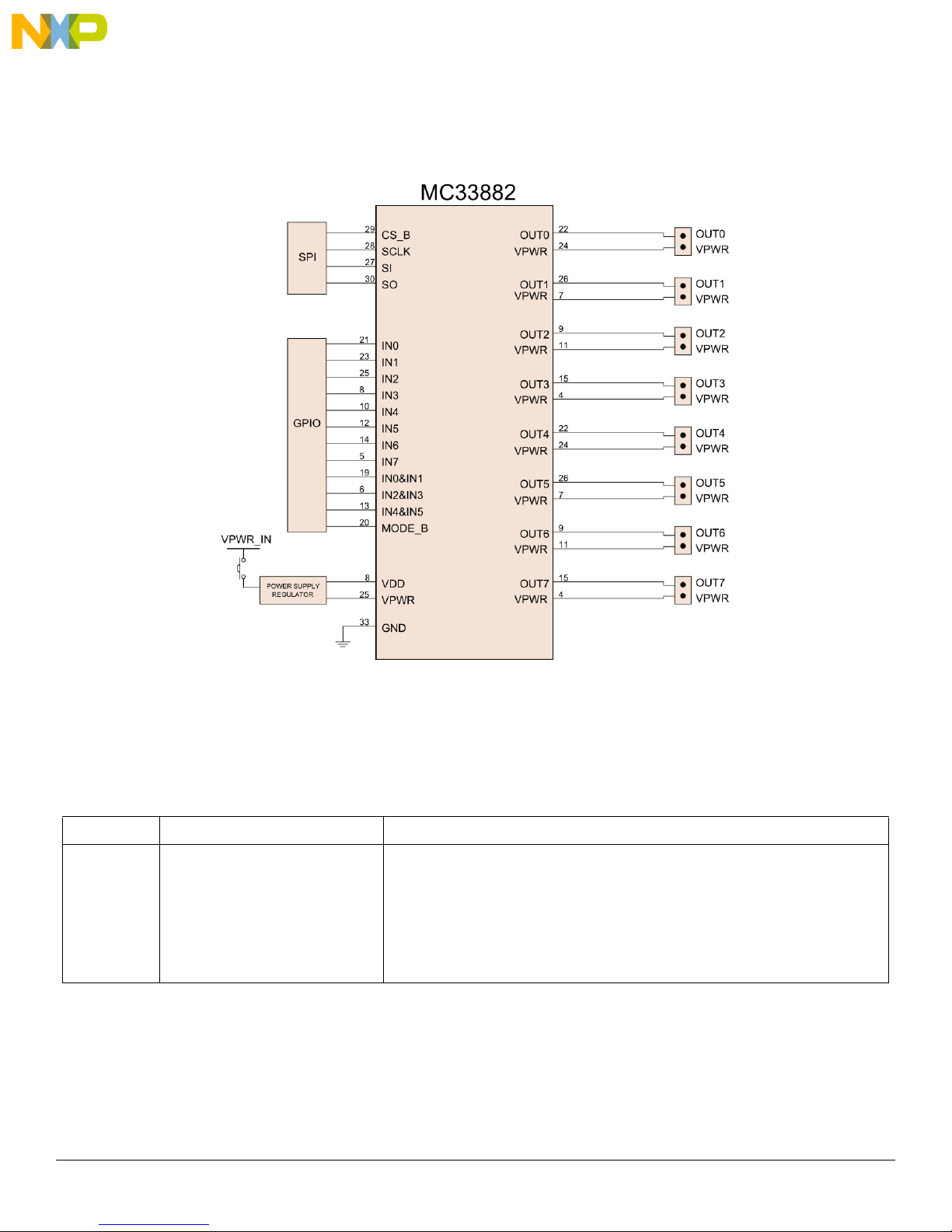
3.4 Block Diagram
This evaluation board consists of an MC33882 Smart Six Output Switch (0.3 Ohm R
level system block diagram (Figure 2) outlines the way Freescale standard products are used to implement a low-side switch.
with SPI and Parallel Input Control. The high
DS(on))
Figure 2. Block Diagram
3.4.1 Device Features
This evaluation board features the following Freescale product:
Table 1. MC33882 Device Features
Device Description Features
MC33882 Smart Six Output Low-side Switch
• Outputs clamped for switching inductive loads
• Very low operational bias currents (< 2.0 mA)
• CMOS input logic compatible with 5.0 V logic levels
• Robust load dump (60 V transient at VPWR on OUT0 - OUT5)
• Daisy chain operation of multiple devices possible
• Switch outputs can be paralleled for higher currents
•R
• SPI operation guaranteed to 2.0 MHz
of 0.4 Ohm per output (25 °C) at 13 V VPWR
DS(on)
6 Freescale Semiconductor, Inc.
KT33882UG, Rev. 1.0
Page 7
Getting to Know the Hardware
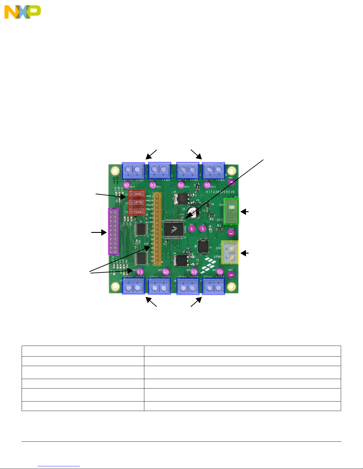
Power and Ground Inputs
ON/OFF Switch
FSD Connector
Dual IN Function
Selection Jumpers
Test points
Output Terminals
Output Terminals
MC33882
3.5 Board Description
The analog part consists of the MC33882 chip controlling external loads. The digital part consists of the KL25Z controlling the MC33882
by SPI and I/Os.
This evaluation board is meant to demonstrate how the MC33882 can control eight low-side switches.
Power is provided to the board via a VPWR/GND screw terminal (J1). Power can be disconnected from the board via an onboard switch
(SW1). If power is ON, LED D3 will light up. The VDD input of the device can only accept 5.0 V. However, on-board level shifters are
provided to shift 3.3
The evaluation board provides a 20-pin connector (J2) to be used with the FRDM board. The connector J2 on the FRDM board connects
to J2 on the evaluation board. The outputs of the switches are routed to independent 2-position screw terminals that have both one output
and VPWR available (J3 through J10).
The evaluation board also includes several test points. A 16-pin row of pins allows access to all incoming signals. These sixteen signals
are the following: MODE_B, IN4&IN5, IN2&IN3, IN0&IN1, CLK, MISO, MOSI, CS, IN0, IN1, IN2, IN3, IN4, IN5, IN6, and IN7. Eight loop
test points provide access to the OUT0 through OUT7 signals. Two ground test points (GND1 and GND2) are available, as are three power
test points (3V3, 5V, and VPWR).
V levels up to 5 V. Note the KL25Z FSD uses a 3.3 V microcontroller.
Table 2. Board Description
Dual IN Function Selection Jumpers
Power and Ground Inputs • Provides connection points for power and ground
Name Description
Output Terminals • Provides connection points for loads
FSD Connector • Allows a FSD to be connected to the evaluation board via a 20-pin ribbon cable
Test Points
Freescale Semiconductor 7
Figure 3. Board Description
• Allows the FSD to control one of two different signals (See Jumper Definitions on page 1 1
for more information)
• Provides test points for various signals (See Test Point Definitions on page 8 for more in-
formation)
KT33882UG, Rev. 1.0
Page 8
Getting to Know the Hardware
Table 2. Board Description (continued)
Name Description
ON/OFF Switch • Allows the board to be disconnected from power easily
MC33882 • Six output low-side switch with SPI and parallel input control
3.6 LED Display
The following LED is provided as a visual output device for the KIT33882EKEVB evaluation board:
1. LED D3 indicates when VPWR is present
3.7 Test Point Definitions
The following test points provide access to signals on the MC33882 IC:
Table 3. Test Point Definitions
Schematic Label Name Description
J11/1 MODE_B Mode pin for device
J11/2 IN4&IN5 Dual output control for IN4 and IN5
J11/3 IN2&IN3 Dual output control for IN2 and IN3
J11/4 IN0&IN1 Dual output control for IN0 and IN1
J11/5 CLK SPI clock
J11/6 MISO SPI MISO (Master Input, Slave Output)
J11/7 MOSI SPI MOSI (Master Output, Slave Input)
J11/8 CS SPI chip select
J11/9 IN0 Parallel input control for IN0
J11/10 IN1 Parallel input control for IN1
J11/11 IN2 Parallel input control for IN2
J11/12 IN3 Parallel input control for IN3
J11/13 IN4 Parallel input control for IN4
J11/14 IN5 Parallel input control for IN5
J11/15 IN6 Parallel input control for IN6
J11/16 IN7 Parallel input control for IN7
TEST POINT VPWR VPWR
TEST POINT 3.3 V 3.3 V
TEST POINT 5.0 V 5.0 V
TEST POINT GND Ground
TEST POINT OUT0 OUT0
TEST POINT OUT1 OUT1
TEST POINT OUT2 OUT2
TEST POINT OUT3 OUT3
TEST POINT OUT4 OUT4
TEST POINT OUT5 OUT5
TEST POINT OUT6 OUT6
TEST POINT OUT7 OUT7
3.8 Input Signal Definitions
The MC33882 IC has twelve input signals that are used to control certain outputs or functions inside the circuit. These signals are:
Table 4. Input Signal Definitions
Schematic Label Name Description
MODE_B MODE_B Mode pin for device
IN4&IN5 IN4&IN5 Dual output control for IN4 and IN5
IN2&IN3 IN2&IN3 Dual output control for IN2 and IN3
8 Freescale Semiconductor, Inc.
KT33882UG, Rev. 1.0
Page 9

Getting to Know the Hardware
Table 4. Input Signal Definitions (continued)
Schematic Label Name Description
IN0&IN1 IN0&IN1 Dual output control for IN0 and IN1
IN0 IN0 Parallel input control for IN0
IN1 IN1 Parallel input control for IN1
IN2 IN2 Parallel input control for IN2
IN3 IN3 Parallel input control for IN3
IN4 IN4 Parallel input control for IN4
IN5 IN5 Parallel input control for IN5
IN6 IN6 Parallel input control for IN6
IN7 IN7 Parallel input control for IN7
3.9 Output Signal Definitions
The MC33882 IC has eight output signals that are used to control various devices and outputs on the evaluation board. These signals are:
Table 5. Output Signal Definitions
Schematic Label Name Description
OUT0 OUT0 Controls OUT0
OUT1 OUT1 Controls OUT1
OUT2 OUT2 Controls OUT2
OUT3 OUT3 Controls OUT3
OUT4 OUT4 Controls OUT4
OUT5 OUT5 Controls OUT5
OUT6 OUT6 Controls OUT6
OUT7 OUT7 Controls OUT7
3.10 USB/SPI Dongle Connector
This is a 20-pin, 0.1" center, dual-row connector designed to interface directly to the FSD unit. The FRDM-KL25Z SPI dongle connector
consists of the following 20 pins (J2 on FRDM-KL25Z).
T able 6: USB/SPI Dongle Pin Description
Pin Number FSD Name EVB Name Description
1 DATA0 DATA0 Connected to IN0 or IN4&IN5 via a jumper
2 SPI1-CSB <NC> <unused>
3 DATA1 DATA1 Connected to IN1
4 SPI1-CLK <NC> <unused>
5 DATA2 DATA2 Connected to IN2 or IN2&IN3 via a jumper
6 SPI0-CSB SPI0_CSB SPI signal - Chip Select Bar
7 DATA3 DATA3 Connected to IN3
8 SPI0-MOSI SPI0_MOSI SPI signal - Serial In
9 DATA4 DATA4 Connected to MODE_B
10 SPI0-MISO SPI0_MISO SPI signal, Serial Out
11 CTRL0 CNTL0 Connected to IN4 or IN0&IN1 via a jumper
12 SPI0-CLK SPI0_CLK SPI signal - Serial Clock
13 CTRL1 CNTL1 Connected to IN5
Freescale Semiconductor 9
KT33882UG, Rev. 1.0
Page 10

Getting to Know the Hardware
Power and Ground Inputs
FSD Connector
Output Terminals
Output Terminals
Table 6: USB/SPI Dongle Pin Description (continu ed)
14 GND GROUND Signal Ground
15 <NC> <NC> NC
16 VREFH <NC> <unused>
17 SPI1-MISO <NC> <unused>
18 CTRL3 CNTL3 CNTL3 - connected to IN7
19 CTRL2 CNTL2 CNTL2 - connected to IN6
20 SPI1-MOSI <NC> <unused>
3.11 Screw Terminal Connections
The KIT33882EKEVB board features screw terminal connections to allow easy access to the MC33882 signals and supply rails. Figure 4
shows the board locations and names of the screw terminals.
3.12 Input and Output Evaluation Connectors
There is one input connector which provides the following signals:
Table 7. Input Connectors
Pin Schematic Signal
1
2GND
10 Freescale Semiconductor, Inc.
Figure 4. Connector Designations
J1
KT33882UG, Rev. 1.0
VPWR
Page 11

There are eight output connectors which provide the following signals:
Table 8. Output Connectors
Pin Schematic Signal
1
2OUT0
1
2OUT1
1
2OUT2
1
2OUT3
1
2OUT4
1
2OUT5
1
2OUT6
1
2OUT7
J3
J4
J5
J6
J7
J8
J9
J10
VPWR
VPWR
VPWR
VPWR
VPWR
VPWR
VPWR
VPWR
Getting to Know the Hardware
3.13 Jumper Definitions
The following table defines the evaluation board jumper positions and explains their functions.
Table 9. Jumper Table
Jumper Description
J12
J13
J14
Determines if the signal from DATA0 goes to IN0 or IN4&IN5
Determines if the signal from DATA2 goes to IN2 or IN2&IN3
Determines if the signal from CNTL0 goes to IN4 or IN0&IN1
The following table defines the jumper configurations for the three communication modes of the device.
Table 10. Jumper Configurations
Mode/Function Controls Jumpers (J12, J13, J14) DATA4 (MODE_B)
Dual IN Control
IN Control
SPI Control
0&1, 2&3, 4&5 Position 2-3 HIGH
0, 1, 2, 3, 4, 5, 6, 7 Position 1-2 LOW
0, 1, 2, 3, 4, 5 X LOW
Default
Setting
1-2 The output of DATA0 is routed to IN0
1-2 The output of DATA2 is routed to IN2
1-2 The output of CNTL0 is routed to IN4
Setting Connection
2-3 The output of DATA0 is routed to IN4&IN5
2-3 The output of DATA2 is routed to IN2&IN3
2-3 The output of CNTL0 is routed to IN0&IN1
Freescale Semiconductor 11
KT33882UG, Rev. 1.0
Page 12

Freedom Development Platform
4 Freedom Development Platform
The KIT33882EKEVB kit may be used with the FSD (see Figure 5), which provides a USB-to-SPI interface. This small board makes use
of the USB, SPI and parallel ports built into Freescale's KL25Z microcontroller. The main function provided by this dongle is to allow
Freescale evaluation kits that have a parallel port to communicate via a USB port to a PC. It can also be used as a regular microcontroller
board if not configured as a SPI dongle.
Figure 5. FRDM-KL25Z Interface Dongle
4.1 Using the FRDM-KL25Z as a FSD
First, the MSD-DEBUG-FRDM-KL25Z_Pemicro_v114.SDA file must be loaded to the FRDM-KL25Z board. This is accomplished by
plugging the mini-USB cable into the SDA USB port on the FRDM-KL25Z while holding down the reset button. The green LED should be
flashing. The MSD-DEBUG-FRDM-KL25Z_Pemicro_v114.SDA file must then be drag and dropped onto the BOOTLOADER drive in
Windows Explorer. The FRDM-KL25Z should be unplugged after the file has been transferred. The mini-USB cable must then be plugged
back into the SDA USB port on the FRDM-KL25Z. The FSD srec file can then be drag and dropped onto the FRDM-KL25Z drive in
Windows Explorer. To use the FRDM-KL25Z as a FSD, the mini-USB cable must be plugged into the KL25Z USB port.
4.2 Using the FRDM-KL25Z as a Microcontroller Board
4.2.1 Using the FRDM-KL25Z Sample Code Drag/Drop File
First, the MSD-DEBUG-FRDM-KL25Z_Pemicro_v114.SDA file must be loaded to the FRDM-KL25Z board. This is accomplished by
plugging the mini-USB cable into the SDA USB port on the FRDM-KL25Z while holding down the reset button. The green LED should be
flashing. The MSD-DEBUG-FRDM-KL25Z_Pemicro_v114.SDA file must then be drag and dropped onto the BOOTLOADER drive in
Windows Explorer. The FRDM-KL25Z should be unplugged after the file has been transferred. The mini-USB cable must then be plugged
back into the SDA USB port on the FRDM-KL25Z. The sample code srec file found in the SPIGen website can then be drag and dropped
onto the FRDM-KL25Z drive in Windows Explorer. To use the FRDM-KL25Z with this sample code, the mini-USB cable must be plugged
into the KL25Z USB port.
4.2.2 Using the FRDM-KL25Z with Custom CodeWarrior Code
First, the MSD-DEBUG-FRDM-KL25Z_Pemicro_v114.SDA file must be loaded to the FRDM-KL25Z board. This is accomplished by
plugging the mini-USB cable into the SDA USB port on the FRDM-KL25Z while holding down the reset button. The green LED should be
flashing. The MSD-DEBUG-FRDM-KL25Z_Pemicro_v114.SDA file must then be drag and dropped onto the BOOTLOADER drive in
Windows Explorer. The FRDM-KL25Z should be unplugged after the file has been transferred. To use the FRDM-KL25Z as a
programmable microcontroller with CodeWarrior, the mini-USB cable must be plugged into the SDA USB port. Sample code for this kit is
available at the kit’s website.
12 Freescale Semiconductor, Inc.
KT33882UG, Rev. 1.0
Page 13

Installing the Software and Setting up the Hardware
5 Installing the Software and Setting up the Hardware
5.1 Installing SPIGen Freeware on your Computer
The latest version of SPIGen is designed to run on any Windows 8, Windows 7, Vista or XP-based operating system. To install the
software, go to www.freescale.com/a nalogtools and select your kit. Click on that link to open the corresponding T ool Summary Page. Look
for “Jump Start Your Design”. Download to your computer desktop the SPIGen software as well as the associated configuration file.
Run the install program from the desktop. The Installation Wizard guides you through the rest of the process.
To use SPIGen, go to the Windows Start menu, then Programs, then SPIGen, and click on the SPIGen icon. The SPIGen Graphic User
Interface (GUI) appears. Go to the file menu in the upper left hand corner of the GUI, and select “Open”. In the file selection window that
appears, set the “Files of type:” drop-down menu to “SPIGen Files (*.spi)”. (As an exceptional case, the file name may have a .txt
extension, in which case you should set the menu to “All Files (*.*)”.) Next, browse for the configuration file you saved on your desktop
earlier and select it. Click “Open”, and SPIGen creates a specially configured SPI command generator for your evaluation board.
The GUI is shown in Figure 6. The text at the top is the name of the configuration file loaded. The left side panel displays folders that group
user interfaces. The process of loading the configuration file has assigned a list of “Extra Pins” as well as a list “Quick Commands”, all of
which are board-specific.
5.2 Installing CodeWarrior on your Computer
This procedure explains how to obtain and install the latest version of CodeWarrior 10.5 or greater.
Notes: The sample software in this kit requires CodeWarrior 10.5 or greater. If CodeWarrior 10.5 or greater is already on your system,
the steps in this section can be skipped.
1. Obtain the latest CodeWarrior 10.5 (or greater) installer file from freescale.com/codewarrior.
2. Run the executable file and follow the instructions.
During the installation, there is a request to select components to install. This kit requires Kinetis which also must be installed. User must
install at least the Kinetis component. Select Kinetis and click on "Next" to complete the installation.
Freescale Semiconductor 13
Figure 6. SPIGen GUI
KT33882UG, Rev. 1.0
Page 14

Installing the Software and Setting up the Hardware
Figure 7. Choose Components GUI
14 Freescale Semiconductor, Inc.
KT33882UG, Rev. 1.0
Page 15

5.3 Configuring the Hardware
Note: Pictured loads are examples only
Installing the Software and Setting up the Hardware
Figure 8. KIT33882EKEVB plus FRDM-KL25Z Board Setup
5.3.1 Step-by-step Instructions for Setting up the Hardware using SPIGen
In order to perform the demonstration examples, first set up the evaluation board hardware and software as follows:
1. Ready the computer, install the SPIGen software. Make sure the FRDM board has been flashed with the correct SPIGen
srec file.
2. Connect the FRDM-KL25Z board to the KIT33882EKEVB evaluation board via th e 20-pin ribbon cable. The
FRDM-KL25Z board must have a 20-pin male header soldered onto the top of the FRDM-KL25Z board in J2.
3. Connect the mini USB cable between the FRDM-KL25Z board and the PC (use the KL25Z port, not the SDA port).
4. Attach the DC power supply (without turning on the power) to the VPWR/GND terminal (J1).
5. If desired, attach loads to the output terminals on the board (J3 through J10).
6. Launch SPIGen and load the .spi configuration file from the kit's website and open it in SPIGen.
7. Turn on the power supply and switch SW1 to the ON position.
8. Send various commands via SPIGen using the predefined sequences available.
Notes: Due to the limited number of available FSD I/O signals, several jumpers (J12 through J14) are available that control where DAT A0,
DATA2, and CNTL0 are routed. They can be used for either IN0, IN2, and IN4 or IN4&IN5, IN2&IN3, and IN0&IN1, respectively.
Freescale Semiconductor 15
KT33882UG, Rev. 1.0
Page 16

Installing the Software and Setting up the Hardware
5.3.2 Step-by-step Instructions for Setting up the Hardware using Sample Flash
File
1. Ready the computer. Only a USB port to provide power is required. (Make sure the FRDM board has been flashed with
the correct srec file).
2. Connect the FRDM-KL25Z board to the KIT33882EKEVB evaluation board via th e 20-pin ribbon cable. The
FRDM-KL25Z board must have a 20-pin male header soldered onto the top of the FRDM-KL25Z board in J2.
3. Connect the mini USB cable between the FRDM-KL25Z board and the PC (use the KL25Z port, not the SDA port).
4. Attach the DC power supply (without turning on the power) to the VPWR/GND terminal (J1).
5. If desired, attach loads to the output terminals on the board (J3 through J10).
6. Turn on the power supply and switch SW1 to the ON position.
7. The flashed program will run automatically.
Notes: The sample code does not use the dual input signals (IN0&IN1, IN2&IN3, and IN4&IN5), so jumpers J12 through J14 must be set
to the 1-2 configuration.
5.3.3 Step-by-step Instructions for Setting up the Hardware using CodeW ar rior
1. Ready the computer, install the CodeWarrior software.
2. Connect the FRDM-KL25Z board to the KIT33882EKEVB evaluation board via th e 20-pin ribbon cable. The
FRDM-KL25Z board must have a 20-pin male header soldered onto the top of the FRDM-KL25Z board in J2.
3. Connect the mini USB cable between the FRDM-KL25Z board and the PC (use the SDA port, not the KL25Z port).
4. Attach the DC power supply (without turning on the power) to the VPWR/GND terminal (J1).
5. If desired, attach loads to the output terminals on the board (J3 through J10).
6. Launch CodeWarrior and either load the sample project or create your own bareboard project.
7. Turn on the power supply and switch SW1 to the ON position.
8. You can now program the board and debug your code.
Notes: Due to the limited number of available FSD I/O signals, several jumpers (J12 through J14) are available that control where DAT A0,
DATA2, and CNTL0 are routed. They can be used for either IN0, IN2, and IN4 or IN4&IN5, IN2&IN3, and IN0&IN1, respectively . However,
these jumpers can be avoided and all signals may be connected to the FRDM-KL25Z if they are wired by hand from different pins on the
FRDM-KL25Z connectors.
16 Freescale Semiconductor, Inc.
KT33882UG, Rev. 1.0
Page 17

Schematic
5
5
4
4
3
3
2
2
1
1
D D
C C
B B
A A
MCZ33882PEK
POWER SUPPLY REGULATOR
HOLES
CONNECTORS
MCU
TEST POINTS
LEVEL SHIFTERS
FRDM INTERFACE
CAPS
VPWR_IN
OUT0
OUT1
OUT4
OUT5
OUT2
OUT3
OUT6
OUT7
SPI0_CSB
SPI0_MOSI
SPI0_MISO
SPI0_CLK
DATA4
CNTL0
CNTL1
CNTL2
CNTL3
DATA0
DATA2
DATA3
IN0
IN1
IN2
IN3
IN4
IN5
IN6
IN7
OUT0
OUT1
OUT2
OUT3
OUT4
OUT5
OUT6
OUT7
CS
CLK
MISO
MOSI
IN0&IN1
IN2&IN3
IN4&IN5
MODE_B
CLK
MISO
IN0&IN1
IN2&IN3
IN4&IN5
MODE_BCSMOSI
IN0
IN1
IN2
IN3
IN4
IN5
IN6
IN7
VPWR_IN
DATA4
DATA2_B
CNTL0_B
SPI0_CLK
SPI0_MISO
SPI0_MOSI
SPI0_CSB
CNTL2
CNTL1
CNTL0_A
CNTL3
DATA3
DATA2_A
DATA1
DATA0_A
OUT0
OUT1
OUT2
OUT3
OUT4
OUT5
OUT6
OUT7
DATA0_B
CNTL0_B
DATA2_B
DATA0_B
DATA2_A
DATA0_A
CNTL0_A
DATA0
DATA2
CNTL0
5V
VBAT
3V3
5V
5V3V3
3V3
3V3
5V
3V3
VBAT
VBAT
VBAT
VBAT
VBAT VBAT
VBAT
VBAT
VBAT
VBAT5V3V3
Drawing Title:
Size Document Number Rev
Date: Sheet
of
Page Title:
ICAP Classification: FCP: FIUO: PUBI:
SCH-28477 PDF: SPF28477 A
KIT33882EKEVB
C
Thursday, August 07, 2014
GROWL 3
11
___ ___
X
Drawing Title:
Size Document Number Rev
Date: Sheet
of
Page Title:
ICAP Classification: FCP: FIUO: PUBI:
SCH-28477 PDF: SPF28477 A
KIT33882EKEVB
C
Thursday, August 07, 2014
GROWL 3
11
___ ___
X
Drawing Title:
Size Document Number Rev
Date: Sheet
of
Page Title:
ICAP Classification: FCP: FIUO: PUBI:
SCH-28477 PDF: SPF28477 A
KIT33882EKEVB
C
Thursday, August 07, 2014
GROWL 3
11
___ ___
X
C13
10nF
DNP
C23
10nF
DNP
C6
0.1UF
C17
10nF
DNP
J4
OSTTC022162
1
2
C11
0.1UF
C8
0.1UF
J7
OSTTC022162
1
2
J10
OSTTC022162
1
2
D3
LED GREEN
AC
OUT6
C24
10nF
DNP
R2 1.0K
J11
HDR_1X16
11223344556677889910101111121213131414151516
16
BH1
SMTSO-M1.6-2.25ET
C12
0.1UF
OUT0
+
C2
10UF
OUT4
C14
10nF
DNP
C9
0.1UF
C18
10nF
DNP
C10
0.1UF
OUT2
C25
10nF
DNP
D1
STPS3L60S
A C
U3
TXB0108
VCCA
2
A11A23A34A4
5
GND
11
OE
10
B416B317B218B120VCCB
19
A56A67A78A8
9
B812B713B614B5
15
VPWR_1
J5
OSTTC022162
1
2
+
C3
10UF
3V3
J8
OSTTC022162
1
2
GND2
J12
HDR 1X3
1
2
3
SW1
25136N
1 2 3
BH3
SMTSO-M1.6-2.25ET
C26
10nF
DNP
C15
10nF
DNP
MC33882
U1
CS
29
GND_EP
33
GND1
1
GND2
16
GND3
17
GND4
32
IN0
21
IN0/IN1
19
IN123IN2
25
IN2/IN3
6
IN38IN4
10
IN4/IN5
13
IN512IN614IN7
5
MODE
20
NC_2
2
NC_31
31
OUT022OUT124OUT226OUT37OUT49OUT511OUT615OUT7
4
SCLK28SI27SO
30
VDD
3
VPWR
18
+
C4
10UF
C19
10nF
DNP
5V_1
R1
1.0K
U2
TXB0108
VCCA
2
A11A23A34A4
5
GND
11
OE
10
B416B317B218B120VCCB
19
A56A67A78A8
9
B812B713B614B5
15
BH4
SMTSO-M1.6-2.25ET
U5
LP2950CDT
OUT
3
IN
1
GND
2
J13
HDR 1X3
1
2
3
C27
10nF
DNP
OUT7
J3
OSTTC022162
1
2
OUT5
J6
OSTTC022162
1
2
U4
LM2931DT-5.0
OUT
3
IN
1
GND
4
J2
1 2
3 4657 8
9 10
11 12
13 14
15 16
17 18
19 20
J9
OSTTC022162
1
2
C16
10nF
DNP
OUT3
C20
10nF
DNP
C28
10nF
DNP
J14
HDR 1X3
1
2
3
GND1
C22
10nF
DNP
C5
0.1UF
C1
10nF
OUT1
BH2
SMTSO-M1.6-2.25ET
C21
10nF
DNP
C7
0.1UF
D2
MMBZ27VCLT1
2
1
3
J1
OSTTC022162
1
2
6 Schematic
Freescale Semiconductor 17
Figure 9. Schematic
KT33882UG, Rev. 1.0
Page 18

Silkscreens
7 Silkscreens
7.1 Silkscreen Top
18 Freescale Semiconductor, Inc.
KT33882UG, Rev. 1.0
Page 19

7.2 Silkscreen Bottom
Silkscreens
Notes: This image is an exception to the standard top-view mode of representation used in this document. It has been flipped to show a
bottom view.
Freescale Semiconductor 19
KT33882UG, Rev. 1.0
Page 20

Bill of Materials
8 Bill of Materials
Table 11. Bill of Materials
Item
Active Components
1 1 U1 IC LIN SW LOW SIDE SIX
Other Components
2 2 U2, U3 IC VXLTR 8BIT BIDIR 15 KV ESD
3 1 U4 IC VREG LDO 5 V 100 MA
4 1 U5 IC VREG LDO 3.3 V 100 MA 30 V
Capacitors
5 1 C1 0.01 F CAP CER 0.01 F 50 V 5% X7R
6 1 C2 10 F CAP ALEL 10 F 50 V 20% SMT
7 2 C3, C4 10 F CAP TANT 10 F 10 V 10% --
8 8 C5, C6, C7, C8, C9, C10, C11, C12 0.1 F CAP CER 0.1 F 50 V 10% X7R
9 16 C13, C14, C15, C16, C17, C18,
Diodes
Qty Schematic Label Value Description Part Number Assy Opt
C19, C20, C21, C22, C23, C24,
C25, C26, C27, C28
(1)
OUTPUT 5 V SOIC32
1.2 V- 3.6 V/1.65 V- 5.5 V
TSSOP20
5.0 - 40 V DPACK
TO -252343 H SN 100 L
0603
(CASE D)
3216-18
0603
0.01 F CAP CER 0.01 F 50 V 5% X7R
0603
MC33882PEK
TXB0108PWR
LM2931DT-5.0G
LP2950CDT-3.3/NOPB
06035C103JAT2A
EEE1HA100SP
293D106X9010A2TE3
GRM188R71H104KA93D
06035C103JAT2A
(3)
(2)
10 1 D1 DIODE SCH RECT 3 A 60 V SMC STPS3L60S
11 1 D2 DIODE ZNR TVS -- 27 V/40 W
12 1 D3 LED GRN SGL 20 MA 0603 LG L29K-G2J1-24-Z
Switches, Connectors, Jumpers and Test Points
13 2 GND1, GND2 TEST POINT BLK 70X220 MIL TH 5006
14 9 J1, J3, J4, J5, J6, J7, J8, J9, J10 CON 1X2 TB 5.08 MM SP 406 H
15 1 J2 HDR 2X10 TH 100MIL CTR 343 H
16 1 J11 HDR 1X16 TH 100 MIL SP 330 H
17 3 J12,J13,J14 HDR 1x3 TH 100 MIL SP 343 H SN
18 8 OUT1, OUT2, OUT3, OUT4, OUT5,
OUT6, OUT7, OUT0
20 Freescale Semiconductor, Inc.
SOT23
SN 138 L
SN 100 L
AU 100 L
100 L
TEST POINT WHITE 70X220 MIL TH5007
KT33882UG, Rev. 1.0
MMBZ27VCLT1G
OSTTC022162
TSW-110-07-T-D
TSW-116-07-S-S
TSW-103-07-T-S
Page 21

Bill of Materials
Table 11. Bill of Materials
19 1 SW1 SW SPDT SLD 125 V 4 A TH 25136NAH
20 3 VPWR_1, 3V3, 5V_1 TEST POINT RED 70X220 MIL TH 5005
Resistors
21 2 R1, R2 1.0 K RES MF 1.00 K 1/4 W 1% 1206 CRCW12061K00FKEA
Notes:
1. Freescale does not assume liability, endorse, or warrant components from external manufacturers that are referenced in circuit drawings or tables.
While Freescale offers component recommendations in this configuration, it is the customer’s responsibility to validate their application.
2. Do not populate.
3. Critical components. For critical components, it is vital to use the manufacturer listed.
(1)
(continued)
Freescale Semiconductor 21
KT33882UG, Rev. 1.0
Page 22

References
9 References
Following are URLs where you can obtain information on related Freescale products and application solutions:
Freescale.com
Description URL
Support Pages
KIT33882EKEVB Tool Summary Page
MC33882 Product Summary Page
FRDM-KL25Z
SPIGen
CodeWarrior
Freescale
Development Platform
Software
Software
http://www.freescale.com/webapp/sps/site/prod_summary.jsp?code=KIT33882EKEVB
http://www.freescale.com/webapp/sps/site/prod_summary.jsp?code=MC33882
http://www.freescale.com/webapp/sps/site/prod_summary.jsp?code=FRDM-KL25Z
http://www.freescale.com/files/soft_dev_tools/software/device_drivers/SPIGen.html
http://www.freescale.com/webapp/sps/site/homepage.jsp?code=CW_HOME&tid=vanCODEWARRIOR
9.1 Support
Visit www.freescale.com/support for a list of phone numbers within your region.
9.2 Warranty
Visit www.freescale.com/warranty for a list of phone numbers within your region.
22 Freescale Semiconductor, Inc.
KT33882UG, Rev. 1.0
Page 23

10 Revision History
Revision Date Description of Changes
Revision History
1.0
12/2014 • Initial Release
Freescale Semiconductor 23
KT33882UG, Rev. 1.0
Page 24

How to Reach Us:
Home Page:
freescale.com
Web Support:
freescale.com/support
Information in this document is provided solely to enable system an d soft ware implemen ters to use Freescale product s.
There are no express or implied copyright licenses granted hereunder to design or fabricat e any integrated circuits based
on the information in this document.
Freescale reserves the right to make changes without further notice to any products herein. Freescale makes no
warranty, representation, or guarantee regarding the suitability of its products for any particular purpose, nor doe s
Freescale assume any liability arising out of the application or use of any product or circuit, and specifically disclaims any
and all liability, including without limitation consequential or incidental damages. “Typical” parameters that may be
provided in Freescale data sheets and/or specifications can and do vary i n different app lications, and actual performance
may vary over time. All operating parameters, including “typicals,” must be validated for each customer application by
customer’s technical experts. Freescale does not convey any license under its patent rights nor the rights of others.
Freescale sells products pursuant to stan dard terms and conditions of sale, which can be found at the following address:
freescale.com/SalesTermsandConditions.
Freescale and the Freescale logo are trademarks of Freescale Semiconductor, Inc., Reg. U.S. Pat. & Tm. Off.
SMARTMOS is a trademark of Freescale Semiconductor , Inc. A ll other product or service names are the property of their
respective owners.
© 2014 Freescale Semiconductor, Inc.
Document Number: KT33882UG
Rev. 1.0
12/2014
 Loading...