

Page 1
Freescale Semiconductor
Document Number: KT33810UG
User’s Guide
KIT33810EKEVME Evaluation Board
User’s Guide
Rev. 3.0, 5/2010
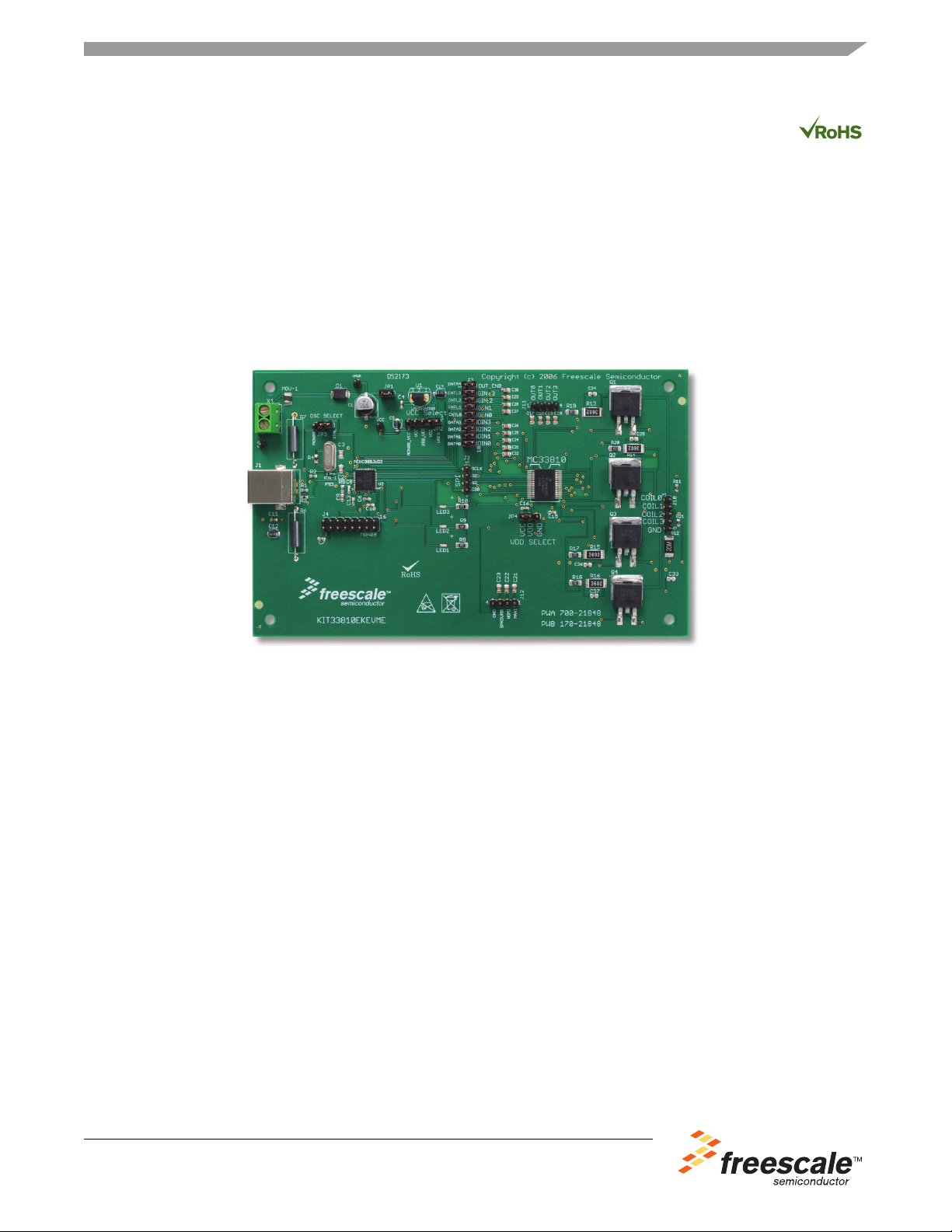
Figure 1. KT33810 Evaluation Board
Table of Contents
1 Important Notice..................................................................................................................................................... 2
2 Introduction............................................................................................................................................................. 3
3 Schematic............................................................................................................................................................... 9
4 KIT33810EKEVME Bill of Material ......................................................................................................................... 10
© Freescale Semiconductor, Inc., 2010. All rights reserved.
Page 2

Important Notice
1 Important Notice
Freescale provides the enclosed product(s) under the following conditions:
This evaluation kit is intended for use of ENGINEERING DEVELOPMENT OR EVALUATION PURPOSES ONLY. It
is provided as a sample IC pre-soldered to a printed circuit board to make it easier to access inputs, outputs, and
supply terminals. This EVB may be used with any development system or other source of I/O signals by simply
connecting it to the host MCU or computer board via off-the-shelf cables. This EVB is not a Reference Design and is
not intended to represent a final design recommendation for any particular application. Final device in an application
will be heavily dependent on proper printed circuit board layout and heat sinking design as well as attention to supply
filtering, transient suppression, and I/O signal quality.
The goods provided may not be complete in terms of required design, marketing, and or manufacturing related
protective considerations, including product safety measures typically found in the end product incorporating the
goods. Due to the open construction of the product, it is the user's responsibility to take any and all appropriate
precautions with regard to electrostatic discharge. In order to minimize risks associated with the customers
applications, adequate design and operating safeguards must be provided by the customer to minimize inherent or
procedural hazards. For any safety concerns, contact Freescale sales and technical support services.
Should this evaluation kit not meet the specifications indicated in the kit, it may be returned within 30 days from the
date of delivery and will be replaced by a new kit.
Freescale reserves the right to make changes without further notice to any products herein. Freescale makes no
warranty, representation or guarantee regarding the suitability of its products for any particular purpose, nor does
Freescale assume any liability arising out of the application or use of any product or circuit, and specifically disclaims
any and all liability, including without limitation consequential or incidental damages. “Typical” parameters can and
do vary in different applications and actual performance may vary over time. All operating parameters, including
“Typical”, must be validated for each customer application by customer’s technical experts.
Freescale does not convey any license under its patent rights nor the rights of others. Freescale products are not
designed, intended, or authorized for use as components in systems intended for surgical implant into the body, or
other applications intended to support or sustain life, or for any other application in which the failure of the Freescale
product could create a situation where personal injury or death may occur. Should Buyer purchase or use Freescale
products for any such unintended or unauthorized application, Buyer shall indemnify and hold Freescale and its
officers, employees, subsidiaries, affiliates, and distributors harmless against all claims, costs, damages, and
expenses, and reasonable attorney fees arising out of, directly or indirectly, any claim of personal injury or death
associated with such unintended or unauthorized use, even if such claim alleges that Freescale was negligent
regarding the design or manufacture of the part.Freescale™ and the Freescale logo are trademarks of Freescale
Semiconductor, Inc. All other product or service names are the property of their respective owners. © Freescale
Semiconductor, Inc., 2010. All rights reserved.
KIT33810EKEVME Evaluation Board User’s Guide, Rev. 3.0
2 Freescale Semiconductor
Page 3

2 Introduction
The KIT33810EKEVME Evaluation Board (EVB) is an easy-to-use circuit board that allows the user to exercise all
functions of the MC33810 circuit. The EVB communicates to a PC through a built in USB port. The Freescale SPIGen
program provides the User Interface to the MC33810’s SPI port and allows the user to send commands to and
receive error messages from the IC. The MC33810 contains four, low side, injector drivers and four custom ignition
IGBT drivers (which can also be configured as General Purpose MOSFET Gate drivers) . The IGBTs and the
associated current and voltage sensing circuits are included on the board to provide a complete working system,
capable of driving actual injectors and ignition coils directly.
Introduction
KIT33810EKEVME Evaluation Board User’s Guide, Rev. 3.0
Freescale Semiconductor 3
Page 4
Introduction
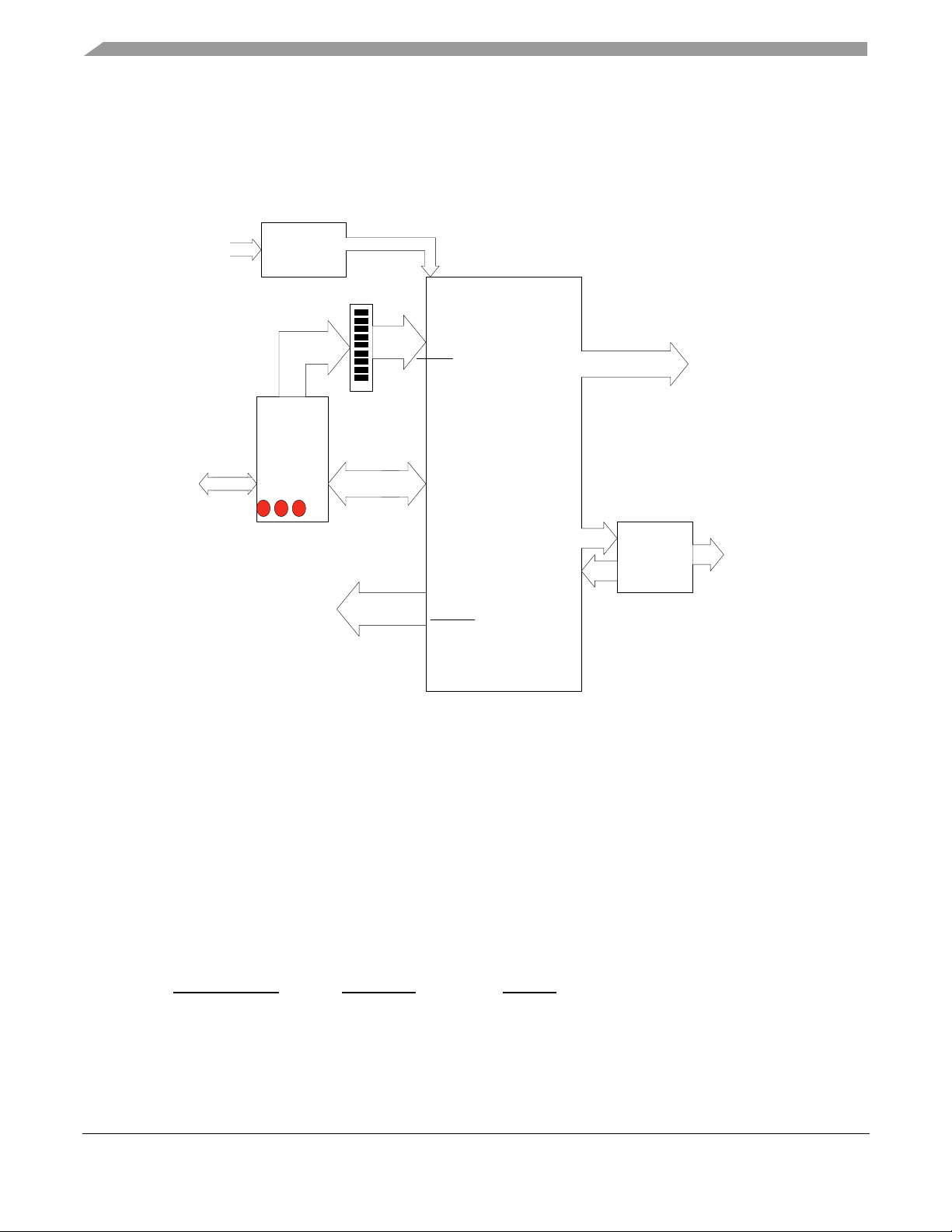
The Block Diagram for the 33811 Evaluation Board is shown below:
VBat
USB FROM/
TO PC
Voltage Regulat or and
Power Con diti oning
9 parall el
control lines
USB
To SPI
LEDs
TO MCU
Jumpers
SO, SI , CSB,
SCLK
2
VPWR,
MC33810
VDD
9
DI N1-3
GI N1- 3
OUTE N
OUT1- 3
4
Injectors
SPI
4
Por t
Spark Coils
4
GD1- 3
4
FB1-3
NOMI
3
MAXI
RSP, RSN
IGBTs (4)
And I/V Sense
6
Ignition
Ci rcu it r y
SPKDUR
Figure 1. EVB Block Diagram
The EVB consists of a 33810 Injector, Ignition Driver (IID) circuit, a USB to SPI interface, a voltage regulator and
power conditioning circuit, a set of 9 Input Jumpers, and 4 IGBTs with voltage and current sensing circuitry. All 5 volt
power required by the EVB is obtained from either the USB, MON08 connectors or the on-board 5 Volt regulator . A
5 position jumper selects which source provides the 5 volt power for VCC (and VDD).
LED DISPLAY
The LED’s are provided as a visual output device for the USB-SPI interface. As configured from the factory, LED 2
indicates when power is applied and a USB connection is established, and LED 1 and 3 are tied to the DATA0 and
CNTL0 lines, respectively, which can be toggled via the SPIGen program.
I/O JUMPER DEFINITIONS (J3)
The EVB contains nine jumpers that connect the parallel outputs of the USB SPI interface to the 33810 inputs as
follows:
USB-SPI Output 33810 Input Function
DATA0 DIN0 Injector Input 0
DATA1 DIN1 Injector Input 1
DATA2 DIN2 Injector Input 2
KIT33810EKEVME Evaluation Board User’s Guide, Rev. 3.0
4 Freescale Semiconductor
Page 5

DATA3 DIN3 Injector Input 3
CNTL0 GIN0 Ignition Input 0
CNTL1 GIN1 Ignition Input 1
CNTL2 GIN2 Ignition Input 2
CNTL3 GIN3 Ignition Input 3
DATA4 OUTEN
If the user prefers to supply the DIN and GIN signals externally, other than from the USB-SPI Interface, the jumpers
can be removed and connections can be made to the open pins.
VCC SELECT JUMPER DEFINITIONS (JP2)
JP2 is a 5 pin, 4 position jumper that determines the source of the VCC voltage. The VCC voltage is a 5 volt supply
that is used by the USB to SPI MCU and the 33810 (VDD). The 5 volts can be supplied from three different sources:
1) An internal 5 Volt regulator connected to VBAT (12 Volts)
2) Directly from the USB Connector
3) Directly from the on board MON08 connector.
Jumper Position VCC Source
1-2 MON08 Port (used for programming the MCU)
2-3 USB Port
3-4 USB Port
4-5 Internal Voltage Regulator *
*The factory default is set to the Internal Voltage Regulator position.
Introduction
Output Enable Signal
VDD SELECT JUMPER DEFINITIONS (JP4) -
The VDD jumper is a 3 pin, two position jumper that allows the 33810 to receive 5 volt VDD power from the EVB VCC
line or to connect the 33810 VDD line to Ground to demonstrate the “Sleep Mode”. The Normal Operating Setting
(factory default) is the VDD to VCC connection, pins 1-2 shorted, pin 3 open.
When JP4 is on pins 2-3, with pin 1 open, the 33810 will be forced into the Sleep Mode. (see data sheet for more
information)
VOLTAGE REGULATOR DISCONNECT JUMPER (JP1)
The internal voltage regulator can be disconnected from VPWR to allow the 33810 I
normally connects VPWR to the input of the 5 Volt regulator.
to be measured. JP1
VPWR
KIT33810EKEVME Evaluation Board User’s Guide, Rev. 3.0
Freescale Semiconductor 5
Page 6

Introduction
MON08 CONNECTOR
The MON08 connector is used to program the USB-SPI MCU, a MCHC908JW32. The source code for the USB-SPI
interface is included on the CD to allow reprogramming of the MCU to perform functions not included in the present
firmware. The MON08 connector consists of the following 16 pins –
Pin Number Name Description
1 NC Unused
2 GND VSS (System Gnd)
3 NC Unused
4RST Reset
5 NC Unused
6 IRQB Interrupt Request (Low active)
7 NC Unused
8 NC Unused
9 NC Unused
10 PTA0 Port A Bit 0
11 NC Unused
12 PTA1 Port A Bit 1
13 OSC 4.9152 MHz Oscillator
14 PTA2 Port A Bit 2
15 MON08_VCC +5 Volts from P & E or FSICE
16 PTC1 Port C Bit 1
This connector mates with the MON08 cable provided with the P & E Cyclone Pro or Freescale FSICEBASE
programmer.
USB CONNECTOR
A “B” type USB connector is provided to allow a standard “A to B” USB cable to interconnect the PC to the EVB. The
pinout of this connector is as follows:
Pin Number Name Description
1 +5 +5 Volts from the PC
2 D- Signal - line
3 D+ Signal + line
4 GND System ground (VSS)
OSCILLATOR JUMPER SELECTS (JP3)
A two position, three pin jumper, labeled JP3 is provided to allow the selection of the clock source for the USB-SPI
MCU.
JP3 selects the source of the MCU Oscillator (+5 volts) in accordance with the following table:
Position of Oscillator Shorting Jumper Selection Description
Pins 1 & 2 (Pin 3 open) Programming position, Clock = 4.9152 from MON08
Pins 2 & 3 (Pin 1 open) Normal operating position* Clock = 4.000 MHz crystal
*The factory default setting for JP3 is the Normal operating position. To change the programming of the MCU’s flash
RAM, this jumper must be moved to the Programming position, the VCC jumper should be set to the MON08 position
and the MON08 connector should be attached to the cable from the P & E Cyclone Pro or the Freescale FSICEBASE
unit.
KIT33810EKEVME Evaluation Board User’s Guide, Rev. 3.0
6 Freescale Semiconductor
Page 7

SPI PORT CONNECTION PINS
The SPI port is brought out to four pins (SCLK, SI, SO, CSB) on the EVB.
Normally there is no jumpers on these pins, however to verify the proper operation of the SPI interface, the SI and
SO pins can be connected via a jumper to allow loopback testing of the USB-SPI interface. Please note that during
this loopback mode of operation, the 33810 outputs must be disabled, by setting
33810 in the Sleep Mode by Connecting JP4 to GND.
SOFTWARE DESCRIPTION
There are three main components that comprise the EVB software system.
1. The firmware that runs on the MCU is a compiled C and assembly language program, that is programmed into
the MCU flash RAM.
2. The user interface software (GUI) that sends USB messages to the EVB, and runs under Windows 2000 or
Windows XP, is called the “SPIGen” program, which is written in Visual Basic. A SPIGen “config” file for the
MC33810 is included on the CD.
3. The third piece of software is a “device driver” called spi_usbio.sys and it interfaces the SPIGen program I/O
through the Windows operating system to the USB port on the user’s PC. The device driver interfaces to the
Visual Basic program, through a special “wrapper” library called usbiocom.dll that translates the Visual Basic
COM interface, into the lower level calls in the device driver. These two pieces of software were licensed from
Thesycon, a software development company in Germany.
All of the source code that is available is provided on the Installation CD in a folder called “USB_SPI_FINAL”.
For an explanation of the SPIGen program, the user is referred to the documentation that comes with the disk for that
program.
Introduction
OUTEN to high or by placing the
KIT33810EKEVME Evaluation Board User’s Guide, Rev. 3.0
Freescale Semiconductor 7
Page 8

Introduction
MCU SOFTWARE CODE
The software for the MCU was written in C and HC08 assembly language using the CodeWarrior version 5.0 software
integrated development environment (IDE).
Below is a listing of the source code modules and their descriptions:
main.c Beginning module, contains service loop.
main.asm Generated by CodeWarrior, used for additions to main.c written in
MC68HC908JW32.C Defines the 16 and 8 Bit Registers
constant.c Random data to fill unused flash RAM
isr.c Interrupt service routine for the timer
pll.asm Sets up the PLL using 4.00 MHz reference frequency
spi.c SPI read and write handlers and initialization routine
tb.c Initializes the time base for the JW32
timer.c Initializes the timer and PWM output (not used)
USB_descriptor.asm Defines the USB information such as VID, PID, etc.
USB_driver.c Handles USB setup, decode and interrupt service
utilities.c Misc. routines for delay and debug
The following files are include (header) files to support the above:
application.h defines some outputs and some useful macros
derivative.h Generated by CodeWarrior to define the MCU used
derivative.inc Generated by CodeWarrior for COP
global.h Some useful defines for debug
jw32_registers.h More register definitions
main_asm.h header file for main_asm.c
MC68HC908JW32.H Header file for MC68HC908JW32.C
motdef.h General purpose definitions from the old days
pll.h Header file for pll.c
spi.h Header file for spi.c
tb.h Header file for tb.c Timebase
timer.h Header file for timer.c timer initialization
usb.h Header file for USB_driver.c
usb_vars.h Header for variables used in USB_Driver.c
utilities.h Header for utilities.c
ansii.lib c library for ansii c functions
Start08.c Generated by CodeWarrior to define initialization code
Project.prm Defines interrupt and memory map
Project.map Map file generated by compile process
Burner.bbl some defines used in the programming of the JW32
assembly language.
MODIFYING AND ADDING TO THE SOFTWARE -
To modify and recompile this software, one must download a copy of the CodeWarrior software development suite
(IDE) from Freescale. The link to this software is:
http://www.freescale.com/CodeWarrior
The USB to SPI software transfers 8 bytes of data from the SPIGen.exe program, via USB, to the MCU. The
definitions of the 8 bytes can be found in the main.c program, and the actual transfer and decoding is done in the
USB_driver.c program. Comments are provided throughout the code to explain the operation of the individual
routines.
Once the code is compiled (without errors), the CodeWarrior IDE provides a means to download the binaries to the
P&E Cyclone Pro programmer, via the MON08 port to re-Flash the MCU. The documentation for this process is
contained in the CodeWarrior suite of tools and the P&E documentation.
KIT33810EKEVME Evaluation Board User’s Guide, Rev. 3.0
8 Freescale Semiconductor
Page 9

Schematic
3 Schematic
Figure 2. Schematic
KIT33810EKEVME Evaluation Board User’s Guide, Rev. 3.0
9 Freescale Semiconductor
Page 10

KIT33810EKEVME Bill of Material
4 KIT33810EKEVME Bill of Material
Schematic
Designation
C1 VBAT CAP ALEL 10UF 50V 20% -- CCE63X57 ROHS
C2 OSC2 CAP CERAMIC 27PF 50V NP0 0805 KEMET C0805C270J5GACTU 399-1114-2-ND
C3 OSC1 CAP CERAMIC 27PF 50V NP0 0805 KEMET C0805C270J5GACTU 399-1114-2-ND
C4 VBAT CAP CER 0.1UF 50VDC 10-% X7R CC0603 VENKEL COMPANY C0603X7R500104KNE 445-1314-1-ND
C5 VDD CAP TANT 10UF 10V 10% -- CASE_A ROHS VISHAY INTERTECH-
C6 VDD CAP CER 0.1UF 50VDC 10-% X7R CC0603 VENKEL COMPANY C0603X7R500104KNE 445-1314-1-ND
C7 VPWR CAP CER 0.1UF 50V 10% X7R CC0603 VENKEL COMPANY C0603X7R500104KNE 445-1314-1-ND
C8 CGMXFC CAP CER 100PF 50V 10% COG 0603 ROHS AVX 06035A101KAT2A 478-3717-1-ND
C9 CGMXFC CAP CER 0.022UF 25V 10% X7R CC0603 AVX 06033C223KAT2A NA
C10 REG2.5V CAP CER 0.1UF 50VDC 10-% X7R CC0603 VENKEL COMPANY C0603X7R500104KNE 445-1314-1-ND
C11 REG3.3V CAP CER 0.1UF 50VDC 10-% X7R CC0603 VENKEL COMPANY C0603X7R500104KNE 445-1314-1-ND
C12 REG3.3V CAP TANT 10UF 10V 10% -- CASE_A ROHS VISHAY INTERTECH-
C13 VDD PLL CAP CER 0.1UF 50VDC 10-% X7R CC0603 VENKEL COMPANY C0603X7R500104KNE 445-1314-1-ND
C14 VR_OUT CAP TANT 10UF 10V 10% -- CASE_A ROHS VISHAY INTERTECH-
C15 VPWR CAP CER 0.1UF 50VDC 10-% X7R CC0603 VENKEL COMPANY C0603X7R500104KNE 445-1314-1-ND
C16 VDD CAP CER 0.1UF 50VDC 10-% X7R CC0603 TDK C1608X7R1H104K 445-1314-1-ND
C17 OUT_1 CAP CER 0.01UF 50V 10% X7R 0805 SMEC MCCE103K2NRTF NA
C18 OUT_2 CAP CER 0.01UF 50V 10% X7R 0805 SMEC MCCE103K2NRTF NA
C19 OUT_3 CAP CER 0.01UF 50V 10% X7R 0805 SMEC MCCE103K2NRTF NA
C20 OUT_4 CAP CER 0.01UF 50V 10% X7R 0805 SMEC MCCE103K2NRTF NA
C21 MAXI CAP CER 0.01UF 50V 10% X7R 0805 SMEC MCCE103K2NRTF NA
C22 NOMI CAP CER 0.01UF 50V 10% X7R 0805 SMEC MCCE103K2NRTF NA
C23 SPKDURB CAP CER 0.01UF 50V 10% X7R 0805 SMEC MCCE103K2NRTF NA
C24 DIN_1 CAP CER 0.01UF 50V 10% X7R 0805 SMEC MCCE103K2NRTF NA
C25 DIN_2 CAP CER 0.01UF 50V 10% X7R 0805 SMEC MCCE103K2NRTF NA
C26 DIN_3 CAP CER 0.01UF 50V 10% X7R 0805 SMEC MCCE103K2NRTF NA
C27 GIN_0 CAP CER 0.01UF 50V 10% X7R 0805 SMEC MCCE103K2NRTF NA
C28 GIN_1 CAP CER 0.01UF 50V 10% X7R 0805 SMEC MCCE103K2NRTF NA
C29 GIN_2 CAP CER 0.01UF 50V 10% X7R 0805 SMEC MCCE103K2NRTF NA
C30 GIN_3 CAP CER 0.01UF 50V 10% X7R 0805 SMEC MCCE103K2NRTF NA
C31 DIN_0 CAP CER 0.01UF 50V 10% X7R 0805 SMEC MCCE103K2NRTF NA
C32 OUT_ENB CAP CER 0.01UF 50V 10% X7R 0805 SMEC MCCE103K2NRTF NA
C33 ACROSS R12 CAP CER 100PF 50V 5% C0G CC0805, ROHS
C34 ACROSS R13 CAP CER 10PF 50V 5% C0G CC0805 AVX 08055A100JAT2A
C35 ACROSS R14 CAP CER 10PF 50V 5% C0G CC0805 AVX 08055A100JAT2A
C36 ACROSS R15 CAP CER 10PF 50V 5% C0G CC0805 AVX 08055A100JAT2A
C37 ACROSS R16 CAP CER 10PF 50V 5% C0G CC0805 AVX 08055A100JAT2A
R1 D- RES TF 27 1/10W 1% RC0603 ROHS COMPLIANT BOURNS CR0402JW270GLF NA
R2 D+ RES TF 27 1/10W 1% RC0603 ROHS COMPLIANT BOURNS CR0402JW270GLF NA
R3 D- RES TF 1.50K 1/10W 1% RC0603 ROHS COMPLI-
R4 OSC1 OSC2 RES TF 10M 1/8W 5% RC0805, ROHS COMPLIANT BOURNS CR0805JW106ELF NA
R5 CGMXFC RES TF 2.2K 1/10W 5% RC0603 ROHS COMPLI-
R6 +5V JUMPER WIRE WITH FERRITE BEAD
Device or
Signal Name
Description Mfr. Part Nam Mfr. Part Number Digi-Key Part #
PANASONIC ECEV1HA100SP PCE3089TR-ND
COMPLIANT
293D106X9010A2TE3 NA
NOLOGY
293D106X9010A2TE3 NA
NOLOGY
293D106X9010A2TE3 NA
NOLOGY
AVX 08055A101JAT2A
COMPLIANT
BOURNS CR0603FX1501ELF NA
ANT
BOURNS CR0603JW222ELF NA
ANT
STEWARD 28L0138-40R-10 240-2439-2-ND
28L0138-40R-10
KIT33810EKEVME Evaluation Board User’s Guide, Rev. 3.0
10 Freescale Semiconductor
Page 11

KIT33810EKEVME Bill of Material
Schematic
Designation
R7 GND JUMPER WIRE WITH FERRITE BEAD
R8 LED1 RES TF 470 1/4W 5% RC1206 ROHS COMPLIANT BOURNS CR1206JW471ELF NA
R9 LED2 RES TF 470 1/4W 5% RC1206 ROHS COMPLIANT BOURNS CR1206JW471ELF NA
R10 LED3 RES TF 470 1/4W 5% RC1206 ROHS COMPLIANT BOURNS CR1206JW471ELF NA
R11 RSN ISO RES 100 OHM 1/10W 5% 0603 SMD YAGEO RC0603JR-07100RL 311-100GRCT-ND
R12 RSP/RSN RESISTOR .020 OHM 1W 1% 2512 Panasonic ECG ERJ-M1WSF20MU P20MCT-ND
R13 COIL0 RES 36.0K OHM 1W 1% 2512 SMD Vishay/Dale CRCW251236K0FKEG CRCW251236K0FKE
R14 COIL1 RES 36.0K OHM 1W 1% 2512 SMD Vishay/Dale CRCW251236K0FKEG CRCW251236K0FKE
R15 COIL2 RES 36.0K OHM 1W 1% 2512 SMD Vishay/Dale CRCW251236K0FKEG CRCW251236K0FKE
R16 COIL3 RES 36.0K OHM 1W 1% 2512 SMD Vishay/Dale CRCW251236K0FKEG CRCW251236K0FKE
R17 FB2 RES 4.02K OHM 1/4W 1% 1206 SMD YAGEO RC1206FR-074K02L 311-4.02KFRCT-ND
R18 FB3 RES 4.02K OHM 1/4W 1% 1206 SMD YAGEO RC1206FR-074K02L 311-4.02KFRCT-ND
R19 FB0 RES 4.02K OHM 1/4W 1% 1206 SMD YAGEO RC1206FR-074K02L 311-4.02KFRCT-ND
R20 FB1 RES 4.02K OHM 1/4W 1% 1206 SMD YAGEO RC1206FR-074K02L 311-4.02KFRCT-ND
R21 RSP ISO RES 100 OHM 1/10W 5% 0603 SMD YAGEO RC0603JR-07100RL 311-100GRCT-ND
X1 VBAT MKDS 3 CONN TERM BLOCK 2POS 5MM PCB
JP1 VR INPUT 2 pin HDR 1X10 100MIL CTR LOW PROFILE
JP2 VDD SELECT 3 pin HDR 1X10 100MIL CTR LOW PROFILE
J1 USB USB B PC MOUNT FEMALE CONNECTOR ROHS
J2 SPI 4 pin HDR 1X10 100MIL CTR LOW PROFILE
J3 INPUT
J4 MON08
J5 VCC 1 pin HDR 1X10 100MIL CTR LOW PROFILE
J6 VPWR 1 pin HDR 1X10 100MIL CTR LOW PROFILE
J7 GND 1 pin HDR 1X10 100MIL CTR LOW PROFILE
J10 COIL 0-3 OUT 5 pin HDR 1X10 100MIL CTR LOW PROFILE
J11 OUT 0 - 3 4 pin HDR 1X10 100MIL CTR LOW PROFILE
J12 NOMI, MAXI,
JP1 INT. REG.
JP2 VCC SELECT 5 pin HDR 1X10 100MIL CTR LOW PROFILE
JP3 OSC SELECT 3 pin HDR 1X10 100MIL CTR LOW PROFILE
JP4 VDD SELECT 3 pin HDR 1X10 100MIL CTR LOW PROFILE
U1 VDD REG IC REG LDO 100MA 5V TO92 LM2931AZ50R ST MICROELEC-
U2 MICRO MCHC908JW32FC 8 bit USB/SPI microcontroller
Device or
Signal Name
MATRIX
Header
SPKDURB
DISC.
Description Mfr. Part Nam Mfr. Part Number Digi-Key Part #
28L0138-40R-10
ROHS COMPLIANT
BREAKAWAY ROHS COMPLIANT
BREAKAWAY ROHS COMPLIANT
COMPLIANT
BREAKAWAY ROHS COMPLIANT
18 pin HDR 2X10 100MIL CTR LOW PROFILE
BREAKAWAY ROHS COMPLIANT
16 pin HDR 2X10 100MIL CTR LOW PROFILE
BREAKAWAY ROHS COMPLIANT
BREAKAWAY ROHS COMPLIANT
BREAKAWAY ROHS COMPLIANT
BREAKAWAY ROHS COMPLIANT
BREAKAWAY ROHS COMPLIANT
BREAKAWAY ROHS COMPLIANT
4 pin HDR 1X10 100MIL CTR LOW PROFILE
BREAKAWAY ROHS COMPLIANT
2 pin HDR 1X10 100MIL CTR LOW PROFILE
BREAKAWAY ROHS COMPLIANT
BREAKAWAY ROHS COMPLIANT
BREAKAWAY ROHS COMPLIANT
BREAKAWAY ROHS COMPLIANT
ROHS COMPLIANT
STEWARD 28L0138-40R-10 240-2439-2-ND
G-ND
G-ND
G-ND
G-ND
PHOENIX CONTACT 1711026 277-1022-ND
TYCO ELECTRONICS
TYCO ELECTRONICS
MOLEX/WALDOM
ELECTRONICS
TYCO ELECTRONICS
TYCO ELECTRONICS
TYCO ELECTRONICS
TYCO ELECTRONICS
TYCO ELECTRONICS
TYCO ELECTRONICS
TYCO ELECTRONICS
TYCO ELECTRONICS
TYCO ELECTRONICS
TYCO ELECTRONICS
TYCO ELECTRONICS
TYCO ELECTRONICS
TYCO ELECTRONICS
TRONICS
FREESCALE SEMICONDUCTOR
87220-2 A26542-ND
87220-3 A26544-ND
67068-8000 WM17113-ND
87220-4 A26546-ND
9-146261-0-09 A34268-09-ND
9-146261-0-08 A34268-08-ND
87220-1 A26540-ND
87220-1 A26540-ND
87220-1 A26540-ND
87220-5 A26548-ND
87220-4 A26546-ND
87220-4 A26546-ND
87220-2 A26542-ND
87220-5 A26548-ND
87220-3 A26544-ND
87220-3 A26544-ND
LM2931AZ50R 497-4262-1-ND
MC68HC908JW32
KIT33810EKEVME Evaluation Board User’s Guide, Rev. 3.0
11 Freescale Semiconductor
Page 12

KIT33810EKEVME Bill of Material
Schematic
Designation
U3 IID MC33810 Engine Control IC FREESCALE SEMI-
Q1 IGBT IRGS14C40L IGBTPbF 14 Amp 430 V TO-263AB
Q2 IGBT IRGS14C40L IGBTPbF 14 Amp 430 V TO-263AB
Q3 IGBT IRGS14C40L IGBTPbF 14 Amp 430 V TO-263AB
Q4 IGBT IRGS14C40L IGBTPbF 14 Amp 430 V TO-263AB
MOV-1 SURGE PRO-
D1 DIODE DIODE PWR RECT 1A 200V-- RECOVERY SMB -
LED1 LED LED RED SMT 0603 LITE ON LTST-C190KRKT 160-1436-1-ND
LED2 LED LED RED SMT 0603 LITE ON LTST-C190KRKT 160-1436-1-ND
LED3 LED LED RED SMT 0603 LITE ON LTST-C190KRKT 160-1436-1-ND
XTAL-1 OSC1 OSC2 XTAL 4.0MHZ RSN 50PPM TH CL=10PF ROHS FOX ELECTRONICS FOXSLF/040 631-1096-ND
Device or
Signal Name
TECTOR
Description Mfr. Part Nam Mfr. Part Number Digi-Key Part #
CONDUCTOR
package
package
package
package
MOV 50 VDC- ROHS COMPLIANT LITTLEFUSE V60MLA1210 F221CT-ND
ROHS COMPLIANT
INTERNATIONAL
RECTIFIER
INTERNATIONAL
RECTIFIER
INTERNATIONAL
RECTIFIER
INTERNATIONAL
RECTIFIER
ON SEMICONDUCTOR
MCZ33810EK
IRGS14C40L IGBTPbF IRGS14C40LPBF-ND
IRGS14C40L IGBTPbF IRGS14C40LPBF-ND
IRGS14C40L IGBTPbF IRGS14C40LPBF-ND
IRGS14C40L IGBTPbF IRGS14C40LPBF-ND
MURS120T3G MURS120T3GOS-ND
Freescale does not assume liability, endorse, or warrant components from external manufacturers that are referenced in circuit drawings or
tables. While Freescale offers component recommendations in this configuration, it is the customer’s responsibility to validate their application.
KIT33810EKEVME Evaluation Board User’s Guide, Rev. 3.0
12 Freescale Semiconductor
Page 13

References
5 References
Following are URLs where you can obtain information on other Freescale products and application
solutions:
Products Links
Data Sheet MC33810 www.freescale.com/files/analog/doc/data_sheet/MC33810.pdf
Freescale’s Web Site www.freescale.com
Freescale’s Analog Web Site www.freescale.com/analog
Freescale’s Powertrain an Engine Control www.freescale.com/powertrain_and_engine_control
Freescale’s Automotive Applications www.freescale.com/automotive
KIT33810EKEVME Evaluation Board User’s Guide, Rev. 3.0
13 Freescale Semiconductor
Page 14

Revision History
6 Revision History
REVISION DATE DESCRIPTION OF CHANGES
2.0
3.0
1/2010
5/2010
• Initial Release
• Added References Section, BOM and Revision History Section.
KIT33810EKEVME Evaluation Board User’s Guide, Rev. 3.0
14 Freescale Semiconductor
Page 15

How to Reach Us:
Home Page:
www.freescale.com
Web Support:
http://www.freescale.com/support
USA/Europe or Locations Not Listed:
Freescale Semiconductor, Inc.
Technical Information Center, EL516
2100 East Elliot Road
Tempe, Arizona 85284
1-800-521-6274 or +1-480-768-2130
www.freescale.com/support
Europe, Middle East, and Africa:
Freescale Halbleiter Deutschland GmbH
Technical Information Center
Schatzbogen 7
81829 Muenchen, Germany
+44 1296 380 456 (English)
+46 8 52200080 (English)
+49 89 92103 559 (German)
+33 1 69 35 48 48 (French)
www.freescale.com/support
Japan:
Freescale Semiconductor Japan Ltd.
Headquarters
ARCO Tower 15F
1-8-1, Shimo-Meguro, Meguro-ku,
Tokyo 153-0064
Japan
0120 191014 or +81 3 5437 9125
support.japan@freescale.com
Asia/Pacific:
Freescale Semiconductor China Ltd.
Exchange Building 23F
No. 118 Jianguo Road
Chaoyang District
Beijing 100022
China
+86 10 5879 8000
support.asia@freescale.com
For Literature Requests Only:
Freescale Semiconductor Literature Distribution Center
P.O. Box 5405
Denver, Colorado 80217
1-800-441-2447 or +1-303-675-2140
Fax: +1-303-675-2150
LDCForFreescaleSemiconductor@hibbertgroup.com
Information in this document is provided solely to enable system and
software implementers to use Freescale Semiconductor products. There are
no express or implied copyright licenses granted hereunder to design or
fabricate any integrated circuits or integrated circuits based on the
information in this document.
Freescale Semiconductor reserves the right to make changes without further
notice to any products herein. Freescale Semiconductor makes no warranty,
representation or guarantee regarding the suitability of its products for any
particular purpose, nor does Freescale Semiconductor assume any liability
arising out of the application or use of any product or circuit, and specifically
disclaims any and all liability, including without limitation consequential or
incidental damages. “Typical” parameters that may be provided in Freescale
Semiconductor data sheets and/or specifications can and do vary in different
applications and actual performance may vary over time. All operating
parameters, including “Typicals”, must be validated for each customer
application by customer’s technical experts. Freescale Semiconductor does
not convey any license under its patent rights nor the rights of others.
Freescale Semiconductor products are not designed, intended, or authorized
for use as components in systems intended for surgical implant into the body,
or other applications intended to support or sustain life, or for any other
application in which the failure of the Freescale Semiconductor product could
create a situation where personal injury or death may occur. Should Buyer
purchase or use Freescale Semiconductor products for any such unintended
or unauthorized application, Buyer shall indemnify and hold Freescale
Semiconductor and its officers, employees, subsidiaries, affiliates, and
distributors harmless against all claims, costs, damages, and expenses, and
reasonable attorney fees arising out of, directly or indirectly, any claim of
personal injury or death associated with such unintended or unauthorized
use, even if such claim alleges that Freescale Semiconductor was negligent
regarding the design or manufacture of the part.
Freescale™ and the Freescale logo are trademarks of
Freescale Semiconductor, Inc. All other product or service names
are the property of their respective owners.
© Freescale Semiconductor, Inc., 2010. All rights reserved.
KT33810UG
Rev. 3.0
5/2010
 Loading...