

Page 1
Freescale Semiconductor
User’s Guide
KIT33730EKEVBE Evaluation Board
Document Number: KT33730UG
Rev. 1.0, 9/2009
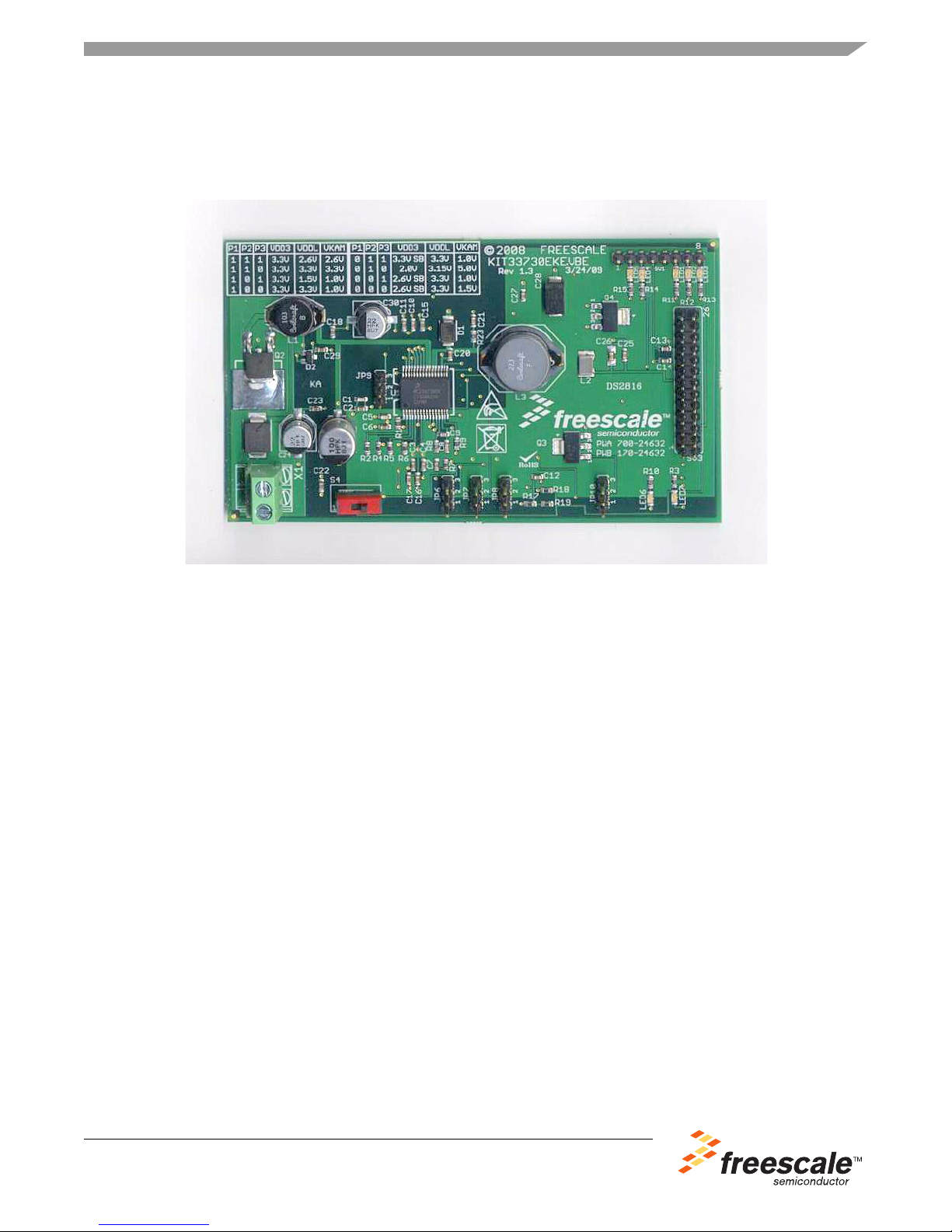
Figure 1. KIT33730EKEVBE Evaluation Board
Table of Contents
1 Kit Contents / Packing List . . . . . . . . . . . . . . . . . . . . . . . . . . . . . . . . . . . . . . . . . . . . . . . . . . . . . . . . . . . . . . . . . . . . . . 2
2 Important Notice . . . . . . . . . . . . . . . . . . . . . . . . . . . . . . . . . . . . . . . . . . . . . . . . . . . . . . . . . . . . . . . . . . . . . . . . . . . . . . 3
3 Introduction . . . . . . . . . . . . . . . . . . . . . . . . . . . . . . . . . . . . . . . . . . . . . . . . . . . . . . . . . . . . . . . . . . . . . . . . . . . . . . . . . . 4
4 Using Hardware . . . . . . . . . . . . . . . . . . . . . . . . . . . . . . . . . . . . . . . . . . . . . . . . . . . . . . . . . . . . . . . . . . . . . . . . . . . . . . 5
6 KIT33730EKEVBE Board Layout . . . . . . . . . . . . . . . . . . . . . . . . . . . . . . . . . . . . . . . . . . . . . . . . . . . . . . . . . . . . . . . . 10
7 KIT33730EKEVBE Evaluation Board Bill of Material . . . . . . . . . . . . . . . . . . . . . . . . . . . . . . . . . . . . . . . . . . . . . . . . . 12
8 References . . . . . . . . . . . . . . . . . . . . . . . . . . . . . . . . . . . . . . . . . . . . . . . . . . . . . . . . . . . . . . . . . . . . . . . . . . . . . . . . . 15
9 Revision History . . . . . . . . . . . . . . . . . . . . . . . . . . . . . . . . . . . . . . . . . . . . . . . . . . . . . . . . . . . . . . . . . . . . . . . . . . . . . 16
© Freescale Semiconductor, Inc., 2009. All rights reserved.
Page 2

Kit Contents / Packing List
1 Kit Contents / Packing List
• KIT33730EKEVBE evaluation board
• CD33730EKEVBE
2 Freescale Semiconductor
KIT33730EKEVBE Evaluation Board, Rev. 1.0
Page 3

2 Important Notice
Freescale provides the enclosed product(s) under the following conditions:
This evaluation kit is intended for use of ENGINEERING DEVELOPMENT OR EVALUATION
PURPOSES ONLY. It is provided as a sample IC pre-soldered to a printed circuit board to make it
easier to access inputs, outputs, and supply terminals. This EVB may be used with any development
system or other source of I/O signals by simply connecting it to the host MCU or computer board via
off-the-shelf cables. This EVB is not a Reference Design and is not intended to represent a final
design recommendation for any particular application. Final device in an application will be heavily
dependent on proper printed circuit board layout and heat sinking design as well as attention to
supply filtering, transient suppression, and I/O signal quality.
The goods provided may not be complete in terms of required design, marketing, and or
manufacturing related protective considerations, including product safety measures typically found
in the end product incorporating the goods. Due to the open construction of the product, it is the
user's responsibility to take any and all appropriate precautions with regard to electrostatic
discharge. In order to minimize risks associated with the customers applications, adequate design
and operating safeguards must be provided by the customer to minimize inherent or procedural
hazards. For any safety concerns, contact Freescale sales and technical support services.
Should this evaluation kit not meet the specifications indicated in the kit, it may be returned within 30
days from the date of delivery and will be replaced by a new kit.
Freescale reserves the right to make changes without further notice to any products herein.
Freescale makes no warranty, representation or guarantee regarding the suitability of its products
for any particular purpose, nor does Freescale assume any liability arising out of the application or
use of any product or circuit, and specifically disclaims any and all liability, including without limitation
consequential or incidental damages. “Typical” parameters can and do vary in different applications
and actual performance may vary over time. All operating parameters, including “Typical”, must be
validated for each customer application by customer’s technical experts.
Freescale does not convey any license under its patent rights nor the rights of others. Freescale
products are not designed, intended, or authorized for use as components in systems intended for
surgical implant into the body, or other applications intended to support or sustain life, or for any other
application in which the failure of the Freescale product could create a situation where personal
injury or death may occur.
Should Buyer purchase or use Freescale products for any such unintended or unauthorized
application, Buyer shall indemnify and hold Freescale and its officers, employees, subsidiaries,
affiliates, and distributors harmless against all claims, costs, damages, and expenses, and
reasonable attorney fees arising out of, directly or indirectly, any claim of personal injury or death
associated with such unintended or unauthorized use, even if such claim alleges that Freescale was
negligent regarding the design or manufacture of the part.Freescale™ and the Freescale logo are
trademarks of Freescale Semiconductor, Inc. All other product or service names are the property of
their respective owners. © Freescale Semiconductor, Inc. 2009
Important Notice
Freescale Semiconductor 3
KIT33730EKEVBE Evaluation Board, Rev. 1.0
Page 4

Introduction
3 Introduction
KIT33730EKEVBE Evaluation Board (EVB) is an easy-to-use circuit board used to exercise all the
functions of the MC33730 multiple output switching power supply. The EVB can be used to easily
manipulate the MC33730 functions and validate the capabilities of the IC. The board provides
connections that allow the user to supply MPCxx MCUs via hard wired connections.
3.1 EVB Features
• Provides all regulated voltages for MPC5XX MCUs and other MCUs logic and analog functions
• Adjustable frequency switching buck regulator with slew-rate control provided by jumpers
• Power sequencing provided
• Programmable voltages VDDL, VDD3 - 3% accuracy (P1, P2, and P3 jumpers)
• Programmable standby regulator VKAM - (P1, P2, and P3 jumpers) operating down to 4.5V at
KA_VBAT pin
• VDD3 can be programmed as an optional second standby regulator (P1, P2, and P3 jumpers)
• Provides two 5.0V protected supplies for sensors
• Provides reverse battery protection FET gate drive (either a diode or PFD gate drive)
• Provides necessary MCU monitoring and fail-safe support
• Pb-free packaging designated by suffix code EK
3.2 Required Equipment
Minimum required equipment: Power supply: 4.5 to 26.5V
4 Freescale Semiconductor
KIT33730EKEVBE Evaluation Board, Rev. 1.0
Page 5
4 Using Hardware
This EVB consists of a MC33730 switching power supply, power conditioning circuitry, and a set of Input
Select Jumpers. MC33730 Circuit.
4.1 LED Display
Seven LED's are provided as visual output devices for the MC33730 EVB board. A list of the LED devices
is shown below:
1. VDDH LED - Indicates when VDDH supply is operating.
2. VDDL LED - Indicates that the VDDL supply is operating.
3. VDD3 LED - Indicates that the VDD3 supply is operating.
4. VREF1 LED - Indicates that the VREF1 reference is operating.
5. VREF2 LED - Indicates that the VREF2 reference is operating.
6. IGN LED - Indicates Battery supplied to Vign.
7. IGNSW LED - Indicates that the VDD3 supply is operating.
4.2 Selection Jumper Definitions
The EVB contains four jumpers that provide certain selections for the MC33730 as follows (Bold = default
factory setting):
Using Hardware
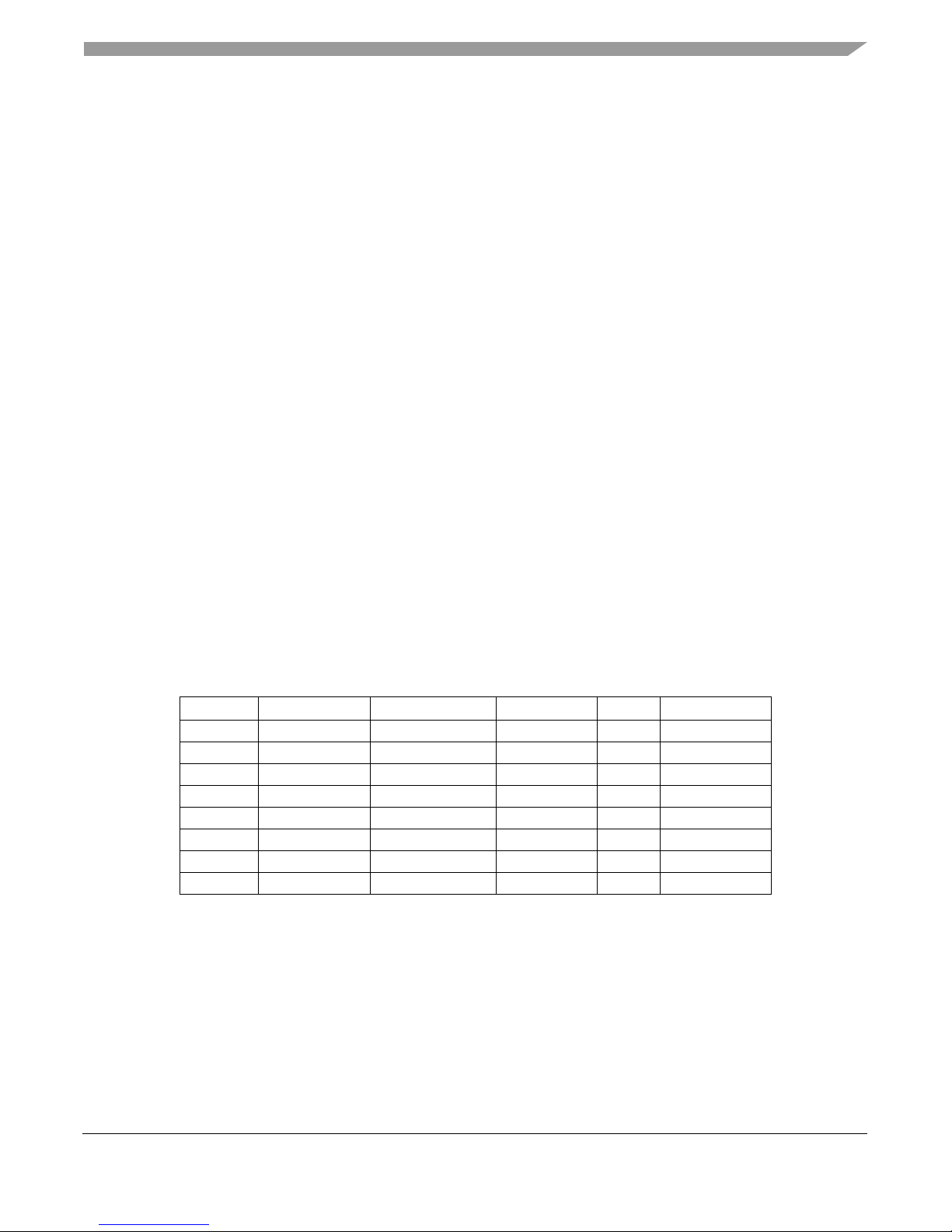
4.2.1 P1, P2, P3 Jumpers
The P1, P2, and P3 jumpers are used to determine what voltage levels will be supplied by the VDD3,
VDDL and VKAM supplies. The pins are used to hardwire the settings with the MC33730 reading the
values at startup. The table below shows the various conditions that can be set.
P1 P2 P3 VDD3 VDDL VKAM
High
High
High
High
Low
Low
Low
Low
High High 3.3V 2.6V 2.6V
High Low 3.3V 3.3V 3.3V
Low High 3.3V 1.5V 1.0V
Low Low 3.3V 3.3V 1.0V
High High 3.3V Standby 3.3V 1.0V
High Low 2.0 3.15V 5.0V
Low High 2.6V Standby 3.3V 1.0V
Low Low 2.6V Standby 3.3V 1.5V
Freescale Semiconductor 5
KIT33730EKEVBE Evaluation Board, Rev. 1.0
Page 6
Using Hardware
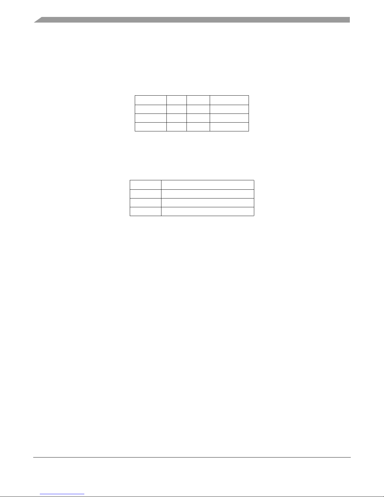
4.2.2 VDD3 Jumper
In the state where VDD3 is desired to be in standby, the VDD3 jumper is used to short the Base of the
VDD3 transistor to ground. The default case (Normal) is to leave the base connected to VDD3_B.
Jumper should be connected to Normal except for the cases where P1, P2, and P3 are as follows:
P1 P2 P3 VDD3
Low
Low
Low
4.2.3 Slew Rate (SR) Jumper
The Slew Rate Control Jumper Allows For Configurable Slew Rates For The Switching Regulator.
Connected To Boot The Slow Slew Rate Is Active And Connected To Sw The Fast Slew Rate Is Selected.
The Pin Can Be Left Open Which Results In The Medium Slew Rate Control.
SR CONDITION FOR SLEW RATE
Boot
Open
SW
High High 3.3V Standby
Low High 2.6V Standby
Low Low 2.6V Standby
Slow Slew rate
Medium Slew rate
Fast Slew rate
Setup Pins
The 33730 has multiple pins used to do initial setup for the IC. When the IC is powered up a series of
checks are done to determine the P1, P2, P3, HRT, SR and FREQ state.
The P1, P2, and P3 states are connected to jumpers to allow the user to configure the supply rails easily.
Once the IC has determined their state at startup, the status is latched into registers and changing the
jumpers does not affect the operation until the next POR or start up occurs.
The HRT pin is set to 10k. The resistor connected to HRT is R1.
The SR state is determined by the SR jumper. The slew rate of the switching regulator can be selected
to range from slow, medium and fast depending on the location (or open) of the jumper.
The FREQ pin is connected to ground via a 10kohm resistor. This pin resistance to ground determines
the frequency operation of the switching regulator. The resistor connected to FREQ is R9.
Output Supply Pins
There are multiple output power supplies integrated into the integrated circuit.
The main switching regulator, VDDH, uses a fixed frequency PWM voltage mode control. It has a 3.5A
current limit (typical) and the slew-rate is adjustable via a control pin to reduce switching noise. The
switching regulator has an adjustable frequency oscillator, which allows the user to optimize its operation
over a wide range of input voltages and component values. The VDDH regulator supplies a 5v rail and is
used as the internal power supply for VREF1 and VREF2 along with the external rail for VDD3 and VDDL.
Associated with the VDDH regulator is the INV and VCOMP pins which have been connected to optimize
the compensation for the step down regulator. A bootstrap capacitor is connected from the VSW pin to
the BOOT pin.
The linear regulators can be configured either as two normal mode regulators (VDD3, VDDL) and one
standby regulator (VKAM), or as one normal mode linear regulator (VDDL) and two standby regulators
(VKAM and VDD3 Standby). Two protected outputs, VREF1 and VREF2, are used to provide power to
external sensors.
6 Freescale Semiconductor
KIT33730EKEVBE Evaluation Board, Rev. 1.0
Page 7

Using Hardware
All of the output supplies have been brought out to two sets of connectors. The SV1 is available to monitor
the output voltages while SV3 is designed to connect to the loads or a micro motherboard.
The SV1 connector is pinned out as follows:
PIN NODE
1
2
3
4
5
6
7
8
AGND
VREF2
VREF1
VKAM
N/C
VDDH
VDDL
VDD3
The SV3 connector is pinned out as follows:
PIN NODE
1
2
3
4
5
6
7
8
9
10
11
12
13
14
15
16
17
18
19
20
21
22
23
24
25
26
Battery
Battery
VDDH
VDDH
VDD3
VDD3
VDDL
VDDL
N/C
AGND
VKAM
RST3
VDDA
RSTKAM
VREF1
RSTL
VREF2
RSTH
N/C
REGON
IGN_ON
IGN
KA
AGND
AGND
AGND
The SV3 connector also contains a number of other pin functions including the reset pins, the REGON
pin and the IGN_ON and IGN pins.
Freescale Semiconductor 7
KIT33730EKEVBE Evaluation Board, Rev. 1.0
Page 8

Using Hardware
4.2.4 MC33730 EVB Setup
To use the evaluation board the Battery connection must be made to the +12v and GND connector. Turn
on the power supply and ensure the voltage is in the normal operating range.
To apply IGN, move the slider switch to the On position (slider toward Battery connection). Ensure the
IGN_ON and IGNSW LED's are lit.
The LED's for the voltage rails will also turn on and the user can monitor the voltages and apply loads via
the connectors.
Note: The silkscreen on the PCB board is incomplete, please see Assembly Drawing on page 11 for the
complete silkscreen.
8 Freescale Semiconductor
KIT33730EKEVBE Evaluation Board, Rev. 1.0
Page 9

5 Schematic
Schematic
Figure 2. The MC33730 Schematic of the KIT33730EKEVBE Evaluation Board
Freescale Semiconductor 9
KIT33730EKEVBE Evaluation Board, Rev. 1.0
Page 10

KIT33730EKEVBE Board Layout
6 KIT33730EKEVBE Board Layout
6.1 Top Layer
Figure 3. The Top Layer of the KIT33730EKEVBE Evaluation Board
6.2 Second Layer
Figure 4. Top Layer of the KIT33730EKEVBE Evaluation Board
10 Freescale Semiconductor
KIT33730EKEVBE Evaluation Board, Rev. 1.0
Page 11

6.3 Bottom Layer
KIT33730EKEVBE Board Layout
Figure 5. The Bottom Layer of the KIT33730EKEVBE Evaluation Board
6.4 Assembly Drawing
Figure 6. The Assembly Drawing of the KIT33730EKEVBE Evaluation Board
Freescale Semiconductor 11
KIT33730EKEVBE Evaluation Board, Rev. 1.0
Page 12

KIT33730EKEVBE Evaluation Board Bill of Material
7 KIT33730EKEVBE Evaluation Board Bill of Material
Part Val ue Description Mfg. Mfg. PN Location Orientation Qty
Integrated Circuit
U1 MCZ33730 APSIC PMIC Freescale
Semiconductor
Capacitors
C1 100pF/50v CAP CERAMIC 100PF 50V 0603 SMD Panasonic ECG ECJ-1VC1H101J (1.175 1.11) R180 2
C2 100nF/50v CAP CER .10UF 50V Y5V 0603 Taiyo Yuden UMK107F104ZA-T (1.175 1.025) R180 9
C3 100nF/50v CAP CER .10UF 50V Y5V 0603 Taiyo Yuden UMK107F104ZA-T (1.625 0.52) R27
C4 10nF/50v CAP CERM .01UF 10% 50V X7R 0603 AVX
Corporation
C5 100pF/50v CAP CERAMIC 100PF 50V 0603 SMD Panasonic ECG ECJ-1VC1H101J (1.38 0.955) R180
C6 100nF/50v CAP CER .10UF 50V Y5V 0603 Taiyo Yuden UMK107F104ZA-T (1.38 0.865) R180
C7 2.7nF/16v CAP .0027UF 16V PPS FILM 0603 5% Panasonic ECG ECH-U1C272JX5 (1.825303
C8 1.5nF/16v CAP .0015UF 16V PPS FILM 0603 2% Panasonic ECG ECH-U1C152GX5 (1.921 0.685) R90 1
C9 39pF/25v CAP CER 39PF 25V NP0 0603 AVX
Corporation
C10 10nF/50v CAP CERM .01UF 10% 50V X7R 0603 AVX
Corporation
C11 4.7uF/10v CAP CER 4.7UF 10V Y5V 0603 Murata
Electronics NA
C12 10nF/50v CAP CERM .01UF 10% 50V X7R 0603 AVX
Corporation
C13 4.7uF/10v CAP CER 4.7UF 10V Y5V 0603 Murata
Electronics NA
C14 10nF/50v CAP CERM .01UF 10% 50V X7R 0603 AVX
Corporation
C15 100nF/50v CAP CER .10UF 50V Y5V 0603 Taiyo Yuden UMK107F104ZA-T (1.717295
C16 10nF/50v CAP CERM .01UF 10% 50V X7R 0603 AVX
Corporation
C17 10uF/6.3v CAP CERAMIC 10UF 6.3V X5R 0603 Panasonic ECG ECJ-1VB0J106M (1.582402
C18 100nF/50v CAP CER .10UF 50V Y5V 0603 Taiyo Yuden UMK107F104ZA-T (0.9325
C20 100nF/50v CAP CER .10UF 50V Y5V 0603 Taiyo Yuden UMK107F104ZA-T (1.955 1.51) R270
C21 390pF/50v CAP CER 390PF 50V X7R 0603 AVX
Corporation
C22 100nF/50v CAP CER .10UF 50V Y5V 0603 Taiyo Yuden UMK107F104ZA-T (0.825 0.335) R90
C23 100nF/50v CAP CER .10UF 50V Y5V 0603 Taiyo Yuden UMK107F104ZA-T (0.779299
C24 22uF/50v CAP 22UF 50V ELECT FK SMD Panasonic ECG EEV-FK1H220P (0.625 0.805) R90 2
C25 10nF/50v CAP CERM .01UF 10% 50V X7R 0603 AVX
Corporation
C26 10uF/6.3v CAP CERAMIC 10UF 6.3V X5R 0603 Panasonic ECG ECJ-1VB0J106M (3.358299
MCZ33730 (1.725 1.17) R90 1
06035C103KAT2A (1.716402
0.52)
0.521803)
06033A390JAT2A (1.89 0.795) R0 1
06035C103KAT2A (1.635201
1.776598)
GRM188F51A475
ZE20D
06035C103KAT2A (2.700598
GRM188F51A475
ZE20D
06035C103KAT2A (3.821
06035C103KAT2A (1.6 65 0.395) R27
06035C391JAT2A (2.155 1.81) R90 1
06035C103KAT2A (3.4 7 1.5) R90
(1.554406
1.776602)
0.415)
(3.82 1.555) R0
1.451299)
1.776898)
0.396402)
1.7145)
1.023402)
1.493)
R27 7
R270 1
R90
R90 2
R0
R0
R90
R270 2
R90
R0
R90
12 Freescale Semiconductor
KIT33730EKEVBE Evaluation Board, Rev. 1.0
Page 13

KIT33730EKEVBE Evaluation Board Bill of Material
Part Val ue Description Mfg. Mfg. PN Location Orientation Qty
Capacitors (Continued)
C27 10nF/50v CAP CERM .01UF 10% 50V X7R 0603 AVX
C28 100uF/10v CAPACITOR TANT 100UF 10V 20%
SMD
C29 100nF/50v CAP CER .10UF 50V Y5V 0603 Taiyo Yuden UMK107F104ZA-T (0.835 1.555) R0
C30 22uF/50v CAP 22UF 50V ELECT FK SMD Panasonic ECG EEV-FK1H220P (1.278201
C31 100uF/50v CAP 100UF 50V ELECT FK SMD Panasonic ECG EEV-FK1H101P (0.97 0.795) R90
Inductors
L1 10uH SMT POWER INDUCTOR 22 uH Coilcraft DO3316T-223MLB (0.605 1.86) R0
L2 F-bead FERRITE CHIP 120 OHMS 400MA 1812 Steward LI1812D121R-10 (3.135 1.42) R270
L3 22 uH SMT POWER INDUCTOR 10 uH Coilcraft DO5022P-103MLB (2.575 1.47) R0
Resistors
R1 10K RES 10K OHM 1/10W 5% 0603 SMD Panasonic ECG ERJ-3GEYJ103V (1.495 0.895) R90 2
R2 5.1K RES 5.1K OHM 1/10W 5% 0603 SMD Panasonic ECG ERJ-3GEYJ512V (1.225 0.67) R90 4
R3 1K RES 1.0K OHM 1/10W 5% 0603 SMD Panasonic ECG ERJ-3GEYJ102V (3.895 0.37) R270 1
R4 5.1K RES 5.1K OHM 1/10W 5% 0603 SMD Panasonic ECG ERJ-3GEYJ512V (1.325 0.67) R90
R5 5.1K RES 5.1K OHM 1/10W 5% 0603 SMD Panasonic ECG ERJ-3GEYJ512V (1.425 0.67) R90
R6 5.1K RES 5.1K OHM 1/10W 5% 0603 SMD Panasonic ECG ERJ-3GEYJ512V (1.55 0.67) R90
R7 0 RES 0.0 OHM 1/10W 5% 0603 SMD Yageo RC0603JR-070RL (1.908299
R8 25K RES 24.9K OHM 1/10W 1% 0603 SMD Panasonic ECG ERJ-3EKF2492V (1.825 0.685) R90 1
R9 10K RES 10K OHM 1/10W 5% 0603 SMD Panasonic ECG ERJ-3GEYJ103V (2.005 0.71) R90
R10 470 RES 470 OHM 1/10W .1% 0603 SMD Panasonic ECG ERA-3AEB471V (3.686598
R11 470 RES 470 OHM 1/10W .1% 0603 SMD Panasonic ECG ERA-3AEB471V (3.929398
R12 470 RES 470 OHM 1/10W .1% 0603 SMD Panasonic ECG ERA-3AEB471V (4.032799
R13 470 RES 470 OHM 1/10W .1% 0603 SMD Panasonic ECG ERA-3AEB471V (4.132197
R14 470 RES 470 OHM 1/10W .1% 0603 SMD Panasonic ECG ERA-3AEB471V (3.628902
R15 470 RES 470 OHM 1/10W .1% 0603 SMD Panasonic ECG ERA-3AEB471V (3.524402
R17 4.7K RES 4.7K OHM 1/10W 5% 0603 SMD Panasonic ECG ERJ-3GEYJ472V (2.635 0.17) R0 3
R18 4.7K RES 4.7K OHM 1/10W 5% 0603 SMD Panasonic ECG ERJ-3GEYJ472V (2.78 0.295) R0
R19 4.7K RES 4.7K OHM 1/10W 5% 0603 SMD Panasonic ECG ERJ-3GEYJ472V (2.785 0.17) R180
R23 1 RESISTOR 1.0 OHM 1/10W 5% 0603 Panasonic ECG ERJ-3GEYJ1R0V (2.155 1.67) R270 1
Corporation
Kemet T525D107M010AT
06035C103KAT2A (2.5 9 2.035) R90
(2.87 2.025) R270 1
E025
R0
1.8235)
R90 1
0.521398)
R270 6
0.363201)
R90
2.085)
R90
2.0845)
R90
2.081102)
R90
2.083299)
R90
2.085799)
Freescale Semiconductor 13
KIT33730EKEVBE Evaluation Board, Rev. 1.0
Page 14

KIT33730EKEVBE Evaluation Board Bill of Material
Part Val ue Description Mfg. Mfg. PN Location Orientation Qty
Headers & Jumpers
SV1 ---- CONN HEADER VERT .100 8POS 15AU Tyco Electronics 87224-8 (3.775 2.37) R0 1
SV3 ---- CONN HDR BRKWAY .100 26POS
VERT
JP6 CONN HEADER VERT .100 2POS 15AU Tyco Electronics 87224-2 (1.925 0.27) R90 5
JP7 CONN HEADER VERT .100 2POS 15AU Tyco Electronics 87224-2 (2.175 0.27) R90
JP8 CONN HEADER VERT .100 2POS 15AU Tyco Electronics 87224-2 (2.425 0.27) R90
JP9 CONN HEADER VERT .100 2POS 15AU Tyco Electronics 87224-2 (1.346701
JP10 CONN HEADER VERT .100 2POS 15AU Tyco Electronics 87224-2 (3.275 0.27) R90
Connectors
X1 AK300/2 CONN TERM BLOCK 2POS 5.08MM
PCB
Switch
S4 ---- SW TOGGLE SPDT .221" ACT PC .4VA Tyco Electronics TT11DGPC104 (1.125 0.22) R0
Diodes
D1 SMB DIODE TVS 40V 600W UNIDIR 5% SMB Little Fuse SMBJ40A (1.94 1.72) R90 1
D2 SOT23 DIODE ULTRAFAST HI COND SOT-23 Fairchild
D 4 M U R S 3 2 0T3DIODE ULTRA FAST 3A 200V SMC ON
LED1 Green LED LED PURE GREEN S-J TYPE 0805 Panasonic LNJ306G5PRX (3.924701
LED2 Green LED LED PURE GREEN S-J TYPE 0805 Panasonic LNJ306G5PRX (4.027799
LED3 Green LED LED PURE GREEN S-J TYPE 0805 Panasonic LNJ306G5PRX (4.13 2.22) R180
LED4 Green LED LED PURE GREEN S-J TYPE 0805 Panasonic LNJ306G5PRX (3.628201
LED5 Green LED LED PURE GREEN S-J TYPE 0805 Panasonic LNJ306G5PRX (3.522701
LED6 Green LED LED PURE GREEN S-J TYPE 0805 Panasonic LNJ306G5PRX (3.686799
LED7 Green LED LED PURE GREEN S-J TYPE 0805 Panasonic LNJ306G5PRX (3.897
Transistors
Q2 IRFR5305 MOSFET P-CH 55V 31A D PAK International
Q3 BCP68T1 TRANS NPN AUDIO 1A 25V SOT223 ON
Q4 BCP68T1 TRANS NPN AUDIO 1A 25V SOT223 ON
Freescale does not assume liability, endorse, or warrant components from external manufacturers that are referenced in circuit drawings or
tables. While Freescale offers component recommendations in this configuration, it is the customer’s responsibility to validate their application
Tyco Electronics 9-146261-0-13 (4.025 1.27) R90 1
R90
1.213398)
Phoenix Contact 1729128 (0.325 0.32) R270 1
BAV74 (0.725 1.49) R270 1
Semiconductor
MURS320T3G (0.265 0.785) R270 1
Semiconductor
R180 7
2.223602)
R180
2.223398)
R180
2.220406)
R180
2.223602)
R180
0.2185)
R180
0.228398)
IRFR5305TRPBF (0.285 1.295) R180 1
Rectifier
BCP68T1G (2.905 0.685) R90 2
Semiconductor
BCP68T1G (3.45 1.845) R270
Semiconductor
14 Freescale Semiconductor
KIT33730EKEVBE Evaluation Board, Rev. 1.0
Page 15

8 References
Following are URLs where you can obtain information on other Freescale products and application
solutions:
Description URL
Data Sheet www.freescale.com/files/analog/doc/data_sheet/MC33730.pdf
Freescale’s Web Site www.freescale.com
Freescale’s Analog Web Site www.freescale.com/analog
Freescale’s Power Management Web Site www.freescale.com/powermanagement
Freescale’s Automotive Applications Web Site www.freescale.com/automotive
References
Freescale Semiconductor 15
KIT33730EKEVBE Evaluation Board, Rev. 1.0
Page 16

Revision History
9 Revision History
REVISION DATE DESCRIPTION OF CHANGES
1.0
9/2009 • Initial Release
16 Freescale Semiconductor
KIT33730EKEVBE Evaluation Board, Rev. 1.0
Page 17

How to Reach Us:
Home Page:
www.freescale.com
Web Support:
http://www.freescale.com/support
USA/Europe or Locations Not Listed:
Freescale Semiconductor, Inc.
Technical Information Center, EL516
2100 East Elliot Road
Tempe, Arizona 85284
1-800-521-6274 or +1-480-768-2130
www.freescale.com/support
Europe, Middle East, and Africa:
Freescale Halbleiter Deutschland GmbH
Technical Information Center
Schatzbogen 7
81829 Muenchen, Germany
+44 1296 380 456 (English)
+46 8 52200080 (English)
+49 89 92103 559 (German)
+33 1 69 35 48 48 (French)
www.freescale.com/support
Japan:
Freescale Semiconductor Japan Ltd.
Headquarters
ARCO Tower 15F
1-8-1, Shimo-Meguro, Meguro-ku,
Tokyo 153-0064
Japan
0120 191014 or +81 3 5437 9125
support.japan@freescale.com
Asia/Pacific:
Freescale Semiconductor China Ltd.
Exchange Building 23F
No. 118 Jianguo Road
Chaoyang District
Beijing 100022
China
+86 10 5879 8000
support.asia@freescale.com
For Literature Requests Only:
Freescale Semiconductor Literature Distribution Center
P.O. Box 5405
Denver, Colorado 80217
1-800-441-2447 or +1-303-675-2140
Fax: +1-303-675-2150
LDCForFreescaleSemiconductor@hibbertgroup.com
Information in this document is provided solely to enable system and
software implementers to use Freescale Semiconductor products. There are
no express or implied copyright licenses granted hereunder to design or
fabricate any integrated circuits or integrated circuits based on the
information in this document.
Freescale Semiconductor reserves the right to make changes without further
notice to any products herein. Freescale Semiconductor makes no warranty,
representation or guarantee regarding the suitability of its products for any
particular purpose, nor does Freescale Semiconductor assume any liability
arising out of the application or use of any product or circuit, and specifically
disclaims any and all liability, including without limitation consequential or
incidental damages. “Typical” parameters that may be provided in Freescale
Semiconductor data sheets and/or specifications can and do vary in different
applications and actual performance may vary over time. All operating
parameters, including “Typicals”, must be validated for each customer
application by customer’s technical experts. Freescale Semiconductor does
not convey any license under its patent rights nor the rights of others.
Freescale Semiconductor products are not designed, intended, or authorized
for use as components in systems intended for surgical implant into the body,
or other applications intended to support or sustain life, or for any other
application in which the failure of the Freescale Semiconductor product could
create a situation where personal injury or death may occur. Should Buyer
purchase or use Freescale Semiconductor products for any such unintended
or unauthorized application, Buyer shall indemnify and hold Freescale
Semiconductor and its officers, employees, subsidiaries, affiliates, and
distributors harmless against all claims, costs, damages, and expenses, and
reasonable attorney fees arising out of, directly or indirectly, any claim of
personal injury or death associated with such unintended or unauthorized
use, even if such claim alleges that Freescale Semiconductor was negligent
regarding the design or manufacture of the part.
Freescale™ and the Freescale logo are trademarks of
Freescale Semiconductor, Inc. All other product or service names
are the property of their respective owners.
© Freescale Semiconductor, Inc. 2009. All rights reserved.
KT33730UG
Rev. 1.0
9/2009
 Loading...