

Page 1

i.MX27 PDK 1.0 Hardware
User's Guide
Document Number: 924-76325
Rev. 1.0
11/2008
Page 2

How to Reach Us:
Home Page:
www.freescale.com
Web Support:
http://www.freescale.com/support
USA/Europe or Locations Not Listed:
Freescale Semiconductor
Technical Information Center, EL516
2100 East Elliot Road
Tempe, Arizona 85284
+1-800-521-6274 or +1-480-768-2130
www.freescale.com/support
Europe, Middle East, and Africa:
Freescale Halbleiter Deutschland GmbH
Technical Information Center
Schatzbogen 7
81829 Muenchen, Germany
+44 1296 380 456 (English)
+46 8 52200080 (English)
+49 89 92103 559 (German)
+33 1 69 35 48 48 (French)
www.freescale.com/support
Japan:
Freescale Semiconductor Japan Ltd.
Headquarte rs
ARCO Tower 15F
1-8-1, Shimo-Meguro, Meguro-ku,
Tokyo 153-0064, Japan
0120 191014 or +81 3 5437 9125
support.japan@freescale.com
Asia/Pacific:
Freescale Semiconductor China Ltd.
Exchange Building 23F
No. 118 Jianguo Roa d
Chaoyang District
Beijing 100022
China
+86 010 5879 8000
support.asia@freescale.com
For Literature Requests Only:
Freescale Semiconductor Literature Distribution Center
P.O. Box 5405
Denver, Colorado 80217
1-800-441-2447 or 303-675-2140
Fax: 303-675-2150
LDCForFreescaleSemiconductor@hibbertgroup.com
Information in this document is provided solely to enable system and software
implementers to use Freescale Semiconductor products. There are no express or
implied copyright licenses granted hereunder to design or fabricate any integrated
circuits or integrated circuits based on the information in this document.
Freescale Semiconductor reserves the right to make changes without further notice to
any products herein. Freescale Semiconductor makes no warranty, representation or
guarantee regarding the suitability of its products for any particular purpose, nor does
Freescale Semiconductor assume any liability arising out of the application or use of
any product or circuit, and specifically disclaims any and all liability, including without
limitation consequential or incidental damages. “Typical” parameters that may be
provided in Freescale Semiconductor data sheets and/or specifications can and do
vary in different applications and actual performance may vary over time. All operating
parameters, including “Typicals”, must be validated for each customer application by
customer’s technical experts. Freescale Semiconductor does not convey any license
under its patent rights nor the rights of others. Freescale Semiconductor products are
not designed, intended, or authorized for use as components in systems intended for
surgical implant into the body, or other applications intended to support or sustain life,
or for any other application in which the failure of the Freescale Semiconductor product
could create a situation where personal injury or death may occur. Should Buyer
purchase or use Freescale Semiconductor products for any such unintended or
unauthorized application, Buyer shall indemnify and hold Freescale Semiconductor and
its officers, employees, subsidiaries, affiliates, and distributors harmless against all
claims, costs, damages, and expenses, and reasonable attorney fees arising out of,
directly or indirectly, any claim of personal injury or death associated with such
unintended or unauthorized use, even if such claim alleges that Freescale
Semiconductor was negligent regarding the design or manufacture of the part.
Freescale™ and the Freescale logo are trademarks of Freescale Semiconductor, Inc.
All other product or service names are the property of their respective owners.
© Freescale Semiconductor, Inc. 2007. All rights reserved.
Page 3

About This Book .....................................................................................................v
Audience............................................................................................................................... v
Organization.......................................................................................................................... v
Conventions.......................................................................................................................... vi
Definitions, Acronyms, and Abbreviations.............................................................................vi
Chapter 1 Introduction ....................................................................................... 1-1
1.1 i.MX27 3-Stack Features....................................................................................... 1-2
1.2 i.MX27 3-Stack Components................................................................................. 1-3
1.3 System and User Requirements.............................................................................. 1-4
1.4 3-Stack System Operating Specifications................................................................ 1-4
Chapter 2 Configuration and Connections........................................................... 2-1
2.1 Debug Board Configuration................................................................................... 2-1
2.1.1 Debug Board Top Switches and Connectors........................................................... 2-1
2.1.2 Debug Board Bottom Connectors .......................................................................... 2-3
2.2 Personality Board Connectors................................................................................ 2-4
2.2.1 Personality Board Top Connectors......................................................................... 2-4
2.2.2 Personality Board Bottom Connectors.................................................................... 2-5
2.3 CPU Board Connector........................................................................................... 2-6
2.4 Setting the Debug Switches.................................................................................... 2-7
Chapter 3 Build the Platform .............................................................................. 3-1
3.1 Build a Development Platform: Assemble 3 Boards................................................ 3-2
3.1.1 Connect Personality Board to Debug Board........................................................... 3-2
3.1.2 Connect CPU Board to Debug Board..................................................................... 3-3
3.1.3 Connect Development Platform to PC; Run Preloaded Image................................. 3-4
3.2 Build a Demo Platform: Assemble 2 Boards........................................................... 3-5
3.2.1 Connect CPU Board to Personality Board.............................................................. 3-6
3.2.2 Connect Power Supply; Run Pre-loaded Demo....................................................... 3-7
Freescale Semiconductor i.MX27 PDK 1.0 Hardware User's Guide, Rev. 1.0 iii
Page 4

Chapter 4 Functional Operation.......................................................................... 4-1
4.1 Functional Block Diagrams.................................................................................... 4-1
4.2 3-Stack Memory Map............................................................................................ 4-3
4.3 CPLD on the Debug Board.................................................................................... 4-4
4.3.1 CPLD Features ...................................................................................................... 4-4
4.3.2 CPLD Memory Map.............................................................................................. 4-4
4.3 .3 Pro grammin g the CPLD ......................................................................................... 4-5
4.4 i.MX27 GPIO Grouping......................................................................................... 4-7
Chapter 5 Connectors and Signals....................................................................... 5-1
5.1 500 Pins Board to Board Co nnector....................................................................... 5-2
5.2 TV/Headphone Jack..............................................................................................5-16
5.3 LCD Connector ....................................................................................................5-18
5.4 Keypad .................................................................................................................5-20
5.5 Current Measurement Connector...........................................................................5-21
5.6 Battery Operation..................................................................................................5-21
i.MX27 PDK 1.0 Hardware User's Guide, Rev. 1.0 Freescale Semiconductor
iv
Page 5

About This Book
This document explains how to connect and operate the i.MX27 3-Stack Platform System.
Audience
This document is intended for software, hardware, and system engineers who are planning to use
the i.MX27 hardware and for anyone who wants to understand more about the i.MX27 hardware.
Organization
This document contains the following chapters.
Chapter 1 Intr oduces the features and functionality of the 3-Stack board.
Chapter 2 Provides configuration and setup information.
Chapter 3 Explains how to assemble the boards.
Chapter 4 Provides block diagrams and memory mapping.
Chapter 5 Provides connector pin assignments and signal descriptions.
Freescale Semiconductor i.MX27 PDK 1.0 Hardware User's Guide, Rev. 1.0
v
Page 6

Conventions
This docu ment us e s the following conventions :
Courier Is used to identify comman ds, explicit comman d p ar ame ter s, code
examples, expressions, data types, and directives.
Italic Is used for emphasis, to identify new terms, and for replaceable command
parameters.
Definitions, Acronyms, and Abbreviations
Th e followin g lis t defines the abb re viations used in th is document.
APMS Atlas Power Management System
ATA Har d dr ive interface spec
CD Compact Disk
CM OS Comp leme ntary Meta l Oxide Se miconductor
CPLD Custom Progr ammed Logic Devices
CPU Central Processing Unit
CSI Camera Sensor Imaging
CSPI Serial Peripheral Interface
DCE Data Communication s E quipment
DDR Double Data Rate
DIP Dual In-line Package
DMA Direct Memory Access
DTE Data Terminal Equipment
DUART Dual Universal Asynchronous Receiver/Transmitter
EEPROM Electrically Erasable Progr ammable Read Only Memory
EPROM Erasable Programmable Read Only Memory
FIR Infra Red
GPIO General Purpose Input/Output
GPO General Purpose Output
I
2C Inter-Integrated Circuit
ICE In-Circuit Emulator
I/O I nput/Output
IrDA Infrared Data Association
ISA Instr umentation, System, and Automation Society
JTAG Joint Test Access Group
LAN Local Area Network
LCD Liquid Crystal Display
LED Light Emitting Diode
MB Mega byte
MCU Microcontroller Unit
MM C Multi- med ia Card
MC P M ulti-ch ip p roduct
i.MX27 PDK 1.0 Hardware User's Guide, Rev. 1.0 Freescale Semiconductor
vi
Page 7

MS Memory St ick
NVRA M Non -volatile Ra n dom Access Memory
OTG On t he Go
PC Personal Computer
PCMCIA Personal Computer Memory Card International Asso ciation
PCB Printed Circuit Board
PHY Physical interface
POR Power on Reset
PSRAM Pseudo Random Access Memo ry
PWM Pulse Width Modulation
QVGA Graphics Adapter
RAM Random Access Memory
SD SanDisk (Smart Media)
SDRAM Synchronous Dynamic Random Access Memory
SI System International (international syst em of units and measures)
SIMM Single In-Line Memory Module
SPST Single Pole Single Throw
SSI2 Synchro nous Serial Interface
TFT Th in Film Tr ansistor
UART Universal Asynchrono us Receiver/Transmitter
USB Univer sal Serial Bus
Freescale Semiconductor i.MX27 PDK 1.0 Hardware User's Guide, Rev. 1.0
vii
Page 8
Chapter 1
Introduction
The i.MX27 3-Stack Platform System helps you develop new solutions using the i.MX27
ARM9™ MCU and the MC13783 audio and power management chip.
The 3-Stack platform comprises the CPU Engine board, Personality board, and Debug board. The
system suppo r ts application software development, target bo ar d debugging, and optional circuit
cards. The CPU board can be run in stand-alone mode for code development. An LCD display
panel is supplied with the 3-Stack system.
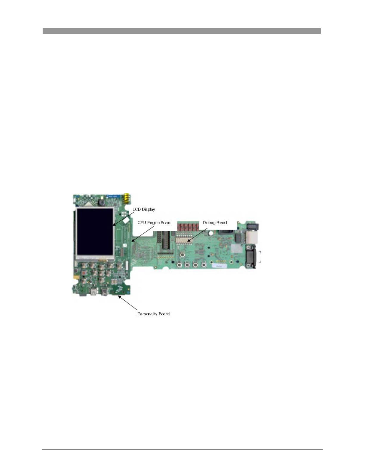
Figure 1-1 shows the major components of the 3-Stack system.
Figure 1-1 Major Components of the 3-Stack System
Freescale Semiconductor i.MX27 PDK 1.0 Hardware User's Guide, Rev. 1.0 1-1
Page 9
1.1 i.MX27 3-Stack Features
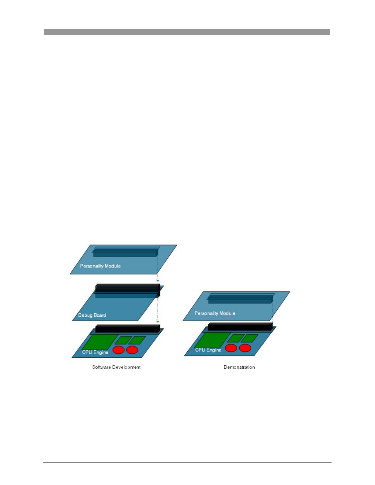
The 3-Stack system can be used in two ways: the development mode requires a three-board
as sembly; the d emons tratio n mode r eq uires only a two-board assembly (without th e Debug
board).
The system includes the following features
.
• Near form-factor demonstration modules and working platforms.
• Solid reference schematics that closely resemble final products to aid customers’ designs.
• Three-board system, which includes:
⎯ CPU board with i.MX27 ARM9 MCU, MC13783 chip
⎯ Personality boar d with peripheral components and interface connectors
⎯ Debug board with two RS-232 interfaces, 10/100 Base-T Ethernet connector, and
current measure connectors.
• Utilizes reliable high-density connector to interface between boards.
Fig ure 1- 2 illu str ates the three-board assembly (left) fo r dev elop ment and th e tw o-boar d a ssembly
(right) for demonstration.
Figure 1-2 Board Assemblies
i.MX27 PDK 1.0 Hardware User's Guide, Rev. 1.0 Freescale Semiconductor
1-2
Page 10

1.2 i.MX27 3-Stack Components
The 3-Stack board set includes the following co mponents:
• +5.0 VDC, 2.4 A universal power supply
• +4.2 V 2400mAh battery power supply and battery charging function
• 2.8- inch th in film transistor liq uid crystal display ( TF TL CD ) pan el w ith touc h panel an d
LED backlight
• 2.4-inch Quarter Video Graphics Arr ay (QVGA) smart display panel connector
• Image sensor camera connector
• Con figurable inte llige nt man ag ement of sys tem p ower through pow er man ag ement ch ip
MC13783
• Two selectable syst em clock sources, 32.768KHz and 26MHz
• 256 MB of NAND Flash Memory
• 128 MB of 32-bit DDR SDRAM memory
• RealView- I CE® debug support`
• Pushbutton reset (o n CPU) o r reset control from MC13783
• Ster eo micr ophone jack, headphone and video jack, ster eo and mono (ear piece) speaker
t ermina ls
• One connector to outboard GPS module
• FM receiver
• TV decoder that supports 8-bit color, and NTSC and PAL formats
• SD card co nnecto r s, with card sense functionality
• Onboard keypad and keypad co nnecto r
• Onboard Wi-Fi CERTIFIED™ IEEE 802.11™ b/g standards and Bluetooth(r) Core
Specification Version 2.0 + EDR (enhanced data rate) co mbination module
• One USB high- speed host transceiver, with standard USB host connector
• ATA5-compliant co nt rolle r wit h one 44-position du al ro w, 2mm h eade r for small fo rm-
factor disk driver s, and one 40-pin ZIF connector for Toshiba HDD
• Onboard accelerometer with sensit ivity in three separat e axes (X, Y, and Z)
• Two RS- 232 interfaces with DB-9 connectors: one is driven by UART channel internal to
the i.MX27 and supports DCE with optional full modem controls; the other is DTE with
o ptiona l full mod em con trols
Freescale Semiconductor i.MX27 PDK 1.0 Hardware User's Guide, Rev. 1.0
1-3
Page 11
1.3 System and User Requirements
You will n ee d a n IBM® PC or comp atible computer that in clu de s:
• Windows 98™, ME™, 2000™, XP™, or NT ™ (version 4.0) operating system
• One +5VDC, 2.4A power supply with a female (inside posit ive) power co nnecto r
(included)
CAUTION
Never supply more than +5.5 V power to the i.MX27 3-Stack.
Doing so can dama ge b oar d c omponents.
1.4 3-Stack System Operating Specifications
Table 1-1 identifies the clock, environmental conditions, and dimensions of the i. MX27 3-S tack
system.
Table 1-1 Specifications
Characteristic Specifications
Clock Selectable 32.768KHz or 26 MHz
Temperature:
Operating
Storage
Relative Humidity 0 to 90% (noncondensing)
Power Requirements 4.5V to 5.5 V DC @1.5A
Dimensions
-10 °C to + 50 °C
-40 °C to +85 °C
CPU Engine board: 38.989mm x 69.012mm
Personality board: 71.428mm x 129.462mm
Debug board: 71.400mm x 174.900mm
i.MX27 PDK 1.0 Hardware User's Guide, Rev. 1.0 Freescale Semiconductor
1-4
Page 12
Chapter 2
Configuration and Connections
This section contains configuration information, connection descriptions, and other operational information
that may be useful during the development process.
2.1 Debug Board Configuration
Th e D ebug bo ard pro vides an easy, familia r inter face for pr ogramming and debugging the i.MX
development systems and reference platforms.
This section describes the switches and connectors o n t he t op of the Debug board, and the connector to t he
CPU Engine bo ar d on the bott om of the Debug board. The Debug board is a small card that you can insert
o r remov e fr om th e p latfor m. The ab ility to remov e the debug bo ard is a major ad van tage to marketing a nd
sa les tea ms who want to d emonst rate and sh owcase a varie ty of pro ducts an d id ea s in a streamlined, nea r
form factor way, without t he added software development bulk.
2.1.1 Debug Board Top Switches and Connectors
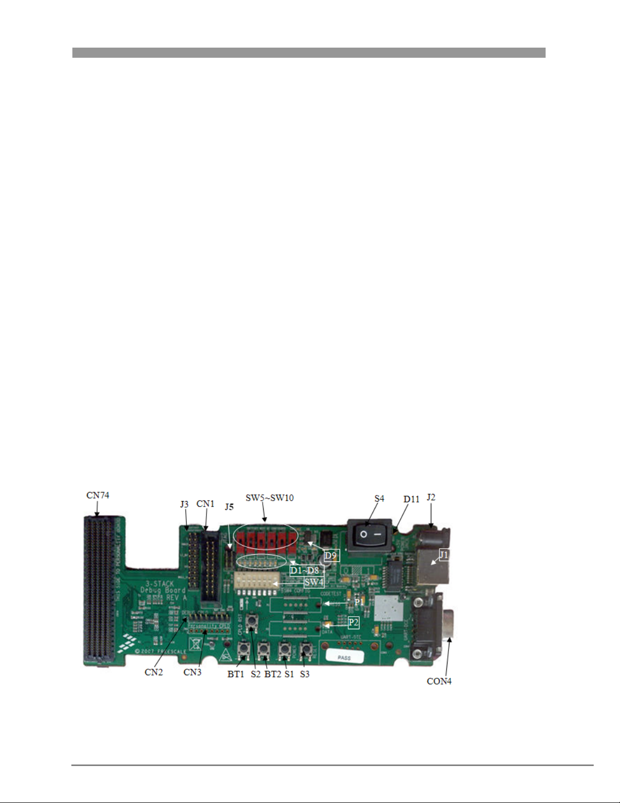
Figure 2-1 ident ifies the switches and connectors located o n top of the Debug board. Table 2-1 describes
the switches and connectors.
.
Freescale Semiconductor i.MX27 PDK 1.0 Hardware User's Guide, Rev. 1.0 2-1
Figure 2-1 Debug Board, Top View
Page 13
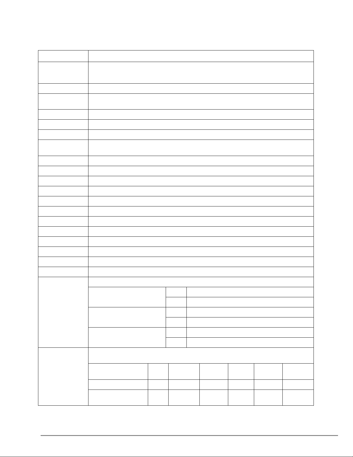
Table 2-1 Debug Board, Top Components
Component Description
S1 Power button, connected to the ON1B input of the MC13783 through the 500 pin connector.
The line is pulled up, and pushing it grounds the line. If MC13783 is in Off, User Off or
Memory Hold Mode, the board can be powered on by pushing the button
S2 Reset button, which resets the Debug board
S3 System reset switch, connected to the RESETB to MX27. The line is pulled up, and pushing it
grounds the line.
S4 Power on switch, which powers up the Debug board when set to 1.
J1 10/100 Base T Ethernet RJ45 Connector
J2 5.0V DC power connector
J3 Current measure connector; measures the current at various points of CPU Engine and
Personality board from the connector
F1 Re-settable fuse; re-settable over-current protection
D1 – D8 LEDs for CPLD debug
D9 LED for debug board 3.3V power; the LED will be bright when debug 3.3V is power on
D11 LED for DC power supply; the LED will be bright when 5.0V DC power is supplied
P1 WEIM Address measure connector; can support CodeTest Interface Probe
P2 WEIM Data measure connector; can support CodeTest Interface Probe
BT1, BT2 Test buttons for CPLD
CN1 i.MX27 JTAG connector
CN2 Debug board CPLD JTAG connector
CN3 Personality board CPLD JTAG connector (Reserved)
CN74 500 pins connector to Personality board
CON4 UART (DCE) DB9 female connector
SW4
SW5 – SW10
Enable switch; the switch designation settings follow.
ON Serial port UART (DTE) CON3 is selected SW4-1 UART Port Select
OFF Serial port UART (DCE) CON4 is selected
ON Enable NorFlash on Debug board SW4-2 NorFlash Enable
OFF Disable Norflash on Debug board
SW4-8 Power Enable
Boot mode setting switches; SW5 to SW10 settings determine where the processor begins
program execution; the valid combinations of the switch settings follow.
ON Power supply to three boards
OFF Power supply to Debug board only
Boot mode device SW5 Boot4
SW6
UART/USB Bootloader X 0 0 0 0 0
8-bit NAND Flash
(2KB page) Ext
i.MX27 PDK 1.0 Hardware User's Guide, Rev. 1.0 Freescale Semiconductor
2-2
X 0 0 0 1 0
Boot3
SW7
Boot2
SW8
Boot1
SW9
Boot0
SW10
Page 14
2.1.2 Debug Board Bottom Connectors
Fig ure 2- 2 illu str ates the bottom vie w of the Debug b oar d, wh ere J4 identifies t he 500-pin connector t o the
CPU Engine boar d.
Figure 2-2 Debug Board Bottom View
Freescale Semiconductor i.MX27 PDK 1.0 Hardware User's Guide, Rev. 1.0
2-3
Page 15

2.2 Personality Board Connectors
This section describes the switches and connectors o n t he t op of the Personality board, and the connecto r s
on the bottom of the Personality board.
2.2.1 Personality Board Top Connectors
Figure 2-3 ident ifies the connectors on the top of the Personalit y Board.
Figure 2-3 Personality Board Connectors, Top View
Table 2-2 Personality Board Connectors, Top View
Component
Identifier
E1 Wi-Fi antenna
E2 Bluetooth antenna
F1 Resettable over current-protection fuse
J10 Mini USB OTG High speed connector, for USB OTG connection
Description
J14 Epson VGA LCD connector
J15 Giantplus QVGA Smart display connector
i.MX27 PDK 1.0 Hardware User's Guide, Rev. 1.0 Freescale Semiconductor
2-4
Page 16
Component
Identifier
Mini USBOTG High speed connector, for USB HOST connection. NOTE: J18 mini USBOTG
J18
J19 Audio and Video connector
CN13 GPS module connector
CN14 2.0M pixel CMOS sensor connector
CN16 Debug port for Wi-Fi and Bluetooth module
CN70 40 pin ZIF connector for Toshiba HDD
S7 – S17 Onboard keypad
High speed connector, for USB HOST connection.
Note: This connector is not used with the i.MX27 PDK; it is used only with the i.MX31 PDK.
Description
2.2.2 Personality Board Bottom Connectors
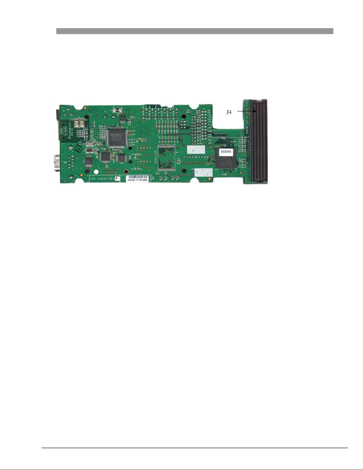
Fig ure 2-4 illustra tes the b ottom v iew of th e Personality b oar d. T able 2-3 describe s the connectors.
Figure 2-4 Personality Board, Bottom View
Freescale Semiconductor i.MX27 PDK 1.0 Hardware User's Guide, Rev. 1.0
2-5
Page 17

Table 2-3 Personality Board Bottom Connectors
Component
Identifier
B1 Coin cell battery
J12 5.0 Vdc power connector
J16 10/100BT Fast Ethernet Connector
CN12 44-position dual row, 2mm header for HDD
CN31 SD card socket
CN73 500-pin Connector to CPU Engine board (In Demo Mode) or Debug board (In Debug Mode)
CN15 Battery Connector
Description
2.3 CPU Board Connector
Fig ure 2- 5 illustrates th e bottom view of the CPU Engine b oard, w here J1 is the 500-pin connector to the
Personality board (for demonstrations) or the Debug board (for software development).
J1
Figure 2-5 CPU Engine Board, Bottom View
i.MX27 PDK 1.0 Hardware User's Guide, Rev. 1.0 Freescale Semiconductor
2-6
Page 18

2.4 Setting the Debug Switches
To set the Debug board switches, use these steps:
1. Set CPU Engine and Perso nality bo ar d power enable switch SW4- 8.
2. Set Boot Mo de Switches, SW9, SW10.
Freescale Semiconductor i.MX27 PDK 1.0 Hardware User's Guide, Rev. 1.0
2-7
Page 19

Chapter 3
Build the Platform
This chapter explains how to connect the t hree types of 3-Stack boards (Debug, Personality, CPU) together
(Figure 3-1), to make either a development platform (Personality board + CPU board + Debug board), or a
demonstration platform (Personality board + CPU board); and how to connect the 3-Stack platform to your
PC.
Figure 3-1 Platform Configurations
The three 3-Stack boar ds in your development kit may already be assembled. I f the three boar ds are already
assembled, review the procedures in the following sections, and be sure to configure the Debug board
appropriately.
• To build a development platform, follow the procedures in “Build a Development Platform:
Assemble 3 Boards” on page 3-2.
• T o b uild a d emons tra tion pla tform, fo llow the procedur es in “Build a D emo Platfor m: Asse mble 2
Boards” on page 3-5.
Freescale Semiconductor i.MX27 PDK 1.0 Hardware User's Guide, Rev. 1.0 3-1
Page 20

3.1 Build a Development Platform: Assemble 3 Boards
This section explains ho w to co nnect t he Personalit y, Debug, and CPU boards.
3.1.1 Connect Personality Board to Debug Board
The Personality board connects to t he Debug board using a 500-pin connector. The connector is keyed to
avoid misconnection, so t here is only one way to connect these boards. Connect the Personality board to
the Debug board. See Figure 3-2.
Figure 3-2 Install Personality Board onto Debug Board
i.MX27 PDK 1.0 Hardware User's Guide, Rev. 1.0 Freescale Semiconductor
3-2
Page 21

3.1.2 Connect CPU Board to Debug Board
After connecting the Personality bo ar d to t he Debug board, now connect the CPU board to the underside
of the Debug board (See Figure 3-3).
Figure 3-3 Align CPU Board and Debug/Personality Board
Freescale Semiconductor i.MX27 PDK 1.0 Hardware User's Guide, Rev. 1.0
3-3
Page 22

3.1.3 Connect Development Platform to PC; Run Preloaded Image
Fig ure 3- 4 illustrates th e switc h es and PC c on nection.
Figure 3-4 Connecting the Platform to Your PC
To co nnect t he 3-Stack platform to your host PC, use t hese steps:
1. Connect one end of an RS-232 serial cable (included in the kit) to a serial port connecto r ( CON4)
on the Debug board and connect the ot her end to a COM port on the host PC.
⎯ Configure SW4-1 t o ON.
⎯ Make sure that SW4-8 is ON, to supply power to all three boards.
⎯ Configure SW4-2 to OFF.
2. Confirm that the Bootstrap switches (SW5–SW10) are set for NAND boot; see the following table.
Boot Mode
Device
UART/USB
Bootloader
SW5 SW6
(Boot4)
X 0 0 0 0 0
SW7
(Boot3
SW8 SW9 SW10
8-bit NAND
Flash (2KB
page) Ext
X 0 0 0 1 0
i.MX27 PDK 1.0 Hardware User's Guide, Rev. 1.0 Freescale Semiconductor
3-4
Page 23

3. Connect the regulated 5V power supply to t he appro pr iate po wer adapter. Plug the power adapt er
into an electrical ou tlet and the 5V line connector into the J2 (5V POWER JACK) connector on the
Debug board. See Figure 3-5.
4. Start a ser ial console application on your host PC with the following configuration:
⎯ Baud rate: 115200
⎯ Data Bits: 8
⎯ Parity: none
⎯ Stop Bits: 1
⎯ Flow Control: none
5. On the Debug board, switch the power switch (S4) to 1.
6. The O S ima ge pre-loade d in the 3 -Stack board will boot a nd th e debug message s fr om th e
bootloader should now appear o n the serial console application on your PC
3.2 Build a Demo Platform: Assemble 2 Boards
This section explains how to make a demonstration platform using the Personality and CPU boar ds. T o
make a demo nst r ation platform, the CPU board is directly co nnected t o the Personality board using the
500-pin connector; the Debug board is not used (Figure 3-5).
NOTE
If your system is already configured as a development platform (using all three
boards), disconnect all b oards fr om eac h other.
Freescale Semiconductor i.MX27 PDK 1.0 Hardware User's Guide, Rev. 1.0
3-5
Page 24

3.2.1 Connect CPU Board to Personality Board
Connect the CPU board to t he Personalit y board. The co nnecto r is keyed to avoid misco nnections, so t hat
there is only one way to connect the CPU board t o the Personality board.
Figure 3-5 Install CPU Board onto Personality Board
i.MX27 PDK 1.0 Hardware User's Guide, Rev. 1.0 Freescale Semiconductor
3-6
Page 25

3.2.2 Connect Power Supply; Run Pre-loaded Demo
The system has two DC power jacks: one on the Debug board and one on the Personality board (Figure
3-6).
Figure 3-6 Connect Personality Board to Power Supply
Connect the regulated 5V power supply to the appropriate power adapter. Plug the 5V line into the J12
(5V POWER JACK) connector on the Personality board. Turn the 5V power supply ON. The OS image
pre-loaded in the 3-Stack should boot and the operating system should appear at the Personality bo ar d’s
LCD display.
Software development mode:
• Assemble the three boards toget her.
• Plug the 5.0 volts DC power into the Debug board DC power jack.
• Press S4 on the Debug board t o “1” to po wer on the 3-Stack system.
Demonstr ation mode:
• Assemble the Personality and CPU Engine boards to gether (without the Debug board).
• P lug the 5.0V DC p ower in to th e P ersonality board D C p owe r ja ck , and the 3-Stack s ystem will be
powered on directly.
Freescale Semiconductor i.MX27 PDK 1.0 Hardware User's Guide, Rev. 1.0
3-7
Page 26

Chapter 4
Functional Operation
4.1 Functional Block Diagrams
Figure 4-1 Functional Block 1 of 3
Freescale Semiconductor i.MX27 PDK 1.0 Hardware User's Guide, Rev. 1.0 4-1
Page 27

Silicon Labs
Si4702
FM Receiver
(Optional Si4720)
FM Transmitter &
FM Receiver
Power
Human
Interface
External
with Kit
MIC-IN
SPEAKER-OUT
Microp hone
Speaker
TV/Head phone J ack
Connector
Not included
IC
HEADSET
CVBS
Option
L-OUT
L-IN
I2C
SSI
Audio
Audio
Chrontel
CH7024
TV Encoder
SD Card
Slot
Buffers
SDIO
EPSON 480x640
VGA TFT Display
USB
OTG
USBOTG
USB
HS
i.MX31
i.Mx32
SMSC
USB3317
USB HS
Transceiver
HS USB ULPI
10/100
Ethernet
i.MX27 only
SMSC
LAN8700
Ethernet PHY
FEC
CSR
Bluetooth
APM 6XXX Module
UART
500 pin Connector 10x50
LCD/IPU
4-Wire Touch
LCD/Touch
Connector
I2C
CSI
CMOS
Module C onnect or
Omnivision
OV2640
2MP CMOS
Sensor
ATA HDD
Buffers
HDD
Connect or
1.8" or 2.5"
30GB
ATA HDD
optional
TFT
Display
with
Touch Screen
Figure 4-2 Functional Block 2 of 3
CSR Unifi
802.11bg
SDIO
I2C
Freescale
MMA7450L
Accelerometer
Tilt Sensor
Buttons
Global Locate
Optional
Module Connector
KeyPad
8x8 Keypad
Connect or
GPS
GPS
UART
Power
PMIC
VMAIN
Regulators
DC
from
3.3V
1.8V
Power
5V DC
Jack
5VDC In
Li-Battery
3.0V-4.2V
optional
i.MX27 PDK 1.0 Hardware User's Guide, Rev. 1.0 Freescale Semiconductor
4-2
Page 28

Aux
Power
Power
Select
DC
Interrupt
Button
Debug-DC - In
Debug
Power
Supply
Debug Board
Power 3.3V
Config
Switches
LED’s
-buttons
Lattice
1.8V/3.3V CPLD
DB9
MAX3232
XCVR
WEIM BUS 3.3V
DB9
MAX3232
XCVR
1.8V
DUART
XR16L570
RJ45
Connector
Ethernet
XFMR
SMSC
LAN 9217
100BT
BootStrap
Wall-DC -In
Data-Logger
Current
Monitoring
Current-Sense
JTAG
GPIO
SERIAL UART
JTAG
WEIM Memory Bus 16 bit
500 pin Connector 10x50
Figure 4-3 Functional Block 3 of 3
Code-Test
Interface
2x Mictor
Reset
Button
On/Off
Button
4.2 3-Stack Memory Map
Table 4-1 describes the memory map for the 3-St ack system. None of the memo r ies take up the
entire address space of the associated chip selects, and the software can access the same physical
memory location at more than one range of address. For instance, DDR SDRAM occupies only
128 MB of the 256MB space available to CSD0, so it appears in two different ranges of
addresses.
Table 4-1 Memory Map
Peripheral Chip Select Address Range (HEX) Size
DDR ¯¯¯¯¯¯¯¯¯¯¯¯
0x8000_0000 to 8FFF_FFFF 128MB
CSDO (CS2)
Ethernet Controller
LAN9217
External
UART-A DB9-Male
¯¯¯¯
CS5
¯¯¯¯¯¯¯¯¯¯¯¯
CSDO (CS2)
Freescale Semiconductor i.MX27 PDK 1.0 Hardware User's Guide, Rev. 1.0
0xB600_0000 to B600_007F 128MB
0xB600_8000_ B600_8007 8 Bytes
4-3
Page 29

4.3 CPLD on the Debug Board
A complex pro g r ammable logic device ( CPLD) is an electronic component used to build
reconfigurable digital circuits. The CPLD provides a great deal of funct ionality, including glue
logic, which is needed to achieve co mpatible interfaces between two ( or more) differ ent
off-the-shelf integrated circuits. For the 3-Stack board, glue logic provides per ipheral bus address
decoding, board control and status signals, boar d r evision regist ers, and other functions, and is
implemented with a CPLD on the Debug board.
4.3.1 CPLD Features
The CPLD provides the following key feat ur es:
• A 16-bit slave interface to the CPU data bus
• Address decode and contro l for the Et hernet controller
• Address decode and contro l for the external UART controller
• Level shift for Ethernet signals and UART signals
• Cont rol and status regist ers for various bo a r d funct ions
4.3.2 CPLD Memory Map
Table 4-2 CPLD Memory Map
CS5
_B
A16 A15 A14 A5 A4 A3 A2 Description
0 0 0 0 X X X X SMSC LAN9217 Ethernet 10/100BT
0 0 0 1 X X X X External UART-A
0 0 1 0 X X X X External UART-B
0 0 1 1 X X X X Reserved
0 1 0 0 0 0 0 0 Read/Write LED's (1=on, 0=off)
0 1 0 0 0 0 0 1 Read Only Switches/Buttons
0 1 0 0 0 0 1 0 Read Only Status - Interrupts, Interrupt latch
0 1 0 0 0 0 1 1 Read/Write - Interrupt Mask
0 1 0 0 0 1 0 0 Write - Interrupt reset
0 1 0 0 0 1 0 1 R/W Software Override: Set UART-B/CPU UART
routing
0 1 0 0 0 1 1 0 R/W Software Override: Enable/Disable Flash
Access, select CSx
0 1 0 0 0 1 1 1 Software Override 3 reserved
0 1 0 0 1 0 0 0 Read Only Returns AAAA
0 1 0 0 1 0 0 1 Read Only Returns 5555
i.MX27 PDK 1.0 Hardware User's Guide, Rev. 1.0 Freescale Semiconductor
4-4
Page 30

CS5
_B
A16 A15 A14 A5 A4 A3 A2 Description
0 1 0 0 1 0 1 0 Read Only CPLD Code Version #
0 1 0 0 1 0 1 1 Read Only Returns CAFÉ
0 1 0 0 1 1 0 0 Reserved
4.3.3 Programming the CPLD
To program the CPLD, use these steps:
1. Install Lattice ispLE VE R Pr oject Navigator Ver 6.0 on the PC.
2. From t he Start menu, selec t Programs > Lattice Semiconductor > Accessories >
ispVM System.
3. Connect the Lattice CPLD ispDOWNLOAD Cable to the PC pa rallel por t.
4. Attach the JTAG connector to CN2 o n t he Debug board.
5. Power on the Debug board.
6. Scan Chain.
The CPLD device list is displayed (Figure 4-4).
Figure 4-4 Scan CPLD Devices
7. Double-click LCMXO1200C.
Freescale Semiconductor i.MX27 PDK 1.0 Hardware User's Guide, Rev. 1.0
4-5
Page 31

8. Select the CPLD data file (Figure 4-5).
Figure 4-5 Selecting the CPLD Data File
9. Click to download the data file in the CPLD.
10. Wait abo ut 10 seconds.
When the Stat us sect ion displays PASS, progra mming th e CPL D is comp leted.
i.MX27 PDK 1.0 Hardware User's Guide, Rev. 1.0 Freescale Semiconductor
4-6
Page 32

4.4 i.MX27 GPIO Grouping
Table 4-3 BPIO Grouping Descriptions
Pin Name Description Note
PC30
PC28
PB29 ATLAS Low battery indicator signal or end of
PB27
PB25
To ATLAS User off signal
Debug board Interrupt Active low
life indicator signal
ATLAS Regulator Enable
SD card buffer Enable Active High
PB26
PC31
PB22
PD26
PB28
PC29
PA0
PA1
PD20
PB30
PA2
PA4
PD19
PA31
PA3
PA31
SD card Detection Active Low
USB OTG Reset Active Low
GPS and USB Host Reset Active Low
DC Power plug detect Active High
WiFi and Bluetooth reset Active Low
Headphone plug detect Active Low
GPS module power enable Active High
FM clock enable Active High
CMOS and FM reset Active Low
GPIO_RFU Active Low
Accelerometer Interrupt2 Active Low
GPS interrupt Active Low
Camera sensor power down Active high
TV out chip data enable Active high
TV out and LCD reset Active low
LCD Data Enable signal Active low
Freescale Semiconductor i.MX27 PDK 1.0 Hardware User's Guide, Rev. 1.0
4-7
Page 33

Chapter 5
Connectors and Signals
This chapter provides connector pin assignments and signals for i.MX27 3-Stack CPU,
Personality, and Debug boards.
• The tables in this section list signal names as they appear in the board schematics.
• The use of "_B" at the end of a name indicates an active lo w signal.
Freescale Semiconductor i.MX27 PDK 1.0 Hardware User's Guide, Rev. 1.0 5-1
Page 34

5.1 500 Pins Board to Board Connector
Table 5-1 500 Pins Connector Pin-Out
Row A Row B Row C Row D Row E Row F Row G Row H Row I Row J
CURREN
USB_5V_
1 GND
2 LI_BATTERY
3 LI_BATTERY GND VMAIN GND MIC_IN_P RFU
4 GND 3V3 GND
5 1V8 3V3
6 1V8 GND
7 GND
LCD_BKLT_18
8
MA_RETURN
LCD_BKLT_18
9
10
11
12 DEBUG_INT_B RFU
13
MA_BOOST GND NC GND ADC_3
BKLT_5V_60M
A_A 2V775
BKLT_5V_60M
A_K 2V775
MASTER_RES GPIO_CH
VBUS GND
USB_5V_
VBUS VMAIN
LINEAR_
LINEAR_
WALL_5V
_IN
WALL_5V
_IN GND
LINEAR_
LINEAR_
LINEAR_
SLEEP_V
STBY
GND
A
B GND ADC_1
C
E
F
T_MEAS_1 AUDIO_LI
N_R
CURREN
T_MEAS_
2 RFU GND
CURREN
T_MEAS_
3 MIC_BIAS
CURREN
T_MEAS_
4
CURREN
T_MEAS_
5 ADC_2
CURREN
T_MEAS_
6 GND
CURREN
T_MEAS_
7 ADC_4
CURREN
T_MEAS_
8 ADC_5 SIM_PD1 SIM_RX1 GND
CURREN
T_MEAS_
9 ADC_6 SIM_TX1
CURREN
HEADPH
ONE_DET
ECT
GND RFU
AUDIO_LI
N_L
BOOTST
RAP_0
BOOTST
RAP_1
BOOTST
RAP_2 GND GND NC NC
BOOTST
RAP_3
BOOTST
RAP_4
BOOTST
RAP_5
VDD_BO
OTSTRAP
AUDIO_L
OUT_R
HEADPH
ONE_RIG
HT
HEADPH
ONE_RET
URN GND GND GND
SPEAKER
_RIGHT_P SPEAKER
SPEAKER
_RIGHT_N SPEAKER
SIM_CLK1 SPDIF_E
CODEC_
CT
CODEC_
CT
SIM_VEN
1
CSI_RES
ET_B
CSI_PWD CSI_VSY
AUDIO_L
OUT_L
HEADPH
ONE_LEFT TOUCH_
_LEFT_P NC NC
_LEFT_N NC NC
XTCLK SIM_CLK SIM_RX
SPDIF_O
UT1 SIM_RST SIM_PD
SPDIF_IN
1 SIM_VEN SIM_TX
VDD_CSI
_IO
CSI_HSY
NC
TOUCH_
X0
X1
VDD_SIM
_IO
CHRG_LE
D JTAG_TDI
VDD_JTAG JTAG_TM
MS_INS
TOUCH_Y
TOUCH_Y
0
1
JTAG_TR
ST_B
S
JTAG_TC
i.MX27 PDK 1.0 Hardware User's Guide, Rev. 1.0 Freescale Semiconductor
5-2
Page 35

ET_B AMSHELL T_MEAS_
10
BATTERY
14 OSC_32KHz
15 GND NC LI_CELL
16 UART2_RX
17 UART2_TX
18 UART2_CTS
19 UART2_RTS
20 UART3_RX GND
21 UART3_TX
22 UART3_CTS
23 UART3_RTS DEBUG GND
24 UART1_RX
25 UART1_TX
26 UART1_CTS
27 UART1_RTS CPU1 GND HDD_DA0 HDD_D4
28 RFU CPU2
29 VDD_LCDIO CPU3 NC HDD_DA2 GND
30 LCD_SD_I
31 LCD_HSYNC
32 LCD_VSYNC LCD_RD
_TEMP ON_OFF PWR_EN
WIFI_PW
EM ESAI_TX0 ESAI_TX1
RFU VDD_I2C
_IO
RFU I2C1_DATA ESAI_GPIO ESAI_TX4
RFU I2C1_CLO
CK
RFU
GND
I2C2_CLO
CK
RFU I2C2_DATA HDD_DIO
RFU CSPI1_M
OSI
PERSON
ALITY1
PERSON
ALITY2
PERSON
ALITY3
LCD_SD_
DIO
LCD_LSC
LK_PLCK
_FPSHIFT GND
CSPI1_MI
SO
CSPI1_S
S0
CSPI1_S
S1 HDD_DA1 HDD_D3
CSPI1_S
CLK HDD_CS0 HDD_D5
LCD_DRD
Y0 HDD_CS1 HDD_D6
LCD_SER
_RS_DEN
VDD_USB
_IO
ESAI_RS
T_B
HDD_PW
R_EN
HDD_DM
ARQ
W GND GND
HDD_DIO
R HDD_D0
HDD_IOR
DY HDD_D1
HDD_DM
ACK HDD_D2
HDD_INT
RQ GND
HDD_RES
ET_B HDD_D7
ATA_ENA
BLE_B HDD_D8 FEC_CRS
CAN_PW
DN GND
ESAI_TX2
_RX3
_RX1
ESAI_FS
R ESAI_FST
ESAI_SC
KR
ESAI_HC
KR
N NC K
KP_ROW
_7
KP_ROW
_6 GND
ESAI_TX3
_RX2
ESAI_TX5
_RX0
ESAI_SC
KT
ESAI_HC
KT
FEC_TXD2 KP_COL_
FEC_TXD3 KP_COL_
FEC_RX_
ER
FEC_TXD0 KP_COL_
FEC_RXD1 KP_COL_
FEC_RXD2 KP_COL_
FEC_RXD3 KP_COL_
FEC_TXD1 KP_COL_0 CSI_D9(M
FEC_MDIO VDD_MLB
FEC_MDC MLB_RST
KP_ROW
_5
KP_ROW
_4 CSI_D0
KP_ROW
_3 CSI_D1
KP_ROW
_2 GND
KP_ROW
_1 CSI_D2 SSI1_SFS MLB_DAT
KP_ROW
_0 CSI_D3 GND MLB_CLK
7 CSI_D4
6 GND
KP_COL_
5 CSI_D5
4 CSI_D6 GND
3 CSI_D7 SSI2_SFS
2 GND
1 CSI_D8 SD1_D0 SD1_CMD
_IO
_B GND SD1_D3 SD1_CLK
MLB_PW
DN
CSI_MCL
K
CSI_PIXC
LK
SB) SD1_D1 SD1_DET
GPS_PW
REN SD1_D2 SD1_WP
VDD_CAN
_IO
CPLD_PG
M_TDI GND
CPLD_PG
M_TDO
CPLD_PG
M_TMS
CPLD_PG
M_TCK
SSI1_STXD JTAG_RE
SSI1_SR
XD MLB_SIG
SSI1_SCK VDD_MLB
SSI2_STXD CAN TX1
SSI2_SR
XD
SSI2_SCK VDD_CAN
VDD_SD2
_IO
JTAG_RT
CK
JTAG_DE
_B
JTAG_TD
O
SET_B
_IO
RFU
CAN RX1
RFU
CAN TX2
RFU
CAN RX2
RFU
_IO
VDD_SD1
_IO
Freescale Semiconductor i.MX27 PDK 1.0 Hardware User's Guide, Rev. 1.0
5-3
Page 36

LCD_LCS1_RS
33
34 LCD_G-1 LCD_G-2
35 LCD_R-1 LCD_R-2 NC
36 LCD_B-1 LCD_B-2
37 LCD_B0_D0
38 LCD_B1_D1 LCD_CLS
39 LCD_B2_D2
40 GND LCD_REV
41 LCD__R5_D17 GND
42 LCD_R3_D15
43 LCD__R2_D14
44 LCD_R0_D12
45 LCD__G5_D11
46 LCD_G3_D9
47 LCD_G2_D8
48 LCD_G0_D6
49 LCD__B5_D5
50 LCD_B3_D3
T LCD_WR
LCD_CO
NTRAST GND
LCD_SPL
_SPR
LCD_R4_
D16
RFU_LCD
2/GND
LCD_R1_
D13 GND
RFU_LCD
2/GND
LCD__G4
_D10 GND
RFU_LCD
2/GND
LCD_G1_
D7 GND
RFU_LCD
2/GND
LCD_B4_
D4 GND
LCD_SD_
CLK ATA_DIR GND
LCD_LCS0 RFU_LCD
LCD_PAR
_RS
RFU_LCD2 RFU_LCD
RFU_LCD2 RFU_LCD
RFU_LCD2 RFU_LCD
RFU_LCD2 RFU_LCD
RFU_LCD2 RFU_LCD
RFU_LCD2 RFU_LCD2 VDD_HD
RFU_LCD2 RFU_LCD
RFU_LCD2 RFU_LCD
RFU_LCD
2 GND GND
FEC_INT_B FM_RST_B WIFI_RST
_B SD2_D0 SD2_CMD
FEC_TX_
2 HDD_D9
RFU_LCD
2 HDD_D10
RFU_LCD
2 HDD_D11
RFU_LCD
2 GND
2 HDD_D12
2 HDD_D13 FEC_COL D8 D9 A22 A23
2 HDD_D14
2 GND
2 HDD_D15
D_IO
RFU_LCD2 RFU_LCD2 RFU_LCD
2 GND
RFU_LCD2 RFU_LCD
2 EB0 EB1 GND A8 A9
2 GND
USB_FS_
D_MINUS
USB_OT
G_D_MIN
US
USB_FS_
D_PLUS LBA CS4_B CS5_B A4 A5
USB_OT
G_D_PLU
S GND CS0_B CS1_B A0 A1
CLK
FEC_RXD0 OSC_CLK
FEC_RX_
DV D14 D15 SD2_D3 SD2_CLK
FEC_RES
ET_B D12 D13
FEC_RX_
CLK D10 D11 A24 A25
FEC_TX_
ER
FEC_ENA
BLE D6 D7 A18 A19
FEC_TX_
EN D4 D5 A16 A17
VDD_FEC
_IO D2 D3 A14 A15
2 D0 D1 A12 A13
RFU_LCD2 ECB_WAI
1_WIRE_
DATA OE_B RW_B A6 A7
USB_OT
G_UID CS2_B CS3_B A2 A3
FM_CLK_
EN
O GND SD2_D2 SD2_WP
VDD_EIM
_DATA GND A20 A21
T BCLK A10 A11
BT_RST_
B SD2_D1 SD2_DET
VDD_EIM
_ADDR GND
i.MX27 PDK 1.0 Hardware User's Guide, Rev. 1.0 Freescale Semiconductor
5-4
Page 37

Signal Pin Description
GND A1, A4, A7, A15, A40, B3, B6, B9,
B20, B41, C1, C4, C8, C13, C19,
C23, C27, C31, C37, C44, C46,
C48, C50, D3, D6, D9, D49, E8,
E13, E21, E25, E29, E33, E37,
E41, E45, E47, E49, F2, F14, F50,
G6, H3, H6, H11, H15, H19, H23,
H27, H31, H35, H40, H46, J3,
J21, J25, K3, K14, K37
LI_BATTERY A2, A3 Li_battery interface
1V8 A5, A6 From MC13783 SW2B, for peripheral
LCD_BKLT_18MA_RETURN A8 LCD backlight power return
LCD_BKLT_18MA_BOOST A9 LCD backlight power
BKLT_5V_60MA_A A10 5V, 60mA backlight drive Anode
BKLT_5V_60MA_K A11 5V, 60mA backlight drive Negative
DEBUG_INT_B A12 Debug board interrupt
MASTER_RESET_B A13 i.MX27 reset signal, low active, from reset
OSC_32KHz A14 32.768KHz frequency output
UART3_RX A16 i.MX27 UART3 serial data receive
Signal Ground
devices use
button on Personality board or Debug board
UART3_TX A17 i.MX27 UART3 serial data transmit
UART3_CTS A18 i.MX27 UART3 clear to send
UART3_RTS A19 i.MX27 UART3 request to send
UART2_RX A20 i.MX27 UART2 serial data receive
UART2_TX A21 i.MX27 UART2 serial data transmit
UART2_CTS A22 i.MX27 UART2 clear to send
UART2_RTS A23 i.MX27 UART2 request to send
UART1_RX A24 i.MX27 UART1 serial data receive
UART1_TX A25 i.MX27 UART1 serial data transmit
UART1_CTS A26 i.MX27 UART1 clear to send
UART1_RTS A27 i.MX27 UART1 request to send
RFU A28, B12, B13, B16, B17, B18,
B19, B21, B22, E2, E14, F3, F11,
F12, F13, F21, G7, G8, G9, G10,
G11, H7, H8, H9, J13, K22
VDD_LCDIO A29 LCD IO power supply
LCD_SD_I A30 Data in for Serial Display, used for GPIO
LCD_HSYNC A31 LCD Line sync
Reserved for future use
Freescale Semiconductor i.MX27 PDK 1.0 Hardware User's Guide, Rev. 1.0 5-5
Page 38

Signal Pin Description
LCD_VSYNC A32 LCD Vsync
LCD_LCS1_RST A33 LCD module and TV-Out chip reset
LCD_G-1 A34 LCD data (for future use)
LCD_R-1 A35 LCD data (for future use)
LCD_B-1 A36 LCD data (for future use)
LCD_B0_D0 A37 LCD data0
LCD_B1_D1 A38 LCD data1
LCD_B2_D2 A39 LCD data2
LCD__R5_D17 A41 LCD data17
LCD_R3_D15 A42 LCD data15
LCD__R2_D14 A43 LCD data14
LCD_R0_D12 A44 LCD data12
LCD__G5_D11 A45 LCD data11
LCD_G3_D9 A46 LCD data9
LCD_G2_D8 A47 LCD data8
LCD_G0_D6 A48 LCD data6
LCD__B5_D5 A49 LCD data5
LCD_B3_D3 A50 LCD data3
USB_5V_VBUS B1, B2 USB OTG 5V VBUS
3V3 B4, B5 3.3V power supply
WALL_5V_IN B7, B8 DC 5.0V power supply
2V775 B10, B11 2.775V power supply
BATTERY_TEMP B14 Battery temperature
DEBUG B23 Debug board version code
PERSONALITY1 B24 Personality board version code
PERSONALITY2 B25 Personality board version code
PERSONALITY3 B26 Personality board version code
CPU1 B27 CPU board version code
CPU2 B28 CPU board version code
CPU3 B29 CPU board version code
LCD_SD_DIO B30 Data in/out for serial Display, can be used
for GPIO
LCD_LSCLK_PLCK_FPSHIFT B31 LCD shift
LCD_RD B32 LCD Asynch. Port read
LCD_WR B33 LCD Asynch. Port write
LCD_G-2 B34 LCD data (for future use)
i.MX27 PDK 1.0 Hardware User's Guide, Rev. 1.0 Freescale Semiconductor
5-6
Page 39

Signal Pin Description
LCD_R-2 B35 LCD data (for future use)
LCD_B-2 B36 LCD data (for future use)
LCD_CONTRAST B37 LCD backlight contrast adjust
LCD_CLS B38 LCD CLS
LCD_SPL_SPR B39 LCD SPL
LCD_REV B40 LCD REV
RFU_LCD2 B43, B45, B47, B49, C38, C39,
C40, C41, C42, C43, C45, C47,
C49, D34, D35, D36, D37, D38,
D39, D40, D41, D42, D43, D44,
D45, D46, D47, D48, E44, E46,
E48, F44, F45
LCD_R4_D16 B42 LCD data16
LCD_R1_D13 B44 LCD data13
LCD__G4_D10 B46 LCD data10
LCD_G1_D7 B48 LCD data7
LCD_B4_D4 B50 LCD data4
VMAIN C2, C3 Application power supply, from DC power or
LINEAR_A C5 Linear regulator A
LINEAR_B C6 Linear regulator B
LINEAR_C C7 Linear regulator C
LINEAR_D C9 Linear regulator D
LINEAR_E C10 Linear regulator E
LINEAR_F C11 Linear regulator F
SLEEP_VSTBY C12 Power management state retention
Reserved for LCD future use
battery
ON_OFF C14 System On/Off signal
LI_CELL C15 Coincell battery
VDD_I2C_IO C16 I2C power supply
I2C1_DATA C17 I2C1 data
I2C1_CLOCK C18 I2C2 clock
I2C2_CLOCK C20 I2C2 clock
I2C2_DATA C21 I2C1 data
CSPI1_MOSI C22 CSPI1 Master out/ Slave in
CSPI1_MISO C24 CSPI1 Master in/ Slave out
CSPI1_SS0 C25 CSPI1 Slave select 0
CSPI1_SS1 C26 CSPI1 Slave select 1
CSPI1_SCLK C28 CSPI1 serial clock
Freescale Semiconductor i.MX27 PDK 1.0 Hardware User's Guide, Rev. 1.0
5-7
Page 40

Signal Pin Description
CSPI1_RDY C29 CSPI1 signal ready
LCD_DRDY0 C30 LCD DRDY/VLD
LCD_SER_RS_DEN C32 Asynch.Serial Port data/comm, used for
GPIO
LCD_SD_CLK C33 Serial Display clock
LCD_LCS0 C34 Asynch. Port chip select
LCD_VSYNC0 C35 LCD frame sync
LCD_PAR_RS C36 Asynch. Parallel Port data/comm
CURRENT_MEAS_1 D1 Current Measure 1 (SW1 in CPU board)
CURRENT_MEAS_2 D2 Current Measure 2 (SW2A in CPU board)
CURRENT_MEAS_3 D4 Current Measure 3 (VMAIN in CPU board)
CURRENT_MEAS_4 D5 Current Measure 4
CURRENT_MEAS_5 D7 Current Measure 5
CURRENT_MEAS_6 D8 Current Measure 6 (EXT_1V8 in Personality
board)
CURRENT_MEAS_7 D10 Current Measure 7 (HDD_3V3 in
Personality board)
CURRENT_MEAS_8 D11 Current Measure 8 (DC power supply in
Personality board)
CURRENT_MEAS_9 D12 Current Measure 9 (battery power supply in
Personality board)
CURRENT_MEAS_10 D13 Current Measure 10
PWR_EN D14 Power enable, from MC13783 GPO
WI-FI_PWEN D15 Wi-Fi Power enable
VDD_USB_IO D16 USB IO power supply
USB_HS_OC D17 USB Host over current
USB-HS_RESET_B D18 USB Host reset signal
HDD_PWR_EN D19 HDD power enable
HDD_DMARQ D20 HDD DMA signal request
HDD_DIOW D21 HDD IO signal read
HDD_DIOR D22 HDD IO signal write
HDD_IORDY D23 HDD IO signal ready
HDD_DMACK D24 HDD DMA signal accept
HDD_INTRQ D25 HDD Interrupt signal request
HDD_DA1 D26 HDD register address 1
HDD_DA0 D27 HDD register address 0
HDD_CS0 D28 HDD Command Block Registers selection
HDD_DA2 D29 HDD register address 2
i.MX27 PDK 1.0 Hardware User's Guide, Rev. 1.0 Freescale Semiconductor
5-8
Page 41

Signal Pin Description
HDD_CS1 D30 HDD Control Block Registers selection
HDD_RESET_B D31 HDD reset signal
ATA_ENABLE_B D32 HDD buffer enable signal
ATA_DIR D33 HDD buffer direction signal
USB_OTG_D_MINUS D50 USB OTG data minus
AUDIO_LIN_R E1 Audio Line in right
MIC_IN_P E3 Microphone amplifier input
MIC_BIAS E4 Microphone supply output with integrated
bias resistor and detect
HEADPHONE_DETECT E5 Headphone TV-Out insert detect
ADC_1 E6 ADC input 1(To distinguish the headphone
or TV-Out insert)
ADC_2 E7 ADC input 2 (SD card write protect detect)
ADC_3 E9 ADC input 3
ADC_4 E10 ADC input 4
ADC_5 E11 ADC input 5
ADC_6 E12 ADC input 6
USB-HS-D0 E15 USB Host Data 0
USB-HS-D1 E16 USB Host Data 1
USB-HS-D2 E17 USB Host Data 2
USB-HS-D3 E18 USB Host Data 3
USB-HS_STP E19 USB Host ULPI Stop signal
USB-HS-CLK E20 USB Host ULPI Clock
HDD_D0 E22 HDD Data 0
HDD_D1 E23 HDD Data 1
HDD_D2 E24 HDD Data 2
HDD_D3 E26 HDD Data 3
HDD_D4 E27 HDD Data 4
HDD_D5 E28 HDD Data 5
HDD_D6 E30 HDD Data 6
HDD_D7 E31 HDD Data 7
HDD_D8 E32 HDD Data 8
HDD_D9 E34 HDD Data 9
HDD_D10 E35 HDD Data 10
HDD_D11 E36 HDD Data 11
HDD_D12 E38 HDD Data 12
Freescale Semiconductor i.MX27 PDK 1.0 Hardware User's Guide, Rev. 1.0
5-9
Page 42

Signal Pin Description
HDD_D13 E39 HDD Data 13
HDD_D14 E40 HDD Data 14
HDD_D15 E42 HDD Data 15
VDD_HDD_IO E43 HDD IO Power supply
USB_OTG_D_PLUS E50 USB OTG data plus
AUDIO_LIN_L F1 Audio Line in left
BOOTSTRAP_0 F4 Boot Strap 0
BOOTSTRAP_1 F5 Boot Strap 1
BOOTSTRAP_2 F6 Boot Strap 2
BOOTSTRAP_3 F7 Boot Strap 3
BOOTSTRAP_4 F8 Boot Strap 4
BOOTSTRAP_5 F9 Boot Strap 5(Not used for i.MX27)
VDD_BOOTSTRAP F10 Boot Strap Power supply
USB-HS-D4 F15 USB Host Data 4
USB-HS-D5 F16 USB Host Data 5
USB-HS-D6 F17 USB Host Data 6
USB-HS-D7 F18 USB Host Data 7
USB-HS_NXT F19 USB Host ULPI Next signal
USB-HS_DIR F20 USB Host ULPI Direction signal
FEC_TXD2 F22 FEC interface (NC for i.MX27)
FEC_TXD3 F23 FEC interface (NC for i.MX27)
FEC_RX_ER F24 FEC interface (NC for i.MX27)
FEC_TXD0 F25 FEC interface (NC for i.MX27)
FEC_RXD1 F26 FEC interface (NC for i.MX27)
FEC_RXD2 F27 FEC interface (NC for i.MX27)
FEC_RXD3 F28 FEC interface (NC for i.MX27)
FEC_TXD1 F29 FEC interface (NC for i.MX27)
FEC_MDIO F30 FEC interface (NC for i.MX27)
FEC_MDC F31 FEC interface (NC for i.MX27)
FEC_CRS F32 FEC interface (NC for i.MX27)
FEC_INT_B F33 FEC interface (NC for i.MX27)
FEC_TX_CLK F34 FEC interface (NC for i.MX27)
FEC_RXD0 F35 FEC interface (NC for i.MX27)
FEC_RX_DV F36 FEC interface (NC for i.MX27)
FEC_RESET_B F37 FEC interface (NC for i.MX27)
FEC_RX_CLK F38 FEC interface (NC for i.MX27)
i.MX27 PDK 1.0 Hardware User's Guide, Rev. 1.0 Freescale Semiconductor
5-10
Page 43

Signal Pin Description
FEC_COL F39 FEC interface (NC for i.MX27)
FEC_TX_ER F40 FEC interface (NC for i.MX27)
FEC_ENABLE F41 FEC interface (NC for i.MX27)
FEC_TX_EN F42 FEC interface (NC for i.MX27)
VDD_FEC_IO F43 FEC interface (NC for i.MX27)
EB0 F46 LSB Byte strobe WEIM data enable;
Controls d[7:0]
1_WIRE_DATA F47 1 Wire data
LBA F48 WEIM load base address
USB_OTG_UID F49 USB OTG ID signal
AUDIO_LOUT_R G1 Audio Line out right
HEADPHONE_RIGHT G2 Headphone right
HEADPHONE_RETURN G3 Headphone return(Connect with GND)
SPEAKER_RIGHT_P G4 Handset loudspeaker and alert amplifier
positive terminal
SPEAKER_RIGHT_N G5 Handset loudspeaker and alert amplifier
minus terminal
CMOS_FM_RST G12 Camera sensor and FM module reset signal
CSI_PWDN G13 Camera sensor power down
KP_ROW_7 G14 Keypad row 7
KP_ROW_6 G15 Keypad row 6
KP_ROW_5 G16 Keypad row 5
KP_ROW_4 G17 Keypad row 4
KP_ROW_3 G18 Keypad row 3
KP_ROW_2 G19 Keypad row 2
KP_ROW_1 G20 Keypad row 1
KP_ROW_0 G21 Keypad row 0
KP_COL_7 G22 Keypad column 7
KP_COL_6 G23 Keypad column 6
KP_COL_5 G24 Keypad column 5
KP_COL_4 G25 Keypad column 4
KP_COL_3 G26 Keypad column 3
KP_COL_2 G27 Keypad column 2
KP_COL_1 G28 Keypad column 1
KP_COL_0 G29 Keypad column 0
GPS_INT_B G30 GPS Interrupt
Freescale Semiconductor i.MX27 PDK 1.0 Hardware User's Guide, Rev. 1.0
5-11
Page 44

Signal Pin Description
ACC_INT1 G31 Accelerometer interrupt 1
ACC_INT2 G32 Accelerometer interrupt 2
CMOS_FM_RST G33 FM reset signal, low active
FM_CLK_EN G34 FM clock enable
OSC_CLKO G35 i.MX27 clock out
D14 G36 EIM data 14
D12 G37 EIM data 12
D10 G38 EIM data 10
D8 G39 EIM data 8
VDD_EIM_DATA G40 EIM data power supply
D6 G41 EIM data 6
D4 G42 EIM data 4
D2 G43 EIM data 3
D0 G44 EIM data 2
ECB_WAIT G45 End Current burst
EB1 G46 LSB Byte strobe WEIM data enable;
Controls D[15:8]
OE_B G47 Memory output enable
CS4_B G48 Chip select 4
CS2_B G49 Chip select 2/ SDRAM sync flash chip select
CS0_B G50 Chip select 0
AUDIO_LOUT_L H1 Audio Line out Left
HEADPHONE_LEFT H2 Headphone Left
SPEAKER_LEFT_P H4 Handset earpiece speaker amplifier output
positive terminal
SPEAKER_LEFT_N H5 Handset earpiece speaker amplifier output
minus terminal
VDD_CSI_IO H10 Camera sensor power supply
CSI_HSYNC H12 Camera sensor horizontal Sync
CSI_VSYNC H13 Camera sensor vertical Sync
CSI_MCLK H14 Camera sensor master clock
CSI_PIXCLK H16 Camera sensor data latch clock
CSI_D0 H17 Camera sensor data 0
CSI_D1 H18 Camera sensor data 1
CSI_D2 H20 Camera sensor data 2
CSI_D3 H21 Camera sensor data 3
CSI_D4 H22 Camera sensor data 4
i.MX27 PDK 1.0 Hardware User's Guide, Rev. 1.0 Freescale Semiconductor
5-12
Page 45

Signal Pin Description
CSI_D5 H24 Camera sensor data 5
CSI_D6 H25 Camera sensor data 6
CSI_D7 H26 Camera sensor data 7
CSI_D8 H28 Camera sensor data 8
CSI_D9(MSB) H29 Camera sensor data 9
GPS_PWEN H30 GPS module power enable
GPS_USBHS_RST H32 GPS reset, active low
WI-FI_RST H33 Wi-Fi reset, active low
BT_RST H34 Bluetooth reset, active low
D15 H36 EIM data 15
D13 H37 EIM data 13
D11 H38 EIM data 11
D9 H39 EIM data 9
D7 H41 EIM data 7
D5 H42 EIM data 5
D3 H43 EIM data 3
D1 H44 EIM data 1
BCLK H45 EIM burst clock
RW_B H47 EIM read/write signal
CS5_B H48 Chip select 5
CS3_B H49 Chip select 3
CS1_B H50 Chip select 1
TOUCH_X0 J1 Touch screen X0
TOUCH_X1 J2 Touch screen X1
TV_DAC_C_RETURN J4 TV DAC return (reserved for future use)
TV_DAC_B_RETURN J5 TV DAC return (reserved for future use)
TV_DAC_A_RETURN J6 TV DAC return (reserved for future use)
SIM_CLK J7 Sim card interface (reserved for future use)
SIM_RST J8 Sim card interface (reserved for future use)
SIM_VEN J9 Sim card interface (reserved for future use)
VDD_SIM_IO J10 Sim card power supply
CHRG_LED J11 Charge LED
VDD_JTAG J12 JTAG power supply
CPLD_PGM_TDI J14 CPLD JTAG interface (Reserved for future
use)
Freescale Semiconductor i.MX27 PDK 1.0 Hardware User's Guide, Rev. 1.0
5-13
Page 46

Signal Pin Description
CPLD_PGM_TDO J15 CPLD JTAG interface (Reserved for future
use)
CPLD_PGM_TMS J16 CPLD JTAG interface (Reserved for future
use)
CPLD_PGM_TCK J17 CPLD JTAG interface (Reserved for future
use)
SSI1_STXD J18 SSI1 interface TxD signal
SSI1_SRXD J19 SSI1 interface RxD Signal
SSI1_SFS J20 SSI1 interface Frame Sync
SSI1_SCK J22 SSI1 interface Serial Clock
SSI2_STXD J23 SSI2 interface TxD signal
SSI2_SRXD J24 SSI2 interface RxD Signal
SSI2_SFS J26 SSI2 interface Frame Sync
SSI2_SCK J27 SSI2 interface Serial Clock
SD1_D0 J28 SD card 1 data 0
SD1_D1 J29 SD card 1 data 1
SD1_D2 J30 SD card 1 data 2
SD1_D3 J31 SD card 1 data 3
VDD_SD2_IO J32 SD card 2 power supply
SD2_D0 J33 SD card 2 data 0
SD2_D1 J34 SD card 2 data 1
SD2_D2 J35 SD card 2 data 2
SD2_D3 J36 SD card 2 data 3
VDD_EIM_ADDR J37 EIM address power supply
A24 J38 EIM address 24
A22 J39 EIM address 22
A20 J40 EIM address 20
A18 J41 EIM address 18
A16 J42 EIM address 16
A14 J43 EIM address 14
A12 J44 EIM address 12
A10 J45 EIM address 10
A8 J46 EIM address 8
A6 J47 EIM address 6
A4 J48 EIM address 4
A2 J49 EIM address 2
A0 J50 EIM address 0
i.MX27 PDK 1.0 Hardware User's Guide, Rev. 1.0 Freescale Semiconductor
5-14
Page 47

Signal Pin Description
TOUCH_Y0 K1 Touch screen Y0
TOUCH_Y1 K2 Touch screen Y1
TV_DAC_C K4 TV DAC (reserved for future use)
TV_DAC_B K5 TV DAC (reserved for future use)
TV_DAC_A K6 TV DAC (reserved for future use)
SIM_RX K7 Sim card interface (reserved for future use)
SIM_PD K8 Sim card interface (reserved for future use)
SIM_TX K9 Sim card interface (reserved for future use)
JTAG_TRST_B K10 JTAG TAP Reset
JTAG_TDI K11 JTAG TAP Data In
JTAG_TMS K12 JTAG TAP Mode select
JTAG_TCK K13 JTAG TAP clock
JTAG_RTCK K15 JTAG ARM Debug Test Clock
JTAG_DE_B K16 JTAG Debug Enable
JTAG_TDO K17 JTAG TAP data out
JTAG_RESET_B K18 JTAG reset signal
MLB_SIG K19 Reserved for Future use
MLB_DAT K20 Reserved for Future use
MLB_CLK K21 Reserved for Future use
CAN TX1 RFU K23 Reserved for Future use
CAN RX1 RFU K24 Reserved for Future use
CAN TX2 RFU K25 Reserved for Future use
CAN RX2 RFU K26 Reserved for Future use
VDD_MLB K27 Reserved for Future use
SD1_CMD K28 SD card 1 Command signal
SD1_DET K29 SD card 1 Detect signal
SD1_WP K30 SD card 1 write protect
SD1_CLK K31 SD card 1 clock signal
VDD_SD1_IO K32 SD card 1 power supply
SD2_CMD K33 SD card 2 Command signal
SD2_DET K34 SD card 2 Detect signal
SD2_WP K35 SD card 2 write protect
SD2_CLK K36 SD card 2 clock signal
A25 K38 EIM Address 25
A23 K39 EIM Address 23
Freescale Semiconductor i.MX27 PDK 1.0 Hardware User's Guide, Rev. 1.0
5-15
Page 48

Signal Pin Description
A21 K40 EIM Address 21
A19 K41 EIM Address 19
A17 K42 EIM Address 17
A15 K43 EIM Address 15
A13 K44 EIM Address 13
A11 K45 EIM Address 11
A9 K46 EIM Address 9
A7 K47 EIM Address 7
A5 K48 EIM Address 5
A3 K49 EIM Address 3
A1 K50 EIM Address 1
5.2 TV/Headphone Jack
The TV/Headphone jack is used for both TV and headphone. The pin-out works with off-theshelf cables fo r Microsoft Zune® and Apple® iPod®. Figure 5-1 shows the pin-out and
schematic.
The Chrontel® TV encoder chip enables the software to detect the host device into which the
jack is plugged (TV or headphone).
• By default, pin 2 of the jack is pulled up and is for headphone detection.
• Upon power up, the software detect s t he status of pin 2. If pulled up, a headphone has
been detected; otherwise video is detected.
Headphone_L
Headphone_R
Ground
Video
i.MX27 PDK 1.0 Hardware User's Guide, Rev. 1.0 Freescale Semiconductor
5-16
Page 49

Video
Ground
Figure 5-1 TV/Headphone Jack Pin-out and Schematics
Headphone_R
Headphone_L
HEADPHONE_DETECT<18>
VDD_CPU_IO
R441
47K
RC0603
1
2
5
3
6
7
4
PHONOJACK STEREO-15
EARPHONE_JACK
J19
Video
Headphone_R
Headphone_L
Ground
VDD_CPU_IO
1
2
5
3
6
7
4
PHONOJACK STEREO-15
J19
HEADPHONE_DETECT<18>
R441
47K
RC0603
EARPHONE_JACK
Figure 5-1 TV/Headphone Jack Pin-out and Schematics
Freescale Semiconductor i.MX27 PDK 1.0 Hardware User's Guide, Rev. 1.0
5-17
Page 50

5.3 LCD Connector
On the Personality board, J14 is the connector to the EPSON® 2.7 VGA Display L4F00242T03.
Table 5-3 provides the pin information, where the column abbreviations are as fo llows:
I=input pin, O=output pin, R=reference pin, P=power supply pin, NC = not
connected
Table 5-3 LCD Connector Pin-Out
Pin No. Symbol Function I/O Remarks
1 YU Y-Top R Touch Panel
2 XR X_Right R Touch Panel
3 YD Y_Bottom R Touch Panel
4 XL X_Left R Touch Panel
5 GND Ground P
6 GND Ground P
7 VSYNC Vertical Synchronous Signal I Display Interface
8 HSYNC Horizontal Synchronous Signal I Display Interface
9 DE Data Enable Signal I Display Interface
10 GND Ground P
11 PCLK Data Clock I Display Interface
12 GND Ground P
13 B0 Display Data I Blue Data LSB
14 B1 Display Data I Blue Data
15 B2 Display Data I Blue Data
16 B3 Display Data I Blue Data
17 B4 Display Data I Blue Data
18 B5 Display Data I Blue Data MSB
19 GND Ground P
20 G0 Display Data I Green Data LSB
21 G1 Display Data I Green Data
22 G2 Display Data I Green Data
23 G3 Display Data I Green Data
24 G4 Display Data I Green Data
25 G5 Display Data I Green Data MSB
26 GND Ground P
27 R0 Display Data I Red Data LSB
28 R1 Display Data I Red Data
i.MX27 PDK 1.0 Hardware User's Guide, Rev. 1.0 Freescale Semiconductor
5-18
Page 51

Pin No. Symbol Function I/O Remarks
29 R2 Display Data I Red Data
30 R3 Display Data I Red Data
31 R4 Display Data I Red Data
32 R5 Display Data I Red Data MSB
33 GND Ground P
34 XRESET Reset I L: Reset Active
35 XCS Chip Select I I: Chip Select Active
36 SCLK Serial Clock I Command Interface
37 DIN Serial Data I Command Interface
38 NC N.C. not connected
39 GND Ground P
40 VDDI VDDI P 1.8 volts
41 VDDI VDDI P 1.8 volts
42 VDD VDD P 2.8 volts
43 VDD VDD P 2.8 volts
44 LED_K LED Cathode P Cathode
45 LED_A LED Anode P Anode
Freescale Semiconductor i.MX27 PDK 1.0 Hardware User's Guide, Rev. 1.0
5-19
Page 52

5.4 Keypad
The keypad is implemented on the Personality board. The keypad provides nine buttons, and is
us ed for a pplicatio ns that r eq uire contro l and na vigation c ap abilities.
As sho wn in Figure 5-2 , t he buttons provide the following navigation functions:
Red arrows: LEFT, RIGHT, UP, DOWN
ENTER: at t he center of the red arrows
Menu 1 through Menu 4
Figure 5-2 Keypad
The Personality board also provides the fo llowing:
• An expansion connector to suppo r t an 8 x 8 matrix Keypad, for a diverse set of low-cost
applications requir ing a keyboard or keypad-like interface.
• (C urr ently not implement e d). A 24-pin connector ( CN20) is ready for use as a Keypad
expansion.
i.MX27 PDK 1.0 Hardware User's Guide, Rev. 1.0 Freescale Semiconductor
5-20
Page 53

5.5 Current Measurement Connector
For this 3- Stack system, meas uring t he current a t various points of the CP U engine a nd Pers onality b oard
is important to device development and power trac king.
The current measurement connector ( J3 on the Debug board) is used to determine overall power
management and efficiency. Figure 5-4 displays the J3 Pin-out.
The following area s are monitored:
• CURRENT_MEAS_1: Core Power Supply output from PMIC chip
• CURRENT_MEAS_2: Memory voltage po wer output from PMIC chip
• CURRENT_MEAS_3: 3.3V power output from PMIC chip
• CURRENT_MEAS_6: 1.8V for external device power supply in
• CURRENT_MEAS_7: 3.3V for HDD power supply in
• CURRENT_MEAS_8: DC power supply in
• CURRENT_MEAS_9: Battery power supply in
Figure 5-3 Current Measurement Connector Pin Out
5.6 Battery Operation
You ca n also u se an Apple iPod battery or an iPod replacement ba tter y to pr ovide p ower to t he Personality
board. The ba ttery is not inclu ded wit h the 3-S tack system. The CN 1 5 ba ttery c onnector is compatible with
the iPod b attery connect or.
Freescale Semiconductor i.MX27 PDK 1.0 Hardware User's Guide, Rev. 1.0
5-21
 Loading...