

Freescale Semiconductor MC9S08JS16 Series, MC9S08JS8L, HCS08 Series, MC9S08JS16, MC9S08JS8 Reference Manual
...Page 1

HCS08
Microcontrollers
freescale.com
MC9S08JS16
MC9S08JS8
MC9S08JS16L
MC9S08JS8L
Reference Manual
Related Documentation:
MC9S08JS16RM
Rev. 4
4/2009
• MC9S08JS16 (Data Sheet)
Contains pin assignments and diagrams, all electrical
specifications, and mechanical drawing outlines.
Find the most current versions of all documents at:
http://www.freescale.com
Page 2

Page 3

MC9S08JS16 Features
8-Bit HCS08 Central Processor Unit (CPU)
• 48 MHz HCS08 CPU (central processor
unit)
• 24 MHz internal bus frequency
• HC08 instruction set with added BGND
instruction
• Support for up to 32 interrupt/reset sources
Memory Options
• Up to 16 KB of on-chip in-circuit
programmable flash memory with block
protection and security options
• Up to 512 bytes of on-chip RAM
• 256 bytes of USB RAM
Clock Source Options
• Clock source options include crystal,
resonator, external clock
• MCG (multi-purpose clock generator) —
PLL and FLL; internal reference clock with
trim adjustment
System Protection
• Optional computer operating properly
(COP) reset with option to run from
independent 1 kHz internal clock source or
the bus clock
• Low-voltage detection
• Illegal opcode detection with reset
• Illegal address detection with reset
Power-Saving Modes
• Wait plus two stops
USB Bootload
• Mass erase entire flash array
• Partial erase flash array — erase all flash
blocks except for the first 1 KB of flash
transceiver; supports endpoint 0 and up to 6
additional endpoints
• SPI — One 8- or 16-bit selectable serial
peripheral interface module with a receive
data buffer hardware match function
• SCI — One serial communication interface
module with optional 13-bit break. Full
duplex non-return to zero (NRZ); LIN
master extended break generation; LIN
slave extended break detection; wakeup on
active edge
• MTIM — One 8-bit modulo counter with
8-bit prescaler and overflow interrupt
• TPM — One 2-channel 16-bit
timer/pulse-width modulator (TPM)
module: selectable input capture, output
compare, and edge-aligned PWM capability
on each channel. Timer module may be
configured for buffered, centered PWM
(CPWM) on all channels
• KBI — 8-pin keyboard interrupt module
• RTC — Real-time counter with binary- or
decimal-based prescaler
• CRC — Hardware CRC generator circuit
using 16-bit shift register; CRC16-CCITT
compliancy with x16+x12+x5+1 polynomial
Input/Output
• Software selectable pullups on ports when
used as inputs
• Software selectable slew rate control on
ports when used as outputs
• Software selectable drive strength on ports
when used as outputs
• Master reset pin and power-on reset (POR)
• Internal pullup on RESET, IRQ, and
BKGD/MS pins to reduce customer system
cost
Package Options
• Program flash
Peripherals
• USB — USB 2.0 full-speed (12 Mbps) with
dedicated on-chip 3.3 V regulator and
• 24-pin quad flat no-lead (QFN)
• 20-pin small outline IC package (SOIC)
Page 4

Page 5

MC9S08JS16 MCU Series Reference Manual
Covers: MC9S08JS16
MC9S08JS8
MC9S08JS16L
MC9S08JS8L
MC9S08JS16RM
Rev. 4
4/2009
Page 6

Revision History
To provide the most up-to-date information, the revision of our documents on the World Wide Web will
be the most current. Your printed copy may be an earlier revision. To verify you have the latest information
available, refer to:
http://freescale.com
The following revision history table summarizes changes contained in this document.
Revision
Number
1 8/27/2008 Initial public release.
2 12/17/2008 Changed the content of register at address 0xFFAE and 0xFFAF in Ta bl e 4 - 4 and added the
3 3/6/2009 Updated Figure 4-4 and Figure 4-5.
4 4/24/2009 Added MC9S08JS16L and MC9S08JS8L information.
Revision
Date
Description of Changes
description of factory trim value before this table.
Deleted duplicated information in KBI Features section.
Changed the default of PTASE/PTBSE registers after reset to 0.
This product incorporates SuperFlash® technology licensed from SST.
Freescale and the Freescale logo are trademarks of Freescale Semiconductor, Inc.
© Freescale Semiconductor, Inc., 2008-2009. All rights reserved.
MC9S08JS16 MCU Series Reference Manual, Rev. 4
6 Freescale Semiconductor
Page 7

List of Chapters
Chapter Number Title Page
Chapter 1 Device Overview . . . . . . . . . . . . . . . . . . . . . . . . . . . . . . . . . . . . . . .17
Chapter 2 Pins and Connections . . . . . . . . . . . . . . . . . . . . . . . . . . . . . . . . . . .21
Chapter 3 Modes of Operation . . . . . . . . . . . . . . . . . . . . . . . . . . . . . . . . . . . . . 29
Chapter 4 Memory . . . . . . . . . . . . . . . . . . . . . . . . . . . . . . . . . . . . . . . . . . . . . . .35
Chapter 5 Resets, Interrupts, and System Configuration . . . . . . . . . . . . . . . 63
Chapter 6 Parallel Input/Output . . . . . . . . . . . . . . . . . . . . . . . . . . . . . . . . . . . . 79
Chapter 7 Central Processor Unit (S08CPUV2) . . . . . . . . . . . . . . . . . . . . . . . 87
Chapter 8 Keyboard Interrupt (S08KBIV2) . . . . . . . . . . . . . . . . . . . . . . . . . .107
Chapter 9 Multi-Purpose Clock Generator (S08MCGV1) . . . . . . . . . . . . . . .115
Chapter 10 Modulo Timer (S08MTIMV1) . . . . . . . . . . . . . . . . . . . . . . . . . . . . 147
Chapter 11 Real-Time Counter (S08RTCV1) . . . . . . . . . . . . . . . . . . . . . . . . .157
Chapter 12 Serial Communications Interface (S08SCIV4). . . . . . . . . . . . . . 167
Chapter 13 16-Bit Serial Peripheral Interface (S08SPI16V1) . . . . . . . . . . . . 187
Chapter 14 Timer/Pulse-Width Modulator (S08TPMV3) . . . . . . . . . . . . . . . . 215
Chapter 15 Universal Serial Bus Device Controller (S08USBV1) . . . . . . . . 243
Chapter 16 Cyclic Redundancy Check Generator (S08CRCV2) . . . . . . . . . 275
Chapter 17 Development Support . . . . . . . . . . . . . . . . . . . . . . . . . . . . . . . . . 283
MC9S08JS16 MCU Series Reference Manual, Rev. 4
Freescale Semiconductor 7
Page 8

Page 9

Contents
Section Number Title Page
Chapter 1
Device Overview
1.1 Introduction .....................................................................................................................................17
1.2 MCU Block Diagram ......................................................................................................................18
1.3 System Clock Distribution ..............................................................................................................19
Chapter 2
Pins and Connections
2.1 Introduction .....................................................................................................................................21
2.2 Device Pin Assignment ..................................................................................................................21
2.3 Recommended System Connections ...............................................................................................22
2.3.1 Power (VDD, VSS, V
2.3.2 Oscillator (XTAL, EXTAL) ..............................................................................................24
2.3.3 RESET Pin ........................................................................................................................24
2.3.4 Background/Mode Select (BKGD/MS) ............................................................................25
2.3.5 Bootloader Mode Select (BLMS) .....................................................................................26
2.3.6 USB Data Pins (USBDP, USBDN) ...................................................................................26
2.3.7 General-Purpose I/O and Peripheral Ports ........................................................................26
SSOSC
, V
) ................................................................................24
USB33
Chapter 3
Modes of Operation
3.1 Introduction .....................................................................................................................................29
3.2 Features ...........................................................................................................................................29
3.3 Run Mode ........................................................................................................................................29
3.4 Active Background Mode ...............................................................................................................29
3.5 Wait Mode .......................................................................................................................................30
3.6 Stop Modes ......................................................................................................................................31
3.6.1 Stop3 Mode .......................................................................................................................31
3.6.2 Stop2 Mode .......................................................................................................................32
3.6.3 On-Chip Peripheral Modules in Stop Modes ....................................................................33
Chapter 4
Memory
4.1 MC9S08JS16 Series Memory Map .................................................................................................35
4.1.1 Reset and Interrupt Vector Assignments ...........................................................................36
4.2 Register Addresses and Bit Assignments ........................................................................................37
4.3 RAM (System RAM) ......................................................................................................................43
4.4 USB RAM .......................................................................................................................................44
4.5 Bootloader ROM .............................................................................................................................44
MC9S08JS16 MCU Series Reference Manual, Rev. 4
Freescale Semiconductor 9
Page 10

4.5.1 External Signal Description ..............................................................................................44
4.5.2 Modes of Operation ..........................................................................................................45
4.5.3 Flash Memory Map ...........................................................................................................46
4.5.4 Bootloader Operation ........................................................................................................47
4.6 Flash Memory .................................................................................................................................50
4.6.1 Features .............................................................................................................................50
4.6.2 Program and Erase Time ...................................................................................................50
4.6.3 Program and Erase Command Execution .........................................................................51
4.6.4 Burst Program Execution ..................................................................................................52
4.6.5 Access Errors ....................................................................................................................54
4.6.6 Flash Block Protection ......................................................................................................54
4.6.7 Flash Block Protection Disabled .......................................................................................55
4.6.8 Vector Redirection ............................................................................................................55
4.7 Security ............................................................................................................................................55
4.8 Flash Registers and Control Bits .....................................................................................................57
4.8.1 Flash Clock Divider Register (FCDIV) ............................................................................57
4.8.2 Flash Options Register (FOPT and NVOPT) ....................................................................58
4.8.3 Flash Configuration Register (FCNFG) ...........................................................................59
4.8.4 Flash Protection Register (FPROT and NVPROT) ..........................................................59
4.8.5 Flash Status Register (FSTAT) ..........................................................................................60
4.8.6 Flash Command Register (FCMD) ...................................................................................61
Chapter 5
Resets, Interrupts, and System Configuration
5.1 Introduction .....................................................................................................................................63
5.2 Features ...........................................................................................................................................63
5.3 MCU Reset ......................................................................................................................................63
5.4 Computer Operating Properly (COP) Watchdog .............................................................................64
5.5 Interrupts .........................................................................................................................................65
5.5.1 Interrupt Stack Frame .......................................................................................................66
5.5.2 External Interrupt Request (IRQ) Pin ...............................................................................66
5.5.3 Interrupt Vectors, Sources, and Local Masks ...................................................................67
5.6 Low-Voltage Detect (LVD) System ................................................................................................69
5.6.1 Power-On Reset Operation ...............................................................................................69
5.6.2 Low-Voltage Detection (LVD) Reset Operation ...............................................................69
5.6.3 Low-Voltage Warning (LVW) Interrupt Operation ...........................................................69
5.7 Reset, Interrupt, and System Control Registers and Control Bits ...................................................70
5.7.1 Interrupt Pin Request Status and Control Register (IRQSC) ............................................70
5.7.2 System Reset Status Register (SRS) .................................................................................71
5.7.3 System Background Debug Force Reset Register (SBDFR) ............................................72
5.7.4 System Options Register 1 (SOPT1) ................................................................................73
5.7.5 System Options Register 2 (SOPT2) ................................................................................74
5.7.6 Flash Protection Defeat Register (FPROTD) ...................................................................75
5.7.7 SIGNATURE Register (SIGNATURE) ............................................................................75
5.7.8 System Device Identification Register (SDIDH, SDIDL) ................................................76
MC9S08JS16 MCU Series Reference Manual, Rev. 4
10 Freescale Semiconductor
Page 11

5.7.9 System Power Management Status and Control 1 Register (SPMSC1) ...........................77
5.7.10 System Power Management Status and Control 2 Register (SPMSC2) ...........................78
Chapter 6
Parallel Input/Output
6.1 Introduction .....................................................................................................................................79
6.2 Port Data and Data Direction ..........................................................................................................79
6.3 Pin Control ......................................................................................................................................80
6.3.1 Internal Pullup Enable ......................................................................................................81
6.3.2 Output Slew Rate Control Enable .....................................................................................81
6.3.3 Output Drive Strength Select ............................................................................................81
6.4 Pin Behavior in Stop Modes ............................................................................................................81
6.5 Parallel I/O and Pin Control Registers ............................................................................................81
6.5.1 Port A I/O Registers (PTAD and PTADD) ........................................................................82
6.5.2 Port A Pin Control Registers (PTAPE, PTASE, PTADS) .................................................82
6.5.3 Port B I/O Registers (PTBD and PTBDD) ........................................................................84
6.5.4 Port B Pin Control Registers (PTBPE, PTBSE, PTBDS) .................................................84
Chapter 7
Central Processor Unit (S08CPUV2)
7.1 Introduction .....................................................................................................................................87
7.1.1 Features .............................................................................................................................87
7.2 Programmer’s Model and CPU Registers .......................................................................................88
7.2.1 Accumulator (A) ...............................................................................................................88
7.2.2 Index Register (H:X) ........................................................................................................88
7.2.3 Stack Pointer (SP) .............................................................................................................89
7.2.4 Program Counter (PC) ......................................................................................................89
7.2.5 Condition Code Register (CCR) .......................................................................................89
7.3 Addressing Modes ...........................................................................................................................91
7.3.1 Inherent Addressing Mode (INH) .....................................................................................91
7.3.2 Relative Addressing Mode (REL) ....................................................................................91
7.3.3 Immediate Addressing Mode (IMM) ................................................................................91
7.3.4 Direct Addressing Mode (DIR) ........................................................................................91
7.3.5 Extended Addressing Mode (EXT) ..................................................................................92
7.3.6 Indexed Addressing Mode ................................................................................................92
7.4 Special Operations ...........................................................................................................................93
7.4.1 Reset Sequence .................................................................................................................93
7.4.2 Interrupt Sequence ............................................................................................................93
7.4.3 Wait Mode Operation ........................................................................................................94
7.4.4 Stop Mode Operation ........................................................................................................94
7.4.5 BGND Instruction .............................................................................................................95
7.5 HCS08 Instruction Set Summary ....................................................................................................96
MC9S08JS16 MCU Series Reference Manual, Rev. 4
Freescale Semiconductor 11
Page 12

Chapter 8
Keyboard Interrupt (S08KBIV2)
8.1 Introduction ...................................................................................................................................107
8.1.1 Features ...........................................................................................................................109
8.1.2 Modes of Operation ........................................................................................................109
8.1.3 Block Diagram ................................................................................................................109
8.2 External Signal Description ..........................................................................................................110
8.3 Register Definition ........................................................................................................................110
8.3.1 KBI Status and Control Register (KBISC) .....................................................................110
8.3.2 KBI Pin Enable Register (KBIPE) .................................................................................. 111
8.3.3 KBI Edge Select Register (KBIES) ................................................................................111
8.4 Functional Description ..................................................................................................................112
8.4.1 Edge Only Sensitivity .....................................................................................................112
8.4.2 Edge and Level Sensitivity .............................................................................................112
8.4.3 KBI Pullup/Pulldown Resistors ......................................................................................113
8.4.4 KBI Initialization ............................................................................................................113
Chapter 9
Multi-Purpose Clock Generator (S08MCGV1)
9.1 Introduction ...................................................................................................................................115
9.1.1 Features ...........................................................................................................................117
9.1.2 Modes of Operation ........................................................................................................119
9.2 External Signal Description ..........................................................................................................119
9.3 Register Definition ........................................................................................................................120
9.3.1 MCG Control Register 1 (MCGC1) ...............................................................................120
9.3.2 MCG Control Register 2 (MCGC2) ...............................................................................121
9.3.3 MCG Trim Register (MCGTRM) ...................................................................................122
9.3.4 MCG Status and Control Register (MCGSC) .................................................................123
9.3.5 MCG Control Register 3 (MCGC3) ...............................................................................124
9.4 Functional Description ..................................................................................................................126
9.4.1 Operational Modes ..........................................................................................................126
9.4.2 Mode Switching ..............................................................................................................130
9.4.3 Bus Frequency Divider ...................................................................................................131
9.4.4 Low Power Bit Usage .....................................................................................................131
9.4.5 Internal Reference Clock ................................................................................................131
9.4.6 External Reference Clock ...............................................................................................131
9.4.7 Fixed Frequency Clock ...................................................................................................132
9.5 Initialization / Application Information ........................................................................................132
9.5.1 MCG Module Initialization Sequence ............................................................................132
9.5.2 MCG Mode Switching ....................................................................................................133
9.5.3 Calibrating the Internal Reference Clock (IRC) .............................................................144
Chapter 10
Modulo Timer (S08MTIMV1)
10.1 Introduction ...................................................................................................................................147
MC9S08JS16 MCU Series Reference Manual, Rev. 4
12 Freescale Semiconductor
Page 13

10.1.1 MTIM Configuration Information ..................................................................................147
10.1.2 Features ...........................................................................................................................149
10.1.3 Modes of Operation ........................................................................................................149
10.1.4 Block Diagram ................................................................................................................150
10.2 External Signal Description ..........................................................................................................150
10.3 Register Definition ........................................................................................................................150
10.3.1 MTIM Status and Control Register (MTIMSC) .............................................................152
10.3.2 MTIM Clock Configuration Register (MTIMCLK) .......................................................153
10.3.3 MTIM Counter Register (MTIMCNT) ...........................................................................154
10.3.4 MTIM Modulo Register (MTIMMOD) ..........................................................................154
10.4 Functional Description ..................................................................................................................155
10.4.1 MTIM Operation Example .............................................................................................156
Chapter 11
Real-Time Counter (S08RTCV1)
11.1 Introduction ...................................................................................................................................157
11.1.1 Features ...........................................................................................................................159
11.1.2 Modes of Operation ........................................................................................................159
11.1.3 Block Diagram ................................................................................................................160
11.2 External Signal Description ..........................................................................................................160
11.3 Register Definition ........................................................................................................................160
11.3.1 RTC Status and Control Register (RTCSC) ....................................................................161
11.3.2 RTC Counter Register (RTCCNT) ..................................................................................162
11.3.3 RTC Modulo Register (RTCMOD) ................................................................................162
11.4 Functional Description ..................................................................................................................162
11.4.1 RTC Operation Example .................................................................................................163
11.5 Initialization/Application Information ..........................................................................................164
Chapter 12
Serial Communications Interface (S08SCIV4)
12.1 Introduction ...................................................................................................................................167
12.1.1 Features ...........................................................................................................................169
12.1.2 Modes of Operation ........................................................................................................169
12.1.3 Block Diagram ................................................................................................................169
12.2 Register Definition ........................................................................................................................172
12.2.1 SCI Baud Rate Registers (SCIBDH, SCIBDL) ..............................................................172
12.2.2 SCI Control Register 1 (SCIC1) .....................................................................................173
12.2.3 SCI Control Register 2 (SCIC2) .....................................................................................174
12.2.4 SCI Status Register 1 (SCIS1) ........................................................................................175
12.2.5 SCI Status Register 2 (SCIS2) ........................................................................................177
12.2.6 SCI Control Register 3 (SCIC3) .....................................................................................178
12.2.7 SCI Data Register (SCID) ...............................................................................................179
12.3 Functional Description ..................................................................................................................179
12.3.1 Baud Rate Generation .....................................................................................................179
12.3.2 Transmitter Functional Description ................................................................................180
MC9S08JS16 MCU Series Reference Manual, Rev. 4
Freescale Semiconductor 13
Page 14

12.3.3 Receiver Functional Description ....................................................................................181
12.3.4 Interrupts and Status Flags ..............................................................................................183
12.3.5 Additional SCI Functions ...............................................................................................184
Chapter 13
16-Bit Serial Peripheral Interface (S08SPI16V1)
13.1 Introduction ...................................................................................................................................187
13.1.1 SPI Port Configuration Information ...............................................................................187
13.1.2 Features ...........................................................................................................................190
13.1.3 Modes of Operation ........................................................................................................190
13.1.4 Block Diagrams ..............................................................................................................190
13.2 External Signal Description ..........................................................................................................192
13.2.1 SPSCK — SPI Serial Clock ............................................................................................193
13.2.2 MOSI — Master Data Out, Slave Data In ......................................................................193
13.2.3 MISO — Master Data In, Slave Data Out ......................................................................193
13.2.4 SS — Slave Select ..........................................................................................................193
13.3 Register Definition ........................................................................................................................193
13.3.1 SPI Control Register 1 (SPIC1) ......................................................................................193
13.3.2 SPI Control Register 2 (SPIC2) ......................................................................................195
13.3.3 SPI Baud Rate Register (SPIBR) ....................................................................................196
13.3.4 SPI Status Register (SPIS) ..............................................................................................197
13.3.5 SPI Data Registers (SPIDH:SPIDL) ...............................................................................198
13.3.6 SPI Match Registers (SPIMH:SPIML) ...........................................................................199
13.4 Functional Description ..................................................................................................................199
13.4.1 General ............................................................................................................................199
13.4.2 Master Mode ...................................................................................................................200
13.4.3 Slave Mode .....................................................................................................................201
13.4.4 Data Transmission Length ..............................................................................................202
13.4.5 SPI Clock Formats ..........................................................................................................203
13.4.6 SPI Baud Rate Generation ..............................................................................................205
13.4.7 Special Features ..............................................................................................................205
13.4.8 Error Conditions .............................................................................................................207
13.4.9 Low Power Mode Options ..............................................................................................207
13.4.10SPI Interrupts ..................................................................................................................209
13.5 Initialization/Application Information ..........................................................................................210
13.5.1 SPI Module Initialization Example .................................................................................210
Chapter 14
Timer/Pulse-Width Modulator (S08TPMV3)
14.1 Introduction ...................................................................................................................................215
14.2 Features .........................................................................................................................................215
14.3 TPMV3 Differences from Previous Versions ................................................................................217
14.3.1 Migrating from TPMV1 ..................................................................................................219
14.3.2 Features ...........................................................................................................................220
14.3.3 Modes of Operation ........................................................................................................220
MC9S08JS16 MCU Series Reference Manual, Rev. 4
14 Freescale Semiconductor
Page 15

14.3.4 Block Diagram ................................................................................................................221
14.4 Signal Description .........................................................................................................................223
14.4.1 Detailed Signal Descriptions ..........................................................................................223
14.5 Register Definition ........................................................................................................................227
14.5.1 TPM Status and Control Register (TPMSC) ..................................................................227
14.5.2 TPM-Counter Registers (TPMCNTH:TPMCNTL) ........................................................228
14.5.3 TPM Counter Modulo Registers (TPMMODH:TPMMODL) ........................................229
14.5.4 TPM Channel n Status and Control Register (TPMCnSC) ............................................230
14.5.5 TPM Channel Value Registers (TPMCnVH:TPMCnVL) ..............................................231
14.6 Functional Description ..................................................................................................................233
14.6.1 Counter ............................................................................................................................233
14.6.2 Channel Mode Selection .................................................................................................235
14.7 Reset Overview .............................................................................................................................238
14.7.1 General ............................................................................................................................238
14.7.2 Description of Reset Operation .......................................................................................238
14.8 Interrupts .......................................................................................................................................238
14.8.1 General ............................................................................................................................238
14.8.2 Description of Interrupt Operation .................................................................................239
Chapter 15
Universal Serial Bus Device Controller (S08USBV1)
15.1 Introduction ...................................................................................................................................243
15.1.1 Clocking Requirements ...................................................................................................243
15.1.2 Current Consumption in USB Suspend ..........................................................................243
15.1.3 3.3 V Regulator ...............................................................................................................243
15.1.4 Features ...........................................................................................................................246
15.1.5 Modes of Operation ........................................................................................................246
15.1.6 Block Diagram ................................................................................................................247
15.2 External Signal Description ..........................................................................................................248
15.2.1 USBDP ............................................................................................................................248
15.2.2 USBDN ...........................................................................................................................248
15.2.3 V
15.3 Register Definition ........................................................................................................................248
15.3.1 USB Control Register 0 (USBCTL0) .............................................................................249
15.3.2 Peripheral ID Register (PERID) .....................................................................................249
15.3.3 Peripheral ID Complement Register (IDCOMP) ............................................................250
15.3.4 Peripheral Revision Register (REV) ...............................................................................250
15.3.5 Interrupt Status Register (INTSTAT) ..............................................................................251
15.3.6 Interrupt Enable Register (INTENB) ..............................................................................252
15.3.7 Error Interrupt Status Register (ERRSTAT) ...................................................................253
15.3.8 Error Interrupt Enable Register (ERRENB) ...................................................................254
15.3.9 Status Register (STAT) ....................................................................................................255
15.3.10Control Register (CTL) ...................................................................................................256
15.3.11Address Register (ADDR) ..............................................................................................257
15.3.12Frame Number Register (FRMNUML, FRMNUMH) ...................................................257
USB33 ............................................................................................................................................................. 248
MC9S08JS16 MCU Series Reference Manual, Rev. 4
Freescale Semiconductor 15
Page 16

15.3.13Endpoint Control Register (EPCTLn, n=0-6) .................................................................258
15.4 Functional Description ..................................................................................................................259
15.4.1 Block Descriptions ..........................................................................................................259
15.4.2 Buffer Descriptor Table (BDT) .......................................................................................264
15.4.3 USB Transactions ...........................................................................................................267
15.4.4 USB Packet Processing ...................................................................................................269
15.4.5 Start of Frame Processing ...............................................................................................270
15.4.6 Suspend/Resume .............................................................................................................271
15.4.7 Resets ..............................................................................................................................272
15.4.8 Interrupts .........................................................................................................................273
Chapter 16
Cyclic Redundancy Check Generator (S08CRCV2)
16.1 Introduction ...................................................................................................................................275
16.1.1 Features ...........................................................................................................................277
16.1.2 Modes of Operation ........................................................................................................277
16.1.3 Block Diagram ................................................................................................................278
16.2 External Signal Description ..........................................................................................................278
16.3 Register Definition .......................................................................................................................278
16.3.1 Memory Map ..................................................................................................................278
16.3.2 Register Descriptions ......................................................................................................279
16.4 Functional Description ..................................................................................................................280
16.4.1 ITU-T (CCITT) Recommendations & Expected CRC Results ......................................280
16.5 Initialization Information ..............................................................................................................281
Chapter 17
Development Support
17.1 Introduction ...................................................................................................................................283
17.1.1 Features ...........................................................................................................................284
17.2 Background Debug Controller (BDC) ..........................................................................................284
17.2.1 BKGD Pin Description ...................................................................................................285
17.2.2 Communication Details ..................................................................................................286
17.2.3 BDC Commands .............................................................................................................289
17.2.4 BDC Hardware Breakpoint .............................................................................................292
17.3 On-Chip Debug System (DBG) ....................................................................................................293
17.3.1 Comparators A and B .....................................................................................................293
17.3.2 Bus Capture Information and FIFO Operation ...............................................................293
17.3.3 Change-of-Flow Information ..........................................................................................294
17.3.4 Tag vs. Force Breakpoints and Triggers .........................................................................294
17.3.5 Trigger Modes .................................................................................................................295
17.3.6 Hardware Breakpoints ....................................................................................................297
17.4 Register Definition ........................................................................................................................297
17.4.1 BDC Registers and Control Bits .....................................................................................297
17.4.2 System Background Debug Force Reset Register (SBDFR) ..........................................299
17.4.3 DBG Registers and Control Bits .....................................................................................300
MC9S08JS16 MCU Series Reference Manual, Rev. 4
16 Freescale Semiconductor
Page 17

Chapter 1 Device Overview
1.1 Introduction
MC9S08JS16 series MCUs are members of the low-cost, high-performance HCS08 family of 8-bit
microcontroller units (MCUs). All MCUs in the family use the enhanced HCS08 core and are available
with a variety of modules, memory sizes, memory types, and package types.
NOTE
The only difference between MC9S08JS16/MC9S08JS8 and
MC9S08JS16L/MC9S08JS8L is that MC9S08JS16 and MC9S08JS8
support USB bootloader function with voltage above 3.9 V while
MC9S08JS16L and MC9S08JS8L support USB bootloader function at
3.3 V.
Disable internal USB voltage regulator and apply 3.3 V to the V
USB33
pin
when using MC9S08JS16L and MC9S08JS8L for the USB bootloader
function.
Table 1-1 summarizes the peripheral availability per package type for the devices available in the
MC9S08JS16 series.
Table 1-1. MC9S08JS16 Series Features by MCU and Package
Feature MC9S08JS8/MC9S08JS8L MC9S08JS16/MC9S08JS16L
Package 24-pin QFN 20-pin SOIC 24-pin QFN 20-pin SOIC
Flash size (bytes) 8,192 16,384
RAM size (bytes) 512 512
USB RAM (bytes) 256 256
IRQ yes yes
KBI 8 8
SCI yes yes
SPI yes yes
MTIM yes yes
TPM channels 2 2
USB yes yes
CRC yes yes
I/O pins 14 (2 output only) 14 (2 output only)
MC9S08JS16 MCU Series Reference Manual, Rev. 4
Freescale Semiconductor 17
Page 18
Chapter 1 Device Overview
V
SS
V
DD
PORT B
8-BIT KEYBOARD
INTERRUPT MODULE (KBI)
USER FLASH (IN BYTES)
USER RAM (IN BYTES)
ON-CHIP ICE AND
DEBUG MODULE (DBG)
HCS08 CORE
CPU
NOTES:
1. Port pins are software configurable with pullup device if input port.
2. Pin contains software configurable pullup/pulldown device if IRQ is enabled (IRQPE = 1).
Pulldown is enabled if rising edge detect is selected (IRQEDG = 1).
3. IRQ does not have a clamp diode to V
DD
. IRQ must not be driven above VDD.
4. RESET
contains integrated pullup device if PTB1 enabled as reset pin function (RSTPE = 1).
5. Pin contains integrated pullup device.
6. When pin functions as KBI (KBIPEn = 1) and associated pin is configured to enable the pullup
device, KBEDGn can be used to reconfigure the pullup as a pulldown device.
PTA2/KBIP2/MOSI
PORT A
HCS08 SYSTEM CONTROL
RESETS AND INTERRUPTS
MODES OF OPERATION
POWER MANAGEMENT
VOLTAGE
REGULATOR
COP IRQ LVD
LOW-POWER OSCILLATOR
MULTI-PURPOSE CLOCK
GENERATOR (MCG)
RESET
2-CHANNEL TIMER/PWM
MODULE (TPM)
PTA3/KBIP3/SPSCK
BKGD/MS
IRQ
KBIPx
TCLK
TPMCH0
TPMCH1
EXTAL
XTAL
USB
USB ENDPOINT
MODULE
RAM
FULL SPEED
USB
TRANSCEIVER
USBDP
USBDN
PTA6/KBIP6/RxD
PTA7/KBIP7/TxD
REAL-TIME COUNTER
(RTC)
PTA4/KBIP4/SS
PTA5/KBIP5/TPMCH1
8
SYSTEM
USB 3.3 V VOLTAGE REGULATOR
V
USB33
512
MC9S08JS16 = 16,384
V
SSOSC
PTA0/KBIP0/TPMCH0
PTA1/KBIP1/MISO
PTB3/BLMS
PTB2/BKGD/MS
PTB0/IRQ/TCLK
PTB1/RESET
PTB5/EXTAL
PTB4/XTAL
SERIAL PERIPHERAL
INTERFACE MODULE (SPI)
SPSCK
SS
MISO
MOSI
8-/16-BIT
8-BIT MODULO TIMER
MODULE (MTIM)
INTERFACE MODULE (SCI)
SERIAL COMMUNICATIONS
RxD
TxD
BDC
Bootloader ROM (IN BYTES)
4096
16-BIT Cyclic Redundancy
MODULE (CRC)
Check Generator
MC9S08JS8L = 8,192
MC9S08JS16L = 16,384
MC9S08JS8 = 8,192
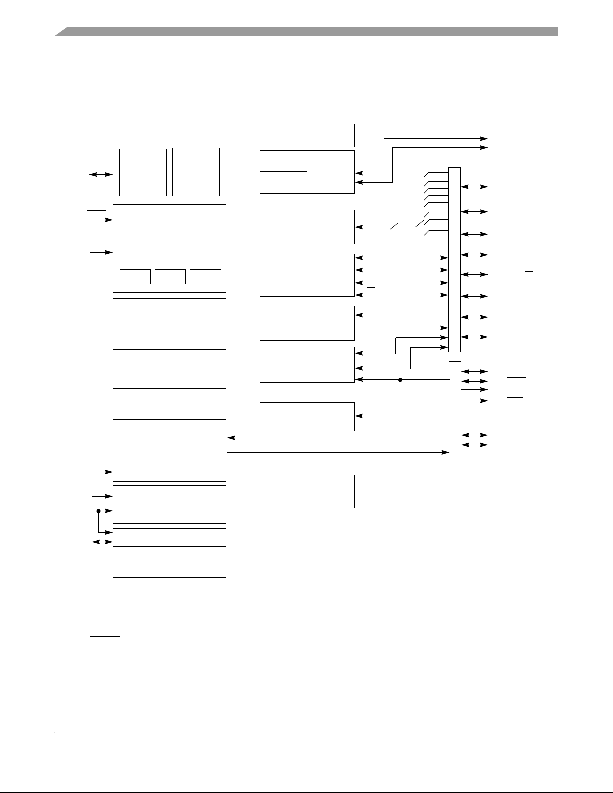
1.2 MCU Block Diagram
The block diagram in Figure 1-1 shows the structure of the MC9S08JS16 series MCU.
Figure 1-1. MC9S08JS16 Series Block Diagram
18 Freescale Semiconductor
MC9S08JS16 MCU Series Reference Manual, Rev. 4
Page 19

Chapter 1 Device Overview
TPM
BDC
CPU
RAM FLASH
2
MCG
MCGOUT
÷2
BUSCLK
MCGLCLK
MCGERCLK
COP
1
The fixed frequency clock (FFCLK) is internally synchronized to the bus clock and must not exceed one half of the
bus clock frequency.
2
Flash and EEPROM have frequency requirements for program and erase operation. See MC9S08JS16 Series
Data Sheet for details.
XOSC
EXTAL XTAL
FFCLK
1
MCGFFCLK
RTC
1 kHz
LPO
TCLK
MCGIRCLK
÷2
USB
USB RAM
SCI
ROM
MTIM
SPI
CRC
Table 1-2 lists the functional versions of the on-chip modules.
Table 1-2. Versions of On-Chip Modules
Module Version
Central Processing Unit (CPU) 2
Keyboard Interrupt (KBI) 2
Multi-Purpose Clock Generator (MCG) 1
Real-Time Counter (RTC) 1
Serial Communications Interface (SCI) 4
Serial Peripheral Interface (SPI16) 1
Modulo Timer (MTIM) 1
Timer Pulse-Width Modulator (TPM) 3
Universal Serial Bus (USB) 1
Cyclic Redundancy Check Generator (CRC) 2
Debug Module (DBG) 2
1.3 System Clock Distribution
TCLK — External input clock source for TPM and MTIM and is referenced as TPMCLK in Chapter 14,
“Timer/Pulse-Width Modulator (S08TPMV3).”
Figure 1-2. System Clock Distribution Diagram
The MCG supplies the following clock sources:
Freescale Semiconductor 19
MC9S08JS16 MCU Series Reference Manual, Rev. 4
Page 20

Chapter 1 Device Overview
• MCGOUT — This clock source is used as the CPU, USB RAM and USB module clock, and is
divided by two to generate the peripheral bus clock (BUSCLK). Control bits in the MCG control
registers determine which of the three clock sources is connected:
— Internal reference clock
— External reference clock
— Frequency-locked loop (FLL) or phase-locked loop (PLL) output
See Chapter 9, “Multi-Purpose Clock Generator (S08MCGV1),” for details on configuring the
MCGOUT clock.
• MCGLCLK — This clock source is derived from the digitally controlled oscillator (DCO) of the
MCG. Development tools can select this internal self-clocked source to speed up BDC
communications in systems where the bus clock is slow.
• MCGIRCLK — This is the internal reference clock and can be selected as the real-time counter
(RTC) clock source. Chapter 9, “Multi-Purpose Clock Generator (S08MCGV1),” explains the
MCGIRCLK in more detail. See Chapter 11, “Real-Time Counter (S08RTCV1),” for more
information regarding the use of MCGIRCLK.
• MCGERCLK — This is the external reference clock and can be selected as the clock source of
RTC module. Section 9.4.6, “External Reference Clock,” explains the MCGERCLK in more
detail. See Chapter 11, “Real-Time Counter (S08RTCV1),” for more information regarding the use
of MCGERCLK with this module.
• MCGFFCLK — This clock source is divided by two to generate FFCLK after being synchronized
to the BUSCLK. It can be selected as clock source for the TPM or MTIM modules. The frequency
of the MCGFFCLK is determined by the settings of the MCG. See Section 9.4.7, “Fixed Frequency
Clock,” for details.
• LPO clock — This clock is generated from an internal low power oscillator that is completely
independent of the MCG module. The LPO clock can be selected as the clock source to the RTC
or COP modules. See Chapter 11, “Real-Time Counter (S08RTCV1),” and Section 5.4, “Computer
Operating Properly (COP) Watchdog,” for details on using the LPO clock with these modules.
• TCLK — TCLK is the optional external clock source for the TPM or MTIM modules. The TCLK
must be limited to 1/4th the frequency of the BUSCLK for synchronization. See Chapter 14,
“Timer/Pulse-Width Modulator (S08TPMV3),” for more details.
MC9S08JS16 MCU Series Reference Manual, Rev. 4
20 Freescale Semiconductor
Page 21

Chapter 2
USBDN
PTB3/BLMS
1
2
3
4
5
PTA0/KBIP0/TPMCH0
81011
7
17
23
PTB2/BKGD/MS
13
14
15
16
22 21 20 19
PTB5/EXTAL
V
SSOSC
PTA5/KBIP5/TPMCH1
V
USB33
V
DD
PTA4/KBIP4/SS
PTA2/KBIP2/MOSI
PTA1/KBIP1/MISO
PTA7/KBIP7/TxD
PTB4/XTAL
PTA3/KBIP3/SPSCK
PTB1/RESET
PTB0/IRQ/TCLK
USBDP
V
SS
PTA6/KBIP6/RxD
24-Pin QFN
12
NC
6
NC
V
SS
NC
18
24
NC
9
Pins and Connections
2.1 Introduction
This chapter describes signals that connect to package pins. It includes a pinout diagram, a table of signal
properties, and detailed discussion of signals.
2.2 Device Pin Assignment
Freescale Semiconductor 21
Figure 2-1. MC9S08JS16 Series in 24-pin QFN Package
MC9S08JS16 MCU Series Reference Manual, Rev. 4
Page 22

Chapter 2 Pins and Connections
1
2
3
4
5
6
7
8
9
10
20
19
18
17
16
15
14
13
12
11
PTA3/KBIP3/SPSCK
PTA4/KBIP4/SS
USBDP
USBDN
V
USB33
PTA5/KBIP5/TPMCH1
V
DD
V
SS
V
SSOSC
PTB0/IRQ/TCLK
PTB1/RESET
PTA0/KBIP0/TPMCH0
PTA1/KBIP1/MISO
PTA2/KBIP2/MOSI
PTA7/KBIP7/TxD
PTA6/KBIP6/RxD
PTB5/EXTAL
PTB4/XTAL
PTB2/BKGD/MS
PTB3/BLMS
Figure 2-2. MC9S08JS16 Series in 20-Pin SOIC Package
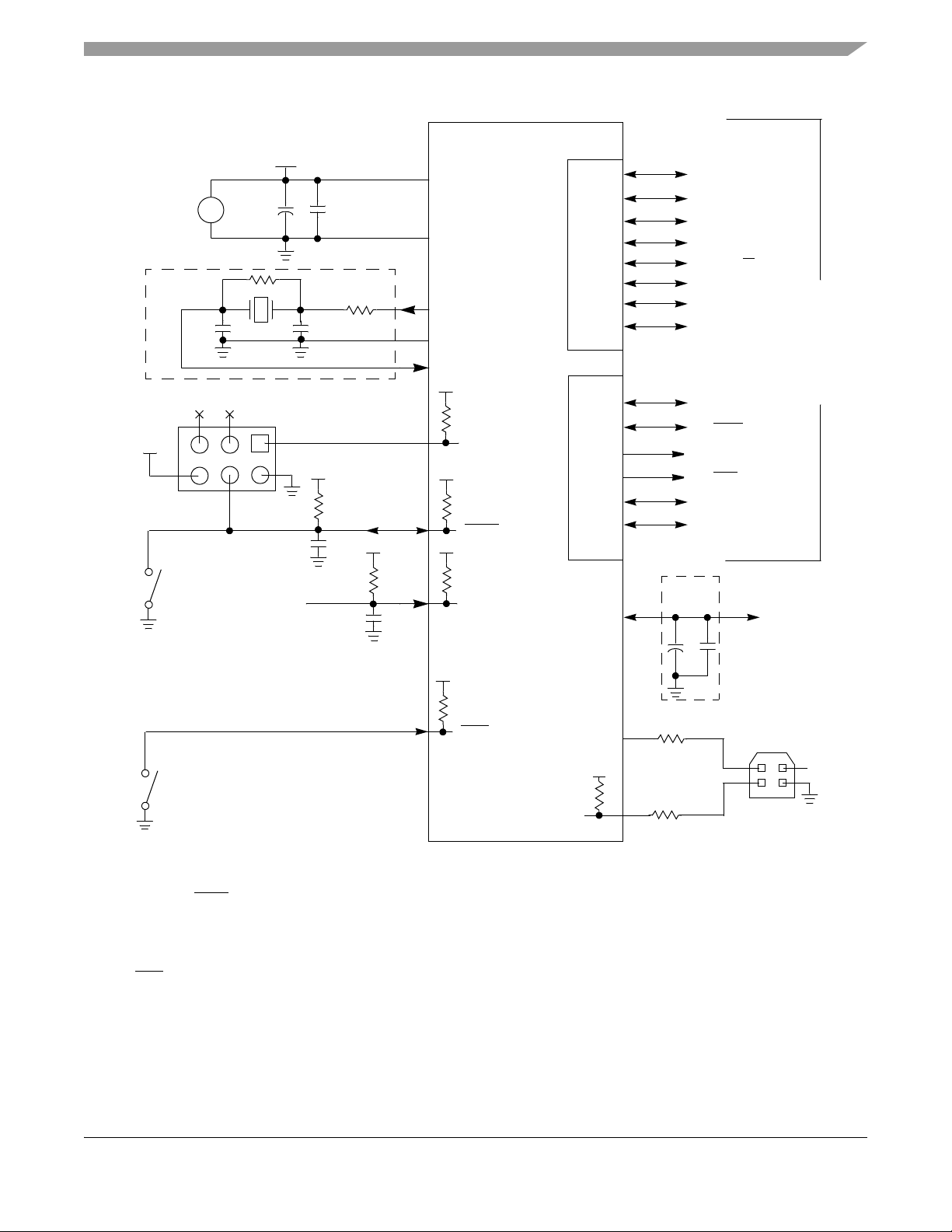
2.3 Recommended System Connections
Figure 2-3 shows pin connections that are common to almost all MC9S08JS16 series application systems.
22 Freescale Semiconductor
MC9S08JS16 MCU Series Reference Manual, Rev. 4
Page 23
V
DD
V
SS
RESET
OPTIONAL
MANUAL
RESET
V
DD
1
BACKGROUND HEADER
C
BY
0.1 μF
C
BLK
10 μF
+
5 V
+
SYSTEM
POWER
I/O AND
PERIPHERAL
INTERFACE TO
SYSTEM
APPLICATION
V
DD
PORT
A
PORT
B
IRQ
ASYNCHRONOUS
INTERRUPT
INPUT
NOTES:
1. External crystal circuity is not required if using the MCG internal clock. For USB operation, an external crystal is required.
2. XTAL and EXTAL use the same pins as PTB4 and PTB5, respectively.
3. RC filters on RESET
and IRQ are recommended for EMC-sensitive applications.
4. R
PUDP
is shown for full-speed USB only. The diagram shows a configuration where the on-chip regulator and R
PUDP
are enabled. The voltage regulator output is
used for R
PUDP. RPUDP
can optionally be disabled if using an external pullup resistor on USBDP.
5. V
BUS
is a 5.0 V supply from upstream port that can be used for USB operation.
6. USBDP and USBDN are powered by the 3.3 V regulator.
7. For USB operation, an external crystal with a value of 2 MHz or 4 MHz is recommended.
8. BLMS
pin has loading limitation, do not connect any cap with this pin.
9. If there is an external pullup resistor on PTB2/PTB3, PTB2/PTB3 must be configured as anoutput pin. Otherwise there will be current consumption on the pin (about
0.5 mA for a 10 kΩ resistor). The load on PTB2/PTB3 must be smaller than 50 pF.
10. When using internal V
USB33
as supply, there needs to be an external cap.
MC9S08JS16
V
DD
4.7 kΩ
–
0
.1 μF
V
DD
4.7 kΩ–10 kΩ
0.1 μF
1
0 kΩ
2
43
USBDN
V
USB33
USBDP
V
Bus
USB SERIES-B CONNECTOR
V
USB33
3.3 V Reference
R
PUDP
BKGD/MS
XTAL
EXTAL
C2
C1
X1
R
F
R
S
NOTE 1
V
SSOSC
PTB3/BLMS
PTB2/BKGD/MS
PTB0/IRQ/TCLK
PTB1/RESET
PTB5/EXTAL
PTB4/XTAL
PTA2/KBIP2/MOSI
PTA3/KBIP3/SPSCK
PTA6/KBIP6/RxD
PTA7/KBIP7/TxD
PTA4/KBIP4/SS
PTA5/KBIP5/TPMCH1
PTA0/KBIP0/TPMCH0
PTA1/KBIP1/MISO
BLMS
OPTIONAL
MANUAL
BLMS
NOTE 8, 9
C
4
0.47 μF
C
3
4.7 μF
+
NOTE 10
33 Ω ± 1%
33 Ω ± 1%
Chapter 2 Pins and Connections
Freescale Semiconductor 23
Figure 2-3. Basic System Connections
MC9S08JS16 MCU Series Reference Manual, Rev. 4
Page 24

Chapter 2 Pins and Connections
2.3.1 Power (VDD, VSS, V
SSOSC
, V
USB33
)
VDD and VSS are the primary power supply pins for the MCU. This voltage source supplies power to all
I/O buffer circuitry and to an internal voltage regulator. The internal voltage regulator provides regulated
lower-voltage source to the CPU and other internal circuitry of the MCU.
Typically, application systems have two separate capacitors across the power pins. In this case, there must
be a bulk electrolytic capacitor, such as a 10 μF tantalum capacitor, to provide bulk charge storage for the
overall system and a 0.1 μF ceramic bypass capacitor located as near to the paired VDD and V
pins as practical to suppress high-frequency noise. The MC9S08JS16 has a V
pin. This pin must be
SSOSC
SS
power
connected to the system ground plane or to the primary VSS pin through a low-impedance connection.
V
Controller (S08USBV1),” for a complete description of the V
is connected to the internal USB 3.3 V regulator. See Chapter 15, “Universal Serial Bus Device
USB33
power pin.
USB33
2.3.2 Oscillator (XTAL, EXTAL)
Immediately after reset, the MCU uses an internally generated clock provided by the multi-purpose clock
generator (MCG) module. For more information on the MCG, see Chapter 9, “Multi-Purpose Clock
Generator (S08MCGV1).”
The oscillator (XOSC) in this MCU is a Pierce oscillator that can accommodate a crystal or ceramic
resonator. Rather than a crystal or ceramic resonator, an external oscillator can be connected to the EXTAL
input pin.
RS (when used) and RF must be low-inductance resistors such as carbon composition resistors.
Wire-wound resistors, and some metal film resistors, have too much inductance. C1 and C2 normally are
high-quality ceramic capacitors that are specifically designed for high-frequency applications.
RF is used to provide a bias path to keep the EXTAL input in its linear range during crystal startup; its value
is not generally critical. Typical systems use 1 MΩ to 10 MΩ. Higher values are sensitive to humidity and
lower values reduce gain and (in extreme cases) could prevent startup.
C1 and C2 are typically in the 5 pF to 25 pF range and are chosen to match the requirements of a specific
crystal or resonator. Be sure to take into account printed circuit board (PCB) capacitance and MCU pin
capacitance when selecting C1 and C2. The crystal manufacturer typically specifies a load capacitance that
is the series combination of C1 and C2 (which are usually the same size). As a first-order approximation,
use 10 pF as an estimate of combined pin and PCB capacitance for each oscillator pin (EXTAL and
XTAL).
2.3.3 RESET Pin
After a power-on reset (POR), the PTB1/RESET pin defaults to a general-purpose input port pin, PTB1.
Setting RSTPE in SOPT1 configures the pin to be the RESET pin containing an internal pullup device.
After configured as RESET
enabled can be used to reset the MCU from an external source when the pin is driven low.
, the pin remains RESET until the next LVD or POR. The RESET pin when
MC9S08JS16 MCU Series Reference Manual, Rev. 4
24 Freescale Semiconductor
Page 25

Chapter 2 Pins and Connections
Internal power-on reset and low-voltage reset circuitry typically make external reset circuitry unnecessary.
This pin is normally connected to the standard 6-pin background debug connector so a development
system can directly reset the MCU system. If desired, a manual external reset can be added by supplying
a simple switch to ground (pull reset pin low to force a reset).
When any non-POR reset is initiated (whether from an external source or from an internal source), the
RESET pin is driven low for approximately 66 bus cycles and released. The reset circuity decodes the
cause of reset and records it by setting a corresponding bit in the system control reset status register (SRS).
NOTE
The voltage on the internally pulled up RESET pin when measured is below
VDD. The internal gates connected to this pin are pulled to VDD. If the
RESET pin is required to drive to a V
level, an external pullup must be
DD
used.
NOTE
In EMC-sensitive applications, an external RC filter is recommended on the
RESET pin, if enabled (Figure 2-3).
2.3.4 Background/Mode Select (BKGD/MS)
During a power-on-reset (POR) or background debug force reset (see Section 5.7.3, “System Background
Debug Force Reset Register (SBDFR),” for details), the PTB2/BKGD/MS pin functions as a mode select
pin. Immediately after reset rises the pin functions as the background pin and can be used for background
debug communication. When enabled as the BKGD/MS pin (BKGDPE = 1), an internal pullup device is
automatically enabled.
The background debug communication function is enabled when BKGDPE in SOPT1 is set. BKGDPE is
set following any reset of the MCU and must be cleared to use the PTB2/BKGD/MS pin’s alternative pin
functions.
If nothing is connected to this pin, the MCU will enter normal operating mode at the rising edge of reset.
If a debug system is connected to the 6-pin standard background debug header, it can hold BKGD/MS low
during the rising edge of reset which forces the MCU to active background mode.
The BKGD pin is used primarily for background debug controller (BDC) communications using a custom
protocol that uses 16 clock cycles of the target MCU’s BDC clock per bit time. The target MCU’s BDC
clock could be as fast as the bus clock rate, so there must never be any significant capacitance connected
to the BKGD/MS pin that could interfere with background serial communications.
Although the BKGD pin is a pseudo open-drain pin, the background debug communication protocol
provides brief, actively driven, high speedup pulses to ensure fast rise times. Small capacitances from
cables and the absolute value of the internal pullup device play almost no role in determining rise and fall
times on the BKGD pin.
MC9S08JS16 MCU Series Reference Manual, Rev. 4
Freescale Semiconductor 25
Page 26

Chapter 2 Pins and Connections
NOTE
Before the IRQ or RESET function is enabled, be sure to enable the GPIO
pullup in that function’s pin and wait about 2 μs. Otherwise the IRQ or
RESET configuration may fail.
2.3.5 Bootloader Mode Select (BLMS)
During a power-on-reset (POR), the CPU detects the state of the PTB3/BLMS pin that functions as a mode
select pin. When the logic is low and BKGD/MS is not pulled low, the CPU enters the bootloader mode.
During a power-on-reset (POR), an internal pullup device is automatically enabled in PTB3/BLMS pin.
Immediately after reset rises the pin functions as a general-purpose output only pin and an internal pullup
device is automatically disabled.
2.3.6 USB Data Pins (USBDP, USBDN)
The USBDP (D+) and USBDN (D–) pins are the analog input/output lines for full-speed data
communication in the USB physical layer (PHY) module. An optional internal pullup resistor for the
USBDP pin, R
, is available.
PUDP
2.3.7 General-Purpose I/O and Peripheral Ports
The MC9S08JS16 series of MCUs supports up to 14 general-purpose I/O pins, including two output-only
pins, which are shared with on-chip peripheral functions (timers, serial I/O, keyboard interrupts, etc.).
When a port pin is configured as a general-purpose output or a peripheral uses the port pin as an output,
software can select one of two drive strengths and enable or disable slew rate control. When a port pin is
configured as a general-purpose input or a peripheral uses the port pin as an input, software can enable a
pullup device.
For information about controlling these pins as general-purpose I/O pins, see Chapter 6, “Parallel
Input/Output.” For information about how and when on-chip peripheral systems use these pins, see the
appropriate module chapter.
Immediately after reset, all pins except the output-only pin (PTB2/BKGD/MS, PTB3/BLMS) are
configured as high-impedance general-purpose inputs with internal pullup devices disabled.
Table 2-1. Pin Availability by Package Pin-Count
Pin Number
(Package)
24 (QFN) 20 (SOIC) Port Pin Alt 1 Alt 2
1 4 PTB0 IRQ TCLK
<-- Lowest Priority --> Highest
2 5 PTB1 RESET
3 6 PTB2 BKGD MS
4 7 PTB3 BLMS
MC9S08JS16 MCU Series Reference Manual, Rev. 4
26 Freescale Semiconductor
Page 27

Chapter 2 Pins and Connections
Table 2-1. Pin Availability by Package Pin-Count (continued)
Pin Number
(Package)
24 (QFN) 20 (SOIC) Port Pin Alt 1 Alt 2
5 8 PTA0 KBIP0 TPMCH0
6—NC
7 9 PTA1 KBIP1 MISO
8 10 PTA2 KBIP2 MOSI
9 11 PTA3 KBIP3 SPSCK
10 12 PTA4 KBIP4 SS
11 13 V
12 — NC
13 14 V
14 15 USBDN
15 16 USBDP
16 17 V
17 18 PTA5 KBIP5 TPMCH1
18 — NC
<-- Lowest Priority --> Highest
DD
SS
USB33
19 19 PTA6 KBIP6 RxD
20 20 PTA7 KBIP7 TxD
21 1 PTB4 XTAL
22 2 PTB5 EXTAL
23 3 V
24 — NC
SSOSC
NOTE
When an alternative function is first enabled, it is possible to get a spurious
edge to the module. User software must clear any associated flags before
interrupts are enabled. Table 2-1 illustrates the priority if multiple modules
are enabled. The highest priority module will have control over the pin.
Selecting a higher priority pin function with a lower priority function
already enabled can cause spurious edges to the lower priority module. All
modules that share a pin must be disabled before another module is enabled.
MC9S08JS16 MCU Series Reference Manual, Rev. 4
Freescale Semiconductor 27
Page 28

Chapter 2 Pins and Connections
MC9S08JS16 MCU Series Reference Manual, Rev. 4
28 Freescale Semiconductor
Page 29

Chapter 3 Modes of Operation
3.1 Introduction
The operating modes of the MC9S08JS16 series are described in this section. Entry into each mode, exit
from each mode, and functionality while in each mode are described.
3.2 Features
• Active background mode for code development
• Wait mode:
— CPU halts operation to conserve power
— System clocks keep running
— Full voltage regulation is maintained
• Stop modes: CPU and bus clocks stopped
— Stop2: Partial power down of internal circuits; RAM and USB RAM contents retained
— Stop3: All internal circuits powered for fast recovery; RAM, USB RAM, and register contents
are retained
3.3 Run Mode
Run is the normal operating mode for the MC9S08JS16 series. This mode is selected upon the MCU
exiting reset if the BKGD/MS pin is high. In this mode, the CPU executes code from internal memory with
execution beginning at the address fetched from memory at 0xFFFE:0xFFFF after reset.
3.4 Active Background Mode
The active background mode functions are managed through the background debug controller (BDC) in
the HCS08 core. The BDC, together with the on-chip in-circuit emulator (ICE) debug module (DBG),
provides the means for analyzing MCU operation during software development.
Active background mode is entered in any of the following ways:
• When the BKGD/MS pin is low during POR or immediately after issuing a background debug
force reset (see Section 5.7.3, “System Background Debug Force Reset Register (SBDFR)”)
• When a BACKGROUND command is received through the BKGD pin
• When a BGND instruction is executed
• When encountering a BDC breakpoint
• When encountering a DBG breakpoint
MC9S08JS16 MCU Series Reference Manual, Rev. 4
Freescale Semiconductor 29
Page 30

Chapter 3 Modes of Operation
After entering active background mode, the CPU is held in a suspended state waiting for serial background
commands rather than executing instructions from the user application program.
Background commands are of two types:
• Non-intrusive commands, defined as commands that can be issued while the user program is
running. Non-intrusive commands can be issued through the BKGD pin while the MCU is in run
mode; non-intrusive commands can also be executed when the MCU is in the active background
mode. Non-intrusive commands include:
— Memory access commands
— Memory-access-with-status commands
— BDC register access commands
— The BACKGROUND command
• Active background commands, which can only be executed while the MCU is in active background
mode. Active background commands include commands to:
— Read or write CPU registers
— Trace one user program instruction at a time
— Leave active background mode to return to the user application program (GO)
The active background mode is used to program a bootloader or user application program into the flash
program memory before the MCU is operated in run mode for the first time. When the MC9S08JS16 series
devices are shipped from the Freescale factory, the flash program memory is erased by default unless
specifically noted, so there is no program that could be executed in run mode until the flash memory is
initially programmed. The active background mode can also be used to erase and reprogram the flash
memory after it has been previously programmed.
For additional information about the active background mode, refer to Chapter 17, “Development
Support.”
3.5 Wait Mode
Wait mode is entered by executing a WAIT instruction. Upon execution of the WAIT instruction, the CPU
enters a low-power state in which it is not clocked. The I bit in the condition code register (CCR) is cleared
when the CPU enters wait mode, enabling interrupts. When an interrupt request occurs, the CPU exits wait
mode and resumes processing, beginning with the stacking operations leading to the interrupt service
routine.
While the MCU is in wait mode, there are some restrictions on which background debug commands can
be used. Only the BACKGROUND command and memory-access-with-status commands are available
while the MCU is in wait mode. The memory-access-with-status commands do not allow memory access,
but they report an error indicating that the MCU is in stop or wait mode. The BACKGROUND command
can be used to wake the MCU from wait mode and enter active background mode.
MC9S08JS16 MCU Series Reference Manual, Rev. 4
30 Freescale Semiconductor
Page 31

Chapter 3 Modes of Operation
3.6 Stop Modes
One of two stop modes is entered upon execution of a STOP instruction when STOPE in SOPT1 is set. In
any stop mode, the bus and CPU clocks are halted. The MCG module can be configured to leave the
reference clocks running. See Chapter 9, “Multi-Purpose Clock Generator (S08MCGV1),” for more
information.
Some HCS08 devices that are designed for low-voltage operation (1.8 to 3.6 V) also include stop1 mode.
The MC9S08JS16 series of MCUs do not include stop1 mode.
Table 3-1 shows all of the control bits that affect stop mode selection and the mode selected under various
conditions. The selected mode is entered following the execution of a STOP instruction.
Table 3-1. Stop Mode Selection
STOPE ENBDM
0 x x x Stop modes disabled; illegal opcode reset if STOP
1 1 x x Stop3 with BDM enabled
1 0 Both bits must be 1 x Stop3 with voltage regulator active
1 0 Either bit a 0 0 Stop3
1 0 Either bit a 0 1 Stop2
1
ENBDM is located in the BDCSCR which is only accessible through BDC commands, see Section 14.4.1.1,
“BDC Status and Control Register (BDCSCR).”
2
When in stop3 mode with BDM enabled, The S
enabled.
1
LVD E LVD S E PP D C St o p M o de
instruction executed
will be near R
IDD
levels because internal clocks are
IDD
2
3.6.1 Stop3 Mode
Stop3 mode is entered by executing a STOP instruction under the conditions shown in Tabl e 3- 1. The
states of all of the internal registers and logic, RAM contents, and I/O pin states are maintained.
Stop3 can be exited by asserting RESET, or by an interrupt from one of the following sources: the real-time
clock (RTC) interrupt, the USB resume interrupt, LVD, IRQ, KBI, or the SCI.
If stop3 is exited by the RESET pin, then the MCU is reset and operation will resume after taking the reset
vector. Exit by one of the internal interrupt sources results in the MCU taking the appropriate interrupt
vector.
3.6.1.1 LVD Enabled in Stop Mode
The LVD system is capable of generating an interrupt or a reset when the supply voltage drops below the
LVD voltage. If the LVD is enabled in stop (LVDE and LVDSE bits in SPMSC1 both set) at the time the
CPU executes a STOP instruction, then the voltage regulator remains active during stop mode. If the user
attempts to enter stop2 with the LVD enabled for stop, the MCU will enter stop3 instead.
MC9S08JS16 MCU Series Reference Manual, Rev. 4
Freescale Semiconductor 31
Page 32

Chapter 3 Modes of Operation
For the XOSC to operate with an external reference when RANGE in MCGC2 is set, the LVD must be left
enabled when entering stop3.
NOTE
To get low USB suspend current, before entering USB suspend mode, we
must set ERCLKEN and EREFSTEN in MCGC2, but leave LVD disabled
in stop3.
3.6.1.2 Active BDM Enabled in Stop Mode
Entry into the active background mode from run mode is enabled if ENBDM in BDCSCR is set. This
register is described in Chapter 17, “Development Support.” If ENBDM is set when the CPU executes a
STOP instruction, the system clocks to the background debug logic remain active when the MCU enters
stop mode. Because of this, background debug communication remains possible. In addition, the voltage
regulator does not enter its low-power standby state but maintains full internal regulation. If the user
attempts to enter stop2 with ENBDM set, the MCU will enter stop3 instead.
Most background commands are not available in stop mode. The memory-access-with-status commands
do not allow memory access, but they report an error indicating that the MCU is in stop or wait mode. The
BACKGROUND command can be used to wake the MCU from stop and enter active background mode
if the ENBDM bit is set. After entering background debug mode, all background commands are available.
3.6.2 Stop2 Mode
Stop2 mode is entered by executing a STOP instruction under the conditions as shown in Table 3- 1. Most
of the internal circuitry of the MCU is powered off in stop2, with the exception of the RAM. Upon entering
stop2, all I/O pin control signals are latched so that the pins retain their states during stop2.
Exit from stop2 is performed by asserting either wakeup pin: RESET or IRQ. When an application utilizes
the stop2 state, RESET or IRQ pin must be pre-configured as an input prior to entering stop2. There is a
direct analog connection from RESET or IRQ pad to the power management controller wakeup pin — if
configured as a GPIO output, it could prevent operation of stop2.
In addition, the RTC interrupt can wake the MCU from stop2, if enabled.
Upon wakeup from stop2 mode, the MCU starts up as from a power-on reset (POR):
• All module control and status registers are reset
• The LVD reset function is enabled and the MCU remains in the reset state if V
trip point (low trip point selected due to POR)
• The CPU takes the reset vector
In addition to the above, upon waking from stop2, the PPDF bit in SPMSC2 is set. This flag is used to
direct user code to go to a stop2 recovery routine. PPDF remains set and the I/O pin states remain latched
until a 1 is written to PPDACK in SPMSC2.
is below the LVD
DD
To maintain I/O states for pins that are configured as general-purpose I/O before entering stop2, the user
must restore the contents of the I/O port registers, which have been saved in RAM, to the port registers
MC9S08JS16 MCU Series Reference Manual, Rev. 4
32 Freescale Semiconductor
Page 33

Chapter 3 Modes of Operation
before writing to the PPDACK bit. If the port registers are not restored from RAM before writing to
PPDACK, then the pins will switch to their reset states when PPDACK is written.
For pins that are configured as peripheral I/O, the user must reconfigure the peripheral module that
interfaces to the pin before writing to the PPDACK bit. If the peripheral module is not enabled before
writing to PPDACK, the pins will be controlled by their associated port control registers when the I/O
latches are opened.
3.6.3 On-Chip Peripheral Modules in Stop Modes
When the MCU enters any stop mode, system clocks to the internal peripheral modules are stopped. Even
in the exception case (ENBDM = 1), where clocks to the background debug logic continue to operate,
clocks to the peripheral systems are halted to reduce power consumption. Refer to Section 3.6.2, “Stop2
Mode,” and Section 3.6.1, “Stop3 Mode,” for specific information on system behavior in stop modes.
Table 3-2. Stop Mode Behavior
Mode
Peripheral
CPU Off Standby
RAM Standby Standby
Flash Off Standby
Parallel Port Registers Off Standby
MCG Off Optionally On
RTC Optionally on
SCI Off Standby
SPI Off Standby
MTIM Off Standby
TPM Off Standby
System Voltage Regulator Off Standby
XOSC Off Optionally On
I/O Pins States Held States Held
USB (SIE and PHY) Off Optionally On
USB 3.3 V Regulator Off Standby
USB RAM Standby Standby
CRC Off Standby
1
IREFSTEN set in MCGC1, else in standby.
2
RTCPS[3:0] in RTCSC does not equal 0 before entering stop, else off.
3
EREFSTEN set in MCGC2, else in standby. For high frequency range (RANGE in
MCGC2 set), the LVD must also be enabled in stop3.
4
USBEN in CTL is set and USBPHYEN in USBCTL0 is set, else off.
Stop2 Stop3
2
Optionally on
1
2
3
4
MC9S08JS16 MCU Series Reference Manual, Rev. 4
Freescale Semiconductor 33
Page 34

Chapter 3 Modes of Operation
MC9S08JS16 MCU Series Reference Manual, Rev. 4
34 Freescale Semiconductor
Page 35

Chapter 4 Memory
4.1 MC9S08JS16 Series Memory Map
Figure 4-1 shows the memory map for the MC9S08JS16 series. On-chip memory in the MC9S08JS16
series of MCUs consists of RAM, flash program memory for nonvolatile data storage, plus I/O and
control/status registers. The registers are divided into three groups:
• Direct-page registers (0x0000 through 0x007F)
• High-page registers (0x1800 through 0x185F)
• Nonvolatile registers (0xFFB0 through 0xFFBF)
MC9S08JS16 MCU Series Reference Manual, Rev. 4
Freescale Semiconductor 35
Page 36

Chapter 4 Memory
DIRECT-PAGE REGISTERS
RAM
HIGH-PAGE REGISTERS
512 BYTES
0x0000
0x007F
0x0080
0x027F
0x1800
0x17FF
0x185F
0xFFFF
0x0280
MC9S08JS16
MC9S08JS16L
FLASH
16,384 BYTES
0x1860
UNIMPLEMENTED
0xC000
0xBFFF
UNIMPLEMENTED
USB Buffer RAM
0x195F
0x1960
(256 BYTES)
0x3160
0x315F
Bootloader ROM
(4096 BYTES)
0x2160
0x215F
UNIMPLEMENTED
(2048 BYTES)
MC9S08JS8
MC9S08JS8L
FLASH
8,192 BYTES
0xE000
RESERVED
8,192 BYTES
0xDFFF
DIRECT-PAGE REGISTERS
RAM
HIGH-PAGE REGISTERS
512 BYTES
0x0000
0x007F
0x0080
0x027F
0x1800
0x17FF
0x185F
0xFFFF
0x0280
0x1860
UNIMPLEMENTED
0xC000
0xBFFF
UNIMPLEMENTED
USB Buffer RAM
0x195F
0x1960
(256 BYTES)
0x3160
0x315F
Bootloader ROM
(4096 BYTES)
0x2160
0x215F
UNIMPLEMENTED
(2048 BYTES)
4.1.1 Reset and Interrupt Vector Assignments
Table 4-1 shows address assignments for reset and interrupt vectors. The vector names shown in this table
are the labels used in the Freescale-provided equate file for the MC9S08JS16 series. For more details about
resets, interrupts, interrupt priority, and local interrupt mask controls, refer to Chapter 5, “Resets,
Interrupts, and System Configuration.”
Figure 4-1. MC9S08JS16 Series Memory Map
36 Freescale Semiconductor
MC9S08JS16 MCU Series Reference Manual, Rev. 4
Page 37

Table 4-1. Reset and Interrupt Vectors
Chapter 4 Memory
Address
(High/Low)
0xFFC0:0xFFC1
to
0xFFC2:FFC3
0xFFC4:FFC5 RTC Vrtc
0xFFC6:FFC7 Unused vector space —
0xFFC8:FFC9 Unused vector space —
0xFFCA:FFCB MTIM Vmtim
0xFFCC:FFCD KBI Vkeyboard
0xFFCE:FFCF
to
0xFFD2:FFD3
0xFFD4:FFD5 SCI Transmit Vscitx
0xFFD6:FFD7 SCI Receive Vscirx
0xFFD8:FFD9 SCI Error Vscierr
0xFFDA:FFDB
to
0xFFE6:FFE7
Vector Vector Name
Unused vector space
Unused vector space —
Reserved —
1
—
0xFFE8:FFE9 TPM Overflow Vtpmovf
0xFFEA:FFEB TPM Channel 1 Vtpmch1
0xFFEC:FFED TPM Channel 0 Vtpmch0
0xFFEE:FFEF Unused vector space —
0xFFF0:FFF1 USB Status Vusb
0xFFF2:FFF3 Unused vector space —
0xFFF4:FFF5 SPI Vspi
0xFFF6:FFF7 MCG Loss of Lock Vlol
0xFFF8:FFF9 Low Voltage Detect Vlvd
0xFFFA:FFFB IRQ Virq
0xFFFC:FFFD SWI Vswi
0xFFFE:FFFF Reset Vreset
1
Unused vector space is available for use as general flash memory. However, other
devices in the S08 family of MCUs may use these locations as interrupt vectors.
Therefore, care must be taken when using these locations if the code will be
ported to other MCUs.
4.2 Register Addresses and Bit Assignments
The registers in the MC9S08JS16 series are divided into these three groups:
MC9S08JS16 MCU Series Reference Manual, Rev. 4
Freescale Semiconductor 37
Page 38

Chapter 4 Memory
• Direct-page registers are located in the first 128 locations in the memory map, so they are
accessible with efficient direct addressing mode instructions.
• High-page registers are used much less often, so they are located above 0x1800 in the memory
map. This leaves more room in the direct-page for more frequently used registers and variables.
• The nonvolatile register area consists of a block of 16 locations in flash memory at
0xFFB0–0xFFBF.
Nonvolatile register locations include:
— Three values that are loaded into working registers at reset
— An 8-byte backdoor comparison key that optionally allows a user to gain controlled access to
secure memory
Because the nonvolatile register locations are flash memory, they must be erased and programmed
like other flash memory locations.
Direct-page registers can be accessed with efficient direct addressing mode instructions. Bit manipulation
instructions can be used to access any bit in any direct-page register. Tab le 4-2 is a summary of all
user-accessible direct-page registers and control bits.
The direct-page registers in Table 4-2 can use the more efficient direct addressing mode that requires only
the lower byte of the address. Because of this, the lower byte of the address in column one is shown in bold
text. In Table 4-3 and Ta ble 4-4 the whole address in column one is shown in bold. In Tab l e 4- 2, Table 4-3,
and Tabl e 4-4, the register names in column two are shown in bold to set them apart from the bit names to
the right. Cells that are not associated with named bits are shaded. A shaded cell with a 0 indicates this
unused bit always reads as a 0. Shaded cells with dashes indicate unused or reserved bit locations that could
read as 1s or 0s.
MC9S08JS16 MCU Series Reference Manual, Rev. 4
38 Freescale Semiconductor
Page 39

Table 4-2. Direct-Page Register Summary (Sheet 1 of 3)
Chapter 4 Memory
Address
Register
Name
Bit 7 6 5 4 3 2 1 Bit 0
0x0000 PTAD PTAD7 PTAD6 PTAD5 PTAD4 PTAD3 PTAD2 PTAD1 PTAD0
0x0001 PTADD PTADD7 PTADD6 PTADD5 PTADD4 PTADD3 PTADD2 PTADD1 PTADD0
0x0002 PTBD
0x0003 PTBDD
0x0004–
Reserved
0x0007
0 0 PTBD5 PTBD4 PTBD3 PTBD2 PTBD1 PTBD0
0 0 PTBDD5 PTBDD4 R R PTBDD1 PTBDD0
—
—
—
—
—
—
—
—
—
—
—
—
—
—
—
—
0x0008 MTIMSC TOF TOIE TRST TSTP 0 0 0 0
0x0009 MTIMCLK
0 0CLKS PS
0x000A MTIMCNT COUNT
0x000B MTIMMOD MOD
0x000C CRCH Bit 15 14 13 12 11 10 9 Bit 8
0x000D CRCL Bit 7 6 5 4 3 2 1 Bit 0
0x000E Reserved
0x000F Reserved
— — — — — — — —
— — — — — — — —
0x0010 TPMSC TOF TOIE CPWMS CLKSB CLKSA PS2 PS1 PS0
0x0011 TPMCNTH Bit 15 14 13 12 11 10 9 Bit 8
0x0012 TPMCNTL Bit 7 6 5 4 3 2 1 Bit 0
0x0013 TPMMODH Bit 15 14 13 12 11 10 9 Bit 8
0x0014 TPMMODL Bit 7 6 5 4 3 2 1 Bit 0
0x0015 TPMC0SC CH0F CH0IE MS0B MS0A ELS0B ELS0A
0 0
0x0016 TPMC0VH Bit 15 14 13 12 11 10 9 Bit 8
0x0017 TPMC0VL Bit 7 6 5 4 3 2 1 Bit 0
0x0018 TPMC1SC CH1F CH1IE MS1B MS1A ELS1B ELS1A
0 0
0x0019 TPMC1VH Bit 15 14 13 12 11 10 9 Bit 8
0x001A TPMC1VL Bit 7 6 5 4 3 2 1 Bit 0
0x001B IRQSC
0 IRQPDD IRQEDG IRQPE IRQF IRQACK IRQIE IRQMOD
0x001C KBISC 0 0 0 0 KBF KBACK KBIE KBMOD
0x001D KBIPE KBIPE7 KBIPE6 KBIPE5 KBIPE4 KBIPE3 KBIPE2 KBIPE1 KBIPE0
0x001E KBIES KBEDG7 KBEDG6 KBEDG5 KBEDG4 KBEDG3 KBEDG2 KBEDG1 KBEDG0
0x001F Reserved
0x0020 SCIBDH LBKDIE RXEDGIE
— — — — — — — —
0 SBR12 SBR11 SBR10 SBR9 SBR8
0x0021 SCIBDL SBR7 SBR6 SBR5 SBR4 SBR3 SBR2 SBR1 SBR0
0x0022 SCIC1 LOOPS SCISWAI RSRC M WAKE ILT PE PT
0x0023 SCIC2 TIE TCIE RIE ILIE TE RE RWU SBK
0x0024 SCIS1 TDRE TC RDRF IDLE OR NF FE PF
0x0025 SCIS2 LBKDIF RXEDGIF
0 RXINV RWUID BRK13 LBKDE RAF
0x0026 SCIC3 R8 T8 TXDIR TXINV ORIE NEIE FEIE PEIE
0x0027 SCID Bit 7 6 5 4 3 2 1 Bit 0
0x0028–
0x002F
Reserved
— — — — — — — —
0x0030 SPIC1 SPIE SPE SPTIE MSTR CPOL CPHA SSOE LSBFE
0x0031 SPIC2 SPMIE SPIMODE 0 MODFEN BIDIROE 0 SPISWAI SPC0
MC9S08JS16 MCU Series Reference Manual, Rev. 4
Freescale Semiconductor 39
Page 40

Chapter 4 Memory
Table 4-2. Direct-Page Register Summary (Sheet 2 of 3)
Address
0x0032 SPIBR
0x0033 SPIS SPRF SPMF SPTEF MODF
Register
Name
Bit 7 6 5 4 3 2 1 Bit 0
0 SPPR2 SPPR1 SPPR0 0 SPR2 SPR1 SPR0
0 0 0 0
0x0034 SPIDH Bit 15 14 13 12 11 10 9 Bit 8
0x0035 SPIDL Bit 7 6 5 4 3 2 1 Bit 0
0x0036 SPIMH Bit 15 14 13 12 11 10 9 Bit 8
0x0037 SPIML Bit 7 6 5 4 3 2 1 Bit 0
0x0038–
0x003F
Reserved
— — — — — — — —
0x0040 MCGC1 CLKS RDIV IREFS IRCLKEN IREFSTEN
0x0041 MCGC2 BDIV RANGE HGO LP EREFS ERCLKEN EREFSTEN
0x0042 MCGTRM TRIM
0x0043 MCGSC LOLS LOCK PLLST IREFST CLKST OSCINIT FTRIM
0x0044 MCGC3 LOLIE PLLS CME
0x0045–
0x0047
Reserved
— — — — — — — —
0VDIV
0x0048 RTCSC RTIF RTCLKS RTIE RTCPS
0x0049 RTCCNT RTCCNT
0x004A RTCMOD RTCMOD
0x004B–
0x004F
0x0050 USBCTL0 USBRESET USBPU
0x0051–
0x0057
0x0058 PERID
0x0059 IDCOMP
Reserved
Reserved
— — — — — — — —
USBRESMEN
LPRESF 0 USBVREN 0 USBPHYEN
— — — — — — — —
0 0 ID5 ID4 ID3 ID2 ID1 ID0
1 1 NID5 NID4 NID3 NID2 NID1 NID0
0x005A REV REV7 REV6 REV5 REV4 REV3 REV2 REV1 REV0
0x005B–
0x005E
0x005F Reserved
0x0060 INTSTAT STALLF
0x0061 INTENB STALL
0x0062 ERRSTAT BTSERRF
Reserved
— — — — — — — —
— — — — — — — —
0 RESUMEF SLEEPF TOKDNEF SOFTOKF ERRORF USBRSTF
0RESUME SLEEP TOKDNE SOFTOK ERROR USBRST
— BUFERRF BTOERRF DFN8F CRC16F CRC5F PIDERRF
0x0063 ERRENB BTSERR 0 BUFERR BTOERR DFN8 CRC16 CRC5 PIDERR
0x0064 STAT ENDP IN ODD
0x0065 CTL
0x0066 ADDR
— — TSUSPEND — — CRESUME ODDRST USBEN
0 ADDR6 ADDR5 ADDR4 ADDR3 ADDR2 ADDR1 ADDR0
0 0
0x0067 FRMNUML FRM7 FRM6 FRM5 FRM4 FRM3 FRM2 FRM1 FRM0
0x0068 FRMNUMH
0x0069–
Reserved
0x006C
0x006D EPCTL0
0x006E EPCTL1
0x006F EPCTL2
0 0 0 0 0 FRM10 FRM9 FRM8
— — — — — — — —
0 0 0 EPCTLDIS EPRXEN EPTXEN EPSTALL EPHSHK
0 0 0 EPCTLDIS EPRXEN EPTXEN EPSTALL EPHSHK
0 0 0 EPCTLDIS EPRXEN EPTXEN EPSTALL EPHSHK
MC9S08JS16 MCU Series Reference Manual, Rev. 4
40 Freescale Semiconductor
Page 41

Table 4-2. Direct-Page Register Summary (Sheet 3 of 3)
Chapter 4 Memory
Address
0x0070 EPCTL3 0 0 0 EPCTLDIS EPRXEN EPTXEN EPSTALL EPHSHK
0x0071 EPCTL4
0x0072 EPCTL5
0x0073 EPCTL6
0x0074–
0x007F
Register
Name
Reserved
Bit 7 6 5 4 3 2 1 Bit 0
0 0 0 EPCTLDIS EPRXEN EPTXEN EPSTALL EPHSHK
0 0 0 EPCTLDIS EPRXEN EPTXEN EPSTALL EPHSHK
0 0 0 EPCTLDIS EPRXEN EPTXEN EPSTALL EPHSHK
— — — — — — — —
High-page registers, as shown in Table 4-3, are accessed much less often than other I/O and control
registers so they have been located outside the direct addressable memory space, starting at 0x1800.
NOTE
The MCG factory trim values will automatically be loaded into the 0x180C
and 0x180D registers after any reset.
Table 4-3. High-Page Register Summary (Sheet 1 of 2)
AddressRegister NameBit 7654321Bit 0
0x1800 SRS POR PIN COP ILOP ILAD LOC LVD —
0x1801 SBDFR
0x1802 SOPT1 COPT STOPE 1 0 BLMSS BKGDPE RSTPE
0x1803 SOPT2 COPCLKS COPW
0x1804 Reserved
0x1805 Reserved — — — — — — — —
0x1806 SDIDH
0x1807 SDIDL ID7 ID6 ID5 ID4 ID3 ID2 ID1 ID0
0x1808 Reserved
0x1809 SPMSC1 LV W F LV WA CK LVW IE LV DR E LVD S E LV DE
0x180A SPMSC2
0x180B Reserved — — — — — — — —
0x180C Reserved for
storage of FTRIM
0x180D Reserved for
storage of
MCGTRIM
0x180E FPROTD
0x180F SIGNATURE SIGNATURE semaphore
0x1810 DBGCAH Bit 15 14 13 12 11 10 9 Bit 8
0x1811 DBGCAL Bit 7654321Bit 0
0x1812 DBGCBH Bit 15 14 13 12 11 10 9 Bit 8
0x1813 DBGCBL Bit 7654321Bit 0
0x1814 DBGFH Bit 15 14 13 12 11 10 9 Bit 8
0x1815 DBGFL Bit 7654321Bit 0
0x1816 DBGC DBGEN ARM TAG BRKEN RWA RWAEN RWB RWBEN
0x1817 DBGT TRGSEL BEGIN
0x1818 DBGS AF BF ARMF
0 0 0 0 0 0 0BDFR
0 0 0SPIFE0 0
— — — — — — — —
— — — — ID11 ID10 ID9 ID8
— — — — — — — —
0 0
0 0 LVDV LVWV PPDF PPDACK 0 PPDC
0 0 0 0 0 0 0FTRIM
TRIM
— — — — — — —Bit 0
0 0 TRG3 TRG2 TRG1 TRG0
0 CNT3 CNT2 CNT1 CNT0
MC9S08JS16 MCU Series Reference Manual, Rev. 4
Freescale Semiconductor 41
Page 42

Chapter 4 Memory
Table 4-3. High-Page Register Summary (Sheet 2 of 2)
AddressRegister NameBit 7654321Bit 0
0x1819–
0x181F
0x1820 FCDIV DIVLD PRDIV8 DIV5 DIV4 DIV3 DIV2 DIV1 DIV0
0x1821 FOPT KEYEN FNORED
0x1822 Reserved
0x1823 FCNFG
0x1824 FPROT FPS7 FPS6 FPS5 FPS4 FPS3 FPS2 FPS1 FPDIS
0x1825 FSTAT FCBEF FCCF FPVIOL FACCERR
0x1826 FCMD FCMD7 FCMD6 FCMD5 FCMD4 FCMD3 FCMD2 FCMD1 FCMD0
0x1827–
0x183F
0x1840 PTAPE PTAPE7 PTAPE6 PTAPE5 PTAPE4 PTAPE3 PTAPE2 PTAPE1 PTAPE0
0x1841 PTASE PTASE7 PTASE6 PTASE5 PTASE4 PTASE3 PTASE2 PTASE1 PTASE0
0x1842 PTADS PTADS7 PTADS6 PTADS5 PTADS4 PTADS3 PTADS2 PTADS1 PTADS0
0x1843 Reserved
0x1844 PTBPE 0 0 PTBPE5 PTBPE4 R R PTBPE1 PTBPE0
0x1845 PTBSE
0x1846 PTBDS
0x1847–
0x185F
Reserved —
—
— — — — — — — —
Reserved
Reserved —
—
—
— — — — — — — —
—
—
—
0 0 KEYACC 0 0 0 0 0
—
—
0 0 PTBSE5 PTBSE4 PTBSE3 PTBSE2 PTBSE1 0
0 0 PTBDS5 PTBDS4 PTBDS3 PTBDS2 PTBDS1 0
—
—
—
—
0 0 0 0 SEC01 SEC00
—
—
—
—
—
—
—
—
—
—
—
—
0 FBLANK 0 0
—
—
—
—
—
—
—
—
—
—
—
—
—
—
—
—
—
—
—
—
—
—
Nonvolatile flash registers, as shown in Table 4-4, are located in the flash memory. These registers include
an 8-byte backdoor key that optionally can be used to gain access to secure memory resources. During
reset events, the contents of NVPROT and NVOPT in the nonvolatile register area of the flash memory
are transferred into corresponding FPROT and FOPT working registers in the high-page registers to
control security and block protection options.
The factory MCG trim value is stored in the flash information row (IFR1) and will be loaded into the
MCGTRM and MCGSC registers after any reset. The internal reference trim values stored in flash, TRIM
and FTRIM, can be programmed by third party programmers and must be copied into the corresponding
MCG registers by user code to override the factory trim.
NOTE
When the MCU is in active BDM, the trim value in the IFR will not be
loaded, the MCGTRM register will reset to 0x80 and the FTRIM bit in the
MCGSC register will be reset to 0.
1. IFR — Nonvolatile information memory that can be only accessed during production test. During production test, system
initialization, configuration and test information is stored in the IFR. This information cannot be read or modified in normal user
or background debug modes.
MC9S08JS16 MCU Series Reference Manual, Rev. 4
42 Freescale Semiconductor
Page 43

Chapter 4 Memory
Table 4-4. Nonvolatile Register Summary
AddressRegister NameBit 7654321Bit 0
0xFFAE Reserved for storage
of FTRIM
0xFFAF Reserved for storage
of MCGTRIM
0xFFB0–
0xFFB7
0xFFB8 Flash Block Checksum High Byte
0xFFB9 Flash Block Checksum Low Byte
0xFFBA Checksum Bypass
0xFFBB Reserved for user’s
0xFFBC Reserved for user’s
0xFFBD NVPROT FPS7 FPS6 FPS5 FPS4 FPS3 FPS2 FPS1 FPDIS
0xFFBE Flash Partial Erase semaphore
0xFFBF NVOPT KEYEN FNORED
NVBACKKEY
storage of data
storage of data
0 0 0 0 0 0 0FTRIM
TRIM
8-Byte Comparison Key
User Data
User Data
0 0 0 0 SEC01 SEC00
Provided the key enable (KEYEN) bit is 1, the 8-byte comparison key can be used to temporarily
disengage memory security. This key mechanism can be accessed only through user code running in
secure memory. (A security key cannot be entered directly through background debug commands.) This
security key can be disabled completely by programming the KEYEN bit to 0. If the security key is
disabled, the only way to disengage security is by mass erasing the flash if needed (normally through the
background debug interface) and verifying that flash is blank. To avoid returning to secure mode after the
next reset, program the security bits (SEC01:SEC00) to the unsecured state (1:0).
0xFFBB and 0xFFBC are used to store user data, such as the user’s MCG trimmed value.
4.3 RAM (System RAM)
The MC9S08JS16 series devices include static RAM. The locations in RAM below 0x0100 can be
accessed using the more efficient direct addressing mode, and any single bit in this area can be accessed
with the bit manipulation instructions (BCLR, BSET, BRCLR, and BRSET). Locating the most frequently
accessed program variables in this area of RAM is preferred.
The RAM retains data when the MCU is in low-power wait, stop2, or stop3 mode. At power-on, the
contents of RAM are uninitialized. RAM data is unaffected by any reset provided that the supply voltage
does not drop below the minimum value for RAM retention.
For compatibility with older M68HC05 MCUs, the HCS08 resets the stack pointer to 0x00FF. In the
MC9S08JS16 series, re-initialize the stack pointer to the top of the RAM so the direct-page RAM can be
used for frequently accessed RAM variables and bit-addressable program variables. Include the following
2-instruction sequence in your reset initialization routine (where RamLast is equated to the highest address
of the RAM in the Freescale-provided equate file).
LDHX #RamLast+1 ;point one past RAM
MC9S08JS16 MCU Series Reference Manual, Rev. 4
Freescale Semiconductor 43
Page 44

Chapter 4 Memory
TXS ;SP<-(H:X-1)
When security is enabled, the RAM is considered a secure memory resource and is not accessible through
BDM or through code executing from non-secure memory. See Section 4.7, “Security,” for a detailed
description of the security feature.
4.4 USB RAM
USB RAM is discussed in detail in Chapter 15, “Universal Serial Bus Device Controller (S08USBV1).”
4.5 Bootloader ROM
The Bootloader ROM holds code that is used to erase and program flash memory. The Bootloader ROM
provides quick and reliable flash erase and program procedures from a USB host such as a personal
computer (PC).
Freescale provides a PC GUI (Graphic User Interface) that can communicate with bootloader in ROM via
USB interface (PC as a host USB device).
Working with the PC GUI, the user can:
• Mass erase entire flash array
• Partial erase flash array— erase all flash blocks except for the first 1 KB of flash
• Program flash
•Reset MCU
NOTE
If bootloader function is used, the MCU supply voltage must be above 4 V.
The internal USB 3.3 V voltage regulator will be enabled when entering
bootloader mode.
NOTE
USB bootloader requires an external oscillator which must be at 2 MHz,
4 MHz, 6 MHz, 8 MHz, 12 MHz, or 16 MHz. Bootloader code can identify
the external oscillator automatically. If the bootloader is not used, there are
no such restrictions.
NOTE
The USB descriptors for bootloader are fixed: VID is 0x15A2, PID is
0x0038. The user’s application can use its own descriptors.
4.5.1 External Signal Description
The BLMS pin of bootloader ROM decides whether the MCU will enter bootloader mode directly during
power-on reset. This pin is only examined during Power-On Reset (POR).
The signal properties of bootrom are shown in Table 4-5 .
MC9S08JS16 MCU Series Reference Manual, Rev. 4
44 Freescale Semiconductor
Page 45

Chapter 4 Memory
Table 4-5. Signal Properties
Signal Function I/O
BLMS Bootloader mode selection I
4.5.2 Modes of Operation
After any reset, the MCU jumps to bootloader ROM address, where several qualification factors are
examined to determine whether to jump to the bootloader code or to the user code. The bootloader ROM
can be accessed in bootloader mode or user mode. This section describes the valid operations and
protection mechanism in these two modes.
The following four items will be examined after each reset of the MCU.
•BLMS pin
• SIGNATURE semaphore byte
• Flash block CRC checksum
• CRC BYPASS byte
4.5.2.1 Bootloader Mode
Bootloader mode can be entered in the following 4 conditions:
1. When BLMS pin is low and BKGD/MS is not pulled low during power-on-reset (POR), the
bootloader mode is entered directly with no other qualifications.
2. When BLMS pin and BKGD/MS are high during power-on-reset (POR), a CHECKSUM BYPASS
flash location is examined. If it is not equal to 0x00 or 0xFF, then the bootloader mode is entered.
3. When BLMS pin and BKGD/MS are high during power-on-reset (POR), a CHECKSUM BYPASS
flash location is examined. If it is equal to 0xFF, a flash CRC is calculated for the flash array and
compared with a FLASHCRC 16-bit word. If the result does not match, then the bootloader mode
is entered.
4. After a reset (other than a power-on reset), the SIGNATURE semaphore byte is examined. If it is
equal to 0xC3, then the bootloader mode is entered.
4.5.2.2 User mode
User mode can be entered in the following 3 conditions:
1. When BLMS pin and BKGD/MS are high during power-on-reset (POR), and the CHECKSUM
BYPASS byte is equal to 0x00, the user mode is entered.
2. When BLMS pin and BKGD/MS are high during power-on-reset (POR), and the CHECKSUM
BYPASS byte is equal to 0xFF, a flash CRC is calculated for the flash array and compared with a
FLASHCRC 16-bit word. If the result matches, the user mode is entered.
3. When a reset occurs (other than a power-on reset), if the SIGNATURE semaphore is not equal to
0xC3, the user mode is entered.
MC9S08JS16 MCU Series Reference Manual, Rev. 4
Freescale Semiconductor 45
Page 46

Chapter 4 Memory
Flash Block
0xXXXX
0xFFFF
0xFF00
0xFEFF
Flash Block
Vectors
Flash Block Checksum
0xFFB9
0xFFB8
0xFFB7
Other Registers
and
0xXXXX + 0x400
0xXXXX + 0x3FF
(1,024 bytes)
Flash Block
Checksum Bypass
0xFFBA
0xFFBB
(Some bytes in the last flash page are skipped)
Flash block Checksum Range
0xXXXX + 0x400
0xFFFF
Flash Block
0xFFBD
0xFFBE
0xFFBF
Flash Partial Erase semaphore
4.5.2.3 Active Background Mode and Bootloader Mode Arbitrage
During POR, if both BKGD/MS and BLMS pins are low, active background mode is entered.
4.5.2.4 Disable Flash Protection
The protected flash section can be disabled by back-to-back writes of 0x55 and 0xAA to the address of
FPROTD (flash protection defeat register), then setting bit FPDIS = 1 in FPROT.
4.5.3 Flash Memory Map
The general flash memory map of bootloader is shown in Figure 4-2.
• Flash block checksum stores in 0xFFB8 (checksum high byte) and 0xFFB9 (checksum low byte)
• Checksum bypass information stores in 0xFFBA
• Flash partial erase semaphore stores in 0xFFBE
46 Freescale Semiconductor
Figure 4-2. General Flash Memory Map
MC9S08JS16 MCU Series Reference Manual, Rev. 4
Page 47

Chapter 4 Memory
The value of the checksum bypass is programed by the user. This value is checked by bootloader software
only after power-on reset. The checksum bypass value in this byte indicates if the flash block checksum
will be calculated or not, and if the flash sector whose address is behind the first 1 KB of flash is used as
EEPROM. When the value is other than 0x00 and 0xFF, the calculation of flash block checksum is
bypassed and the code jumps to bootloader entry. When the value is 0xFF, the flash block checksum will
be calculated after power-on reset. When the value is 0x00, the calculation of flash block checksum is
bypassed, the MCU jumps to user code entry and the flash sectors whose addresses are behind the first
1 KB of flash will be used as EEPROM.
The value of this byte is 0xFF when chip is shipped from Freescale.
NOTE
The first 1 KB segment of flash array is not in the CRC checksum
calculation so that users can deploy this area as user EEPROM. If users need
to use other flash locations out of the first 1 KB segment, they need to
re-calculate the CRC and re-program the CRC checksum to ensure reliable
entry after a POR.
4.5.4 Bootloader Operation
This section describes the bootloader mechanism and bootloader flow chart.
The bootloader software is located in bootloader ROM. User can perform flash erasing and programming
when:
• Bootloader mode is entered
• Flash block checksum that has been calculated and flash block checksum do not match after
power-on reset
• SIGNATURE value in register matches
4.5.4.1 Flash Block Checksum
Upon power-on reset (POR), if BLMSS = 0 and the value of checksum bypass is 0xFF, the bootloader will
calculate the flash checksum. The checksum is calculated from the end of first 1 KB of the flash to 0xFFFF
(some bytes in last flash page are skipped). The first 1 KB of flash is not included in the checksum to allow
users to use it as pseudo EEPROM in this area. The calculated checksum are verified with a checksum
written to the two bytes of the flash (FLASHCRC). If the checksum matches, the previous bootloader
operation was successful and the MCU jumps to the user code entry and starts to execute user code. If the
checksum does not match, it jumps to bootloader entry to wait for commands.
Flash block checksum calculation uses 16-bit CRC.
JS16 flash block checksum range is 0xC400–0xFFAD and 0xFFC0–0xFFFF, JS8 flash block checksum
range is 0xE400–0xFFAD and 0xFFC0–0xFFFF.
MC9S08JS16 MCU Series Reference Manual, Rev. 4
Freescale Semiconductor 47
Page 48

Chapter 4 Memory
4.5.4.2 SIGNATURE Semaphore Register
Upon regular reset, the bootloader verifies SIGNATURE semaphore register. If SIGNATURE = 0xC3, the
MCU jumps to bootloader entry to wait for commands. If not, it jumps to the user code entry and starts to
execute user code.
Users are required to provide a mechanism in their application code to set the SIGNATURE to 0xC3 and
initiate a reset if they want to re-enter bootloader mode after a successful user code has been programmed.
Alternatively, BKGD mode can be entered and SIGNATURE can be updated using BDM commands and
reset initiated with BKGD pin high.
4.5.4.3 Flash Partial Erase Semaphore
The value of flash partial erase is programmed by the user. Only when flash partial erase is programmed
to 0x00, can the partial erase flash array command be supported by bootloader.
The value of this byte is 0xFF when the device is shipped from Freescale.
MC9S08JS16 MCU Series Reference Manual, Rev. 4
48 Freescale Semiconductor
Page 49

4.5.4.4 Flow Chart
Start
YES
YES
Power-on reset?
Jump to bootrom
BLMSS=1?
YES
YES
Bootloader Mode entered
NO
Regular reset
SIGNATURE
=0xC3?
NO
Flash checksum
match?
NO
NO
Jump to user code entry,
User code executed.
YES
Jump to bootloader entry
CMD=Mass erase?
NO
NO
Initial bus frequency to
24 MHz,
Initial USB
Waiting for CMD
CMD=Program Flash?
CMD=Reset?
Put Pass/Fail on stack
YES
Put Pass/Fail on stack
YES
NO
Chang SIGNATURE=0xC3
Chang SIGNATURE=0xC3
Clear SIGNATURE
Checksum bypass
=0xFF?
YES
NO
Calculate Flash
block checksum
Checksum bypass
=0x00?
NO
Jump to user code entry,
User code executed.
YES
CMD=Partial erase?
NO
YES
Put Pass/Fail on stack
Note:
Only when FlASH PARTIAL ERASE=0x00,
this command is valid.
Chapter 4 Memory
Figure 4-3. Bootloader Flow Chart
Freescale Semiconductor 49
MC9S08JS16 MCU Series Reference Manual, Rev. 4
Page 50

Chapter 4 Memory
4.6 Flash Memory
The flash memory is primarily for program storage. In-circuit programming allows the operating program
to be loaded into the flash memory after final assembly of the application product. It is possible to program
the entire array through the single-wire background debug interface. Because no special voltages are
needed for flash erase and programming operations, in-application programming is also possible through
other software-controlled communication paths. For a more detailed discussion of in-circuit and
in-application programming, refer to the HCS08 Family Reference Manual, Volume I, Freescale
Semiconductor document order number HCS08RMv1.
4.6.1 Features
Features of the flash memory include:
• Flash size
— MC9S08JS16 — 16, 384 bytes (32 pages of 512 bytes each)
— MC9S08JS8 — 8,192 bytes (16 pages of 512 bytes each)
• Single power supply program and erase
• Command interface for fast program and erase operation
• Up to 100,000 program/erase cycles at typical voltage and temperature
• Flexible block protection
• Security feature for flash and RAM
• Auto power-down for low-frequency read accesses
4.6.2 Program and Erase Time
Before any program or erase command can be accepted, the flash clock divider register (FCDIV) must be
written to set the internal clock for the flash module to a frequency (f
(see Section 4.8.1, “Flash Clock Divider Register (FCDIV)”). This register can be written only once, so
normally this write is done during reset initialization. FCDIV cannot be written if the access error flag,
FACCERR in FSTAT, is set. The user must ensure that FACCERR is not set before writing to the FCDIV
register. One period of the resulting clock (1/f
) is used by the command processor to time program
FCLK
and erase pulses. An integer number of these timing pulses is used by the command processor to complete
a program or erase command.
Table 4-6 shows program and erase time. The bus clock frequency and FCDIV determine the frequency of
FCLK (f
cycles of FCLK and as an absolute time for the case where t
). The time for one cycle of FCLK is t
FCLK
FCLK
=1/f
FCLK
FCLK
=5μs. Program and erase time shown
include overhead for the command state machine and enabling and disabling of program and erase
voltages.
) between 150 kHz and 200 kHz
FCLK
. The times are shown as a number of
MC9S08JS16 MCU Series Reference Manual, Rev. 4
50 Freescale Semiconductor
Page 51

Chapter 4 Memory
Table 4-6. Program and Erase Time
Parameter Cycles of FCLK Time if FCLK = 200 kHz
Byte program 9 45 μs
Byte program (burst) 4 20 μs
Page erase 4000 20 ms
Mass erase 20,000 100 ms
1
Excluding start/end overhead
1
4.6.3 Program and Erase Command Execution
The steps for executing any of the commands are listed below. The FCDIV register must be initialized and
any error flag must be cleared before beginning command execution. The command execution steps are:
1. Write a data value to an address in the flash array. The address and data information from this write
is latched into the flash interface. This write is a required first step in any command sequence. For
erase and blank check commands, the value of the data is not important. For page erase commands,
the address may be any address in the 512-byte page of flash to be erased. For mass erase and blank
check commands, the address can be any address in the flash memory. Whole pages of 512 bytes
are the smallest block of flash that can be erased.
NOTE
Do not program any byte in the flash more than once after a successful erase
operation. Reprogramming bits to a byte which is already programmed is
not allowed without first erasing the page in which the byte resides or mass
erasing the entire flash memory. Programming without first erasing may
disturb data stored in the flash.
2. Write the command code for the desired command to FCMD. The five valid commands are blank
check (0x05), byte program (0x20), burst program (0x25), page erase (0x40), and mass erase
(0x41). The command code is latched into the command buffer.
3. Write a 1 to the FCBEF bit in FSTAT to clear FCBEF and launch the command (including its
address and data information).
A partial command sequence can be aborted manually by writing a 0 to FCBEF any time after the write to
the memory array and before writing the 1 that clears FCBEF and launches the complete command.
Aborting a command in this way sets the FACCERR access error flag which must be cleared before
starting a new command.
A strictly monitored procedure must be obeyed or the command will not be accepted. This minimizes the
possibility of any unintended change to the flash memory contents. The command complete flag (FCCF)
indicates when a command is complete. The command sequence must be completed by clearing FCBEF
to launch the command. Figure 4-4 is a flowchart for executing all of the commands except for burst
programming. The FCDIV register must be initialized before using any flash commands.This must be
done only once following a reset.
MC9S08JS16 MCU Series Reference Manual, Rev. 4
Freescale Semiconductor 51
Page 52

Chapter 4 Memory
START
WRITE COMMAND TO FCMD
NO
YES
FPVIOL OR
WRITE 1 TO FCBEF
TO LAUNCH COMMAND
AND CLEAR FCBEF
(2)
1
0
FCCF?
(3)
ERROR EXIT
DONE
(2)
Wait at least four bus cycles
before checking FCBEF or FCCF.
0
FACCERR OR FPVIOL?
CLEAR ERRORS
FACCERR?
WRITE TO FCDIV
(1)
(1)
Required only once
after reset.
PROGRAM AND
ERASE FLOW
WRITE TO FLASH TO BUFFER
ADDRESS AND DATA
0
FCBEF?
(3)
During this time, avoid actions
that woudl result in an
FACCERR error.
Such as executing a
STOP instruction or writing
to the flash.
Reads of the flash during
program or erase are
ignored and invalid data
is returned.
1
Figure 4-4. Flash Program and Erase Flowchart
4.6.4 Burst Program Execution
The burst program command is used to program sequential bytes of data in less time than would be
required using the standard program command. This is possible because the high voltage to the flash array
does not need to be disabled between program operations. Ordinarily, when a program or erase command
is issued, an internal charge pump associated with the flash memory must be enabled to supply high
voltage to the array. Upon completion of the command, the charge pump is turned off. When a burst
program command is issued, the charge pump is enabled and then remains enabled after completion of the
burst program operation if these two conditions are met:
• The next burst program command has been queued before the current program operation is
52 Freescale Semiconductor
completed.
MC9S08JS16 MCU Series Reference Manual, Rev. 4
Page 53

Chapter 4 Memory
1
0
FCBEF?
START
WRITE TO Flash
TO BUFFER ADDRESS AND DATA
WRITE COMMAND TO FCMD
NO
YES
FPVIOL OR
WRITE 1 TO FCBEF
TO LAUNCH COMMAND
AND CLEAR FCBEF
(2)
NO
YES
NEW BURST COMMAND?
1
0
FCCF?
(3)
ERROR EXIT
DONE
(2)
Wait at least four bus cycles
before checking FCBEF or FCCF.
FACCERR?
WRITE TO FCDIV
(1)
(1)
Required only once
after reset.
BURST PROGRAM
FLOW
(3)
During this time, avoid actions
that woudl result in an
FACCERR error.
Such as executing a
STOP instruction or writing
to the flash.
Reads of the flash during
program or erase are
ignored and invalid data
is returned.
0
FACCERR OR FPVIOL?
CLEAR ERRORS
• The next sequential address selects a byte on the same physical row as the current byte being
programmed. A row of flash memory consists of 64 bytes. A byte within a row is selected by
addresses A5 through A0. A new row begins when addresses A5 through A0 are all zero.
The first byte of a series of sequential bytes being programmed in burst mode will take the same amount
of time to program as a byte programmed in standard mode. Subsequent bytes will program in the burst
program time provided that the conditions above are met. If the next sequential address is the beginning
of a new row, the program time for that byte will be the standard time instead of the burst time. This is
because the high voltage to the array must be disabled and then enabled again. If a new burst command
has not been queued before the current command completes, then the charge pump will be disabled and
high voltage will be removed from the array.
Figure 4-5. Flash Burst Program Flowchart
Freescale Semiconductor 53
MC9S08JS16 MCU Series Reference Manual, Rev. 4
Page 54

Chapter 4 Memory
4.6.5 Access Errors
An access error occurs whenever the command execution protocol is violated.
Any of the following specific actions will cause the access error flag (FACCERR) in FSTAT to be set.
FACCERR must be cleared by writing a 1 to FACCERR in FSTAT before any command can be processed.
• Writing to a flash address before the internal flash clock frequency has been set by writing to the
FCDIV register
• Writing to a flash address while FCBEF is not set (A new command cannot be started until the
command buffer is empty.)
• Writing a second time to a flash address before launching the previous command (There is only
one write to flash for every command.)
• Writing a second time to FCMD before launching the previous command (There is only one write
to FCMD for every command.)
• Writing to any flash control register other than FCMD after writing to a flash address
• Writing any command code other than the five allowed codes (0x05, 0x20, 0x25, 0x40, and 0x41)
to FCMD
• Accessing (read or write) any flash control register other than the write to FSTAT (to clear FCBEF
and launch the command) after writing the command to FCMD
• The MCU enters stop mode while a program or erase command is in progress (The command is
aborted.)
• Writing the byte program, burst program, or page erase command code (0x20, 0x25, or 0x40) with
a background debug command while the MCU is secured (The background debug controller can
only do blank check and mass erase commands when the MCU is secure.)
• Writing 0 to FCBEF to cancel a partial command
4.6.6 Flash Block Protection
The block protection feature prevents the protected region of flash from program or erase changes. Block
protection is controlled through the flash protection register (FPROT). When enabled, block protection
begins at any 512 byte boundary below the last address of flash, 0xFFFF. (See Section 4.8.4, “Flash
Protection Register (FPROT and NVPROT).”)
After exit from reset, FPROT is loaded with the contents of the NVPROT location that is in the nonvolatile
register block of the flash memory. FPROT cannot be changed directly from application software so a
runaway program cannot alter the block protection settings. Because NVPROT is within the last 512 bytes
of flash memory, if any amount of memory is protected, NVPROT is itself protected and cannot be altered
(intentionally or unintentionally) by the application software. FPROT can be written through background
debug commands which allows a way to erase and reprogram a protected flash memory.
The block protection mechanism is illustrated below. The FPS bits are used as the upper bits of the last
address of unprotected memory. This address is formed by concatenating FPS7:FPS1 with logic 1 bit as
shown. For example, to protect the last 1536 bytes of memory (addresses 0xFA00 through 0xFFFF), the
FPS bits must be set to 1111 100, which results in the value 0xF9FF as the last address of unprotected
memory. In addition to programming the FPS bits to the appropriate value, FPDIS (bit 0 of NVPROT)
MC9S08JS16 MCU Series Reference Manual, Rev. 4
54 Freescale Semiconductor
Page 55

Chapter 4 Memory
FPS7 FPS6 FPS5 FPS4 FPS3 FPS2 FPS1
A15 A14 A13 A12 A11 A10 A9 A81A7 A6 A5 A4 A3 A2 A1 A0
11111111
must be programmed to logic 0 to enable block protection. Therefore the value 0xF8 must be programmed
into NVPROT to protect addresses 0xFA00 through 0xFFFF.
Figure 4-6. Block Protection Mechanism
One use for block protection is to block-protect an area of flash memory for a bootloader program. This
bootloader program then can be used to erase the rest of the flash memory and reprogram it. Because the
bootloader is protected, it remains intact even if MCU power is lost in the middle of an erase and
reprogram operation.
4.6.7 Flash Block Protection Disabled
Protected flash section can be disabled by back to back write 0x55 and 0xAA to the address of FPROTD
(flash protection defeat register) first, then setting bit FPDIS = 1 in FPROT.
4.6.8 Vector Redirection
Whenever any block protection is enabled, the reset and interrupt vectors will be protected. Vector
redirection allows users to modify interrupt vector information without unprotecting bootloader and reset
vector space. Vector redirection is enabled by programming the FNORED bit in the NVOPT register
located at address 0xFFBF to zero. For redirection to occur, at least some portion but not all of the flash
memory must be block protected by programming the NVPROT register located at address 0xFFBD. All
of the interrupt vectors (memory locations 0xFFC0–0xFFFD) are redirected, though the reset vector
(0xFFFE:FFFF) is not.
For example, if 512 bytes of flash are protected, the protected address region is from 0xFE00 through
0xFFFF. The interrupt vectors (0xFFC0–0xFFFD) are redirected to the locations 0xFDC0–0xFDFD. Now,
if a TPM1 overflow interrupt is taken for instance, the values in the locations 0xFDE0:FDE1 are used for
the vector instead of the values in the locations 0xFFE0:FFE1. This allows the user to reprogram the
unprotected portion of the flash with new program code including new interrupt vector values while
leaving the protected area, which includes the default vector locations, unchanged.
4.7 Security
The MC9S08JS16 series include circuitry to prevent unauthorized access to the contents of flash and RAM
memory. When security is engaged, flash and RAM are considered secure resources. Direct-page registers,
high-page registers, and the background debug controller are considered unsecured resources. Programs
executing within secure memory have normal access to any MCU memory locations and resources.
Attempts to access a secure memory location with a program executing from an unsecured memory space
or through the background debug interface are blocked (writes are ignored and reads return all 0s).
MC9S08JS16 MCU Series Reference Manual, Rev. 4
Freescale Semiconductor 55
Page 56

Chapter 4 Memory
Security is engaged or disengaged based on the state of two nonvolatile register bits (SEC01:SEC00) in
the FOPT register. During reset, the contents of the nonvolatile location NVOPT are copied from flash
memory into the working FOPT register in high-page register space. A user engages security by
programming the NVOPT location which can be done at the same time the flash memory is programmed.
The 1:0 state disengages security and the other three combinations engage security. Notice the erased state
(1:1) makes the MCU secure. During development, whenever the flash is erased, program the SEC00 bit
to 0 in NVOPT immediately so SEC01:SEC00 = 1:0. This allows the MCU to remain unsecured after a
subsequent reset.
The on-chip debug module cannot be enabled while the MCU is secure. The separate background debug
controller can still be used for background memory access commands of unsecured resources.
A user can choose to allow or disallow a security unlocking mechanism through an 8-byte backdoor
security key. If the nonvolatile KEYEN bit in NVOPT/FOPT is 0, the backdoor key is disabled and there
is no way to disengage security without completely erasing all flash locations. If KEYEN is 1, a secure
user program can temporarily disengage security by:
1. Writing 1 to KEYACC in the FCNFG register. This makes the flash module interpret writes to the
backdoor comparison key locations (NVBACKKEY through NVBACKKEY+7) as values to be
compared against the key rather than as the first step in a flash program or erase command.
2. Writing the user-entered key values to the NVBACKKEY through NVBACKKEY+7 locations.
These writes must be done in order starting with the value for NVBACKKEY and ending with
NVBACKKEY+7. STHX must not be used for these writes because these writes cannot be done
on adjacent bus cycles. User software normally gets the key codes from outside the MCU system
through a communication interface such as a serial I/O.
3. Writing 0 to KEYACC in the FCNFG register. If the 8-byte key just written matches the key stored
in the flash locations, SEC01:SEC00 are automatically changed to 1:0 and security will be
disengaged until the next reset.
The security key can be written only from secure memory (RAM or flash), so it cannot be entered through
background commands without the cooperation of a secure user program.
The backdoor comparison key (NVBACKKEY through NVBACKKEY+7) is located in flash memory
locations of the nonvolatile register space, so users can program these locations exactly as they program
any other flash memory location. The nonvolatile registers are in the same 512-byte block of flash as the
reset and interrupt vectors, so block protecting that space also block-protects the backdoor comparison
key. Block-protect cannot be changed from user application programs, so if the vector space is
block-protected, the backdoor security key mechanism cannot permanently change the block-protect,
security settings, or the backdoor key.
Security can always be disengaged through the background debug interface by taking these steps:
1. Disable any block protections by writing FPROT. In MC9S08JS16 series, FPROT can be changed
when FPROTD is set.
2. Mass erase flash if necessary.
3. Blank check flash. Provided flash is completely erased, security is disengaged until the next reset.
To avoid returning to secure mode after the next reset, program NVOPT so SEC01:SEC00 = 1:0.
MC9S08JS16 MCU Series Reference Manual, Rev. 4
56 Freescale Semiconductor
Page 57

Chapter 4 Memory
4.8 Flash Registers and Control Bits
The flash module has nine 8-bit registers in the high-page register space, two locations (NVOPT,
NVPROT) in the nonvolatile register space in flash memory which are copied into corresponding
high-page control registers at reset. There is also an 8-byte comparison key in flash memory. Refer to
Table 4-3 and Tabl e 4-4 for the absolute address assignments for all flash registers. This section refers to
registers and control bits only by their names. A Freescale-provided equate or header file normally is used
to translate these names into the appropriate absolute addresses.
4.8.1 Flash Clock Divider Register (FCDIV)
Bit 7 of this register is a read-only status flag. Bits 6 through 0 may be read at any time but can be written
only one time. Before any erase or programming operations are possible, write to this register to set the
frequency of the clock for the nonvolatile memory system within acceptable limits.
76543210
RDIVLD
W
Reset00000000
PRDIV8 DIV5 DIV4 DIV3 DIV2 DIV1 DIV0
= Unimplemented or Reserved
Figure 4-7. Flash Clock Divider Register (FCDIV)
Table 4-7. FCDIV Register Field Descriptions
Field Description
7
DIVLD
6
PRDIV8
5:0
DIV[5:0]
Divisor Loaded Status Flag — When set, this read-only status flag indicates that the FCDIV register has been
written since reset. Reset clears this bit and the first write to this register causes this bit to become set regardless
of the data written.
0 FCDIV has not been written since reset; erase and program operations disabled for flash memory.
1 FCDIV has been written since reset; erase and program operations enabled for flash memory.
Prescale (Divide) Flash Clock by 8
0 Clock input to the flash clock divider is the bus rate clock.
1 Clock input to the flash clock divider is the bus rate clock divided by 8.
Divisor for Flash Clock Divider — The flash clock divider divides the bus rate clock (or the bus rate clock
divided by 8 if PRDIV8 = 1) by the value in the 6-bit DIV5:DIV0 field plus one. The resulting frequency of the
internal flash clock must fall within the range of 200 kHz to 150 kHz for proper flash operations. Program/Erase
timing pulses are one cycle of this internal flash clock which corresponds to a range of 5 μs to 6.7 μs. The
automated programming logic uses an integer number of these pulses to complete an erase or program
operation. See Equation 4-1, Equation 4-2, and Ta bl e 4 - 7 .
if PRDIV8 = 0 — f
FCLK
= f
÷ ([DIV5:DIV0] + 1) Eqn. 4-1
Bus
if PRDIV8 = 1 — f
FCLK
= f
÷ (8 × ([DIV5:DIV0] + 1)) Eqn. 4-2
Bus
Table 4-8 shows the appropriate values for PRDIV8 and DIV5:DIV0 for selected bus frequencies.
MC9S08JS16 MCU Series Reference Manual, Rev. 4
Freescale Semiconductor 57
Page 58

Chapter 4 Memory
Table 4-8. Flash Clock Divider Settings
f
Bus
24 MHz 1 14 200 kHz 5 μs
20 MHz 1 12 192.3 kHz 5.2 μs
10 MHz 0 49 200 kHz 5 μs
8 MHz 0 39 200 kHz 5 μs
4 MHz 0 19 200 kHz 5 μs
2 MHz 0 9 200 kHz 5 μs
1 MHz 0 4 200 kHz 5 μs
200 kHz 0 0 200 kHz 5 μs
150 kHz 0 0 150 kHz 6.7 μs
PRDIV8
(Binary)
DIV5:DIV0
(Decimal)
f
FCLK
Program/Erase Timing Pulse
(5 μs Min, 6.7 μs Max)
4.8.2 Flash Options Register (FOPT and NVOPT)
During reset, the contents of the nonvolatile location NVOPT are copied from flash into FOPT. Bits 5
through 2 are not used and always read 0. This register may be read at any time, but writes have no meaning
or effect. To change the value in this register, erase and reprogram the NVOPT location in flash memory
as usual and then issue a new MCU reset.
76543210
R KEYEN FNORED 0 0 0 0 SEC01 SEC00
W
Reset This register is loaded from nonvolatile location NVOPT during reset.
= Unimplemented or Reserved
Figure 4-8. Flash Options Register (FOPT)
Table 4-9. FOPT Register Field Descriptions
Field Description
7
KEYEN
6
FNORED
1:0
SEC0[1:0]
Backdoor Key Mechanism Enable — When this bit is 0, the backdoor key mechanism cannot be used to
disengage security. The backdoor key mechanism is accessible only from user (secured) firmware. BDM
commands cannot be used to write key comparison values that would unlock the backdoor key. For more detailed
information about the backdoor key mechanism, refer to Section 4.7, “Security.”
0 No backdoor key access allowed.
1 If user firmware writes an 8-byte value that matches the nonvolatile backdoor key (NVBACKKEY through
NVBACKKEY+7 in that order), security is temporarily disengaged until the next MCU reset.
Vector Redirection Disable — When this bit is 1, then vector redirection is disabled.
0 Vector redirection enabled.
1 Vector redirection disabled.
Security State Code — This 2-bit field determines the security state of the MCU as shown in Ta b le 4 - 1 0. When
the MCU is secure, the contents of RAM and flash memory cannot be accessed by instructions from any
unsecured source including the background debug interface. For more detailed information about security, refer
to Section 4.7, “Security.”
MC9S08JS16 MCU Series Reference Manual, Rev. 4
58 Freescale Semiconductor
Page 59

Chapter 4 Memory
Table 4-10. Security States
SEC01:SEC00 Description
0:0 secure
0:1 secure
1:0 unsecured
1:1 secure
SEC01:SEC00 changes to 1:0 after successful backdoor key entry or a successful blank check of flash
memory.
4.8.3 Flash Configuration Register (FCNFG)
Bits 7 through 5 may be read or written at any time. Bits 4 through 0 always read 0 and cannot be written.
76543210
R0 0
KEYACC
W
Reset00000000
00000
= Unimplemented or Reserved
Figure 4-9. Flash Configuration Register (FCNFG)
Table 4-11. FCNFG Register Field Descriptions
Field Description
5
KEYACC
Enable Writing of Access Key — This bit enables writing of the backdoor comparison key. For more detailed
information about the backdoor key mechanism, refer to Section 4.7, “Security.”
0 Writes to 0xFFB0–0xFFB7 are interpreted as the start of a flash programming or erase command.
1 Writes to NVBACKKEY (0xFFB0–0xFFB7) are interpreted as comparison key writes.
4.8.4 Flash Protection Register (FPROT and NVPROT)
During reset, the contents of the nonvolatile location NVPROT is copied from flash memory into FPROT.
This register may be read at any time, but user program writes have no meaning or effect. Background
debug commands can write to FPROT.
76543210
R FPS7 FPS6 FPS5 FPS4 FPS3 FPS2 FPS1 FPDIS
W
Reset This register is loaded from nonvolatile location NVPROT during reset.
1
Background commands can be used to change the contents of these bits in FPRO.
(1) (1) (1) (1) (1) (1) (1) (1)
Figure 4-10. Flash Protection Register (FPROT)
MC9S08JS16 MCU Series Reference Manual, Rev. 4
Freescale Semiconductor 59
Page 60

Chapter 4 Memory
Table 4-12. FPROT Register Field Descriptions
Field Description
7:1
FPS[7:1]
0
FPDIS
Flash Protect Select Bits — When FPDIS = 0, this 7-bit field determines the ending address of unprotected
flash locations at the high address end of the flash. Protected flash locations cannot be erased or programmed.
Flash Protection Disable
0 Flash block specified by FPS[7:1] is block protected (program and erase are not allowed).
1 No flash block is protected.
4.8.5 Flash Status Register (FSTAT)
Bits 3, 1, and 0 always read 0 and writes have no meaning or effect. The remaining five bits are status bits
that can be read at any time. Writes to these bits have special meanings that are discussed in the bit
descriptions.
76543210
R
FCBEF
W
Reset11000000
FCCF
FPVIOL FACCERR
= Unimplemented or Reserved
Figure 4-11. Flash Status Register (FSTAT)
Table 4-13. FSTAT Register Field Descriptions
0FBLANK0 0
Field Description
7
FCBEF
6
FCCF
5
FPVIOL
Flash Command Buffer Empty Flag — The FCBEF bit is used to launch commands. It also indicates that the
command buffer is empty so that a new command sequence can be executed when performing burst
programming. The FCBEF bit is cleared by writing a 1 to it or when a burst program command is transferred to
the array for programming. Only burst program commands can be buffered.
0 Command buffer is full (not ready for additional commands).
1 A new burst program command may be written to the command buffer.
Flash Command Complete Flag — FCCF is set automatically when the command buffer is empty and no
command is being processed. FCCF is cleared automatically when a new command is started (by writing 1 to
FCBEF to register a command). Writing to FCCF has no meaning or effect.
0 Command in progress
1 All commands complete
Protection Violation Flag — FPVIOL is set automatically when a command is written that attempts to erase or
program a location in a protected block (the erroneous command is ignored). FPVIOL is cleared by writing a 1 to
FPVIOL.
0 No protection violation.
1 An attempt is made to erase or program a protected location.
MC9S08JS16 MCU Series Reference Manual, Rev. 4
60 Freescale Semiconductor
Page 61

Table 4-13. FSTAT Register Field Descriptions (continued)
Field Description
Chapter 4 Memory
4
FACCERR
2
FBLANK
Access Error Flag — FACCERR is set automatically when the proper command sequence is not obeyed exactly
(the erroneous command is ignored), if a program or erase operation is attempted before the FCDIV register has
been initialized, or if the MCU enters stop while a command was in progress. For a more detailed discussion of
the exact actions that are considered access errors, see Section 4.6.5, “Access Errors.” FACCERR is cleared by
writing a 1 to FACCERR. Writing a 0 to FACCERR has no meaning or effect.
0 No access error.
1 An access error has occurred.
Flash Verified as All Blank (erased) Flag — FBLANK is set automatically at the conclusion of a blank check
command if the entire flash array was verified to be erased. FBLANK is cleared by clearing FCBEF to write a new
valid command. Writing to FBLANK has no meaning or effect.
0 After a blank check command is completed and FCCF = 1, FBLANK = 0 indicates the flash array is not
completely erased.
1 After a blank check command is completed and FCCF = 1, FBLANK = 1 indicates the flash array is completely
erased (all 0xFF).
4.8.6 Flash Command Register (FCMD)
Only five command codes are recognized in normal user modes as shown in Table 4-15. Refer to
Section 4.6.3, “Program and Erase Command Execution” for a detailed discussion of flash programming
and erase operations.
76543210
R00000000
W FCMD7 FCMD6 FCMD5 FCMD4 FCMD3 FCMD2 FCMD1 FCMD0
Reset00000000
Figure 4-12. Flash Command Register (FCMD)
Table 4-14. FCMD Register Field Descriptions
Field Description
FCMD[7:0] Flash Command Bits — See Ta b l e 4 - 1 5
Table 4-15. Flash Commands
Command FCMD Equate File Label
Blank check 0x05 mBlank
Byte program 0x20 mByteProg
Byte program — burst mode 0x25 mBurstProg
Page erase (512 bytes/page) 0x40 mPageErase
Mass erase (all flash) 0x41 mMassErase
All other command codes are illegal and generate an access error.
It is not necessary to perform a blank check command after a mass erase operation. Blank check is required
only as part of the security unlocking mechanism.
MC9S08JS16 MCU Series Reference Manual, Rev. 4
Freescale Semiconductor 61
Page 62

Chapter 4 Memory
MC9S08JS16 MCU Series Reference Manual, Rev. 4
62 Freescale Semiconductor
Page 63

Chapter 5 Resets, Interrupts, and System Configuration
5.1 Introduction
This chapter discusses basic reset and interrupt mechanisms and the various sources of reset and interrupts
in the MC9S08JS16 series. Some interrupt sources from peripheral modules are discussed in greater detail
in other chapters of this reference manual. This chapter gathers basic information about all reset and
interrupt sources in one place for easy reference. A few reset and interrupt sources, including the computer
operating properly (COP) watchdog, are not part of on-chip peripheral systems with their own sections but
are part of the system control logic.
5.2 Features
Reset and interrupt features include:
• Multiple sources of reset for flexible system configuration and reliable operation
• Reset status register (SRS) to indicate source of most recent reset
• Separate interrupt vectors for each module (reduces polling overhead) (see Tab le 5-1)
5.3 MCU Reset
Resetting the MCU provides a way to start processing from a known set of initial conditions. During reset,
most control and status registers are forced to initial values and the program counter is loaded from the
reset vector (0xFFFE:0xFFFF). On-chip peripheral modules are disabled and I/O pins are initially
configured as general-purpose high-impedance inputs with pullup devices disabled. The I bit in the
condition code register (CCR) is set to block maskable interrupts so the user program has a chance to
initialize the stack pointer (SP) and system control settings. SP is forced to 0x00FF at reset.
The MC9S08JS16 series have following sources for reset:
• Power-on reset (POR)
• Low-voltage detect (LVD)
• Computer operating properly (COP) timer
• Illegal opcode detect (ILOP)
• Illegal address detect (ILAD)
• Background debug forced reset
• External reset pin (RESET)
• Clock generator loss of lock and loss of clock reset (LOC)
MC9S08JS16 MCU Series Reference Manual, Rev. 4
Freescale Semiconductor 63
Page 64

Chapter 5 Resets, Interrupts, and System Configuration
Each of these sources, with the exception of the background debug forced reset, has an associated bit in
the system reset status (SRS) register.
5.4 Computer Operating Properly (COP) Watchdog
The COP watchdog is used to force a system reset when the application software fails to execute as
expected. To prevent a system reset from the COP timer (when it is enabled), application software must
reset the COP counter periodically. If the application program gets lost and fails to reset the COP counter
before it times out, a system reset is generated to force the system back to a known starting point.
After any reset, the COP watchdog is enabled (see Section 5.7.4, “System Options Register 1 (SOPT1),”
for additional information). If the COP watchdog is not used in an application, it can be disabled by
clearing COPT bits in SOPT1.
The COP counter is reset by writing 0x55 and 0xAA (in this order) to the address of SRS during the
selected timeout period. Writes do not affect the data in the read-only SRS. As soon as the write sequence
is done, the COP timeout period is restarted. If the program fails to do this during the time-out period, the
MCU will reset. Also, if any value other than 0x55 or 0xAA is written to SRS, the MCU is immediately
reset.
The COPCLKS bit in SOPT2 (see Section 5.7.5, “System Options Register 2 (SOPT2),” for additional
information) selects the clock source used for the COP timer. The clock source options are either the bus
clock or an internal 1 kHz clock source. With each clock source, there are three associated time-outs
controlled by the COPT bits in SOPT1. Table 5-6 summaries the control functions of the COPCLKS and
COPT bits. The COP watchdog defaults to operation from the 1 kHz clock source and the longest time-out
10
(2
cycles).
When the bus clock source is selected, windowed COP operation is available by setting COPW in the
SOPT2 register. In this mode, writes to the SRS register to clear the COP timer must occur in the last 25%
of the selected timeout period. A premature write immediately resets the MCU. When the 1 kHz clock
source is selected, windowed COP operation is not available.
The COP counter is initialized by the first writes to the SOPT1 and SOPT2 registers and after any system
reset. Subsequent writes to SOPT1 and SOPT2 have no effect on COP operation. Even if the application
will use the reset default settings of COPT, COPCLKS, and COPW bits, the user must write to the
write-once SOPT1 and SOPT2 registers during reset initialization to lock in the settings. This will prevent
accidental changes if the application program gets lost}.
The write to SRS that services (clears) the COP counter must not be placed in an interrupt service routine
(ISR) because the ISR could continue to be executed periodically even if the main application program
fails.
If the bus clock source is selected, the COP counter does not increment while the MCU is in background
debug mode or while the system is in stop mode. The COP counter resumes when the MCU exits
background debug mode or stop mode.
If the 1 kHz clock source is selected, the COP counter is re-initialized to zero upon entry to background
debug mode or stop mode and begins from zero upon exit from background debug mode or stop mode.
MC9S08JS16 MCU Series Reference Manual, Rev. 4
64 Freescale Semiconductor
Page 65

Chapter 5 Resets, Interrupts, and System Configuration
5.5 Interrupts
Interrupts provide a way to save the current CPU status and registers, execute an interrupt service routine
(ISR), and then restore the CPU status so processing resumes where it left off before the interrupt. Other
than the software interrupt (SWI), which is a program instruction, interrupts are caused by hardware events
such as an edge on the IRQ pin or a timer-overflow event. The debug module can also generate an SWI
under certain circumstances.
If an event occurs in an enabled interrupt source, an associated read-only status flag becomes set. The CPU
will not respond until and unless the local interrupt enable is a logic 1 to enable the interrupt. The I bit in
the CCR is 0 to allow interrupts. The global interrupt mask (I bit) in the CCR is initially set after reset,
which masks (prevents) all maskable interrupt sources. The user program initializes the stack pointer and
performs other system setup before clearing the I bit to allow the CPU to respond to interrupts.
When the CPU receives a qualified interrupt request, it completes the current instruction before responding
to the interrupt. The interrupt sequence obeys the same cycle-by-cycle sequence as the SWI instruction
and consists of:
• Saving the CPU registers on the stack
• Setting the I bit in the CCR to mask further interrupts
• Fetching the interrupt vector for the highest-priority interrupt that is currently pending
• Filling the instruction queue with the first three bytes of program information starting from the
address fetched from the interrupt vector locations
While the CPU is responding to the interrupt, the I bit is automatically set to avoid the possibility of
another interrupt interrupting the ISR itself (this is called nesting of interrupts). Normally, the I bit is
restored to 0 when the CCR is restored from the value stacked on entry to the ISR. In rare cases, the I bit
may be cleared inside an ISR (after clearing the status flag that generates the interrupt) so that other
interrupts can be serviced without waiting for the first service routine to finish. This practice is not
recommended for anyone other than the most experienced programmers because it can lead to subtle
program errors that are difficult to debug.
The interrupt service routine ends with a return-from-interrupt (RTI) instruction which restores the CCR,
A, X, and PC registers to their pre-interrupt values by reading the previously saved information off the
stack.
NOTE
For compatibility with the M68HC08, the H register is not automatically
saved and restored. It is good programming practice to push H onto the stack
at the start of the interrupt service routine (ISR) and restore it immediately
before the RTI that is used to return from the ISR.
When two or more interrupts are pending when the I bit is cleared, the highest priority source is serviced
first (see Table 5-1 ).
MC9S08JS16 MCU Series Reference Manual, Rev. 4
Freescale Semiconductor 65
Page 66

Chapter 5 Resets, Interrupts, and System Configuration
CONDITION CODE REGISTER
ACCUMULATOR
INDEX REGISTER (LOW BYTE X)
PROGRAM COUNTER HIGH
* High byte (H) of index register is not automatically stacked.
*
PROGRAM COUNTER LOW
70
UNSTACKING
ORDER
STACKING
ORDER
5
4
3
2
1
1
2
3
4
5
TOWARD LOWER ADDRESSES
TOWARD HIGHER ADDRESSES
SP BEFORE
SP AFTER
INTERRUPT STACKING
THE INTERRUPT
5.5.1 Interrupt Stack Frame
Figure 5-1 shows the contents and organization of a stack frame. Before the interrupt, the stack pointer
(SP) points at the next available byte location on the stack. The current values of CPU registers are stored
on the stack starting with the low-order byte of the program counter (PCL) and ending with the CCR. After
stacking, the SP points at the next available location on the stack which is the address that is one less than
the address where the CCR was saved. The PC value that is stacked is the address of the instruction in the
main program that would have executed next if the interrupt had not occurred.
Figure 5-1. Interrupt Stack Frame
When an RTI instruction is executed, these values are recovered from the stack in reverse order. As part
of the RTI sequence, the CPU fills the instruction pipeline by reading three bytes of program information,
starting from the PC address recovered from the stack.
The status flag causing the interrupt must be acknowledged (cleared) before returning from the ISR.
Typically, the flag must be cleared at the beginning of the ISR so that if another interrupt is generated by
this same source, it will be registered so it can be serviced after completion of the current ISR.
5.5.2 External Interrupt Request (IRQ) Pin
External interrupts are managed by the IRQSC status and control register. When the IRQ function is
enabled, synchronous logic monitors the pin for edge-only or edge-and-level events. When the MCU is in
stop mode and system clocks are shut down, a separate asynchronous path is used so the IRQ (if enabled)
can wake the MCU.
5.5.2.1 Pin Configuration Options
The IRQ pin enable (IRQPE) control bit in IRQSC must be 1 in order for the IRQ pin to act as the interrupt
request (IRQ) input. As an IRQ input, the user can choose the polarity of edges or levels detected
(IRQEDG), whether the pin detects edges-only or edges and levels (IRQMOD), and whether an event
causes an interrupt or only sets the IRQF flag which can be polled by software.
MC9S08JS16 MCU Series Reference Manual, Rev. 4
66 Freescale Semiconductor
Page 67

Chapter 5 Resets, Interrupts, and System Configuration
The IRQ pin, when enabled, defaults to use an internal pull device (IRQPDD = 0), the device is a pullup
or pulldown depending on the polarity chosen. If the user desires to use an external pullup or pulldown,
the IRQPDD can be written to a 1 to turn off the internal device.
BIH and BIL instructions may be used to detect the level on the IRQ pin when the pin is configured to act
as the IRQ input.
NOTE
This pin does not contain a clamp diode to VDD and must not be driven
above VDD.
The voltage measured on the internally pulled up IRQ pin may be as low as
VDD – 0.7 V. The internal gates connected to this pin are pulled to VDD. If
the IRQ pin is required to drive to a V
level an external pullup must be
DD
used
NOTE
When enabling the IRQ pin for use, the IRQF will be set, and should be
cleared prior to enabling the interrupt. When configuring the pin for falling
edge and level sensitivity in a 5V system, it is necessary to wait at least 6
cycles between clearing the flag and enabling the interrupt.
5.5.2.2 Edge and Level Sensitivity
The IRQMOD control bit re-configure the detection logic so it detects edge events and pin levels. In this
edge detection mode, the IRQF status flag becomes set when an edge is detected (when the IRQ pin
changes from the deasserted to the asserted level), but the flag is continuously set (and cannot be cleared)
as long as the IRQ pin remains at the asserted level.
5.5.3 Interrupt Vectors, Sources, and Local Masks
Table 5-1 provides a summary of all interrupt sources. Higher-priority sources are located toward the
bottom of the table. The high-order byte of the address for the interrupt service routine is located at the
first address in the vector address column, and the low-order byte of the address for the interrupt service
routine is located at the next higher address.
When an interrupt condition occurs, an associated flag bit becomes set. If the associated local interrupt
enable is 1, an interrupt request is sent to the CPU. Within the CPU, if the global interrupt mask (I bit in
the CCR) is 0, the CPU will finish the current instruction, stack the PCL, PCH, X, A, and CCR CPU
registers, set the I bit, and then fetch the interrupt vector for the highest priority pending interrupt.
Processing then continues in the interrupt service routine.
MC9S08JS16 MCU Series Reference Manual, Rev. 4
Freescale Semiconductor 67
Page 68

Chapter 5 Resets, Interrupts, and System Configuration
Table 5-1. Vector Summary (from Lowest to Highest Priority)
Vector
Number
31 to 30
29 0xFFC4:FFC5 Vrtc
28 to 27
Address
(High/Low)
0xFFC0:FFC1
0xFFC2:FFC3
0xFFC6:FFC7
0xFFC8:FFC9
Vector Name Module Source Enable Description
Unused vector space (available for user program)
System
control
RTIF RTIE RTC real-time interrupt
1
Unused vector space (available for user program)
26 0xFFCA:FFCB Vmtim MTIM TOF TOIE MTIM overflow
25 0xFFCC:FFCD Vkeyboard KBI KBF KBIE Keyboard pins
0xFFCE:FFCF
24 to 22
to
Unused vector space (available for user program)
0xFFD2:FFD3
21 0xFFD4:FFD5 Vscitx SCI
20 0xFFD6:FFD7 Vscirx SCI
19 0xFFD8:FFD9 Vscierr SCI
TDRE
TC
IDLE
RDRF
OR
NF
FE
PF
T I E
TCIE
I L I E
R IE
O R I E
N F I E
F E I E
PFIE
SCI transmit
SCI receive
SCI error
0xFFDA:FFDB
18 to 12
to
Unused vector space (available for user program)
0xFFE6:FFE7
11 0xFFE8:FFE9 Vtpmovf TPM TOF TOIE TPM overflow
10 0xFFEA:FFEB Vtpmch1 TPM CH1F CH1IE TPM channel 1
9 0xFFEC:FFED Vtpmch0 TPM CH0F CH0IE TPM channel 0
8 0xFFEE:FFEF Unused vector space (available for user program)
7 0xFFF0:FFF1 Vusb USB
STALLF
RESUMEF
SLEEPF
TOKDNEF
SOFTOKF
ERRORF
USBRSTF
STALL
RESUME
SLEEP
TOKDNE
SOFTOK
ERROR
USBRST
USB Status
6 0xFFF2:FFF3 Unused vector space (available for user program)
5 0xFFF4:FFF5 Vspi SPI
SPRF
MODF
SPTEF
SPMF
S P I E
S P IE
S P TI E
SPMIE
SPI
4 0xFFF6:FFF7 Vlol MCG LOLS LOLIE MCG loss of lock
3 0xFFF8:FFF9 Vlvd
System
control
LVDF LVDIE Low-voltage detect
MC9S08JS16 MCU Series Reference Manual, Rev. 4
68 Freescale Semiconductor
Page 69

Chapter 5 Resets, Interrupts, and System Configuration
Table 5-1. Vector Summary (from Lowest to Highest Priority) (continued)
Vector
Number
2 0xFFFA:FFFB Virq IRQ IRQF IRQIE IRQ pin
1 0xFFFC:FFFD Vswi Core SWI Instruction — Software interrupt
0 0xFFFE:FFFF Vreset
1
Unused vector space is available for use as general flash memory. However, other devices in the S08 family of MCUs
may use this location as interrupt vectors. Therefore, care must be taken when using this location if the code will be
ported to other MCUs.
Address
(High/Low)
Vector Name Module Source Enable Description
System
control
COP
LV D
RESET
Illegal opcode
Illegal address
pin
LOC
POR
BDFR
C O P E
L V D R E
—
ILOP
ILAD
C M E
POR
Watchdog timer
Low-voltage detect
Ext er na l p in
Illegal opcode
Illegal address
Loss of clock
Power-on-r eset
BDM-forced reset
5.6 Low-Voltage Detect (LVD) System
The MC9S08JS16 series include a system to protect against low-voltage conditions to protect memory
contents and control MCU system states during supply voltage variations. The system is composed of a
power-on reset (POR) circuit and a LVD circuit with trip voltages for warning and detection. The LVD
circuit is enabled when LVDE in SPMSC1 is set to 1. The LVD is disabled upon entering any of the stop
modes unless LVDSE is set in SPMSC1. If LVDSE and LVDE are both set, then the MCU cannot enter
stop2 (it will enter stop3 instead), and the current consumption in stop3 with the LVD enabled will be
higher.
5.6.1 Power-On Reset Operation
When power is initially applied to the MCU, or when the supply voltage drops below the power-on reset
re-arm voltage level, V
, the POR circuit will cause a reset condition. As the supply voltage rises, the
POR
LVD circuit will hold the MCU in reset until the supply has risen above the low voltage detection low
threshold, V
. Both the POR bit and the LVD bit in SRS are set following a POR.
LV DL
5.6.2 Low-Voltage Detection (LVD) Reset Operation
The LVD can be configured to generate a reset upon detection of a low voltage condition by setting
LVDRE to 1. The low voltage detection threshold is determined by the LVDV bit. After an LVD reset has
occurred, the LVD system will hold the MCU in reset until the supply voltage has risen above the low
voltage detection threshold. The LVD bit in the SRS register is set following either an LVD reset or POR.
5.6.3 Low-Voltage Warning (LVW) Interrupt Operation
The LVD system has a low voltage warning flag to indicate to the user that the supply voltage is
approaching the low voltage condition. When a low voltage warning condition is detected and is
MC9S08JS16 MCU Series Reference Manual, Rev. 4
Freescale Semiconductor 69
Page 70

Chapter 5 Resets, Interrupts, and System Configuration
configured for interrupt operation (LVWIE set to 1), LVWF in SPMSC1 will be set and an LVW interrupt
request will occur.
5.7 Reset, Interrupt, and System Control Registers and Control Bits
One 8-bit register in the direct-page register space and eight 8-bit registers in the high-page register space
are related to reset and interrupt systems.
Refer to the direct-page register summary in Chapter 4, “Memory,” of this data sheet for the absolute
address assignments for all registers. This section refers to registers and control bits only by their names.
A Freescale-provided equate or header file is used to translate these names into the appropriate absolute
addresses.
Some control bits in the SOPT1 and SPMSC2 registers are related to modes of operation. Although brief
descriptions of these bits are provided here, the related functions are discussed in greater detail in
Chapter 3, “Modes of Operation.”
5.7.1 Interrupt Pin Request Status and Control Register (IRQSC)
This direct-page register includes status and control bits, which are used to configure the IRQ function,
report status, and acknowledge IRQ events.
76543210
R0
W IRQACK
Reset00000000
Field Description
6
IRQPDD
5
IRQEDG
4
IRQPE
Interrupt Request (IRQ) Pull Device Disable — This read/write control bit is used to disable the internal pullup
device when the IRQ pin is enabled (IRQPE = 1) allowing for an external device to be used.
0 IRQ pull device enabled if IRQPE = 1.
1 IRQ pull device disabled if IRQPE = 1.
Interrupt Request (IRQ) Edge Select — This read/write control bit is used to select the polarity of edges or
levels on the IRQ pin that cause IRQF to be set. The IRQMOD control bit determines whether the IRQ pin is
sensitive to both edges and levels or only edges. When the IRQ pin is enabled as the IRQ input and is configured
to detect rising edges, the optional pullup resistor is re-configured as an optional pulldown resistor.
0 IRQ is falling edge or falling edge/low-level sensitive.
1 IRQ is rising edge or rising edge/high-level sensitive.
IRQ Pin Enable — This read/write control bit enables the IRQ pin function. When this bit is set the IRQ pin can
be used as an interrupt request.
0 IRQ pin function is disabled.
1 IRQ pin function is enabled.
IRQPDD IRQEDG IRQPE
= Unimplemented or Reserved
Figure 5-2. Interrupt Request Status and Control Register (IRQSC)
Table 5-2. IRQSC Register Field Descriptions
IRQF 0
IRQIE IRQMOD
MC9S08JS16 MCU Series Reference Manual, Rev. 4
70 Freescale Semiconductor
Page 71

Chapter 5 Resets, Interrupts, and System Configuration
Table 5-2. IRQSC Register Field Descriptions (continued)
Field Description
3
IRQF
2
IRQACK
1
IRQIE
0
IRQMOD
IRQ Flag — This read-only status bit indicates when an interrupt request event has occurred.
0 No IRQ request.
1 IRQ event detected.
IRQ Acknowledge — This write-only bit is used to acknowledge interrupt request events (write 1 to clear IRQF).
Writing 0 has no meaning or effect. Reads always return 0. If edge-and-level detection is selected (IRQMOD = 1),
IRQF cannot be cleared while the IRQ pin remains at its asserted level.
IRQ Interrupt Enable — This read/write control bit determines whether IRQ events generate an interrupt
request.
0 Interrupt request when IRQF set is disabled (use polling).
1 Interrupt requested whenever IRQF = 1.
IRQ Detection Mode — This read/write control bit selects either edge-only detection or edge-and-level
detection. See Section 5.5.2.2, “Edge and Level Sensitivity,” for more details.
0 IRQ event on falling/rising edges only.
1 IRQ event on falling/rising edges and low/high levels.
5.7.2 System Reset Status Register (SRS)
This register includes seven read-only status flags to indicate the source of the most recent reset. When a
debug host forces reset by writing 1 to BDFR in the SBDFR register, none of the status bits in SRS will
be set. Writing any value to this register address causes a COP reset when the COP is enabled except for
the values 0x55 and 0xAA. Writing a 0x55—0xAA sequence to this address clears the COP watchdog timer
without affecting the contents of this register. The reset state of these bits depends on what caused the
MCU to reset.
76543210
R POR PIN COP ILOP ILAD LOC LVD —
W Writing any value to SRS address clears COP watchdog timer.
POR10000010
LVR:
Any other
U0000010
0
(1) (1) (1)
0
(1)
00
reset:
U = Unaffected by reset
1
Any of these reset sources that are active at the time of reset will cause the corresponding bit(s) to be set; bits corresponding
to sources that are not active at the time of reset will be cleared.
Figure 5-3. System Reset Status (SRS)
MC9S08JS16 MCU Series Reference Manual, Rev. 4
Freescale Semiconductor 71
Page 72

Chapter 5 Resets, Interrupts, and System Configuration
Table 5-3. SRS Register Field Descriptions
Field Description
7
POR
6
PIN
5
COP
4
ILOP
3
ILAD
2
LOC
Power-On Reset — Reset was caused by the power-on detection logic. Because the internal supply voltage was
ramping up at the time, the low-voltage reset (LVR) status bit is also set to indicate that the reset occurred while
the internal supply was below the LVR threshold.
0 Reset not caused by POR.
1 POR caused reset.
External Reset Pin — Reset was caused by an active-low level on the external reset pin.
0 Reset not caused by external reset pin.
1 Reset came from external reset pin.
Computer Operating Properly (COP) Watchdog — Reset was caused by the COP watchdog timer timing out.
This reset source may be blocked by COPE = 0.
0 Reset not caused by COP timeout.
1 Reset caused by COP timeout.
Illegal Opcode — Reset was caused by an attempt to execute an unimplemented or illegal opcode. The STOP
instruction is considered illegal if stop is disabled by STOPE = 0 in the SOPT register. The BGND instruction is
considered illegal if active background mode is disabled by ENBDM = 0 in the BDCSC register.
0 Reset not caused by an illegal opcode.
1 Reset caused by an illegal opcode.
Illegal Address — Reset was caused by an attempt to access either data or an instruction at an unimplemented
memory address.
0 Reset not caused by an illegal address
1 Reset caused by an illegal address
Loss-of-Clock Reset — Reset was caused by a loss of external clock.
0 Reset not caused by a loss of external clock.
1 Reset caused by a loss of external clock.
1
LV D
Low Voltage Detect — If the LVD is enable with the LVDRE or LVDSE bit is set, and the supply drops below the
LVD trip voltage, an LVD reset will occur. This bit is also set by POR.
0 Reset not caused by LVD trip or POR.
1 Reset caused by LVD trip or POR.
5.7.3 System Background Debug Force Reset Register (SBDFR)
This register contains a single write-only control bit. A serial background command such as
WRITE_BYTE must be used to write to SBDFR. Attempts to write this register from a user program are
ignored. Reads always return 0x00.
76543210
R00000000
W BDFR
Reset00000000
= Unimplemented or Reserved
1
BDFR is writable only through serial background debug commands, not from user programs.
Figure 5-4. System Background Debug Force Reset Register (SBDFR)
1
MC9S08JS16 MCU Series Reference Manual, Rev. 4
72 Freescale Semiconductor
Page 73

Chapter 5 Resets, Interrupts, and System Configuration
Table 5-4. SBDFR Register Field Descriptions
Field Description
0
BDFR
Background Debug Force Reset — A serial background command such as WRITE_BYTE may be used to
allow an external debug host to force a target system reset. Writing logic 1 to this bit forces an MCU reset. This
bit cannot be written from a user program.
5.7.4 System Options Register 1 (SOPT1)
This register may be read at any time. Bits 4 and 3 are unimplemented and always read 0. This is a
write-once register so only the first write after reset is honored. Any subsequent attempt to write to SOPT
(intentionally or unintentionally) is ignored to avoid accidental changes to these sensitive settings. SOPT
must be written during the user’s reset initialization program to set the desired controls even if the desired
settings are the same as the reset settings.
R
W
Reset:1101001u
POR:110100 or 1
LVR:1101001u
1
u = unaffected
2
Depends on PTB3/BLMS pin state.
COPT STOPE
Figure 5-5. System Options Register (SOPT1)
10BLMSS
(2)
BKGDPE RSTPE
10
(1)
Table 5-5. SOPT1 Register Field Descriptions
Field Description
7:6
COPT[1:0]
5
STOPE
2
BLMSS
COP Watchdog Timeout — These write-once bits select the timeout period of the COP. COPT along with
COPCLKS in SOPT2 defines the COP timeout period. See Ta b le 5 -6 .
Stop Mode Enable — This write-once bit defaults to 0 after reset, which disables stop mode. If stop mode is
disabled and a user program attempts to execute a STOP instruction, an illegal opcode reset is forced.
0 Stop mode disabled.
1 Stop mode enabled.
Pin State— This read only bit indicates PTB3/BLMS pin state during power-on reset (POR).
BLMS
0BLMS pin is high during POR.
1BLMS pin is low and MS pin is high during POR.
MC9S08JS16 MCU Series Reference Manual, Rev. 4
Freescale Semiconductor 73
Page 74

Chapter 5 Resets, Interrupts, and System Configuration
Table 5-5. SOPT1 Register Field Descriptions (continued)
Field Description
1
BKGDPE
Background Debug Mode Pin Enable — This write-once bit when set enables the PTB2/BKGD/MS pin to
function as BKGD/MS. When clear, the pin functions as one of its output-only alternative functions. This pin
defaults to the BKGD/MS function following any MCU reset.
0 PTB2/BKGD/MS pin functions as PTB2.
1 PTB2/BKGD/MS pin functions as BKGD/MS.
0
RSTPE
Pin Enable — This write-once bit when set enables the PTB1/RESET pin to function as RESET. When
RESET
clear, the pin functions as one of its alternative functions. This pin defaults to a general-purpose input port
function following a POR reset. When configured as RESET
, the pin will be unaffected by LVR or other internal
resets. When RSTPE is set, an internal pullup device is enabled on RESET.
0 PTB1/RESET pin functions as PTB1.
1 PTB1/RESET
pin functions as RESET.
Table 5-6. COP Configuration Options
Control Bits
Clock Source
COPCLKS COPT[1:0]
COP Window
(COPW = 1)
N/A 0:0 N/A N/A COP is disabled
00:1
01:0
01:1
10:1
11:0
11:1
1
Windowed COP operation requires the user to clear the COP timer in the last 25% of the selected timeout period. This column
1 kHz N/A
1 kHz N/A
1 kHz N/A
Bus 6144 cycles
Bus 49,152 cycles
Bus 196,608 cycles
displays the minimum number of clock counts required before the COP timer can be reset when in windowed COP mode
(COPW = 1).
2
Values shown in milliseconds based on t
= 1 ms. See t
LPO
in the MC9S08JS16 Data Sheet for the tolerance of this value.
LPO
1
Opens
COP Overflow Count
5
2
cycles (32 ms2)
8
2
cycles (256 ms
10
2
cycles (1.024 s2)
13
2
cycles
16
2
cycles
18
2
cycles
2
5.7.5 System Options Register 2 (SOPT2)
76543210
R
COPCLKS
1
COPW
1
W
Reset00000100
= Unimplemented or Reserved
1
This bit can be written only one time after reset. Additional writes are ignored.
Figure 5-6. System Options Register 2 (SOPT2)
MC9S08JS16 MCU Series Reference Manual, Rev. 4
74 Freescale Semiconductor
000
SPIFE
00
Page 75

Chapter 5 Resets, Interrupts, and System Configuration
Table 5-7. SOPT2 Register Field Descriptions
Field Description
7
COPCLKS
6
COPW
2
SPIFE
COP Watchdog Clock Select — This write-once bit selects the clock source of the COP watchdog.
0 Internal 1 kHz clock is source to COP.
1 Bus clock is source to COP.
COP Window — This write-once bit selects the COP operation mode. When set, the 0x55–0xAA write sequence
to the SRS register must occur in the last 25% of the selected period. Any write to the SRS register during the
first 75% of the selected period will reset the MCU.
0 Normal COP operation.
1 Window COP operation.
SPI1 Ports Input Filter Enable
0 Disable input filter on SPI port pins to allow for higher maximum SPI baud rate.
1 Enable input filter on SPI port pins to eliminate noise and restrict maximum SPI baud rate.
5.7.6 Flash Protection Defeat Register (FPROTD)
76543210
R00000000
W Bit0
Reset00000000
= Unimplemented or Reserved
Figure 5-7. Flash Protection Defeat Register (FPROTD)
Table 5-8. FPROTD Register Field Descriptions
Field Description
Protected flash section can be disabled by write 0x55 and 0xAA back to back to the address of FPROTD first,
0
then set bit FPDIS = 1 in FPROT register. This bit set to 1only after write 0x55 and 0xAA back to back successfully
that means FPDIS can be set to 1. Any write operation, will clear this bit except 0x55–AA write squence.
0 The bit FPDIS in FPROT can not be set to 1.
1 The bit FPDIS in FPROT can be set to 1.
5.7.7 SIGNATURE Register (SIGNATURE)
76543210
R
W
POR00000000
= Unimplemented or Reserved
Figure 5-8. SIGNATURE Register (SIGNATURE)
SIGNATURE semaphore
MC9S08JS16 MCU Series Reference Manual, Rev. 4
Freescale Semiconductor 75
Page 76

Chapter 5 Resets, Interrupts, and System Configuration
Table 5-9. SIGNATURE Register Field Descriptions
Field Description
The SIGNATURE semaphore is used as the semaphore to jump to bootloader mode or not after regular reset.
7:0
This byte only can be cleared by power-on reset (POR), content retains after regular reset.
5.7.8 System Device Identification Register (SDIDH, SDIDL)
This read-only register is included so host development systems can identify the HCS08 derivative and
revision number. This allows the development software to recognize where specific memory blocks,
registers, and control bits are located in a target MCU.
76543210
R ID11 ID10 ID9 ID8
W
Reset———— 0 0 0 0
= Unimplemented or Reserved
Figure 5-9. System Device Identification Register — High (SDIDH)
Table 5-10. SDIDH Register Field Descriptions
Field Description
7:4
Reserved
3:0
ID[11:8]
R ID7 ID6 ID5 ID4 ID3 ID2 ID1 ID0
W
Reset00100100
Bits 7:4 are reserved. Reading these bits will result in an indeterminate value; writes have no effect.
Part Identification Number — Each derivative in the HCS08 Family has a unique identification number. The
MC9S08JS16 series are hard coded to the value 0x024. See also ID bits in Ta b l e 5 - 11 .
76543210
= Unimplemented or Reserved
Figure 5-10. System Device Identification Register — Low (SDIDL)
Table 5-11. SDIDL Register Field Descriptions
Field Description
7:0
ID[7:0]
Part Identification Number — Each derivative in the HCS08 Family has a unique identification number. The
MC9S08JS16 series are hard coded to the value 0x024. See also ID bits in Ta b l e 5 - 10 .
MC9S08JS16 MCU Series Reference Manual, Rev. 4
76 Freescale Semiconductor
Page 77

Chapter 5 Resets, Interrupts, and System Configuration
5.7.9 System Power Management Status and Control 1 Register (SPMSC1)
This high-page register contains status and control bits to support the low-voltage detect function. This
register must be written during the user’s reset initialization program to set the desired controls even if the
desired settings are the same as the reset settings.
RLVWF
W LV WA C K
Reset:00011100
1
LVWF will be set in the case when V
2
This bit can be written only one time after reset. Additional writes are ignored.
1
0
= Unimplemented or Reserved
Supply
LV WI E LV D RE
transitions below the trip point or after reset and V
2
LV DS E LVD E
2
is already below V
Supply
00
.
LV W
Figure 5-11. System Power Management Status and Control 1 Register (SPMSC1)
Table 5-12. SPMSC1 Register Field Descriptions
Field Description
7
LV WF
6
LV WAC K
5
LV WI E
Low-Voltage Warning Flag — The LVWF bit indicates the low-voltage warning status.
0 low-voltage warning is not present.
1 low-voltage warning is present or was present.
Low-Voltage Warning Acknowledge — If LVWF = 1, a low-voltage condition has occurred. To acknowledge this
low-voltage warning, write 1 to LVWACK, which will automatically clear LVWF to 0 if the low-voltage warning is
no longer present.
Low-Voltage Warning Interrupt Enable — This bit enables hardware interrupt requests for LVWF.
0 Hardware interrupt disabled (use polling).
1 Request a hardware interrupt when LVWF = 1
4
LVDRE
3
LV DS E
2
LV DE
Freescale Semiconductor 77
Low-Voltage Detect Reset Enable — This write-once bit enables LVD events to generate a hardware reset
(provided LVDE = 1).
0 LVD events do not generate hardware resets.
1 Force an MCU reset when an enabled low-voltage detect event occurs.
Low-Voltage Detect Stop Enable — Provided LVDE = 1, this read/write bit determines whether the low-voltage
detect function operates when the MCU is in stop mode.
0 Low-voltage detect disabled during stop mode.
1 Low-voltage detect enabled during stop mode.
Low-Voltage Detect Enable — This write-once bit enables low-voltage detect logic and qualifies the operation
of other bits in this register.
0 LVD logic disabled.
1 LVD logic enabled.
MC9S08JS16 MCU Series Reference Manual, Rev. 4
Page 78

Chapter 5 Resets, Interrupts, and System Configuration
5.7.10 System Power Management Status and Control 2 Register (SPMSC2)
This register is used to report the status of the low voltage warning function, and to configure the stop
mode behavior of the MCU.
76543 210
R0 0
PPDF 0 0 PPDC
LV DV LV WV
W PPDACK
Power-on Reset:00000 000
LVD Reset:00uu0000
Any other Reset: 0 0 u u 0 0 0 0
= Unimplemented or Reserved u = Unaffected by reset
1
This bit can be written only one time after reset. Additional writes are ignored.
Figure 5-12. System Power Management Status and Control 2 Register (SPMSC2)
Table 5-13. SPMSC2 Register Field Descriptions
Field Description
1
5
LV DV
4
LV WV
3
PPDF
2
PPDACK
0
PPDC
Low-Voltage Detect Voltage Select — This bit selects the low voltage detect (LVD) trip point setting.It also
selects the warning voltage range. See Ta b le 5 - 1 4.
Low-Voltage Warning Voltage Select — This bit selects the low voltage warning (LVW) trip point voltage. See
Ta bl e 5 - 1 4 .
Partial Power Down Flag — This read-only status bit indicates that the MCU has recovered from stop2 mode.
0 MCU has not recovered from stop2 mode.
1 MCU recovered from stop2 mode.
Partial Power Down Acknowledge — Writing a 1 to PPDACK clears the PPDF bit
Partial Power Down Control — This write-once bit controls whether stop2 or stop3 mode is selected.
0 Stop3 mode enabled.
1 Stop2, partial power down, mode enabled.
Table 5-14. LVD and LVW trip point typical values
1
LVDV:LVWV LVW Trip Point LVD Trip Point
0:0 V
0:1 V
1:0 V
1:1 V
1
See MC9S08JS16 Series Data Sheet for minimum and maximum values.
LV W0
LV W1
LV W2
LV W3
= 2.74 V
= 2.92 V
= 4.3 V
= 4.6 V
V
V
LV D0
LV D1
= 2.56 V
= 4.0 V
MC9S08JS16 MCU Series Reference Manual, Rev. 4
78 Freescale Semiconductor
Page 79

Chapter 6 Parallel Input/Output
6.1 Introduction
This chapter explains software controls related to parallel input/output (I/O). The MC9S08JS16 has two
I/O ports which include a total of 14 general-purpose I/O pins. See Chapter 2, “Pins and Connections,” for
more information about the logic and hardware aspects of these pins.
Many of the I/O pins are shared with on-chip peripheral functions, as shown in Tab le 2-1. The peripheral
modules have priority over the I/Os, so when a peripheral is enabled, the I/O functions are disabled.
After reset, the shared peripheral functions are disabled so that the pins are controlled by the parallel I/O.
All of the parallel I/O pins are configured as inputs (PTxDDn = 0). The pin control functions for each pin
are configured as follows: slew rate control enabled (PTxSEn = 1), low drive strength selected (PTxDSn
= 0), and internal pullups disabled (PTxPEn = 0).
NOTE
To avoid extra current drain from floating input pins, the user’s reset
initialization routine in the application program must either enable on-chip
pullup devices or change the direction of unconnected pins to outputs so the
pins do not float.
NOTE
When PTB0 is configured as output pin, it’s open-drain output.
6.2 Port Data and Data Direction
Reading and writing of parallel I/O is done through the port data registers. The direction, input or output,
is controlled through the port data direction registers. The parallel I/O port function for an individual pin
is illustrated in the block diagram below.
MC9S08JS16 MCU Series Reference Manual, Rev. 4
Freescale Semiconductor 79
Page 80

Chapter 6 Parallel Input/Output
QD
QD
1
0
Por t Read
PTxDDn
PTxDn
Output Enable
Output Data
Input Data
Synchronizer
Data
BUSCLK
Figure 6-1. Parallel I/O Block Diagram
The data direction control bits determine whether the pin output driver is enabled. Each port pin has a data
direction register bit. When PTxDDn = 0, the corresponding pin is an input and reads of PTxD return the
pin value. When PTxDDn = 1, the corresponding pin is an output and reads of PTxD return the last value
written to the port data register. When a peripheral module or system function is in control of a port pin,
the data direction register bit still controls what is returned for reads of the port data register, even though
the peripheral system has overriding control of the actual pin direction.
When a shared analog function is enabled for a pin, all digital pin functions are disabled. A read of the port
data register returns a value of 0 for any bit which has shared analog functions enabled. In general,
whenever a pin is shared with both an alternate digital function and an analog function, the analog function
has priority such that if both the digital and analog functions are enabled, the analog function controls the
pin.
Write to the port data register before changing the direction of a port pin to output. This ensures that the
pin will not be driven momentarily with an old data value that happened to be in the port data register.
6.3 Pin Control
The pin control registers are located in the high-page register block of the memory. These registers are used
to control pullups, slew rate, and drive strength for the I/O pins. The pin control registers operate
independently of the parallel I/O registers.
MC9S08JS16 MCU Series Reference Manual, Rev. 4
80 Freescale Semiconductor
Page 81

Chapter 6 Parallel Input/Output
6.3.1 Internal Pullup Enable
An internal pullup device can be enabled for each port pin by setting the corresponding bit in one of the
pullup enable registers (PTxPEn). The pullup device is disabled if the pin is configured as an output by the
parallel I/O control logic or any shared peripheral function regardless of the state of the corresponding
pullup enable register bit. The pullup device is also disabled if the pin is controlled by an analog function.
6.3.2 Output Slew Rate Control Enable
Slew rate control can be enabled for each port pin by setting the corresponding bit in one of the slew rate
control registers (PTxSEn). When enabled, slew control limits the rate at which an output can transition in
order to reduce EMC emissions. Slew rate control has no effect on pins which are configured as inputs.
6.3.3 Output Drive Strength Select
An output pin can be selected to have high output drive strength by setting the corresponding bit in one of
the drive strength select registers (PTxDSn). When high drive is selected, the pin is capable of sourcing
and sinking greater current. Even though every I/O pin can be selected as high drive, the user must ensure
that the total current source and sink limits for the chip are not exceeded. Drive strength selection is
intended to affect the DC behavior of I/O pins. However, the AC behavior is also affected. High drive
allows a pin to drive a greater load with the same switching speed as a low drive enabled pin into a smaller
load. Because of this, the EMC emissions may be affected by enabling pins as high drive.
6.4 Pin Behavior in Stop Modes
Depending on the stop mode, I/O functions differently as the result of executing a STOP instruction. An
explanation of I/O behavior for the various stop modes follows:
• Stop2 mode is a partial power-down mode, whereby I/O latches are maintained in their state as
before the STOP instruction was executed. CPU register status and the state of I/O registers must
be saved in RAM before the STOP instruction is executed to place the MCU in stop2 mode. Upon
recovery from stop2 mode, before accessing any I/O, the user must examine the state of the PPDF
bit in the SPMSC2 register. If the PPDF bit is 0, I/O must be initialized as if a power-on reset had
occurred. If the PPDF bit is 1, I/O register states must be restored from the values saved in RAM
before the STOP instruction was executed. Peripherals may require initialization or restoration to
their pre-stop condition. The user must then write a 1 to the PPDACK bit in the SPMSC2 register.
Access to I/O is now permitted again in the user’s application program.
• In stop3 mode, all I/O is maintained because internal logic circuitry stays powered up. Upon
recovery, normal I/O function is available to the user.
6.5 Parallel I/O and Pin Control Registers
This section provides information about the registers associated with the parallel I/O ports and pin control
functions. These parallel I/O registers are located in page zero of the memory map and the pin control
registers are located in the high-page register section of memory.
MC9S08JS16 MCU Series Reference Manual, Rev. 4
Freescale Semiconductor 81
Page 82

Chapter 6 Parallel Input/Output
Refer to tables in Chapter 4, “Memory,” for the absolute address assignments of all parallel I/O and pin
control registers. This section refers to registers and control bits only by their names. A Freescale-provided
equate or header file normally is used to translate these names into the appropriate absolute addresses.
6.5.1 Port A I/O Registers (PTAD and PTADD)
Port A parallel I/O function is controlled by the registers listed below.
76543210
R
PTAD7 PTAD6 PTAD5 PTAD4 PTAD3 PTAD2 PTAD1 PTAD0
W
Reset00000000
Figure 6-2. Port A Data Register (PTAD)
Table 6-1. PTAD Register Field Descriptions
Field Description
7:0
PTAD[7:0]
R
W
Reset00000000
Port A Data Register Bits — For port A pins that are inputs, reads return the logic level on the pin. For port A
pins that are configured as outputs, reads return the last value written to this register.
Writes are latched into all bits of this register. For port A pins that are configured as outputs, the logic level is
driven out the corresponding MCU pin.
Reset forces PTAD to all 0s, but these 0s are not driven out the corresponding pins because reset also configures
all port pins as high-impedance inputs with pullups disabled.
76543210
PTADD7 PTADD6 PTADD5 PTADD4 PTADD3 PTADD2 PTADD1 PTADD0
Figure 6-3. Data Direction for Port A Register (PTADD)
Table 6-2. PTADD Register Field Descriptions
Field Description
7:0
PTADD[7:0]
Data Direction for Port A Bits — These read/write bits control the direction of port A pins and what is read for
PTAD reads.
0 Input (output driver disabled) and reads return the pin value.
1 Output driver enabled for port A bit n and PTAD reads return the contents of PTADn.
6.5.2 Port A Pin Control Registers (PTAPE, PTASE, PTADS)
In addition to the I/O control, port A pins are controlled by the registers listed below.
MC9S08JS16 MCU Series Reference Manual, Rev. 4
82 Freescale Semiconductor
Page 83

Chapter 6 Parallel Input/Output
76543210
R
PTAPE7 PTAPE6 PTAPE5 PTAPE4 PTAPE3 PTAPE2 PTAPE1 PTAPE0
W
Reset00000000
Figure 6-4. Internal Pullup Enable for Port A (PTAPE)
Table 6-3. PTAPE Register Field Descriptions
Field Description
[7:0]
PTAPE[7:0]
Internal Pullup Enable for Port A Bits — Each of these control bits determines if the internal pullup device is
enabled for the associated PTA pin. For port A pins that are configured as outputs, these bits have no effect and
the internal pullup devices are disabled.
0 Internal pullup device disabled for port A bit n.
1 Internal pullup device enabled for port A bit n.
76543210
R
PTASE7 PTASE6 PTASE5 PTASE4 PTASE3 PTASE2 PTASE1 PTASE0
W
Reset00000000
Figure 6-5. Output Slew Rate Control Enable for Port A (PTASE)
Table 6-4. PTASE Register Field Descriptions
Field Description
7:0
PTASE[7:0]
Output Slew Rate Control Enable for Port A Bits — Each of these control bits determine whether output slew
rate control is enabled for the associated PTA pin. For port A pins that are configured as inputs, these bits have
no effect.
0 Output slew rate control disabled for port A bit n.
1 Output slew rate control enabled for port A bit n.
76543210
R
PTADS7 PTADS6 PTADS5 PTADS4 PTADS3 PTADS2 PTADS1 PTADS0
W
Reset00000000
Figure 6-6. Output Drive Strength Selection for Port A (PTADS)
Table 6-5. PTADS Register Field Descriptions
Field Description
7:0
PTADS[7:0]
Freescale Semiconductor 83
Output Drive Strength Selection for Port A Bits — Each of these control bits selects between low and high
output drive for the associated PTA pin.
0 Low output drive enabled for port A bit n.
1 High output drive enabled for port A bit n.
MC9S08JS16 MCU Series Reference Manual, Rev. 4
Page 84

Chapter 6 Parallel Input/Output
6.5.3 Port B I/O Registers (PTBD and PTBDD)
Port B parallel I/O function is controlled by the registers listed below.
76543210
R0 0
W
Reset00000000
= Unimplemented or Reserved
Field Description
PTBD5 PTBD4 PTBD3 PTBD2 PTBD1 PTBD0
Figure 6-7. Port B Data Register (PTBD)
Table 6-6. PTBD Register Field Descriptions
5:0
PTBD[5:0]
R0 0
W
Reset00000000
Port B Data Register Bits — For port B pins that are inputs, reads return the logic level on the pin. For port B
pins that are configured as outputs, reads return the last value written to this register.
Writes are latched into all bits of this register. For port B pins that are configured as outputs, the logic level is
driven out the corresponding MCU pin.
Reset forces PTBD to all 0s, but these 0s are not driven out the corresponding pins because reset also configures
all port pins as high-impedance inputs with pullups disabled.
76543210
PTBDD5 PTBDD4 R R PTBDD1 PTBDD0
= Unimplemented or Reserved
Figure 6-8. Data Direction for Port B (PTBDD)
Table 6-7. PTBDD Register Field Descriptions
Field Description
5:4, 1:0
PTBDD[5:4,
1:0]
Data Direction for Port B Bits — These read/write bits control the direction of port B pins and what is read for
PTBD reads.
0 Input (output driver disabled) and reads return the pin value.
1 Output driver enabled for port B bit n and PTBD reads return the contents of PTBDn.
6.5.4 Port B Pin Control Registers (PTBPE, PTBSE, PTBDS)
In addition to the I/O control, port B pins are controlled by the registers listed below.
MC9S08JS16 MCU Series Reference Manual, Rev. 4
84 Freescale Semiconductor
Page 85

Chapter 6 Parallel Input/Output
76543210
R0 0
PTBPE5 PTBPE4 R R PTBPE1 PTBPE0
W
Reset00000000
= Unimplemented or Reserved
Figure 6-9. Internal Pullup Enable for Port B (PTBPE)
Table 6-8. PTBPE Register Field Descriptions
Field Description
5:4, 1:0
PTBPE[5:4,
1:0]
Internal Pullup Enable for Port B Bits — Each of these control bits determines if the internal pullup device is
enabled for the associated PTB pin. For port B pins that are configured as outputs, these bits have no effect and
the internal pullup devices are disabled.
0 Internal pullup device disabled for port B bit n.
1 Internal pullup device enabled for port B bit n.
76543210
R0 0
0
PTBSE5 PTBSE4 PTBSE3 PTBSE2 PTBSE1
W
Reset00000000
= Unimplemented or Reserved
Figure 6-10. Output Slew Rate Control Enable (PTBSE)
Table 6-9. PTBSE Register Field Descriptions
Field Description
5:0
PTBSE[5:1]
Output Slew Rate Control Enable for Port B Bits— Each of these control bits determine whether output slew
rate control is enabled for the associated PTB pin. For port B pins that are configured as inputs, these bits have
no effect.
0 Output slew rate control disabled for port B bit n.
1 Output slew rate control enabled for port B bit n.
76543210
R0 0
0
PTBDS5 PTBDS4 PTBDS3 PTBDS2 PTBDS1
W
Reset00000000
= Unimplemented or Reserved
Figure 6-11. Output Drive Strength Selection for Port B (PTBDS)
MC9S08JS16 MCU Series Reference Manual, Rev. 4
Freescale Semiconductor 85
Page 86

Chapter 6 Parallel Input/Output
Table 6-10. PTBDS Register Field Descriptions
Field Description
5:0
PTBDS[5:1]
Output Drive Strength Selection for Port B Bits — Each of these control bits selects between low and high
output drive for the associated PTB pin.
0 Low output drive enabled for port B bit n.
1 High output drive enabled for port B bit n.
MC9S08JS16 MCU Series Reference Manual, Rev. 4
86 Freescale Semiconductor
Page 87

Chapter 7 Central Processor Unit (S08CPUV2)
7.1 Introduction
This section provides summary information about the registers, addressing modes, and instruction set of
the CPU of the HCS08 Family. For a more detailed discussion, refer to the HCS08 Family Reference
Manual, volume 1, Freescale Semiconductor document order number HCS08RMV1/D.
The HCS08 CPU is fully source- and object-code-compatible with the M68HC08 CPU. Several
instructions and enhanced addressing modes were added to improve C compiler efficiency and to support
a new background debug system which replaces the monitor mode of earlier M68HC08 microcontrollers
(MCU).
7.1.1 Features
Features of the HCS08 CPU include:
• Object code fully upward-compatible with M68HC05 and M68HC08 Families
• All registers and memory are mapped to a single 64-Kbyte address space
• 16-bit stack pointer (any size stack anywhere in 64-Kbyte address space)
• 16-bit index register (H:X) with powerful indexed addressing modes
• 8-bit accumulator (A)
• Many instructions treat X as a second general-purpose 8-bit register
• Seven addressing modes:
— Inherent — Operands in internal registers
— Relative — 8-bit signed offset to branch destination
— Immediate — Operand in next object code byte(s)
— Direct — Operand in memory at 0x0000–0x00FF
— Extended — Operand anywhere in 64-Kbyte address space
— Indexed relative to H:X — Five submodes including auto increment
— Indexed relative to SP — Improves C efficiency dramatically
• Memory-to-memory data move instructions with four address mode combinations
• Overflow, half-carry, negative, zero, and carry condition codes support conditional branching on
the results of signed, unsigned, and binary-coded decimal (BCD) operations
• Efficient bit manipulation instructions
• Fast 8-bit by 8-bit multiply and 16-bit by 8-bit divide instructions
• STOP and WAIT instructions to invoke low-power operating modes
MC9S08JS16 MCU Series Reference Manual, Rev. 4
Freescale Semiconductor 87
Page 88

Chapter 7 Central Processor Unit (S08CPUV2)
SP
PC
CONDITION CODE REGISTER
CARRY
ZERO
NEGATIVE
INTERRUPT MASK
HALF-CARRY (FROM BIT 3)
TWO’S COMPLEMENT OVERFLOW
H X
0
0
0
7
15
15
70
ACCUMULATOR
A
INDEX REGISTER (LOW)INDEX REGISTER (HIGH)
STACK POINTER
87
PROGRAM COUNTER
16-BIT INDEX REGISTER H:X
CCR
CV11H INZ
7.2 Programmer’s Model and CPU Registers
Figure 7-1 shows the five CPU registers. CPU registers are not part of the memory map.
7.2.1 Accumulator (A)
The A accumulator is a general-purpose 8-bit register. One operand input to the arithmetic logic unit
(ALU) is connected to the accumulator and the ALU results are often stored into the A accumulator after
arithmetic and logical operations. The accumulator can be loaded from memory using various addressing
modes to specify the address where the loaded data comes from, or the contents of A can be stored to
memory using various addressing modes to specify the address where data from A will be stored.
Reset has no effect on the contents of the A accumulator.
7.2.2 Index Register (H:X)
This 16-bit register is actually two separate 8-bit registers (H and X), which often work together as a 16-bit
address pointer where H holds the upper byte of an address and X holds the lower byte of the address. All
indexed addressing mode instructions use the full 16-bit value in H:X as an index reference pointer;
however, for compatibility with the earlier M68HC05 Family, some instructions operate only on the
low-order 8-bit half (X).
Many instructions treat X as a second general-purpose 8-bit register that can be used to hold 8-bit data
values. X can be cleared, incremented, decremented, complemented, negated, shifted, or rotated. Transfer
instructions allow data to be transferred from A or transferred to A where arithmetic and logical operations
can then be performed.
For compatibility with the earlier M68HC05 Family, H is forced to 0x00 during reset. Reset has no effect
on the contents of X.
Figure 7-1. CPU Registers
MC9S08JS16 MCU Series Reference Manual, Rev. 4
88 Freescale Semiconductor
Page 89

Chapter 7 Central Processor Unit (S08CPUV2)
7.2.3 Stack Pointer (SP)
This 16-bit address pointer register points at the next available location on the automatic last-in-first-out
(LIFO) stack. The stack may be located anywhere in the 64-Kbyte address space that has RAM and can
be any size up to the amount of available RAM. The stack is used to automatically save the return address
for subroutine calls, the return address and CPU registers during interrupts, and for local variables. The
AIS (add immediate to stack pointer) instruction adds an 8-bit signed immediate value to SP. This is most
often used to allocate or deallocate space for local variables on the stack.
SP is forced to 0x00FF at reset for compatibility with the earlier M68HC05 Family. HCS08 programs
normally change the value in SP to the address of the last location (highest address) in on-chip RAM
during reset initialization to free up direct-page RAM (from the end of the on-chip registers to 0x00FF).
The RSP (reset stack pointer) instruction was included for compatibility with the M68HC05 Family and
is seldom used in new HCS08 programs because it only affects the low-order half of the stack pointer.
7.2.4 Program Counter (PC)
The program counter is a 16-bit register that contains the address of the next instruction or operand to be
fetched.
During normal program execution, the program counter automatically increments to the next sequential
memory location every time an instruction or operand is fetched. Jump, branch, interrupt, and return
operations load the program counter with an address other than that of the next sequential location. This
is called a change-of-flow.
During reset, the program counter is loaded with the reset vector that is located at 0xFFFE and 0xFFFF.
The vector stored there is the address of the first instruction that will be executed after exiting the reset
state.
7.2.5 Condition Code Register (CCR)
The 8-bit condition code register contains the interrupt mask (I) and five flags that indicate the results of
the instruction just executed. Bits 6 and 5 are set permanently to 1. The following paragraphs describe the
functions of the condition code bits in general terms. For a more detailed explanation of how each
instruction sets the CCR bits, refer to the HCS08 Family Reference Manual, volume 1, Freescale
Semiconductor document order number HCS08RMv1.
MC9S08JS16 MCU Series Reference Manual, Rev. 4
Freescale Semiconductor 89
Page 90

Chapter 7 Central Processor Unit (S08CPUV2)
CONDITION CODE REGISTER
CARRY
ZERO
NEGATIVE
INTERRUPT MASK
HALF-CARRY (FROM BIT 3)
TWO’S COMPLEMENT OVERFLOW
70
CCR
CV11H INZ
Figure 7-2. Condition Code Register
Table 7-1. CCR Register Field Descriptions
Field Description
7
V
Two’s Complement Overflow Flag — The CPU sets the overflow flag when a two’s complement overflow occurs.
The signed branch instructions BGT, BGE, BLE, and BLT use the overflow flag.
0 No overflow
1Overflow
4
H
Half-Carry Flag — The CPU sets the half-carry flag when a carry occurs between accumulator bits 3 and 4 during
an add-without-carry (ADD) or add-with-carry (ADC) operation. The half-carry flag is required for binary-coded
decimal (BCD) arithmetic operations. The DAA instruction uses the states of the H and C condition code bits to
automatically add a correction value to the result from a previous ADD or ADC on BCD operands to correct the
result to a valid BCD value.
0 No carry between bits 3 and 4
1 Carry between bits 3 and 4
3
Interrupt Mask Bit — When the interrupt mask is set, all maskable CPU interrupts are disabled. CPU interrupts
I
are enabled when the interrupt mask is cleared. When a CPU interrupt occurs, the interrupt mask is set
automatically after the CPU registers are saved on the stack, but before the first instruction of the interrupt service
routine is executed.
Interrupts are not recognized at the instruction boundary after any instruction that clears I (CLI or TAP). This
ensures that the next instruction after a CLI or TAP will always be executed without the possibility of an intervening
interrupt, provided I was set.
0 Interrupts enabled
1 Interrupts disabled
2
N
Negative Flag — The CPU sets the negative flag when an arithmetic operation, logic operation, or data
manipulation produces a negative result, setting bit 7 of the result. Simply loading or storing an 8-bit or 16-bit value
causes N to be set if the most significant bit of the loaded or stored value was 1.
0 Non-negative result
1 Negative result
1
Z
0
C
90 Freescale Semiconductor
Zero Flag — The CPU sets the zero flag when an arithmetic operation, logic operation, or data manipulation
produces a result of 0x00 or 0x0000. Simply loading or storing an 8-bit or 16-bit value causes Z to be set if the
loaded or stored value was all 0s.
0 Non-zero result
1Zero result
Carry/Borrow Flag — The CPU sets the carry/borrow flag when an addition operation produces a carry out of bit
7 of the accumulator or when a subtraction operation requires a borrow. Some instructions — such as bit test and
branch, shift, and rotate — also clear or set the carry/borrow flag.
0 No carry out of bit 7
1 Carry out of bit 7
MC9S08JS16 MCU Series Reference Manual, Rev. 4
Page 91

Chapter 7 Central Processor Unit (S08CPUV2)
7.3 Addressing Modes
Addressing modes define the way the CPU accesses operands and data. In the HCS08, all memory, status
and control registers, and input/output (I/O) ports share a single 64-Kbyte linear address space so a 16-bit
binary address can uniquely identify any memory location. This arrangement means that the same
instructions that access variables in RAM can also be used to access I/O and control registers or nonvolatile
program space.
Some instructions use more than one addressing mode. For instance, move instructions use one addressing
mode to specify the source operand and a second addressing mode to specify the destination address.
Instructions such as BRCLR, BRSET, CBEQ, and DBNZ use one addressing mode to specify the location
of an operand for a test and then use relative addressing mode to specify the branch destination address
when the tested condition is true. For BRCLR, BRSET, CBEQ, and DBNZ, the addressing mode listed in
the instruction set tables is the addressing mode needed to access the operand to be tested, and relative
addressing mode is implied for the branch destination.
7.3.1 Inherent Addressing Mode (INH)
In this addressing mode, operands needed to complete the instruction (if any) are located within CPU
registers so the CPU does not need to access memory to get any operands.
7.3.2 Relative Addressing Mode (REL)
Relative addressing mode is used to specify the destination location for branch instructions. A signed 8-bit
offset value is located in the memory location immediately following the opcode. During execution, if the
branch condition is true, the signed offset is sign-extended to a 16-bit value and is added to the current
contents of the program counter, which causes program execution to continue at the branch destination
address.
7.3.3 Immediate Addressing Mode (IMM)
In immediate addressing mode, the operand needed to complete the instruction is included in the object
code immediately following the instruction opcode in memory. In the case of a 16-bit immediate operand,
the high-order byte is located in the next memory location after the opcode, and the low-order byte is
located in the next memory location after that.
7.3.4 Direct Addressing Mode (DIR)
In direct addressing mode, the instruction includes the low-order eight bits of an address in the direct page
(0x0000–0x00FF). During execution a 16-bit address is formed by concatenating an implied 0x00 for the
high-order half of the address and the direct address from the instruction to get the 16-bit address where
the desired operand is located. This is faster and more memory efficient than specifying a complete 16-bit
address for the operand.
MC9S08JS16 MCU Series Reference Manual, Rev. 4
Freescale Semiconductor 91
Page 92

Chapter 7 Central Processor Unit (S08CPUV2)
7.3.5 Extended Addressing Mode (EXT)
In extended addressing mode, the full 16-bit address of the operand is located in the next two bytes of
program memory after the opcode (high byte first).
7.3.6 Indexed Addressing Mode
Indexed addressing mode has seven variations including five that use the 16-bit H:X index register pair
and two that use the stack pointer as the base reference.
7.3.6.1 Indexed, No Offset (IX)
This variation of indexed addressing uses the 16-bit value in the H:X index register pair as the address of
the operand needed to complete the instruction.
7.3.6.2 Indexed, No Offset with Post Increment (IX+)
This variation of indexed addressing uses the 16-bit value in the H:X index register pair as the address of
the operand needed to complete the instruction. The index register pair is then incremented
(H:X = H:X + 0x0001) after the operand has been fetched. This addressing mode is only used for MOV
and CBEQ instructions.
7.3.6.3 Indexed, 8-Bit Offset (IX1)
This variation of indexed addressing uses the 16-bit value in the H:X index register pair plus an unsigned
8-bit offset included in the instruction as the address of the operand needed to complete the instruction.
7.3.6.4 Indexed, 8-Bit Offset with Post Increment (IX1+)
This variation of indexed addressing uses the 16-bit value in the H:X index register pair plus an unsigned
8-bit offset included in the instruction as the address of the operand needed to complete the instruction.
The index register pair is then incremented (H:X = H:X + 0x0001) after the operand has been fetched. This
addressing mode is used only for the CBEQ instruction.
7.3.6.5 Indexed, 16-Bit Offset (IX2)
This variation of indexed addressing uses the 16-bit value in the H:X index register pair plus a 16-bit offset
included in the instruction as the address of the operand needed to complete the instruction.
7.3.6.6 SP-Relative, 8-Bit Offset (SP1)
This variation of indexed addressing uses the 16-bit value in the stack pointer (SP) plus an unsigned 8-bit
offset included in the instruction as the address of the operand needed to complete the instruction.
MC9S08JS16 MCU Series Reference Manual, Rev. 4
92 Freescale Semiconductor
Page 93

Chapter 7 Central Processor Unit (S08CPUV2)
7.3.6.7 SP-Relative, 16-Bit Offset (SP2)
This variation of indexed addressing uses the 16-bit value in the stack pointer (SP) plus a 16-bit offset
included in the instruction as the address of the operand needed to complete the instruction.
7.4 Special Operations
The CPU performs a few special operations that are similar to instructions but do not have opcodes like
other CPU instructions. In addition, a few instructions such as STOP and WAIT directly affect other MCU
circuitry. This section provides additional information about these operations.
7.4.1 Reset Sequence
Reset can be caused by a power-on-reset (POR) event, internal conditions such as the COP (computer
operating properly) watchdog, or by assertion of an external active-low reset pin. When a reset event
occurs, the CPU immediately stops whatever it is doing (the MCU does not wait for an instruction
boundary before responding to a reset event). For a more detailed discussion about how the MCU
recognizes resets and determines the source, refer to the Resets, Interrupts, and System Configuration
chapter.
The reset event is considered concluded when the sequence to determine whether the reset came from an
internal source is done and when the reset pin is no longer asserted. At the conclusion of a reset event, the
CPU performs a 6-cycle sequence to fetch the reset vector from 0xFFFE and 0xFFFF and to fill the
instruction queue in preparation for execution of the first program instruction.
7.4.2 Interrupt Sequence
When an interrupt is requested, the CPU completes the current instruction before responding to the
interrupt. At this point, the program counter is pointing at the start of the next instruction, which is where
the CPU should return after servicing the interrupt. The CPU responds to an interrupt by performing the
same sequence of operations as for a software interrupt (SWI) instruction, except the address used for the
vector fetch is determined by the highest priority interrupt that is pending when the interrupt sequence
started.
The CPU sequence for an interrupt is:
1. Store the contents of PCL, PCH, X, A, and CCR on the stack, in that order.
2. Set the I bit in the CCR.
3. Fetch the high-order half of the interrupt vector.
4. Fetch the low-order half of the interrupt vector.
5. Delay for one free bus cycle.
6. Fetch three bytes of program information starting at the address indicated by the interrupt vector
to fill the instruction queue in preparation for execution of the first instruction in the interrupt
service routine.
After the CCR contents are pushed onto the stack, the I bit in the CCR is set to prevent other interrupts
while in the interrupt service routine. Although it is possible to clear the I bit with an instruction in the
MC9S08JS16 MCU Series Reference Manual, Rev. 4
Freescale Semiconductor 93
Page 94

Chapter 7 Central Processor Unit (S08CPUV2)
interrupt service routine, this would allow nesting of interrupts (which is not recommended because it
leads to programs that are difficult to debug and maintain).
For compatibility with the earlier M68HC05 MCUs, the high-order half of the H:X index register pair (H)
is not saved on the stack as part of the interrupt sequence. The user must use a PSHH instruction at the
beginning of the service routine to save H and then use a PULH instruction just before the RTI that ends
the interrupt service routine. It is not necessary to save H if you are certain that the interrupt service routine
does not use any instructions or auto-increment addressing modes that might change the value of H.
The software interrupt (SWI) instruction is like a hardware interrupt except that it is not masked by the
global I bit in the CCR and it is associated with an instruction opcode within the program so it is not
asynchronous to program execution.
7.4.3 Wait Mode Operation
The WAIT instruction enables interrupts by clearing the I bit in the CCR. It then halts the clocks to the
CPU to reduce overall power consumption while the CPU is waiting for the interrupt or reset event that
will wake the CPU from wait mode. When an interrupt or reset event occurs, the CPU clocks will resume
and the interrupt or reset event will be processed normally.
If a serial BACKGROUND command is issued to the MCU through the background debug interface while
the CPU is in wait mode, CPU clocks will resume and the CPU will enter active background mode where
other serial background commands can be processed. This ensures that a host development system can still
gain access to a target MCU even if it is in wait mode.
7.4.4 Stop Mode Operation
Usually, all system clocks, including the crystal oscillator (when used), are halted during stop mode to
minimize power consumption. In such systems, external circuitry is needed to control the time spent in
stop mode and to issue a signal to wake the target MCU when it is time to resume processing. Unlike the
earlier M68HC05 and M68HC08 MCUs, the HCS08 can be configured to keep a minimum set of clocks
running in stop mode. This optionally allows an internal periodic signal to wake the target MCU from stop
mode.
When a host debug system is connected to the background debug pin (BKGD) and the ENBDM control
bit has been set by a serial command through the background interface (or because the MCU was reset into
active background mode), the oscillator is forced to remain active when the MCU enters stop mode. In this
case, if a serial BACKGROUND command is issued to the MCU through the background debug interface
while the CPU is in stop mode, CPU clocks will resume and the CPU will enter active background mode
where other serial background commands can be processed. This ensures that a host development system
can still gain access to a target MCU even if it is in stop mode.
Recovery from stop mode depends on the particular HCS08 and whether the oscillator was stopped in stop
mode. Refer to the Modes of Operation chapter for more details.
MC9S08JS16 MCU Series Reference Manual, Rev. 4
94 Freescale Semiconductor
Page 95

Chapter 7 Central Processor Unit (S08CPUV2)
7.4.5 BGND Instruction
The BGND instruction is new to the HCS08 compared to the M68HC08. BGND would not be used in
normal user programs because it forces the CPU to stop processing user instructions and enter the active
background mode. The only way to resume execution of the user program is through reset or by a host
debug system issuing a GO, TRACE1, or TAGGO serial command through the background debug
interface.
Software-based breakpoints can be set by replacing an opcode at the desired breakpoint address with the
BGND opcode. When the program reaches this breakpoint address, the CPU is forced to active
background mode rather than continuing the user program.
MC9S08JS16 MCU Series Reference Manual, Rev. 4
Freescale Semiconductor 95
Page 96

Chapter 7 Central Processor Unit (S08CPUV2)
C
b0
b7
0
b0
b7
C
7.5 HCS08 Instruction Set Summary
Table 7-2 provides a summary of the HCS08 instruction set in all possible addressing modes. The table
shows operand construction, execution time in internal bus clock cycles, and cycle-by-cycle details for
each addressing mode variation of each instruction.
Table 7-2. Instruction Set Summary (Sheet 1 of 9)
Source
Form
ADC #opr8i
ADC opr8a
ADC opr16a
ADC oprx16,X
ADC oprx8,X
ADC ,X
ADC oprx16,SP
ADC oprx8,SP
ADD #opr8i
ADD opr8a
ADD opr16a
ADD oprx16,X
ADD oprx8,X
ADD ,X
ADD oprx16,SP
ADD oprx8,SP
AIS #opr8i
AIX #opr8i
AND #opr8i
AND opr8a
AND opr16a
AND oprx16,X
AND oprx8,X
AND ,X
AND oprx16,SP
AND oprx8,SP
ASL opr8a
ASLA
ASLX
ASL oprx8,X
ASL ,X
ASL oprx8,SP
ASR opr8a
ASRA
ASRX
ASR oprx8,X
ASR ,X
ASR oprx8,SP
BCC rel
Operation
Add with Carry
A ← (A) + (M) + (C)
Add without Carry
A ← (A) + (M)
Add Immediate Value (Signed) to
Stack Pointer
SP ← (SP) + (M)
Add Immediate Value (Signed) to
Index Register (H:X)
H:X ← (H:X) + (M)
Logical AND
A ← (A) & (M)
Arithmetic Shift Left
(Same as LSL)
Arithmetic Shift Right
Branch if Carry Bit Clear
(if C = 0)
Affect
2
3
4
4
3
3
5
4
2
3
4
4
3
3
5
4
2
3
4
4
3
3
5
4
5
1
1
5
4
6
5
1
1
5
4
6
Cycles
pp
rpp
prpp
prpp
rpp
rfp
pprpp
prpp
pp
rpp
prpp
prpp
rpp
rfp
pprpp
prpp
pp
rpp
prpp
prpp
rpp
rfp
pprpp
prpp
rfwpp
p
p
rfwpp
rfwp
prfwpp
rfwpp
p
p
rfwpp
rfwp
prfwpp
Cyc-by-Cyc
Details
Object Code
Mode
Address
IMM
DIR
EXT
IX2
IX1
IX
SP2
SP1
IMM
DIR
EXT
IX2
IX1
IX
SP2
SP1
IMM A7 ii 2 pp – – – – – –
IMM AF ii 2 pp – – – – – –
IMM
DIR
EXT
IX2
IX1
IX
SP2
SP1
R
DI
INH
INH
IX1
IX
SP1
DIR
INH
INH
IX1
IX
SP1
REL 24 rr 3 ppp – – – – – –
A9
B9
C9
D9
E9
F9
9E D9
9E E9
AB
BB
CB
DB
EB
FB
9E DB
9E EB
A4
B4
C4
D4
E4
F4
9E D4
9E E4
38
48
58
68
78
9E 68
37
47
57
67
77
9E 67
ii
dd
hh ll
ee ff
ff
ee ff
ff
ii
dd
hh ll
ee ff
ff
ee ff
ff
ii
dd
hh ll
ee ff
ff
ee ff
ff
dd
ff
ff
dd
ff
ff
on CCR
VH I N Z C
–
–
0 – – –
––
––
MC9S08JS16 MCU Series Reference Manual, Rev. 4
96 Freescale Semiconductor
Page 97

Chapter 7 Central Processor Unit (S08CPUV2)
Table 7-2. Instruction Set Summary (Sheet 2 of 9)
Source
Form
BCLR n,opr8a
BCS rel
BEQ rel Branch if Equal (if Z = 1) REL 27 rr 3 ppp – – – – – –
BGE rel
BGND
BGT rel
BHCC rel Branch if Half Carry Bit Clear (if H = 0) REL 28 rr 3 ppp
S rel Branch if Half Carry Bit Set (if H = 1) REL 29 rr 3 ppp – – – – – –
BHC
BHI rel Branch if Higher (if C | Z = 0) REL 22 rr 3 ppp – – – – – –
BHS rel
BIH rel Branch if IRQ Pin High (if IRQ pin = 1) REL 2F rr 3 ppp – – – – – –
BIL rel Branch if IRQ Pin Low (if IRQ pin = 0) REL 2E rr 3 ppp – – – – – –
BIT #opr8i
BIT opr8a
BIT opr16a
BIT oprx16,X
BIT oprx8,X
BIT ,X
BIT oprx16,SP
BIT oprx8,SP
BLE rel
BLO rel Branch if Lower (if C = 1) (Same as BCS) REL 25 rr 3 ppp – – – – – –
BLS rel Branch if Lower or Same (if C | Z = 1) REL 23 rr 3 ppp – – – – – –
BLT rel Branch if Less Than (if N ⊕ V = 1) (Signed) REL 91 rr 3 ppp – – – – – –
BMC rel Branch if Interrupt Mask Clear (if I = 0) REL 2C rr 3 ppp – – – – – –
BMI rel Branch if Minus (if N = 1) REL 2B rr 3 ppp – – – – – –
BMS rel Branch if Interrupt Mask Set (if I = 1) REL 2D rr 3 ppp – – – – – –
BNE rel Branch if Not Equal (if Z = 0) REL 26 rr 3 ppp – – – – – –
BPL rel Branch if Plus (if N = 0) REL 2A rr 3 ppp – – – – – –
Clear Bit n in Memory
(Mn ← 0)
Branch if Carry Bit Set (if C = 1)
(Same as BLO)
Branch if Greater Than or Equal To
(if N ⊕ V = 0) (Signed)
Enter active background if ENBDM=1
Waits for and processes BDM commands
until GO, TRACE1, or TAGGO
Branch if Greater Than (if Z | (N ⊕ V) = 0)
(Signed)
Branch if Higher or Same (if C = 0)
(Same as BCC)
Bit Test
(A) & (M)
(CCR Updated but Operands Not Changed)
Branch if Less Than or Equal To
(if Z | (N ⊕ V) =
Operation
1) (Signed)
Object Code
Mode
Address
DIR (b0)
DIR (b1)
DIR (b2)
DIR (b3)
DIR (b4)
DIR (b5)
DIR (b6)
DIR (b7)
REL 25 rr 3 ppp – – – – – –
REL 90 rr 3 ppp – – – – – –
INH 82 5+ fp...ppp – – – – – –
REL 92 rr 3 ppp – – – – – –
REL 24 rr 3 ppp – – – – – –
IMM
DIR
EXT
IX2
IX1
IX
SP2
SP1
L 93 rr 3 ppp – – – – – –
RE
11
13
15
17
19
1B
1D
1F
A5
B5
C5
D5
E5
F5
9E D5
9E E5
dd
dd
dd
dd
dd
dd
dd
dd
ii
dd
hh ll
ee ff
ff
ee ff
ff
Cycles
5
rfwpp
5
rfwpp
5
rfwpp
5
rfwpp
5
rfwpp
5
rfwpp
5
rfwpp
5
rfwpp
2
pp
3
rpp
4
prpp
4
prpp
3
rpp
3
rfp
5
pprpp
4
prpp
Cyc-by-Cyc
Details
on CCR
VH I N Z C
– – – – – –
– – – – – –
0 – – –
Affect
MC9S08JS16 MCU Series Reference Manual, Rev. 4
Freescale Semiconductor 97
Page 98

Chapter 7 Central Processor Unit (S08CPUV2)
Table 7-2. Instruction Set Summary (Sheet 3 of 9)
Source
Form
BRA rel Branch Always (if I = 1) REL 20 rr 3 ppp – – – – – –
BRCLR n,opr8a,rel Branch if Bit n in Memory Clear (if (Mn) = 0)
BRN rel Branch Never (if I = 0) REL 21 rr 3 ppp – – – – – –
BRSET n,opr8a,rel Branch if Bit n in Memory Set (if (Mn) = 1)
BSET n,opr8a Set Bit
BSR rel
CBEQ opr8a,rel
CBEQA #opr8i,rel
CBEQX #opr8i,rel
CBEQ oprx8,X+,rel
CBEQ ,X+,rel
CBEQ oprx8,SP,rel
CLC Clear Carry Bit (C ← 0) INH 98 1 p – – – – – 0
CLI Clear Interrupt Mask Bit (I ← 0) INH 9A 1 p – – 0 – – –
CLR opr8a
CLRA
CLRX
CLRH
CLR oprx8,X
CLR ,X
CLR oprx8,SP
n in Memory (Mn ← 1)
Branch to Subroutine
push (PCL); SP ← (SP) – 0x0001
push (PCH); SP ← (SP) – 0x0001
Compare and... Branch if (A) = (M)
Clear M ← 0x00
Operation
PC ← (PC) + 0x0002
PC ← (PC) + rel
Branch if (A) = (M)
Branch if (X) = (M)
Branch if (A) = (M)
Branch if (A) = (M)
Branch if (A) = (M)
A ← 0x00
X ← 0x00
H ← 0x00
M ← 0x00
M ← 0x00
M ← 0x00
Object Code
Mode
Address
DIR (b0)
DIR (b1)
DIR (b2)
DIR (b3)
DIR (b4)
DIR (b5)
DIR (b6)
DIR (b7)
DIR (b0)
DIR (b1)
DIR (b2)
DIR (b3)
DIR (b4)
DIR (b5)
DIR (b6)
DIR (b7)
R (b0)
DI
DIR (b1)
DIR (b2)
DIR (b3)
DIR (b4)
DIR (b5)
DIR (b6)
DIR (b7)
REL AD rr 5 ssppp – – – – – –
DIR
IMM
IMM
IX1+
IX+
SP1
DIR
INH
INH
INH
IX1
IX
SP1
01
03
05
07
09
0B
0D
0F
00
02
04
06
08
0A
0C
0E
10
12
14
16
18
1A
1C
1E
31
41
51
61
71
9E 61
3F
4F
5F
8C
6F
7F
9E 6F
dd rr
dd rr
dd rr
dd rr
dd rr
dd rr
dd rr
dd rr
dd rr
dd rr
dd rr
dd rr
dd rr
dd rr
dd rr
dd rr
dd
dd
dd
dd
dd
dd
dd
dd
dd rr
ii rr
ii rr
ff rr
rr
ff rr
dd
ff
ff
5
5
5
5
5
5
5
5
5
5
5
5
5
5
5
5
5
5
5
5
5
5
5
5
5
4
4
5
5
6
5
1
1
1
5
4
6
Cycles
rpppp
rpppp
rpppp
rpppp
rpppp
rpppp
rpppp
rpppp
rpppp
rpppp
rpppp
rpppp
rpppp
rpppp
rpppp
rpppp
rfwpp
rfwpp
rfwpp
rfwpp
rfwpp
rfwpp
rfwpp
rfwpp
rpppp
pppp
pppp
rpppp
rfppp
prpppp
rfwpp
p
p
p
rfwpp
rfwp
prfwpp
Cyc-by-Cyc
Details
on CCR
VH I N Z C
– – – – –
– – – – –
– – – – – –
– – – – –
–
0 – – 0 1 –
Affect
MC9S08JS16 MCU Series Reference Manual, Rev. 4
98 Freescale Semiconductor
Page 99

Chapter 7 Central Processor Unit (S08CPUV2)
Table 7-2. Instruction Set Summary (Sheet 4 of 9)
Source
Form
CMP #opr8i
CMP opr8a
CMP opr16a
CMP oprx16,X
CMP oprx8,X
CMP ,X
CMP oprx16,SP
CMP oprx8,SP
COM opr8a
COMA
COMX
COM oprx8,X
COM ,X
COM oprx8,SP
CPHX opr16a
CPHX #opr16i
CPHX opr8a
CPHX oprx8,SP
CPX #opr8i
CPX opr8a
CPX opr16a
CPX oprx16,X
CPX oprx8,X
CPX ,X
CPX oprx16,SP
CPX oprx8,SP
DAA
DBNZ opr8a,rel
DBNZA rel
DBNZX rel
DBNZ oprx8,X,rel
DBNZ ,X,rel
DBNZ oprx8,SP,rel
DEC opr8a
DECA
DECX
DEC oprx8,X
DEC ,X
DEC oprx8,SP
DIV
EOR #opr8i
EOR opr8a
EOR opr16a
EOR oprx16,X
EOR oprx8,X
EOR ,X
EOR oprx16,SP
EOR oprx8,SP
Operation
Compare Accumulator with Memory
A – M
(CCR Updated But Operands Not Changed)
X ← (X
M ← (M
M ← (M
M ← (M
)= 0xFF – (M)
) = 0xFF – (A)
) = 0xFF – (X)
) = 0xFF – (M)
) = 0xFF – (M)
) = 0xFF – (M)
Complement M ← (M
(One’s Complement) A ← (A
Compare Index Register (H:X) with Memory
(H:X) – (M:M + 0x0001)
(CCR Updated But Operands Not Changed)
Compare X (Index Register Low) with
Memory
X – M
(CCR Updated But Operands Not Changed)
Decimal Adjust Accumulator
After ADD or ADC of BCD Values
Decrement A, X, or M and Branch if Not Zero
(if (result) ≠ 0)
DBNZX Affects X Not H
Decrement M ← (M) – 0x01
A ← (A) – 0x01
X ← (X) – 0x01
M ← (M) – 0x01
M ← (M) – 0x01
M ← (M) – 0x01
Divide
A ← (H:A)÷(X); H ← Remainder
Exclusive OR Memory with Accumulator
A ← (A ⊕ M)
Affect
Cycles
2
3
4
4
3
3
5
4
5
1
1
5
4
6
6
3
5
6
2
3
4
4
3
3
5
4
7
4
4
7
6
8
5
1
1
5
4
6
2
3
4
4
3
3
5
4
pp
rpp
prpp
prpp
rpp
rfp
pprpp
prpp
rfwpp
p
p
rfwpp
rfwp
prfwpp
prrfpp
ppp
rrfpp
prrfpp
pp
rpp
prpp
prpp
rpp
rfp
pprpp
prpp
rfwpppp
fppp
fppp
rfwpppp
rfwppp
prfwpppp
rfwpp
p
p
rfwpp
rfwp
prfwpp
pp
rpp
prpp
prpp
rpp
rfp
pprpp
prpp
Cyc-by-Cyc
Details
Object Code
Mode
Address
IMM
DIR
EXT
IX2
IX1
IX
SP2
SP1
DIR
INH
INH
IX1
IX
SP1
EXT
IMM
DIR
SP1
IMM
DIR
EXT
IX2
IX1
IX
SP2
SP1
INH 72 1 p U – –
DIR
INH
INH
IX1
IX
SP1
DIR
INH
H
IN
IX1
IX
SP1
INH 52 6 fffffp – – – –
IMM
DIR
EXT
IX2
IX1
IX
SP2
SP1
A1
B1
C1
D1
E1
F1
9E D1
9E E1
33
43
53
63
73
9E 63
3E
65
75
9E F3
A3
B3
C3
D3
E3
F3
9E D3
9E E3
3B
4B
5B
6B
7B
9E 6B
3A
4A
5A
6A
7A
9E 6A
A8
B8
C8
D8
E8
F8
9E D8
9E E8
ii
dd
hh ll
ee ff
ff
ee ff
ff
dd
ff
ff
hh ll
jj kk
dd
ff
ii
dd
hh ll
ee ff
ff
ee ff
ff
dd rr
rr
rr
ff rr
rr
ff rr
dd
ff
ff
ii
dd
hh ll
ee ff
ff
ee ff
ff
on CCR
VH I N Z C
––
0 – – 1
––
––
– – – – – –
–– –
0 – – –
MC9S08JS16 MCU Series Reference Manual, Rev. 4
Freescale Semiconductor 99
Page 100

Chapter 7 Central Processor Unit (S08CPUV2)
C
b0
b7
0
b0
b7
C0
Table 7-2. Instruction Set Summary (Sheet 5 of 9)
Source
Form
INC opr8a
INCA
INCX
INC oprx8,X
INC ,X
INC oprx8,SP
JMP opr8a
JMP opr16a
JMP oprx16,X
JMP oprx8,X
JMP ,X
JSR opr8a
JSR opr16a
JSR oprx16,X
JSR oprx8,X
JSR ,X
LDA #opr8i
LDA opr8a
LDA opr16a
LDA oprx16,X
LDA oprx8,X
LDA ,X
LDA oprx16,SP
LDA oprx8,SP
LDHX #opr16i
LDHX opr8a
LDHX opr16a
LDHX ,X
LDHX oprx16,X
LDHX oprx8,X
LDHX
oprx8,SP
LDX #opr8i
LDX opr8a
LDX opr16a
LDX oprx16,X
LDX oprx8,X
LDX ,X
LDX oprx16,SP
LDX oprx8,SP
LSL opr8a
LSLA
LSLX
rx8,X
LSL op
LSL ,X
LSL oprx8,SP
LSR opr8a
LSRA
LSRX
LSR oprx8,X
LSR ,X
LSR oprx8,SP
Operation
Increment M ← (M) + 0x01
Jump
PC ← Jump Address
Jump to Subroutine
PC ← (PC
Push (PCL); SP ← (SP) – 0x0001
Push (PCH); SP ← (SP) – 0x0001
PC ← Unconditional Address
Load Accumulator from Memory
A ← (M)
ad Index Register (H:X)
Lo
H:X ← (M:M + 0x0001)
Load X (Index Register Low) from Memory
X ← (M)
Logical Shift Left
(Same as ASL)
Logical Shift Right
A ← (A) + 0x01
X ← (X) + 0x01
M ← (M) + 0x01
M ← (M) + 0x01
M ← (M) + 0x01
) + n (n = 1, 2, or 3)
DIR
INH
INH
IX1
IX
SP1
DIR
EXT
IX2
IX1
IX
DIR
EXT
IX2
IX1
IX
IMM
DIR
EXT
IX2
IX1
IX
SP2
SP1
IMM
DIR
EXT
IX
IX2
IX1
SP1
IMM
DIR
EXT
IX2
IX1
IX
SP2
SP1
DIR
INH
INH
IX1
IX
SP1
DIR
INH
INH
IX1
IX
SP1
Address
Mode
Object Code
3C
dd
4C
5C
6C
ff
7C
9E 6C
ff
BC
dd
CC
hh ll
DC
ee ff
EC
ff
FC
BD
dd
CD
hh ll
DD
ee ff
ED
ff
FD
A6
ii
B6
dd
C6
hh ll
D6
ee ff
E6
ff
F6
9E D6
ee ff
9E E6
ff
45
jj kk
55
dd
32
hh ll
9E AE
9E BE
ee ff
9E CE
ff
9E FE
ff
AE
ii
BE
dd
CE
hh ll
DE
ee ff
EE
ff
FE
9E DE
ee ff
9E EE
ff
38
dd
48
58
68
ff
78
9E 68
ff
34
dd
44
54
64
ff
74
9E 64
ff
5
1
1
5
4
6
3
4
4
3
3
5
6
6
5
5
2
3
4
4
3
3
5
4
3
4
5
5
6
5
5
2
3
4
4
3
3
5
4
5
1
1
5
4
6
5
1
1
5
4
6
Cycles
rfwpp
p
p
rfwpp
rfwp
prfwpp
ppp
pppp
pppp
ppp
ppp
ssppp
pssppp
pssppp
ssppp
ssppp
pp
rpp
prpp
prpp
rpp
rfp
pprpp
prpp
ppp
rrpp
prrpp
prrfp
pprrpp
prrpp
prrpp
pp
rpp
prpp
prpp
rpp
rfp
pprpp
prpp
rfwpp
p
p
rfwpp
rfwp
prfwpp
rfwpp
p
p
rfwpp
rfwp
prfwpp
Cyc-by-Cyc
Details
Affect
on CCR
VH I N Z C
–– –
– – – – – –
– – – – – –
0 – – –
0 – – –
0 – – –
––
–– 0
MC9S08JS16 MCU Series Reference Manual, Rev. 4
100 Freescale Semiconductor
 Loading...