

Page 1

Freescale Semiconductor, Inc.
Document Number: FRDMKL27ZUG
User’s Guide
FRDM-KL27Z User’s Guide
Rev. 0, 02/2015
1 Introduction
The Freescale Freedom development board is an evaluation
and development tool ideal for rapid prototyping of
microcontroller-based applications. The hardware design is
form-factor compatible with popular third-party hardware
designed to work with Arduino™ and Arduino-compatible
boards.
The Freescale KL27Z Freedom board (FRDM-KL27Z) is a
simple, yet sophisticated design featuring a Kinetis L series
microcontroller KL27Z, a 3.3V microcontroller built on the
ARM® Cortex®-M0+ core.
The Kinetis L series is the most scalable portfolio of
low-power, robust, mixed signal 32-bit ARM Cortex-M0+
MCUs running up to 48 MHz in the industry. It supports
power supply voltage range from 1.71V to 3.6V, ambient
operating temperature ranges from -40°C to 105°C and
includes up to 64 KB flash.
The FRDM-KL27Z includes the Freescale open standard
embedded serial and debug adapter known as OpenSDA.
This circuit offers the user several options for serial
communications, flash programming and run-control
debugging.
Contents
1. Introduction . . . . . . . . . . . . . . . . . . . . . . . . . . . . . . . . . 1
2. Reference documents . . . . . . . . . . . . . . . . . . . . . . . . . . 2
3. Getting started . . . . . . . . . . . . . . . . . . . . . . . . . . . . . . . 2
4. FRDM-KL27Z hardware overview . . . . . . . . . . . . . . . 2
5. FRDM-KL27Z hardware description . . . . . . . . . . . . . 4
5.1. Power supply . . . . . . . . . . . . . . . . . . . . . . . . . . . . . . . . 4
5.2. Serial and debug adapter (OpenSDA) . . . . . . . . . . . . . 6
5.3. Debugging interface . . . . . . . . . . . . . . . . . . . . . . . . . . 7
5.4. Virtual serial port . . . . . . . . . . . . . . . . . . . . . . . . . . . . . 7
5.5. Clock source . . . . . . . . . . . . . . . . . . . . . . . . . . . . . . . . 7
5.6. Serial port . . . . . . . . . . . . . . . . . . . . . . . . . . . . . . . . . . 8
5.7. Reset . . . . . . . . . . . . . . . . . . . . . . . . . . . . . . . . . . . . . . 8
5.8. Debug . . . . . . . . . . . . . . . . . . . . . . . . . . . . . . . . . . . . . 8
5.9. Capacitive touch slider . . . . . . . . . . . . . . . . . . . . . . . . 8
5.10. 6-axis accelerometer and magnetometer . . . . . . . . . . . 9
5.11. RGB LED . . . . . . . . . . . . . . . . . . . . . . . . . . . . . . . . . 10
5.12. Input/output headers . . . . . . . . . . . . . . . . . . . . . . . . . 11
5.13. Arduino compatibility . . . . . . . . . . . . . . . . . . . . . . . . 11
6. Using the FRDM-KL27Z with EEMBC ULPBench . 12
6.1. Hardware modifications required for EnergyMonitor 12
6.2. Programming the ULPBench device software . . . . . 12
6.3. Hardware configuration . . . . . . . . . . . . . . . . . . . . . . . 12
6.4. EnergyMonitor connections . . . . . . . . . . . . . . . . . . . 13
7. Revision history . . . . . . . . . . . . . . . . . . . . . . . . . . . . . 13
© 2015 Freescale Semiconductor, Inc. All rights reserved.
Page 2

Reference documents
There are also many software development tool options available to the user. Choices include Kinetis
Design Studio (KDS), IAR Embedded Workbench, Keil MDK featuring the µVision IDE, etc.
All of these features combine to give users the freedom needed to rapidly prototype many embedded
designs: a powerful microcontroller built on a very low-power core and SoC platform, easy-access to I/O
with a large ecosystem of compatible hardware, a flexible programming and debug interface, and a large
ecosystem of software development environments.
2 Reference documents
• OpenSDA User’s Guide: A guide for users of the OpenSDA embedded circuit
• KL27 Sub-Family Reference Manual: A reference manual for KL27 sub-family devices
• Arduino Overview: A guide to the Arduino platform
• Arduino Uno: A guide to Arduino Uno revision
3 Getting started
Refer to the FRDM-KL27Z Quick Start Package for step-by-step instructions for getting started with the
freedom board. See the “Jump Start Your Design” section at freescale.com/FRDM-KL27Z for the Quick
Start Package and software lab guides.
4 FRDM-KL27Z hardware overview
The FRDM-KL27Z hardware is a Freescale Freedom development board assembled with the following
features:
• Kinetis L series KL27 family MCU MKL27Z64VLH4 in an 64 LQFP package
• On-board serial and debug adapter (OpenSDA)
• I/O headers for easy access to MCU I/O pins
• Freescale inertial sensor, MMA8451Q, Magnetometer MAG3110
• Capacitive touch slider
• Reset pushbutton
• NMI and LLWU buttons
• RGB LED
• Infrared communication
• Thermistor sensor
• Supports the EEMBC ULPBench benchmark
Figure 1 shows a block diagram of the FRDM-KL27Z board.
2 Freescale Semiconductor, Inc.
FRDMKL27Z User’s Guide, Rev. 0, 02/2015
Page 3
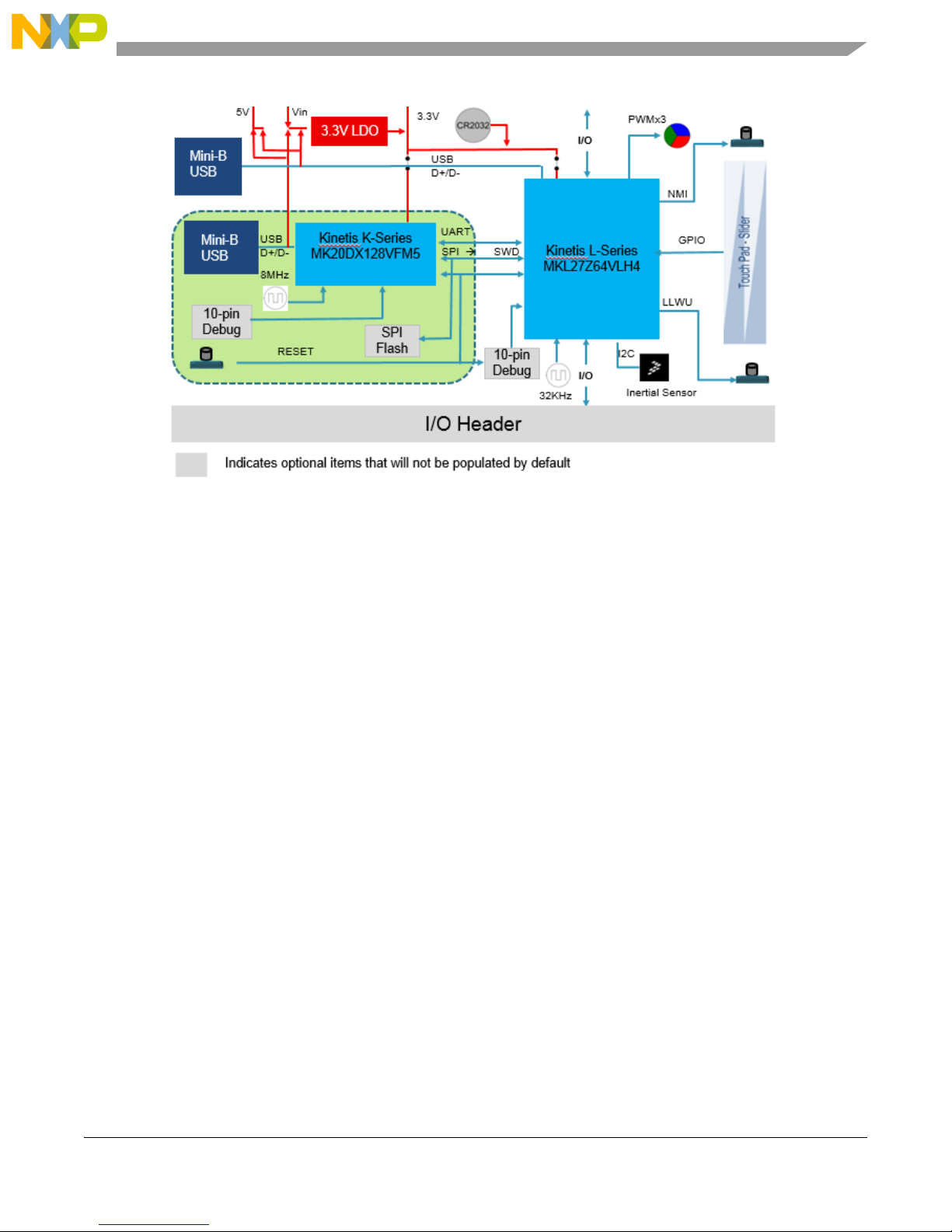
Figure 1. FRDM-KL27Z block diagram
FRDM-KL27Z hardware overview
The FRDM-KL27Z features two microcontrollers (MCUs): the target MCU and a serial and debug adapter
(OpenSDA) MCU. The target MCU is a Kinetis series KL27 family device, the KL27Z64VLH4. The
OpenSDA MCU is a Kinetis K series K20 family device, the K20DX128VFM5.
Features of the KL27Z64VLH4 target MCU include:
• 32-bit ARM Cortex-M0+ core
— Up to 48 MHz operation
— Single-cycle fast I/O access port
• Memories
— 64 KB flash
— 16 KB SRAM
— 16 KB ROM with build-in bootloader
— 32 bytes regfile
• System integration
— 4-channel DMA controller
— Watchdog
— Low-leakage wakeup unit
— SWD debug interface and Micro Trace Buffer
— Bit Manipulation Engine
•Clocks
— 48 MHz high accuracy internal reference clock
— 8/2 MHz low power internal reference clock
Freescale Semiconductor, Inc. 3
FRDMKL27Z User’s Guide, Rev. 0, 02/2015
Page 4

FRDM-KL27Z hardware description
— 32-40 kHz, or 3-32 MHz crystal oscillator
— 1 kHz LPO clock
• Analog peripherals
— 16-bit SAR ADC with internal voltage reference, up to 17 channels
— High-speed analog comparator containing a 6-bit DAC and programmable reference input
— 1.2 V voltage reference (Vref)
• Communication peripherals
— USB full-speed slave controller supporting crystal-less recovery
— Two 16-bit SPI modules
— One UART module supporting ISO7816
— Two LPUART modules
—Two I2C modules supporting up to 1 Mbit/s
— One FlexIO module
•Timers
— One 6-channel Timer/PWM module
— Two 2-channel Timer/PWM modules
— One low-power timer
— Periodic interrupt timer
— Real-time clock
• Security
— 80-bit unique identification number per chip
• Human-Machine Interfaces (HMI)
— Up to 54 general purpose input/output (GPIO)
— GPIO interrupt
— External input pin for LLWU in LLS and VLLSx mode
5 FRDM-KL27Z hardware description
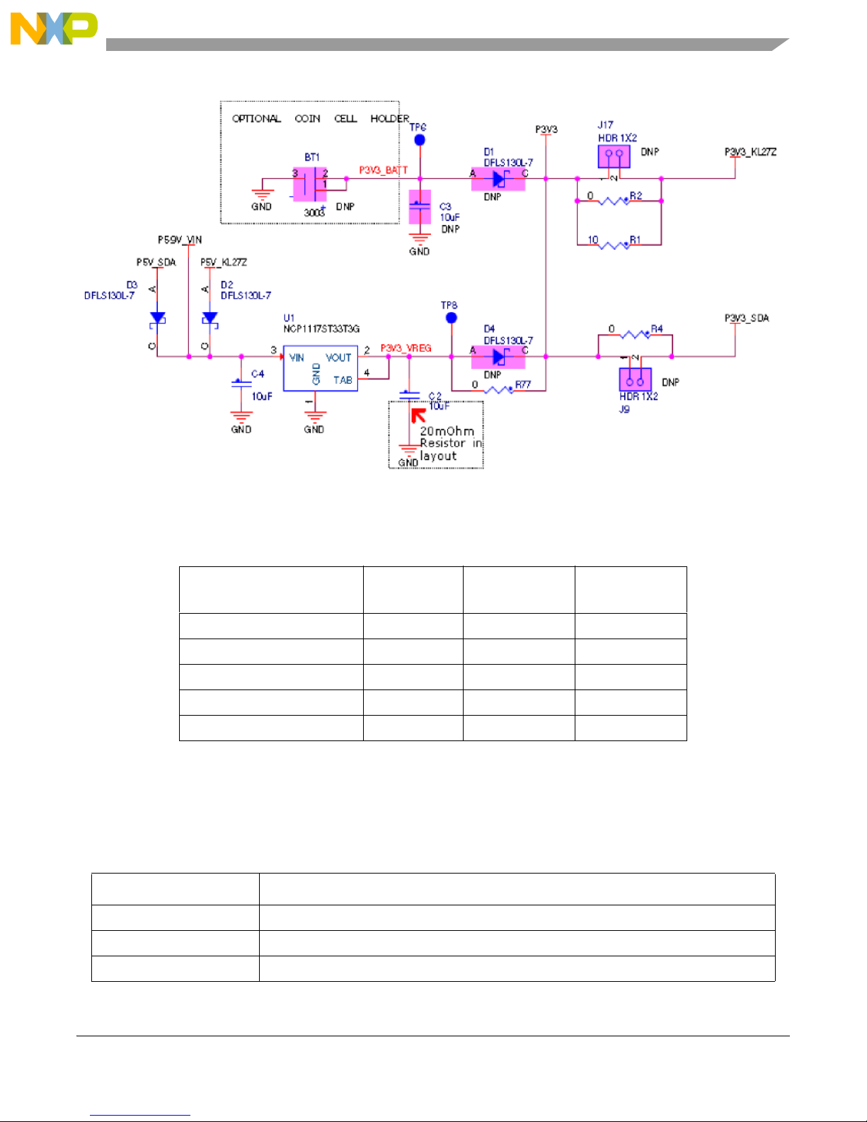
5.1 Power supply
The FRDM-KL27Z offers a design with multiple power supply options. It can be powered from the USB
connector, battery on the board, the VIN pin on the I/O header, or an off-board 1.71-3.6V supply from the
3.3V pin on the I/O header. The USB and VIN supplies are regulated on-board using a 3.3V linear
regulator to produce the main power supply. The other two sources are not regulated on-board. Figure 2
shows the schematic drawing for the power supply inputs and the on-board voltage regulator.
4 Freescale Semiconductor, Inc.
FRDMKL27Z User’s Guide, Rev. 0, 02/2015
Page 5
FRDM-KL27Z hardware description
Figure 2. FRDM-KL27Z power supply
Table 1 provides the operational details and requirements for the power supplies.
Table 1. Tower supply requirements
Supply Source Valid Range
OpenSDA USB (J13) 5V Yes Yes
Mini USB(J10) 5V No Yes
P5V0-9V0_VIN Pin on I/O header 4.3-9V No Yes
P3V3 Pin on I/O header 1.71-3.6V No No
Battery 2-3.6V No No
OpenSDA
Operational?
Regulated
On-board?
NOTE
The OpenSDA circuit is only operational when a USB cable is connected
and supplying power to J13. However, the protection circuitry is in place to
allow multiple sources to be powered at once.
Table 2. FRDM-KL27Z power supplies
Power Supply Name Description
P5V0-9V0_VIN Power supplied from the V
P5V_SDA Power supplied from the OpenSDA USB connector (J13).
P5V_KL27Z Power supplied from the Mini USB connector (J10).
Freescale Semiconductor, Inc. 5
pin of the I/O headers (J3 pin 16).
IN
FRDMKL27Z User’s Guide, Rev. 0, 02/2015
Page 6
FRDM-KL27Z hardware description
Table 2. FRDM-KL27Z power supplies
P3V3_VREG Regulated 3.3V supply. Sources power to the P3V3 supply rail through an optional back drive
protection Schottky diode.
P3V3 Main supply rail for the FRDM-KL27Z. Can be sourced from P3V3_VREG.
P3V3_KL27Z KL27Z MCU power supply. Header J17 provides a convenient means for KL27Z energy consumption
measurements.
P3V3_SDA OpenSDA circuit power supply.
NOTES
J9 and J17 are not populated by default. The two pins of these headers are
in parallel with 0 Ω resistors. In addition, J17 is also in parallel with a 10 Ω
resistor. To measure the energy consumption of the KL27Z, either a
voltmeter or an ammeter may be used. To use a voltmeter, R2 (0 Ω) must be
removed before connecting the voltmeter probes to the pins of J17. Both R1
and R2 (10 Ω) must be removed to measure current with an ammeter. For
the OpenSDA MCU, energy consumption can be measured by removing R4
(0 Ω) and connecting ammeter probes to the pins of J9.
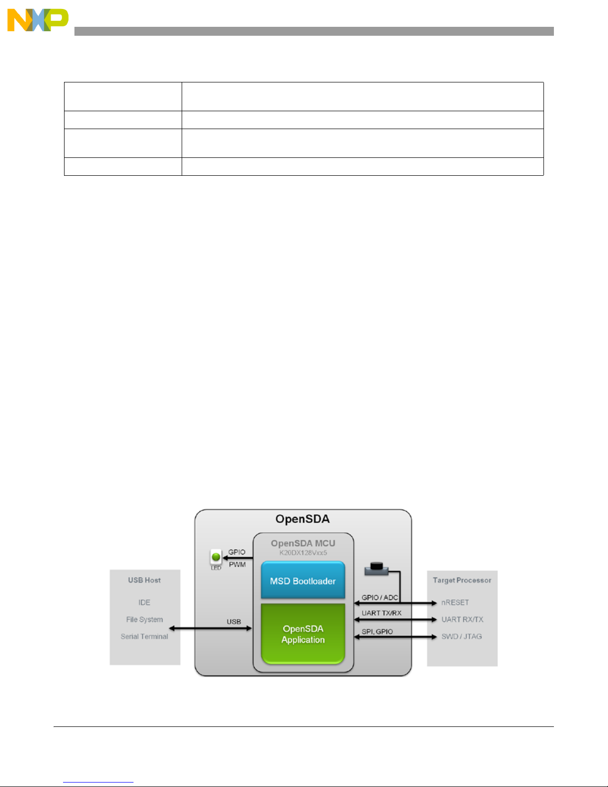
5.2 Serial and debug adapter (OpenSDA)
OpenSDA is an open-standard serial and debug adapter. It bridges serial and debug communications
between a USB host and an embedded target processor as shown in Figure 3. The hardware circuit is
based on a Freescale Kinetis K20 family MCU with 128 KB of embedded flash and an integrated USB
controller. OpenSDA features a mass storage device (MSD) bootloader, which provides a quick and easy
mechanism for loading different OpenSDA Applications such as flash programmers, run-control debug
interfaces, serial-to-USB converters, and more. Two or more OpenSDA applications can run simultaneously. For example, run-control debug application and serial-to-USB converter runs in parallel to provide a virtual COM communication interface while allowing code debugging via OpenSDA with just a
single USB connection. These two applications are provided in a single code package. Refer to the
OpenSDA User’s Guide for more details.
6 Freescale Semiconductor, Inc.
Figure 3. OpenSDA block diagram
FRDMKL27Z User’s Guide, Rev. 0, 02/2015
Page 7
FRDM-KL27Z hardware description
OpenSDA is managed by a Kinetis K20 MCU built on the ARM Cortex-M4 core. The OpenSDA circuit
includes a status LED (D8) and a RESET pushbutton (SW2). The pushbutton asserts the Reset signal to
the KL27Z target MCU. It can also be used to place the OpenSDA circuit into Bootloader mode by holding
down the RESET pushbutton while plugging the USB cable to USB connector J13. Once the OpenSDA
enters bootloader mode, other OpenSDA applications such as debug app can be programmed.
SPI and GPIO signals provide an interface to the SWD debug port of the KL27Z. Additionally, signal
connections are available to implement a UART serial channel. The OpenSDA circuit receives power
when the USB connector J13 is plugged into a USB host.
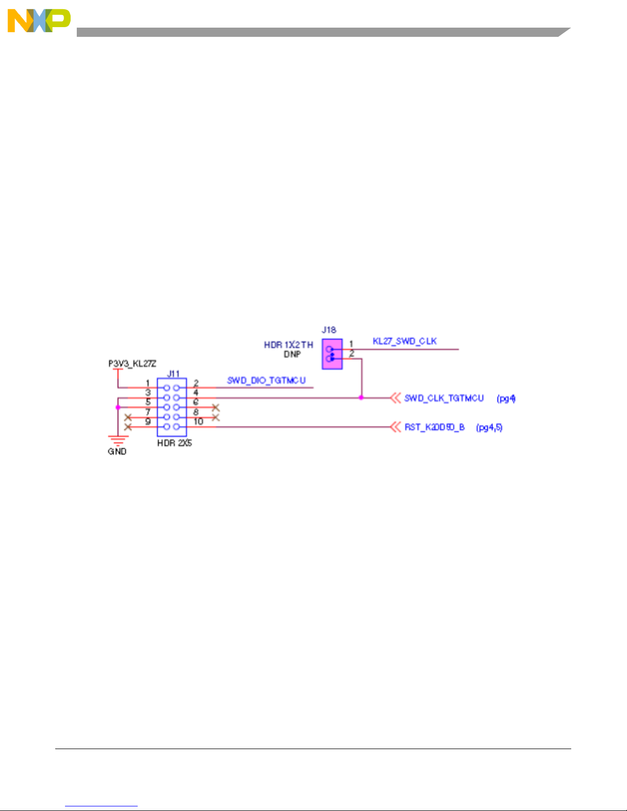
5.3 Debugging interface
Signals with SPI and GPIO capability are used to connect directly to the SWD of the KL27Z. These signals
are also brought out to a standard 10-pin (0.05”) Cortex Debug connector (J11) as shown in Figure 4. It is
possible to isolate the KL27Z MCU from the OpenSDA circuit and use J11 to connect to an off-board
MCU. To accomplish this, cut the trace between pin1 and pin2 of J18 on bottom layer. This will disconnect
the SWD_CLK pin to the KL27Z so that it will interfere with the communications to an off-board MCU
connected to J11.
Figure 4. SWD debug connector to KL27Z
5.4 Virtual serial port
A serial port connection is available between the OpenSDA MCU and LPUART0 pin PTA1(TXD) and
PTA2 (RXD) of KL27Z. Several of the default OpenSDA Applications provided by Freescale, including
the MSD Flash Programmer and the P&E Debug Application, provide a USB Communications Device
Class (CDC) interface that bridges serial communications between the USB host and this serial interface
on the KL27Z.
5.5 Clock source
The Kinetis KL27 microcontrollers feature an on-chip oscillator compatible with input crystal: 32 to 40
KHz or 3 to 32 MHz. The KL27Z on the FRDM-KL27Z is clocked from the internal clock LIRC (2 MHz/8
MHz) or HIRC (48 MHz), and on-board 32768 Hz crystal for the RTC clock source.
FRDMKL27Z User’s Guide, Rev. 0, 02/2015
Freescale Semiconductor, Inc. 7
Page 8

FRDM-KL27Z hardware description
5.6 Serial port
The serial port interface signals used with OpenSDA are LPUART0 pin PTA1 (TXD) and PTA2 (RXD).
These signals are also connected to I/O header J1.
5.7 Reset
The RESET signal on the KL27Z is connected externally to a pushbutton, SW2. The reset button can be
used to force an external reset event in the target MCU. The reset button can also be used to force the
OpenSDA circuit into bootloader mode when plugging the USB cable to J13. Refer to Section 5.2, “Serial
and debug adapter (OpenSDA)” for more details.
5.8 Debug
The sole debug interface on all Kinetis L series devices is a Serial Wire Debug (SWD) port. The primary
controller of this interface on the FRDM-KL27Z is the onboard OpenSDA circuit. However, a 2x5-pin
(0.05”) Cortex Debug connector, J11, provides access to the SWD signals for the KL27Z MCU. Ta ble 3
shows SWD connector signals description for KL27Z.
Table 3. ARM JTAG/SWD mini connector description
Pin Function Connection to KL27Z
1 VTref P3V3_MCU
2 SWDIO/TMS PTA3
3GND GND
4SWDCLK/TCK PTA0
5GND GND
6 SWO/TDO NC
7NC NC
8 TDI NC
9NC NC
10 RESET PTA20
5.9 Capacitive touch slider
Two GPIO pins functioning as Touch Sense Input (TSI) signals, are connected to capacitive electrodes
configured as a touch slider as shown in Figure 5.
8 Freescale Semiconductor, Inc.
FRDMKL27Z User’s Guide, Rev. 0, 02/2015
Page 9

FRDM-KL27Z hardware description
Figure 5. Touch slider connection
5.10 6-axis accelerometer and magnetometer
A Freescale MMA8451Q low-power, three-axis accelerometer is interfaced through an I2C bus and two
GPIO signals as shown in Table 4. By default, the I2C address is 0x1D (SA0 pulled high).
Table 4. Accelerometer signal connections
MMA8451Q KL27Z
SCL PTD7
SDA PTD6
INT1 PTC3
INT2 PTC2
Freescale Semiconductor, Inc. 9
Figure 6. Accelerometer connection
FRDMKL27Z User’s Guide, Rev. 0, 02/2015
Page 10

FRDM-KL27Z hardware description
This also designed to be compatible with 6-axis (FXOS8700CQ) combination of accelerometer and
magnetometer sensor, if populating the U10 (FXOS8700CQ), and then keep U2 (MAG3310) DNP.
Otherwise, populate U10 (MMA8451) and U2 (MAG3110).
A Freescale MAG3110 low-power, three-axis magnetometer is interfaced through an I2C bus and one
2
GPIO signals as shown in Table 5. By default, the I
Table 5. Magnetometer signal connections
MMA8451Q KL27Z
SCL PTD7
SDA PTD6
INT1 PTC2
C address is 0x0E .
Figure 7. Magnetometer connection
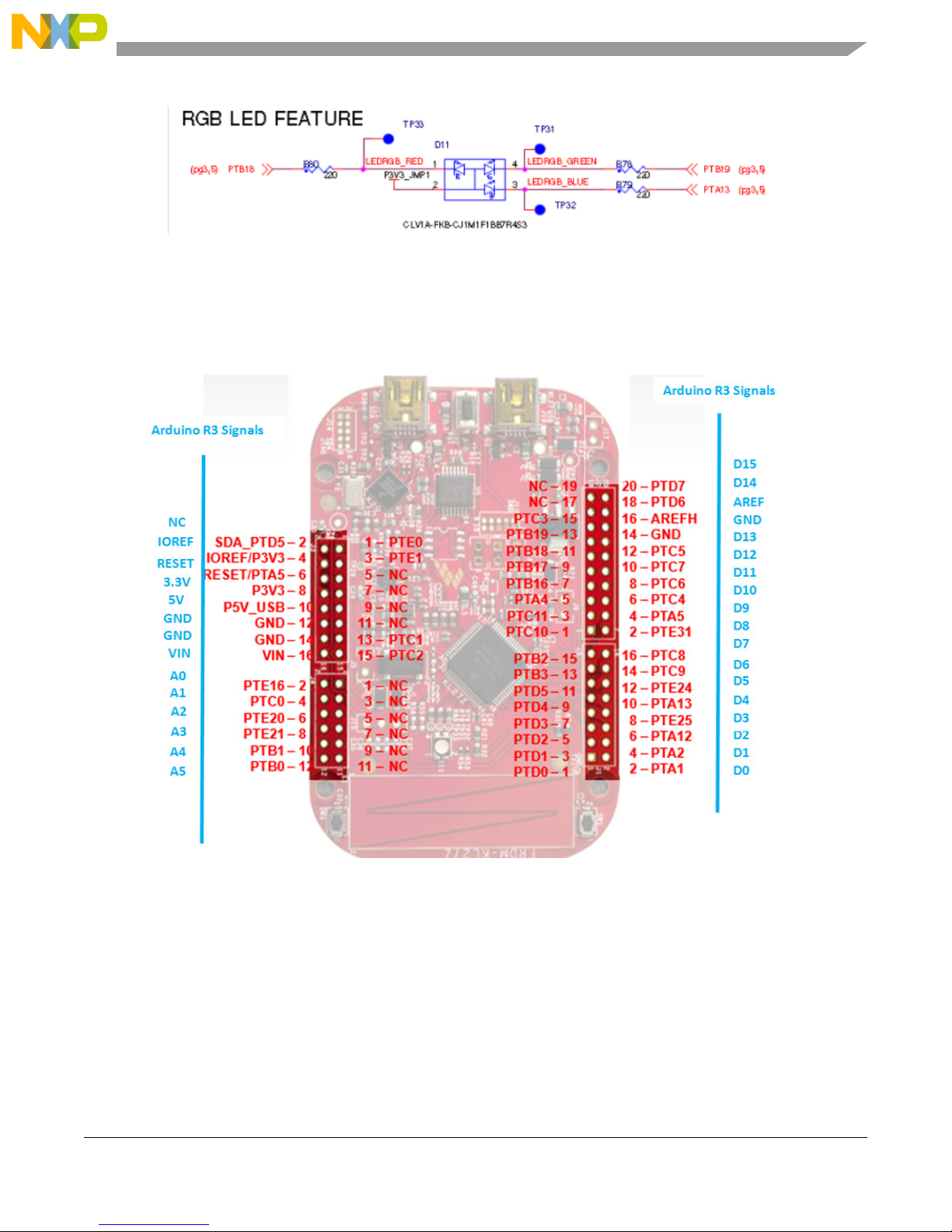
5.11 RGB LED
Three PWM-capable KL27Z signals are connected to a red, green, and blue LED. The signal connections
are shown in Table 6.
Table 6. RGB LED signal connections
RGB LED KL27Z
Red Cathode PTB18
Green Cathode PTB19
Blue Cathode PTA13
FRDMKL27Z User’s Guide, Rev. 0, 02/2015
10 Freescale Semiconductor, Inc.
Page 11
FRDM-KL27Z hardware description
Figure 8. RGB LED connection
5.12 Input/output headers
The MKL27Z64VLH4 MCU is packaged in a 64-pin LQFP. Some pins are utilized by on-board circuitry,
but many are directly connected to one of four I/O headers (J1, J2, J3 and J4).
5.13 Arduino compatibility
The I/O headers on the FRDM-KL27Z are arranged to allow compatibility with peripheral boards (known
as shields) that connect to Arduino and Arduino-compatible MCU boards. The pins on the headers share
the same mechanical spacing and placement as the I/O headers on the Arduino Uno Revision 3 board
design. See Figure 9 for compatible signals.
Freescale Semiconductor, Inc. 11
Figure 9. I/O headers
FRDMKL27Z User’s Guide, Rev. 0, 02/2015
Page 12

Using the FRDM-KL27Z with EEMBC ULPBench
6 Using the FRDM-KL27Z with EEMBC ULPBench
The FRDM-KL27Z board supports the EEMBC® ULPBench benchmark. Information on this benchmark,
including a description of what it is and instructions on how to obtain and use the associated
EnergyMonitor hardware and software can be found at EEMBC.org.
The FRDM-KL27Z board can easily be modified to support the EEMBC ULPBench benchmark and the
connection of the EEMBC EnergyMonitor v1.0.
6.1 Hardware modifications required for EnergyMonitor
The only board modifications required are to configure the board to measure current and isolate the
OpenSDA MCU (refer to Figure 2).
• Add J17 and remove R1 and R2. This provides a means of powering the KL27 Kinetis MCU with
the EnergyMonitor.
• Add J9 and remove R4 to isolate the OpenSDA MCU Vdd supply.
• Remove R7, R21 and R83 to isolate external current paths.
• Add a single pin header to TP4.
6.2 Programming the ULPBench device software
The ULPBench requires that the specific ULPBench profile software be loaded on the target device. This
can be performed by either using the on-board OpenSDA debug/MSD interface, instruction for which can
be found in the OpenSDA User’s Guide, or by means of an external SWD interface (J11 would need to be
populated to use this method). If the default on-board interface is being used then J5, J6, J7, J9 and J17
must be placed while the code is programmed into the KL27 device. The board should be powered by
means of USB connector J3 when programming the KL27. The EnergyMonitor should not be used to
power the board when programming the KL27. These jumpers, along with the USB cable, must be
removed when the EnergyMonitor is running to obtain the correct benchmark score.
6.3 Hardware configuration
The KL27 must be isolated from the OpenSDA MCU and any external pull up devices which may draw
additional current. The hardware modifications in Section 6.1, “Hardware modifications required for
EnergyMonitor” must first be made. The following board jumpers must be removed:
• J9 and J17 to isolate the power supply and allow connection of the EnergyMonitor
• J5 to isolate the RESET line from the OpenSDA MCU
• J6 and J7 to isolate the SWD signals from the OpenSDA MCU
• J19 and J22 to isolate several external pull up devices
• J23 and J24 to isolate the I2C signals from the on board sensor devices
• J25 and J26 to isolate the UART signals from the OpenSDA MCU
• J27 and J28 to isolate the interrupt signals from the on board sensor devices
12 Freescale Semiconductor, Inc.
FRDMKL27Z User’s Guide, Rev. 0, 02/2015
Page 13

Revision history
6.4 EnergyMonitor connections
The EnergyMonitor Vcc line should be connected to J17 pin2 and the EnergyMonitor GND line should be
connected to TP4.
7 Revision history
This table provides a revision history for this document.
Table 7. Revision history
Rev.
number
1 02/2015 Initial public release.
Date Substantive change(s)
Freescale Semiconductor, Inc. 13
FRDMKL27Z User’s Guide, Rev. 0, 02/2015
Page 14

How to Reach Us:
Home Page:
freescale.com
Web Support:
freescale.com/support
Information in this document is provided solely to enable system and software
implementers to use Freescale products. There are no express or implied copyright
licenses granted hereunder to design or fabricate any integrated circuits based on the
information in this document.
Freescale reserves the right to make changes without further notice to any products
herein. Freescale makes no warranty, representation, or guarantee regarding the
suitability of its products for any particular purpose, nor does Freescale assume any
liability arising out of the application or use of any product or circuit, and specifically
disclaims any and all liability, including without limitation consequential or incidental
damages. “Typical” parameters that may be provided in Freescale data sheets and/or
specifications can and do vary in different applications, and actual performance may
vary over time. All operating parameters, including “typicals,” must be validated for
each customer application by customer’s technical experts. Freescale does not convey
any license under its patent rights nor the rights of others. Freescale sells products
pursuant to standard terms and conditions of sale, which can be found at the following
address: freescale.com/SalesTermsandConditions.
Freescale, the Freescale logo, and Kinetis are trademarks of Freescale
Semiconductor, Inc., Reg. U.S. Pat. & Tm. Off. All other product or service names are
the property of their respective owners. ARM and ARM Cortex are the registered
trademarks of ARM Limited (or its subsidiaries) in the EU and/or elsewhere. All rights
reserved.
© 2015 Freescale Semiconductor, Inc.
Document Number: FRDMKL27ZUG
Rev. 0
02/2015
 Loading...