

Page 1
Freescale Semiconductor, Inc.
© Freescale Semiconductor, Inc., 2013. All rights reserved.
User’s Guide
Document Number: KTXSWITCH4UG
Rev. 1.0, 11/2013
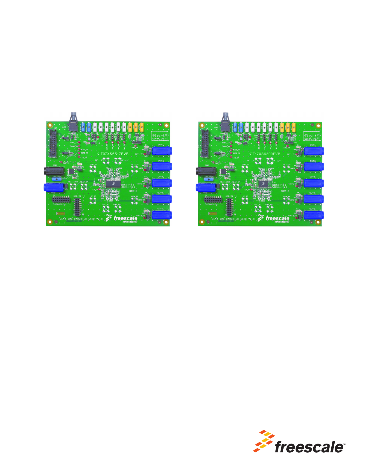
eXtreme Switch Gen4 Evaluation Board
Featuring the MC07XS6517 and MC17XS6500 Penta High Side Switch
Figure 1. eXtreme Switch Gen4 Evaluation Boards
Contents
1 Kit Contents/Packing List . . . . . . . . . . . . . . . . . . . . . . . . . . . . . . . . . . . . . . . . . . . . . . . . . . . . . . . . . . . . . . . 2
2 Jump Start . . . . . . . . . . . . . . . . . . . . . . . . . . . . . . . . . . . . . . . . . . . . . . . . . . . . . . . . . . . . . . . . . . . . . . . . . . 2
3 Important Notice. . . . . . . . . . . . . . . . . . . . . . . . . . . . . . . . . . . . . . . . . . . . . . . . . . . . . . . . . . . . . . . . . . . . . . 3
4 Introduction . . . . . . . . . . . . . . . . . . . . . . . . . . . . . . . . . . . . . . . . . . . . . . . . . . . . . . . . . . . . . . . . . . . . . . . . . 4
5 Evaluation Board Features . . . . . . . . . . . . . . . . . . . . . . . . . . . . . . . . . . . . . . . . . . . . . . . . . . . . . . . . . . . . . 4
6 MC07XS6517 and MC17XS6500 Device Features . . . . . . . . . . . . . . . . . . . . . . . . . . . . . . . . . . . . . . . . . . .4
7 Accessory Interface Board. . . . . . . . . . . . . . . . . . . . . . . . . . . . . . . . . . . . . . . . . . . . . . . . . . . . . . . . . . . . . . 5
8 Required Equipment . . . . . . . . . . . . . . . . . . . . . . . . . . . . . . . . . . . . . . . . . . . . . . . . . . . . . . . . . . . . . . . . . . 5
9 Evaluation Board Configuration . . . . . . . . . . . . . . . . . . . . . . . . . . . . . . . . . . . . . . . . . . . . . . . . . . . . . . . . . . 6
10 Installing SPIGen Freeware on your Computer . . . . . . . . . . . . . . . . . . . . . . . . . . . . . . . . . . . . . . . . . . . . . 7
11 Setting Up and Using the Hardware . . . . . . . . . . . . . . . . . . . . . . . . . . . . . . . . . . . . . . . . . . . . . . . . . . . . . 8
12 Evaluation Board Hardware Description . . . . . . . . . . . . . . . . . . . . . . . . . . . . . . . . . . . . . . . . . . . . . . . . . . 9
13 Schematic . . . . . . . . . . . . . . . . . . . . . . . . . . . . . . . . . . . . . . . . . . . . . . . . . . . . . . . . . . . . . . . . . . . . . . . . 13
14 Board Layout . . . . . . . . . . . . . . . . . . . . . . . . . . . . . . . . . . . . . . . . . . . . . . . . . . . . . . . . . . . . . . . . . . . . . . 15
15 Bill of Material . . . . . . . . . . . . . . . . . . . . . . . . . . . . . . . . . . . . . . . . . . . . . . . . . . . . . . . . . . . . . . . . . . . . . 21
16 References. . . . . . . . . . . . . . . . . . . . . . . . . . . . . . . . . . . . . . . . . . . . . . . . . . . . . . . . . . . . . . . . . . . . . . . . 23
17 Revision History . . . . . . . . . . . . . . . . . . . . . . . . . . . . . . . . . . . . . . . . . . . . . . . . . . . . . . . . . . . . . . . . . . . . 24
Page 2

Kit Contents/Packing List
Jump Start Your Design
1 Kit Contents/Packing List
• Assembled and tested evaluation board/module in anti-static bag.
• Warranty card
2Jump Start
•Go to www.freescale.com/analogtools
• Locate your kit
• Review your Tool Summary Page
• Look for
• Download documents, software and other information
2 Freescale Semiconductor, Inc.
KTXSWITCH4UG User’s Guide Rev. 1.0 11/2013
Page 3

3 Important Notice
Freescale provides the enclosed product(s) under the following conditions:
This evaluation kit is intended for use of ENGINEERING DEVELOPMENT OR EVALUATION PURPOSES
ONLY. It is provided as a sample IC pre-soldered to a printed circuit board to make it easier to access inputs,
outputs, and supply terminals. This evaluation board may be used with any development system or other
source of I/O signals by simply connecting it to the host MCU or computer board via off-the-shelf cables. This
evaluation board is not a Reference Design and is not intended to represent a final design recommendation
for any particular application. Final device in an application will be heavily dependent on proper printed circuit
board layout and heat sinking design as well as attention to supply filtering, transient suppression, and I/O
signal quality.
The goods provided may not be complete in terms of required design, marketing, and or manufacturing related
protective considerations, including product safety measures typically found in the end product incorporating
the goods. Due to the open construction of the product, it is the user's responsibility to take any and all
appropriate precautions with regard to electrostatic discharge. In order to minimize risks associated with the
customers applications, adequate design and operating safeguards must be provided by the customer to
minimize inherent or procedural hazards. For any safety concerns, contact Freescale sales and technical
support services.
Should this evaluation kit not meet the specifications indicated in the kit, it may be returned within 30 days from
the date of delivery and will be replaced by a new kit.
Freescale reserves the right to make changes without further notice to any products herein. Freescale makes
no warranty, representation or guarantee regarding the suitability of its products for any particular purpose, nor
does Freescale assume any liability arising out of the application or use of any product or circuit, and
specifically disclaims any and all liability, including without limitation consequential or incidental damages.
“Typical” parameters can and do vary in different applications and actual performance may vary over time. All
operating parameters, including “Typical”, must be validated for each customer application by customer’s
technical experts.
Freescale does not convey any license under its patent rights nor the rights of others. Freescale products are
not designed, intended, or authorized for use as components in systems intended for surgical implant into the
body, or other applications intended to support or sustain life, or for any other application in which the failure
of the Freescale product could create a situation where personal injury or death may occur.
Should Buyer purchase or use Freescale products for any such unintended or unauthorized application, Buyer
shall indemnify and hold Freescale and its officers, employees, subsidiaries, affiliates, and distributors
harmless against all claims, costs, damages, and expenses, and reasonable attorney fees arising out of,
directly or indirectly, any claim of personal injury or death associated with such unintended or unauthorized
use, even if such claim alleges that Freescale was negligent regarding the design or manufacture of the
part.Freescale™ and the Freescale logo are trademarks of Freescale Semiconductor, Inc. All other product or
service names are the property of their respective owners.
© Freescale Semiconductor, Inc. 2013
Important Notice
Freescale Semiconductor, Inc. 3
KTXSWITCH4UG User’s Guide Rev. 1.0 11/2013
Page 4

Introduction
4 Introduction
This evaluation board demonstrates the capability of the latest eXtreme Switch Gen4 family. This family offers
new combinations of output channels as well as a selection of Rdson values. All devices are
footprint-compatible; therefore, they can all be evaluated using this evaluation board.
This evaluation board can be used to evaluate either the MC07XS6517 or the MC17XS6500 which are both
12
V penta high side devices that feature integrated control with high flexibility, and high number of protection
and diagnostic functions. These devices are designed for low-voltage automotive lighting applications and can
drive a wide range of sources, including HIB ballasts and LEDs.
Programming, control and diagnostics are accomplished using a 16-bit SPI interface, which makes possible a
large array of configurations, diagnostics and protection features. For example, see below:
• Configuration: Output slew rates, PWM frequency with prescaler, output phasing, current sense precision,
etc.
• Protection and diagnostics: under/overvoltage, thermal warning, overcurrent, open load, SPI fail, etc.
These devices also provide analog feedback of the IC's temperature, battery voltage or selectable-channel
current sensing with high precision.
The five channels can be controlled individually by external clock signal or in fail safe mode by using direct inputs
(available for OUT1 through OUT4). This fail-safe mode operation happens whenever communication with the
external microcontroller is lost (due to watchdog time-out) and all protection as well as control remains
operational.
5 Evaluation Board Features
This evaluation board consists of either an MC07XS6517 or MC17XS6500 IC in SOIC 54 or 32 pins with
exposed pads.
This board can control
• Five separate 28 W bulbs
• Three separate 55 W HID ballasts
• Five separate LED modules
• Five separate loads of other types
Device can be driven by the 16-bit SPI using KITUSBSPI with SPIGen software or with direct input signals in
Fail safe mode operation. It also offers the possibility to apply an external clock in order to drive outputs in PWM
operation.
6 MC07XS6517 and MC17XS6500 Device Features
MC07XS6517 and MC17XS6500 are smart + power ICs intended for lighting application. The devices supports
the following functions:
• Five protected high side switches
–3*7 mOhms + 2*17 mOhms for the MC07XS6517
–5*17 mOhms for the MC17XS6500
• Operating voltage range from 6.0 V to 18 V with sleep current < 5.0 µA.
• 16-bit 5.0 V SPI control, programming and status reporting with daisy chain capability
• PWM module using external clock with programmable slew rates (to satisfy EMC requirements), 8-bit
flexibility for duty cycle and output delay management.
• Smart overcurrent shutdown, severe short circuit detection, overtemperature protections, output short to
battery, undervoltage or overvoltage reporting, etc.
• Open load detection in On or Off state, available for bulbs and LEDs
• Analog temperature and voltage feedback, so current with selectable ratio is optimized for LEDs modules
4 Freescale Semiconductor, Inc.
KTXSWITCH4UG User’s Guide Rev. 1.0 11/2013
Page 5
Freescale analog ICs are manufactured using the SMARTMOS process, a combinational BiCMOS
manufacturing flow that integrates precision analog, power functions and dense CMOS logic together on a
single cost-effective die. All power channels are integrated using LFet45V technology.
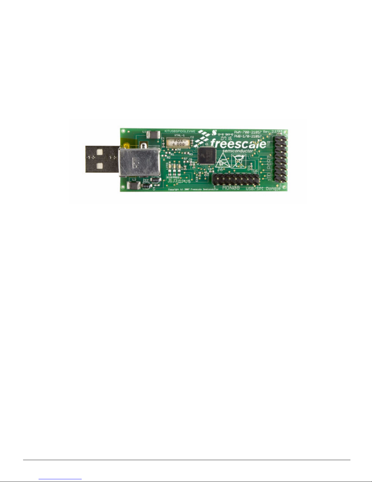
7 Accessory Interface Board
The eXtreme Switch Gen4 Evaluation board may be used with the KITUSBSPIDGLEVME interface dongle
(shown below), which provides a USB-to-SPI interface. This small board makes use of the USB and SPI ports
built into Freescale’s MC68HC908JW32 microcontroller. The main function provided by this dongle is to allow
Freescale evaluation boards that have an SPI port to communicate with a PC through its USB port.
Accessory Interface Board
Figure 2. KITUSBSPIDGLEVME Interface Dongle
8 Required Equipment
Minimum equipment required:
• Minimum equipment required for optimal use:
• DC Power supply 30 V/40 A
• Clock signal generator 0-100 kHz
• Computer with an available USB port, running Windows XP or higher
• KITUSBSPIDGLEVME interface board
• Latest version of SPIGen software (available through www.freescale.com/analogtools)
• Typical loads (lamps)
Freescale Semiconductor, Inc. 5
KTXSWITCH4UG User’s Guide Rev. 1.0 11/2013
Page 6
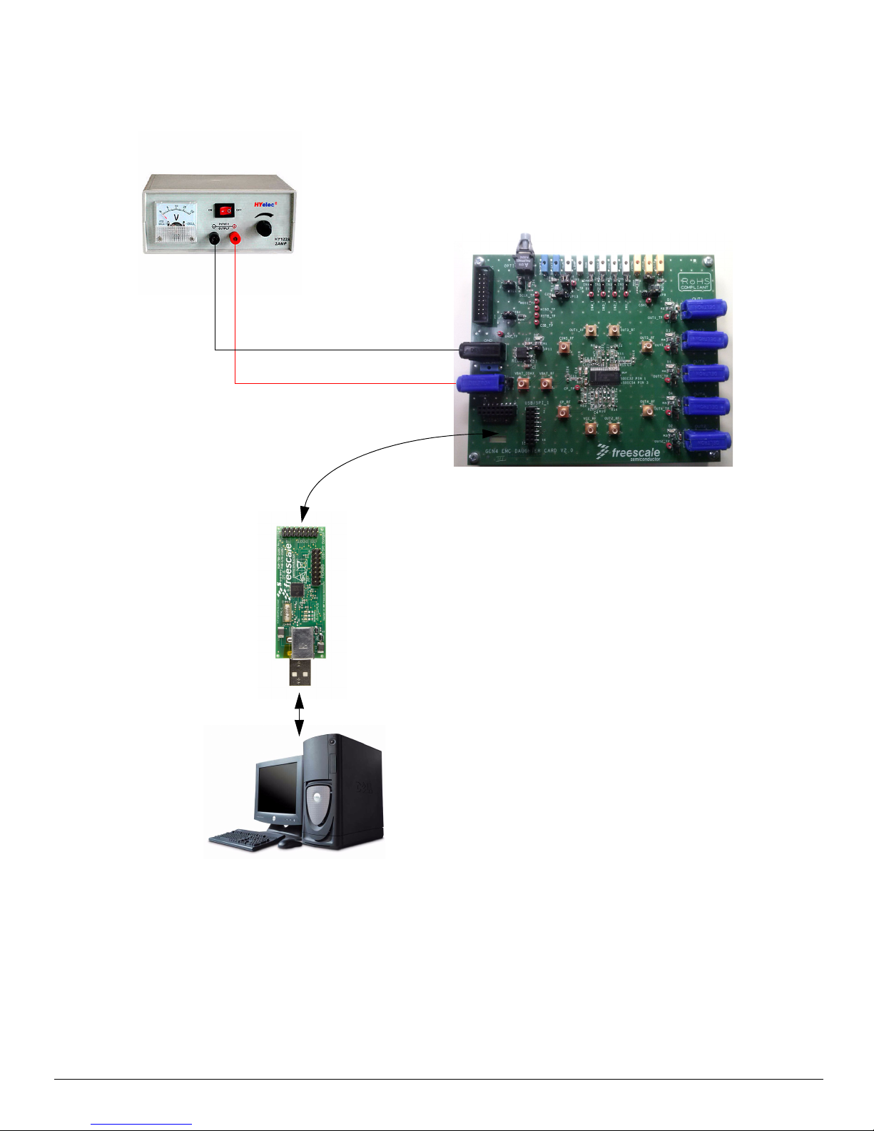
Evaluation Board Configuration
GND
+12 V
eXtreme Switch Gen4
Evaluation Board
USB/SPI Dongle
(KITUSBSPIDGLEVME)
16-Pin SPI Ribbon
Cable
Power Supply
9 Evaluation Board Configuration
Figure 3. eXtreme Switch Gen4 Evaluation Board plus KITUSBSPIDGLEVME Board Setup
6 Freescale Semiconductor, Inc.
KTXSWITCH4UG User’s Guide Rev. 1.0 11/2013
Page 7
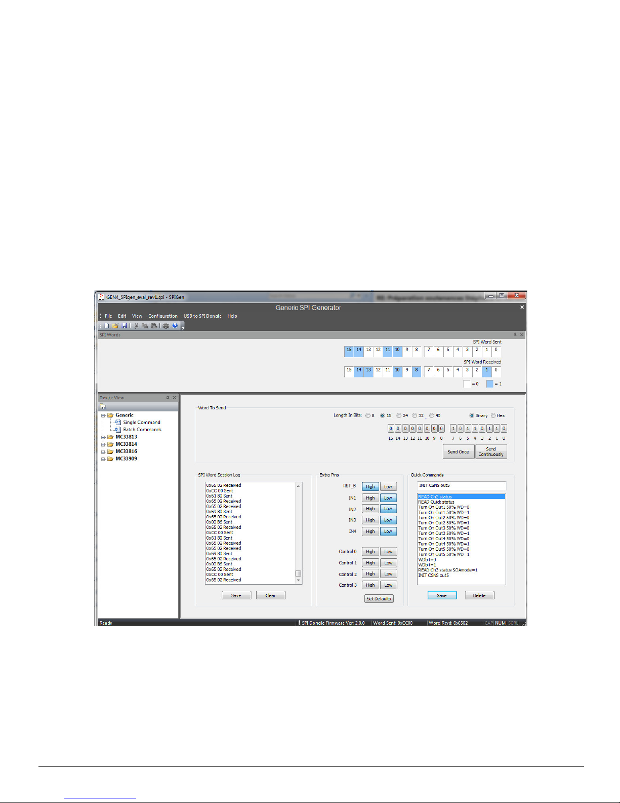
Installing SPIGen Freeware on your Computer
10 Installing SPIGen Freeware on your Computer
The latest version of SPIGen is designed to run on any Windows 8, Windows 7, Vista or XP-based operating
system. To install the software, go to
open the corresponding Tool Summary Page. Look for “Jump Start Your Design”. Download to your computer
desktop the SPIGen software as well as the associated configuration file.
Run the install program from the desktop. The Installation Wizard will guide you through the rest of the process.
To use SPIGen, go to the Windows Start menu, then Programs, then SPIGen, and click on the SPIGen icon.
The SPIGen Graphic User Interface (GUI) will appear. Go to the file menu in the upper left hand corner of the
GUI, and select “Open”. In the file selection window that appears, set the “Files of type:” drop-down menu to
“SPIGen Files (*.spi)”. (As an exceptional case, the file name may have a .txt extension, in which case you
should set the menu to “All Files (*.*)”.) Next, browse for the configuration file you saved on your desktop earlier
and select it. Click “Open”, and SPIGen will create a specially configured SPI command generator for your
evaluation board.
The GUI is shown in Figure 4. The text at the top is the name of the configuration file loaded. The left side panel
displays folders that group user interfaces. The process of loading the configuration file has assigned a list of
“Extra Pins” as well as a list “Quick Commands”, all of which are board-specific.
www.freescale.com/analogtools and select your kit. Click on that link to
Freescale Semiconductor, Inc. 7
Figure 4. SPIGen GUI
KTXSWITCH4UG User’s Guide Rev. 1.0 11/2013
Page 8

Setting Up and Using the Hardware
11 Setting Up and Using the Hardware
In order to perform the demonstration examples, first set up the evaluation board hardware and software as
follows:
1. Ready the computer and install the latest available version of SPIGen GUI. Then connect the cable
between this interface board and computer. Finally, plug this interface board into the eXtreme Switch Gen4
Evaluation Board.
2. Attach a DC power supply (without turning on the power) to evaluation board’s Vpwr-Gnd connectors and
attach loads to the KIT07XS6517EVBE board. Plug the USB/SPI interface dongle (KITUSBSPIDGLEVME)
directly into the evaluation board.
3. Use as many output terminals as desired.
4. Launch SPIGen and load the GEN4_SPIgen_eval_rev1.spi configuration file obtained from the Jump Start
download.
5. Turn on the power supply with the correct voltage and verify that EVB is supplied correctly by observing the
D6 LEDs with JP1 and JP11 closed. J1 and J7 have to be set either to the Vcc or the µC position. Set all
the LED jumpers, JP2 to JP6, to outputs pins; set the "Extra Pin" RST_B (if J1 in uC position) to high on
the SPIGen GUI and then do the following verification:
6. Click on the "Extra Pins" button INx. The corresponding OUTx LED should turn on.
7. Click on the "Send Once" button. The 'SPI Word Received' at the top of the screen should answer
something different from 0x0000.
Once the steps above are all accomplished, then you are ready to proceed with the remaining examples.
11.1 SPIGen Software information
On the left side of the "device view", you have two options:
• "Single Command": The screen displays 16 bits from the SP interface, so the user can configure them easily
in binary or hexadecimal. You will also find at the top, the corresponding status of SI and SO bits and on
bottom left, the "SPI Word Session Log". Extra pins are also available for configuration.
• "Batch Commands" allows the user to create a specific function using commands that already exist.
Note:
• Some commands and batches of commands are already set up in the GEN4_SPIgen_eval_rev1.spi file.
You may create and save your own command for specific purposes.
• Gen4 devices need a WD toggle on bit D11 to stay in normal mode. The interface board
KITUSBSPIDGLEVME is not able to generate and take into account WD bit status. Therefore, when doing
your own sequence, you may take this into account, and use the "Send Continuously" button.
8 Freescale Semiconductor, Inc.
KTXSWITCH4UG User’s Guide Rev. 1.0 11/2013
Page 9

Evaluation Board Hardware Description
Device Under Test
Add SOIC32 pin 1 marking:
corresponds to pin3 of SOIC54
Capacitors layout placement:
- C22, C24, C20, C18, C16: near banana
- C23, C25, C21, C19, C17: near DUT pi
- C12, C13, C14, C15: near DUT
AGND
AGND AGND
AGND
AGND
AGND
AGND
AGND
AGND
OUT1
OUT2
OUT3
OUT4
OUT5
OUT6
CSNS
/SYNC
IN4
IN3
IN2
IN1
LIMP
CLK
MISO
MOSI
SCLK
CSB
RSTB
Vcc CP
Vcc
Vbat
C13
0.1UF
R265.0K
DUT
T07D17
IN1
47
IN2
48
IN3
49
IN4
50
CLK
52
LIMP
51
CS
5
SCLK
6
MOSI
7
MISO
9
RST
4
GND_111GND_2
44
VCC
8
CP
3
VBAT
55
OUT1_1
42
OUT1_2
43
OUT2_1
12
OUT2_2
13
OUT3_1
39
OUT3_2
40
OUT3_3
41
OUT4_1
14
OUT4_2
15
OUT4_3
16
OUT5_1
28
OUT5_2
29
OUT5_3
30
OUT5_4
31
OUT5_5
32
OUT5_6
33
OUT5_7
34
OUT5_8
35
OUT5_9
36
OUT5_10
37
OUT5_11
38
OUT6
10
CSNS
45
SYNC
46
NC_1
1
NC_2
2
NC_17
17
NC_18
18
NC_19
19
NC_20
20
NC_21
21
NC_22
22
NC_23
23
NC_24
24
NC_25
25
NC_26
26
NC_27
27
NC_53
53
NC_54
54
C20
0.022UF
JP8
12
C25
1000PF
C21
1000PF
C18
0.022UF
C14
0.1UF
C19
1000PF
C16
0.022UF
C15
1000PF
C17
1000PF
C22
0.022UF
R27
5.0K
C12
0.1UF
C24
0.022UF
C23
1000PF
12 Evaluation Board Hardware Description
This evaluation board has the capability to demonstrate the functionality of either the MC07XS6517 or
17XS6500 IC, when either of those devices is mounted on the board as a Device Under Test. Below are shown
the DUT connections on the board. The labels displayed in red are accessible to a PC running SPIGen software.
12.1 LED Display
The following LEDs are provided as visual output devices for the KIT07XS6517EVBE evaluation board:
1. {LED Dx} indicates when the corresponding Outputx is On
2. {LED D6} indicates that Vcc is supplied by the on-board regulator
12.2 Test Point Definitions
Freescale Semiconductor, Inc. 9
Each test point of the board has a label showing its corresponding signal.
Figure 5. Device Under Test Signals
KTXSWITCH4UG User’s Guide Rev. 1.0 11/2013
Page 10

Evaluation Board Hardware Description
Output power connections
+12V
supply
KITUSBSPIDGLEVME Interface
Dongle
Spare
connector
for μC
Device I/Os
5V
ext
sup
CLK
opt
12.3 Input Signal Definitions
The MC07XS6517 and MC17XS6500 ICs both have special input signals that are used to control certain outputs
or functions inside the circuit. These signals are:
1. {INx} {Control of the corresponding OUTx}
2. {LIMP} {Force the IC into fail-safe mode operation when High}
3. {CLK} {To provide an external clock for PWM}
4. {RSTB} {Wakes up the device}
5. {VCC} {Allows SPI communication}
12.4 Output Signal Definitions
MC07XS6517 and MC17XS6500 ICs have six output signals that are used to connect loads (OUT1 to OUT5)
or an additional smart power device (OUT6).
12.5 Evaluation Board Connectors
Figure 6. Connector Designations
KTXSWITCH4UG User’s Guide Rev. 1.0 11/2013
10 Freescale Semiconductor, Inc.
Page 11

12.5.1 USB/SPI Dongle Connector
USB/SPI dongle connector mates with the 16-conductor flat cable that connects to the USB/SPI Dongle
(KITUSBSPIDGLEVME).
This is a 16 pin, 0.1" center, dual-row connector that is designed to interface directly to the USB/SPI Dongle unit.
The USB/SPI dongle connector consists of the following 16 pins.
Table 1. USB/SPI Dongle Pin Description
Evaluation Board Hardware Description
Pin
Number
1 CSB SPI signal, Chip Select Bar
2 CNTL2 NC
3 SO SPI signal, Serial Out
4 CNTL1 NC
5 SI SPI signal, Serial In
6 CNTL0 CNTL0, connected to LIMP
7 SCLK SPI signal, Serial Clock
8 DATA4 DATA4 connected to IN4
9 CNTL3 NC
10 DATA3 DATA4 connected to IN3
11 VDD +5.0 Volt VDD from USB
12 DATA2 DATA4 connected to IN2
13 +3.3V
14 DATA1 DATA4 connected to IN1
15 GND Signal Ground
16 DATA0 DATA0, connected to RST_B
Note:
1. This connection is unused for this evaluation board.
Name Description
+3.3 V from USB (not used)
(1)
Freescale Semiconductor, Inc. 11
KTXSWITCH4UG User’s Guide Rev. 1.0 11/2013
Page 12

Evaluation Board Hardware Description
12.6 Jumper Definitions
The following table defines the evaluation board jumper positions and explains their functions. (The default
settings are shown in bold.)
Table 2. Jumper Table
Jumper Description Setting Connection
J1, J7 /RSTB & Vcc connection to 5 V 1-2 Connected to 5 V regulator
J2-J5 IN1-IN4 connection to 5 V 1-2 Connected to white banana IN1-IN4
J6 CLK connection 1-2 Connected to white banana CLK
JP1 5 V regulator connection 1-2 Connect Vbat to regulator Vin
JP2-JP6 Witness LED of each output status 1-2 Connect the output to LED trough resistor
2-3 Connected to SPIgen connector
2-3 Connected to 5 V regulator
2-3 Connected to CON2x10
JP7 External Clock via optical interface 1-2 Connect J6(2-3) to optical interface
JP8 CSNS load connection 1-2 Connect CSNS to 5k resistor
JP9 CSNS external connection 1-2 Route CSNS externally through banana
JP10 CSNS filtered external connection 1-2 Route filtered CSNS signal externally through
banana
JP11 5 V supply witness LED 1-2 Connect regulator output to LED through
resistor
JP12 Optical interface 5 V connection 1-2 Connect optical interface to 5 V regulator
JP13 Filtered Vcc connection 1-2 Connect IC’s VCC to a PI-filtered 5 V supply
12 Freescale Semiconductor, Inc.
KTXSWITCH4UG User’s Guide Rev. 1.0 11/2013
Page 13

13 Schematic
5
5
4
4
3
3
2
2
1
1
D D
C C
B B
A A
Jumpers Device Under Test
CLK optical interface
Add SOIC32 pin 1 marking:
corresponds to pin3 of SOIC54
Capacitors layout placement:
- C22, C24, C20, C18, C16: near banana plug
- C23, C25, C21, C19, C17: near DUT pin
- C12, C13, C14, C15: near DUT
AGND
AGND AGND
AGND
AGND
AGND
AGND
AGND
5V
5V
5V
5V
5V
5V
AGND
AGND
5V
AGND
AGND
OUT1
OUT2
OUT3
OUT4
OUT5
OUT6
CSNS
/SYNC
IN4
IN3
IN2
IN1
LIMP
CLK
MISO
MOSI
SCLK
CSB
RSTB
Vcc CP
RSTB_uC
RSTB
IN1_2mm
IN1
IN2
IN2_2mm
IN3_2mm
IN3
IN4_2mm
IN4
CLK_uC
CLK CLK_2mm
CLK_opt
5V_uC
Vcc
Vcc
CSNS_2mm
CSNS
CLK_opt
5V_opt
5V_filter
Vbat
Drawing Title:
Size Document Number Rev
Date: Sheet
of
Page Title:
ICAP Classification: FCP: FIUO: PUBI:
SCH-XXXXX PDF: SPF-XXXXX 2.0
BOSS EMC Daughter Board
A4
Monday, April 15, 2013
Device Under Test
12
___ ___
X
Drawing Title:
Size Document Number Rev
Date: Sheet
of
Page Title:
ICAP Classification: FCP: FIUO: PUBI:
SCH-XXXXX PDF: SPF-XXXXX 2.0
BOSS EMC Daughter Board
A4
Monday, April 15, 2013
Device Under Test
12
___ ___
X
Drawing Title:
Size Document Number Rev
Date: Sheet
of
Page Title:
ICAP Classification: FCP: FIUO: PUBI:
SCH-XXXXX PDF: SPF-XXXXX 2.0
BOSS EMC Daughter Board
A4
Monday, April 15, 2013
Device Under Test
12
___ ___
X
C26
0.1UF
C13
0.1UF
R265.0K
R29
1.0K
DUT
T07D17
IN147IN248IN349IN4
50
CLK52LIMP
51
CS5SCLK6MOSI7MISO
9
RST
4
GND_1
11
GND_2
44
VCC
8
CP
3
VBAT
55
OUT1_142OUT1_243OUT2_112OUT2_213OUT3_139OUT3_240OUT3_341OUT4_114OUT4_215OUT4_316OUT5_128OUT5_229OUT5_330OUT5_431OUT5_532OUT5_633OUT5_734OUT5_835OUT5_9
36
OUT5_1037OUT5_11
38
OUT6
10
CSNS
45
SYNC
46
NC_11NC_22NC_1717NC_1818NC_1919NC_2020NC_2121NC_2222NC_2323NC_2424NC_2525NC_2626NC_2727NC_5353NC_54
54
C20
0.022UF
Optic
AFBR-2529Z
NC_4
4
VCCR
3
VEER
2
DATA_OUT
1
NC_5
5
NC_8
8
JP10
1 2
JP8
12
C25
1000PF
J3 HDR_1X3
1
2
3
C21
1000PF
C18
0.022UF
C27
0.01UF
C14
0.1UF
C19
1000PF
C16
0.022UF
J7 HDR_1X3
1
2
3
R28
2.7
C15
1000PF
C17
1000PF
C22
0.022UF
R25
1.0K
R27
5.0K
JP9
1 2
J5 HDR_1X3
1
2
3
C12
0.1UF
JP13
1 2
JP12
1 2
J2 HDR_1X3
1
2
3
C24
0.022UF
J4 HDR_1X3
1
2
3
C23
1000PF
J6 HDR_1X3
1
2
3
JP7
1 2
J1 HDR_1X3
1
2
3
Schematic
Figure 7. Evaluation Board Schematic, Part 1
Freescale Semiconductor, Inc. 13
KTXSWITCH4UG User’s Guide Rev. 1.0 11/2013
Page 14

Schematic
5
5
4
4
3
3
2
2
1
1
D D
C C
B B
A A
Banana Connectors Vcc generation Outputs LEDs
Adaptation Networks
μC Interface
Test Points
KITUSBSPIDGLEVME: Rev 2.1
150Ohm trace needed
between resistor and
DUT pin
Route OUTx_TP as sense
AGND
AGND
AGND AGND
AGND
5V
AGND
AGND
AGND
AGND
AGND
AGND
AGND
AGND
AGND
AGND
AGND
AGND
AGND
AGND
AGND
AGND
AGND
AGND
AGND
AGND
AGND
AGND
AGND
AGND
AGND
AGND
AGND
AGND
AGND
AGND
AGND
AGND
AGND
AGND
AGND
AGND
AGND
AGND AGND
OUT1 OUT2
OUT3 OUT4
OUT5
IN1_2mm IN2_2mm
IN3_2mm IN4_2mm
LIMP
CSNS_2mm
CLK_2mm
OUT2
OUT3
OUT4
OUT5
OUT1
OUT1
OUT2
OUT3
OUT4
OUT5
CSNS
Vcc
CP
Vbat
SCLK
MISO
CLK_uC
CSNS_Sync
RSTB_uC
IN2
IN3
IN4
IN1
LIMP
CSB
MOSI
5V_uC
OUT1
OUT2
OUT3
OUT4
OUT5
CP
CSB
MISO
MOSI
SCLK
5V_uC
LIMP
IN4
IN3
IN2
IN1
RSTB_uC
OUT6
IN1
IN2
IN3
IN4
CLK
CSB
SCLK
MOSI
MISO
RSTB
/SYNC
CSNS
5V_ext
5V_opt
5V_ext 5V_filter
Vbat
Vbat
Vbat
Drawing Title:
Size Document Number Rev
Date: Sheet
of
Page Title:
ICAP Classification: FCP: FIUO: PUBI:
SCH-XXXXX PDF: SPF-XXXXX 2.0
BOSS EMC Daughter Board
A4
Monday, April 15, 2013
Interface
22
___ ___
X
Drawing Title:
Size Document Number Rev
Date: Sheet of
Page Title:
ICAP Classification: FCP: FIUO: PUBI:
SCH-XXXXX PDF: SPF-XXXXX 2.0
BOSS EMC Daughter Board
A4
Monday, April 15, 2013
Interface
22
___ ___
X
Drawing Title:
Size Document Number Rev
Date: Sheet of
Page Title:
ICAP Classification: FCP: FIUO: PUBI:
SCH-XXXXX PDF: SPF-XXXXX 2.0
BOSS EMC Daughter Board
A4
Monday, April 15, 2013
Interface
22
___ ___
X
5V_ext
BANANA BLUE
1
OUT2
CONN BANANA BLUE
1
2
Vbat
CONN BANANA BLUE
1
2
R7 120
IN4
BANANA WHITE
1
JP11
1 2
GND_TP
TEST POINT
1
CSNS
BANANA YELLOW
1
OUT1
CONN BANANA BLUE
1
2
1
CP_RF
CON_1_SMB
1
OUT5_RF
CON_1_SMB
C5 0.0068uF
C28
1uF
JP2
1 2
LIMP
BANANA WHITE
1
/SYNC
BANANA YELLOW
1
IN1
BANANA WHITE
1
IN1_TP
TEST POINT
1
1
CSNS_RF
CON_1_SMB
1
OUT1_RF
CON_1_SMB
R12 49.9
USB/SPI_1
NPPC082KFMS-RC
1 2
3 4657 8
9 10
11 12
13 14
15 16
R11 120
MISO_TP
TEST POINT
1
CSB_TP
TEST POINT
1
OUT5_TP
TEST POINT
1
R1
470
CLK
BANANA WHITE
1
R5 10K
CSNS_TP
TEST POINT
1
R3 10K
L1 4.7UH
1 2
C4 0.0068uF
D5
GREEN
A C
OUT4_TP
TEST POINT
1
C1
0.33UF
VIN VOUT
GND
Reg1
L7805CDT
1
4
3
C7 0.0068uF
MOSI_TP
TEST POINT
1
1
OUT3_RF
CON_1_SMB
R10 49.9
D4
GREEN
A C
IN2
BANANA WHITE
1
IN2_TP
TEST POINT
1
C11 0.0068uF
R2 10K
R9 120
D3
GREEN
A C
JP3
1 2
GND
CONN BANANA BLACK 2
1
2
R8 49.9
R24 49.9
uC
CON_2X10
1 2
3 4657 8
9 10
11 12
13 14
15 16
17 18
19 20
D2
GREEN
A C
D1
GREEN
A C
IN4_TP
TEST POINT
1
R23 120
OUT6
BANANA YELLOW
1
D6
GREEN
AC
CLK_TP
TEST POINT
1
1
OUT2_RF
CON_1_SMB
R6 10K
1
Vbat_coax
CON_1_SMB
1
OUT4_RF
CON_1_SMB
JP4
1 2
C9 0.0068uF
14V_Regu
BANANA BLUE
1
RSTB_TP
TEST POINT
1
R20 49.9
5V_opt
BANANA BLUE
1
IN3_TP
TEST POINT
1
IN3
BANANA WHITE
1
OUT1_TP
TEST POINT
1
1
Vbat_RF
CON_1_SMB
C29
0.33UF
C2
0.1UF
USB/SPI_2
NPPC082KFMS-RC
1 2
3 4657 8
9 10
11 12
13 14
15 16
R19 120
JP6
1 2
C10 0.0068uF
SCLK_TP
TEST POINT
1
JP1
1 2
D7
CMMR1U-02
A C
CP_TP
TEST POINT
1
OUT5
CONN BANANA BLUE
1
2
C8 0.0068uF
C6 0.0068uF
R22 49.9
R14 49.9
R21 120
R16 49.9
OUT4
CONN BANANA BLUE
1
2
OUT3_TP
TEST POINT
1
R18 49.9
R4 10K
1
Vcc_RF
CON_1_SMB
OUT3
CONN BANANA BLUE
1
2
R17 120
R13 120
OUT2_TP
TEST POINT
1
R15 120
JP5
1 2
C3 0.0068uF
14 Freescale Semiconductor, Inc.
Figure 8. Evaluation Board Schematic, Part 2
KTXSWITCH4UG User’s Guide Rev. 1.0 11/2013
Page 15

14 Board Layout
14.1 Assembly Layer Top
Board Layout
Freescale Semiconductor, Inc. 15
KTXSWITCH4UG User’s Guide Rev. 1.0 11/2013
Page 16

Board Layout
14.2 Top Layer Routing
16 Freescale Semiconductor, Inc.
KTXSWITCH4UG User’s Guide Rev. 1.0 11/2013
Page 17

14.3 Inner Layer 1 Routing
Board Layout
Freescale Semiconductor, Inc. 17
KTXSWITCH4UG User’s Guide Rev. 1.0 11/2013
Page 18

Board Layout
14.4 Inner Layer 2 Routing
18 Freescale Semiconductor, Inc.
KTXSWITCH4UG User’s Guide Rev. 1.0 11/2013
Page 19

14.5 Bottom Layer Routing
Board Layout
Freescale Semiconductor, Inc. 19
KTXSWITCH4UG User’s Guide Rev. 1.0 11/2013
Page 20

Board Layout
14.6 Drill Location
20 Freescale Semiconductor, Inc.
KTXSWITCH4UG User’s Guide Rev. 1.0 11/2013
Page 21

Bill of Material
15 Bill of Material
Qty Schematic Label Value Description Package
Integrated Circuits
Freescale MC07XS6517EK or
1 DUT
1 Optic Avago AFBR-2529Z,IC RCVR 50MBD 3.3/5V 20MA TH hfbr_1521
Inductors
1 L1 4.7µH IND CHK 4.7UH@1MHZ 650mA 20% SMD 1210
Freescale MC17XS6500EK
Diodes
1 D7 DIODE RECT 1A 200V SOD-123F
LEDs
6 D1, D2, D3, D4, D5, D6 LED GRN SGL 20mA SMT SMD 1206
Capacitors
54-pin SOICEP or
32-pin SOICEP
2 C1, C29 330nF CAP CER 0.33µF 50V 10% X7R SMD 1206
1 C2 100nF CAP CER 0.1µF 50V 10% X7R SMD1206
9 C3...C11 6.8nF CAP CER 0.0068µF 50V 10% X7R SMD0805
4 C12, C13, C14, C26 100nF CAP CER 0.1µF 200V 10% X7R SMD1206
6 C15, C17, C19, C21, C23, C25 1nF CAP CER 1000pF 2000V +80%/-20% X7R SMD1206
5 C16, C18, C20, C22, C24 22nF CAP CER 0.022µF 50V 5% X7R SMD1206
1 C27 10nF CAP CER 0.01µF 100V 5% X7R SMD1206
1 C28 1µF CAP CER 1µF 50V 10% X7R SMD 1206
Regulator
1 Reg1 5V IC VREG 5V 1.5A 35V DPAK to252_dpak_st
Resistors
1 R1 470 RES MF 470 OHM 1/4W 5% SMD 1206
5 R2, R3, R4, R5, R6 10k RES MF 10K 1/4W 5% SMD 1206
R7, R9, R11, R13, R15, R17, R19, R21,
9
9
R23
R8, R10, R12, R14, R16, R18, R20, R22,
R24
120 RES MF 120 OHM 1/8W 5% SMD 0805
49.9 RES MF 49.9 OHM 1/8W 1% SMD 0805
1 R25 1.0k RES MF 1.0K 1/4W 5% SMD 1206
2 R26, R27 5.0k RES MF 5.00K 1/4W 0.1% SMD 1206
1 R28 2.70 RES MF 2.70 OHM 1/4W 1% SMD 1206
1 R29 1.0k RES MF 1.00K 1/4W 1% SMD 1206
Freescale Semiconductor, Inc. 21
KTXSWITCH4UG User’s Guide Rev. 1.0 11/2013
Page 22

Bill of Material
Qty Schematic Label Value Description Package
Switches, Connectors, Jumpers and Test Points
6 CLK, IN1-IN4, LIMP CON 1 BANANA RA TH -- 203H AG WHITE
CLK_TP, CP_TP, CSB_TP, CSNS_TP,
GND_TP, IN1_TP, IN2_TP, IN3_TP,
IN4_TP, MISO_TP, MOSI_TP,
OUT1_TP, OUT2_TP, OUT3_TP,
OUT4_TP, OUT5_TP, RSTB_TP,
18
2 5V_EXT, 5V_OPT, 14V_Regu CON 1 BANANA RA TH -- 203H AG BLUE
3 /SYNC, CSNS, OUT6 CON 1 BANANA RA TH -- 203H AG YELLOW
6 VBAT, OUT1...OUT5
1 GND
13 JP1...13 CON 2 JUMPER MALE 2.54MM
SCLK_TP
TEST POINT RED PAD C100-55T TH
CON 1X2 BANANA RA TH 15.3MM SP 488H AG BLUE
197L
CON 1X2 BANANA RA TH 15.3MM SP 488H AG BLACK
197L
7 J1...J7 HDR 1X3 TH 100MIL SP 374H AU
CP_RF, CSNS_RF, OUT1_RF,
OUT2_RF, OUT3_RF, OUT4_RF,
OUT5_RF,VBAT_RF, VBAT_COAX,
10
2 USB/SPI_1, USB/SPI_2 HDR 2X8 SKT SMT 100MIL CTR 305H AU
Note: Freescale does not assume liability, endorse, or warrant components from external manufacturers that are referenced in circuit drawings or tables.
While Freescale offers component recommendations in this configuration, it is the customer’s responsibility to validate their application.
VCC_RF
UC CON 2X10 PLUG SHRD TH 100MIL CTR 380H AU HDR210_4w
CON 1 COAX SMB SMT -- 291H AU con_smb_6p3sq
22 Freescale Semiconductor, Inc.
KTXSWITCH4UG User’s Guide Rev. 1.0 11/2013
Page 23

16 References
Following are URLs where you can obtain information on related Freescale products and application solutions:
References
Freescale.com
Support Pages
MC07XS6517
Product Summary Page
MC17XS6500
Product Summary Page
KITUSBSPIDGLEVME
Tool Summary Page
SPIGen
Tool Summary Page
Analog Home Page http://www.freescale.com/analog
Automotive Home Page http://www.freescale.com/automotive
http://www.freescale.com/webapp/sps/site/prod_summary.jsp?code=MC07XS6517
http://www.freescale.com/webapp/sps/site/prod_summary.jsp?code=MC17XS6500
http://www.freescale.com/webapp/sps/site/prod_summary.jsp?code=KITUSBSPIDGLEVME
http://www.freescale.com/files/soft_dev_tools/software/device_drivers/SPIGen.html
16.1 Support
Visit www.freescale.com/support for a list of phone numbers within your region.
16.2 Warranty
Visit www.freescale.com/warranty for a list of phone numbers within your region.
URL
Freescale Semiconductor, Inc. 23
KTXSWITCH4UG User’s Guide Rev. 1.0 11/2013
Page 24

Revision History
17 Revision History
Revision Date Description of Changes
1.0
11/2013 • Initial Release
24 Freescale Semiconductor, Inc.
KTXSWITCH4UG User’s Guide Rev. 1.0 11/2013
Page 25

How to Reach Us:
Home Page:
freescale.com
Web Support:
freescale.com/support
Information in this document is provided solely to enable system and software implementers to use Freescale
products. There are no express or implied copyright licenses granted hereunder to design or fabricate any integrated
circuits based on the information in this document.
Freescale reserves the right to make changes without further notice to any products herein. Freescale makes no
warranty, representation, or guarantee regarding the suitability of its products for any particular purpose, nor does
Freescale assume any liability arising out of the application or use of any product or circuit, and specifically disclaims
any and all liability, including without limitation consequential or incidental damages. “Typical” parameters that may be
provided in Freescale data sheets and/or specifications can and do vary in different applications, and actual
performance may vary over time. All operating parameters, including “typicals,” must be validated for each customer
application by customer’s technical experts. Freescale does not convey any license under its patent rights nor the
rights of others. Freescale sells products pursuant to standard terms and conditions of sale, which can be found at the
following address: freescale.com/SalesTermsandConditions.
Freescale and the Freescale logo are trademarks of Freescale Semiconductor, Inc., Reg. U.S. Pat. & Tm. Off.
SMARTMOS is a trademark of Freescale Semiconductor, Inc. All other product or service names are the property of
their respective owners.
© 2013 Freescale Semiconductor, Inc.
Document Number: KTXSWITCH4UG
Rev. 1.0
11/ 2013
 Loading...