

Page 1

This document contains information on a new product. Specifications and
information herein are subject to change without notice.
© Freescale Semiconductor, Inc., 2004. All rights reserved.
Freescale Semiconductor DSPAUDIOEVMUG
Users Guide Rev. 2.4, 08/2004
DSPAUDIOEVM Users Guide
Page 2

Page 3

Table of Contents
Paragraph Page
Number Number
DSPAUDIOEVM Users Guide, Rev. 2.4
This document contains information on a new product. Specifications and information herein are subject ot change without notice.
Freescale Semiconductor TOC-1
Chapter 1 Overview
1.1 Introduction ..................................................................................................................................................................1
1.2 DSPAUDIOEVM Architecture ....................................................................................................................................1
1.2.1 Daughterboard ........................................................................................................................................................1
1.2.2 Motherboard ...........................................................................................................................................................1
1.3 Debugger Interfaces .....................................................................................................................................................1
1.3.1 Suite56 OnCE ‰ Debugger ................. .......................... ... .......................... ... .... ....................................................1
1.3.2 Symphony Debugger Interface ..............................................................................................................................1
1.4 Microcontrollers ...........................................................................................................................................................2
1.5 Config MPU .................................................................................................................................................................2
1.6 Debug MPU ..................................................................................................................................................................2
1.7 Getting Started ..............................................................................................................................................................2
1.8 Running the Passthru Code ..........................................................................................................................................2
Chapter 2 Motherboard
2.1 Introduction ..................................................................................................................................................................3
2.2 Configuration Jumpers .................................................................................................................................................3
2.2.1 JP1/JP2 - S/PDIF Transmitter Output .................................................................................................................... 3
2.2.2 JP3/JP4 – S/PDIF Receiver Input ..........................................................................................................................3
2.2.3 JP5 — Pass-thru Header ........................................................................................................................................3
2.2.4 Debugger and Microcontroller Configuration .......................................................................................................4
2.2.4.1 PJ6 Debug MPU Crystal Selection ..................................................................................................................4
2.2.4.2 JP7 – MPU Program Control ...........................................................................................................................4
2.2.4.3 JP8 – SHI Debug Source Selection .................................................................................................................4
2.2.4.4 JP9 – OnCE/JTAG Debugger Source Selection ..............................................................................................4
2.2.4.5 JP10 – Config / Debug MPU Communication ................................................................................................5
2.2.4.6 JP11 – AUX Mode Input Source Selection .....................................................................................................5
2.3 Signal Headers ..............................................................................................................................................................5
2.3.1 P1 — PPI Header ................................................................................................................................................... 5
2.3.2 P2 — OnCE Header ...............................................................................................................................................5
2.3.3 P3 — ANALOG I/O ..............................................................................................................................................6
2.3.4 TP1 / TP2 Headers .................................................................................................................................................6
2.4 On-board Debugger Connections .................................................................................................................................6
2.4.1 J2 — USB Interface ...............................................................................................................................................6
2.4.2 J3 — RS232 Interface ............................................................................................................................................7
2.4.3 J4 — Parallel Port Debugger Interface ..................................................................................................................7
2.5 External I/O .................................. ... .... ......................... .... .... ......................... .... ... ........................................................7
2.5.1 J9 / J10 — Microphone Inputs ...............................................................................................................................7
2.5.1.1 RV1/RV2 - Microphone Gain Control ............................................................................................................7
2.5.2 J11 / J12 — Analog Outputs ..................................................................................................................................7
2.5.3 J13 — Headphone Outputs ....................................................................................................................................8
2.5.3.1 SW2 / SW3 — Channel Select ..................... ... .... ......................... .... .... ......................... .... ... ...........................8
2.5.3.2 RV3 / RV4 — Headphone Volume Select ......................................................................................................8
Chapter 3 DSP5636x DAUGHTERBOARD
3.1 DSPX36XDB1 .............................................................................................................................................................8
3.2 Mode Selection ............................. ... .... ......................... .... ......................... .... .... ...........................................................8
3.3 Memory ........................................................................................................................................................................9
3.4 JP11 - Clock Selection .................................................................................................................................................9
3.5 Daughterboard Audio I / O and Clock Control Header ................................................................................................9
Page 4

Table Of Contents
Paragraph Page
Number Number
DSPAUDIOEVM Users Guide, Rev. 2.4
This document contains information on a new product. Specifications and information herein are subject ot change without notice.
TOC-2 Freescale Semiconductor
3.5.1 TIO0 – Timmer Port ..............................................................................................................................................9
3.5.2 JP1 - Synchronous/Asynchronous Clock Control ..................................................................................................9
3.5.3 JP2 – Single/Double Speed Clocking Control .....................................................................................................10
3.5.4 JP3 - FST_1 Connection ......................................................................................................................................10
3.5.5 JP4 – SCKT_1 Connection ..................................................................................................................................10
3.5.6 JP5 - FSR_1 Connection ............................................ .... ... .......................... ... ......................................................10
3.5.7 JP6 - SCKR_1 Connection ...................................................................................................................................10
3.5.8 JP7 - DSP MUTE Control ....................................................................................................................................10
3.5.9 JP8 - INT_0/SPDIF Error Flag Connection ................................................... .... ... ...............................................10
3.5.10 JP9 - SDO5/SDI0 Configuration .................... .... ......................... .... ... .......................... ... ....................................10
3.5.11 JP10 SDO4/SDI1 Configuration ..........................................................................................................................10
Chapter 4 DSP56371 DAUGHTERBOARD
4.1 DSPX37XDB1 ...........................................................................................................................................................11
4.2 Mode Selection ............................. ... .... ......................... .... ......................... .... .... .........................................................11
4.3 Memory ......................................................................................................................................................................11
4.4 JP1 - Clock Selection .................................................................................................................................................11
4.5 Daughterboard Audio I / O and Clock Control Header ..............................................................................................12
4.5.1 JP3 - Synchronous/Asynchronous Clock Control ................................................................................................12
4.5.2 JP4 – Single/Double Speed Clocking Control .....................................................................................................12
4.5.3 JP5 - DSP MUTE Control ....................................................................................................................................12
4.5.4 JP6 - FSR_1 Connection ............................................ .... ... .......................... ... ......................................................12
4.5.5 JP7 - SCKR_1 Connection ...................................................................................................................................12
4.5.6 JP8 - SCKT_1 Connection ....................................................... .... .... ......................... .... .......................................12
4.5.7 JP9 - FST_1 Connection ......................................................................................................................................12
4.5.8 JP10 - SDO5/SDI0 Configuration .......................................................................................................................12
4.5.9 JP11 - SDO4/SDI1 Configuration .......................................................................................................................13
4.5.10 JP12 - Master Clock Configuration Control ........................................................................................................13
4.5.11 JP13 - SPDIF Lock LED Source Select ..............................................................................................................13
4.5.12 JP14 - SPDIF Lock Connection ..........................................................................................................................13
4.6 JP2 - I2C Boot ROM Enable .......................... ......................... .... ... .......................... ... .... ...........................................13
4.7 P1 - ESAI Receive In ............................. .... .... ......................... .... ... .......................... ... .... ...........................................13
4.8 P2 - ESAI Transmit Out .............................................................. ... .... ......................... .... ...........................................13
Chapter 5 DSP56374 Daughterboard
5.1 DSPX374DB1 ............................................................................................................................................................14
5.2 Mode Selection ............................. ... .... ......................... .... ......................... .... .... .........................................................14
5..3 Memory ......................................................................................................................................................................14
5.4 JP12 – Clock Selection ...............................................................................................................................................14
5.5 Daughterboard Audio I/O and Clock Control Header ................................................................................................15
5.5.1 JP1 – Synchronous/Asynchronous Clock Control ...............................................................................................15
5.5.2 JP2 – Single/Double Speed Clocking Control .....................................................................................................15
5.5.3 JP3 – FSR_1 Connection .....................................................................................................................................15
5.5.4 JP4 – SCKR_1 Connection ..................................................................................................................................15
5.5.5 JP5 – SDO5/SDI0 Configuration .........................................................................................................................15
5.5.6 JP6 – SDO4/SDI1 Configuration .........................................................................................................................15
5.5.7 JP7 – Watchdog Timer Connection .....................................................................................................................15
5.5.8 JP8 – SD03/SDI2 Configuration ..........................................................................................................................15
5.5.9 JP9 – FST/FST_1 Selection .................................................................................................................................16
5.5.10 JP10 – SCKT/SCKT_1 Selection ........................................................................................................................16
5.5.11 JP11 – DSP Mute Control ...................................................................................................................................16
5.5.12 JP13 – I2C Boot ROM Enable .............................................................................................................................16
Page 5

Table of Contents
Paragraph Page
Number Number
DSPAUDIOEVM Users Guide, Rev. 2.4
This document contains information on a new product. Specifications and information herein are subject ot change without notice.
Freescale Semiconductor TOC-3
5.5.13 JP14 – S/PDIF Lock Control ...............................................................................................................................16
5.5.14 JP15 – Master Clock Control ...............................................................................................................................16
5.5.15 P1 – ESAI Receive In ..........................................................................................................................................16
5.5.16 P2 – ESAI Transmit Out ......................................................................................................................................16
Appendix A Schematics
A.1 Motherboard Schematics ............................................................................................................................................17
A.2 DSP5636x Daughterboard Schematics ......................................................................................................................29
A.3 DSP56371 Daughterboard Schematics ......................................................................................................................33
A.4 DSP56374 Daughterboard Schematics ......................................................................................................................35
Appendix B EVM Bill of Materials
Page 6

Table Of Contents
DSPAUDIOEVM Users Guide, Rev. 2.4
4 Freescale Semiconductor
Notes
Page 7

Introduction
DSPAUDIOEVM Users Guide, Rev. 2.4
This document contains information on a new product. Specifications and information herein are subject ot change without notice.
Freescale Semiconductor 1
Chapter 1
Overview
1.1 Introduction
The DSPAUDIOEVM Evaluation Board is used to demonstrate the abilities of the DSP5636x and DSP56367x families of Digital Signal
Processors and to provide a hardware to ol allowing the development of app lications that use these devices.
The DSPAUDIOEVM is designed for the following purposes:
• To allow new users to become fami liar with the features of the 56300 architecture: The tools and examples provided wi th th e
DSPAUDIOEVM facilitate evaluation of the feature set and the benefits of the family.
• T o serve as a platform for real-time software development: The tool suite enables the user to develop and simulate routines,
download the software to on-chip or on-board RAM, and then run and debug the software using a debugger via the JTAG/OnCE
port or the Serial Host Interface port. The breakpoint features of the OnCE port enable the user to easily specify break conditions
and to execute user -devel oped soft ware at fu ll speed, un til the break co nditions a re satisfie d. The a bility to examin e and mo dify all
user-accessible registers, memory, and peripherals through the OnCE or SHI port greatly facilitates the task of the developer.
• T o serve as a platform for hardware development: The hardware platform enables the user to connect external hardware peripherals.
The on-board peripherals can be disabled, providing the user with the ability to reassign any and all of the DSP’s peripherals. The
OnCE port’s unobtrusive design means that all of the memory on the board and on the DSP chip is available to the user.
1.2 DSPAUDIOEVM Architecture
The DSPAUDIOEVM system is a development tool for authoring and testing of Digital Audio DSP software. It can also be used as a demo
platform for Motorola’s digital audio DSP technologies. Th e EVM system consists of a motherboard and a daughterboard (Ordered
separately).
1.2.1 Daughterboard
Several different daughterboards are available to support both 5636x and 5637x Digital Signal Processor families. Each daughterboard
connects to the motherboard using two 96-pin connectors and, depending on the DSP, also contains external SRAM, FLASH or EEPROM.
(For more information on specific daughterboards see their specific sections of this manual.)
1.2.2 Motherboard
The motherboard has a variety of dig ital and analog audio I/O including:
• 4 switchable S/PDIF inputs (2 optical and 2 Coaxial)
• 4 simultaneous S/PDIF outputs(3 Coaxial and 1 Coaxial/Optical)
• 12 analog output channels (6 st ereo RCA type connectors)
• 2 analog microphon e inputs
• 2 analog inputs (1 stereo RCA type connectors)
• Headphone output (can mix any combination of analog signals using switch array)
The motherboard uses an included external universal power supply (100-220V AC, 50-60 Hz). The power supply uses an IEC three pin power
connector for the AC supply. The user must supply the AC cable required to connect power to the region specific AC power connection.
1.3 Debugger Interfaces
1.3.1 Suite56 OnCE ™ Debugger
The motherboard also supports multiple debugger interfaces. The Motorola high speed parallel port OnCE command converter tool is
embedded in the EVM (no special cables are required). An IEEE 1284 Parallel port cable is included in the EVM kit for convenience.
This OnCE interface can be used with the Motorola Suite56 tool set software and documentation available at
http://www.metroworks.com/MW/Develop/Embedded/suite56.htm
1.3.2 Symphony Debugger Interface
In addition to OnCE debugging, the motherboard includes a real time Symp hony Debugger Interface (S DI). This debugger uses either a
RS-232 or USB interface and allows SPI or I
2
C communication to th e DSP fro m a P C fo r real time debugging and c onfig ura tio n o f th e DSP.
The software and documentation to enable use of the SDI debugger are available on the web: http://www.motorola.com/dsp software
download.
Page 8

DSPAUDIOEVM Users Guide, Rev. 2.4
This document contains information on a new product. Specifications and information herein are subject ot change without notice.
2 Freescale Semiconductor
Microcontrollers
NOTE
The SDI software is designed for users of ROM-based Software Architecture enabled DSPs. It cannot
be used with generic or "B" ROM DSPs.
1.4 Microcontrollers
There are two HC08 Motoro la m icr oco ntro llers in c lud ed i n th is E V M. They each have a dedicated function and are re-flashable in the event
a field upgrade is required to the EVM.
1.5 Config MPU
This is an HC908GP32 m icrocontroller and is pre-programmed with software to enable all of the on-board AKM components and clocking
mode changes. This microcontroller also controls the mute functionality of the fin al a ud io ou tp uts and the switching of the inp uts sourced to
the DSP daughterboard.
1.6 Debug MPU
This is an HC908JB16 and is pre-programmed with software to allow communication (from a host PC to the DSP) via the serial RS232 and
USB ports in conjunct ion with the supplied SDI d e bugger software.
1.7 Getting Started
The first step to using your EVM system is to insert the daughterboard into the motherboard. The connectors are keyed to be inserted in only
one direction.
Connecting the power supply is the next step and we recommend always using a grounded AC power cord for both improved audio
performance and safety. Connect the power supply to the AC power source first and then to the EVM at th e round J1 connector. When the
connector is properly seated, all five of the power LEDs located next to the J1 connector should be illuminated.
1.8 Running the Passthru Code
Each daughterboard is shipped wi th a simple piece of passthru code stored in the on-board FLASH or EEPROM device. To run this code,
ensure that the boot mode, controlled by switch SW1, is set to boot the DSP from the on-board FLASH or EEPROM device. See the
daughterboard specific section for more information regarding bootm odes.
For the above mentioned passthru function the source device is selected by setting the jumpers of JP11 (AUX in). The default setting from
the factory configures the system to source audio data from the optical RX1 S/PDIF input. Altern ate set tings are descr ibed in Section 2.2.4.6,
JP11 – AUX Mode Input Source Selection. The DSP passthru software passes the audio sourced from the selected input to the first 4 stereo
analog outputs (AOUT 1-4). You can listen to these outputs by connecting an external amplifier and speaker to the RCA outputs or by using
the built-in headphone amplifie r. To use the headphone outpu t selec t the de sire d ana lo g outp ut signals usin g th e left and righ t channel select
switches (SW2/SW3) and adjust the left and right volume sliders (RV3/RV4).
Page 9
Introduction
DSPAUDIOEVM Users Guide, Rev. 2.4
This document contains information on a new product. Specifications and information herein are subject ot change without notice.
Freescale Semiconductor 3
Chapter 2
Motherboard
2.1 Introduction
This section will define the mo therboard and daug hterboard jumper and switch functionalit y including their de fault setting. The jumpers allow
flexibility to re-route sig nals througho ut the bo ard, bu t only the sim ple jumper setti ngs will be c overed in this d ocumentatio n. Mo re advan ced
EVM users will be able to experiment with alternate con figurations us ing this section in conj unction with the sche matic included in Appendix
A. The default jumper settings are indicated with the dark gray boxes.
2.2 Configuration Jumpers
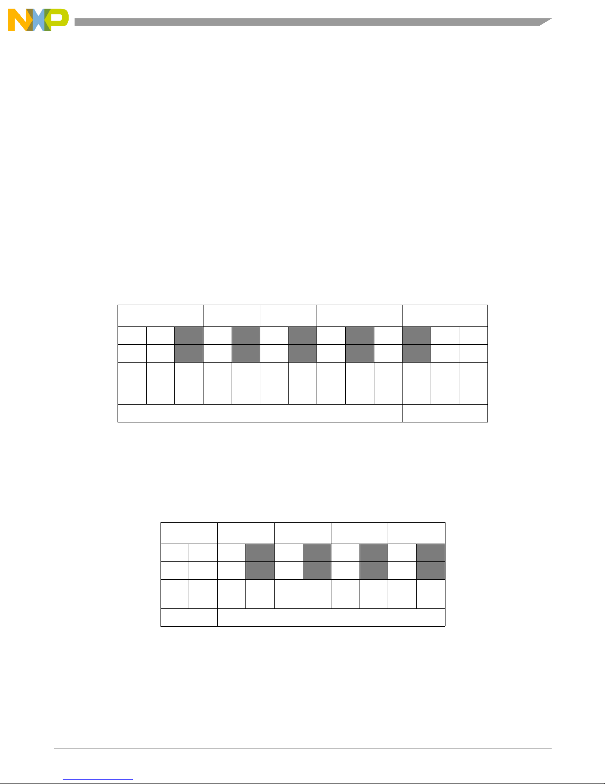
2.2.1 JP1/JP2 - S/PDIF Transmitter Output
The JP1 and JP2 headers are designed to allow selection of the S/PDIF output sources driven by the daughterboard (DSP), AKM 4101 S/PDIF
transmitter, or AKM 4114 S/PDIF receiver. The DSP option on the se jumpers is for future flexibility to allo w for m ultiple S/PDIF signals t o
be sourced from the daughterboard directly. One of the S/PDIF signals (TXSD4, TXSD5, o r TXSD6) can be directed to the TX4 output by
selecting it, using JP 2 and selecting the 4101TX4 option in the TX4 section of JP1. The 4114TX jumper option on TX4 is to allow direct
connection of the S/PDIF receiver relay to S/PDIF out. The ADO jumper option on TX1 allows the S/PDIF transmitter (DAX port) of certain
DSPs to be connected to the S/PDIF output connector.
2.2.2 JP3/JP4 – S/PDIF Receiver Input
The JP3 jumper allows for har dware configuration of the AKM 4114 S/PDIF receiver. The default setting is for software control mode and
the AKM 4114 is configured by the Motorola HC908GP32 configuration microcontroller on the motherboard.
The JP4 jumper controls the S/PDIF receiver input source to allow direct routing to the daughterboard using the DSP setting or selecting
connection to the AKM 4114 (default).
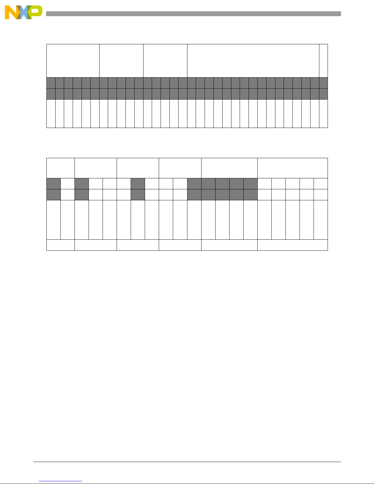
2.2.3 JP5 — Pass-thru Header
This jumper block is included to give convenient access to all the critical audio clocks and data lines. These jumpers can be removed to allow
for rerouting of the audio sign als withi n the board an d to allow fo r expansion to external boards. As an example, this header could be used to
connect to an external audio codec board for evaluation of the Motorol a DSP with a specific audio codec.
Table 2-1. JP1 / JP2 – S/PDIF Transmitter Output
TX1 TX2 TX3 TX4 4101TX4
* * * * * * * * * * * * *
* * * * * * * * * * * * *
ADO
DSP
4101
DSP
4101
DSP
4101
DSP
4101TX4
4114TX
TXSD4
TXSD5
TXSD6
JP1 JP2
Table 2-2. JP3 / JP4 – S/PDIF Receiver Input
IN=HI RX1 RX2 RX3 RX4
* * * * * * * * * *
* * * * * * * * * *
DIF2
DIF0
DSP
4114
DSP
4114
DSP
4114
DSP
4114
JP3 JP4
Page 10
DSPAUDIOEVM Users Guide, Rev. 2.4
This document contains information on a new product. Specifications and information herein are subject ot change without notice.
4 Freescale Semiconductor
Configuration Jumpers
2.2.4 Debugger and Microcontroller Configuration
2.2.4.1 PJ6 Debug MPU Crystal Selection
The JP6 jumper is for selection of RS232 or USB co mmunication when using the SDI debugger. Note that USB mode is not possible when
using the Win NT software version. The RS 23 2 positi on sho uld b e jumpered when the RS232 interface is used for the SDI debugger, and the
USB/PGM position should be used when using the USB interface for the SDI debugger or when reprogramming of the Debug Micro is
required. Only one of these jumpers should be connected at any one time. Use of the wrong jumper setting will cause SDI communication
failure to occur or a reduction in the data transfer rate.
2.2.4.2 JP7 – MPU Program Control
The JP7 jumpers are only used when the on-b oard microcontrollers are to be re-programmed . P l acing a jumper in the PGM position places
the selected microcontroller in program mode upon power-on. The microcontroller to be programmed is selected by placing a jumper in either
the DEBUG MPU or CONFIG MPU positions. With no jumper in the PGM position, the other two jumpers are ignored.
2.2.4.3 JP8 – SHI Debug Source Selection
The JP8 jumpers are for selection of various debugger modes. The default selection is for SDI debugge r use. The PPI port can be used with
legacy "PPP Development Interface" software and a PPI cable although the latest SDI debugger software is the preferred option for future
upgradability and support. The third option, CONFIG MPU, is not currentl y supported on the EVM. Only one jumper position sho uld be used
at any one time.
2.2.4.4 JP9 – OnCE/JTAG Debugger Source Selection
The JP9 jumpers are used for selection of alternative debugging tools such as the Suite 56 OnCE interface mentioned earlier. To use this,
simply connect to a host PC with a paralle l cable and have a jumper in the PARALLEL positions. The OnCE jumper option can be used if the
user wishes to connect an external OnCE/JTAG debugger interface to the board. The USB/RS232 option is not currently supported and only
one jumper should be inserted at a time.
Table 2-3. JP5 — PASS-THRU Header
MCLK BICK LRCLK SERIAL I / O
M
U
T
E
* * * * * * * * * * * * * * * * * * * * * * * * * * * * * * * *
* * * * * * * * * * * * * * * * * * * * * * * * * * * * * * * *
RX01
RX02
TX
ADC
DACA
DACB
RXTXADC
DACA
DACB
RXTXADC
DACA
DACB
RX
ADC1
ADC2
TXS01
DACA1/2
TXS02
DACA3/4
TXSD3
DACA5/6
TXSD4
DACB 1/2
TXSD5
DACB3/4
TXCD6
DACB5/6
MUTE
Table 2-4. Debug and Crystal MPU Settings
JB16
EXTAL
PGM MD SHI JTAG MPU COM AUX IN=HI
* * * * * * * * * * * * * * * * * * * *
* * * * * * * * * * * * * * * * * * * *
RS232
USB/PGM
DEBUG MPU
CONFIG MPU
PGM
PPI PORT
DEBUG MPU
CONFIG MPU
OnCE
USB/RS232
PARALLEL
COM0
COM1
COM2
COM3
AUX1
AUX2
AUX3
AUX4
AUX5
JP6 JP7 JP8 JP9 JP10 JP11
Page 11
Signal Headers
DSPAUDIOEVM Users Guide, Rev. 2.4
This document contains information on a new product. Specifications and information herein are subject ot change without notice.
Freescale Semiconductor 5
2.2.4.5 JP10 – Config / Debug MPU Communication
The JP10 jumpers provide a communication port between the debug microcontroller and the configuration microcontroller. When the SDI
debugger is used and the AUX5 jumper is out, the SDI debugger interface controls the audio input source. The JP10 jumpers pro vi de a
communication port be tween the debug m icrocontroller and the configuration microcontroller. When the SDI debugger is used, and the AUX5
jumper is out, the SDI debugger interface controls the audio input source. To allow this, all JP10 jumpers should be populated.
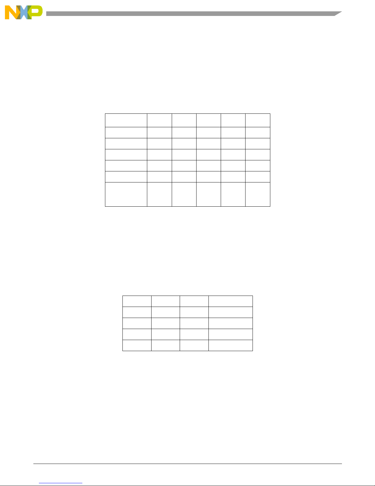
2.2.4.6 JP11 – AUX Mode Input Source Selection
The JP11 jumpers are present as an alternative to using the SDI debugger software to select between the various inputs available. If the AUX5
jumper is present then the following jumper setting s will result in the input selectio n sho w n in Table 2-5
2.3 Signal Headers
These headers allow for external debu gger connections, analog output signal measurement, and GPIO access.
2.3.1 P1 — PPI Header
The PPI header connections are to allow for backwards compatibility with existing PPI software tool set and to allow easy access to the SHI
port connections f r om the motherboard. Note that when using PPI source, JP8 must have PPI Port jumper in place.
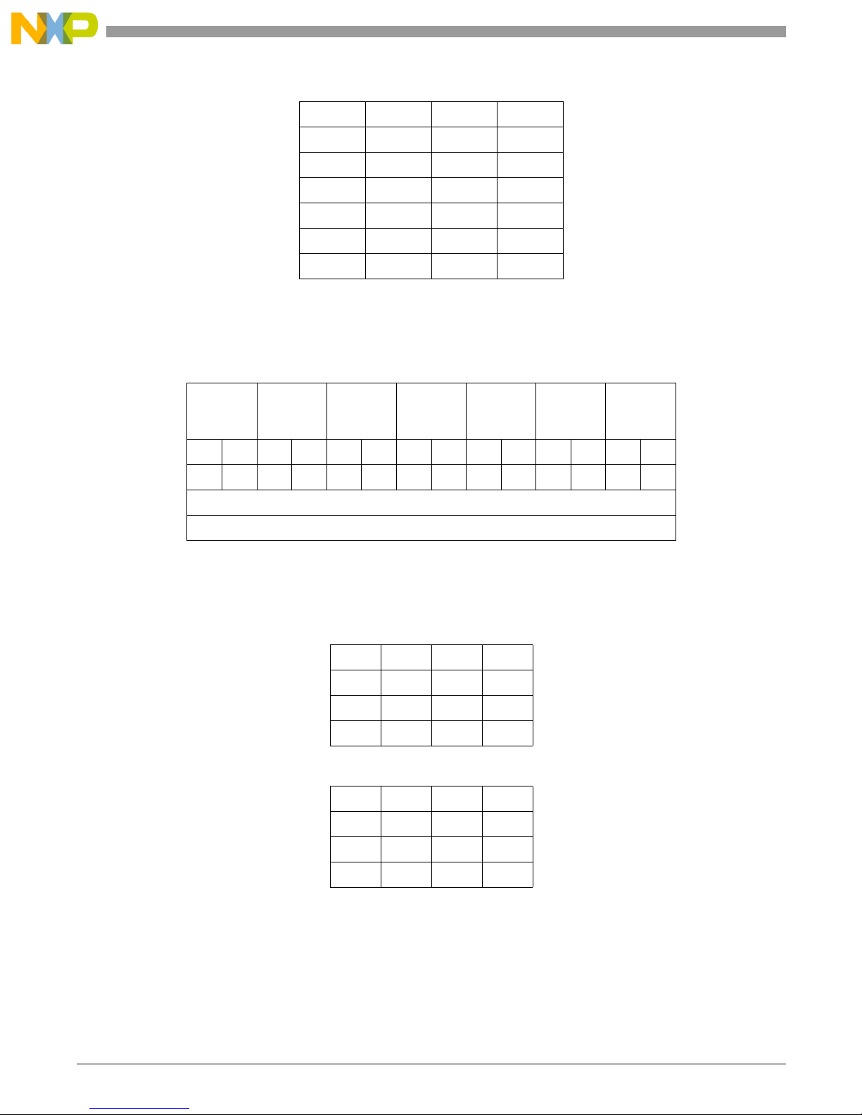
2.3.2 P2 — OnCE Header
The P2 OnCE header is for connection of an external OnCE/JTAG debugger tool to the OnCE/JTAG port of the DSP on the daughterboard.
Further explanation of the OnCE /JTAG signal definition can be found in the DSP u sers guid e s. The P2 OnCE header is for connection of an
external OnCE/JTAG debugger tool to the OnCE/JTAG port of the DSP on the daughterboard. Further explanation of the OnCE/JTAG signal
definition can be found in the DSP users guides. Note that when using an external OnCE/JTAG debugger tool, the JP9 JTAG jumper should
be in the "OnCE" position.
Table 2-5. JP11 Selections
Input Selected Aux5 Aux4* Aux3 Aux2 Aux1
RX1 1 0 0 0 0
RX2 1 0 0 0 1
RX3 1 0 0 1 0
RX4 1 0 0 1 1
AIN1 1 0 1 0 0
SDI
debugger
selects input
0 X X X X
* When the Aux5 jumper is present, the Aux4 jumper directly
controls the mute functionality of the EVM motherboard.
Table 2-6. P1 — PPI Header
NC(1) * * SS/HA2
GND * * SCK/SCL
GND * * HREQ
SDA * * MOSI / HA0
VDD * * MISO
Page 12
DSPAUDIOEVM Users Guide, Rev. 2.4
This document contains information on a new product. Specifications and information herein are subject ot change without notice.
6 Freescale Semiconductor
On-board Debugger Connections
2.3.3 P3 — ANALOG I/O
The Analog I/O header allows for analog acc ess to input signals before the A/D (AIN1) op-amp stage and th e output signals after the D/A
(AO1-6) op-amp stage. This section is provided for ease of analog measurement and anal og I/O connector relocation.
2.3.4 TP1 / TP2 Headers
TP1 and TP2 jumper blocks route to daughterboard for GPIO test points and future flexibility. On the DSP 56362/6/7 parts, as an example,
these headers are connected to the DSP HDI08 port. See daughterboard schematics and ap pendix for device specifics.
2.4 On-board Debugger Connections
The connectors discussed in this section are the on-board debuggers. For specific information on using the debuggers, see the relevant User’s
Manuals.
2.4.1 J2 — USB Interface
This connector is used in conjunction with the SDI software to debug a DSP using USB communications. See Section 2.2.4, Debugger and
Microcontroller Configuration for the proper jumper settings to use this interface.
Table 2-7. P2 — OnCE Header
TDI(1) * * GND
TDO * * GND
TCK * * GND
N/C * KEY
RESET * * TMS
VDD * * N/C
N/C * * N/C
Table 2-8. P3 — Analog I / O
AO6 AO5 AO4 AO 3 AO2 AO1 AIN1
R L R L R L R L R L R L R L
* * * * * * * * * * * * * *
* * * * * * * * * * * * * *
GND
P3
Table 2-9. TP1 Header — GP TP1–8
TP1 * * TP8
TP2 * * TP7
TP3 * * TP6
TP4 * * TP5
Table 2-10. TP2 Header — GP TP9–16
TP9 * * TP16
TP10 * * TP15
TP11 * * TP14
TP12 * * TP13
Page 13
External I/O
DSPAUDIOEVM Users Guide, Rev. 2.4
This document contains information on a new product. Specifications and information herein are subject ot change without notice.
Freescale Semiconductor 7
2.4.2 J3 — RS232 Interface
This connector can be used for debu gging or for in-fie ld updating of th e microcontrolle r code. T o use th is port for debugg ing, the SDI software
must be used. See Section 2.2.4, Debugger and Microcontroller Configuration for the proper jumper settings to use this interface.
2.4.3 J4 — Parallel Port Debugger Interface
This connector is used for the on-board Suite56 Parallel Port Command Converter. In conjunction with the Suite56 software, this interface
provides a high- speed debugger connection through the JTAG/OnCE port of the DS P. See Section 2.2.4 , Debugger and Mi c rocontroller
Configuration for the proper jumper settings to use this interface.
2.5 External I/O
2.5.1 J9 / J10 — Microphone Inputs
There are two microp hone inputs availabl e at 1/8inch microphone connectors J9 and J10 labeled MIC1 and MIC2. Th ese can also be
monitored via hea dphones by switching MIC1 and MIC2 on. The input levels of these c an be adjusted with the potentiometers at RV1 and
RV2 labeled MIC1 LEVEL and MIC2 LEVEL. These signals are connected to th e ADC2 A/D converter.
NOTE
If 1/4 inch to 1/8 inch adaptors are used for the mi crophone connection use only stereo-st ereo or
mono-mono style adapters. Stereo-mono o r mono-stereo adapters will result in a short of the
incoming audio signal to ground.
2.5.1.1 RV1/RV2 - Microphone Gain Control
These potentiometer s control the input levels for MIC1 an d MIC2 respectively. To prevent damage, alway s sta rt with th e se co ntrols in a low
setting, i.e., twisted left. These inputs can be monitored directly, using the on-board headphone amplifier.
2.5.2 J11 / J12 — Analog Outputs
Fixed pre-amp outputs (Variable through Digital Volume control on the DSP) are provided for 12 channels of output. These RCA connections
can be fed into a variable or fixed amplifier stage. Care should be taken to verify signal integrity before connecting to large fixed amplifiers
to avoid audible noise or sp eaker damage.
These outputs are located at J11 and J12.
If using the Software Architecture, the analog outputs correspond to the following:
AOUT1 WHITE Left Main
AOUT1 RED Right Main
AOUT2 WHITE Left Surround
AOUT2 RED Right Surround
AOUT3 WHITE Center
AOUT3 RED Subwoofer
AOUT4 WHITE Left Back
AOUT4 RED Right Back
Table 2-11. J11
AOUT1 AOUT2 AOUT3
White White White
Red Red Red
Table 2-12. J12
AOUT4 AOUT5 AOUT6
White White White
Red Red Red
Page 14
DSPAUDIOEVM Users Guide, Rev. 2.4
This document contains information on a new product. Specifications and information herein are subject ot change without notice.
8 Freescale Semiconductor
DSPX36XDB1
AOUT5 WHITE Left Secondary
AOUT5 RED Right Secondary
AOUT6 WHITE Unassigned
AOUT6 RED Unassigned
2.5.3 J13 — Headphone Outputs
These channels can also be monitored with the on-board headphone amplifier. The channel listened to is selected via switches SW2 and SW3.
Moving the switch to the right will enable the corresponding channel. There are right and left volume sliders (RV3 and RV4) to allow
variations in volume level and balance control. Headphones should be plugged in to the J13 1/8-inch headphone connector.
2.5.3.1 SW2 / SW3 — Channel Select
These switches control what is routed to the on-board headphone amplifier. Moving the switch to the right will enable the corresponding
channel. Multiple switches/channels can be enabled at one time, and the signals will be summed into the corresponding headphone channel.
2.5.3.2 RV3 / RV4 — Headphone Volume Select
These sliders allow for volume and balance adjustment for the headphone amplifier. T o help prevent damage to headphones or hearing, always
start with the sliders in a low-volume position.
Chapter 3
DSP5636x DAUGHTERBOARD
3.1 DSPX36XDB1
This daughterboard supports the 56362, 56364, 56366, and 56367. The following sections describe the jumper and switch settings available
on the DSPX36XDB1. A schematic for this daughterboard can be found in Appendix A.
3.2 Mode Selection
Var ious boot-up modes can be selected via the MO DE pins and pins PB13 and PB 14 settings can be deter m ined using switch bank SW1.
Switch position “ON” = sign al hi gh. Table 3-1 shows the modes available for the 56362/366/367. Table 3-2 shows the modes available for the
56364. See device-specific user manual for full details of each boot mode.
NOTE
All other modes are reser ved and should not be used.
Table 3-1. Mode Selection for 56362/366/367
MODD MODC MODB MODA PB14* PB13* Mode
0 0 0 0 X X Expanded mode (execute from $C00000)
0 0 0 1 X X Bootstrap from external FLASH
0 0 1 0 0 1 Bootstrap SA in SPI mode*
0 0 1 0 1 1 Bootstrap SA in I2C mode*
0 1 0 1 X X Boot from SHI (slave SPI mode)
0 1 1 1 X X Boot from SHI (slave I2C mode)
1 0 0 0 X X Expanded mode (execute from $008000)
1 1 0 0 X X Bootstrap in HDI08 ISA mode
1 1 0 1 X X Bootstrap in HDI08 HC11 mode
1 1 1 0 X X Bootstrap in HDI08 8051 mode
1 1 1 1 X X Bootstrap in HDI08 69302 mode
* These modes are only applicable to DSPs which have the embedded ROM based Software Architecture (SA).
Page 15
Memory
DSPAUDIOEVM Users Guide, Rev. 2.4
This document contains information on a new product. Specifications and information herein are subject ot change without notice.
Freescale Semiconductor 9
3.3 Memory
The daughter board i nclu des thr ee 12 8Kx8 S RAM (o ne 128 Kx8 S RAM fo r the 56 364 daught erbo ard). T here is also a 512K x8 FLA SH de vice
resident on the board. From factory the FLASH is programmed with an audio passthru code to allow simple verification of initial board
operations. See Section 1.8, Running the Passthru Code for an explanation of running the passthru code.
3.4 JP11 - Clock Selection
Jumper bank JP11 allows for the following clocking modes:
OSC – Clock DSP from canned oscillator at U7 (not Populated)
XTAL – Clock DSP from 24.576MHz crystal at X1 (default mode)
EXT – Clock DSP fro m motherboard 24 .576MHz clock source
Only one of the JP11 options sho uld be popu la ted at the same time .
3.5 Daughterboard Audio I / O and Clock Control Header
3.5.1 TIO0 – Timmer Port
This is connected directly to the TIO0 pin on the DSP.
3.5.2 JP1 - Synchronous/Asynchronous Clock Control
This jumper set controls whether or not the DSP is in synchronous or asynchronous mode. Position B allows the DSP GPIO (pin PB9) to
choose the mode. Position C forces the mode to be asynchronous, and no jumper forces synchronous mode. In synchronous mode FST is
connected to FSR, and SCKT is connected to SCKR on the ESAI port of the DSP.
Table 3-2. Mode Selection for 56364
MODD MODC MODB MODA Mode
0 X 0 0 Jump to PROM starting address
0 X 0 1 Bootstrap from byte-wide memory
0 X 1 0 Reserved
0 X 1 1 Reserved for Burn-in testing
1 X 0 0 Reserved
1 X 0 1 Bootstrap from SHI (slave SPI mode)
1 X 1 0 Bootstrap from SHI (slave I2C mode, clock freeze enabled)
1 X 1 1 Bootstrap from SHI (slave I2C mode, clock freeze disabled
Table 3-3. Daughterboard Audio I / O and Clock Control Header
TIO0
Sync/Async
Sng/Dbl
FST_1
SCKT_1
FSR_1
SCKR_1
DSP MUTE
INTO
SDO5/SDI0
SDO4/SDI1
* * * * * * * * * * * * * * * * *
* * * * * * * * * * * * * * * * *
A B C D E F G H I J K L M N O P Q
TI0 JP1 JP2 JP3 JP4 JP5 JP6 JP7 JP8 JP9 JP10
Page 16

DSPAUDIOEVM Users Guide, Rev. 2.4
This document contains information on a new product. Specifications and information herein are subject ot change without notice.
10 Freescale Semiconductor
Daughterboard Audio I / O and Clock Control Header
3.5.3 JP2 – Single/Double Speed Clocking Control
This jumper set controls whether or not the motherboard is in single or double speed mode. Position D forces the motherboard into double
speed mode. Position E allows the DSP GPIO pin PB11 to control the mode (e.g., through a PPP), and no jumper forces single speed mode.
An example of this signal’s use is for decoding of DTS 96/24 content. In this mode, it is required to update the masterclock ration expectation
in the D/A converters and S/PDIF transmitters becau se the DTS 96/24 decode r doubles the au dio sample rate a s part of the de coding process.
3.5.4 JP3 - FST_1 Connection
This set of jumpers determines whic h fra me syn c cl oc k sour ce is u s ed fo r th e AKM DAC4_ 6 . Th e F p osition directs the ESAI_0 FST signal
to DAC4_6. Position G directs the ESAI_1 FST sign al to DAC4_6, and po pulation o f both jumpe rs will synchroniz e/short the two ES AI port
FST lines.
NOTE
Position F should always be populated when using a 56362 or 56364 daughterboard.
3.5.5 JP4 – SCKT_1 Connection
This set of jumpers determines which serial clock source is used for the AKM DAC4_6. Position H directs the ESAI_0 SCKT signal to
DAC4_6, position I directs the ESAI_1 SCKT signal to DAC4_6 and population of both jumpers will synchronize/short the two ESAI port
SCKT lines.
NOTE
Position H should alw a ys be populated when using a 56362 or 56364 daughter board.
3.5.6 JP5 - FSR_1 Connection
This jumper connects/shorts the FSR and FSR_1 signals together. No jumper means that the FSR_1 signal stops at the header.
3.5.7 JP6 - SCKR_1 Connection
This jumper connects/shorts the SCKR and SCKR_1 signals together. No jumper means that the SCKR_1 signal stops at the header.
3.5.8 JP7 - DSP MUTE Control
This jumper controls the mute signal whe n used in conjun ction with the Software Architecture or GPIO control . W ith the jump er in pla ce, the
mute control is connected to the DSP GPIO pin PB12. No jumper means that mu te functi on al ity will on ly be controlled by the motherboard.
3.5.9 JP8 - INT_0/SPDIF Error Flag Connection
This jumper connects the error flag signal from the AKM 4114 to the DSP GPIO pin PB15. This allo ws the DSP to b e in fo rmed o f the status
of the AKM 4114 S/PDIF receiver. If the connection is not desired this jumper can be removed.
3.5.10 JP9 - SDO5/SDI0 Configuration
This jumper set controls the signal con nections of SDO5/SDI0. Depending on the ESAI setting in the DSP, this pin can be conf igured as an
input or an output. A jumper in position N feeds the SDI0 signal from the ADC2 microphone source. A jumper in the O position feeds the
SDO5 signal to DAC4_6.
3.5.11 JP10 SDO4/SDI1 Configuration
This jumper set controls the input sou rce for SDI1. A jum per in the P position feeds the SDI1 signal from the AKM 41 1 4 S/PDIF receiver . A
jumper in the Q position feeds the SDI1 signal from ADC1. There is no available jumper set ting for use of the SDO4 signal.
Page 17
DSPX37XDB1
DSPAUDIOEVM Users Guide, Rev. 2.4
This document contains information on a new product. Specifications and information herein are subject ot change without notice.
Freescale Semiconductor 11
Chapter 4
DSP56371 DAUGHTERBOARD
4.1 DSPX37XDB1
The following s e c tio n d esc r ibes the jumper an d s w itch options for th e D S PX 37 X D B1. The schematic f or the daughterbo ard c an be found in
Section A, Schematics for clarification of all DSP connections.
NOTE
Two versions of the DSPX37XDB1 exist: Rev C and Rev D. You can determine the re vision by
looking at the bottom side of the board just below the serial num ber. This section documents Rev D
of the board which is the cu rrent pr oduction revision. Wh ile the j umper sets are numb ered dif ferently
between the revisions, the functional descriptions remain the same. The only functional difference
between revisions is the additio n of the boot from on-board serial EEPROM av ailable only on the R ev
D board. Schematics for the Rev C board are not included in this manual but are available upon
request.
NOTE
All other modes are reser ved and should not be used.
4.2 Mode Selection
Various boot-up modes can be selected via the MODE pins and pins TP13 and TP14 settings can be determined using switch bank SW1.
Switch position “ON”= signal high. See the DSP56371 user manual for full details.
4.3 Memory
The DSPX37XDB1 daughterboard includes one 1Mx8 EEPROM accessed by an I2C-compatible bus. This memory comes pre-programmed
with a basic audio passthru code to allow simple verification of the initial board operations. See Section 1.8, Running the Passthru Code for
more details.
4.4 JP1 - Clock Selection
Jumper bank JP1 allows for the following clocking modes:
OSC – Clock DSP from canned oscillator at U7 (not Populated)
XTAL – Clock DSP from 24.576MHz crystal at X1 (default mode)
EXT – Clock DSP fro m motherboard 24 .576MHz clock source
Only one of the JP1 options should be populated at the same time.
Table 4-1. Mode Selection
MODD MODC MODB MODA TP14 TP13 Mode
0 0 1 0 0 1 Bootstrap SA in SPI mode
0 0 1 0 1 1 Bootstrap SA in I2C mode
0 1 0 1 X X Bootstrap from SHI (slave SPI) mode
0 1 1 1 X X Bootstrap from SHI (slave I2C) mode
1 0 0 1 X X Bootstrap from SHI (serial EEPROM) mode
Page 18
DSPAUDIOEVM Users Guide, Rev. 2.4
This document contains information on a new product. Specifications and information herein are subject ot change without notice.
12 Freescale Semiconductor
Daughterboard Audio I / O and Clock Control Header
4.5 Daughterboard Audio I / O and Clock Control Header
4.5.1 JP3 - Synchronous/Asynchronous Clock Control
This jumper set controls whether or not the DSP is in synchronous or asynchronous mode. Position A allows the DSP GPIO (pin PB1) to
choose the mode. Position B forces the mode to be asynchronous, and no jumper forces synchronous mode. In synchronous mode FST is
connected to FSR, and SCKT is connected to SCKR on the ESAI port of the DSP.
4.5.2 JP4 – Single/Double Speed Clocking Control
This jumper set controls whether or not the motherboard is in single or double speed mode. Position C forces the motherboard into double
speed mode. Position D allows the DSP GPIO pin PE10 to control the mode (e.g., through a PPP), and no jumper forces single speed mode.
An example of this signal’s use is for decoding of DTS 96/24 content. In this mode, it is required to update the masterclock ration expectation
in the D/A converters and S/PDIF transmitters becau se the DTS 96/24 decode r doubles the au dio sample rate a s part of the de coding process.
4.5.3 JP5 - DSP MUTE Control
This jumper controls the mute signal whe n used in conjun ction with the Software Architecture or GPIO control . W ith the jump er in pla ce, the
mute control is connected to th e DSP GPIO pi n PE11. No jumper means tha t mute fun c tio nality will o nl y be c ontro lle d b y the motherboard.
4.5.4 JP6 - FSR_1 Connection
This jumper connects/shorts t he FSR and FSR_1 signals together. No jumper means that the FSR_1 signal stops at header P1.
4.5.5 JP7 - SCKR_1 Connection
This jumper connects/shorts the SCKR and SCKR_1 signals together. No jumper means that the SCKR_1 signal st ops at header P1.
4.5.6 JP8 - SCKT_1 Connection
This set of jumpers determines which serial clock source is used for the AKM DAC4_6. Position I directs the ESAI_0 SCKT signal to
DAC4_6, position H directs the ESAI_1 SCKT signal to DAC4_6 and population of both jumpers will syn chr o nize /shor t th e two ESAI port
SCKT lines.
4.5.7 JP9 - FST_1 Connection
This set of jumpers determines which frame sync clock source is use d for the AKM DAC4_6. The K position di rects the ESAI FST sign al to
DAC4_6. Position J directs the ESAI_1 FST signal to DAC4_6, and populati on of both jumpers will synchronize/short the two ESAI port
FST lines.
4.5.8 JP10 - SDO5/SDI0 Configuration
This jumper set controls the signal con nections of SDO5/SDI0. Depending on the ESAI setting in the DSP, this pin can be conf igured as an
input or an output. A jumper in position L feeds the SDI0 signal from the ADC2 microphone source. A jumper in the M position feeds the
SDO5 signal to DAC4_6.
Table 4-2. Daughterboard Audio I/O and clock Control Header
SYNC/ASYNC
SNG/DBL
DSP MUTE
FSR_1
SCKR_1
SCKT_1
FST_1
SD05/SD10
SD04/SD11
4114MCLK
PF8MCLK
JCLT_1
LED = DSP PF6
LED = 4114 INT0
4114 INT0 = DSP PF6
* * * * * * * * * * * * * * * * * * * * *
* * * * * * * * * * * * * * * * * * * * *
A B C D E F G H I J K L M N O P Q R S T U
JP3 JP4 JP5 JP6 JP7 JP8 JP9 JP10 JP11 JP12 JP13 JP14
Page 19

JP2 - I2C Boot ROM Enable
DSPAUDIOEVM Users Guide, Rev. 2.4
This document contains information on a new product. Specifications and information herein are subject ot change without notice.
Freescale Semiconductor 13
4.5.9 JP11 - SDO4/SDI1 Configuration
This jumper set controls the input source for SDI1. A jumper in the N po sition feeds the SDI1 signal fro m the AKM 41 1 4 S/P DIF receiver . A
jumper in the O position feeds the SDI1 signal from ADC1. There is no available jumper set ting for use of the SDO4 signal.
4.5.10 JP12 - Master Clock Configuration Control
This set of jumpers allows for numerous routing options of the master clock. A jumper in the P position feeds the master clock from the
AKM4114 SPDIF receiver to the ESAI HCKT , HCKR and ACI pins as well as the AKM4114 SPDIF transmitter, ADC, DAC1-3 and DAC4-6.
A jumper in the R position connects/shorts the HCKT_1 signal to the HCKT, HCKR and ACI signals. Jumper positions P and R may be used
together to feed the AKM4114 SPDIF master clock to the HCKT_1 input. Jumper position Q is reserved for future expansion.
4.5.11 JP13 - SPDIF Lock LED Source Select
This jumper set controls the source for the SPDIF lock LED, D6, on the motherboard. A jumper in location T allows connects LED, D6, to
the AKM4114 lock signal output. Jumper position S is reserved fo r future expansion.
4.5.12 JP14 - SPDIF Lock Connection
This jumper connects the AKM4114 lock signal to GPIO signal PF6 if jumper set JP13 has a jumper in location T.
4.6 JP2 - I2C Boot ROM Enable
This set of jumpers allows the on-board serial EEPROM to be remove d from th e SHI bus. Jump er location V conn ects the serial data line to
the DSP MISO signal and location W co nnects the serial clock line to the DSP SCK signal. Both jumpers must be placed t o use bootstrap
mode 9.
4.7 P1 - ESAI Receive In
This header allows for external connections to ESAI and ESAI_1 receiver signals and GPIO. The odd row is ground while the even row of
pins is signal. This provides ground isolation between each signal when used with ribbon cable connecto rs.
4.8 P2 - ESAI Transmit Out
This header allows for external connections to ESAI and ESAI_1 transmitter signals and GPIO. The odd row is ground while the even row of
pins is signal. This provides ground isolation between each signal when used with ribbon cable connecto rs.
Page 20

DSPAUDIOEVM Users Guide, Rev. 2.4
This document contains information on a new product. Specifications and information herein are subject ot change without notice.
14 Freescale Semiconductor
DSPX374DB1
Chapter 5
DSP56374 Daughterboard
5.1 DSPX374DB1
This daughterboar d supports all versions of the 56374. The following sections describe the jumper and switch options available on the
DSPX374DB1. The schematic for this daughterboard can be found in Appendix A.
5.2 Mode Selection
Var ious bootstrap modes can be selected via switch bank SW1. Table 5-1 shows the switch configuration for each available mode. See the
56374 User’s Manual for full details on each mode.
NOTE
All other modes are reser ved and should not be used.
5.3 Memory
The DSPX37XDB1 daughterboard includes one 1Mx8 EEPROM accessed by an I2C-compatible bus. This memory comes pre-programmed
with a basic audio passthru code to allow si mple verific atio n o f the init ia l board op er ati ons . Se e Section 1.8, Running the Passthru Code for
more details.
5.4 JP12 – Clock Selection
Jumper bank JP12 allows for the following clocking modes:
XTAL – Clock DSP from 24.576MHz crystal at X1 using the DSP’s internal oscillator
EXT – Clock DSP from motherboard 24.576MHz clock source
OSC – Clock DSP from canned oscillator at U4 (not populated)
When using the XTAL clocking mode both XTAL jumpers must be placed ( this is th e defau lt mode of op eration ). When using ot her clocking
modes, both XTAL jumpers must be removed. Only one clocking mode should b e used at the same time
Table 5-1. Mode Selection
MODD MODC MODB MODA Mode
0 0 1 0 Bootstrap SA in SPI mode
0 1 0 1 Bootstrap from SHI (slave SPI) mode
0 1 1 0 Bootstrap from SHI (slave I2C, HCKFR=1) mode
0 1 1 1 Bootstrap from SHI (slave I2C, HCKFR=0) mode
1 0 0 1 Bootstrap from SHI (serial EEPROM, HCKFR=1) mode
1 0 1 1 Bootstrap from SHI (serial EEPROM) mode
1 1 0 0 Bootstrap from SHI (serial SPI EEPROM) mode
1 1 1 0 Bootstrap SA (default HLX) in SPI mode
1 1 1 0 Bootstrap SA in I2C (HCKFR=0) mode
1 1 1 1 Bootstrap SA in I2C (HCKFR=1) mode
Page 21

Daughterboard Audio I/O and Clock Control Header
DSPAUDIOEVM Users Guide, Rev. 2.4
This document contains information on a new product. Specifications and information herein are subject ot change without notice.
Freescale Semiconductor 15
5.5 Daughterboard Audio I/O and Clock Control Header
5.5.1 JP1 – Synchronous/Asynchronous Clock Control
This jumper set controls whether or not the DSP is in synchronous or asynchronous mode. Position A allows the DSP GPIO (pin PG7) to
choose the mode. Position B forces the mode t o be asynchronous and no jumper forces synchronous mode. In synchronous mode FST is
connected to FSR and SC KT is connected to SCKR on the ES AI port of the DSP.
5.5.2 JP2 – Single/Double Speed Clocking Control
This jumper pair controls whether or not the motherboard is in single or double speed mode. Positio n C forces the moth er bo ar d i nto double
speed mode. Position D allows the DSP GPI O (pin PG6 ) to c ontrol th e mo de a nd n o jum per fo rces sin gle spe ed m ode. Th is ju mpe r is useful
when implementing a DTS 96/24 decoder.
5.5.3 JP3 – FSR_1 Connection
This jumper connects/shorts t he FSR and FSR_1 signals together. No jumper means that the FSR_1 signal stops at header P1.
5.5.4 JP4 – SCKR_1 Connection
This jumper connects/shorts the SCKR and SCKR_1 signals together. No jumper means that the SCKR_1 signal st ops at header P1.
5.5.5 JP5 – SDO5/SDI0 Configuration
This jumper pair controls the input source for SDI0. A jumper in position G feeds the SDI0 signal from the AKM 4114 S/PDIF receiver. A
jumper in position H feeds the SDI0 signal from ADC1. There is no available jumper setting for use of the SDO5 signal.
5.5.6 JP6 – SDO4/SDI1 Configuration
This jumper set controls the signal c onnections of SDO4/S DI1. Depending on the ES AI configuration in th e DSP , this signal can be c onfigu red
as an output (SDO4) or an input (SDI1). A jumper in position I feeds the SDI1 signal from ADC1. A jumper in position J feeds the SDO4
signal to DAC4-6.
5.5.7 JP7 – Watchdog Timer Connection
This jumper connects the on-chip watchdog timer output to the DSP reset circuit. By placing a jumper in position K the on-chip watchdog
timer can generate a hardware reset to the DSP. If no jumper is placed the watchdog timer is removed from the reset circuit.
5.5.8 JP8 – SD03/SDI2 Configuration
This jumper pair controls the signal connections of SDO3/SDI2. Depending on the ESAI configuration in the DSP, this signal can be
configured as an output (SDO3) or an input (SDI1). A jumper i n po sition L feeds the SDI1 signal f rom the ADC2 microphone sour ce. A
jumper in position M feeds the SDO3 signal to DAC 4-6.
Table 5-2. Daughterboard Audio I/O and clock Control Header
SYNC/ASYNC
SNG/DBL
FSR_1
SCKR_1
SD05/SD10
SD04/SD11
WDT/RESET
SD03/SD12
FST_1
FST
SCKT_1
SCKT
DSP MUTE
* * * * * * * * * * * * * * * * * *
* * * * * * * * * * * * * * * * * *
A B C D E F G H I J K L M N O P Q R
JP1 JP2 JP3 JP4 JP5 JP6 JP7 JP8 JP9 JP10 JP11
Page 22

DSPAUDIOEVM Users Guide, Rev. 2.4
This document contains information on a new product. Specifications and information herein are subject ot change without notice.
16 Freescale Semiconductor
Daughterboard Audio I/O and Clock Control Header
5.5.9 JP9 – FST/FST_1 Selection
This jumper set determines which frame sync clock source is used for DAC4-6. A jumper in position O directs the ESAI FST signal to
DAC4-6. A jumper in position N directs the ESAI_1 FST signal to DAC4-6. If both jumpers are placed this will connect/short the FST and
FST_1 signal s together .
5.5.10 JP10 – SCKT/SCKT_1 Selection
This jumper pair controls which serial clock source is used for DAC4-6. A jumper in position Q direct s the ESAI SCKT signal to DAC4-6.
A jumper in position P directs the ESAI_1 SCKT signal to DAC4-6. If both jumpers are placed this will connect/short the SCKT an d SCKT_1
signals together.
5.5.11 JP11 – DSP Mute Control
This jumper controls the mute signal when used in conjunction with the Software Architecture or GPIO control. W ith the jum per in place the
mute control is connected to the DSP GPIO (pinPG5). No jumper means that the mute functionality will only be controlled by the
motherboard.
5.5.12 JP13 – I2C Boot ROM Enable
This set of jumpers allows the on-board serial EEPROM to be removed from the SHI bus. Jumper location W connects the serial data line to
the DSP MISO signal and location X connects the serial clock line to the DSP SCK signal. Bot h j umpers must be placed to use bootstrap
modes 9 or B.
5.5.13 JP14 – S/PDIF Lock Control
This jumper is designed for future compatibility. For proper operation a jumper should be placed in position U.
5.5.14 JP15 – Master Clock Control
This jumper pair allows the DSP to supply a master tran smit clock from either ESAI port vi a the HCKT signal. A jumper in position S sources
the transmit master clock from the AKM 4114 S/PDIF receiver, while a jumper in pos iti on T sources the transmit master clock from either
HCKT or HCKT_1 (thes e signals are connected/shorted together in either jumper position).
5.5.15 P1 – ESAI Receive In
This header allows for external connections to ESAI and ESAI_1 receiver signals and GPIO. The odd row is ground while the even row of
pins is signal. This provides ground isolation between each signal when used with ribbon cable connecto rs.
5.5.16 P2 – ESAI Transmit Out
This header allows for external connections to ESAI and ESAI_1 transmitter signals and GPIO. The odd row is ground while the even row of
pins is signal. This provides ground isolation between each signal when used with ribbon cable connecto rs.
Page 23

Motherboard Schematics
DSPAUDIOEVM Users Guide, Rev. 2.4
This document contains information on a new product. Specifications and information herein are subject ot change without notice.
Freescale Semiconductor 17
Appendix A
Schematics
A.1 Motherboard Schematics
Figure A-1. Motherboard Block Diagram
MM
Page 24

DSPAUDIOEVM Users Guide, Rev. 2.4
This document contains information on a new product. Specifications and information herein are subject ot change without notice.
18 Freescale Semiconductor
Motherboard Schematics
Figure A-2. Motherboard DACA 1-3
MM
Page 25

Motherboard Schematics
DSPAUDIOEVM Users Guide, Rev. 2.4
This document contains information on a new product. Specifications and information herein are subject ot change without notice.
Freescale Semiconductor 19
Figure A-3. Motherboard DACB 4-6
MM
Page 26

DSPAUDIOEVM Users Guide, Rev. 2.4
This document contains information on a new product. Specifications and information herein are subject ot change without notice.
20 Freescale Semiconductor
Motherboard Schematics
Figure A-4. Motherboard ADC 1-2
MM
Page 27

Motherboard Schematics
DSPAUDIOEVM Users Guide, Rev. 2.4
This document contains information on a new product. Specifications and information herein are subject ot change without notice.
Freescale Semiconductor 21
Figure A-5. Motherboard Configuration MPU
MM
Page 28

DSPAUDIOEVM Users Guide, Rev. 2.4
This document contains information on a new product. Specifications and information herein are subject ot change without notice.
22 Freescale Semiconductor
Motherboard Schematics
Figure A-6. Motherboard Headphone Amplifier and Mixer
MM
Page 29

Motherboard Schematics
DSPAUDIOEVM Users Guide, Rev. 2.4
This document contains information on a new product. Specifications and information herein are subject ot change without notice.
Freescale Semiconductor 23
Figure A-7. Motherboard SPDIF
MM
Page 30

DSPAUDIOEVM Users Guide, Rev. 2.4
This document contains information on a new product. Specifications and information herein are subject ot change without notice.
24 Freescale Semiconductor
Motherboard Schematics
Figure A-8. Motherboard PPI and JTAG Command Converter
MM
Page 31
Motherboard Schematics
DSPAUDIOEVM Users Guide, Rev. 2.4
This document contains information on a new product. Specifications and information herein are subject ot change without notice.
Freescale Semiconductor 25
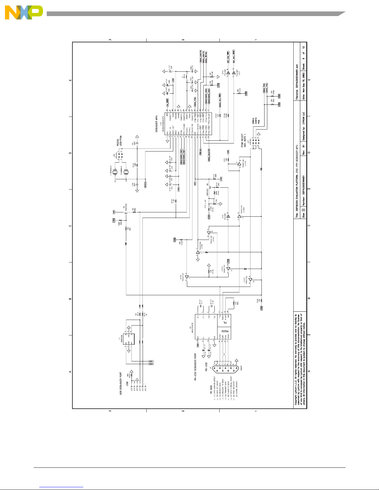
Figure A-9. Motherboard JTAG/PPI Debugger MPU
MM
Page 32

DSPAUDIOEVM Users Guide, Rev. 2.4
This document contains information on a new product. Specifications and information herein are subject ot change without notice.
26 Freescale Semiconductor
Motherboard Schematics
Figure A-10. Motherboard DSP Daughterboard Connectors
MM
Page 33

Motherboard Schematics
DSPAUDIOEVM Users Guide, Rev. 2.4
This document contains information on a new product. Specifications and information herein are subject ot change without notice.
Freescale Semiconductor 27
Figure A-11. Motherboard Power and MCLK Lost Detect and Systems Reset
MM
Page 34

DSPAUDIOEVM Users Guide, Rev. 2.4
This document contains information on a new product. Specifications and information herein are subject ot change without notice.
28 Freescale Semiconductor
Motherboard Schematics
Figure A-12. Motherboard Notes and Tables
MM
Page 35

DSP5636x Daughterboard Schematics
DSPAUDIOEVM Users Guide, Rev. 2.4
This document contains information on a new product. Specifications and information herein are subject ot change without notice.
Freescale Semiconductor 29
A.2 DSP5636x Daughterboard Schematics
Figure A-13. DSP5636x Daughterboard DSP Connections for DSP56362/366/367
MM
Page 36

DSPAUDIOEVM Users Guide, Rev. 2.4
This document contains information on a new product. Specifications and information herein are subject ot change without notice.
30 Freescale Semiconductor
DSP5636x Daughterboard Schematics
Figure A-14. DSP5636x Daughterboard DSP Connections for DSP56364
MM
Page 37

DSP5636x Daughterboard Schematics
DSPAUDIOEVM Users Guide, Rev. 2.4
This document contains information on a new product. Specifications and information herein are subject ot change without notice.
Freescale Semiconductor 31
Figure A-15. DSP5636x Daughterboard External Memory
MM
Page 38

DSPAUDIOEVM Users Guide, Rev. 2.4
This document contains information on a new product. Specifications and information herein are subject ot change without notice.
32 Freescale Semiconductor
DSP5636x Daughterboard Schematics
Figure A-16. DSP5636x Daughterboard Connectors
MM
Page 39

DSP56371 Daughterboard Schematics
DSPAUDIOEVM Users Guide, Rev. 2.4
This document contains information on a new product. Specifications and information herein are subject ot change without notice.
Freescale Semiconductor 33
A.3 DSP56371 Daughterboard Schematics
Figure A-17. DSP56371 Daughterboard DSP Connections
MM
Page 40

DSPAUDIOEVM Users Guide, Rev. 2.4
This document contains information on a new product. Specifications and information herein are subject ot change without notice.
34 Freescale Semiconductor
DSP56371 Daughterboard Schematics
Figure A-18. DSP56371 Daughterboard Connectors
MM
Page 41
DSP56374 Daughterboard Schematics
DSPAUDIOEVM Users Guide, Rev. 2.4
This document contains information on a new product. Specifications and information herein are subject ot change without notice.
Freescale Semiconductor 35
A.4 DSP56374 Daughterboard Schematics
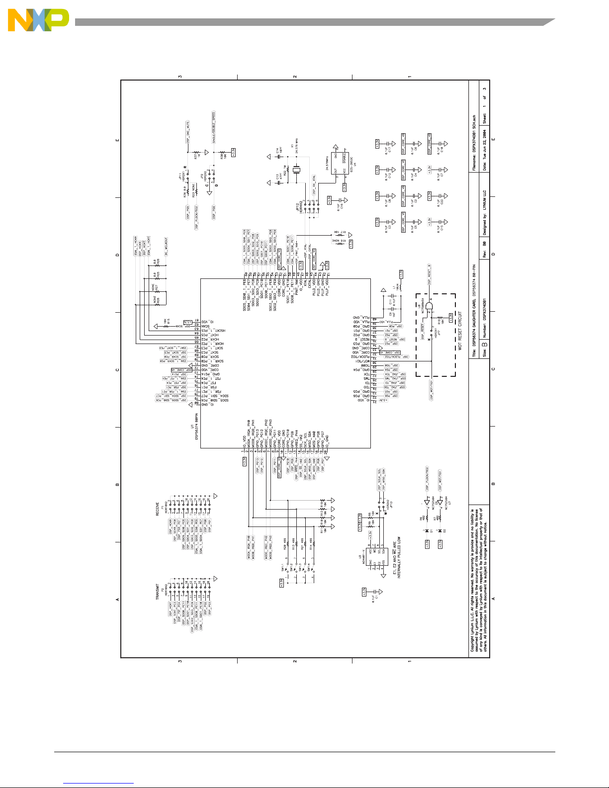
Figure A-19. DSP56374 Daughterboard 80-pin DSP Connections
SS
Page 42

DSPAUDIOEVM Users Guide, Rev. 2.4
This document contains information on a new product. Specifications and information herein are subject ot change without notice.
36 Freescale Semiconductor
DSP56374 Daughterboard Schematics
Figure A-20. DSP56374 Daughterboard 52-pin DSP Connections
SS
Page 43

DSP56374 Daughterboard Schematics
DSPAUDIOEVM Users Guide, Rev. 2.4
This document contains information on a new product. Specifications and information herein are subject ot change without notice.
Freescale Semiconductor 37
Figure A-21. DSP56374 Daughterboard Connectors
SS
Page 44

DSPAUDIOEVM Users Guide, Rev. 2.4
This document contains information on a new product. Specifications and information herein are subject ot change without notice.
38 Freescale Semiconductor
DSP56374 Daughterboard Schematics
Appendix B
EVM Bill of Materials
Table B-1. EVM Bill of Materials
RefDe
s
Val ue Part Number Description Manufacturer
C1 470UF EEV-FC1E471P Aluminum Electrolytic Capacitor/FC Series 470UF 25V Panasonic
C2 470UF EEV-FC1E471P Aluminum Electrolytic Capacitor/FC Series 470UF 25V Panasonic
C3 470UF EEV-FC1E471P Aluminum Electrolytic Capacitor/FC Series 470UF 25V Panasonic
C4 150PF C080COG101-151JNE 150 PF 5% COG 0805 100V Ceramic Chip Capacitor Venkel
C5 150PF C080COG101-151JNE 150 PF 5% COG 0805 100V Ceramic Chip Capacitor Venkel
C6 150PF C080COG101-151JNE 150 PF 5% COG 0805 100V Ceramic Chip Capacitor Venkel
C7 150PF C080COG101-151JNE 150 PF 5% COG 0805 100V Ceramic Chip Capacitor Venkel
C8 150PF C080COG101-151JNE 150 PF 5% COG 0805 100V Ceramic Chip Capacitor Venkel
C9 150PF C080COG101-151JNE 150 PF 5% COG 0805 100V Ceramic Chip Capacitor Venkel
C10 150PF C080COG101-151JNE 150 PF 5% COG 0805 100V Ceramic Chip Capacitor Venkel
C11 150PF C080COG101-151JNE 150 PF 5% COG 0805 100V Ceramic Chip Capacitor Venkel
C12 150PF C080COG101-151JNE 150 PF 5% COG 0805 100V Ceramic Chip Capacitor Venkel
C13 150PF C080COG101-151JNE 150 PF 5% COG 0805 100V Ceramic Chip Capacitor Venkel
C14 150PF C080COG101-151JNE 150 PF 5% COG 0805 100V Ceramic Chip Capacitor Venkel
C15 150PF C080COG101-151JNE 150 PF 5% COG 0805 100V Ceramic Chip Capacitor Venkel
C16 0.1UF C0805X7R500-104KNE 0.1UF10% X7R 0805 50V Ceramic Chip Capacitor Venkel
C17 0.1UF C0805X7R500-104KNE 0.1UF10% X7R 0805 50V Ceramic Chip Capacitor Venkel
C18 0.1UF C0805X7R500-104KNE 0.1UF10% X7R 0805 50V Ceramic Chip Capacitor Venkel
C19 0.1UF C0805X7R500-104KNE 0.1UF10% X7R 0805 50V Ceramic Chip Capacitor Venkel
C20 0.1UF C0805X7R500-104KNE 0.1UF10% X7R 0805 50V Ceramic Chip Capacitor Venkel
C21 0.1UF C0805X7R500-104KNE 0.1UF10% X7R 0805 50V Ceramic Chip Capacitor Venkel
C22 0.1UF C0805X7R500-104KNE 0.1UF10% X7R 0805 50V Ceramic Chip Capacitor Venkel
C23 4.7UF T491A475M016AS 4.7UF Tantalum Chip Capacitor 16V 3216 Kemet
C24 0.1UF C0805X7R500-104KNE 0.1UF10% X7R 0805 50V Ceramic Chip Capacitor Venkel
C25 0.1UF C0805X7R500-104KNE 0.1UF10% X7R 0805 50V Ceramic Chip Capacitor Venkel
C26 0.1UF C0805X7R500-104KNE 0.1UF10% X7R 0805 50V Ceramic Chip Capacitor Venkel
C27 0.1UF C0805X7R500-104KNE 0.1UF10% X7R 0805 50V Ceramic Chip Capacitor Venkel
C28 0.1UF C0805X7R500-104KNE 0.1UF10% X7R 0805 50V Ceramic Chip Capacitor Venkel
C29 0.1UF C0805X7R500-104KNE 0.1UF10% X7R 0805 50V Ceramic Chip Capacitor Venkel
C30 4.7UF T491A475M016AS 4.7UF Tantalum Chip Capacitor 16V 3216 Kemet
C31 0.1UF C0805X7R500-104KNE 0.1UF10% X7R 0805 50V Ceramic Chip Capacitor Venkel
C32 0.1UF C0805X7R500-104KNE 0.1UF10% X7R 0805 50V Ceramic Chip Capacitor Venkel
C33 0.1UF C0805X7R500-104KNE 0.1UF10% X7R 0805 50V Ceramic Chip Capacitor Venkel
C34 18PF C080COG500-180JNE 18 PF 5% COG 0805 50V Ceramic Chip Capacitor Venkel
C35 0.1UF C0805X7R500-104KNE 0.1UF10% X7R 0805 50V Ceramic Chip Capacitor Venkel
C36 0.1UF C0805X7R500-104KNE 0.1UF10% X7R 0805 50V Ceramic Chip Capacitor Venkel
C37 0.1UF C0805X7R500-104KNE 0.1UF10% X7R 0805 50V Ceramic Chip Capacitor Venkel
C38 0.1UF C0805X7R500-104KNE 0.1UF10% X7R 0805 50V Ceramic Chip Capacitor Venkel
C39 4.7UF T491A475M016AS 4.7UF Tantalum Chip Capacitor 16V 3216 Kemet
C40 0.1UF C0805X7R500-104KNE 0.1UF10% X7R 0805 50V Ceramic Chip Capacitor Venkel
C41 18PF C080COG500-180JNE 18 PF 5% COG 0805 50V Ceramic Chip Capacitor Venkel
C42 4.7UF T491A475M016AS 4.7UF Tantalum Chip Capacitor 16V 3216 Kemet
C43 0.1UF C0805X7R500-104KNE 0.1UF10% X7R 0805 50V Ceramic Chip Capacitor Venkel
C44 0.1UF C0805X7R500-104KNE 0.1UF10% X7R 0805 50V Ceramic Chip Capacitor Venkel
C45 0.1UF C0805X7R500-104KNE 0.1UF10% X7R 0805 50V Ceramic Chip Capacitor Venkel
C46 18PF C080COG500-180JNE 18 PF 5% COG 0805 50V Ceramic Chip Capacitor Venkel
Page 45
DSP56374 Daughterboard Schematics
DSPAUDIOEVM Users Guide, Rev. 2.4
This document contains information on a new product. Specifications and information herein are subject ot change without notice.
Freescale Semiconductor 39
C47 0.1UF C0805X7R500-104KNE 0.1UF10% X7R 0805 50V Ceramic Chip Capacitor Venkel
C48 0.1UF C0805X7R500-104KNE 0.1UF10% X7R 0805 50V Ceramic Chip Capacitor Venkel
C49 0.1UF C0805X7R500-104KNE 0.1UF10% X7R 0805 50V Ceramic Chip Capacitor Venkel
C50 0.1UF C0805X7R500-104KNE 0.1UF10% X7R 0805 50V Ceramic Chip Capacitor Venkel
C51 0.1UF C0805X7R500-104KNE 0.1UF10% X7R 0805 50V Ceramic Chip Capacitor Venkel
C52 0.1UF C0805X7R500-104KNE 0.1UF10% X7R 0805 50V Ceramic Chip Capacitor Venkel
C53 4.7UF T491A475M016AS 4.7UF Tantalum Chip Capacitor 16V 3216 Kemet
C54 0.1UF C0805X7R500-104KNE 0.1UF10% X7R 0805 50V Ceramic Chip Capacitor Venkel
C55 0.1UF C0805X7R500-104KNE 0.1UF10% X7R 0805 50V Ceramic Chip Capacitor Venkel
C56 0.1UF C0805X7R500-104KNE 0.1UF10% X7R 0805 50V Ceramic Chip Capacitor Venkel
C57 4.7UF T491A475M016AS 4.7UF Tantalum Chip Capacitor 16V 3216 Kemet
C58 4.7UF T491A475M016AS 4.7UF Tantalum Chip Capacitor 16V 3216 Kemet
C59 0.1UF C0805X7R500-104KNE 0.1UF10% X7R 0805 50V Ceramic Chip Capacitor Venkel
C60 0.1UF C0805X7R500-104KNE 0.1UF10% X7R 0805 50V Ceramic Chip Capacitor Venkel
C61 0.1UF C0805X7R500-104KNE 0.1UF10% X7R 0805 50V Ceramic Chip Capacitor Venkel
C62 47PF C080COG101-470JNE 47 PF 5% COG 0805 100V Ceramic Chip Capacitor Venkel
C63 0.1UF C0805X7R500-104KNE 0.1UF10% X7R 0805 50V Ceramic Chip Capacitor Venkel
C64 0.1UF C0805X7R500-104KNE 0.1UF10% X7R 0805 50V Ceramic Chip Capacitor Venkel
C65 47PF C080COG101-470JNE 47 PF 5% COG 0805 100V Ceramic Chip Capacitor Venkel
C66 18PF C080COG500-180JNE 18 PF 5% COG 0805 50V Ceramic Chip Capacitor Venkel
C67 47PF C080COG101-470JNE 47 PF 5% COG 0805 100V Ceramic Chip Capacitor Venkel
C68 47PF C080COG101-470JNE 47 PF 5% COG 0805 100V Ceramic Chip Capacitor Venkel
C69 7PF C080COG500-7R0JNE 7 PF 5% COG 0805 50V Ceramic Chip Capacitor Venkel
C70 0.1UF C0805X7R500-104KNE 0.1UF10% X7R 0805 50V Ceramic Chip Capacitor Venkel
C71 0.1UF C0805X7R500-104KNE 0.1UF10% X7R 0805 50V Ceramic Chip Capacitor Venkel
C72 0.1UF C0805X7R500-104KNE 0.1UF10% X7R 0805 50V Ceramic Chip Capacitor Venkel
C73 4.7UF T491A475M016AS 4.7UF Tantalum Chip Capacitor 16V 3216 Kemet
C74 0.1UF C0805X7R500-104KNE 0.1UF10% X7R 0805 50V Ceramic Chip Capacitor Venkel
C75 0.1UF C0805X7R500-104KNE 0.1UF10% X7R 0805 50V Ceramic Chip Capacitor Venkel
C76 0.1UF C0805X7R500-104KNE 0.1UF10% X7R 0805 50V Ceramic Chip Capacitor Venkel
C77 0.1UF C0805X7R500-104KNE 0.1UF10% X7R 0805 50V Ceramic Chip Capacitor Venkel
C78 47PF C080COG101-470JNE 47 PF 5% COG 0805 100V Ceramic Chip Capacitor Venkel
C79 47PF C080COG101-470JNE 47 PF 5% COG 0805 100V Ceramic Chip Capacitor Venkel
C80 4.7UF T491A475M016AS 4.7UF Tantalum Chip Capacitor 16V 3216 Kemet
C81 4.7UF T491A475M016AS 4.7UF Tantalum Chip Capacitor 16V 3216 Kemet
C82 0.1UF C0805X7R500-104KNE 0.1UF10% X7R 0805 50V Ceramic Chip Capacitor Venkel
C83 0.1UF C0805X7R500-104KNE 0.1UF10% X7R 0805 50V Ceramic Chip Capacitor Venkel
C84 0.1UF C0805X7R500-104KNE 0.1UF10% X7R 0805 50V Ceramic Chip Capacitor Venkel
C85 0.1UF C0805X7R500-104KNE 0.1UF10% X7R 0805 50V Ceramic Chip Capacitor Venkel
C86 0.1UF C0805X7R500-104KNE 0.1UF10% X7R 0805 50V Ceramic Chip Capacitor Venkel
C87 0.1UF C0805X7R500-104KNE 0.1UF10% X7R 0805 50V Ceramic Chip Capacitor Venkel
C88 0.1UF C0805X7R500-104KNE 0.1UF10% X7R 0805 50V Ceramic Chip Capacitor Venkel
C89 4.7UF T491A475M016AS 4.7UF Tantalum Chip Capacitor 16V 3216 Kemet
C90 0.1UF C0805X7R500-104KNE 0.1UF10% X7R 0805 50V Ceramic Chip Capacitor Venkel
C91 NONE Do Not Install
C92 NONE Do Not Install
C93 0.1UF C0805X7R500-104KNE 0.1UF10% X7R 0805 50V Ceramic Chip Capacitor Venkel
C94 4.7UF T491A475M016AS 4.7UF Tantalum Chip Capacitor 16V 3216 Kemet
C95 4.7UF T491A475M016AS 4.7UF Tantalum Chip Capacitor 16V 3216 Kemet
C96 0.1UF C0805X7R500-104KNE 0.1UF10% X7R 0805 50V Ceramic Chip Capacitor Venkel
C97 4.7UF T491A475M016AS 4.7UF Tantalum Chip Capacitor 16V 3216 Kemet
Table B-1. EVM Bill of Materials
Page 46

DSPAUDIOEVM Users Guide, Rev. 2.4
This document contains information on a new product. Specifications and information herein are subject ot change without notice.
40 Freescale Semiconductor
DSP56374 Daughterboard Schematics
C98 0.1UF C0805X7R500-104KNE 0.1UF10% X7R 0805 50V Ceramic Chip Capacitor Venkel
C99 0.1UF C0805X7R500-104KNE 0.1UF10% X7R 0805 50V Ceramic Chip Capacitor Venkel
C100 4.7UF T491A475M016AS 4.7UF Tantalum Chip Capacitor 16V 3216 Kemet
C101 0.1UF C0805X7R500-104KNE 0.1UF10% X7R 0805 50V Ceramic Chip Capacitor Venkel
C102 0.1UF C0805X7R500-104KNE 0.1UF10% X7R 0805 50V Ceramic Chip Capacitor Venkel
C103 4.7UF T491A475M016AS 4.7UF Tantalum Chip Capacitor 16V 3216 Kemet
C104 4.7UF T491A475M016AS 4.7UF Tantalum Chip Capacitor 16V 3216 Kemet
C105 0.1UF C0805X7R500-104KNE 0.1UF10% X7R 0805 50V Ceramic Chip Capacitor Venkel
C106 0.1UF C0805X7R500-104KNE 0.1UF10% X7R 0805 50V Ceramic Chip Capacitor Venkel
C107 4.7UF T491A475M016AS 4.7UF Tantalum Chip Capacitor 16V 3216 Kemet
C108 4.7UF T491A475M016AS 4.7UF Tantalum Chip Capacitor 16V 3216 Kemet
C109 0.1UF C0805X7R500-104KNE 0.1UF10% X7R 0805 50V Ceramic Chip Capacitor Venkel
C110 0.1UF C0805X7R500-104KNE 0.1UF10% X7R 0805 50V Ceramic Chip Capacitor Venkel
C111 4.7UF T491A475M016AS 4.7UF Tantalum Chip Capacitor 16V 3216 Kemet
C112 470PF C080COG101-471JNE 470 PF 5% COG 0805 100V Ceramic Chip Capacitor Venkel
C113 0.1UF C0805X7R500-104KNE 0.1UF10% X7R 0805 50V Ceramic Chip Capacitor Venkel
C114 0.1UF C0805X7R500-104KNE 0.1UF10% X7R 0805 50V Ceramic Chip Capacitor Venkel
C115 0.1UF C0805X7R500-104KNE 0.1UF10% X7R 0805 50V Ceramic Chip Capacitor Venkel
C116 0.1UF C0805X7R500-104KNE 0.1UF10% X7R 0805 50V Ceramic Chip Capacitor Venkel
C117 0.1UF C0805X7R500-104KNE 0.1UF10% X7R 0805 50V Ceramic Chip Capacitor Venkel
C118 4.7UF T491A475M016AS 4.7UF Tantalum Chip Capacitor 16V 3216 Kemet
C119 470PF C080COG101-471JNE 470 PF 5% COG 0805 100V Ceramic Chip Capacitor Venkel
C120 0.1UF C0805X7R500-104KNE 0.1UF10% X7R 0805 50V Ceramic Chip Capacitor Venkel
C121 150PF C080COG101-151JNE 150 PF 5% COG 0805 100V Ceramic Chip Capacitor Venkel
C122 150PF C080COG101-151JNE 150 PF 5% COG 0805 100V Ceramic Chip Capacitor Venkel
C123 150PF C080COG101-151JNE 150 PF 5% COG 0805 100V Ceramic Chip Capacitor Venkel
C124 150PF C080COG101-151JNE 150 PF 5% COG 0805 100V Ceramic Chip Capacitor Venkel
C125 0.1UF C0805X7R500-104KNE 0.1UF10% X7R 0805 50V Ceramic Chip Capacitor Venkel
C126 0.1UF C0805X7R500-104KNE 0.1UF10% X7R 0805 50V Ceramic Chip Capacitor Venkel
C127 0.1UF C0805X7R500-104KNE 0.1UF10% X7R 0805 50V Ceramic Chip Capacitor Venkel
C128 4.7UF T491A475M016AS 4.7UF Tantalum Chip Capacitor 16V 3216 Kemet
C129 0.1UF C0805X7R500-104KNE 0.1UF10% X7R 0805 50V Ceramic Chip Capacitor Venkel
C130 0.1UF C0805X7R500-104KNE 0.1UF10% X7R 0805 50V Ceramic Chip Capacitor Venkel
C131 470PF C080COG101-471JNE 470 PF 5% COG 0805 100V Ceramic Chip Capacitor Venkel
C132 150PF C080COG101-151JNE 150 PF 5% COG 0805 100V Ceramic Chip Capacitor Venkel
C133 0.1UF C0805X7R500-104KNE 0.1UF10% X7R 0805 50V Ceramic Chip Capacitor Venkel
C134 150PF C080COG101-151JNE 150 PF 5% COG 0805 100V Ceramic Chip Capacitor Venkel
C135 470PF C080COG101-471JNE 470 PF 5% COG 0805 100V Ceramic Chip Capacitor Venkel
C136 470PF C080COG101-471JNE 470 PF 5% COG 0805 100V Ceramic Chip Capacitor Venkel
C137 150PF C080COG101-151JNE 150 PF 5% COG 0805 100V Ceramic Chip Capacitor Venkel
C138 0.1UF C0805X7R500-104KNE 0.1UF10% X7R 0805 50V Ceramic Chip Capacitor Venkel
C139 150PF C080COG101-151JNE 150 PF 5% COG 0805 100V Ceramic Chip Capacitor Venkel
C140 470PF C080COG101-471JNE 470 PF 5% COG 0805 100V Ceramic Chip Capacitor Venkel
C141 470PF C080COG101-471JNE 470 PF 5% COG 0805 100V Ceramic Chip Capacitor Venkel
C142 150PF C080COG101-151JNE 150 PF 5% COG 0805 100V Ceramic Chip Capacitor Venkel
C143 0.1UF C0805X7R500-104KNE 0.1UF10% X7R 0805 50V Ceramic Chip Capacitor Venkel
C144 150PF C080COG101-151JNE 150 PF 5% COG 0805 100V Ceramic Chip Capacitor Venkel
C145 470PF C080COG101-471JNE 470 PF 5% COG 0805 100V Ceramic Chip Capacitor Venkel
C146 470PF C080COG101-471JNE 470 PF 5% COG 0805 100V Ceramic Chip Capacitor Venkel
C147 150PF C080COG101-151JNE 150 PF 5% COG 0805 100V Ceramic Chip Capacitor Venkel
C148 0.1UF C0805X7R500-104KNE 0.1UF10% X7R 0805 50V Ceramic Chip Capacitor Venkel
Table B-1. EVM Bill of Materials
Page 47

DSP56374 Daughterboard Schematics
DSPAUDIOEVM Users Guide, Rev. 2.4
This document contains information on a new product. Specifications and information herein are subject ot change without notice.
Freescale Semiconductor 41
C149 150PF C080COG101-151JNE 150 PF 5% COG 0805 100V Ceramic Chip Capacitor Venkel
C150 470PF C080COG101-471JNE 470 PF 5% COG 0805 100V Ceramic Chip Capacitor Venkel
C151 470PF C080COG101-471JNE 470 PF 5% COG 0805 100V Ceramic Chip Capacitor Venkel
C152 150PF C080COG101-151JNE 150 PF 5% COG 0805 100V Ceramic Chip Capacitor Venkel
C153 0.1UF C0805X7R500-104KNE 0.1UF10% X7R 0805 50V Ceramic Chip Capacitor Venkel
C154 150PF C080COG101-151JNE 150 PF 5% COG 0805 100V Ceramic Chip Capacitor Venkel
C155 470PF C080COG101-471JNE 470 PF 5% COG 0805 100V Ceramic Chip Capacitor Venkel
C156 470PF C080COG101-471JNE 470 PF 5% COG 0805 100V Ceramic Chip Capacitor Venkel
C157 150PF C080COG101-151JNE 150 PF 5% COG 0805 100V Ceramic Chip Capacitor Venkel
C158 0.1UF C0805X7R500-104KNE 0.1UF10% X7R 0805 50V Ceramic Chip Capacitor Venkel
C159 150PF C080COG101-151JNE 150 PF 5% COG 0805 100V Ceramic Chip Capacitor Venkel
C160 470PF C080COG101-471JNE 470 PF 5% COG 0805 100V Ceramic Chip Capacitor Venkel
C161 470PF C080COG101-471JNE 470 PF 5% COG 0805 100V Ceramic Chip Capacitor Venkel
C162 0.1UF C0805X7R500-104KNE 0.1UF10% X7R 0805 50V Ceramic Chip Capacitor Venkel
C163 470PF C080COG101-471JNE 470 PF 5% COG 0805 100V Ceramic Chip Capacitor Venkel
C164 0.1UF C0805X7R500-104KNE 0.1UF10% X7R 0805 50V Ceramic Chip Capacitor Venkel
C165 470PF C080COG101-471JNE 470 PF 5% COG 0805 100V Ceramic Chip Capacitor Venkel
C166 470PF C080COG101-471JNE 470 PF 5% COG 0805 100V Ceramic Chip Capacitor Venkel
C167 0.1UF C0805X7R500-104KNE 0.1UF10% X7R 0805 50V Ceramic Chip Capacitor Venkel
C168 0.1UF C0805X7R500-104KNE 0.1UF10% X7R 0805 50V Ceramic Chip Capacitor Venkel
C169 0.1UF C0805X7R500-104KNE 0.1UF10% X7R 0805 50V Ceramic Chip Capacitor Venkel
C170 0.1UF C0805X7R500-104KNE 0.1UF10% X7R 0805 50V Ceramic Chip Capacitor Venkel
C171 0.1UF C0805X7R500-104KNE 0.1UF10% X7R 0805 50V Ceramic Chip Capacitor Venkel
C172 0.1UF C0805X7R500-104KNE 0.1UF10% X7R 0805 50V Ceramic Chip Capacitor Venkel
C173 4.7UF T491A475M016AS 4.7UF Tantalum Chip Capacitor 16V 3216 Kemet
C174 4.7UF T491A475M016AS 4.7UF Tantalum Chip Capacitor 16V 3216 Kemet
C175 0.1UF C0805X7R500-104KNE 0.1UF10% X7R 0805 50V Ceramic Chip Capacitor Venkel
C176 470PF C080COG101-471JNE 470 PF 5% COG 0805 100V Ceramic Chip Capacitor Venkel
C177 150PF C080COG101-151JNE 150 PF 5% COG 0805 100V Ceramic Chip Capacitor Venkel
C178 0.1UF C0805X7R500-104KNE 0.1UF10% X7R 0805 50V Ceramic Chip Capacitor Venkel
C179 470PF C080COG101-471JNE 470 PF 5% COG 0805 100V Ceramic Chip Capacitor Venkel
C180 150PF C080COG101-151JNE 150 PF 5% COG 0805 100V Ceramic Chip Capacitor Venkel
D1 SSL-LX15IC Led Red Water Clear SOT-23 Lumex
D2 SSL-LX15IC Led Red Water Clear SOT-23 Lumex
D3 SSL-LX15IC Led Red Water Clear SOT-23 Lumex
D4 SSL-LX15IC Led Red Water Clear SOT-23 Lumex
D5 SSL-LX15IC Led Red Water Clear SOT-23 Lumex
D6 SSL-LX15IC Led Red Water Clear SOT-23 Lumex
D7 SSL-LX15IC Led Red Water Clear SOT-23 Lumex
D8 BAS16 High Conductance Ultra Fast Diode SOT23 Fairchild
D9 BAS16 High Conductance Ultra Fast Diode SOT23 Fairchild
D10 BAS16 High Conductance Ultra Fast Diode SOT23 Fairchild
D11 BAS16 High Conductance Ultra Fast Diode SOT23 Fairchild
J1 LN-0507B 5 Pin Right Angle DIN Connector Vimex
J2 5075BR-04 Universal Serial Bus, 4 position, female connector-blacck Vimex
J3 205A-09FGTBBC3 9 Pin Female Right Angle D-Sub Connector .318" Vimex
J4 205A-25MGTBBC3 25 Pin Male Right Angle D-Sub Connector .318" Vimex
J5 73-096114-300 96-pin 3-row DIN41612 Female Type C Straight Connector .110"
Tail Length
Te ka
J6 JE040060BN 2 X 2 RCA Jack All Black Nickel Plated Vimex
Table B-1. EVM Bill of Materials
Page 48

DSPAUDIOEVM Users Guide, Rev. 2.4
This document contains information on a new product. Specifications and information herein are subject ot change without notice.
42 Freescale Semiconductor
DSP56374 Daughterboard Schematics
J7 73-096114-300 96-pin 3-row DIN41612 Female Type C Straight Connector .110"
Tail Length
Te ka
J8 JE040060TN 2 X 2 RCA Jack Top-White/Yellow Bottom Red/Yellow - Nickel Vimex
J9 SCJ-0367 3.5 MM Stereo Phone Jack Vimex
J10 SCJ-0367 3.5 MM Stereo Phone Jack Vimex
J11 JE0600610N 3 X 2 RCA Jack Top White Bottom Red-Nickel Vimex
J12 JE0600610N 3 X 2 RCA Jack Top White Bottom Red-Nickel Vimex
J13 SCJ-0367 3.5 MM Stereo Phone Jack Vimex
JP1-2 AFM2-26SG6MM/3.55MM 13 X 2 Header 2.54mm on center 6 mm/3.0mm Vimex
JP3-4 AFM2-20SG6MM/3.55MM 10 X 2 Header 2.54mm on center 6 mm/3.0mm Vimex
JP5 AFM2-64SG6MM/3.55MM 32 X 2 Header 2.54mm on center 6 mm/3.0mm Vimex
JP6-11 AFM2-40SG6MM/3.55MM 20 X 2 Header 2.54mm on center 6 mm/3.0mm Vimex
P1 AFM2-10SG6MM/3.55MM 5 X 2 Header 2.54mm on center 6 mm/3.0mm Vimex
P2 AFM2-14SG6MM/3.55MM 7 X 2 Header 2.54mm on center 6 mm/3.0mm Vimex
P3 AFM2-28SG6MM/3.55MM 14 X 2 Header 2.54mm on center 6 mm/3.0mm Vimex
Q1 NONE Do Not Install
Q2 NONE Do Not Install
Q3 NONE Do Not Install
Q4 NONE Do Not Install
Q5 FMMTA56 PNP Transistor SOT23
Q6 MMBF170 Power MOSFET 500 mAmps, 60V SOT-23 ON Semiconductor
Q7 MMBF170 Power MOSFET 500 mAmps, 60V SOT-23 ON Semiconductor
Q8 FMMTA56 PNP Transistor SOT23 Zetex
Q9 MMBF170 Power MOSFET 500 mAmps, 60V SOT-23 ON Semiconductor
Q10 MMBF170 Power MOSFET 500 mAmps, 60V SOT-23 ON Semiconductor
Q11 FMMTA56 PNP Transistor SOT23 Zetex
Q12 FMMTA56 PNP Transistor SOT23 Zetex
Q13 FMMTA06 NPN Transistor SOT23 Zetex
Q14 FMMTA06 NPN Transistor SOT23 Zetex
Q15 FZT796ATA PNP Transistor SOT223 Zetex
Q16 FZT696BTA NPN Transistor SOT223 Zetex
Q17 FMMTA06 NPN Transistor SOT23 Zetex
Q18 FMMTA06 NPN Transistor SOT23 Zetex
Q19 FMMTA06 NPN Transistor SOT23 Zetex
Q20 FMMTA06 NPN Transistor SOT23 Zetex
Q21 FMMTA06 NPN Transistor SOT23 Zetex
Q22 FMMTA06 NPN Transistor SOT23 Zetex
Q23 FMMTA06 NPN Transistor SOT23 Zetex
Q24 FMMTA06 NPN Transistor SOT23 Zetex
Q25 FMMTA06 NPN Transistor SOT23 Zetex
Q26 FMMTA06 NPN Transistor SOT23 Zetex
Q27 FMMTA06 NPN Transistor SOT23 Zetex
Q28 FMMTA06 NPN Transistor SOT23 Zetex
Q29 FMMTA06 NPN Transistor SOT23 Zetex
Q30 FMMTA06 NPN Transistor SOT23 Zetex
Q31 FMMTA06 NPN Transistor SOT23 Zetex
Q32 FMMTA06 NPN Transistor SOT23 Zetex
Q33 FMMTA06 NPN Transistor SOT23 Zetex
Q34 FMMTA06 NPN Transistor SOT23 Zetex
Q35 FMMTA06 NPN Transistor SOT23 Zetex
Q36 FMMTA06 NPN Transistor SOT23 Zetex
Table B-1. EVM Bill of Materials
Page 49

DSP56374 Daughterboard Schematics
DSPAUDIOEVM Users Guide, Rev. 2.4
This document contains information on a new product. Specifications and information herein are subject ot change without notice.
Freescale Semiconductor 43
Q37 FMMTA06 NPN Transistor SOT23 Zetex
Q38 FMMTA06 NPN Transistor SOT23 Zetex
Q39 FMMTA06 NPN Transistor SOT23 Zetex
Q40 FMMTA06 NPN Transistor SOT23 Zetex
Q41 FMMTA06 NPN Transistor SOT23 Zetex
R1 CR0805-10W-24R9FT 24.9 1% 0805 .1 W Thick Film Chip Resistor Venkel
R2 CR0805-10W-24R9FT 24.9 1% 0805 .1 W Thick Film Chip Resistor Venkel
R3 0.0 CR0805-10W-000T ZERO OHM Jumper 0805 B
R4 0.0 CR0805-10W-000T ZERO OHM Jumper 0805 Venkel
R5 20K CR0805-10W-2002FT 20K 1% 0805 .1 W Thick Film Chip Resistor Venkel
R6 10K CR0805-10W-1002FT 10K 1% 0805 .1 W Thick Film Chip Resistor Venkel
R7 20K CR0805-10W-2002FT 20K 1% 0805 .1 W Thick Film Chip Resistor Venkel
R8 10K CR0805-10W-1002FT 10K 1% 0805 .1 W Thick Film Chip Resistor Venkel
R9 4.99K RR1220P-4991-D-M 4.99K 0.5% 0805 .1 W Thin Film Chip Resistor Susumu Co Ltd
R10 10K CR0805-10W-1002FT 10K 1% 0805 .1 W Thick Film Chip Resistor Venkel
R11 10K CR0805-10W-1002FT 10K 1% 0805 .1 W Thick Film Chip Resistor Venkel
R12 4.99K RR1220P-4991-D-M 4.99K 0.5% 0805 .1 W Thin Film Chip Resistor Susumu Co Ltd
R13 4.99K RR1220P-4991-D-M 4.99K 0.5% 0805 .1 W Thin Film Chip Resistor Susumu Co Ltd
R14 10K CR0805-10W-1002FT 10K 1% 0805 .1 W Thick Film Chip Resistor Venkel
R15 10K CR0805-10W-1002FT 10K 1% 0805 .1 W Thick Film Chip Resistor Venkel
R16 4.99K RR1220P-4991-D-M 4.99K 0.5% 0805 .1 W Thin Film Chip Resistor Susumu Co Ltd
R17 4.99K RR1220P-4991-D-M 4.99K 0.5% 0805 .1 W Thin Film Chip Resistor Susumu Co Ltd
R18 10K CR0805-10W-1002FT 10K 1% 0805 .1 W Thick Film Chip Resistor Venkel
R19 10K CR0805-10W-1002FT 10K 1% 0805 .1 W Thick Film Chip Resistor Venkel
R20 4.99K RR1220P-4991-D-M 4.99K 0.5% 0805 .1 W Thin Film Chip Resistor Susumu Co Ltd
R21 4.99K RR1220P-4991-D-M 4.99K 0.5% 0805 .1 W Thin Film Chip Resistor Susumu Co Ltd
R22 10K CR0805-10W-1002FT 10K 1% 0805 .1 W Thick Film Chip Resistor Venkel
R23 10K CR0805-10W-1002FT 10K 1% 0805 .1 W Thick Film Chip Resistor Venkel
R24 4.99K RR1220P-4991-D-M 4.99K 0.5% 0805 .1 W Thin Film Chip Resistor Susumu Co Ltd
R25 4.99K RR1220P-4991-D-M 4.99K 0.5% 0805 .1 W Thin Film Chip Resistor Susumu Co Ltd
R26 10K CR0805-10W-1002FT 10K 1% 0805 .1 W Thick Film Chip Resistor Venkel
R27 10K CR0805-10W-1002FT 10K 1% 0805 .1 W Thick Film Chip Resistor Venkel
R28 4.99K RR1220P-4991-D-M 4.99K 0.5% 0805 .1 W Thin Film Chip Resistor Susumu Co Ltd
R29 4.99K RR1220P-4991-D-M 4.99K 0.5% 0805 .1 W Thin Film Chip Resistor Susumu Co Ltd
R30 10K CR0805-10W-1002FT 10K 1% 0805 .1 W Thick Film Chip Resistor Venkel
R31 10K CR0805-10W-1002FT 10K 1% 0805 .1 W Thick Film Chip Resistor Venkel
R32 4.99K RR1220P-4991-D-M 4.99K 0.5% 0805 .1 W Thin Film Chip Resistor Susumu Co Ltd
R33 20K CR0805-10W-2002FT 20K 1% 0805 .1 W Thick Film Chip Resistor Venkel
R34 20K CR0805-10W-2002FT 20K 1% 0805 .1 W Thick Film Chip Resistor Venkel
R35 20K CR0805-10W-2002FT 20K 1% 0805 .1 W Thick Film Chip Resistor Venkel
R36 CR0805-10W-2000FT 200 1% 0805 .1 W Thick Film Chip Resistor Venkel
R37 CR0805-10W-2000FT 200 1% 0805 .1 W Thick Film Chip Resistor Venkel
R38 CR0805-10W-2000FT 200 1% 0805 .1 W Thick Film Chip Resistor Venkel
R39 CR0805-10W-2000FT 200 1% 0805 .1 W Thick Film Chip Resistor Venkel
R40 CR0805-10W-2000FT 200 1% 0805 .1 W Thick Film Chip Resistor Venkel
R41 CR0805-10W-2000FT 200 1% 0805 .1 W Thick Film Chip Resistor Venkel
R42 CR0805-10W-2000FT 200 1% 0805 .1 W Thick Film Chip Resistor Venkel
R43 CR0805-10W-2000FT 200 1% 0805 .1 W Thick Film Chip Resistor Venkel
R44 CR0805-10W-2000FT 200 1% 0805 .1 W Thick Film Chip Resistor Venkel
R45 CR0805-10W-2000FT 200 1% 0805 .1 W Thick Film Chip Resistor Venkel
R46 CR0805-10W-2000FT 200 1% 0805 .1 W Thick Film Chip Resistor Venkel
Table B-1. EVM Bill of Materials
Page 50

DSPAUDIOEVM Users Guide, Rev. 2.4
This document contains information on a new product. Specifications and information herein are subject ot change without notice.
44 Freescale Semiconductor
DSP56374 Daughterboard Schematics
R47 CR0805-10W-2000FT 200 1% 0805 .1 W Thick Film Chip Resistor Venkel
R48 CR0805-10W-2000FT 200 1% 0805 .1 W Thick Film Chip Resistor Venkel
R49 CR0805-10W-2000FT 200 1% 0805 .1 W Thick Film Chip Resistor Venkel
R50 CR0805-10W-2000FT 200 1% 0805 .1 W Thick Film Chip Resistor Venkel
R51 CR0805-10W-2000FT 200 1% 0805 .1 W Thick Film Chip Resistor Venkel
R52 CR0805-10W-2000FT 200 1% 0805 .1 W Thick Film Chip Resistor Venkel
R53 CR0805-10W-2000FT 200 1% 0805 .1 W Thick Film Chip Resistor Venkel
R54 CR0805-10W-2000FT 200 1% 0805 .1 W Thick Film Chip Resistor Venkel
R55 CR0805-10W-2000FT 200 1% 0805 .1 W Thick Film Chip Resistor Venkel
R56 CR0805-10W-2000FT 200 1% 0805 .1 W Thick Film Chip Resistor Venkel
R57 CR0805-10W-2000FT 200 1% 0805 .1 W Thick Film Chip Resistor Venkel
R58 CR0805-10W-2000FT 200 1% 0805 .1 W Thick Film Chip Resistor Venkel
R59 CR0805-10W-2000FT 200 1% 0805 .1 W Thick Film Chip Resistor Venkel
R60 CR0805-10W-2000FT 200 1% 0805 .1 W Thick Film Chip Resistor Venkel
R61 CR0805-10W-2000FT 200 1% 0805 .1 W Thick Film Chip Resistor Venkel
R62 CR0805-10W-2000FT 200 1% 0805 .1 W Thick Film Chip Resistor Venkel
R63 CR0805-10W-2000FT 200 1% 0805 .1 W Thick Film Chip Resistor Venkel
R64 CR0805-10W-2000FT 200 1% 0805 .1 W Thick Film Chip Resistor Venkel
R65 CR0805-10W-2000FT 200 1% 0805 .1 W Thick Film Chip Resistor Venkel
R66 CR0805-10W-2000FT 200 1% 0805 .1 W Thick Film Chip Resistor Venkel
R67 CR0805-10W-2000FT 200 1% 0805 .1 W Thick Film Chip Resistor Venkel
R68 CR0805-10W-2000FT 200 1% 0805 .1 W Thick Film Chip Resistor Venkel
R69 CR0805-10W-2000FT 200 1% 0805 .1 W Thick Film Chip Resistor Venkel
R70 CR0805-10W-2000FT 200 1% 0805 .1 W Thick Film Chip Resistor Venkel
R71 CR0805-10W-2000FT 200 1% 0805 .1 W Thick Film Chip Resistor Venkel
R72 NONE Do Not Install
R73 0.0 CR0805-10W-000T ZERO OHM Jumper 0805 Venkel
R74 NONE Do Not Install
R75 NONE Do Not Install
R76 0.0 CR0805-10W-000T ZERO OHM Jumper 0805 Venkel
R77 NONE Do Not Install
R78 0.0 CR0805-10W-000T ZERO OHM Jumper 0805 Venkel
R79 CR0805-10W-3320FT 332 1% 0805 .1 W Thick Film Chip Resistor Venkel
R80 1.1K CR0805-10W-1101FT 1.1K 1% 0805 .1 W Thick Film Chip Resistor Venkel
R81 NONE Do Not Install
R82 1.1K CR0805-10W-1101FT 1.1K 1% 0805 .1 W Thick Film Chip Resistor Venkel
R83 CR0805-10W-1540FT 154 1% 0805 .1 W Thick Film Chip Resistor Venkel
R84 NONE Do Not Install
R85 10K CR0805-10W-1002FT 10K 1% 0805 .1 W Thick Film Chip Resistor Venkel
R86 0.0 CR0805-10W-000T ZERO OHM Jumper 0805 Venkel
R87 10K CR0805-10W-1002FT 10K 1% 0805 .1 W Thick Film Chip Resistor Venkel
R88 10K CR0805-10W-1002FT 10K 1% 0805 .1 W Thick Film Chip Resistor Venkel
R89 10K CR0805-10W-1002FT 10K 1% 0805 .1 W Thick Film Chip Resistor Venkel
R90 10K CR0805-10W-1002FT 10K 1% 0805 .1 W Thick Film Chip Resistor Venkel
R91 10K CR0805-10W-1002FT 10K 1% 0805 .1 W Thick Film Chip Resistor Venkel
R92 10K CR0805-10W-1002FT 10K 1% 0805 .1 W Thick Film Chip Resistor Venkel
R93 CR0805-10W-24R9FT 24.9 1% 0805 .1 W Thick Film Chip Resistor Venkel
R94 CR0805-10W-24R9FT 24.9 1% 0805 .1 W Thick Film Chip Resistor Venkel
R95 10K CR0805-10W-1002FT 10K 1% 0805 .1 W Thick Film Chip Resistor Venkel
R96 100K CR0805-10W-1003FT 100K 1% 0805 .1 W Thick Film Chip Resistor Venkel
R97 10K CR0805-10W-1002FT 10K 1% 0805 .1 W Thick Film Chip Resistor Venkel
Table B-1. EVM Bill of Materials
Page 51

DSP56374 Daughterboard Schematics
DSPAUDIOEVM Users Guide, Rev. 2.4
This document contains information on a new product. Specifications and information herein are subject ot change without notice.
Freescale Semiconductor 45
R98 10K CR0805-10W-1002FT 10K 1% 0805 .1 W Thick Film Chip Resistor Venkel
R99 10K CR0805-10W-1002FT 10K 1% 0805 .1 W Thick Film Chip Resistor Venkel
R100 10K CR0805-10W-1002FT 10K 1% 0805 .1 W Thick Film Chip Resistor Venkel
R101 10K CR0805-10W-1002FT 10K 1% 0805 .1 W Thick Film Chip Resistor Venkel
R102 10K CR0805-10W-1002FT 10K 1% 0805 .1 W Thick Film Chip Resistor Venkel
R103 10K CR0805-10W-1002FT 10K 1% 0805 .1 W Thick Film Chip Resistor Venkel
R104 10K CR0805-10W-1002FT 10K 1% 0805 .1 W Thick Film Chip Resistor Venkel
R105 CR0805-10W-4020FT 402 1% 0805 .1 W Thick Film Chip Resistor Venkel
R106 10K CR0805-10W-1002FT 10K 1% 0805 .1 W Thick Film Chip Resistor Venkel
R107 10K CR0805-10W-1002FT 10K 1% 0805 .1 W Thick Film Chip Resistor Venkel
R108 CR0805-10W-2430FT 243 1% 0805 .1 W Thick Film Chip Resistor Venkel
R109 10K CR0805-10W-1002FT 10K 1% 0805 .1 W Thick Film Chip Resistor Venkel
R110 10K CR0805-10W-1002FT 10K 1% 0805 .1 W Thick Film Chip Resistor Venkel
R111 10K CR0805-10W-1002FT 10K 1% 0805 .1 W Thick Film Chip Resistor Venkel
R112 10K CR0805-10W-1002FT 10K 1% 0805 .1 W Thick Film Chip Resistor Venkel
R113 10K CR0805-10W-1002FT 10K 1% 0805 .1 W Thick Film Chip Resistor Venkel
R114 10K CR0805-10W-1002FT 10K 1% 0805 .1 W Thick Film Chip Resistor Venkel
R115 10K CR0805-10W-1002FT 10K 1% 0805 .1 W Thick Film Chip Resistor Venkel
R116 10K CR0805-10W-1002FT 10K 1% 0805 .1 W Thick Film Chip Resistor Venkel
R117 10K CR0805-10W-1002FT 10K 1% 0805 .1 W Thick Film Chip Resistor Venkel
R118 10K CR0805-10W-1002FT 10K 1% 0805 .1 W Thick Film Chip Resistor Venkel
R119 10K CR0805-10W-1002FT 10K 1% 0805 .1 W Thick Film Chip Resistor Venkel
R120 CR0805-10W-1100FT 110 1% 0805 .1 W Thick Film Chip Resistor Venkel
R121 10K CR0805-10W-1002FT 10K 1% 0805 .1 W Thick Film Chip Resistor Venkel
R122 CR0805-10W-2430FT 243 1% 0805 .1 W Thick Film Chip Resistor Venkel
R123 10K CR0805-10W-1002FT 10K 1% 0805 .1 W Thick Film Chip Resistor Venkel
R124 CR0805-10W-1100FT 110 1% 0805 .1 W Thick Film Chip Resistor Venkel
R125 CR0805-10W-3320FT 332 1% 0805 .1 W Thick Film Chip Resistor Venkel
R126 CR0805-10W-1100FT 110 1% 0805 .1 W Thick Film Chip Resistor Venkel
R127 CR0805-10W-3320FT 332 1% 0805 .1 W Thick Film Chip Resistor Venkel
R128 1K CR0805-10W-1001FT 1K 1% 0805 .1 W Thick Film Chip Resistor Venkel
R129 CR0805-10W-1100FT 110 1% 0805 .1 W Thick Film Chip Resistor Venkel
R130 CR0805-10W-1100FT 110 1% 0805 .1 W Thick Film Chip Resistor Venkel
R131 CR0805-10W-3320FT 332 1% 0805 .1 W Thick Film Chip Resistor Venkel
R132 CR0805-10W-3320FT 332 1% 0805 .1 W Thick Film Chip Resistor Venkel
R133 10K CR0805-10W-1002FT 10K 1% 0805 .1 W Thick Film Chip Resistor Venkel
R134 100K CR0805-10W-1003FT 100K 1% 0805 .1 W Thick Film Chip Resistor Venkel
R135 1K CR0805-10W-1001FT 1K 1% 0805 .1 W Thick Film Chip Resistor Venkel
R136 10K CR0805-10W-1002FT 10K 1% 0805 .1 W Thick Film Chip Resistor Venkel
R137 10K CR0805-10W-1002FT 10K 1% 0805 .1 W Thick Film Chip Resistor Venkel
R138 1K CR0805-10W-1001FT 1K 1% 0805 .1 W Thick Film Chip Resistor Venkel
R139 1K CR0805-10W-1001FT 1K 1% 0805 .1 W Thick Film Chip Resistor Venkel
R140 10K CR0805-10W-1002FT 10K 1% 0805 .1 W Thick Film Chip Resistor Venkel
R141 10K CR0805-10W-1002FT 10K 1% 0805 .1 W Thick Film Chip Resistor Venkel
R142 100K CR0805-10W-1003FT 100K 1% 0805 .1 W Thick Film Chip Resistor Venkel
R143 7.5K CR080510W-7501FT 7.5K 1% 0805 .1 W Thick Film Chip Resistor Venkel
R144 2.49K CR0805-10W-2491FT 2.49K 1% 0805 .1 W Thick Film Chip Resistor Venkel
R145 1.5K CR0805-10W-1501FT 1.5K 1% 0805 .1 W Thick Film Chip Resistor Venkel
R146 10K CR0805-10W-1002FT 10K 1% 0805 .1 W Thick Film Chip Resistor Venkel
R147 100K CR0805-10W-1003FT 100K 1% 0805 .1 W Thick Film Chip Resistor Venkel
R148 10K CR0805-10W-1002FT 10K 1% 0805 .1 W Thick Film Chip Resistor Venkel
Table B-1. EVM Bill of Materials
Page 52

DSPAUDIOEVM Users Guide, Rev. 2.4
This document contains information on a new product. Specifications and information herein are subject ot change without notice.
46 Freescale Semiconductor
DSP56374 Daughterboard Schematics
R149 100K CR0805-10W-1003FT 100K 1% 0805 .1 W Thick Film Chip Resistor Venkel
R150 10K CR0805-10W-1002FT 10K 1% 0805 .1 W Thick Film Chip Resistor Venkel
R151 10K CR0805-10W-1002FT 10K 1% 0805 .1 W Thick Film Chip Resistor Venkel
R152 10K CR0805-10W-1002FT 10K 1% 0805 .1 W Thick Film Chip Resistor Venkel
R153 10K CR0805-10W-1002FT 10K 1% 0805 .1 W Thick Film Chip Resistor Venkel
R154 1K CR0805-10W-1001FT 1K 1% 0805 .1 W Thick Film Chip Resistor Venkel
R155 1K CR0805-10W-1001FT 1K 1% 0805 .1 W Thick Film Chip Resistor Venkel
R156 NONE Do Not Install
R157 10M CR0805-10W-1005FT 10M 1% 0805 .1 W Thick Film Chip Resistor Venkel
R158 1K CR0805-10W-1001FT 1K 1% 0805 .1 W Thick Film Chip Resistor Venkel
R159 10M CR0805-10W-1005FT 10M 1% 0805 .1 W Thick Film Chip Resistor Venkel
R160 10K CR0805-10W-1002FT 10K 1% 0805 .1 W Thick Film Chip Resistor Venkel
R161 10K CR0805-10W-1002FT 10K 1% 0805 .1 W Thick Film Chip Resistor Venkel
R162 10K CR0805-10W-1002FT 10K 1% 0805 .1 W Thick Film Chip Resistor Venkel
R163 7.5K CR080510W-7501FT 7.5K 1% 0805 .1 W Thick Film Chip Resistor Venkel
R164 2.49K CR0805-10W-2491FT 2.49K 1% 0805 .1 W Thick Film Chip Resistor Venkel
R165 10K CR0805-10W-1002FT 10K 1% 0805 .1 W Thick Film Chip Resistor Venkel
R166 NONE Do Not Install
R167 0.0 CR0805-10W-000T ZERO OHM Jumper 0805 Venkel
R168 100K CR0805-10W-1003FT 100K 1% 0805 .1 W Thick Film Chip Resistor Venkel
R169 100K CR0805-10W-1003FT 100K 1% 0805 .1 W Thick Film Chip Resistor Venkel
R170 10K CR0805-10W-1002FT 10K 1% 0805 .1 W Thick Film Chip Resistor Venkel
R171 10K CR0805-10W-1002FT 10K 1% 0805 .1 W Thick Film Chip Resistor Venkel
R172 1K CR0805-10W-1001FT 1K 1% 0805 .1 W Thick Film Chip Resistor Venkel
R173 1K CR0805-10W-1001FT 1K 1% 0805 .1 W Thick Film Chip Resistor Venkel
R174 10K CR0805-10W-1002FT 10K 1% 0805 .1 W Thick Film Chip Resistor Venkel
R175 10K CR0805-10W-1002FT 10K 1% 0805 .1 W Thick Film Chip Resistor Venkel
R176 10K CR0805-10W-1002FT 10K 1% 0805 .1 W Thick Film Chip Resistor Venkel
R177 CR0805-10W-1100FT 110 1% 0805 .1 W Thick Film Chip Resistor Venkel
R178 NONE Do Not Install
R179 0.0 CR0805-10W-000T ZERO OHM Jumper 0805 Venkel
R180 0.0 CR0805-10W-000T ZERO OHM Jumper 0805 Venkel
R181 18K CR0805-10W-183JT 18K 5% 0805 .1 W Thick Film Chip Resistor Venkel
R182 100K CR0805-10W-1003FT 100K 1% 0805 .1 W Thick Film Chip Resistor Venkel
R183 10K CR0805-10W-1002FT 10K 1% 0805 .1 W Thick Film Chip Resistor Venkel
R184 100K CR0805-10W-1003FT 100K 1% 0805 .1 W Thick Film Chip Resistor Venkel
R185 0.0 CR0805-10W-000T ZERO OHM Jumper 0805 Venkel
R186 10K CR0805-10W-1002FT 10K 1% 0805 .1 W Thick Film Chip Resistor Venkel
R187 10K CR0805-10W-1002FT 10K 1% 0805 .1 W Thick Film Chip Resistor Venkel
R188 10K CR0805-10W-1002FT 10K 1% 0805 .1 W Thick Film Chip Resistor Venkel
R189 76.8K CR0805-10W-7682FT 76.8K 1% 0805 .1 W Thick Film Chip Resistor Venkel
R190 NONE Do Not Install
R191 1.74K CR0805-10W-1741FT 1.74K 1% 0805 .1 W Thick Film Chip Resistor Venkel
R192 CR0805-10W-1100FT 110 1% 0805 .1 W Thick Film Chip Resistor Venkel
R193 0.0 CR0805-10W-000T ZERO OHM Jumper 0805 Venkel
R194 CR0805-10W-1540FT 154 1% 0805 .1 W Thick Film Chip Resistor Venkel
R195 10K CR0805-10W-1002FT 10K 1% 0805 .1 W Thick Film Chip Resistor Venkel
R196 10K CR0805-10W-1002FT 10K 1% 0805 .1 W Thick Film Chip Resistor Venkel
R197 10K CR0805-10W-1002FT 10K 1% 0805 .1 W Thick Film Chip Resistor Venkel
R198 CR0805-10W-24R9FT 24.9 1% 0805 .1 W Thick Film Chip Resistor Venkel
R199 10K CR0805-10W-1002FT 10K 1% 0805 .1 W Thick Film Chip Resistor Venkel
Table B-1. EVM Bill of Materials
Page 53

DSP56374 Daughterboard Schematics
DSPAUDIOEVM Users Guide, Rev. 2.4
This document contains information on a new product. Specifications and information herein are subject ot change without notice.
Freescale Semiconductor 47
R200 10K CR0805-10W-1002FT 10K 1% 0805 .1 W Thick Film Chip Resistor Venkel
R201 10K CR0805-10W-1002FT 10K 1% 0805 .1 W Thick Film Chip Resistor Venkel
R202 10K CR0805-10W-1002FT 10K 1% 0805 .1 W Thick Film Chip Resistor Venkel
R203 100K CR0805-10W-1003FT 100K 1% 0805 .1 W Thick Film Chip Resistor Venkel
R204 100K CR0805-10W-1003FT 100K 1% 0805 .1 W Thick Film Chip Resistor Venkel
R205 CR0805-10W-1100FT 110 1% 0805 .1 W Thick Film Chip Resistor Venkel
R206 1K CR0805-10W-1001FT 1K 1% 0805 .1 W Thick Film Chip Resistor Venkel
R207 1K CR0805-10W-1001FT 1K 1% 0805 .1 W Thick Film Chip Resistor Venkel
R208 CR0805-10W-7320FT 732 1% 0805 .1 W Thick Film Chip Resistor Venkel
R209 CR0805-10W-2430FT 243 1% 0805 .1 W Thick Film Chip Resistor Venkel
R210 10K CR0805-10W-1002FT 10K 1% 0805 .1 W Thick Film Chip Resistor Venkel
R211 10K CR0805-10W-1002FT 10K 1% 0805 .1 W Thick Film Chip Resistor Venkel
R212 CR0805-10W-1100FT 110 1% 0805 .1 W Thick Film Chip Resistor Venkel
R213 NONE Do Not Install
R214 10K CR0805-10W-1002FT 10K 1% 0805 .1 W Thick Film Chip Resistor Venkel
R215 10K CR0805-10W-1002FT 10K 1% 0805 .1 W Thick Film Chip Resistor Venkel
R216 10K CR0805-10W-1002FT 10K 1% 0805 .1 W Thick Film Chip Resistor Venkel
R217 10K CR0805-10W-1002FT 10K 1% 0805 .1 W Thick Film Chip Resistor Venkel
R218 10K CR0805-10W-1002FT 10K 1% 0805 .1 W Thick Film Chip Resistor Venkel
R219 10K CR0805-10W-1002FT 10K 1% 0805 .1 W Thick Film Chip Resistor Venkel
R220 10K CR0805-10W-1002FT 10K 1% 0805 .1 W Thick Film Chip Resistor Venkel
R221 10K CR0805-10W-1002FT 10K 1% 0805 .1 W Thick Film Chip Resistor Venkel
R222 10K CR0805-10W-1002FT 10K 1% 0805 .1 W Thick Film Chip Resistor Venkel
R223 10K CR0805-10W-1002FT 10K 1% 0805 .1 W Thick Film Chip Resistor Venkel
R224 10K CR0805-10W-1002FT 10K 1% 0805 .1 W Thick Film Chip Resistor Venkel
R225 10K CR0805-10W-1002FT 10K 1% 0805 .1 W Thick Film Chip Resistor Venkel
R226 10K CR0805-10W-1002FT 10K 1% 0805 .1 W Thick Film Chip Resistor Venkel
R227 10K CR0805-10W-1002FT 10K 1% 0805 .1 W Thick Film Chip Resistor Venkel
R228 10K CR0805-10W-1002FT 10K 1% 0805 .1 W Thick Film Chip Resistor Venkel
R229 10K CR0805-10W-1002FT 10K 1% 0805 .1 W Thick Film Chip Resistor Venkel
R230 10K CR0805-10W-1002FT 10K 1% 0805 .1 W Thick Film Chip Resistor Venkel
R231 10K CR0805-10W-1002FT 10K 1% 0805 .1 W Thick Film Chip Resistor Venkel
R232 20K CR0805-10W-2002FT 20K 1% 0805 .1 W Thick Film Chip Resistor Venkel
R233 NONE Do Not Install
R234 10K CR0805-10W-1002FT 10K 1% 0805 .1 W Thick Film Chip Resistor Venkel
R235 10K CR0805-10W-1002FT 10K 1% 0805 .1 W Thick Film Chip Resistor Venkel
R236 10K CR0805-10W-1002FT 10K 1% 0805 .1 W Thick Film Chip Resistor Venkel
R237 10K CR0805-10W-1002FT 10K 1% 0805 .1 W Thick Film Chip Resistor Venkel
R238 10K CR0805-10W-1002FT 10K 1% 0805 .1 W Thick Film Chip Resistor Venkel
R239 10K CR0805-10W-1002FT 10K 1% 0805 .1 W Thick Film Chip Resistor Venkel
R240 10K CR0805-10W-1002FT 10K 1% 0805 .1 W Thick Film Chip Resistor Venkel
R241 10K CR0805-10W-1002FT 10K 1% 0805 .1 W Thick Film Chip Resistor Venkel
R242 10K CR0805-10W-1002FT 10K 1% 0805 .1 W Thick Film Chip Resistor Venkel
R243 10K CR0805-10W-1002FT 10K 1% 0805 .1 W Thick Film Chip Resistor Venkel
R244 20K CR0805-10W-2002FT 20K 1% 0805 .1 W Thick Film Chip Resistor Venkel
R245 CR0805-10W-2430FT 243 1% 0805 .1 W Thick Film Chip Resistor Venkel
R246 NONE Do Not Install
R247 10K CR0805-10W-1002FT 10K 1% 0805 .1 W Thick Film Chip Resistor Venkel
R248 10K CR0805-10W-1002FT 10K 1% 0805 .1 W Thick Film Chip Resistor Venkel
R249 4.99K RR1220P-4991-D-M 4.99K 0.5% 0805 .1 W Thin Film Chip Resistor Susumu Co Ltd
R250 4.99K RR1220P-4991-D-M 4.99K 0.5% 0805 .1 W Thin Film Chip Resistor Susumu Co Ltd
Table B-1. EVM Bill of Materials
Page 54

DSPAUDIOEVM Users Guide, Rev. 2.4
This document contains information on a new product. Specifications and information herein are subject ot change without notice.
48 Freescale Semiconductor
DSP56374 Daughterboard Schematics
R251 10K CR0805-10W-1002FT 10K 1% 0805 .1 W Thick Film Chip Resistor Venkel
R252 4.99K RR1220P-4991-D-M 4.99K 0.5% 0805 .1 W Thin Film Chip Resistor Susumu Co Ltd
R253 4.99K RR1220P-4991-D-M 4.99K 0.5% 0805 .1 W Thin Film Chip Resistor Susumu Co Ltd
R254 10K CR0805-10W-1002FT 10K 1% 0805 .1 W Thick Film Chip Resistor Venkel
R255 4.99K RR1220P-4991-D-M 4.99K 0.5% 0805 .1 W Thin Film Chip Resistor Susumu Co Ltd
R256 4.99K RR1220P-4991-D-M 4.99K 0.5% 0805 .1 W Thin Film Chip Resistor Susumu Co Ltd
R257 4.99K RR1220P-4991-D-M 4.99K 0.5% 0805 .1 W Thin Film Chip Resistor Susumu Co Ltd
R258 10K CR0805-10W-1002FT 10K 1% 0805 .1 W Thick Film Chip Resistor Venkel
R259 4.99K RR1220P-4991-D-M 4.99K 0.5% 0805 .1 W Thin Film Chip Resistor Susumu Co Ltd
R260 10K CR0805-10W-1002FT 10K 1% 0805 .1 W Thick Film Chip Resistor Venkel
R261 4.99K RR1220P-4991-D-M 4.99K 0.5% 0805 .1 W Thin Film Chip Resistor Susumu Co Ltd
R262 4.99K RR1220P-4991-D-M 4.99K 0.5% 0805 .1 W Thin Film Chip Resistor Susumu Co Ltd
R263 4.99K RR1220P-4991-D-M 4.99K 0.5% 0805 .1 W Thin Film Chip Resistor Susumu Co Ltd
R264 4.99K RR1220P-4991-D-M 4.99K 0.5% 0805 .1 W Thin Film Chip Resistor Susumu Co Ltd
R265 10K CR0805-10W-1002FT 10K 1% 0805 .1 W Thick Film Chip Resistor Venkel
R266 4.99K RR1220P-4991-D-M 4.99K 0.5% 0805 .1 W Thin Film Chip Resistor Susumu Co Ltd
R267 4.99K RR1220P-4991-D-M 4.99K 0.5% 0805 .1 W Thin Film Chip Resistor Susumu Co Ltd
R268 10K CR0805-10W-1002FT 10K 1% 0805 .1 W Thick Film Chip Resistor Venkel
R269 10K CR0805-10W-1002FT 10K 1% 0805 .1 W Thick Film Chip Resistor Venkel
R270 4.99K RR1220P-4991-D-M 4.99K 0.5% 0805 .1 W Thin Film Chip Resistor Susumu Co Ltd
R271 4.99K RR1220P-4991-D-M 4.99K 0.5% 0805 .1 W Thin Film Chip Resistor Susumu Co Ltd
R272 10K CR0805-10W-1002FT 10K 1% 0805 .1 W Thick Film Chip Resistor Venkel
R273 4.99K RR1220P-4991-D-M 4.99K 0.5% 0805 .1 W Thin Film Chip Resistor Susumu Co Ltd
R274 4.99K RR1220P-4991-D-M 4.99K 0.5% 0805 .1 W Thin Film Chip Resistor Susumu Co Ltd
R275 4.99K RR1220P-4991-D-M 4.99K 0.5% 0805 .1 W Thin Film Chip Resistor Susumu Co Ltd
R276 4.99K RR1220P-4991-D-M 4.99K 0.5% 0805 .1 W Thin Film Chip Resistor Susumu Co Ltd
R277 10K CR0805-10W-1002FT 10K 1% 0805 .1 W Thick Film Chip Resistor Venkel
R278 10K CR0805-10W-1002FT 10K 1% 0805 .1 W Thick Film Chip Resistor Venkel
R279 4.99K RR1220P-4991-D-M 4.99K 0.5% 0805 .1 W Thin Film Chip Resistor Susumu Co Ltd
R280 4.99K RR1220P-4991-D-M 4.99K 0.5% 0805 .1 W Thin Film Chip Resistor Susumu Co Ltd
R281 10K CR0805-10W-1002FT 10K 1% 0805 .1 W Thick Film Chip Resistor Venkel
R282 4.99K RR1220P-4991-D-M 4.99K 0.5% 0805 .1 W Thin Film Chip Resistor Susumu Co Ltd
R283 4.99K RR1220P-4991-D-M 4.99K 0.5% 0805 .1 W Thin Film Chip Resistor Susumu Co Ltd
R284 10K CR0805-10W-1002FT 10K 1% 0805 .1 W Thick Film Chip Resistor Venkel
R285 10K CR0805-10W-1002FT 10K 1% 0805 .1 W Thick Film Chip Resistor Venkel
R286 10K CR0805-10W-1002FT 10K 1% 0805 .1 W Thick Film Chip Resistor Venkel
R287 4.99K RR1220P-4991-D-M 4.99K 0.5% 0805 .1 W Thin Film Chip Resistor Susumu Co Ltd
R288 3.57K CR0805-10W-3571FT 3.57K 1% 0805 .1 W Thick Film Chip Resistor Venkel
R289 3.57K CR0805-10W-3571FT 3.57K 1% 0805 .1 W Thick Film Chip Resistor Venkel
R290 3.57K CR0805-10W-3571FT 3.57K 1% 0805 .1 W Thick Film Chip Resistor Venkel
R291 4.99K RR1220P-4991-D-M 4.99K 0.5% 0805 .1 W Thin Film Chip Resistor Susumu Co Ltd
R292 3.57K CR0805-10W-3571FT 3.57K 1% 0805 .1 W Thick Film Chip Resistor Venkel
R293 4.99K RR1220P-4991-D-M 4.99K 0.5% 0805 .1 W Thin Film Chip Resistor Susumu Co Ltd
R294 3.57K CR0805-10W-3571FT 3.57K 1% 0805 .1 W Thick Film Chip Resistor Venkel
R295 3.57K CR0805-10W-3571FT 3.57K 1% 0805 .1 W Thick Film Chip Resistor Venkel
R296 3.57K CR0805-10W-3571FT 3.57K 1% 0805 .1 W Thick Film Chip Resistor Venkel
R297 4.99K RR1220P-4991-D-M 4.99K 0.5% 0805 .1 W Thin Film Chip Resistor Susumu Co Ltd
R298 3.57K CR0805-10W-3571FT 3.57K 1% 0805 .1 W Thick Film Chip Resistor Venkel
R299 4.99K RR1220P-4991-D-M 4.99K 0.5% 0805 .1 W Thin Film Chip Resistor Susumu Co Ltd
R300 3.57K CR0805-10W-3571FT 3.57K 1% 0805 .1 W Thick Film Chip Resistor Venkel
R301 3.57K CR0805-10W-3571FT 3.57K 1% 0805 .1 W Thick Film Chip Resistor Venkel
Table B-1. EVM Bill of Materials
Page 55

DSP56374 Daughterboard Schematics
DSPAUDIOEVM Users Guide, Rev. 2.4
This document contains information on a new product. Specifications and information herein are subject ot change without notice.
Freescale Semiconductor 49
R302 3.57K CR0805-10W-3571FT 3.57K 1% 0805 .1 W Thick Film Chip Resistor Venkel
R303 4.99K RR1220P-4991-D-M 4.99K 0.5% 0805 .1 W Thin Film Chip Resistor Susumu Co Ltd
R304 3.57K CR0805-10W-3571FT 3.57K 1% 0805 .1 W Thick Film Chip Resistor Venkel
R305 4.99K RR1220P-4991-D-M 4.99K 0.5% 0805 .1 W Thin Film Chip Resistor Susumu Co Ltd
R306 3.57K CR0805-10W-3571FT 3.57K 1% 0805 .1 W Thick Film Chip Resistor Venkel
R307 3.57K CR0805-10W-3571FT 3.57K 1% 0805 .1 W Thick Film Chip Resistor Venkel
R308 3.57K CR0805-10W-3571FT 3.57K 1% 0805 .1 W Thick Film Chip Resistor Venkel
R309 4.99K RR1220P-4991-D-M 4.99K 0.5% 0805 .1 W Thin Film Chip Resistor Susumu Co Ltd
R310 3.57K CR0805-10W-3571FT 3.57K 1% 0805 .1 W Thick Film Chip Resistor Venkel
R311 4.99K RR1220P-4991-D-M 4.99K 0.5% 0805 .1 W Thin Film Chip Resistor Susumu Co Ltd
R312 3.57K CR0805-10W-3571FT 3.57K 1% 0805 .1 W Thick Film Chip Resistor Venkel
R313 3.57K CR0805-10W-3571FT 3.57K 1% 0805 .1 W Thick Film Chip Resistor Venkel
R314 3.57K CR0805-10W-3571FT 3.57K 1% 0805 .1 W Thick Film Chip Resistor Venkel
R315 4.99K RR1220P-4991-D-M 4.99K 0.5% 0805 .1 W Thin Film Chip Resistor Susumu Co Ltd
R316 3.57K CR0805-10W-3571FT 3.57K 1% 0805 .1 W Thick Film Chip Resistor Venkel
R317 4.99K RR1220P-4991-D-M 4.99K 0.5% 0805 .1 W Thin Film Chip Resistor Susumu Co Ltd
R318 3.57K CR0805-10W-3571FT 3.57K 1% 0805 .1 W Thick Film Chip Resistor Venkel
R319 3.57K CR0805-10W-3571FT 3.57K 1% 0805 .1 W Thick Film Chip Resistor Venkel
R320 3.57K CR0805-10W-3571FT 3.57K 1% 0805 .1 W Thick Film Chip Resistor Venkel
R321 4.99K RR1220P-4991-D-M 4.99K 0.5% 0805 .1 W Thin Film Chip Resistor Susumu Co Ltd
R322 3.57K CR0805-10W-3571FT 3.57K 1% 0805 .1 W Thick Film Chip Resistor Venkel
R323 3.57K CR0805-10W-3571FT 3.57K 1% 0805 .1 W Thick Film Chip Resistor Venkel
R324 100K CR0805-10W-1003FT 100K 1% 0805 .1 W Thick Film Chip Resistor Venkel
R325 1.1K CR0805-10W-1101FT 1.1K 1% 0805 .1 W Thick Film Chip Resistor Venkel
R326 10K CR0805-10W-1002FT 10K 1% 0805 .1 W Thick Film Chip Resistor Venkel
R327 4.99K RR1220P-4991-D-M 4.99K 0.5% 0805 .1 W Thin Film Chip Resistor Susumu Co Ltd
R328 10K CR0805-10W-1002FT 10K 1% 0805 .1 W Thick Film Chip Resistor Venkel
R329 10K CR0805-10W-1002FT 10K 1% 0805 .1 W Thick Film Chip Resistor Venkel
R330 4.99K RR1220P-4991-D-M 4.99K 0.5% 0805 .1 W Thin Film Chip Resistor Susumu Co Ltd
R331 10K CR0805-10W-1002FT 10K 1% 0805 .1 W Thick Film Chip Resistor Venkel
R332 10K CR0805-10W-1002FT 10K 1% 0805 .1 W Thick Film Chip Resistor Venkel
R333 CR0805-10W-2430FT 243 1% 0805 .1 W Thick Film Chip Resistor Venkel
R334 20K CR0805-10W-2002FT 20K 1% 0805 .1 W Thick Film Chip Resistor Venkel
R335 NONE Do Not Install
R336 NONE Do Not Install
R337 0.0 CR0805-10W-000T ZERO OHM Jumper 0805 Venkel
R338 0.0 CR0805-10W-000T ZERO OHM Jumper 0805 Venkel
R339 NONE Do Not Install
R340 NONE Do Not Install
R341 NONE Do Not Install
R342 NONE Do Not Install
R343 NONE Do Not Install
RV1 1K CA6V-SMD-1K-WT 6mm Trimmer 1K with White Knob Vimex
RV2 1K CA6V-SMD-1K-WT 6mm Trimmer 1K with White Knob Vimex
RV3 10K SL101N-A-10K-L2.5 10K Audio Taper Slide Pot Venkel
RV4 10K SL101N-A-10K-L2.5 10K Audio Taper Slide Pot Venkel
SW1 TL3301NF160QG/TR Surface Mount Tact Switch E-Switch
SW2 218-8LPST 8 Position Half Pitch Dip Switch CTS
SW3 218-8LPST 8 Position Half Pitch Dip Switch CTS
T1 TTWB1010 1:1 Wide Band RF Transformers Surface Mount Coilcraft
T2 TTWB1010 1:1 Wide Band RF Transformers Surface Mount Coilcraft
Table B-1. EVM Bill of Materials
Page 56

DSPAUDIOEVM Users Guide, Rev. 2.4
This document contains information on a new product. Specifications and information herein are subject ot change without notice.
50 Freescale Semiconductor
DSP56374 Daughterboard Schematics
T3 TTWB1010 1:1 Wide Band RF Transformers Surface Mount Coilcraft
T4 TTWB1010 1:1 Wide Band RF Transformers Surface Mount Coilcraft
T5 TTWB1010 1:1 Wide Band RF Transformers Surface Mount Coilcraft
T6 TTWB1010 1:1 Wide Band RF Transformers Surface Mount Coilcraft
TP6 GND PJ-202-30 Test Point .300" Components Corp.
TP7 AFM2-08SG6MM/3.55MM 4 X 2 Header 2.54mm on center 6 mm/3.0mm Vimex
TP9 GND PJ-202-30 Test Point .300" Components Corp.
TP10 AFM2-08SG6MM/3.55MM 4 X 2 Header 2.54mm on center 6 mm/3.0mm Vimex
TP11 GND PJ-202-30 Test Point .300" Components Corp.
U1 SN65220 Single Universal Serial Bus Port Transient Suppressor DBV
SOT-23-6
TI
U2 MAX232D Dual EIA-232 Driver/Receiver SOIC-16.150" Maxim
U3 74LVXC4245QSC 8-Bit Dual Supply Configuarable Volt Interface Transceiver
3-STATE Outputs QSOP 16
Fairchild
U4 74LVXC4245QSC 8-Bit Dual Supply Configuarable Volt Interface Transceiver
3-STATE Outputs QSOP 16
Fairchild
U5 74VHCT08M Quad 2 Input AND Gate SOIC-14 Fairchild
U6 74VHCT125M Quad Buffer with 3-STATE Outputs SOIC-14 Fairchild
U7 74LCX07D Low Voltage Hex Buffer Open Drain Outputs SOIC-14 Fairchild
U8 FST3257 Quad 2:1 Multiplexer/De Multiplexer Bus Switch ON Semiconductor
U9 DS1818R-5 3.3 Econo Reset with Push Button SOT23 Dallas
U10 MC68HC908JB16FA MPU Motorola
U11 74VHC00M Quad 2-Input NAND Gate SOIC-14 Fairchild
U12 74VHC32M Quad 2-Input OR Gate SOIC-14 Fairchild
U13 74VHCT125M Quad Buffer with 3-STATE Outputs SOIC-14 Fairchild
U14 FST3257 Quad 2:1 Multiplexer/De Multiplexer Bus Switch ON Semiconductor
U15 MC68HC908GP32CFB MPU Motorola
U16 GP1FA550TZ SPDIF Optical Transmitter Sharp
U17 AK4101VQ Quad Outputs 192KHZ 24-Bit DIT 44 Pin LQFP (0.8mm pitch) AKM
U18 74VHCT125M Quad Buffer with 3-STATE Outputs SOIC-14 Fairchild
U19 74VHCT125M Quad Buffer with 3-STATE Outputs SOIC-14 Fairchild
U20 74VHCT125M Quad Buffer with 3-STATE Outputs SOIC-14 Fairchild
U21 74VHC74M Dual D-Type Flip-Flop with Preset and Clear SOIC-14 Fairchild
U22 74VHCT08M Quad 2 Input AND Gate SOIC-14 Fairchild
U23 GP1FA550RZ SPDIF Optical Receiver Sharp
U24 NC7SZU04M5 TinyLogic UHS Unbuffered Inverter SOT 23-5 Fairchild
U25 MAX8211CSA Microprocessor Voltage Monitors with Programmable Voltage
Detection SOIC-8
Maxim
U26 GP1FA550RZ SPDIF Optical Receiver Sharp
U27 AK4114VQ High Feature 192KHz 24-Bit Digital Audio Interface Transceiver 48
pin LQFP (0.5mm pitch)
AKM
U28 NE5532AD8 High Performance Low Noise Dual Operational Amplifier DMP8,
SOIC-8
Philips
U29 AK5380VT 96KHz 24-Bit ADC with Single-ended Input 16 pin TSSOP AKM
U30 AK4355VF 192KHz 24-Bit 6ch DAC for DVD -Audio 28 pin VSOP (0.65mm
pitch)
AKM
U31 AK4355VF 192KHz 24-Bit 6ch DAC for DVD -Audio 28 pin VSOP (0.65mm
pitch)
AKM
U32 NE5532AD8 High Performance Low Noise Dual Operational Amplifier DMP8,
SOIC-8
Philips
U33 NE5532AD8 High Performance Low Noise Dual Operational Amplifier DMP8,
SOIC-8
Philips
U34 AK5380VT 96KHz 24-Bit ADC with Single-ended Input 16 pin TSSOP AKM
Table B-1. EVM Bill of Materials
Page 57

DSP56374 Daughterboard Schematics
DSPAUDIOEVM Users Guide, Rev. 2.4
This document contains information on a new product. Specifications and information herein are subject ot change without notice.
Freescale Semiconductor 51
U35 NE5532AD8 High Performance Low Noise Dual Operational Amplifier DMP8,
SOIC-8
Philips
U36 NE5532AD8 High Performance Low Noise Dual Operational Amplifier DMP8,
SOIC-8
Philips
U37 NE5532AD8 High Performance Low Noise Dual Operational Amplifier DMP8,
SOIC-8
Philips
U38 NE5532AD8 High Performance Low Noise Dual Operational Amplifier DMP8,
SOIC-8
Philips
U39 NE5532AD8 High Performance Low Noise Dual Operational Amplifier DMP8,
SOIC-8
Philips
U40 NE5532AD8 High Performance Low Noise Dual Operational Amplifier DMP8,
SOIC-8
Philips
U41 NE5532AD8 High Performance Low Noise Dual Operational Amplifier DMP8,
SOIC-8
Philips
U42 NE5532AD8 High Performance Low Noise Dual Operational Amplifier DMP8,
SOIC-8
Philips
U43 NE5532AD8 High Performance Low Noise Dual Operational Amplifier DMP8,
SOIC-8
Philips
U44 LM1117MP-ADJ 3 Terminal Adjustable Positive LDO Regulator SOT223 NSC
U45 LM1117MP-ADJ 4 Terminal Adjustable Positive LDO Regulator SOT223 NSC
U46 NC7SZU04M5 TinyLogic UHS Unbuffered Inverter SOT 23-5 Fairchild
U47 LM337IMP 3 Terminal Adjustable Negative Regulator SOT223 NSC
U48 74LVXC3245QSC 8-Bit Dual Supply Configuarable Volt Interface Transceiver
3-STATE Outputs QSOP 16
Fairchild
U49 4.7V TPS79147DBVR Ultra Low Noise High PSRR Fast RF 4.7V 100-MA, LDO Linear
Regulator SOT23-5
TI
U50 4.7V TPS79147DBVR Ultra Low Noise High PSRR Fast RF 4.7V 100-MA, LDO Linear
Regulator SOT23-5
TI
U51 4.7V TPS79147DBVR Ultra Low Noise High PSRR Fast RF 4.7V 100-MA, LDO Linear
Regulator SOT23-5
TI
U52 4.7V TPS79147DBVR Ultra Low Noise High PSRR Fast RF 4.7V 100-MA, LDO Linear
Regulator SOT23-5
TI
X1 9.8304MHZ HCM49-9.8304MABJT HCM49 Series Surface Mount Crystals 9.8304MHZ Citizen America
X2 24.576MHZ HCM49-24.576MABJT HCM49 Series Surface Mount Crystals 24.576MHZ Citizen America
X3 11.0592MHZ HCM49-11.0592MABJT HCM49 Series Surface Mount Crystals 11.0592MHZ Citizen America
X4 12.000MHZ HCM49-12.000MABJT HCM49 Series Surface Mount Crystals 12.000MHZ Citizen America
Table B-1. EVM Bill of Materials
Page 58

DSPAUDIOEVM Users Guide, Rev. 2.4
This document contains information on a new product. Specifications and information herein are subject ot change without notice.
52 Freescale Semiconductor
DSP56374 Daughterboard Schematics
Supporting Documentation
Find device user manual/datasheets at
http://e-www.motorola.com/webapp/sps/library/docu_lib.jsp
56300 Family Manual
http://e-www.motorola.com/brdata/PDFDB/docs/DSP56300FM.pdf
http://e-www.motorola.com/brdata/PDFDB/docs/DSP56300FMAD.pdf
56362
http://e-www.motorola.com/brdata/PDFDB/docs/DSP56362.pdf
http://e-www.motorola.com/brdata/PDFDB/docs/DSP56362UM.pdf
56364
http://e-www.motorola.com/brdata/PDFDB/docs/DSP56364.pdf
http://e-www.motorola.com/brdata/PDFDB/docs/DSP56364UM.pdf
56366
http://e-www.motorola.com/brdata/PDFDB/docs/DSP56366.pdf
http://e-www.motorola.com/brdata/PDFDB/docs/DSP56366UM.pdf
56367
http://e-www.motorola.com/brdata/PDFDB/docs/DSP56367UM.pdf
AKM parts
www.akm.com
Page 59

DSP56374 Daughterboard Schematics
DSPAUDIOEVM Users Guide, Rev. 2.4
This document contains information on a new product. Specifications and information herein are subject ot change without notice.
Freescale Semiconductor 53
Page 60

How to Reach Us:
Home Page:
www.freescale.com
E-mail:
support@freescale.com
USA/Europe or Locations Not Listed:
Freescale Semiconductor
Technical Information Center, CH370
1300 N. Alma School Road
Chandler, Arizona 85224
+1-800-521-6274 or +1-480-768-2130
support@freescale.com
Europe, Middle East, and Africa:
Freescale Halbleiter Deutschland GmbH
Technical Information Center
Schatzbogen 7
81829 Muenchen, Germany
+44 1296 380 456 (English)
+46 8 52200080 (English)
+49 89 92103 559 (German)
+33 1 69 35 48 48 (French)
support@freescale.com
Japan:
Freescale Semiconductor Japan Ltd.
Technical Information Center
3-20-1, Minami-Azabu, Minato-ku
Tokyo 106-0047, Japan
0120 191014 or +81 3 3440 3569
support.japan@freescale.com
Asia/Pacific:
Freescale Semiconductor Hong Kong Ltd.
Technical Information Center
2 Dai King Street
Tai Po Industrial Estate
Tai Po, N.T., Hong Kong
+800 2666 8080
support.asia@freescale.com
For Literature Requests Only:
Freescale Semiconductor Literature Distribution Center
P.O. Box 5405
Denver, Colorado 80217
1-800-441-2447 or 303-675-2140
Fax: 303-675-2150
LDCForFreescaleSemiconductor@hibbertgroup.com
Information in this document is provided solely to enable system and
software implementers to use Freescale Semiconductor products. There are
no express or implied copyright licenses granted hereunder to design or
fabricate any integrated circuits or integrated circuits based on the
information in this document.
Freescale Semiconductor reserves the right to make changes without further
notice to any products herein. Freescale Semiconductor makes no warranty,
representation or guarantee regarding the suitability of its products for any
particular purpose, nor does Freescale Semiconductor assume any liability
arising out of the application or use of any product or circuit, and specifically
disclaims any and all liability, including without limitation consequential or
incidental damages. “Typical” parameters that may be provided in Freescale
Semiconductor data sheets and/or specifications can and do vary in different
applications and actual performance may vary over time. All operating
parameters, including “Typicals”, must be validated for each customer
application by customer’s technical experts. Freescale Semiconductor does
not convey any license under its patent rights nor the rights of others.
Freescale Semiconductor products are not designed, intended, or authorized
for use as components in systems intended for surgical implant into the body,
or other applications intended to support or sustain life, or for any other
application in which the failure of the Freescale Semiconductor product could
create a situation where personal injury or death may occur. Should Buyer
purchase or use Freescale Semiconductor products for any such unintended
or unauthorized application, Buyer shall indemnify and hold Freescale
Semiconductor and its officers, employees, subsidiaries, affiliates, and
distributors harmless against all claims, costs, damages, and expenses, and
reasonable attorney fees arising out of, directly or indirectly, any claim of
personal injury or death associated with such unintended or unauthorized
use, even if such claim alleges that Freescale Semiconductor was negligent
regarding the design or manufacture of the part.
Freescale™ and the Freescale logo are trademarks of
Freescale Semiconductor, Inc. All other product or service names
are the property of their respective owners.
© Freescale Semiconductor, Inc. 2004. All rights reserved.
DSPAUDIOEVMUG
Rev. 2.4
08/2004
 Loading...