

Page 1

DSP56366 24-Bit Digital Signal
Processor
User Manual
Document Number: DSP56366UM
Rev. 4
08/2006
Page 2

How to Reach Us:
Home Page:
www.freescale.com
E-mail:
support@freescale.com
USA/Europe or Locations Not Listed:
Freescale Semiconductor
Technical Information Center, CH370
1300 N. Alma School Road
Chandler, Arizona 85224
+1-800-521-6274 or +1-480-768-2130
support@freescale.com
Europe, Middle East, and Africa:
Freescale Halbleiter Deutschland GmbH
Technical Information Center
Schatzbogen 7
81829 Muenchen, Germany
+44 1296 380 456 (English)
+46 8 52200080 (English)
+49 89 92103 559 (German)
+33 1 69 35 48 48 (French)
support@freescale.com
Japan:
Freescale Semiconductor Japan Ltd.
Headquarters
ARCO Tower 15F
1-8-1, Shimo-Meguro, Meguro-ku,
Tokyo 153-0064, Japan
0120 191014 or +81 3 5437 9125
support.japan@freescale.com
Asia/Pacific:
Freescale Semiconductor Hong Kong Ltd.
Technical Information Center
2 Dai King Street
Tai Po Industrial Estate
Tai Po, N.T., Hong Kong
+800 2666 8080
support.asia@freescale.com
For Literature Requests Only:
Freescale Semiconductor Literature Distribution Center
P.O. Box 5405
Denver, Colorado 80217
1-800-521-6274 or 303-675-2140
Fax: 303-675-2150
LDCForFreescaleSemiconductor@hibbertgroup.com
Information in this document is provided solely to enable system and software implementers to use
Freescale Semiconductor products. There are no express or implied copyright licenses granted
hereunder to design or fabricate any integrated circuits or integrated circuits based on the information
in this document.
Freescale Semiconductor reserves the right to make changes without further notice to any products
herein. Freescale Semiconductor makes no warranty, representation or guarantee regarding the
suitability of its products for any particular purpose, nor does Freescale Semiconductor assume any
liability arising out of the application or use of any product or circuit, and specifically disclaims any
and all liability, including without limitation consequential or incidental damages. “Typical” parameters
that may be provided in Freescale Semiconductor data sheets and/or specifications can and do vary
in different applications and actual performance may vary over time. All operating parameters,
including “Typicals”, must be validated for each customer application by customer’s technical experts.
Freescale Semiconductor does not convey any license under its patent rights nor the rights of others.
Freescale Semiconductor products are not designed, intended, or authorized for use as components
in systems intended for surgical implant into the body, or other applications intended to support or
sustain life, or for any other application in which the failure of the Freescale Semiconductor product
could create a situation where personal injury or death may occur. Should Buyer purchase or use
Freescale Semiconductor products for any such unintended or unauthorized application, Buyer shall
indemnify and hold Freescale Semiconductor and its officers, employees, subsidiaries, affiliates, and
distributors harmless against all claims, costs, damages, and expenses, and reasonable attorney
fees arising out of, directly or indirectly, any claim of personal injury or death associated with such
unintended or unauthorized use, even if such claim alleges that Freescale Semiconductor was
negligent regarding the design or manufacture of the part.
Freescale™ and the Freescale logo are trademarks of Freescale Semiconductor, Inc. All other
product or service names are the property of their respective owners.
© Freescale Semiconductor, Inc. 2006. All rights reserved.
Page 3

Contents
1 DSP56366 Overview . . . . . . . . . . . . . . . . . . . . . . . . . . . . . . . . . . . . . . . . . . . .1-1
1.1 Introduction . . . . . . . . . . . . . . . . . . . . . . . . . . . . . . . . . . . . . . . . . . . . . . . . . . . . . . . . . . . . . . . . 1-1
1.2 DSP56300 Core Description . . . . . . . . . . . . . . . . . . . . . . . . . . . . . . . . . . . . . . . . . . . . . . . . . . . 1-2
1.3 DSP56366 Audio Processor Architecture . . . . . . . . . . . . . . . . . . . . . . . . . . . . . . . . . . . . . . . . . 1-3
1.4 DSP56300 Core Functional Blocks . . . . . . . . . . . . . . . . . . . . . . . . . . . . . . . . . . . . . . . . . . . . . . 1-3
1.4.1 Data ALU . . . . . . . . . . . . . . . . . . . . . . . . . . . . . . . . . . . . . . . . . . . . . . . . . . . . . . . . . . . . . . . 1-4
1.4.1.1 Data ALU Registers . . . . . . . . . . . . . . . . . . . . . . . . . . . . . . . . . . . . . . . . . . . . . . . . . . . . 1-4
1.4.1.2 Multiplier-Accumulator (MAC) . . . . . . . . . . . . . . . . . . . . . . . . . . . . . . . . . . . . . . . . . . 1-4
1.4.2 Address Generation Unit (AGU) . . . . . . . . . . . . . . . . . . . . . . . . . . . . . . . . . . . . . . . . . . . . . 1-5
1.4.3 Program Control Unit (PCU) . . . . . . . . . . . . . . . . . . . . . . . . . . . . . . . . . . . . . . . . . . . . . . . . 1-5
1.4.4 Internal Buses . . . . . . . . . . . . . . . . . . . . . . . . . . . . . . . . . . . . . . . . . . . . . . . . . . . . . . . . . . . 1-6
1.4.5 Direct Memory Access (DMA) . . . . . . . . . . . . . . . . . . . . . . . . . . . . . . . . . . . . . . . . . . . . . . 1-6
1.4.6 PLL-based Clock Oscillator . . . . . . . . . . . . . . . . . . . . . . . . . . . . . . . . . . . . . . . . . . . . . . . . . 1-7
1.4.7 JTAG TAP and OnCE Module . . . . . . . . . . . . . . . . . . . . . . . . . . . . . . . . . . . . . . . . . . . . . . 1-7
1.4.8 On-Chip Memory . . . . . . . . . . . . . . . . . . . . . . . . . . . . . . . . . . . . . . . . . . . . . . . . . . . . . . . . . 1-7
1.4.9 Off-Chip Memory Expansion . . . . . . . . . . . . . . . . . . . . . . . . . . . . . . . . . . . . . . . . . . . . . . . 1-8
1.5 Peripheral Overview . . . . . . . . . . . . . . . . . . . . . . . . . . . . . . . . . . . . . . . . . . . . . . . . . . . . . . . . . 1-8
1.5.1 Host Interface (HDI08) . . . . . . . . . . . . . . . . . . . . . . . . . . . . . . . . . . . . . . . . . . . . . . . . . . . . 1-9
1.5.2 General Purpose Input/Output (GPIO) . . . . . . . . . . . . . . . . . . . . . . . . . . . . . . . . . . . . . . . . 1-9
1.5.3 Triple Timer (TEC) . . . . . . . . . . . . . . . . . . . . . . . . . . . . . . . . . . . . . . . . . . . . . . . . . . . . . . . 1-9
1.5.4 Enhanced Serial Audio Interface (ESAI) . . . . . . . . . . . . . . . . . . . . . . . . . . . . . . . . . . . . . . 1-10
1.5.5 Enhanced Serial Audio Interface 1 (ESAI_1) . . . . . . . . . . . . . . . . . . . . . . . . . . . . . . . . . . 1-10
1.5.6 Serial Host Interface (SHI) . . . . . . . . . . . . . . . . . . . . . . . . . . . . . . . . . . . . . . . . . . . . . . . . 1-10
1.5.7 Digital Audio Transmitter (DAX) . . . . . . . . . . . . . . . . . . . . . . . . . . . . . . . . . . . . . . . . . . . 1-10
2 Signal/Connection Descriptions . . . . . . . . . . . . . . . . . . . . . . . . . . . . . . . . . .2-1
2.1 Signal Groupings . . . . . . . . . . . . . . . . . . . . . . . . . . . . . . . . . . . . . . . . . . . . . . . . . . . . . . . . . . . . 2-1
2.2 Power . . . . . . . . . . . . . . . . . . . . . . . . . . . . . . . . . . . . . . . . . . . . . . . . . . . . . . . . . . . . . . . . . . . . . 2-3
2.3 Ground . . . . . . . . . . . . . . . . . . . . . . . . . . . . . . . . . . . . . . . . . . . . . . . . . . . . . . . . . . . . . . . . . . . . 2-3
2.4 Clock and PLL . . . . . . . . . . . . . . . . . . . . . . . . . . . . . . . . . . . . . . . . . . . . . . . . . . . . . . . . . . . . . . 2-4
2.5 External Memory Expansion Port (Port A) . . . . . . . . . . . . . . . . . . . . . . . . . . . . . . . . . . . . . . . . 2-5
2.5.1 External Address Bus . . . . . . . . . . . . . . . . . . . . . . . . . . . . . . . . . . . . . . . . . . . . . . . . . . . . . . 2-5
2.5.2 External Data Bus . . . . . . . . . . . . . . . . . . . . . . . . . . . . . . . . . . . . . . . . . . . . . . . . . . . . . . . . 2-5
2.5.3 External Bus Control . . . . . . . . . . . . . . . . . . . . . . . . . . . . . . . . . . . . . . . . . . . . . . . . . . . . . . 2-5
2.6 Interrupt and Mode Control . . . . . . . . . . . . . . . . . . . . . . . . . . . . . . . . . . . . . . . . . . . . . . . . . . . . 2-7
2.7 PARALLEL HOST INTERFACE (HDI08) . . . . . . . . . . . . . . . . . . . . . . . . . . . . . . . . . . . . . . . 2-9
2.8 Serial Host Interface . . . . . . . . . . . . . . . . . . . . . . . . . . . . . . . . . . . . . . . . . . . . . . . . . . . . . . . . 2-12
2.9 Enhanced Serial Audio Interface . . . . . . . . . . . . . . . . . . . . . . . . . . . . . . . . . . . . . . . . . . . . . . . 2-15
2.10 Enhanced Serial Audio Interface_1 . . . . . . . . . . . . . . . . . . . . . . . . . . . . . . . . . . . . . . . . . . . . . 2-19
2.11 SPDIF Transmitter Digital Audio Interface . . . . . . . . . . . . . . . . . . . . . . . . . . . . . . . . . . . . . . . 2-21
2.12 Timer . . . . . . . . . . . . . . . . . . . . . . . . . . . . . . . . . . . . . . . . . . . . . . . . . . . . . . . . . . . . . . . . . . . . 2-22
2.13 JTAG/OnCE Interface . . . . . . . . . . . . . . . . . . . . . . . . . . . . . . . . . . . . . . . . . . . . . . . . . . . . . . . 2-22
3 Memory Configuration . . . . . . . . . . . . . . . . . . . . . . . . . . . . . . . . . . . . . . . . . .3-1
DSP56366 24-Bit Digital Signal Processor, Rev. 4
Freescale Semiconductor TOC-1
Page 4

3.1 Data and Program Memory Maps . . . . . . . . . . . . . . . . . . . . . . . . . . . . . . . . . . . . . . . . . . . . . . . 3-1
3.1.1 Reserved Memory Spaces . . . . . . . . . . . . . . . . . . . . . . . . . . . . . . . . . . . . . . . . . . . . . . . . . 3-11
3.1.2 Program ROM Area Reserved for Motorola Use . . . . . . . . . . . . . . . . . . . . . . . . . . . . . . . 3-11
3.1.3 Bootstrap ROM . . . . . . . . . . . . . . . . . . . . . . . . . . . . . . . . . . . . . . . . . . . . . . . . . . . . . . . . . 3-11
3.1.4 Dynamic Memory Configuration Switching . . . . . . . . . . . . . . . . . . . . . . . . . . . . . . . . . . . 3-11
3.1.5 External Memory Support . . . . . . . . . . . . . . . . . . . . . . . . . . . . . . . . . . . . . . . . . . . . . . . . . 3-12
3.2 Internal I/O Memory Map . . . . . . . . . . . . . . . . . . . . . . . . . . . . . . . . . . . . . . . . . . . . . . . . . . . . 3-12
4 Core Configuration . . . . . . . . . . . . . . . . . . . . . . . . . . . . . . . . . . . . . . . . . . . . .4-1
4.1 Introduction . . . . . . . . . . . . . . . . . . . . . . . . . . . . . . . . . . . . . . . . . . . . . . . . . . . . . . . . . . . . . . . . 4-1
4.2 Operating Mode Register (OMR) . . . . . . . . . . . . . . . . . . . . . . . . . . . . . . . . . . . . . . . . . . . . . . . 4-1
4.2.1 Asynchronous Bus Arbitration Enable (ABE) - Bit 13 . . . . . . . . . . . . . . . . . . . . . . . . . . . . 4-2
4.2.2 Address Attribute Priority Disable (APD) - Bit 14 . . . . . . . . . . . . . . . . . . . . . . . . . . . . . . . 4-2
4.2.3 Address Tracing Enable (ATE) - Bit 15 . . . . . . . . . . . . . . . . . . . . . . . . . . . . . . . . . . . . . . . 4-2
4.2.4 Patch Enable (PEN) - Bit 23 . . . . . . . . . . . . . . . . . . . . . . . . . . . . . . . . . . . . . . . . . . . . . . . . 4-2
4.3 Operating Modes . . . . . . . . . . . . . . . . . . . . . . . . . . . . . . . . . . . . . . . . . . . . . . . . . . . . . . . . . . . . 4-4
4.4 Interrupt Priority Registers . . . . . . . . . . . . . . . . . . . . . . . . . . . . . . . . . . . . . . . . . . . . . . . . . . . . 4-6
4.5 DMA Request Sources . . . . . . . . . . . . . . . . . . . . . . . . . . . . . . . . . . . . . . . . . . . . . . . . . . . . . . . 4-12
4.6 PLL Initialization . . . . . . . . . . . . . . . . . . . . . . . . . . . . . . . . . . . . . . . . . . . . . . . . . . . . . . . . . . . 4-13
4.6.1 PLL Multiplication Factor (MF0-MF11) . . . . . . . . . . . . . . . . . . . . . . . . . . . . . . . . . . . . . . 4-13
4.6.2 PLL Pre-Divider Factor (PD0-PD3) . . . . . . . . . . . . . . . . . . . . . . . . . . . . . . . . . . . . . . . . . 4-13
4.6.3 Crystal Range Bit (XTLR) . . . . . . . . . . . . . . . . . . . . . . . . . . . . . . . . . . . . . . . . . . . . . . . . . 4-13
4.6.4 XTAL Disable Bit (XTLD) . . . . . . . . . . . . . . . . . . . . . . . . . . . . . . . . . . . . . . . . . . . . . . . . 4-13
4.7 Device Identification (ID) Register . . . . . . . . . . . . . . . . . . . . . . . . . . . . . . . . . . . . . . . . . . . . . 4-13
4.8 JTAG Identification (ID) Register . . . . . . . . . . . . . . . . . . . . . . . . . . . . . . . . . . . . . . . . . . . . . . 4-13
4.9 JTAG Boundary Scan Register (BSR) . . . . . . . . . . . . . . . . . . . . . . . . . . . . . . . . . . . . . . . . . . . 4-14
5 General Purpose Input/Output . . . . . . . . . . . . . . . . . . . . . . . . . . . . . . . . . . . .5-1
5.1 Introduction . . . . . . . . . . . . . . . . . . . . . . . . . . . . . . . . . . . . . . . . . . . . . . . . . . . . . . . . . . . . . . . . 5-1
5.2 Programming Model . . . . . . . . . . . . . . . . . . . . . . . . . . . . . . . . . . . . . . . . . . . . . . . . . . . . . . . . . 5-1
5.2.1 Port B Signals and Registers . . . . . . . . . . . . . . . . . . . . . . . . . . . . . . . . . . . . . . . . . . . . . . . . 5-1
5.2.2 Port C Signals and Registers . . . . . . . . . . . . . . . . . . . . . . . . . . . . . . . . . . . . . . . . . . . . . . . . 5-1
5.2.3 Port D Signals and Registers . . . . . . . . . . . . . . . . . . . . . . . . . . . . . . . . . . . . . . . . . . . . . . . . 5-1
5.2.4 Port E Signals and Registers . . . . . . . . . . . . . . . . . . . . . . . . . . . . . . . . . . . . . . . . . . . . . . . . 5-2
5.2.5 Timer/Event Counter Signals . . . . . . . . . . . . . . . . . . . . . . . . . . . . . . . . . . . . . . . . . . . . . . . . 5-2
6 Host Interface (HDI08) . . . . . . . . . . . . . . . . . . . . . . . . . . . . . . . . . . . . . . . . . . . 6-1
6.1 Introduction . . . . . . . . . . . . . . . . . . . . . . . . . . . . . . . . . . . . . . . . . . . . . . . . . . . . . . . . . . . . . . . . 6-1
6.2 HDI08 Features . . . . . . . . . . . . . . . . . . . . . . . . . . . . . . . . . . . . . . . . . . . . . . . . . . . . . . . . . . . . . 6-1
6.2.1 Interface - DSP side . . . . . . . . . . . . . . . . . . . . . . . . . . . . . . . . . . . . . . . . . . . . . . . . . . . . . . . 6-1
6.2.2 Interface - Host Side . . . . . . . . . . . . . . . . . . . . . . . . . . . . . . . . . . . . . . . . . . . . . . . . . . . . . . 6-2
6.3 HDI08 Host Port Signals . . . . . . . . . . . . . . . . . . . . . . . . . . . . . . . . . . . . . . . . . . . . . . . . . . . . . . 6-3
6.4 HDI08 Block Diagram . . . . . . . . . . . . . . . . . . . . . . . . . . . . . . . . . . . . . . . . . . . . . . . . . . . . . . . . 6-4
6.5 HDI08 – DSP-Side Programmer’s Model . . . . . . . . . . . . . . . . . . . . . . . . . . . . . . . . . . . . . . . . . 6-5
DSP56366 24-Bit Digital Signal Processor, Rev. 4
TOC-2 Freescale Semiconductor
Page 5

6.5.1 Host Receive Data Register (HORX) . . . . . . . . . . . . . . . . . . . . . . . . . . . . . . . . . . . . . . . . . 6-6
6.5.2 Host Transmit Data Register (HOTX) . . . . . . . . . . . . . . . . . . . . . . . . . . . . . . . . . . . . . . . . . 6-6
6.5.3 Host Control Register (HCR) . . . . . . . . . . . . . . . . . . . . . . . . . . . . . . . . . . . . . . . . . . . . . . . 6-7
6.5.3.1 HCR Host Receive Interrupt Enable (HRIE) Bit 0 . . . . . . . . . . . . . . . . . . . . . . . . . . . . 6-7
6.5.3.2 HCR Host Transmit Interrupt Enable (HTIE) Bit 1 . . . . . . . . . . . . . . . . . . . . . . . . . . . 6-7
6.5.3.3 HCR Host Command Interrupt Enable (HCIE) Bit 2 . . . . . . . . . . . . . . . . . . . . . . . . . . 6-7
6.5.3.4 HCR Host Flags 2,3 (HF2,HF3) Bits 3-4 . . . . . . . . . . . . . . . . . . . . . . . . . . . . . . . . . . . 6-8
6.5.3.5 HCR Host DMA Mode Control Bits (HDM0, HDM1, HDM2) Bits 5-7 . . . . . . . . . . . 6-8
6.5.3.6 HCR Reserved Bits 8-15 . . . . . . . . . . . . . . . . . . . . . . . . . . . . . . . . . . . . . . . . . . . . . . . 6-10
6.5.4 Host Status Register (HSR) . . . . . . . . . . . . . . . . . . . . . . . . . . . . . . . . . . . . . . . . . . . . . . . . 6-10
6.5.4.1 HSR Host Receive Data Full (HRDF) Bit 0 . . . . . . . . . . . . . . . . . . . . . . . . . . . . . . . . 6-10
6.5.4.2 HSR Host Transmit Data Empty (HTDE) Bit 1 . . . . . . . . . . . . . . . . . . . . . . . . . . . . . 6-10
6.5.4.3 HSR Host Command Pending (HCP) Bit 2 . . . . . . . . . . . . . . . . . . . . . . . . . . . . . . . . . 6-10
6.5.4.4 HSR Host Flags 0,1 (HF0,HF1) Bits 3-4 . . . . . . . . . . . . . . . . . . . . . . . . . . . . . . . . . . . 6-11
6.5.4.5 HSR Reserved Bits 5-6, 8-15 . . . . . . . . . . . . . . . . . . . . . . . . . . . . . . . . . . . . . . . . . . . . 6-11
6.5.4.6 HSR DMA Status (DMA) Bit 7 . . . . . . . . . . . . . . . . . . . . . . . . . . . . . . . . . . . . . . . . . . 6-11
6.5.5 Host Base Address Register (HBAR) . . . . . . . . . . . . . . . . . . . . . . . . . . . . . . . . . . . . . . . . 6-11
6.5.5.1 HBAR Base Address (BA[10:3]) Bits 0-7 . . . . . . . . . . . . . . . . . . . . . . . . . . . . . . . . . . 6-11
6.5.5.2 HBAR Reserved Bits 8-15 . . . . . . . . . . . . . . . . . . . . . . . . . . . . . . . . . . . . . . . . . . . . . . 6-12
6.5.6 Host Port Control Register (HPCR) . . . . . . . . . . . . . . . . . . . . . . . . . . . . . . . . . . . . . . . . . . 6-12
6.5.6.1 HPCR Host GPIO Port Enable (HGEN) Bit 0 . . . . . . . . . . . . . . . . . . . . . . . . . . . . . . . 6-12
6.5.6.2 HPCR Host Address Line 8 Enable (HA8EN) Bit 1 . . . . . . . . . . . . . . . . . . . . . . . . . . 6-13
6.5.6.3 HPCR Host Address Line 9 Enable (HA9EN) Bit 2 . . . . . . . . . . . . . . . . . . . . . . . . . . 6-13
6.5.6.4 HPCR Host Chip Select Enable (HCSEN) Bit 3 . . . . . . . . . . . . . . . . . . . . . . . . . . . . . 6-13
6.5.6.5 HPCR Host Request Enable (HREN) Bit 4 . . . . . . . . . . . . . . . . . . . . . . . . . . . . . . . . . 6-13
6.5.6.6 HPCR Host Acknowledge Enable (HAEN) Bit 5 . . . . . . . . . . . . . . . . . . . . . . . . . . . . 6-13
6.5.6.7 HPCR Host Enable (HEN) Bit 6 . . . . . . . . . . . . . . . . . . . . . . . . . . . . . . . . . . . . . . . . . 6-13
6.5.6.8 HPCR Reserved Bit 7 . . . . . . . . . . . . . . . . . . . . . . . . . . . . . . . . . . . . . . . . . . . . . . . . . 6-13
6.5.6.9 HPCR Host Request Open Drain (HROD) Bit 8 . . . . . . . . . . . . . . . . . . . . . . . . . . . . . 6-14
6.5.6.10 HPCR Host Data Strobe Polarity (HDSP) Bit 9 . . . . . . . . . . . . . . . . . . . . . . . . . . . . . 6-14
6.5.6.11 HPCR Host Address Strobe Polarity (HASP) Bit 10 . . . . . . . . . . . . . . . . . . . . . . . . . 6-14
6.5.6.12 HPCR Host Multiplexed bus (HMUX) Bit 11 . . . . . . . . . . . . . . . . . . . . . . . . . . . . . . . 6-14
6.5.6.13 HPCR Host Dual Data Strobe (HDDS) Bit 12 . . . . . . . . . . . . . . . . . . . . . . . . . . . . . . 6-14
6.5.6.14 HPCR Host Chip Select Polarity (HCSP) Bit 13 . . . . . . . . . . . . . . . . . . . . . . . . . . . . . 6-15
6.5.6.15 HPCR Host Request Polarity (HRP) Bit 14 . . . . . . . . . . . . . . . . . . . . . . . . . . . . . . . . . 6-15
6.5.6.16 HPCR Host Acknowledge Polarity (HAP) Bit 15 . . . . . . . . . . . . . . . . . . . . . . . . . . . . 6-15
6.5.7 Data direction register (HDDR) . . . . . . . . . . . . . . . . . . . . . . . . . . . . . . . . . . . . . . . . . . . . . 6-15
6.5.8 Host Data Register (HDR) . . . . . . . . . . . . . . . . . . . . . . . . . . . . . . . . . . . . . . . . . . . . . . . . . 6-16
6.5.9 DSP-Side Registers After Reset . . . . . . . . . . . . . . . . . . . . . . . . . . . . . . . . . . . . . . . . . . . . 6-16
6.5.10 Host Interface DSP Core Interrupts . . . . . . . . . . . . . . . . . . . . . . . . . . . . . . . . . . . . . . . . . . 6-17
6.6 HDI08 – External Host Programmer’s Model . . . . . . . . . . . . . . . . . . . . . . . . . . . . . . . . . . . . . 6-18
6.6.1 Interface Control Register (ICR) . . . . . . . . . . . . . . . . . . . . . . . . . . . . . . . . . . . . . . . . . . . . 6-19
6.6.1.1 ICR Receive Request Enable (RREQ) Bit 0 . . . . . . . . . . . . . . . . . . . . . . . . . . . . . . . . 6-20
6.6.1.2 ICR Transmit Request Enable (TREQ) Bit 1 . . . . . . . . . . . . . . . . . . . . . . . . . . . . . . . 6-20
6.6.1.3 ICR Double Host Request (HDRQ) Bit 2 . . . . . . . . . . . . . . . . . . . . . . . . . . . . . . . . . . 6-21
DSP56366 24-Bit Digital Signal Processor, Rev. 4
Freescale Semiconductor TOC-3
Page 6

6.6.1.4 ICR Host Flag 0 (HF0) Bit 3 . . . . . . . . . . . . . . . . . . . . . . . . . . . . . . . . . . . . . . . . . . . . 6-21
6.6.1.5 ICR Host Flag 1 (HF1) Bit 4 . . . . . . . . . . . . . . . . . . . . . . . . . . . . . . . . . . . . . . . . . . . . 6-21
6.6.1.6 ICR Host Little Endian (HLEND) Bit 5 . . . . . . . . . . . . . . . . . . . . . . . . . . . . . . . . . . . 6-22
6.6.1.7 ICR Initialize Bit (INIT) Bit 7 . . . . . . . . . . . . . . . . . . . . . . . . . . . . . . . . . . . . . . . . . . . 6-23
6.6.2 Command Vector Register (CVR) . . . . . . . . . . . . . . . . . . . . . . . . . . . . . . . . . . . . . . . . . . . 6-23
6.6.2.1 CVR Host Vector (HV[6:0]) Bits 0–6 . . . . . . . . . . . . . . . . . . . . . . . . . . . . . . . . . . . . . 6-23
6.6.2.2 CVR Host Command Bit (HC) Bit 7 . . . . . . . . . . . . . . . . . . . . . . . . . . . . . . . . . . . . . . 6-24
6.6.3 Interface Status Register (ISR) . . . . . . . . . . . . . . . . . . . . . . . . . . . . . . . . . . . . . . . . . . . . . 6-24
6.6.3.1 ISR Receive Data Register Full (RXDF) Bit 0 . . . . . . . . . . . . . . . . . . . . . . . . . . . . . . 6-24
6.6.3.2 ISR Transmit Data Register Empty (TXDE) Bit 1 . . . . . . . . . . . . . . . . . . . . . . . . . . . 6-24
6.6.3.3 ISR Transmitter Ready (TRDY) Bit 2 . . . . . . . . . . . . . . . . . . . . . . . . . . . . . . . . . . . . . 6-25
6.6.3.4 ISR Host Flag 2 (HF2) Bit 3 . . . . . . . . . . . . . . . . . . . . . . . . . . . . . . . . . . . . . . . . . . . . 6-25
6.6.3.5 ISR Host Flag 3 (HF3) Bit 4 . . . . . . . . . . . . . . . . . . . . . . . . . . . . . . . . . . . . . . . . . . . . 6-25
6.6.3.6 ISR Reserved Bits 5-6 . . . . . . . . . . . . . . . . . . . . . . . . . . . . . . . . . . . . . . . . . . . . . . . . . 6-25
6.6.3.7 ISR Host Request (HREQ) Bit 7 . . . . . . . . . . . . . . . . . . . . . . . . . . . . . . . . . . . . . . . . . 6-25
6.6.4 Interrupt Vector Register (IVR) . . . . . . . . . . . . . . . . . . . . . . . . . . . . . . . . . . . . . . . . . . . . . 6-26
6.6.5 Receive Byte Registers (RXH:RXM:RXL) . . . . . . . . . . . . . . . . . . . . . . . . . . . . . . . . . . . . 6-26
6.6.6 Transmit Byte Registers (TXH:TXM:TXL) . . . . . . . . . . . . . . . . . . . . . . . . . . . . . . . . . . . 6-26
6.6.7 Host Side Registers After Reset . . . . . . . . . . . . . . . . . . . . . . . . . . . . . . . . . . . . . . . . . . . . . 6-27
6.6.8 General Purpose INPUT/OUTPUT (GPIO) . . . . . . . . . . . . . . . . . . . . . . . . . . . . . . . . . . . 6-27
6.7 Servicing The Host Interface . . . . . . . . . . . . . . . . . . . . . . . . . . . . . . . . . . . . . . . . . . . . . . . . . . 6-28
6.7.1 HDI08 Host Processor Data Transfer . . . . . . . . . . . . . . . . . . . . . . . . . . . . . . . . . . . . . . . . 6-28
6.7.2 Polling . . . . . . . . . . . . . . . . . . . . . . . . . . . . . . . . . . . . . . . . . . . . . . . . . . . . . . . . . . . . . . . . 6-28
6.7.3 Servicing Interrupts . . . . . . . . . . . . . . . . . . . . . . . . . . . . . . . . . . . . . . . . . . . . . . . . . . . . . . 6-29
7 Serial Host Interface . . . . . . . . . . . . . . . . . . . . . . . . . . . . . . . . . . . . . . . . . . . .7-1
7.1 Introduction . . . . . . . . . . . . . . . . . . . . . . . . . . . . . . . . . . . . . . . . . . . . . . . . . . . . . . . . . . . . . . . . 7-1
7.2 Serial Host Interface Internal Architecture . . . . . . . . . . . . . . . . . . . . . . . . . . . . . . . . . . . . . . . . 7-2
7.3 SHI Clock Generator . . . . . . . . . . . . . . . . . . . . . . . . . . . . . . . . . . . . . . . . . . . . . . . . . . . . . . . . . 7-2
7.4 Serial Host Interface Programming Model . . . . . . . . . . . . . . . . . . . . . . . . . . . . . . . . . . . . . . . . 7-3
7.4.1 SHI Input/Output Shift Register (IOSR)—Host Side . . . . . . . . . . . . . . . . . . . . . . . . . . . . . 7-5
7.4.2 SHI Host Transmit Data Register (HTX)—DSP Side . . . . . . . . . . . . . . . . . . . . . . . . . . . . . 7-6
7.4.3 SHI Host Receive Data FIFO (HRX)—DSP Side . . . . . . . . . . . . . . . . . . . . . . . . . . . . . . . . 7-6
7.4.4 SHI Slave Address Register (HSAR)—DSP Side . . . . . . . . . . . . . . . . . . . . . . . . . . . . . . . . 7-6
7.4.4.1 HSAR Reserved Bits—Bits 19, 17–0 . . . . . . . . . . . . . . . . . . . . . . . . . . . . . . . . . . . . . . 7-7
7.4.4.2 HSAR I
7.4.5 SHI Clock Control Register (HCKR)—DSP Side . . . . . . . . . . . . . . . . . . . . . . . . . . . . . . . . 7-7
7.4.5.1 Clock Phase and Polarity (CPHA and CPOL)—Bits 1–0 . . . . . . . . . . . . . . . . . . . . . . . 7-7
7.4.5.2 HCKR Prescaler Rate Select (HRS)—Bit 2 . . . . . . . . . . . . . . . . . . . . . . . . . . . . . . . . . 7-9
7.4.5.3 HCKR Divider Modulus Select (HDM[7:0])—Bits 10–3 . . . . . . . . . . . . . . . . . . . . . . . 7-9
7.4.5.4 HCKR Reserved Bits—Bits 23–14, 11 . . . . . . . . . . . . . . . . . . . . . . . . . . . . . . . . . . . . . 7-9
7.4.5.5 HCKR Filter Mode (HFM[1:0]) — Bits 13–12 . . . . . . . . . . . . . . . . . . . . . . . . . . . . . . . 7-9
7.4.6 SHI Control/Status Register (HCSR)—DSP Side . . . . . . . . . . . . . . . . . . . . . . . . . . . . . . . 7-10
7.4.6.1 HCSR Host Enable (HEN)—Bit 0 . . . . . . . . . . . . . . . . . . . . . . . . . . . . . . . . . . . . . . . . 7-10
7.4.6.1.1 SHI Individual Reset . . . . . . . . . . . . . . . . . . . . . . . . . . . . . . . . . . . . . . . . . . . . . . . 7-11
2
C Slave Address (HA[6:3], HA1)—Bits 23–20,18 . . . . . . . . . . . . . . . . . . . . . 7-7
DSP56366 24-Bit Digital Signal Processor, Rev. 4
TOC-4 Freescale Semiconductor
Page 7

7.4.6.2 HCSR I2C/SPI Selection (HI2C)—Bit 1 . . . . . . . . . . . . . . . . . . . . . . . . . . . . . . . . . . . 7-11
7.4.6.3 HCSR Serial Host Interface Mode (HM[1:0])—Bits 3–2 . . . . . . . . . . . . . . . . . . . . . . 7-11
7.4.6.4 HCSR I2C Clock Freeze (HCKFR)—Bit 4 . . . . . . . . . . . . . . . . . . . . . . . . . . . . . . . . . 7-11
7.4.6.5 HCSR FIFO-Enable Control (HFIFO)—Bit 5 . . . . . . . . . . . . . . . . . . . . . . . . . . . . . . . 7-12
7.4.6.6 HCSR Master Mode (HMST)—Bit 6 . . . . . . . . . . . . . . . . . . . . . . . . . . . . . . . . . . . . . 7-12
7.4.6.7 HCSR Host-Request Enable (HRQE[1:0])—Bits 8–7 . . . . . . . . . . . . . . . . . . . . . . . . 7-12
7.4.6.8 HCSR Idle (HIDLE)—Bit 9 . . . . . . . . . . . . . . . . . . . . . . . . . . . . . . . . . . . . . . . . . . . . 7-13
7.4.6.9 HCSR Bus-Error Interrupt Enable (HBIE)—Bit 10 . . . . . . . . . . . . . . . . . . . . . . . . . . 7-13
7.4.6.10 HCSR Transmit-Interrupt Enable (HTIE)—Bit 11 . . . . . . . . . . . . . . . . . . . . . . . . . . . 7-13
7.4.6.11 HCSR Receive Interrupt Enable (HRIE[1:0])—Bits 13–12 . . . . . . . . . . . . . . . . . . . . 7-14
7.4.6.12 HCSR Host Transmit Underrun Error (HTUE)—Bit 14 . . . . . . . . . . . . . . . . . . . . . . . 7-14
7.4.6.13 HCSR Host Transmit Data Empty (HTDE)—Bit 15 . . . . . . . . . . . . . . . . . . . . . . . . . . 7-15
7.4.6.14 HCSR Reserved Bits—Bits 23, 18 and 16 . . . . . . . . . . . . . . . . . . . . . . . . . . . . . . . . . 7-15
7.4.6.15 Host Receive FIFO Not Empty (HRNE)—Bit 17 . . . . . . . . . . . . . . . . . . . . . . . . . . . . 7-15
7.4.6.16 Host Receive FIFO Full (HRFF)—Bit 19 . . . . . . . . . . . . . . . . . . . . . . . . . . . . . . . . . . 7-15
7.4.6.17 Host Receive Overrun Error (HROE)—Bit 20 . . . . . . . . . . . . . . . . . . . . . . . . . . . . . . 7-15
7.4.6.18 Host Bus Error (HBER)—Bit 21 . . . . . . . . . . . . . . . . . . . . . . . . . . . . . . . . . . . . . . . . . 7-16
7.4.6.19 HCSR Host Busy (HBUSY)—Bit 22 . . . . . . . . . . . . . . . . . . . . . . . . . . . . . . . . . . . . . 7-16
7.5 Characteristics Of The SPI Bus . . . . . . . . . . . . . . . . . . . . . . . . . . . . . . . . . . . . . . . . . . . . . . . . 7-16
7.6 Characteristics Of The I2C Bus . . . . . . . . . . . . . . . . . . . . . . . . . . . . . . . . . . . . . . . . . . . . . . . . 7-16
7.6.1 Overview . . . . . . . . . . . . . . . . . . . . . . . . . . . . . . . . . . . . . . . . . . . . . . . . . . . . . . . . . . . . . . 7-17
7.6.2 I2C Data Transfer Formats . . . . . . . . . . . . . . . . . . . . . . . . . . . . . . . . . . . . . . . . . . . . . . . . . 7-18
7.7 SHI Programming Considerations . . . . . . . . . . . . . . . . . . . . . . . . . . . . . . . . . . . . . . . . . . . . . . 7-19
7.7.1 SPI Slave Mode . . . . . . . . . . . . . . . . . . . . . . . . . . . . . . . . . . . . . . . . . . . . . . . . . . . . . . . . . 7-19
7.7.2 SPI Master Mode . . . . . . . . . . . . . . . . . . . . . . . . . . . . . . . . . . . . . . . . . . . . . . . . . . . . . . . . 7-20
7.7.3 I2C Slave Mode . . . . . . . . . . . . . . . . . . . . . . . . . . . . . . . . . . . . . . . . . . . . . . . . . . . . . . . . . 7-21
7.7.3.1 Receive Data in I2C Slave Mode . . . . . . . . . . . . . . . . . . . . . . . . . . . . . . . . . . . . . . . . . 7-21
7.7.3.2 Transmit Data In I2C Slave Mode . . . . . . . . . . . . . . . . . . . . . . . . . . . . . . . . . . . . . . . . 7-22
7.7.4 I2C Master Mode . . . . . . . . . . . . . . . . . . . . . . . . . . . . . . . . . . . . . . . . . . . . . . . . . . . . . . . . 7-23
7.7.4.1 Receive Data in I2C Master Mode . . . . . . . . . . . . . . . . . . . . . . . . . . . . . . . . . . . . . . . . 7-24
7.7.4.2 Transmit Data In I2C Master Mode . . . . . . . . . . . . . . . . . . . . . . . . . . . . . . . . . . . . . . . 7-24
7.7.5 SHI Operation During DSP Stop . . . . . . . . . . . . . . . . . . . . . . . . . . . . . . . . . . . . . . . . . . . . 7-25
8 Enhanced Serial AUDIO Interface (ESAI) . . . . . . . . . . . . . . . . . . . . . . . . . . .8-1
8..1 Introduction . . . . . . . . . . . . . . . . . . . . . . . . . . . . . . . . . . . . . . . . . . . . . . . . . . . . . . . . . . . . . . . . 8-1
8.2 ESAI Data and Control Pins . . . . . . . . . . . . . . . . . . . . . . . . . . . . . . . . . . . . . . . . . . . . . . . . . . . 8-3
8.2.1 Serial Transmit 0 Data Pin (SDO0) . . . . . . . . . . . . . . . . . . . . . . . . . . . . . . . . . . . . . . . . . . . 8-3
8.2.2 Serial Transmit 1 Data Pin (SDO1) . . . . . . . . . . . . . . . . . . . . . . . . . . . . . . . . . . . . . . . . . . . 8-3
8.2.3 Serial Transmit 2/Receive 3 Data Pin (SDO2/SDI3) . . . . . . . . . . . . . . . . . . . . . . . . . . . . . . 8-3
8.2.4 Serial Transmit 3/Receive 2 Data Pin (SDO3/SDI2) . . . . . . . . . . . . . . . . . . . . . . . . . . . . . . 8-4
8.2.5 Serial Transmit 4/Receive 1 Data Pin (SDO4/SDI1) . . . . . . . . . . . . . . . . . . . . . . . . . . . . . . 8-4
8.2.6 Serial Transmit 5/Receive 0 Data Pin (SDO5/SDI0) . . . . . . . . . . . . . . . . . . . . . . . . . . . . . . 8-4
8.2.7 Receiver Serial Clock (SCKR) . . . . . . . . . . . . . . . . . . . . . . . . . . . . . . . . . . . . . . . . . . . . . . .V4
8.2.8 Transmitter Serial Clock (SCKT) . . . . . . . . . . . . . . . . . . . . . . . . . . . . . . . . . . . . . . . . . . . . 8-5
8.2.9 Frame Sync for Receiver (FSR) . . . . . . . . . . . . . . . . . . . . . . . . . . . . . . . . . . . . . . . . . . . . . . 8-6
DSP56366 24-Bit Digital Signal Processor, Rev. 4
Freescale Semiconductor TOC-5
Page 8

8.2.10 Frame Sync for Transmitter (FST) . . . . . . . . . . . . . . . . . . . . . . . . . . . . . . . . . . . . . . . . . . . 8-7
8.2.11 High Frequency Clock for Transmitter (HCKT) . . . . . . . . . . . . . . . . . . . . . . . . . . . . . . . . . 8-7
8.2.12 High Frequency Clock for Receiver (HCKR) . . . . . . . . . . . . . . . . . . . . . . . . . . . . . . . . . . . 8-7
8.3 ESAI Programming Model . . . . . . . . . . . . . . . . . . . . . . . . . . . . . . . . . . . . . . . . . . . . . . . . . . . . 8-7
8.3.1 ESAI Transmitter Clock Control Register (TCCR) . . . . . . . . . . . . . . . . . . . . . . . . . . . . . . . 8-8
8.3.1.1 TCCR Transmit Prescale Modulus Select (TPM7–TPM0) - Bits 0–7 . . . . . . . . . . . . . 8-8
8.3.1.2 TCCR Transmit Prescaler Range (TPSR) - Bit 8 . . . . . . . . . . . . . . . . . . . . . . . . . . . . . 8-9
8.3.1.3 TCCR Tx Frame Rate Divider Control (TDC4–TDC0) - Bits 9–13 . . . . . . . . . . . . . . 8-10
8.3.1.4 TCCR Tx High Frequency Clock Divider (TFP3-TFP0) - Bits 14–17 . . . . . . . . . . . . 8-11
8.3.1.5 TCCR Transmit Clock Polarity (TCKP) - Bit 18 . . . . . . . . . . . . . . . . . . . . . . . . . . . . 8-12
8.3.1.6 TCCR Transmit Frame Sync Polarity (TFSP) - Bit 19 . . . . . . . . . . . . . . . . . . . . . . . . 8-12
8.3.1.7 TCCR Transmit High Frequency Clock Polarity (THCKP) - Bit 20 . . . . . . . . . . . . . 8-12
8.3.1.8 TCCR Transmit Clock Source Direction (TCKD) - Bit 21 . . . . . . . . . . . . . . . . . . . . . 8-12
8.3.1.9 TCCR Transmit Frame Sync Signal Direction (TFSD) - Bit 22 . . . . . . . . . . . . . . . . . 8-12
8.3.1.10 TCCR Transmit High Frequency Clock Direction (THCKD) - Bit 23 . . . . . . . . . . . . 8-12
8.3.2 ESAI Transmit Control Register (TCR) . . . . . . . . . . . . . . . . . . . . . . . . . . . . . . . . . . . . . . 8-12
8.3.2.1 TCR ESAI Transmit 0 Enable (TE0) - Bit 0 . . . . . . . . . . . . . . . . . . . . . . . . . . . . . . . . 8-13
8.3.2.2 TCR ESAI Transmit 1 Enable (TE1) - Bit 1 . . . . . . . . . . . . . . . . . . . . . . . . . . . . . . . . 8-13
8.3.2.3 TCR ESAI Transmit 2 Enable (TE2) - Bit 2 . . . . . . . . . . . . . . . . . . . . . . . . . . . . . . . . 8-14
8.3.2.4 TCR ESAI Transmit 3 Enable (TE3) - Bit 3 . . . . . . . . . . . . . . . . . . . . . . . . . . . . . . . . 8-14
8.3.2.5 TCR ESAI Transmit 4 Enable (TE4) - Bit 4 . . . . . . . . . . . . . . . . . . . . . . . . . . . . . . . . 8-14
8.3.2.6 TCR ESAI Transmit 5 Enable (TE5) - Bit 5 . . . . . . . . . . . . . . . . . . . . . . . . . . . . . . . . 8-15
8.3.2.7 TCR Transmit Shift Direction (TSHFD) - Bit 6 . . . . . . . . . . . . . . . . . . . . . . . . . . . . . 8-15
8.3.2.8 TCR Transmit Word Alignment Control (TWA) - Bit 7 . . . . . . . . . . . . . . . . . . . . . . . 8-15
8.3.2.9 TCR Transmit Network Mode Control (TMOD1-TMOD0) - Bits 8-9 . . . . . . . . . . . . 8-16
8.3.2.10 TCR Tx Slot and Word Length Select (TSWS4-TSWS0) - Bits 10-14 . . . . . . . . . . . 8-18
8.3.2.11 TCR Transmit Frame Sync Length (TFSL) - Bit 15 . . . . . . . . . . . . . . . . . . . . . . . . . . 8-19
8.3.2.12 TCR Transmit Frame Sync Relative Timing (TFSR) - Bit 16 . . . . . . . . . . . . . . . . . . 8-21
8.3.2.13 TCR Transmit Zero Padding Control (PADC) - Bit 17 . . . . . . . . . . . . . . . . . . . . . . . . 8-21
8.3.2.14 TCR Reserved Bit - Bits 18 . . . . . . . . . . . . . . . . . . . . . . . . . . . . . . . . . . . . . . . . . . . . . 8-21
8.3.2.15 TCR Transmit Section Personal Reset (TPR) - Bit 19 . . . . . . . . . . . . . . . . . . . . . . . . 8-21
8.3.2.16 TCR Transmit Exception Interrupt Enable (TEIE) - Bit 20 . . . . . . . . . . . . . . . . . . . . 8-21
8.3.2.17 TCR Transmit Even Slot Data Interrupt Enable (TEDIE) - Bit 21 . . . . . . . . . . . . . . . 8-22
8.3.2.18 TCR Transmit Interrupt Enable (TIE) - Bit 22 . . . . . . . . . . . . . . . . . . . . . . . . . . . . . . 8-22
8.3.2.19 TCR Transmit Last Slot Interrupt Enable (TLIE) - Bit 23 . . . . . . . . . . . . . . . . . . . . . 8-22
8.3.3 ESAI Receive Clock Control Register (RCCR) . . . . . . . . . . . . . . . . . . . . . . . . . . . . . . . . 8-22
8.3.3.1 RCCR Receiver Prescale Modulus Select (RPM7–RPM0) - Bits 7–0 . . . . . . . . . . . . 8-23
8.3.3.2 RCCR Receiver Prescaler Range (RPSR) - Bit 8 . . . . . . . . . . . . . . . . . . . . . . . . . . . . 8-23
8.3.3.3 RCCR Rx Frame Rate Divider Control (RDC4–RDC0) - Bits 9–13 . . . . . . . . . . . . . 8-23
8.3.3.4 RCCR Rx High Frequency Clock Divider (RFP3-RFP0) - Bits 14-17 . . . . . . . . . . . . 8-23
8.3.3.5 RCCR Receiver Clock Polarity (RCKP) - Bit 18 . . . . . . . . . . . . . . . . . . . . . . . . . . . . 8-24
8.3.3.6 RCCR Receiver Frame Sync Polarity (RFSP) - Bit 19 . . . . . . . . . . . . . . . . . . . . . . . . 8-24
8.3.3.7 RCCR Receiver High Frequency Clock Polarity (RHCKP) - Bit 20 . . . . . . . . . . . . . 8-24
8.3.3.8 RCCR Receiver Clock Source Direction (RCKD) - Bit 21 . . . . . . . . . . . . . . . . . . . . . 8-24
8.3.3.9 RCCR Receiver Frame Sync Signal Direction (RFSD) - Bit 22 . . . . . . . . . . . . . . . . . 8-25
DSP56366 24-Bit Digital Signal Processor, Rev. 4
TOC-6 Freescale Semiconductor
Page 9

8.3.3.10 RCCR Receiver High Frequency Clock Direction (RHCKD) - Bit 23 . . . . . . . . . . . . 8-26
8.3.4 ESAI Receive Control Register (RCR) . . . . . . . . . . . . . . . . . . . . . . . . . . . . . . . . . . . . . . . 8-26
8.3.4.1 RCR ESAI Receiver 0 Enable (RE0) - Bit 0 . . . . . . . . . . . . . . . . . . . . . . . . . . . . . . . . 8-27
8.3.4.2 RCR ESAI Receiver 1 Enable (RE1) - Bit 1 . . . . . . . . . . . . . . . . . . . . . . . . . . . . . . . . 8-27
8.3.4.3 RCR ESAI Receiver 2 Enable (RE2) - Bit 2 . . . . . . . . . . . . . . . . . . . . . . . . . . . . . . . . 8-27
8.3.4.4 RCR ESAI Receiver 3 Enable (RE3) - Bit 3 . . . . . . . . . . . . . . . . . . . . . . . . . . . . . . . . 8-27
8.3.4.5 RCR Reserved Bits - Bits 4-5, 17-18 . . . . . . . . . . . . . . . . . . . . . . . . . . . . . . . . . . . . . . 8-27
8.3.4.6 RCR Receiver Shift Direction (RSHFD) - Bit 6 . . . . . . . . . . . . . . . . . . . . . . . . . . . . . 8-27
8.3.4.7 RCR Receiver Word Alignment Control (RWA) - Bit 7 . . . . . . . . . . . . . . . . . . . . . . . 8-28
8.3.4.8 RCR Receiver Network Mode Control (RMOD1-RMOD0) - Bits 8-9 . . . . . . . . . . . . 8-28
8.3.4.9 RCR Receiver Slot and Word Select (RSWS4-RSWS0) - Bits 10-14 . . . . . . . . . . . . 8-28
8.3.4.10 RCR Receiver Frame Sync Length (RFSL) - Bit 15 . . . . . . . . . . . . . . . . . . . . . . . . . . 8-30
8.3.4.11 RCR Receiver Frame Sync Relative Timing (RFSR) - Bit 16 . . . . . . . . . . . . . . . . . . 8-30
8.3.4.12 RCR Receiver Section Personal Reset (RPR) - Bit 19 . . . . . . . . . . . . . . . . . . . . . . . . 8-30
8.3.4.13 RCR Receive Exception Interrupt Enable (REIE) - Bit 20 . . . . . . . . . . . . . . . . . . . . . 8-31
8.3.4.14 RCR Receive Even Slot Data Interrupt Enable (REDIE) - Bit 21 . . . . . . . . . . . . . . . . 8-31
8.3.4.15 RCR Receive Interrupt Enable (RIE) - Bit 22 . . . . . . . . . . . . . . . . . . . . . . . . . . . . . . . 8-31
8.3.4.16 RCR Receive Last Slot Interrupt Enable (RLIE) - Bit 23 . . . . . . . . . . . . . . . . . . . . . . 8-31
8.3.5 ESAI Common Control Register (SAICR) . . . . . . . . . . . . . . . . . . . . . . . . . . . . . . . . . . . . 8-31
8.3.5.1 SAICR Serial Output Flag 0 (OF0) - Bit 0 . . . . . . . . . . . . . . . . . . . . . . . . . . . . . . . . . 8-32
8.3.5.2 SAICR Serial Output Flag 1 (OF1) - Bit 1 . . . . . . . . . . . . . . . . . . . . . . . . . . . . . . . . . 8-32
8.3.5.3 SAICR Serial Output Flag 2 (OF2) - Bit 2 . . . . . . . . . . . . . . . . . . . . . . . . . . . . . . . . . 8-32
8.3.5.4 SAICR Reserved Bits - Bits 3-5, 9-23 . . . . . . . . . . . . . . . . . . . . . . . . . . . . . . . . . . . . . 8-32
8.3.5.5 SAICR Synchronous Mode Selection (SYN) - Bit 6 . . . . . . . . . . . . . . . . . . . . . . . . . . 8-32
8.3.5.6 SAICR Transmit External Buffer Enable (TEBE) - Bit 7 . . . . . . . . . . . . . . . . . . . . . . 8-33
8.3.5.7 SAICR Alignment Control (ALC) - Bit 8 . . . . . . . . . . . . . . . . . . . . . . . . . . . . . . . . . . 8-33
8.3.6 ESAI Status Register (SAISR) . . . . . . . . . . . . . . . . . . . . . . . . . . . . . . . . . . . . . . . . . . . . . 8-34
8.3.6.1 SAISR Serial Input Flag 0 (IF0) - Bit 0 . . . . . . . . . . . . . . . . . . . . . . . . . . . . . . . . . . . . 8-35
8.3.6.2 SAISR Serial Input Flag 1 (IF1) - Bit 1 . . . . . . . . . . . . . . . . . . . . . . . . . . . . . . . . . . . . 8-35
8.3.6.3 SAISR Serial Input Flag 2 (IF2) - Bit 2 . . . . . . . . . . . . . . . . . . . . . . . . . . . . . . . . . . . . 8-35
8.3.6.4 SAISR Reserved Bits - Bits 3-5, 11-12, 18-23 . . . . . . . . . . . . . . . . . . . . . . . . . . . . . . 8-35
8.3.6.5 SAISR Receive Frame Sync Flag (RFS) - Bit 6 . . . . . . . . . . . . . . . . . . . . . . . . . . . . . 8-35
8.3.6.6 SAISR Receiver Overrun Error Flag (ROE) - Bit 7 . . . . . . . . . . . . . . . . . . . . . . . . . . 8-36
8.3.6.7 SAISR Receive Data Register Full (RDF) - Bit 8 . . . . . . . . . . . . . . . . . . . . . . . . . . . . 8-36
8.3.6.8 SAISR Receive Even-Data Register Full (REDF) - Bit 9 . . . . . . . . . . . . . . . . . . . . . . 8-36
8.3.6.9 SAISR Receive Odd-Data Register Full (RODF) - Bit 10 . . . . . . . . . . . . . . . . . . . . . 8-36
8.3.6.10 SAISR Transmit Frame Sync Flag (TFS) - Bit 13 . . . . . . . . . . . . . . . . . . . . . . . . . . . . 8-36
8.3.6.11 SAISR Transmit Underrun Error Flag (TUE) - Bit 14 . . . . . . . . . . . . . . . . . . . . . . . . 8-37
8.3.6.12 SAISR Transmit Data Register Empty (TDE) - Bit 15 . . . . . . . . . . . . . . . . . . . . . . . . 8-37
8.3.6.13 SAISR Transmit Even-Data Register Empty (TEDE) - Bit 16 . . . . . . . . . . . . . . . . . . 8-37
8.3.6.14 SAISR Transmit Odd-Data Register Empty (TODE) - Bit 17 . . . . . . . . . . . . . . . . . . 8-37
8.3.7 ESAI Receive Shift Registers . . . . . . . . . . . . . . . . . . . . . . . . . . . . . . . . . . . . . . . . . . . . . . 8-40
8.3.8 ESAI Receive Data Registers (RX3, RX2, RX1, RX0) . . . . . . . . . . . . . . . . . . . . . . . . . . 8-40
8.3.9 ESAI Transmit Shift Registers . . . . . . . . . . . . . . . . . . . . . . . . . . . . . . . . . . . . . . . . . . . . . 8-40
8.3.10 ESAI Transmit Data Registers (TX5, TX4, TX3, TX2,TX1,TX0) . . . . . . . . . . . . . . . . . . 8-40
DSP56366 24-Bit Digital Signal Processor, Rev. 4
Freescale Semiconductor TOC-7
Page 10

8.3.11 ESAI Time Slot Register (TSR) . . . . . . . . . . . . . . . . . . . . . . . . . . . . . . . . . . . . . . . . . . . . 8-40
8.3.12 Transmit Slot Mask Registers (TSMA, TSMB) . . . . . . . . . . . . . . . . . . . . . . . . . . . . . . . . 8-40
8.3.13 Receive Slot Mask Registers (RSMA, RSMB) . . . . . . . . . . . . . . . . . . . . . . . . . . . . . . . . . 8-42
8.4 Operating Modes . . . . . . . . . . . . . . . . . . . . . . . . . . . . . . . . . . . . . . . . . . . . . . . . . . . . . . . . . . . 8-43
8.4.1 ESAI After Reset . . . . . . . . . . . . . . . . . . . . . . . . . . . . . . . . . . . . . . . . . . . . . . . . . . . . . . . . 8-43
8.4.2 ESAI Initialization . . . . . . . . . . . . . . . . . . . . . . . . . . . . . . . . . . . . . . . . . . . . . . . . . . . . . . . 8-43
8.4.3 ESAI Interrupt Requests . . . . . . . . . . . . . . . . . . . . . . . . . . . . . . . . . . . . . . . . . . . . . . . . . . 8-44
8.4.4 Operating Modes – Normal, Network, and On-Demand . . . . . . . . . . . . . . . . . . . . . . . . . . 8-45
8.4.4.1 Normal/Network/On-Demand Mode Selection . . . . . . . . . . . . . . . . . . . . . . . . . . . . . . 8-45
8.4.4.2 Synchronous/Asynchronous Operating Modes . . . . . . . . . . . . . . . . . . . . . . . . . . . . . . 8-45
8.4.4.3 Frame Sync Selection . . . . . . . . . . . . . . . . . . . . . . . . . . . . . . . . . . . . . . . . . . . . . . . . . 8-46
8.4.4.4 Shift Direction Selection . . . . . . . . . . . . . . . . . . . . . . . . . . . . . . . . . . . . . . . . . . . . . . . 8-46
8.4.5 Serial I/O Flags . . . . . . . . . . . . . . . . . . . . . . . . . . . . . . . . . . . . . . . . . . . . . . . . . . . . . . . . . 8-46
8.5 GPIO - Pins and Registers . . . . . . . . . . . . . . . . . . . . . . . . . . . . . . . . . . . . . . . . . . . . . . . . . . . . 8-47
8.5.1 Port C Control Register (PCRC) . . . . . . . . . . . . . . . . . . . . . . . . . . . . . . . . . . . . . . . . . . . . 8-47
8.5.2 Port C Direction Register (PRRC) . . . . . . . . . . . . . . . . . . . . . . . . . . . . . . . . . . . . . . . . . . . 8-47
8.5.3 Port C Data register (PDRC) . . . . . . . . . . . . . . . . . . . . . . . . . . . . . . . . . . . . . . . . . . . . . . . 8-48
8.6 ESAI Initialization Examples . . . . . . . . . . . . . . . . . . . . . . . . . . . . . . . . . . . . . . . . . . . . . . . . . 8-49
8.6.1 Initializing the ESAI Using Individual Reset . . . . . . . . . . . . . . . . . . . . . . . . . . . . . . . . . . 8-49
8.6.2 Initializing Just the ESAI Transmitter Section . . . . . . . . . . . . . . . . . . . . . . . . . . . . . . . . . 8-49
8.6.3 Initializing Just the ESAI Receiver Section . . . . . . . . . . . . . . . . . . . . . . . . . . . . . . . . . . . . 8-50
9 Enhanced Serial Audio Interface 1 (ESAI_1) . . . . . . . . . . . . . . . . . . . . . . . . . 9-1
9.1 Introduction . . . . . . . . . . . . . . . . . . . . . . . . . . . . . . . . . . . . . . . . . . . . . . . . . . . . . . . . . . . . . . . . 9-1
9.2 ESAI_1 Data and Control Pins . . . . . . . . . . . . . . . . . . . . . . . . . . . . . . . . . . . . . . . . . . . . . . . . . 9-3
9.2.1 Serial Transmit 0 Data Pin (SDO0_1) . . . . . . . . . . . . . . . . . . . . . . . . . . . . . . . . . . . . . . . . . 9-3
9.2.2 Serial Transmit 1 Data Pin (SDO1_1) . . . . . . . . . . . . . . . . . . . . . . . . . . . . . . . . . . . . . . . . . 9-3
9.2.3 Serial Transmit 2/Receive 3 Data Pin (SDO2_1/SDI3_1) . . . . . . . . . . . . . . . . . . . . . . . . . . 9-3
9.2.4 Serial Transmit 3/Receive 2 Data Pin (SDO3_1/SDI2_1) . . . . . . . . . . . . . . . . . . . . . . . . . . 9-3
9.2.5 Serial Transmit 4/Receive 1 Data Pin (SDO4_1/SDI1_1) . . . . . . . . . . . . . . . . . . . . . . . . . . 9-3
9.2.6 Serial Transmit 5/Receive 0 Data Pin (SDO5_1/SDI0_1) . . . . . . . . . . . . . . . . . . . . . . . . . . 9-4
9.2.7 Receiver Serial Clock (SCKR_1) . . . . . . . . . . . . . . . . . . . . . . . . . . . . . . . . . . . . . . . . . . . . 9-4
9.2.8 Transmitter Serial Clock (SCKT_1) . . . . . . . . . . . . . . . . . . . . . . . . . . . . . . . . . . . . . . . . . . 9-4
9.2.9 Frame Sync for Receiver (FSR_1) . . . . . . . . . . . . . . . . . . . . . . . . . . . . . . . . . . . . . . . . . . . . 9-4
9.2.10 Frame Sync for Transmitter (FST_1) . . . . . . . . . . . . . . . . . . . . . . . . . . . . . . . . . . . . . . . . . 9-4
9.3 ESAI_1 Programming Model . . . . . . . . . . . . . . . . . . . . . . . . . . . . . . . . . . . . . . . . . . . . . . . . . . 9-4
9.3.1 ESAI_1 Multiplex Control Register (EMUXR) . . . . . . . . . . . . . . . . . . . . . . . . . . . . . . . . . 9-5
9.3.2 ESAI_1 Transmitter Clock Control Register (TCCR_1) . . . . . . . . . . . . . . . . . . . . . . . . . . . 9-5
9.3.2.1 TCCR_1 Tx High Freq. Clock Divider (TFP3-TFP0) - Bits 14–17 . . . . . . . . . . . . . . . 9-6
9.3.2.2 TCCR_1 Tx High Freq. Clock Polarity (THCKP) - Bit 20 . . . . . . . . . . . . . . . . . . . . . . 9-6
9.3.2.3 TCCR_1 Tx High Freq. Clock Direction (THCKD) - Bit 23 . . . . . . . . . . . . . . . . . . . . 9-6
9.3.3 ESAI_1 Transmit Control Register (TCR_1) . . . . . . . . . . . . . . . . . . . . . . . . . . . . . . . . . . . 9-8
9.3.4 ESAI_1 Receive Clock Control Register (RCCR_1) . . . . . . . . . . . . . . . . . . . . . . . . . . . . . 9-9
9.3.4.1 RCCR_1 Rx High Freq. Clock Divider (RFP3-RFP0) - Bits 14–17 . . . . . . . . . . . . . . . 9-9
9.3.4.2 RCCR_1 Rx High Freq. Clock Polarity (RHCKP) - Bit 20 . . . . . . . . . . . . . . . . . . . . . 9-9
DSP56366 24-Bit Digital Signal Processor, Rev. 4
TOC-8 Freescale Semiconductor
Page 11

9.3.4.3 RCCR_1 Rx High Freq. Clock Direction (RHCKD) - Bit 23 . . . . . . . . . . . . . . . . . . . . 9-9
9.3.5 ESAI_1 Receive Control Register (RCR_1) . . . . . . . . . . . . . . . . . . . . . . . . . . . . . . . . . . . 9-10
9.3.6 ESAI_1 Common Control Register (SAICR_1) . . . . . . . . . . . . . . . . . . . . . . . . . . . . . . . . 9-10
9.3.7 ESAI_1 Status Register (SAISR_1) . . . . . . . . . . . . . . . . . . . . . . . . . . . . . . . . . . . . . . . . . 9-10
9.3.8 ESAI_1 Receive Shift Registers . . . . . . . . . . . . . . . . . . . . . . . . . . . . . . . . . . . . . . . . . . . . 9-11
9.3.9 ESAI_1 Receive Data Registers . . . . . . . . . . . . . . . . . . . . . . . . . . . . . . . . . . . . . . . . . . . . 9-11
9.3.10 ESAI_1 Transmit Shift Registers . . . . . . . . . . . . . . . . . . . . . . . . . . . . . . . . . . . . . . . . . . . 9-11
9.3.11 ESAI_1 Transmit Data Registers . . . . . . . . . . . . . . . . . . . . . . . . . . . . . . . . . . . . . . . . . . . . 9-11
9.3.12 ESAI_1 Time Slot Register (TSR_1) . . . . . . . . . . . . . . . . . . . . . . . . . . . . . . . . . . . . . . . . 9-12
9.3.13 Transmit Slot Mask Registers (TSMA_1, TSMB_1) . . . . . . . . . . . . . . . . . . . . . . . . . . . . 9-12
9.3.14 Receive Slot Mask Registers (RSMA_1, RSMB_1) . . . . . . . . . . . . . . . . . . . . . . . . . . . . . 9-12
9.4 Operating Modes . . . . . . . . . . . . . . . . . . . . . . . . . . . . . . . . . . . . . . . . . . . . . . . . . . . . . . . . . . . 9-13
9.4.1 ESAI_1 After Reset . . . . . . . . . . . . . . . . . . . . . . . . . . . . . . . . . . . . . . . . . . . . . . . . . . . . . . 9-13
9.5 GPIO - Pins and Registers . . . . . . . . . . . . . . . . . . . . . . . . . . . . . . . . . . . . . . . . . . . . . . . . . . . . 9-13
9.5.1 Port E Control Register (PCRE) . . . . . . . . . . . . . . . . . . . . . . . . . . . . . . . . . . . . . . . . . . . . 9-13
9.5.2 Port E Direction Register (PRRE) . . . . . . . . . . . . . . . . . . . . . . . . . . . . . . . . . . . . . . . . . . . 9-14
9.5.3 Port E Data register (PDRE) . . . . . . . . . . . . . . . . . . . . . . . . . . . . . . . . . . . . . . . . . . . . . . . 9-14
10 Digital Audio Transmitter . . . . . . . . . . . . . . . . . . . . . . . . . . . . . . . . . . . . . . .10-1
10.1 Introduction . . . . . . . . . . . . . . . . . . . . . . . . . . . . . . . . . . . . . . . . . . . . . . . . . . . . . . . . . . . . . . . 10-1
10.2 DAX Signals . . . . . . . . . . . . . . . . . . . . . . . . . . . . . . . . . . . . . . . . . . . . . . . . . . . . . . . . . . . . . . 10-2
10.3 DAX Functional Overview . . . . . . . . . . . . . . . . . . . . . . . . . . . . . . . . . . . . . . . . . . . . . . . . . . . 10-2
10.4 DAX Programming Model . . . . . . . . . . . . . . . . . . . . . . . . . . . . . . . . . . . . . . . . . . . . . . . . . . . 10-3
10.5 DAX Internal Architecture . . . . . . . . . . . . . . . . . . . . . . . . . . . . . . . . . . . . . . . . . . . . . . . . . . . 10-4
10.5.1 DAX Audio Data Register (XADR) . . . . . . . . . . . . . . . . . . . . . . . . . . . . . . . . . . . . . . . . . 10-5
10.5.2 DAX Audio Data Buffers (XADBUFA / XADBUFB) . . . . . . . . . . . . . . . . . . . . . . . . . . . 10-5
10.5.3 DAX Audio Data Shift Register (XADSR) . . . . . . . . . . . . . . . . . . . . . . . . . . . . . . . . . . . . 10-5
10.5.4 DAX Non-Audio Data Register (XNADR) . . . . . . . . . . . . . . . . . . . . . . . . . . . . . . . . . . . . 10-5
10.5.4.1 DAX Channel A Validity (XVA)—Bit 10 . . . . . . . . . . . . . . . . . . . . . . . . . . . . . . . . . 10-5
10.5.4.2 DAX Channel A User Data (XUA)—Bit 11 . . . . . . . . . . . . . . . . . . . . . . . . . . . . . . . . 10-6
10.5.4.3 DAX Channel A Channel Status (XCA)—Bit 12 . . . . . . . . . . . . . . . . . . . . . . . . . . . . 10-6
10.5.4.4 DAX Channel B Validity (XVB)—Bit 13 . . . . . . . . . . . . . . . . . . . . . . . . . . . . . . . . . . 10-6
10.5.4.5 DAX Channel B User Data (XUB)—Bit 14 . . . . . . . . . . . . . . . . . . . . . . . . . . . . . . . . 10-6
10.5.4.6 DAX Channel B Channel Status (XCB)—Bit 15 . . . . . . . . . . . . . . . . . . . . . . . . . . . . 10-6
10.5.4.7 XNADR Reserved Bits—Bits 0-9, 16–23 . . . . . . . . . . . . . . . . . . . . . . . . . . . . . . . . . . 10-6
10.5.5 DAX Non-Audio Data Buffer (XNADBUF) . . . . . . . . . . . . . . . . . . . . . . . . . . . . . . . . . . . 10-6
10.5.6 DAX Control Register (XCTR) . . . . . . . . . . . . . . . . . . . . . . . . . . . . . . . . . . . . . . . . . . . . . 10-6
10.5.6.1 Audio Data Register Empty Interrupt Enable (XDIE)—Bit 0 . . . . . . . . . . . . . . . . . . . 10-7
10.5.6.2 Underrun Error Interrupt Enable (XUIE)—Bit 1 . . . . . . . . . . . . . . . . . . . . . . . . . . . . 10-7
10.5.6.3 Block Transferred Interrupt Enable (XBIE)—Bit 2 . . . . . . . . . . . . . . . . . . . . . . . . . . 10-7
10.5.6.4 DAX Clock Input Select (XCS[1:0])—Bits 3–4 . . . . . . . . . . . . . . . . . . . . . . . . . . . . . 10-7
10.5.6.5 DAX Start Block (XSB)—Bit 5 . . . . . . . . . . . . . . . . . . . . . . . . . . . . . . . . . . . . . . . . . 10-7
10.5.6.6 XCTR Reserved Bits—Bits 6-23 . . . . . . . . . . . . . . . . . . . . . . . . . . . . . . . . . . . . . . . . . 10-7
10.5.7 DAX Status Register (XSTR) . . . . . . . . . . . . . . . . . . . . . . . . . . . . . . . . . . . . . . . . . . . . . . 10-7
10.5.7.1 DAX Audio Data Register Empty (XADE)—Bit 0 . . . . . . . . . . . . . . . . . . . . . . . . . . . 10-8
DSP56366 24-Bit Digital Signal Processor, Rev. 4
Freescale Semiconductor TOC-9
Page 12

10.5.7.2 DAX Transmit Underrun Error Flag (XAUR)—Bit 1 . . . . . . . . . . . . . . . . . . . . . . . . . 10-8
10.5.7.3 DAX Block Transfer Flag (XBLK)—Bit 2 . . . . . . . . . . . . . . . . . . . . . . . . . . . . . . . . . 10-8
10.5.7.4 XSTR Reserved Bits—Bits 3–23 . . . . . . . . . . . . . . . . . . . . . . . . . . . . . . . . . . . . . . . . 10-8
10.5.8 DAX Parity Generator (PRTYG) . . . . . . . . . . . . . . . . . . . . . . . . . . . . . . . . . . . . . . . . . . . 10-9
10.5.9 DAX Biphase Encoder . . . . . . . . . . . . . . . . . . . . . . . . . . . . . . . . . . . . . . . . . . . . . . . . . . . . 10-9
10.5.10 DAX Preamble Generator . . . . . . . . . . . . . . . . . . . . . . . . . . . . . . . . . . . . . . . . . . . . . . . . . 10-9
10.5.11 DAX Clock Multiplexer . . . . . . . . . . . . . . . . . . . . . . . . . . . . . . . . . . . . . . . . . . . . . . . . . . 10-9
10.5.12 DAX State Machine . . . . . . . . . . . . . . . . . . . . . . . . . . . . . . . . . . . . . . . . . . . . . . . . . . . . . 10-10
10.6 DAX Programming Considerations . . . . . . . . . . . . . . . . . . . . . . . . . . . . . . . . . . . . . . . . . . . . 10-10
10.6.1 Initiating A Transmit Session . . . . . . . . . . . . . . . . . . . . . . . . . . . . . . . . . . . . . . . . . . . . . 10-10
10.6.2 Audio Data Register Empty Interrupt Handling . . . . . . . . . . . . . . . . . . . . . . . . . . . . . . . 10-10
10.6.3 Block Transferred Interrupt Handling . . . . . . . . . . . . . . . . . . . . . . . . . . . . . . . . . . . . . . . 10-11
10.6.4 DAX operation with DMA . . . . . . . . . . . . . . . . . . . . . . . . . . . . . . . . . . . . . . . . . . . . . . . 10-11
10.6.5 DAX Operation During Stop . . . . . . . . . . . . . . . . . . . . . . . . . . . . . . . . . . . . . . . . . . . . . . 10-12
10.7 GPIO (PORT D) - Pins and Registers . . . . . . . . . . . . . . . . . . . . . . . . . . . . . . . . . . . . . . . . . . 10-12
10.7.1 Port D Control Register (PCRD) . . . . . . . . . . . . . . . . . . . . . . . . . . . . . . . . . . . . . . . . . . . 10-12
10.7.2 Port D Direction Register (PRRD) . . . . . . . . . . . . . . . . . . . . . . . . . . . . . . . . . . . . . . . . . 10-13
10.7.3 Port D Data Register (PDRD) . . . . . . . . . . . . . . . . . . . . . . . . . . . . . . . . . . . . . . . . . . . . . 10-14
11 Timer/ Event Counter . . . . . . . . . . . . . . . . . . . . . . . . . . . . . . . . . . . . . . . . . .11-1
11.1 Introduction . . . . . . . . . . . . . . . . . . . . . . . . . . . . . . . . . . . . . . . . . . . . . . . . . . . . . . . . . . . . . . . 11-1
11.2 Timer/Event Counter Architecture . . . . . . . . . . . . . . . . . . . . . . . . . . . . . . . . . . . . . . . . . . . . . 11-1
11.2.1 Timer/Event Counter Block Diagram . . . . . . . . . . . . . . . . . . . . . . . . . . . . . . . . . . . . . . . . 11-1
11.2.2 Individual Timer Block Diagram . . . . . . . . . . . . . . . . . . . . . . . . . . . . . . . . . . . . . . . . . . . . 11-2
11.3 Timer/Event Counter Programming Model . . . . . . . . . . . . . . . . . . . . . . . . . . . . . . . . . . . . . . . 11-3
11.3.1 Prescaler Counter . . . . . . . . . . . . . . . . . . . . . . . . . . . . . . . . . . . . . . . . . . . . . . . . . . . . . . . . 11-5
11.3.2 Timer Prescaler Load Register (TPLR) . . . . . . . . . . . . . . . . . . . . . . . . . . . . . . . . . . . . . . . 11-5
11.3.2.1 TPLR Prescaler Preload Value PL[20:0] Bits 20–0 . . . . . . . . . . . . . . . . . . . . . . . . . . 11-5
11.3.2.2 TPLR Prescaler Source PS[1:0] Bits 22-21 . . . . . . . . . . . . . . . . . . . . . . . . . . . . . . . . . 11-5
11.3.2.3 TPLR Reserved Bit 23 . . . . . . . . . . . . . . . . . . . . . . . . . . . . . . . . . . . . . . . . . . . . . . . . . 11-6
11.3.3 Timer Prescaler Count Register (TPCR) . . . . . . . . . . . . . . . . . . . . . . . . . . . . . . . . . . . . . . 11-6
11.3.3.1 TPCR Prescaler Counter Value PC[20:0] Bits 20–0 . . . . . . . . . . . . . . . . . . . . . . . . . . 11-6
11.3.3.2 TPCR Reserved Bits 23–21 . . . . . . . . . . . . . . . . . . . . . . . . . . . . . . . . . . . . . . . . . . . . . 11-6
11.3.4 Timer Control/Status Register (TCSR) . . . . . . . . . . . . . . . . . . . . . . . . . . . . . . . . . . . . . . . 11-6
11.3.4.1 TCSR Timer Enable (TE) Bit 0 . . . . . . . . . . . . . . . . . . . . . . . . . . . . . . . . . . . . . . . . . . 11-6
11.3.4.2 TCSR Timer Overflow Interrupt Enable (TOIE) Bit 1 . . . . . . . . . . . . . . . . . . . . . . . . 11-7
11.3.4.3 TCSR Timer Compare Interrupt Enable (TCIE) Bit 2 . . . . . . . . . . . . . . . . . . . . . . . . 11-7
11.3.4.4 TCSR Timer Control (TC[3:0]) Bits 4–7 . . . . . . . . . . . . . . . . . . . . . . . . . . . . . . . . . . 11-7
11.3.4.5 TCSR Inverter (INV) Bit 8 . . . . . . . . . . . . . . . . . . . . . . . . . . . . . . . . . . . . . . . . . . . . . 11-9
11.3.4.6 TCSR Timer Reload Mode (TRM) Bit 9 . . . . . . . . . . . . . . . . . . . . . . . . . . . . . . . . . . 11-10
11.3.4.7 TCSR Direction (DIR) Bit 11 . . . . . . . . . . . . . . . . . . . . . . . . . . . . . . . . . . . . . . . . . . 11-10
11.3.4.8 TCSR Data Input (DI) Bit 12 . . . . . . . . . . . . . . . . . . . . . . . . . . . . . . . . . . . . . . . . . . . 11-10
11.3.4.9 TCSR Data Output (DO) Bit 13 . . . . . . . . . . . . . . . . . . . . . . . . . . . . . . . . . . . . . . . . 11-10
11.3.4.10 TCSR Prescaler Clock Enable (PCE) Bit 15 . . . . . . . . . . . . . . . . . . . . . . . . . . . . . . . 11-11
11.3.4.11 TCSR Timer Overflow Flag (TOF) Bit 20 . . . . . . . . . . . . . . . . . . . . . . . . . . . . . . . . 11-11
DSP56366 24-Bit Digital Signal Processor, Rev. 4
TOC-10 Freescale Semiconductor
Page 13

11.3.4.12 TCSR Timer Compare Flag (TCF) Bit 21 . . . . . . . . . . . . . . . . . . . . . . . . . . . . . . . . . 11-11
11.3.4.13 TCSR Reserved Bits (Bits 3, 10, 14, 16-19, 22, 23) . . . . . . . . . . . . . . . . . . . . . . . . . 11-11
11.3.5 Timer Load Register (TLR) . . . . . . . . . . . . . . . . . . . . . . . . . . . . . . . . . . . . . . . . . . . . . . . 11-12
11.3.6 Timer Compare Register (TCPR) . . . . . . . . . . . . . . . . . . . . . . . . . . . . . . . . . . . . . . . . . . 11-12
11.3.7 Timer Count Register (TCR) . . . . . . . . . . . . . . . . . . . . . . . . . . . . . . . . . . . . . . . . . . . . . . 11-12
11.4 Timer Modes of Operation . . . . . . . . . . . . . . . . . . . . . . . . . . . . . . . . . . . . . . . . . . . . . . . . . . 11-12
11.4.1 Timer Modes . . . . . . . . . . . . . . . . . . . . . . . . . . . . . . . . . . . . . . . . . . . . . . . . . . . . . . . . . . 11-13
11.4.1.1 Timer GPIO (Mode 0) . . . . . . . . . . . . . . . . . . . . . . . . . . . . . . . . . . . . . . . . . . . . . . . . 11-13
11.4.1.2 Timer Pulse (Mode 1) . . . . . . . . . . . . . . . . . . . . . . . . . . . . . . . . . . . . . . . . . . . . . . . . 11-14
11.4.1.3 Timer Toggle (Mode 2) . . . . . . . . . . . . . . . . . . . . . . . . . . . . . . . . . . . . . . . . . . . . . . . 11-14
11.4.1.4 Timer Event Counter (Mode 3) . . . . . . . . . . . . . . . . . . . . . . . . . . . . . . . . . . . . . . . . . 11-15
11.4.2 Signal Measurement Modes . . . . . . . . . . . . . . . . . . . . . . . . . . . . . . . . . . . . . . . . . . . . . . . 11-16
11.4.2.1 Measurement Accuracy . . . . . . . . . . . . . . . . . . . . . . . . . . . . . . . . . . . . . . . . . . . . . . . 11-16
11.4.2.2 Measurement Input Width (Mode 4) . . . . . . . . . . . . . . . . . . . . . . . . . . . . . . . . . . . . . 11-16
11.4.2.3 Measurement Input Period (Mode 5) . . . . . . . . . . . . . . . . . . . . . . . . . . . . . . . . . . . . . 11-17
11.4.2.4 Measurement Capture (Mode 6) . . . . . . . . . . . . . . . . . . . . . . . . . . . . . . . . . . . . . . . . 11-17
11.4.3 Pulse Width Modulation (PWM, Mode 7) . . . . . . . . . . . . . . . . . . . . . . . . . . . . . . . . . . . . 11-18
11.4.4 Watchdog Modes . . . . . . . . . . . . . . . . . . . . . . . . . . . . . . . . . . . . . . . . . . . . . . . . . . . . . . . 11-19
11.4.4.1 Watchdog Pulse (Mode 9) . . . . . . . . . . . . . . . . . . . . . . . . . . . . . . . . . . . . . . . . . . . . . 11-19
11.4.4.2 Watchdog Toggle (Mode 10) . . . . . . . . . . . . . . . . . . . . . . . . . . . . . . . . . . . . . . . . . . . 11-20
11.4.5 Reserved Modes . . . . . . . . . . . . . . . . . . . . . . . . . . . . . . . . . . . . . . . . . . . . . . . . . . . . . . . . 11-20
11.4.6 Special Cases . . . . . . . . . . . . . . . . . . . . . . . . . . . . . . . . . . . . . . . . . . . . . . . . . . . . . . . . . . 11-20
11.4.6.1 Timer Behavior during Wait . . . . . . . . . . . . . . . . . . . . . . . . . . . . . . . . . . . . . . . . . . . 11-20
11.4.6.2 Timer Behavior during Stop . . . . . . . . . . . . . . . . . . . . . . . . . . . . . . . . . . . . . . . . . . . 11-21
11.4.7 DMA Trigger . . . . . . . . . . . . . . . . . . . . . . . . . . . . . . . . . . . . . . . . . . . . . . . . . . . . . . . . . . 11-21
Appendix A Bootstrap ROM Contents . . . . . . . . . . . . . . . . . . . . . . . . . . . . . . . . A-1
A.1 DSP56366 Bootstrap Program . . . . . . . . . . . . . . . . . . . . . . . . . . . . . . . . . . . . . . . . . . . . . . . . . .A-1
Appendix B Equates . . . . . . . . . . . . . . . . . . . . . . . . . . . . . . . . . . . . . . . . . . . . . . B-1
Appendix C JTAG BSDL . . . . . . . . . . . . . . . . . . . . . . . . . . . . . . . . . . . . . . . . . . . C-1
Appendix D Programmer’s Reference . . . . . . . . . . . . . . . . . . . . . . . . . . . . . . . . D-1
B.1 Introduction . . . . . . . . . . . . . . . . . . . . . . . . . . . . . . . . . . . . . . . . . . . . . . . . . . . . . . . . . . . . . . . . B-1
B.1.1 Peripheral Addresses . . . . . . . . . . . . . . . . . . . . . . . . . . . . . . . . . . . . . . . . . . . . . . . . . . . . . . B-1
B.1.2 Interrupt Addresses . . . . . . . . . . . . . . . . . . . . . . . . . . . . . . . . . . . . . . . . . . . . . . . . . . . . . . . B-1
B.1.3 Interrupt Priorities . . . . . . . . . . . . . . . . . . . . . . . . . . . . . . . . . . . . . . . . . . . . . . . . . . . . . . . . B-1
B.1.4 Host Interface Quick Reference . . . . . . . . . . . . . . . . . . . . . . . . . . . . . . . . . . . . . . . . . . . . . . B-1
B.1.5 Programming Sheets . . . . . . . . . . . . . . . . . . . . . . . . . . . . . . . . . . . . . . . . . . . . . . . . . . . . . . B-1
B.2 Internal I/O Memory Map . . . . . . . . . . . . . . . . . . . . . . . . . . . . . . . . . . . . . . . . . . . . . . . . . . . . . B-1
B.3 Interrupt Vector Addresses . . . . . . . . . . . . . . . . . . . . . . . . . . . . . . . . . . . . . . . . . . . . . . . . . . . . B-8
DSP56366 24-Bit Digital Signal Processor, Rev. 4
Freescale Semiconductor TOC-11
Page 14

B.4 Interrupt Source Priorities (within an IPL) . . . . . . . . . . . . . . . . . . . . . . . . . . . . . . . . . . . . . . . B-10
B.5 Host Interface—Quick Reference . . . . . . . . . . . . . . . . . . . . . . . . . . . . . . . . . . . . . . . . . . . . . . B-12
B.6 Programming Sheets . . . . . . . . . . . . . . . . . . . . . . . . . . . . . . . . . . . . . . . . . . . . . . . . . . . . . . . . B-15
DSP56366 24-Bit Digital Signal Processor, Rev. 4
TOC-12 Freescale Semiconductor
Page 15

List of Figures
Figure 1-1 DSP56366 Block Diagram . . . . . . . . . . . . . . . . . . . . . . . . . . . . . . . . . . . . . . . . . . . . . . . 1-1
Figure 2-1 Signals Identified by Functional Group . . . . . . . . . . . . . . . . . . . . . . . . . . . . . . . . . . . . . 2-2
Figure 3-1 Memory Maps for MSW=(X,X), CE=0, MS=0, SC=0 . . . . . . . . . . . . . . . . . . . . . . . . . 3-3
Figure 3-2 Memory Maps for MSW=(X,X), CE=1, MS=0, SC=0 . . . . . . . . . . . . . . . . . . . . . . . . . 3-3
Figure 3-3 Memory Maps for MSW=(0,0), CE=0 MS=1, SC=0 . . . . . . . . . . . . . . . . . . . . . . . . . . 3-4
Figure 3-4 Memory Maps for MSW=(0,1), CE=0, MS=1, SC=0 . . . . . . . . . . . . . . . . . . . . . . . . . . 3-4
Figure 3-5 Memory Maps for MSW=(1,0), CE=0, MS=1, SC=0 . . . . . . . . . . . . . . . . . . . . . . . . . . 3-5
Figure 3-6 Memory Maps for MSW=(0,0), CE=1, MS=1, SC=0 . . . . . . . . . . . . . . . . . . . . . . . . . . 3-5
Figure 3-7 Memory Maps for MSW=(0,1), CE=1, MS=1, SC=0 . . . . . . . . . . . . . . . . . . . . . . . . . . 3-6
Figure 3-8 Memory Maps for MSW=(1,0), CE=1, MS=1, SC=0 . . . . . . . . . . . . . . . . . . . . . . . . . . 3-6
Figure 3-9 Memory Maps for MSW=(X,X), CE=0, MS=0, SC=1 . . . . . . . . . . . . . . . . . . . . . . . . . 3-7
Figure 3-10 Memory Maps for MSW=(X,X), CE=1, MS=0, SC=1 . . . . . . . . . . . . . . . . . . . . . . . . . 3-7
Figure 3-11 Memory Maps for MSW=(0,0), CE=0, MS=1, SC=1 . . . . . . . . . . . . . . . . . . . . . . . . . . 3-8
Figure 3-12 Memory Maps for MSW=(0,1), CE=0, MS=1, SC=1 . . . . . . . . . . . . . . . . . . . . . . . . . . 3-8
Figure 3-13 Memory Maps for MSW=(1,0), CE=0, MS=1, SC=1 . . . . . . . . . . . . . . . . . . . . . . . . . . 3-9
Figure 3-14 Memory Maps for MSW=(0,0), CE=1, MS=1, SC=1 . . . . . . . . . . . . . . . . . . . . . . . . . . 3-9
Figure 3-15 Memory Maps for MSW=(0,1), CE=1, MS=1, SC=1 . . . . . . . . . . . . . . . . . . . . . . . . . 3-10
Figure 3-16 Memory Maps for MSW=(1,0), CE=1, MS=1, SC=1 . . . . . . . . . . . . . . . . . . . . . . . . . 3-10
Figure 4-1 Interrupt Priority Register P . . . . . . . . . . . . . . . . . . . . . . . . . . . . . . . . . . . . . . . . . . . . . . 4-7
Figure 4-2 Interrupt Priority Register C . . . . . . . . . . . . . . . . . . . . . . . . . . . . . . . . . . . . . . . . . . . . . 4-7
Figure 6-1 HDI08 Block Diagram . . . . . . . . . . . . . . . . . . . . . . . . . . . . . . . . . . . . . . . . . . . . . . . . . . 6-5
Figure 6-2 Host Control Register (HCR) (X:$FFFFC2) . . . . . . . . . . . . . . . . . . . . . . . . . . . . . . . . . 6-7
Figure 6-3 Host Status Register (HSR) (X:FFFFC3) . . . . . . . . . . . . . . . . . . . . . . . . . . . . . . . . . . 6-10
Figure 6-4 Host Base Address Register (HBAR) (X:$FFFFC5) . . . . . . . . . . . . . . . . . . . . . . . . . . 6-11
Figure 6-5 Self Chip Select logic . . . . . . . . . . . . . . . . . . . . . . . . . . . . . . . . . . . . . . . . . . . . . . . . . 6-12
Figure 6-6 Host Port Control Register (HPCR) (X:$FFFFC4) . . . . . . . . . . . . . . . . . . . . . . . . . . . 6-12
Figure 6-7 Single strobe bus . . . . . . . . . . . . . . . . . . . . . . . . . . . . . . . . . . . . . . . . . . . . . . . . . . . . . 6-14
Figure 6-8 Dual strobes bus . . . . . . . . . . . . . . . . . . . . . . . . . . . . . . . . . . . . . . . . . . . . . . . . . . . . . . 6-15
Figure 6-9 Host Data Direction Register (HDDR) (X:$FFFFC8) . . . . . . . . . . . . . . . . . . . . . . . . . 6-16
Figure 6-10 Host Data Register (HDR) (X:$FFFFC9) . . . . . . . . . . . . . . . . . . . . . . . . . . . . . . . . . . 6-16
Figure 6-11 HSR-HCR Operation . . . . . . . . . . . . . . . . . . . . . . . . . . . . . . . . . . . . . . . . . . . . . . . . . . 6-18
Figure 6-12 Interface Control Register (ICR) . . . . . . . . . . . . . . . . . . . . . . . . . . . . . . . . . . . . . . . . . 6-20
Figure 6-13 Command Vector Register (CVR) . . . . . . . . . . . . . . . . . . . . . . . . . . . . . . . . . . . . . . . . 6-23
Figure 6-14 Interface Status Register (ISR) . . . . . . . . . . . . . . . . . . . . . . . . . . . . . . . . . . . . . . . . . . 6-24
Figure 6-15 Interrupt Vector Register (IVR) . . . . . . . . . . . . . . . . . . . . . . . . . . . . . . . . . . . . . . . . . . 6-26
Figure 6-16 HDI08 Host Request Structure . . . . . . . . . . . . . . . . . . . . . . . . . . . . . . . . . . . . . . . . . . 6-29
Figure 7-1 Serial Host Interface Block Diagram . . . . . . . . . . . . . . . . . . . . . . . . . . . . . . . . . . . . . . . 7-2
Figure 7-2 SHI Clock Generator . . . . . . . . . . . . . . . . . . . . . . . . . . . . . . . . . . . . . . . . . . . . . . . . . . . 7-3
Figure 7-3 SHI Programming Model—Host Side . . . . . . . . . . . . . . . . . . . . . . . . . . . . . . . . . . . . . . 7-3
DSP56366 24-Bit Digital Signal Processor, Rev. 4
Freescale Semiconductor LOF-1
Page 16

Figure 7-4 SHI Programming Model—DSP Side . . . . . . . . . . . . . . . . . . . . . . . . . . . . . . . . . . . . . . 7-4
Figure 7-5 SHI I/O Shift Register (IOSR) . . . . . . . . . . . . . . . . . . . . . . . . . . . . . . . . . . . . . . . . . . . . 7-6
Figure 7-6 SPI Data-To-Clock Timing Diagram . . . . . . . . . . . . . . . . . . . . . . . . . . . . . . . . . . . . . . . 7-8
Figure 7-7 I2C Bit Transfer . . . . . . . . . . . . . . . . . . . . . . . . . . . . . . . . . . . . . . . . . . . . . . . . . . . . . . 7-17
Figure 7-8 I2C Start and Stop Events . . . . . . . . . . . . . . . . . . . . . . . . . . . . . . . . . . . . . . . . . . . . . . 7-17
Figure 7-9 Acknowledgment on the I2C Bus . . . . . . . . . . . . . . . . . . . . . . . . . . . . . . . . . . . . . . . . 7-18
Figure 7-10 I2C Bus Protocol For Host Write Cycle . . . . . . . . . . . . . . . . . . . . . . . . . . . . . . . . . . . . 7-18
Figure 7-11 I2C Bus Protocol For Host Read Cycle . . . . . . . . . . . . . . . . . . . . . . . . . . . . . . . . . . . . 7-19
Figure 8-1 ESAI Block Diagram . . . . . . . . . . . . . . . . . . . . . . . . . . . . . . . . . . . . . . . . . . . . . . . . . . . 8-2
Figure 8-2 TCCR Register . . . . . . . . . . . . . . . . . . . . . . . . . . . . . . . . . . . . . . . . . . . . . . . . . . . . . . . . 8-8
Figure 8-3 ESAI Clock Generator Functional Block Diagram . . . . . . . . . . . . . . . . . . . . . . . . . . . . 8-9
Figure 8-4 ESAI Frame Sync Generator Functional Block Diagram . . . . . . . . . . . . . . . . . . . . . . 8-11
Figure 8-5 TCR Register . . . . . . . . . . . . . . . . . . . . . . . . . . . . . . . . . . . . . . . . . . . . . . . . . . . . . . . . 8-13
Figure 8-6 Normal and Network Operation . . . . . . . . . . . . . . . . . . . . . . . . . . . . . . . . . . . . . . . . . 8-17
Figure 8-7 Frame Length Selection . . . . . . . . . . . . . . . . . . . . . . . . . . . . . . . . . . . . . . . . . . . . . . . . 8-20
Figure 8-8 RCCR Register . . . . . . . . . . . . . . . . . . . . . . . . . . . . . . . . . . . . . . . . . . . . . . . . . . . . . . 8-22
Figure 8-9 RCR Register . . . . . . . . . . . . . . . . . . . . . . . . . . . . . . . . . . . . . . . . . . . . . . . . . . . . . . . . 8-26
Figure 8-10 SAICR Register . . . . . . . . . . . . . . . . . . . . . . . . . . . . . . . . . . . . . . . . . . . . . . . . . . . . . . 8-32
Figure 8-11 SAICR SYN Bit Operation . . . . . . . . . . . . . . . . . . . . . . . . . . . . . . . . . . . . . . . . . . . . . 8-34
Figure 8-12 SAISR Register . . . . . . . . . . . . . . . . . . . . . . . . . . . . . . . . . . . . . . . . . . . . . . . . . . . . . . 8-35
Figure 8-13 ESAI Data Path Programming Model ([R/T]SHFD=0) . . . . . . . . . . . . . . . . . . . . . . . 8-38
Figure 8-14 ESAI Data Path Programming Model ([R/T]SHFD=1) . . . . . . . . . . . . . . . . . . . . . . . 8-39
Figure 8-15 TSMA Register . . . . . . . . . . . . . . . . . . . . . . . . . . . . . . . . . . . . . . . . . . . . . . . . . . . . . . 8-41
Figure 8-16 TSMB Register . . . . . . . . . . . . . . . . . . . . . . . . . . . . . . . . . . . . . . . . . . . . . . . . . . . . . . 8-41
Figure 8-17 RSMA Register . . . . . . . . . . . . . . . . . . . . . . . . . . . . . . . . . . . . . . . . . . . . . . . . . . . . . . 8-42
Figure 8-18 RSMB Register . . . . . . . . . . . . . . . . . . . . . . . . . . . . . . . . . . . . . . . . . . . . . . . . . . . . . . 8-42
Figure 8-19 PCRC Register . . . . . . . . . . . . . . . . . . . . . . . . . . . . . . . . . . . . . . . . . . . . . . . . . . . . . . . 8-48
Figure 8-20 PRRC Register . . . . . . . . . . . . . . . . . . . . . . . . . . . . . . . . . . . . . . . . . . . . . . . . . . . . . . . 8-48
Figure 8-21 PDRC Register . . . . . . . . . . . . . . . . . . . . . . . . . . . . . . . . . . . . . . . . . . . . . . . . . . . . . . . 8-49
Figure 9-1 ESAI_1 Block Diagram . . . . . . . . . . . . . . . . . . . . . . . . . . . . . . . . . . . . . . . . . . . . . . . . . 9-2
Figure 9-2 EMUXR Register . . . . . . . . . . . . . . . . . . . . . . . . . . . . . . . . . . . . . . . . . . . . . . . . . . . . . . 9-5
Figure 9-3 TCCR_1 Register . . . . . . . . . . . . . . . . . . . . . . . . . . . . . . . . . . . . . . . . . . . . . . . . . . . . . . 9-6
Figure 9-4 ESAI_1 Clock Generator Functional Block Diagram . . . . . . . . . . . . . . . . . . . . . . . . . . 9-7
Figure 9-5 ESAI_1 Frame Sync Generator Functional Block Diagram . . . . . . . . . . . . . . . . . . . . . 9-8
Figure 9-6 TCR_1 Register . . . . . . . . . . . . . . . . . . . . . . . . . . . . . . . . . . . . . . . . . . . . . . . . . . . . . . . 9-8
Figure 9-7 RCCR_1 Register . . . . . . . . . . . . . . . . . . . . . . . . . . . . . . . . . . . . . . . . . . . . . . . . . . . . . 9-9
Figure 9-8 RCR_1 Register . . . . . . . . . . . . . . . . . . . . . . . . . . . . . . . . . . . . . . . . . . . . . . . . . . . . . . 9-10
Figure 9-9 SAICR_1 Register . . . . . . . . . . . . . . . . . . . . . . . . . . . . . . . . . . . . . . . . . . . . . . . . . . . . 9-10
Figure 9-10 SAISR_1 Register . . . . . . . . . . . . . . . . . . . . . . . . . . . . . . . . . . . . . . . . . . . . . . . . . . . . 9-11
DSP56366 24-Bit Digital Signal Processor, Rev. 4
LOF-2 Freescale Semiconductor
Page 17

Figure 9-11 TSMA_1 Register . . . . . . . . . . . . . . . . . . . . . . . . . . . . . . . . . . . . . . . . . . . . . . . . . . . . 9-12
Figure 9-12 TSMB_1 Register . . . . . . . . . . . . . . . . . . . . . . . . . . . . . . . . . . . . . . . . . . . . . . . . . . . . 9-12
Figure 9-13 RSMA_1 Register . . . . . . . . . . . . . . . . . . . . . . . . . . . . . . . . . . . . . . . . . . . . . . . . . . . . 9-13
Figure 9-14 RSMB_1 Register . . . . . . . . . . . . . . . . . . . . . . . . . . . . . . . . . . . . . . . . . . . . . . . . . . . . 9-13
Figure 9-15 PCRE Register . . . . . . . . . . . . . . . . . . . . . . . . . . . . . . . . . . . . . . . . . . . . . . . . . . . . . . . 9-14
Figure 9-16 PRRE Register . . . . . . . . . . . . . . . . . . . . . . . . . . . . . . . . . . . . . . . . . . . . . . . . . . . . . . . 9-14
Figure 9-17 PDRE Register . . . . . . . . . . . . . . . . . . . . . . . . . . . . . . . . . . . . . . . . . . . . . . . . . . . . . . . 9-15
Figure 10-1 Digital Audio Transmitter (DAX) Block Diagram . . . . . . . . . . . . . . . . . . . . . . . . . . . 10-2
Figure 10-2 DAX Programming Model . . . . . . . . . . . . . . . . . . . . . . . . . . . . . . . . . . . . . . . . . . . . . 10-4
Figure 10-3 DAX Relative Timing . . . . . . . . . . . . . . . . . . . . . . . . . . . . . . . . . . . . . . . . . . . . . . . . . 10-8
Figure 10-4 Preamble sequence . . . . . . . . . . . . . . . . . . . . . . . . . . . . . . . . . . . . . . . . . . . . . . . . . . . . 10-9
Figure 10-5 Clock Multiplexer Diagram . . . . . . . . . . . . . . . . . . . . . . . . . . . . . . . . . . . . . . . . . . . . 10-10
Figure 10-6 Examples of data organization in memory . . . . . . . . . . . . . . . . . . . . . . . . . . . . . . . . 10-12
Figure 10-7 Port D Direction Register (PRRD) . . . . . . . . . . . . . . . . . . . . . . . . . . . . . . . . . . . . . . 10-13
Figure 10-8 Port D Data Register (PDRD) . . . . . . . . . . . . . . . . . . . . . . . . . . . . . . . . . . . . . . . . . . 10-14
Figure 11-1 Timer/Event Counter Block Diagram . . . . . . . . . . . . . . . . . . . . . . . . . . . . . . . . . . . . . 11-2
Figure 11-2 Timer Block Diagram . . . . . . . . . . . . . . . . . . . . . . . . . . . . . . . . . . . . . . . . . . . . . . . . . 11-3
Figure 11-3 Timer Module Programmer’s Model . . . . . . . . . . . . . . . . . . . . . . . . . . . . . . . . . . . . . . 11-4
Figure 11-4 Timer Prescaler Load Register (TPLR) . . . . . . . . . . . . . . . . . . . . . . . . . . . . . . . . . . . . 11-5
Figure 11-5 Time Prescaler Count Register (TPCR) . . . . . . . . . . . . . . . . . . . . . . . . . . . . . . . . . . . . 11-6
Figure D-1 Status Register (SR) . . . . . . . . . . . . . . . . . . . . . . . . . . . . . . . . . . . . . . . . . . . . . . . . . . . D-16
Figure D-2 Operating Mode Register (OMR) . . . . . . . . . . . . . . . . . . . . . . . . . . . . . . . . . . . . . . . . D-17
Figure D-3 Interrupt Priority Register–Core (IPR–C) . . . . . . . . . . . . . . . . . . . . . . . . . . . . . . . . . . D-18
Figure D-4 Interrupt Priority Register – Peripherals (IPR–P) . . . . . . . . . . . . . . . . . . . . . . . . . . . . D-19
Figure D-5 Phase Lock Loop Control Register (PCTL) . . . . . . . . . . . . . . . . . . . . . . . . . . . . . . . . D-20
Figure D-6 Host Receive and Host Transmit Data Registers . . . . . . . . . . . . . . . . . . . . . . . . . . . . . D-21
Figure D-7 Host Control and Status Registers . . . . . . . . . . . . . . . . . . . . . . . . . . . . . . . . . . . . . . . . D-22
Figure D-8 Host Base Address and Host Port Control . . . . . . . . . . . . . . . . . . . . . . . . . . . . . . . . . . D-23
Figure D-9 Host Interrupt Control and Interrupt Status . . . . . . . . . . . . . . . . . . . . . . . . . . . . . . . . . D-24
Figure D-10 Host Interrupt Vector and Command Vector . . . . . . . . . . . . . . . . . . . . . . . . . . . . . . . . D-25
Figure D-11 Host Receive and Transmit Byte Registers . . . . . . . . . . . . . . . . . . . . . . . . . . . . . . . . . D-26
Figure D-12 SHI Slave Address and Clock Control Registers . . . . . . . . . . . . . . . . . . . . . . . . . . . . . D-27
Figure D-13 SHI Transmit and Receive Data Registers . . . . . . . . . . . . . . . . . . . . . . . . . . . . . . . . . D-28
Figure D-14 SHI Host Control/Status Register . . . . . . . . . . . . . . . . . . . . . . . . . . . . . . . . . . . . . . . . D-29
Figure D-15 ESAI Transmit Clock Control Register . . . . . . . . . . . . . . . . . . . . . . . . . . . . . . . . . . . . D-30
Figure D-16 ESAI Transmit Control Register . . . . . . . . . . . . . . . . . . . . . . . . . . . . . . . . . . . . . . . . . D-31
Figure D-17 ESAI Receive Clock Control Register . . . . . . . . . . . . . . . . . . . . . . . . . . . . . . . . . . . . . D-32
Figure D-18 ESAI Receive Control Register . . . . . . . . . . . . . . . . . . . . . . . . . . . . . . . . . . . . . . . . . . D-33
Figure D-19 ESAI Common Control Register . . . . . . . . . . . . . . . . . . . . . . . . . . . . . . . . . . . . . . . . . D-34
DSP56366 24-Bit Digital Signal Processor, Rev. 4
Freescale Semiconductor LOF-3
Page 18

Figure D-20 ESAI Status Register . . . . . . . . . . . . . . . . . . . . . . . . . . . . . . . . . . . . . . . . . . . . . . . . . . D-35
Figure D-21 ESAI_1 Multiplex Control Register . . . . . . . . . . . . . . . . . . . . . . . . . . . . . . . . . . . . . . D-36
Figure D-22 ESAI_1 Transmit Clock Control Register . . . . . . . . . . . . . . . . . . . . . . . . . . . . . . . . . . D-37
Figure D-23 ESAI_1 Transmit Control Register . . . . . . . . . . . . . . . . . . . . . . . . . . . . . . . . . . . . . . . D-38
Figure D-24 ESAI_1 Receive Clock Control Register . . . . . . . . . . . . . . . . . . . . . . . . . . . . . . . . . . . D-39
Figure D-25 ESAI_1 Receive Control Register . . . . . . . . . . . . . . . . . . . . . . . . . . . . . . . . . . . . . . . . D-40
Figure D-26 ESAI_1 Common Control Register . . . . . . . . . . . . . . . . . . . . . . . . . . . . . . . . . . . . . . . D-41
Figure D-27 ESAI_1 Status Register . . . . . . . . . . . . . . . . . . . . . . . . . . . . . . . . . . . . . . . . . . . . . . . .D-42
Figure D-28 DAX Non-Audio Data Register . . . . . . . . . . . . . . . . . . . . . . . . . . . . . . . . . . . . . . . . . . D-43
Figure D-29 DAX Control and Status Registers . . . . . . . . . . . . . . . . . . . . . . . . . . . . . . . . . . . . . . . D-44
Figure D-30 Timer Prescaler Load and Prescaler Count Registers (TPLR, TPCR) . . . . . . . . . . . . D-45
Figure D-31 Timer Control/Status Register . . . . . . . . . . . . . . . . . . . . . . . . . . . . . . . . . . . . . . . . . . . D-46
Figure D-32 Timer Load, Compare and Count Registers . . . . . . . . . . . . . . . . . . . . . . . . . . . . . . . . D-47
Figure D-33 GPIO Port B . . . . . . . . . . . . . . . . . . . . . . . . . . . . . . . . . . . . . . . . . . . . . . . . . . . . . . . . . D-48
Figure D-34 GPIO Port C . . . . . . . . . . . . . . . . . . . . . . . . . . . . . . . . . . . . . . . . . . . . . . . . . . . . . . . . . D-49
Figure D-35 GPIO Port D . . . . . . . . . . . . . . . . . . . . . . . . . . . . . . . . . . . . . . . . . . . . . . . . . . . . . . . . . D-50
Figure D-36 GPIO Port E . . . . . . . . . . . . . . . . . . . . . . . . . . . . . . . . . . . . . . . . . . . . . . . . . . . . . . . . . D-51
DSP56366 24-Bit Digital Signal Processor, Rev. 4
LOF-4 Freescale Semiconductor
Page 19

List of Tables
Table 2-1 DSP56364 Functional Signal Groupings . . . . . . . . . . . . . . . . . . . . . . . . . . . . . . . . . . . . 2-1
Table 2-2 Power Inputs . . . . . . . . . . . . . . . . . . . . . . . . . . . . . . . . . . . . . . . . . . . . . . . . . . . . . . . . . 2-3
Table 2-3 Grounds . . . . . . . . . . . . . . . . . . . . . . . . . . . . . . . . . . . . . . . . . . . . . . . . . . . . . . . . . . . . . 2-3
Table 2-4 Clock and PLL Signals . . . . . . . . . . . . . . . . . . . . . . . . . . . . . . . . . . . . . . . . . . . . . . . . . 2-4
Table 2-5 External Address Bus Signals . . . . . . . . . . . . . . . . . . . . . . . . . . . . . . . . . . . . . . . . . . . . 2-5
Table 2-6 External Data Bus Signals . . . . . . . . . . . . . . . . . . . . . . . . . . . . . . . . . . . . . . . . . . . . . . . 2-5
Table 2-7 External Bus Control Signals . . . . . . . . . . . . . . . . . . . . . . . . . . . . . . . . . . . . . . . . . . . . . 2-5
Table 2-8 Interrupt and Mode Control . . . . . . . . . . . . . . . . . . . . . . . . . . . . . . . . . . . . . . . . . . . . . . 2-8
Table 2-9 Host Interface . . . . . . . . . . . . . . . . . . . . . . . . . . . . . . . . . . . . . . . . . . . . . . . . . . . . . . . . . 2-9
Table 2-10 Serial Host Interface Signals . . . . . . . . . . . . . . . . . . . . . . . . . . . . . . . . . . . . . . . . . . . . 2-12
Table 2-11 Enhanced Serial Audio Interface Signals . . . . . . . . . . . . . . . . . . . . . . . . . . . . . . . . . . 2-15
Table 2-12 Enhanced Serial Audio Interface_1 Signals . . . . . . . . . . . . . . . . . . . . . . . . . . . . . . . . 2-19
Table 2-13 Digital Audio Interface (DAX) Signals . . . . . . . . . . . . . . . . . . . . . . . . . . . . . . . . . . . . 2-21
Table 2-14 Timer Signal . . . . . . . . . . . . . . . . . . . . . . . . . . . . . . . . . . . . . . . . . . . . . . . . . . . . . . . . 2-22
Table 2-15 JTAG/OnCE Interface . . . . . . . . . . . . . . . . . . . . . . . . . . . . . . . . . . . . . . . . . . . . . . . . . 2-22
Table 3-1 Internal Memory Configurations . . . . . . . . . . . . . . . . . . . . . . . . . . . . . . . . . . . . . . . . . . 3-1
Table 3-2 On-chip RAM Memory Locations . . . . . . . . . . . . . . . . . . . . . . . . . . . . . . . . . . . . . . . . . 3-2
Table 3-3 On-chip ROM Memory Locations . . . . . . . . . . . . . . . . . . . . . . . . . . . . . . . . . . . . . . . . . 3-2
Table 3-4 Internal I/O Memory Map . . . . . . . . . . . . . . . . . . . . . . . . . . . . . . . . . . . . . . . . . . . . . . 3-12
Table 4-1 Operating Mode Register (OMR) . . . . . . . . . . . . . . . . . . . . . . . . . . . . . . . . . . . . . . . . . 4-2
Table 4-2 DSP56366 Operating Modes . . . . . . . . . . . . . . . . . . . . . . . . . . . . . . . . . . . . . . . . . . . . . 4-4
Table 4-3 DSP56366 Mode Descriptions . . . . . . . . . . . . . . . . . . . . . . . . . . . . . . . . . . . . . . . . . . . . 4-5
Table 4-4 Interrupt Priority Level Bits . . . . . . . . . . . . . . . . . . . . . . . . . . . . . . . . . . . . . . . . . . . . . . 4-6
Table 4-5 Interrupt Sources Priorities Within an IPL . . . . . . . . . . . . . . . . . . . . . . . . . . . . . . . . . . 4-8
Table 4-6 DSP56366 Interrupt Vectors . . . . . . . . . . . . . . . . . . . . . . . . . . . . . . . . . . . . . . . . . . . . 4-10
Table 4-7 DMA Request Sources . . . . . . . . . . . . . . . . . . . . . . . . . . . . . . . . . . . . . . . . . . . . . . . . . 4-12
Table 4-8 Identification Register Configuration . . . . . . . . . . . . . . . . . . . . . . . . . . . . . . . . . . . . . 4-13
Table 4-9 JTAG Identification Register Configuration . . . . . . . . . . . . . . . . . . . . . . . . . . . . . . . . 4-14
Table 4-10 DSP56366 BSR Bit Definition . . . . . . . . . . . . . . . . . . . . . . . . . . . . . . . . . . . . . . . . . . 4-14
Table 6-1 HDI08 Signal Summary . . . . . . . . . . . . . . . . . . . . . . . . . . . . . . . . . . . . . . . . . . . . . . . . . 6-3
Table 6-2 Strobe Signals Support signals . . . . . . . . . . . . . . . . . . . . . . . . . . . . . . . . . . . . . . . . . . . 6-4
Table 6-3 Host request support signals . . . . . . . . . . . . . . . . . . . . . . . . . . . . . . . . . . . . . . . . . . . . . 6-4
Table 6-4 HDI08 IRQ . . . . . . . . . . . . . . . . . . . . . . . . . . . . . . . . . . . . . . . . . . . . . . . . . . . . . . . . . . 6-8
Table 6-5 HDM[2:0] Functionality . . . . . . . . . . . . . . . . . . . . . . . . . . . . . . . . . . . . . . . . . . . . . . . . 6-8
Table 6-6 HDR and HDDR Functionality . . . . . . . . . . . . . . . . . . . . . . . . . . . . . . . . . . . . . . . . . . 6-16
Table 6-7 DSP-Side Registers after Reset . . . . . . . . . . . . . . . . . . . . . . . . . . . . . . . . . . . . . . . . . . 6-17
Table 6-8 HDI08 Host Side Register Map . . . . . . . . . . . . . . . . . . . . . . . . . . . . . . . . . . . . . . . . . . 6-19
Table 6-9 TREQ RREQ Interrupt Mode (HDM[2:0]=000 or HM[1:0]=00) . . . . . . . . . . . . . . . . 6-21
Table 6-10 TREQ RREQ DMA Mode (HM1¼0 or HM0¼0) . . . . . . . . . . . . . . . . . . . . . . . . . . . . 6-21
Table 6-11 HDRQ . . . . . . . . . . . . . . . . . . . . . . . . . . . . . . . . . . . . . . . . . . . . . . . . . . . . . . . . . . . . . 6-21
DSP56366 24-Bit Digital Signal Processor, Rev. 4
Freescale Semiconductor LOT-1
Page 20

Table 6-12 Host Mode Bit Definition . . . . . . . . . . . . . . . . . . . . . . . . . . . . . . . . . . . . . . . . . . . . . . 6-22
Table 6-13 INIT Command Effect . . . . . . . . . . . . . . . . . . . . . . . . . . . . . . . . . . . . . . . . . . . . . . . . . 6-23
Table 6-14 Host Request Status (HREQ) . . . . . . . . . . . . . . . . . . . . . . . . . . . . . . . . . . . . . . . . . . . . 6-25
Table 6-15 Host Side Registers After Reset . . . . . . . . . . . . . . . . . . . . . . . . . . . . . . . . . . . . . . . . . . 6-27
Table 7-1 SHI Interrupt Vectors . . . . . . . . . . . . . . . . . . . . . . . . . . . . . . . . . . . . . . . . . . . . . . . . . . . 7-5
Table 7-2 SHI Internal Interrupt Priorities . . . . . . . . . . . . . . . . . . . . . . . . . . . . . . . . . . . . . . . . . . . 7-5
Table 7-3 SHI Noise Reduction Filter Mode . . . . . . . . . . . . . . . . . . . . . . . . . . . . . . . . . . . . . . . . 7-10
Table 7-4 SHI Data Size . . . . . . . . . . . . . . . . . . . . . . . . . . . . . . . . . . . . . . . . . . . . . . . . . . . . . . . . 7-11
Table 7-5 HREQ Function In SHI Slave Modes . . . . . . . . . . . . . . . . . . . . . . . . . . . . . . . . . . . . . 7-12
Table 7-6 HCSR Receive Interrupt Enable Bits . . . . . . . . . . . . . . . . . . . . . . . . . . . . . . . . . . . . . . 7-14
Table 8-1 Receiver Clock Sources (asynchronous mode only) . . . . . . . . . . . . . . . . . . . . . . . . . . . 8-5
Table 8-2 Transmitter Clock Sources . . . . . . . . . . . . . . . . . . . . . . . . . . . . . . . . . . . . . . . . . . . . . . . 8-6
Table 8-3 Transmitter High Frequency Clock Divider . . . . . . . . . . . . . . . . . . . . . . . . . . . . . . . . 8-11
Table 8-4 Transmit Network Mode Selection . . . . . . . . . . . . . . . . . . . . . . . . . . . . . . . . . . . . . . . 8-16
Table 8-5 ESAI Transmit Slot and Word Length Selection . . . . . . . . . . . . . . . . . . . . . . . . . . . . . 8-18
Table 8-6 Receiver High Frequency Clock Divider . . . . . . . . . . . . . . . . . . . . . . . . . . . . . . . . . . . 8-24
Table 8-7 SCKR Pin Definition Table . . . . . . . . . . . . . . . . . . . . . . . . . . . . . . . . . . . . . . . . . . . . . 8-25
Table 8-8 FSR Pin Definition Table . . . . . . . . . . . . . . . . . . . . . . . . . . . . . . . . . . . . . . . . . . . . . . 8-25
Table 8-9 HCKR Pin Definition Table . . . . . . . . . . . . . . . . . . . . . . . . . . . . . . . . . . . . . . . . . . . . 8-26
Table 8-10 ESAI Receive Network Mode Selection . . . . . . . . . . . . . . . . . . . . . . . . . . . . . . . . . . . 8-28
Table 8-11 ESAI Receive Slot and Word Length Selection . . . . . . . . . . . . . . . . . . . . . . . . . . . . . 8-29
Table 8-12 PCRC and PRRC Bits Functionality . . . . . . . . . . . . . . . . . . . . . . . . . . . . . . . . . . . . . . 8-48
Table 9-1 EMUXR ESA/ESAI_1 Pin Selection . . . . . . . . . . . . . . . . . . . . . . . . . . . . . . . . . . . . . . 9-5
Table 9-2 Transmitter Clock Sources . . . . . . . . . . . . . . . . . . . . . . . . . . . . . . . . . . . . . . . . . . . . . . . 9-6
Table 9-3 Receiver Clock Sources (asynchronous mode only) . . . . . . . . . . . . . . . . . . . . . . . . . . . 9-9
Table 9-4 PCRE and PRRE Bits Functionality . . . . . . . . . . . . . . . . . . . . . . . . . . . . . . . . . . . . . . 9-14
Table 10-1 DAX Interrupt Vectors . . . . . . . . . . . . . . . . . . . . . . . . . . . . . . . . . . . . . . . . . . . . . . . . 10-4
Table 10-2 DAX Interrupt Priority . . . . . . . . . . . . . . . . . . . . . . . . . . . . . . . . . . . . . . . . . . . . . . . . . 10-4
Table 10-3 Clock Source Selection . . . . . . . . . . . . . . . . . . . . . . . . . . . . . . . . . . . . . . . . . . . . . . . . 10-7
Table 10-4 Preamble Bit Patterns . . . . . . . . . . . . . . . . . . . . . . . . . . . . . . . . . . . . . . . . . . . . . . . . . . 10-9
Table 10-5 Examples of DMA configuration . . . . . . . . . . . . . . . . . . . . . . . . . . . . . . . . . . . . . . . 10-11
Table 10-6 DAX Port GPIO Control Register Functionality . . . . . . . . . . . . . . . . . . . . . . . . . . . . 10-13
Table 11-1 Prescaler Source Selection . . . . . . . . . . . . . . . . . . . . . . . . . . . . . . . . . . . . . . . . . . . . . . 11-6
Table 11-2 Timer Control Bits for Timer 0 . . . . . . . . . . . . . . . . . . . . . . . . . . . . . . . . . . . . . . . . . . 11-8
Table 11-3 Timer Control Bits for Timers 1 and 2 . . . . . . . . . . . . . . . . . . . . . . . . . . . . . . . . . . . . 11-8
Table 11-4 Inverter (INV) Bit Operation . . . . . . . . . . . . . . . . . . . . . . . . . . . . . . . . . . . . . . . . . . . . 11-9
Table D-1 Internal I/O Memory Map . . . . . . . . . . . . . . . . . . . . . . . . . . . . . . . . . . . . . . . . . . . . . . . D-2
Table D-2 DSP56366 Interrupt Vectors . . . . . . . . . . . . . . . . . . . . . . . . . . . . . . . . . . . . . . . . . . . . . D-8
Table D-3 Interrupt Sources Priorities Within an IPL . . . . . . . . . . . . . . . . . . . . . . . . . . . . . . . . . D-10
Table D-4 HDI08 Programming Model . . . . . . . . . . . . . . . . . . . . . . . . . . . . . . . . . . . . . . . . . . . . D-12
DSP56366 24-Bit Digital Signal Processor, Rev. 4
LOT-2 Freescale Semiconductor
Page 21

Preface
This manual describes the DSP56366 24-bit digital signal processor (DSP), its memory, operating modes,
and peripheral modules. The DSP56366 is a member of the DSP56300 family of programmable CMOS
DSPs. Changes in core functionality specific to the DSP56366 are also described in this manual.
The DSP56366 is targeted to applications that require digital audio compression and decompression,
sound field processing, acoustic equalization, and other digital audio algorithms.
This manual is intended to be used with the following publications:
• The DSP56300 Family Manual (DSP56300FM), which describes the CPU, core programming models,
and instruction set details.
• The DSP56366 Technical Data Sheet (DSP56366), which provides electrical specifications, timing,
pinout, and packaging descriptions of the DSP56366.
These documents, as well as Freescale’s DSP development tools, can be obtained through a local Freescale
Semiconductor Sales Office or authorized distributor.
To receive the latest information on this DSP, access the Freescale DSP home page at the address given on
the back cover of this document.
This manual contains the following sections and appendices.
SECTION 1—DSP56366 OVERVIEW
• Provides a brief description of the DSP56366, including a features list and block diagram. Lists
related documentation needed to use this chip and describes the organization of this manual.
SECTION 2—SIGNAL/CONNECTION DESCRIPTIONS
• Describes the signals on the DSP56366 pins and how these signals are grouped into interfaces.
SECTION 3—MEMORY CONFIGURATION
• Describes the DSP56366 memory spaces, RAM and ROM configuration, memory configurations
and their bit settings, and memory maps.
SECTION 4—CORE CONFIGURATION
• Describes the registers used to configure the DSP56300 core when programming the DSP56366,
in particular the interrupt vector locations and the operation of the interrupt priority registers.
Explains the operating modes and how they affect the processor’s program and data memories.
SECTION 5—GENERAL PURPOSE INPUT/OUTPUT (GPIO)
• Describes the DSP56366 GPIO capability and the programming model for the GPIO signals
(operation, registers, and control).
DSP56366 24-Bit Digital Signal Processor User Manual, Rev. 4
Freescale Semiconductor i
Page 22

SECTION 6— HOST INTERFACE (HDI08)
• Describes the HDI08 parallel host interface.
SECTION 7—SERIAL HOST INTERFACE (SHI)
• Describes the serial input/output interface providing a path for communication and
program/coefficient data transfers between the DSP and an external host processor. The SHI can
also communicate with other serial peripheral devices.
SECTION 8—ENHANCED SERIAL AUDIO INTERFACE (ESAI)
• Describes one of the full-duplex serial port for serial communication with a variety of serial
devices.
SECTION 9—ENHANCED SERIAL AUDIO INTERFACE 1 (ESAI_1)
• Describes the second full-duplex serial port for serial communication with a variety of serial
devices.
SECTION 10—DIGITAL AUDIO TRANSMITTER (DAX)
• Describes the full-duplex serial port for serial communication with a variety of serial devices.
SECTION 11—TRIPLE TIMER MODULE (TEC)
APPENDIX A—BOOTSTRAP PROGRAM
• Lists the bootstrap code used for the DSP56366.
APPENDIX B—EQUATES
• Lists equates for the DSP56366.
APPENDIX C—JTAG/BSDL LISTING
• Provides the BSDL listing for the DSP56366.
APPENDIX D—PROGRAMMING REFERENCE
• Lists peripheral addresses, interrupt addresses, and interrupt priorities for the DSP56366. Contains
programming sheets listing the contents of the major DSP56366 registers for programmer
reference.
Manual Conventions
The following conventions are used in this manual:
• Bits within registers are always listed from most significant bit (MSB) to least significant bit
(LSB).
• When several related bits are discussed, they are referenced as AA[n:m], where n>m. For purposes
of description, the bits are presented as if they are contiguous within a register. However, this is not
always the case. Refer to the programming model diagrams or to the programmer’s sheets to see
the exact location of bits within a register.
• When a bit is described as “set”, its value is 1. When a bit is described as “cleared”, its value is 0.
DSP56366 24-Bit Digital Signal Processor User Manual, Rev. 4
ii Freescale Semiconductor
Page 23
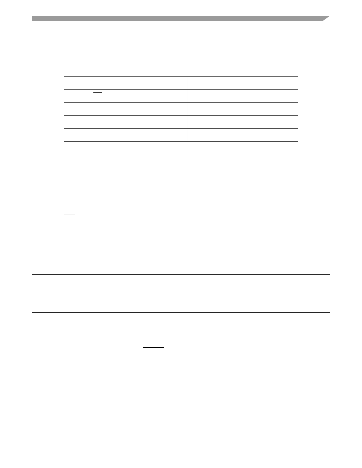
• The word “assert” means that a high true (active high) signal is pulled high to VCC or that a low
true (active low) signal is pulled low to ground. The word “deassert” means that a high true signal
is pulled low to ground or that a low true signal is pulled high to VCC.
High True/Low True Signal Conventions
Signal/Symbol Logic State Signal State Voltage
1
PIN
PIN False Deasserted V
PIN True Asserted V
PIN False Deasserted Ground
1
PIN is a generic term for any pin on the chip.
2
Ground is an acceptable low voltage level. See the appropriate data sheet for the range of
acceptable low voltage levels (typically a TTL logic low).
3
VCC is an acceptable high voltage level. See the appropriate data sheet for the range of acceptable
high voltage levels (typically a TTL logic high).
True Asserted Ground
CC
CC
2
3
• Pins or signals that are asserted low (made active when pulled to ground)
— In text, have an overbar (e.g., RESET is asserted low).
— In code examples, have a tilde in front of their names. In example below, line 3 refers to the
SS0 pin (shown as ~SS0).
• Sets of pins or signals are indicated by the first and last pins or signals in the set (e.g., HA1–HA8).
• Code examples are displayed in a monospaced font, as shown below:
Example Sample Code Listing
BFSET #$0007,X:PCC Configure: line 1
; MISO0, MOSI0, SCK0 for SPI master line 2
; ~SS0 as PC3 for GPIO line 3
• Hex values are indicated with a dollar sign ($) preceding the hex value, as follows: $FFFFFF is the
X memory address for the core interrupt priority register (IPR-C).
• The word “reset” is used in four different contexts in this manual:
— the reset signal, written as “RESET,”
— the reset instruction, written as “RESET,”
— the reset operating state, written as “Reset,” and
— the reset function, written as “reset.”
DSP56366 24-Bit Digital Signal Processor User Manual, Rev. 4
Freescale Semiconductor iii
Page 24

NOTES
DSP56366 24-Bit Digital Signal Processor User Manual, Rev. 4
iv Freescale Semiconductor
Page 25
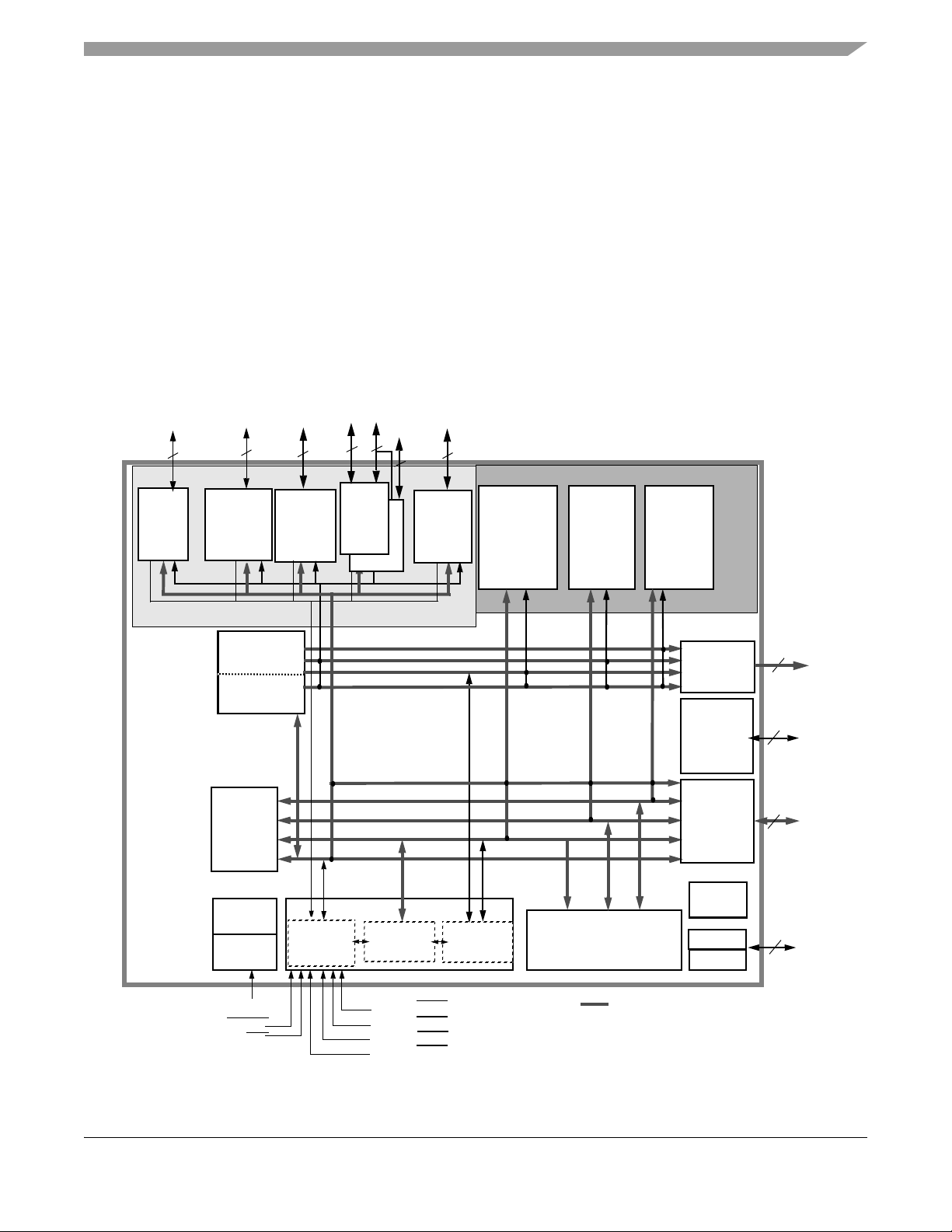
1 DSP56366 Overview
1.1 Introduction
This manual describes the DSP56366 24-bit digital signal processor (DSP), its memory, operating modes,
and peripheral modules. The DSP56366 is a member of the DSP56300 family of programmable CMOS
DSPs. The DSP56366 is targeted to applications that require digital audio compression/decompression,
sound field processing, acoustic equalization and other digital audio algorithms. Changes in core
functionality specific to the DSP56366 are also described in this manual. See Figure 1-1 for the block
diagram of the DSP56366.
4
8
6
ESAI
INTER-
FACE
ESAI_1
PERIPHERAL
EXPANSION AREA
INTER-
FACE
PIO_EB
24-BIT
DSP56300
Core
SHI
5
MEMORY EXPANSION AREA
PM_EB
YAB
XAB
PAB
DAB
X MEMORY
13K X 24
32K x 24
PROGRAM
RAM
/INSTR.
CACHE
3K x 24
PROGRAM
ROM
40K x 24
Bootstrap
DDB
YDB
XDB
PDB
GDB
RAM
ROM
XM_EB
Y MEMORY
RAM
7K X 24
ROM
8K x 24
YM_EB
EXTERNAL
ADDRESS
SWITCH
DRAM &
SRAM BUS
INTERFACE
I - CACHE
EXTERNAL
DATA BUS
BUS
&
SWITCH
18
ADDRESS
10
CONTROL
24
DATA
TRIPLE
TIMER
1
2
DAX
(SPDIF Tx.)
INTER-FAC
E
ADDRESS
GENERATION
UNIT
SIX CHANNELS
DMA UNIT
INTERNAL
DATA
BUS
16
HOST
INTER-
FAC E
POWER
PLL
CLOCK
GENERATO
EXTAL
RESET
PINIT/NMI
PROGRAM
INTERRUPT
CONTROLLER
PROGRAM
DECODE
CONTROLLE
MODA/IRQA
MODB/IRQB
MODC/IRQC
PROGRAM
ADDRESS
GENERATOR
DATA ALU
24X24+56->56-BIT MAC
TWO 56-BIT ACCUMULATORS
BARREL SHIFTER
24 BITS BUS
MNGMNT
JTAG
OnCE™
4
MODD/IRQD
Figure 1-1 DSP56366 Block Diagram
DSP56366 24-Bit Digital Signal Processor User Manual, Rev. 4
Freescale Semiconductor 1-1
Page 26

DSP56300 Core Description
1.2 DSP56300 Core Description
The DSP56366 uses the DSP56300 core, a high-performance, single clock cycle per instruction engine that
provides up to twice the performance of Freescale's popular DSP56000 core family while retaining code
compatibility with it.
The DSP56300 core family offers a new level of performance in speed and power, provided by its rich
instruction set and low power dissipation, thus enabling a new generation of wireless, telecommunications,
and multimedia products. For a description of the DSP56300 core, see Section 1.4, "DSP56300 Core
Functional Blocks". Significant architectural enhancements to the DSP56300 core family include a barrel
shifter, 24-bit addressing, an instruction cache, and direct memory access (DMA).
The DSP56300 core family members contain the DSP56300 core and additional modules. The modules
are chosen from a library of standard predesigned elements such as memories and peripherals. New
modules may be added to the library to meet customer specifications. A standard interface between the
DSP56300 core and the on-chip memory and peripherals supports a wide variety of memory and
peripheral configurations. Refer to Section 3, "Memory Configuration".
Core features are described fully in the DSP56300 Family Manual. Pinout, memory, and peripheral
features are described in this manual.
• DSP56300 modular chassis
— 120 Million Instructions Per Second (MIPS) with an 120 MHz clock at 3.3V.
— Object Code Compatible with the 56K core.
— Data ALU with a 24 × 24 bit multiplier-accumulator and a 56-bit barrel shifter. 16-bit
arithmetic support.
— Program Control with position independent code support and instruction cache support.
— Six-channel DMA controller.
— PLL based clocking with a wide range of frequency multiplications (1 to 4096), predivider
factors (1 to 16) and power saving clock divider (2i: i=0 to 7). Reduces clock noise.
— Internal address tracing support and OnCE™ for Hardware/Software debugging.
— JTAG port.
— Very low-power CMOS design, fully static design with operating frequencies down to DC.
— STOP and WAIT low-power standby modes.
• On-chip Memory Configuration
—7K × 24 Bit Y-Data RAM and 8K × 24 Bit Y-Data ROM.
— 13K × 24 Bit X-Data RAM and 32K × 24 Bit X-Data ROM.
— 40K × 24 Bit Program ROM.
—3K × 24 Bit Program RAM and 192 × 24 Bit Bootstrap ROM. 1K of Program RAM may be
used as Instruction Cache or for Program ROM patching.
—2K × 24 Bit from Y Data RAM and 5K × 24 Bit from X Data RAM can be switched to Program
RAM resulting in up to 10K × 24 Bit of Program RAM.
• Off-chip memory expansion
— External Memory Expansion Port.
DSP56366 24-Bit Digital Signal Processor User Manual, Rev. 4
1-2 Freescale Semiconductor
Page 27

DSP56366 Audio Processor Architecture
— Off-chip expansion up to two 16M × 24-bit word of Data memory.
— Off-chip expansion up to 16M × 24-bit word of Program memory.
— Simultaneous glueless interface to SRAM and DRAM.
• Peripheral modules
— Serial Audio Interface (ESAI): up to 4 receivers and up to 6 transmitters, master or slave. I
Sony, AC97, network and other programmable protocols.
— Serial Audio Interface I (ESAI_1): up to 4 receivers and up to 6 transmitters, master or slave.
2
I
S, Sony, AC97, network and other programmable protocols
The ESAI_1 shares four of the data pins with ESAI, and ESAI_1 does NOT support HCKR and
HCKT (high frequency clocks)
— Serial Host Interface (SHI): SPI and I2C protocols, multi master capability, 10-word receive
FIFO, support for 8, 16 and 24-bit words.
— Byte-wide parallel Host Interface (HDI08) with DMA support.
— Triple Timer module (TEC).
— Digital Audio Transmitter (DAX): 1 serial transmitter capable of supporting the SPDIF,
IEC958, CP-340 and AES/EBU digital audio formats.
— Pins of unused peripherals (except SHI) may be programmed as GPIO lines.
• 144-pin plastic TQFP package.
2
S,
1.3 DSP56366 Audio Processor Architecture
This section defines the DSP56366 audio processor architecture. The audio processor is composed of the
following units:
• The DSP56300 core is composed of the Data ALU, Address Generation Unit, Program Controller,
Instruction-Cache Controller, DMA Controller, PLL-based clock oscillator, Memory Module
Interface, Peripheral Module Interface and the On-Chip Emulator (OnCE). The DSP56300 core is
described in the document DSP56300 24-Bit Digital Signal Processor Family Manual, Freescale
publication DSP56300FM.
• Memory modules.
• Peripheral modules. The peripheral modules are defined in the following sections.
Memory sizes in the block diagram are defaults. Memory may be differently partitioned, according to the
memory mode of the chip. See Section 1.4.8, "On-Chip Memory" for more details about memory size.
1.4 DSP56300 Core Functional Blocks
The DSP56300 core provides the following functional blocks:
• Data arithmetic logic unit (Data ALU)
• Address generation unit (AGU)
• Program control unit (PCU)
• Bus interface unit (BIU)
• DMA controller (with six channels)
DSP56366 24-Bit Digital Signal Processor User Manual, Rev. 4
Freescale Semiconductor 1-3
Page 28

DSP56300 Core Functional Blocks
• Instruction cache controller
• PLL-based clock oscillator
• OnCE module
• JTAG TAP
• Memory
In addition, the DSP56366 provides a set of on-chip peripherals, described in Section 1.5, "Peripheral
Overview".
1.4.1 Data ALU
The Data ALU performs all the arithmetic and logical operations on data operands in the DSP56300 core.
The components of the Data ALU are as follows:
• Fully pipelined 24-bit × 24-bit parallel multiplier-accumulator (MAC)
• Bit field unit, comprising a 56-bit parallel barrel shifter (fast shift and normalization; bit stream
generation and parsing)
• Conditional ALU instructions
• 24-bit or 16-bit arithmetic support under software control
• Four 24-bit input general purpose registers: X1, X0, Y1, and Y0
• Six Data ALU registers (A2, A1, A0, B2, B1, and B0) that are concatenated into two general
purpose, 56-bit accumulators (A and B), accumulator shifters
• Two data bus shifter/limiter circuits
1.4.1.1 Data ALU Registers
The Data ALU registers can be read or written over the X memory data bus (XDB) and the Y memory data
bus (YDB) as 24- or 48-bit operands (or as 16- or 32-bit operands in 16-bit arithmetic mode). The source
operands for the Data ALU, which can be 24, 48, or 56 bits (16, 32, or 40 bits in 16-bit arithmetic mode),
always originate from Data ALU registers. The results of all Data ALU operations are stored in an
accumulator.
All the Data ALU operations are performed in two clock cycles in pipeline fashion so that a new
instruction can be initiated in every clock, yielding an effective execution rate of one instruction per clock
cycle. The destination of every arithmetic operation can be used as a source operand for the immediately
following arithmetic operation without a time penalty (i.e., without a pipeline stall).
1.4.1.2 Multiplier-Accumulator (MAC)
The MAC unit comprises the main arithmetic processing unit of the DSP56300 core and performs all of
the calculations on data operands. In the case of arithmetic instructions, the unit accepts as many as three
input operands and outputs one 56-bit result of the following form- Extension:Most Significant
Product:Least Significant Product (EXT:MSP:LSP).
The multiplier executes 24-bit × 24-bit, parallel, fractional multiplies, between two’s-complement signed,
unsigned, or mixed operands. The 48-bit product is right-justified and added to the 56-bit contents of either
DSP56366 24-Bit Digital Signal Processor User Manual, Rev. 4
1-4 Freescale Semiconductor
Page 29

DSP56300 Core Functional Blocks
the A or B accumulator. A 56-bit result can be stored as a 24-bit operand. The LSP can either be truncated
or rounded into the MSP. Rounding is performed if specified.
1.4.2 Address Generation Unit (AGU)
The AGU performs the effective address calculations using integer arithmetic necessary to address data
operands in memory and contains the registers used to generate the addresses. It implements four types of
arithmetic: linear, modulo, multiple wrap-around modulo, and reverse-carry. The AGU operates in parallel
with other chip resources to minimize address-generation overhead.
The AGU is divided into two halves, each with its own Address ALU. Each Address ALU has four sets of
register triplets, and each register triplet is composed of an address register, an offset register, and a
modifier register. The two Address ALUs are identical. Each contains a 24-bit full adder (called an offset
adder).
A second full adder (called a modulo adder) adds the summed result of the first full adder to a modulo
value that is stored in its respective modifier register. A third full adder (called a reverse-carry adder) is
also provided.
The offset adder and the reverse-carry adder are in parallel and share common inputs. The only difference
between them is that the carry propagates in opposite directions. Test logic determines which of the three
summed results of the full adders is output.
Each Address ALU can update one address register from its respective address register file during one
instruction cycle. The contents of the associated modifier register specifies the type of arithmetic to be used
in the address register update calculation. The modifier value is decoded in the Address ALU.
1.4.3 Program Control Unit (PCU)
The PCU performs instruction prefetch, instruction decoding, hardware DO loop control, and exception
processing. The PCU implements a seven-stage pipeline and controls the different processing states of the
DSP56300 core. The PCU consists of the following three hardware blocks:
• Program decode controller (PDC)
• Program address generator (PAG)
• Program interrupt controller (PIC)
The PDC decodes the 24-bit instruction loaded into the instruction latch and generates all signals necessary
for pipeline control. The PAG contains all the hardware needed for program address generation, system
stack, and loop control. The PIC arbitrates among all interrupt requests (internal interrupts, as well as the
five external requests: IRQA, IRQB, IRQC, IRQD, and NMI), and generates the appropriate interrupt
vector address.
PCU features include the following:
• Position independent code support
• Addressing modes optimized for DSP applications (including immediate offsets)
• On-chip instruction cache controller
• On-chip memory-expandable hardware stack
DSP56366 24-Bit Digital Signal Processor User Manual, Rev. 4
Freescale Semiconductor 1-5
Page 30

DSP56300 Core Functional Blocks
• Nested hardware DO loops
• Fast auto-return interrupts
The PCU implements its functions using the following registers:
• PC—program counter register
• SR—Status register
• LA—loop address register
• LC—loop counter register
• VBA—vector base address register
• SZ—stack size register
• SP—stack pointer
• OMR—operating mode register
• SC—stack counter register
The PCU also includes a hardware system stack (SS).
1.4.4 Internal Buses
To provide data exchange between blocks, the following buses are implemented:
• Peripheral input/output expansion bus (PIO_EB) to peripherals
• Program memory expansion bus (PM_EB) to program memory
• X memory expansion bus (XM_EB) to X memory
• Y memory expansion bus (YM_EB) to Y memory
• Global data bus (GDB) between registers in the DMA, AGU, OnCE, PLL, BIU, and PCU as well
as the memory-mapped registers in the peripherals
• DMA data bus (DDB) for carrying DMA data between memories and/or peripherals
• DMA address bus (DAB) for carrying DMA addresses to memories and peripherals
• Program Data Bus (PDB) for carrying program data throughout the core
• X memory Data Bus (XDB) for carrying X data throughout the core
• Y memory Data Bus (YDB) for carrying Y data throughout the core
• Program address bus (PAB) for carrying program memory addresses throughout the core
• X memory address bus (XAB) for carrying X memory addresses throughout the core
• Y memory address bus (YAB) for carrying Y memory addresses throughout the core
All internal buses on the DSP56300 family members are 24-bit buses. See Figure 1-1.
1.4.5 Direct Memory Access (DMA)
The DMA block has the following features:
• Six DMA channels supporting internal and external accesses
• One-, two-, and three-dimensional transfers (including circular buffering)
DSP56366 24-Bit Digital Signal Processor User Manual, Rev. 4
1-6 Freescale Semiconductor
Page 31

DSP56300 Core Functional Blocks
• End-of-block-transfer interrupts
• Triggering from interrupt lines and all peripherals
1.4.6 PLL-based Clock Oscillator
The clock generator in the DSP56300 core is composed of two main blocks: the PLL, which performs
clock input division, frequency multiplication, and skew elimination; and the clock generator (CLKGEN),
which performs low-power division and clock pulse generation. PLL-based clocking:
• Allows change of low-power divide factor (DF) without loss of lock
• Provides output clock with skew elimination
• Provides a wide range of frequency multiplications (1 to 4096), predivider factors (1 to 16), and a
power-saving clock divider (2i: i = 0 to 7) to reduce clock noise
The PLL allows the processor to operate at a high internal clock frequency using a low frequency clock
input. This feature offers two immediate benefits:
• A lower frequency clock input reduces the overall electromagnetic interference generated by a
system.
• The ability to oscillate at different frequencies reduces costs by eliminating the need to add
additional oscillators to a system.
1.4.7 JTAG TAP and OnCE Module
The DSP56300 core provides a dedicated user-accessible TAP fully compatible with the IEEE 1149.1
Standard Test Access Port and Boundary Scan Architecture
. Problems associated with testing high-density
circuit boards led to developing this standard under the sponsorship of the Test Technology Committee of
IEEE and JTAG. The DSP56300 core implementation supports circuit-board test strategies based on this
standard.
The test logic includes a TAP consisting of four dedicated signals, a 16-state controller, and three test data
registers. A boundary scan register links all device signals into a single shift register. The test logic,
implemented utilizing static logic design, is independent of the device system logic. More information on
the JTAG port is provided in DSP56300 Family Manual, JTAG Port.
The OnCE module provides a nonintrusive means of interacting with the DSP56300 core and its
peripherals so a user can examine registers, memory, or on-chip peripherals. This facilitates hardware and
software development on the DSP56300 core processor. OnCE module functions are provided through the
JTAG TAP signals. More information on the OnCE module is provided in DSP56300 Family Manual,
On-Chip Emulation Module
.
1.4.8 On-Chip Memory
The memory space of the DSP56300 core is partitioned into program memory space,
X data memory space, and Y data memory space. The data memory space is divided into X and Y data
memory in order to work with the two Address ALUs and to feed two operands simultaneously to the Data
DSP56366 24-Bit Digital Signal Processor User Manual, Rev. 4
Freescale Semiconductor 1-7
Page 32

Peripheral Overview
ALU. Memory space includes internal RAM and ROM and can be expanded off-chip under software
control.
There is an instruction cache, made using program RAM. The patch mode (which uses instruction cache
space) is used to patch program ROM. The memory switch mode is used to increase the size of program
RAM as needed (switch from X data RAM and/or Y data RAM).
There are on-chip ROMs for program memory (40K × 24-bit), bootstrap memory (192 words × 24-bit), X
ROM (32K × 24-bit), and Y ROM(8K × 24-bit).
More information on the internal memory is provided in Section 3, "Memory Configuration".
1.4.9 Off-Chip Memory Expansion
Memory can be expanded off-chip as follows:
• Data memory can be expanded to two 16 M × 24-bit word memory spaces in 24-bit address mode
(64K in 16-bit address mode).
• Program memory can be expanded to one 16 M × 24-bit word memory space in 24-bit address
mode (64K in 16-bit address mode).
Other features of external memory expansion include the following:
• External memory expansion port
• Chip-select logic glueless interface to static random access memory (SRAM)
• On-chip dynamic RAM (DRAM) controller for glueless interface to DRAM
• Eighteen external address lines
1.5 Peripheral Overview
The DSP56366 is designed to perform a wide variety of fixed-point digital signal processing functions. In
addition to the core features previously discussed, the DSP56366 provides the following peripherals:
• 8-bit parallel host interface (HDI08, with DMA support) to external hosts
• As many as 37 user-configurable general purpose input/output (GPIO) signals
• Timer/event counter (TEC) module, containing three independent timers
• Memory switch mode in on-chip memory
• Four external interrupt/mode control lines and one external non-maskable interrupt line
• Enhanced serial audio interface (ESAI) with up to four receivers and up to six transmitters, master
or slave, using the I
• A second enhanced serial audio interface (ESAI_1) with 6 dedicated pins.
• Serial host interface (SHI) using SPI and I
receive FIFO, and support for 8-, 16-, and 24-bit words
• Digital audio transmitter (DAX): a serial transmitter capable of supporting the SPDIF, IEC958,
CP-340, and AES/EBU digital audio formats
2
S, Sony, AC97, network, and other programmable protocols
2
C protocols, with multi-master capability, 10-word
DSP56366 24-Bit Digital Signal Processor User Manual, Rev. 4
1-8 Freescale Semiconductor
Page 33

Peripheral Overview
1.5.1 Host Interface (HDI08)
The host interface (HDI08) is a byte-wide, full-duplex, double-buffered, parallel port that can be connected
directly to the data bus of a host processor. The HDI08 supports a variety of buses and provides glueless
connection with a number of industry-standard DSPs, microcomputers, microprocessors, and DMA
hardware.
The DSP core treats the HDI08 as a memory-mapped peripheral, using either standard polled or interrupt
programming techniques. Separate transmit and receive data registers are double-buffered to allow the
DSP and host processor to efficiently transfer data at high speed. Memory mapping allows DSP core
communication with the HDI08 registers to be accomplished using standard instructions and addressing
modes.
Since the host bus may operate asynchronously with the DSP core clock, the HDI08 registers are divided
into 2 banks. The “host side” bank is accessible to the external host, and the “DSP side” bank is accessible
to the DSP core.
The HDI08 supports the following three classes of interfaces:
• Host processor/MCU connection
• DMA controller
• GPIO port
Host port pins not in use may be configured as GPIO pins. The host interface provides up to 16 GPIO pins.
These pins can be programmed to function as either GPIO or host interface.
For more information on the HDI08, see Section 6, Host Interface (HDI08).
1.5.2 General Purpose Input/Output (GPIO)
The GPIO port consists of as many as 37 programmable signals, all of which are also used by the
peripherals (HDI08, ESAI, ESAI_1, DAX, and TEC). There are no dedicated GPIO signals. The signals
are configured as GPIO after hardware reset. Register programming techniques for all GPIO functionality
among these interfaces are very similar.
1.5.3 Triple Timer (TEC)
This section describes a peripheral module composed of a common 21-bit prescaler and three independent
and identical general purpose 24-bit timer/event counters, each one having its own register set.
Each timer can use internal or external clocking and can interrupt the DSP after a specified number of
events (clocks). Timer 0 can signal an external device after counting internal events. Each timer can also
be used to trigger DMA transfers after a specified number of events (clocks) occurred. One timer (Timer
0) connects to the external world through one bidirectional pin TIO0. When TIO0 is configured as input,
the timer functions as an external event counter or can measure external pulse width/signal period. When
TIO0 is used as output the timer is functioning as either a timer, a watchdog or a Pulse Width Modulator.
When the TIO0 pin is not used by the timer it can be used as a General Purpose Input/Output Pin. Refer
to Section 11, "Timer/ Event Counter".
DSP56366 24-Bit Digital Signal Processor User Manual, Rev. 4
Freescale Semiconductor 1-9
Page 34

Peripheral Overview
1.5.4 Enhanced Serial Audio Interface (ESAI)
The ESAI provides a full-duplex serial port for serial communication with a variety of serial devices
including one or more industry-standard codecs, other DSPs, microprocessors, and peripherals that
implement the Freescale SPI serial protocol. The ESAI consists of independent transmitter and receiver
sections, each with its own clock generator. It is a superset of the DSP56300 family ESSI peripheral and
of the DSP56000 family SAI peripheral. For more information on the ESAI, refer to Section 8, "Enhanced
Serial AUDIO Interface (ESAI)".
1.5.5 Enhanced Serial Audio Interface 1 (ESAI_1)
The ESAI_1 is a second ESAI interface with just 6 dedicated pins instead of the 12 pins of the full ESAI.
Four data pins are shared with the ESAI, while the two high frequency clock pins are not available. Other
than the available pins, ESAI_1 is functionally identical to ESAI. For more information on the ESAI_1,
refer to Section 9, "Enhanced Serial Audio Interface 1 (ESAI_1)".
1.5.6 Serial Host Interface (SHI)
The SHI is a serial input/output interface providing a path for communication and program/coefficient data
transfers between the DSP and an external host processor. The SHI can also communicate with other serial
peripheral devices. The SHI can interface directly to either of two well-known and widely used
synchronous serial buses: the Freescale serial peripheral interface (SPI) bus and the Philips
inter-integrated-circuit control (I2C) bus. The SHI supports either the SPI or I2C bus protocol, as required,
from a slave or a single-master device. To minimize DSP overhead, the SHI supports single-, double-, and
triple-byte data transfers. The SHI has a 10-word receive FIFO that permits receiving up to 30 bytes before
generating a receive interrupt, reducing the overhead for data reception. For more information on the SHI,
refer to Section 7, "Serial Host Interface".
1.5.7 Digital Audio Transmitter (DAX)
The DAX is a serial audio interface module that outputs digital audio data in the AES/EBU, CP-340 and
IEC958 formats. For more information on the DAX, refer to Section 10, "Digital Audio Transmitter".
DSP56366 24-Bit Digital Signal Processor User Manual, Rev. 4
1-10 Freescale Semiconductor
Page 35

2 Signal/Connection Descriptions
2.1 Signal Groupings
The input and output signals of the DSP56364 are organized into functional groups, which are listed in
Table 2-1 and illustrated in Figure 2-1.
The DSP56364 is operated from a 3.3 V supply; however, some of the inputs can tolerate 5 V. A special
notice for this feature is added to the signal descriptions of those inputs.
Table 2-1 DSP56364 Functional Signal Groupings
Functional Group
Power (V
Ground (GND) 18 Table 2-3
Clock and PLL 3 Table 2-4
Address bus
Data bus 24 Tab le 2-6
Bus control 10 Tab le 2-7
Interrupt and mode control 5 Table 2-8
HDI08 Port B
SHI 5 Table 2-10
ESAI Port C
ESAI_1 Port E
Digital audio transmitter (DAX) Port D
)20Table 2-2
CC
1
Por t A
2
3
4
5
Number of
Signals
18
16 Tab le 2-9
12
6
2
Detailed
Description
Table 2-5
Table 2-11
Table 2-12
Table 2-13
Timer 1 Table 2-14
JTAG/OnCE Port 4 Table 2-15
1
Port A is the external memory interface port, including the external address bus, data bus, and control signals.
2
Port B signals are the GPIO port signals which are multiplexed with the HDI08 signals.
3
Port C signals are the GPIO port signals which are multiplexed with the ESAI signals.
4
Port E signals are the GPIO port signals which are multiplexed with the ESAI_1 signals.
5
Port D signals are the GPIO port signals which are multiplexed with the DAX signals.
DSP56366 24-Bit Digital Signal Processor User Manual, Rev. 4
Freescale Semiconductor 2-1
Page 36

Signal Groupings
PORT A ADDRESS BUS
A0-A17
VCCA (3)
GNDA (4)
PORT A DATA BUS
D0-D23
VCCD (4)
GNDD (4)
PORT A BUS CONTROL
AA0-AA2/RAS0-RAS2
CAS
VCCC (2)
GNDC (2)
INTERRUPT AND
MODE CONTROL
MODA/IRQA
MODB/IRQB
MODC/IRQC
MODD/IRQD
RESET
PLL AND CLOCK
EXTAL
PINIT/NMI
PCAP
VCCP
GNDP
QUIET POWER
VCCQH (3)
VCCQL (4)
GNDQ (4)
SPDIF TRANSMITTER (DAX)
ADO [PD1]
ACI [PD0]
TIMER 0
TIO0 [TIO0]
RD
WR
TA
BR
BG
BB
DSP56366
Port D
Port B
Port C
Port E
OnCE
‰
ON-CHIP EMULATION/
TDI
TCK
TDO
TMS
JTAG PORT
PARALLEL HOST PORT (HDI08)
HAD(7:0) [PB0-PB7]
HAS/HA0 [PB8]
HA8/HA1 [PB9]
HA9/HA2 [PB10]
HRW/HRD [PB11]
HDS/HWR [PB12]
HCS/HA10 [PB13]
HOREQ/HTRQ [PB14]
HACK/HRRQ [PB15]
VCCH
GNDH
SERIAL AUDIO INTERFACE (ESAI)
SCKT[PC3]
FST [PC4]
HCKT [PC5]
SCKR [PC0]
FSR [PC1]
HCKR [PC2]
SDO0 [PC11] / SDO0_1[PE11]
SDO1 [PC10] / SDO1_1[PE10]
SDO2/SDI3[PC9] / SDO2_1/SDI3_1[PE9]
SDO3/SDI2[PC8] / SDO3_1/SDI2_1[PE8]
SDO4/SDI1 [PC7]
SDO5/SDI0 [PC6]
SERIAL AUDIO INTERFACE(ESAI_1)
SCKT_1[PE3]
FS
T_1[PE4]
SCKR_1[PE0]
FSR_1[PE1]
SDO4_1/SDI1_1[PE7]
SDO5_1/SDI0_1[PE6]
VCCS (2)
GNDS (2)
SERIAL HOST INTERFACE (SHI)
MOSI/HA0
/HA2
SS
MISO/SDA
SCK/SCL
HREQ
Figure 2-1 Signals Identified by Functional Group
DSP56366 24-Bit Digital Signal Processor User Manual, Rev. 4
2-2 Freescale Semiconductor
Page 37

2.2 Power
Table 2-2 Power Inputs
Power Name Description
Power
V
CCP
PLL Power — V
CCP
should be provided with an extremely low impedance path to the V
input.
V
(4) Quiet Core (Low) Power — V
CCQL
must be tied externally to all other chip power inputs. The user must provide adequate external
decoupling capacitors. There are four V
(3) Quiet External (High) Power — V
V
CCQH
externally to all other chip power inputs. The user must provide adequate decoupling capacitors. There
are three V
V
(3) Address Bus Power — V
CCA
CCQH
inputs.
must be tied externally to all other chip power inputs. The user must provide adequate external
decoupling capacitors. There are three V
(4) Data Bus Power — V
V
CCD
be tied externally to all other chip power inputs. The user must provide adequate external decoupling
capacitors. There are four V
(2) Bus Control Power — V
V
CCC
externally to all other chip power inputs. The user must provide adequate external decoupling
capacitors. There are two V
V
CCH
Host Power — V
CCH
to all other chip power inputs. The user must provide adequate external decoupling capacitors. There
is one V
CCH
input.
is VCC dedicated for PLL use. The voltage should be well-regulated and the input
power rail. There is one V
CC
is an isolated power for the internal processing logic. This input
CCQL
inputs.
CCQL
is a quiet power source for I/O lines. This input must be tied
CCQH
is an isolated power for sections of the address bus I/O drivers. This input
CCA
inputs.
CCA
is an isolated power for sections of the data bus I/O drivers. This input must
CCD
inputs.
CCD
is an isolated power for the bus control I/O drivers. This input must be tied
CCC
inputs.
CCC
CCP
is an isolated power for the HDI08 I/O drivers. This input must be tied externally
(2) SHI, ESAI, ESAI_1, DAX and Timer Power — V
V
CCS
is an isolated power for the SHI, ESAI, ESAI_1,
CCS
DAX and Timer. This input must be tied externally to all other chip power inputs. The user must provide
adequate external decoupling capacitors. There are two V
CCS
inputs.
2.3 Ground
Table 2-3 Grounds
Ground Name Description
GND
P
(4) Quiet Ground — GNDQ is an isolated ground for the internal processing logic. This connection must
GND
Q
Freescale Semiconductor 2-3
PLL Ground — GNDP is a ground dedicated for PLL use. The connection should be provided with an
extremely low-impedance path to ground. V
located as close as possible to the chip package. There is one GND
should be bypassed to GNDP by a 0.47 µF capacitor
CCP
connection.
P
be tied externally to all other chip ground connections. The user must provide adequate external
decoupling capacitors. There are four GND
connections.
Q
DSP56366 24-Bit Digital Signal Processor User Manual, Rev. 4
Page 38

Clock and PLL
Table 2-3 Grounds (continued)
Ground Name Description
GNDA (4) Address Bus Ground — GNDA is an isolated ground for sections of the address bus I/O drivers. This
connection must be tied externally to all other chip ground connections. The user must provide
adequate external decoupling capacitors. There are four GND
(4) Data Bus Ground — GNDD is an isolated ground for sections of the data bus I/O drivers. This
GND
D
connection must be tied externally to all other chip ground connections. The user must provide
adequate external decoupling capacitors. There are four GND
GNDC (2) Bus Control Ground — GNDC is an isolated ground for the bus control I/O drivers. This connection
must be tied externally to all other chip ground connections. The user must provide adequate external
decoupling capacitors. There are two GND
connections.
C
connections.
A
connections.
D
GND
H
Host Ground — GNDh is an isolated ground for the HD08 I/O drivers. This connection must be tied
externally to all other chip ground connections. The user must provide adequate external decoupling
capacitors. There is one GND
(2) SHI, ESAI, ESAI_1, DAX and Timer Ground — GNDS is an isolated ground for the SHI, ESAI, ESAI_1,
GND
S
connection.
H
DAX and Timer. This connection must be tied externally to all other chip ground connections. The user
must provide adequate external decoupling capacitors. There are two GND
connections.
S
2.4 Clock and PLL
Table 2-4 Clock and PLL Signals
Signal
Name
Typ e
EXTAL Input Input External Clock Input — An external clock source must be connected to EXTAL
PCAP Input Input PLL Capacitor — PCAP is an input connecting an off-chip capacitor to the PLL
PINIT/NMI
Input Input PLL Initial/Nonmaskable Interrupt — During assertion of RESET, the value of
State during
Reset
Signal Description
in order to supply the clock to the internal clock generator and PLL.
This input cannot tolerate 5 V.
filter. Connect one capacitor terminal to PCAP and the other terminal to V
If the PLL is not used, PCAP may be tied to V
PINIT/NMI
is written into the PLL Enable (PEN) bit of the PLL control register,
determining whether the PLL is enabled or disabled. After RESET
and during normal instruction processing, the PINIT/NMI
, GND, or left floating.
CC
Schmitt-trigger input
de assertion
is a negative-edge-triggered nonmaskable interrupt (NMI) request internally
synchronized to internal system clock.
This input cannot tolerate 5 V.
CCP
.
DSP56366 24-Bit Digital Signal Processor User Manual, Rev. 4
2-4 Freescale Semiconductor
Page 39

External Memory Expansion Port (Port A)
2.5 External Memory Expansion Port (Port A)
When the DSP56364 enters a low-power standby mode (stop or wait), it releases bus mastership and
tri-states the relevant port A signals: A0 – A17, D0 – D23, AA0/RAS0 – AA2/RAS2, RD, WR, BB, CAS.
2.5.1 External Address Bus
Table 2-5 External Address Bus Signals
Signal Name Type
A0–A17 Output Tri-stated Address Bus — When the DSP is the bus master, A0 – A17 are active-high
State during
Reset
Signal Description
outputs that specify the address for external program and data memory
accesses. Otherwise, the signals are tri-stated. To minimize power dissipation,
A0 – A17 do not change state when external memory spaces are not being
accessed.
2.5.2 External Data Bus
Table 2-6 External Data Bus Signals
Signal Name Type State during Reset Signal Description
D0–D23 Input/Output Tri-stated Data Bus — When the DSP is the bus master,
D0 – D23 are active-high, bidirectional input/outputs that provide the
bidirectional data bus for external program and data memory
accesses. Otherwise,
D0 – D23 are tri-stated.
2.5.3 External Bus Control
Table 2-7 External Bus Control Signals
Signal Name Type
AA0–AA2/RAS0
– RAS2
CAS Output Tri-stated Column Address Strobe — When the DSP is the bus master, CAS is an
RD
Freescale Semiconductor 2-5
Output Tri-stated Address Attribute or Row Address Strobe — When defined as AA, these
Output Tri-stated Read Enable — When the DSP is the bus master, RD is an active-low output
State during
Reset
signals can be used as chip selects or additional address lines. When defined
as RAS
, these signals can be used as RAS for DRAM interface. These
signals are tri-statable outputs with programmable polarity.
active-low output used by DRAM to strobe the column address. Otherwise, if
the bus mastership enable (BME) bit in the DRAM control register is cleared,
the signal is tri-stated.
that is asserted to read external memory on the data bus (D0-D23).
Otherwise, RD
DSP56366 24-Bit Digital Signal Processor User Manual, Rev. 4
is tri-stated.
Signal Description
Page 40

External Memory Expansion Port (Port A)
Table 2-7 External Bus Control Signals (continued)
Signal Name Type
WR
TA
Output Tri-stated Write Enable — When the DSP is the bus master, WR is an active-low output
Input Ignored Input Transfer Acknowledge — If the DSP is the bus master and there is no
State during
Reset
Signal Description
that is asserted to write external memory on the data bus (D0-D23).
Otherwise, WR
external bus activity, or the DSP is not the bus master, the TA
The TA
input is a data transfer acknowledge (DTACK) function that can extend
an external bus cycle indefinitely. Any number of wait states (1, 2. . .infinity)
may be added to the wait states inserted by the BCR by keeping TA
deasserted. In typical operation, TA
is asserted to enable completion of the bus cycle, and is deasserted before
the next bus cycle. The current bus cycle completes one clock period after TA
is asserted synchronous to the internal system clock. The number of wait
states is determined by the TA
whichever is longer. The BCR can be used to set the minimum number of wait
states in external bus cycles.
In order to use the TA
one wait state. A zero wait state access cannot be extended by TA
deassertion, otherwise improper operation may result. TA
synchronously or asynchronously, depending on the setting of the TAS bit in
the operating mode register (OMR).
TA
functionality may not be used while performing DRAM type accesses,
otherwise improper operation may result.
is tri-stated.
input is ignored.
is deasserted at the start of a bus cycle,
input or by the bus control register (BCR),
functionality, the BCR must be programmed to at least
can operate
BR Output Output
(deasserted)
Bus Request — BR is an active-low output, never tri-stated. BR is asserted
when the DSP requests bus mastership. BR
longer needs the bus. BR
whether the DSP56364 is a bus master or a bus slave. Bus “parking” allows
BR
to be deasserted even though the DSP56364 is the bus master. (See the
description of bus “parking” in the BB
hold (BRH) bit in the BCR allows BR
even though the DSP does not need the bus. BR
external bus arbitrator that controls the priority, parking, and tenure of each
master on the same external bus. BR
external bus, never for the internal bus. During hardware reset, BR
deasserted and the arbitration is reset to the bus slave state.
may be asserted or deasserted independent of
is deasserted when the DSP no
signal description.) The bus request
to be asserted under software control
is typically sent to an
is only affected by DSP requests for the
is
DSP56366 24-Bit Digital Signal Processor User Manual, Rev. 4
2-6 Freescale Semiconductor
Page 41

Table 2-7 External Bus Control Signals (continued)
Interrupt and Mode Control
Signal Name Type
BG Input Ignored Input Bus Grant — BG is an active-low input. BG is asserted by an external bus
BB Input/
Output
State during
Reset
arbitration circuit when the DSP56364 becomes the next bus master. When
BG
is asserted, the DSP56364 must wait until BB is deasserted before taking
bus mastership. When BG
at the end of the current bus cycle. This may occur in the middle of an
instruction that requires more than one external bus cycle for execution.
For proper BG
in the OMR register must be set.
Input Bus Busy — BB is a bidirectional active-low input/output. BB indicates that
the bus is active. Only after BB
become the bus master (and then assert the signal again). The bus master
may keep BB
asserted or deasserted. This is called “bus parking” and allows the current
bus master to reuse the bus without rearbitration until another device requires
the bus. The deassertion of BB
is driven high and then released and held high by an external pull-up resistor).
For proper BB operation, the asynchronous bus arbitration enable bit (ABE)
in the OMR register must be set.
BB requires an external pull-up resistor.
operation, the asynchronous bus arbitration enable bit (ABE)
asserted after ceasing bus activity regardless of whether BR is
Signal Description
is deasserted, bus mastership is typically given up
is deasserted can the pending bus master
is done by an “active pull-up” method (i.e., BB
2.6 Interrupt and Mode Control
The interrupt and mode control signals select the chip’s operating mode as it comes out of hardware reset.
After RESET is deasserted, these inputs are hardware interrupt request lines.
DSP56366 24-Bit Digital Signal Processor User Manual, Rev. 4
Freescale Semiconductor 2-7
Page 42

Interrupt and Mode Control
Table 2-8 Interrupt and Mode Control
Signal Name Type
MODA/IRQA
MODB/IRQB
MODC/IRQC
Input Input Mode Select A/External Interrupt Request A — MODA/IRQA is an active-low
Input Input Mode Select B/External Interrupt Request B — MODB/IRQB is an active-low
Input Input Mode Select C/External Interrupt Request C — MODC/IRQC is an active-low
State during
Reset
Signal Description
Schmitt-trigger input, internally synchronized to the DSP clock. MODA/IRQA
selects the initial chip operating mode during hardware reset and becomes a
level-sensitive or negative-edge-triggered, maskable interrupt request input
during normal instruction processing. MODA, MODB, MODC, and MODD select
one of 16 initial chip operating modes, latched into the OMR when the RESET
signal is deasserted. If the processor is in the stop standby state and the
MODA/IRQA
This input is 5 V tolerant.
Schmitt-trigger input, internally synchronized to the DSP clock. MODB/IRQB
selects the initial chip operating mode during hardware reset and becomes a
level-sensitive or negative-edge-triggered, maskable interrupt request input
during normal instruction processing. MODA, MODB, MODC, and MODD select
one of 16 initial chip operating modes, latched into OMR when the RESET
signal is deasserted.
This input is 5 V tolerant.
Schmitt-trigger input, internally synchronized to the DSP clock. MODC/IRQC
selects the initial chip operating mode during hardware reset and becomes a
level-sensitive or negative-edge-triggered, maskable interrupt request input
during normal instruction processing. MODA, MODB, MODC, and MODD select
one of 16 initial chip operating modes, latched into OMR when the RESET
signal is deasserted.
This input is 5 V tolerant.
pin is pulled to GND, the processor will exit the stop state.
MODD/IRQD
RESET
2-8 Freescale Semiconductor
Input Input Mode Select D/External Interrupt Request D — MODD/IRQD is an active-low
Schmitt-trigger input, internally synchronized to the DSP clock. MODD/IRQD
selects the initial chip operating mode during hardware reset and becomes a
level-sensitive or negative-edge-triggered, maskable interrupt request input
during normal instruction processing. MODA, MODB, MODC, and MODD select
one of 16 initial chip operating modes, latched into OMR when the RESET
signal is deasserted.
This input is 5 V tolerant.
Input Input Reset — RESET is an active-low, Schmitt-trigger input. When asserted, the
chip is placed in the Reset state and the internal phase generator is reset. The
Schmitt-trigger input allows a slowly rising input (such as a capacitor charging)
to reset the chip reliably. When the RESET
operating mode is latched from the MODA, MODB, MODC, and MODD inputs.
The RESET
must be supplied while RESET is being asserted.
This input is 5 V tolerant.
DSP56366 24-Bit Digital Signal Processor User Manual, Rev. 4
signal must be asserted during power up. A stable EXTAL signal
signal is deasserted, the initial chip
Page 43

PARALLEL HOST INTERFACE (HDI08)
2.7 PARALLEL HOST INTERFACE (HDI08)
The HDI08 provides a fast, 8-bit, parallel data port that may be connected directly to the host bus. The
HDI08 supports a variety of standard buses and can be directly connected to a number of industry standard
microcomputers, microprocessors, DSPs, and DMA hardware.
Table 2-9 Host Interface
Signal Name Type
H0 – H7 Input/
output
HAD0 – HAD7 Input/
output
PB0 – PB7 Input, output, or
disconnected
HA0 Input GPIO
HAS/HAS Input Host Address Strobe — When HDI08 is programmed to interface a
State during
Reset
GPIO
disconnected
disconnected
Signal Description
Host Data — When HDI08 is programmed to interface a nonmultiplexed
host bus and the HI function is selected, these signals are lines 0 – 7 of the
bidirectional, tri-state data bus.
Host Address/Data — When HDI08 is programmed to interface a
multiplexed host bus and the HI function is selected, these signals are lines
0 – 7 of the address/data bidirectional, multiplexed, tri-state bus.
Port B 0–7 — When the HDI08 is configured as GPIO, these signals are
individually programmable as input, output, or internally disconnected.
The default state after reset for these signals is GPIO disconnected.
These inputs are 5 V tolerant.
Host Address Input 0 — When the HDI08 is programmed to interface a
nonmultiplexed host bus and the HI function is selected, this signal is line 0
of the host address input bus.
multiplexed host bus and the HI function is selected, this signal is the host
address strobe (HAS) Schmitt-trigger input. The polarity of the address
strobe is programmable, but is configured active-low (HAS
) following reset.
PB8 Input, output, or
disconnected
HA1 Input GPIO
disconnected
HA8 Input Host Address 8 — When HDI08 is programmed to interface a multiplexed
PB9 Input, output, or
disconnected
DSP56366 24-Bit Digital Signal Processor User Manual, Rev. 4
Freescale Semiconductor 2-9
Port B 8 — When the HDI08 is configured as GPIO, this signal is individually
programmed as input, output, or internally disconnected.
The default state after reset for this signal is GPIO disconnected.
This input is 5 V tolerant.
Host Address Input 1 — When the HDI08 is programmed to interface a
nonmultiplexed host bus and the HI function is selected, this signal is line 1
of the host address (HA1) input bus.
host bus and the HI function is selected, this signal is line 8 of the host
address (HA8) input bus.
Port B 9 — When the HDI08 is configured as GPIO, this signal is individually
programmed as input, output, or internally disconnected.
The default state after reset for this signal is GPIO disconnected.
This input is 5 V tolerant.
Page 44
PARALLEL HOST INTERFACE (HDI08)
Table 2-9 Host Interface (continued)
Signal Name Type
HA2 Input GPIO
HA9 Input Host Address 9 — When HDI08 is programmed to interface a multiplexed
PB10 Input, Output, or
Disconnected
HRW Input GPIO
HRD
HRD
/
Input Host Read Data — When HDI08 is programmed to interface a
State during
Reset
disconnected
disconnected
Signal Description
Host Address Input 2 — When the HDI08 is programmed to interface a
non-multiplexed host bus and the HI function is selected, this signal is line 2
of the host address (HA2) input bus.
host bus and the HI function is selected, this signal is line 9 of the host
address (HA9) input bus.
Port B 10 — When the HDI08 is configured as GPIO, this signal is
individually programmed as input, output, or internally disconnected.
The default state after reset for this signal is GPIO disconnected.
This input is 5 V tolerant.
Host Read/Write — When HDI08 is programmed to interface a
single-data-strobe host bus and the HI function is selected, this signal is the
Host Read/Write
double-data-strobe host bus and the HI function is selected, this signal is the
host read data strobe (HRD) Schmitt-trigger input. The polarity of the data
strobe is programmable, but is configured as active-low (HRD
(HRW) input.
) after reset.
PB11 Input, Output, or
Disconnected
/
HDS
HDS
HWR
/
HWR
PB12 Input, output, or
Input GPIO
Input Host Write Data — When HDI08 is programmed to interface a
disconnected
disconnected
Port B 11 — When the HDI08 is configured as GPIO, this signal is
individually programmed as input, output, or internally disconnected.
The default state after reset for this signal is GPIO disconnected.
This input is 5 V tolerant.
Host Data Strobe — When HDI08 is programmed to interface a
single-data-strobe host bus and the HI function is selected, this signal is the
host data strobe (HDS) Schmitt-trigger input. The polarity of the data strobe
is programmable, but is configured as active-low (HDS
double-data-strobe host bus and the HI function is selected, this signal is the
host write data strobe (HWR) Schmitt-trigger input. The polarity of the data
strobe is programmable, but is configured as active-low (HWR
reset.
Port B 12 — When the HDI08 is configured as GPIO, this signal is
individually programmed as input, output, or internally disconnected.
The default state after reset for this signal is GPIO disconnected.
This input is 5 V tolerant.
) following reset.
) following
DSP56366 24-Bit Digital Signal Processor User Manual, Rev. 4
2-10 Freescale Semiconductor
Page 45

Table 2-9 Host Interface (continued)
PARALLEL HOST INTERFACE (HDI08)
Signal Name Type
HCS Input GPIO
HA10 Input Host Address 10 — When HDI08 is programmed to interface a multiplexed
PB13 Input, output, or
disconnected
HOREQ
EQ
HTRQ/
HTRQ
/HOR
Output GPIO
Output Transmit Host Request — When HDI08 is programmed to interface a
State during
Reset
disconnected
disconnected
Signal Description
Host Chip Select — When HDI08 is programmed to interface a
nonmultiplexed host bus and the HI function is selected, this signal is the
host chip select (HCS) input. The polarity of the chip select is
programmable, but is configured active-low (HCS
host bus and the HI function is selected, this signal is line 10 of the host
address (HA10) input bus.
Port B 13 — When the HDI08 is configured as GPIO, this signal is
individually programmed as input, output, or internally disconnected.
The default state after reset for this signal is GPIO disconnected.
This input is 5 V tolerant.
Host Request — When HDI08 is programmed to interface a single host
request host bus and the HI function is selected, this signal is the host
request (HOREQ) output. The polarity of the host request is programmable,
but is configured as active-low (HOREQ
may be programmed as a driven or open-drain output.
double host request host bus and the HI function is selected, this signal is
the transmit host request (HTRQ) output. The polarity of the host request is
programmable, but is configured as active-low (HTRQ
host request may be programmed as a driven or open-drain output.
) following reset. The host request
) after reset.
) following reset. The
PB14 Input, output, or
disconnected
DSP56366 24-Bit Digital Signal Processor User Manual, Rev. 4
Port B 14 — When the HDI08 is configured as GPIO, this signal is
individually programmed as input, output, or internally disconnected.
The default state after reset for this signal is GPIO disconnected.
This input is 5 V tolerant.
Freescale Semiconductor 2-11
Page 46

Serial Host Interface
Table 2-9 Host Interface (continued)
Signal Name Type
HACK/
HACK
HRRQ/
HRRQ
PB15 Input, output, or
Input GPIO
Output Receive Host Request — When HDI08 is programmed to interface a
disconnected
State during
Reset
disconnected
Signal Description
Host Acknowledge — When HDI08 is programmed to interface a single
host request host bus and the HI function is selected, this signal is the host
acknowledge (HACK) Schmitt-trigger input. The polarity of the host
acknowledge is programmable, but is configured as active-low (HACK
reset.
double host request host bus and the HI function is selected, this signal is
the receive host request (HRRQ) output. The polarity of the host request is
programmable, but is configured as active-low (HRRQ
request may be programmed as a driven or open-drain output.
Port B 15 — When the HDI08 is configured as GPIO, this signal is
individually programmed as input, output, or internally disconnected.
The default state after reset for this signal is GPIO disconnected.
This input is 5 V tolerant.
) after reset. The host
) after
2.8 Serial Host Interface
The SHI has five I/O signals that can be configured to allow the SHI to operate in either SPI or I2C mode.
Table 2-10 Serial Host Interface Signals
Signal
Name
SCK Input or output Tri-stated SPI Serial Clock — The SCK signal is an output when the SPI is configured as
SCL Input or output I
Signal Type
State during
Reset
Signal Description
a master and a Schmitt-trigger input when the SPI is configured as a slave.
When the SPI is configured as a master, the SCK signal is derived from the
internal SHI clock generator. When the SPI is configured as a slave, the SCK
signal is an input, and the clock signal from the external master synchronizes
the data transfer. The SCK signal is ignored by the SPI if it is defined as a slave
and the slave select (SS
SPI devices, data is shifted on one edge of the SCK signal and is sampled on
the opposite edge where data is stable. Edge polarity is determined by the SPI
transfer protocol.
2
C Serial Clock — SCL carries the clock for I2C bus transactions in the I2C
mode. SCL is a Schmitt-trigger input when configured as a slave and an
open-drain output when configured as a master. SCL should be connected to
V
through a pull-up resistor.
CC
This signal is tri-stated during hardware, software, and individual reset. Thus,
there is no need for an external pull-up in this state.
This input is 5 V tolerant.
) signal is not asserted. In both the master and slave
DSP56366 24-Bit Digital Signal Processor User Manual, Rev. 4
2-12 Freescale Semiconductor
Page 47

Table 2-10 Serial Host Interface Signals (continued)
Serial Host Interface
Signal
Name
Signal Type
State during
Reset
Signal Description
MISO Input or output Tri-stated SPI Master-In-Slave-Out — When the SPI is configured as a master, MISO is
the master data input line. The MISO signal is used in conjunction with the
MOSI signal for transmitting and receiving serial data. This signal is a
Schmitt-trigger input when configured for the SPI Master mode, an output when
configured for the SPI Slave mode, and tri-stated if configured for the SPI Slave
mode when SS
is deasserted. An external pull-up resistor is not required for SPI
operation.
2
SDA Input or
open-drain
output
I
C Data and Acknowledge — In I2C mode, SDA is a Schmitt-trigger input
when receiving and an open-drain output when transmitting. SDA should be
connected to V
through a pull-up resistor. SDA carries the data for I2C
CC
transactions. The data in SDA must be stable during the high period of SCL.
The data in SDA is only allowed to change when SCL is low. When the bus is
free, SDA is high. The SDA line is only allowed to change during the time SCL
is high in the case of start and stop events. A high-to-low transition of the SDA
line while SCL is high is a unique situation, and is defined as the start event. A
low-to-high transition of SDA while SCL is high is a unique situation defined as
the stop event.
This signal is tri-stated during hardware, software, and individual reset. Thus,
there is no need for an external pull-up in this state.
This input is 5 V tolerant.
MOSI Input or output Tri-stated SPI Master-Out-Slave-In — When the SPI is configured as a master, MOSI is
the master data output line. The MOSI signal is used in conjunction with the
MISO signal for transmitting and receiving serial data. MOSI is the slave data
input line when the SPI is configured as a slave. This signal is a Schmitt-trigger
input when configured for the SPI Slave mode.
HA0 Input I
2
C Slave Address 0 — This signal uses a Schmitt-trigger input when
configured for the I
2
C mode. When configured for I2C slave mode, the HA0
signal is used to form the slave device address. HA0 is ignored when configured
2
for the I
C master mode.
This signal is tri-stated during hardware, software, and individual reset. Thus,
there is no need for an external pull-up in this state.
This input is 5 V tolerant.
DSP56366 24-Bit Digital Signal Processor User Manual, Rev. 4
Freescale Semiconductor 2-13
Page 48

Serial Host Interface
Table 2-10 Serial Host Interface Signals (continued)
Signal
Name
SS
Signal Type
Input Tri-stated SPI Slave Select — This signal is an active low Schmitt-trigger input when
State during
Reset
Signal Description
configured for the SPI mode. When configured for the SPI Slave mode, this
signal is used to enable the SPI slave for transfer. When configured for the SPI
master mode, this signal should be kept deasserted (pulled high). If it is
asserted while configured as SPI master, a bus error condition is flagged. If SS
is deasserted, the SHI ignores SCK clocks and keeps the MISO output signal
in the high-impedance state.
HA2 Input I
2
C Slave Address 2 — This signal uses a Schmitt-trigger input when
configured for the I
2
C mode. When configured for the I2C Slave mode, the HA2
signal is used to form the slave device address. HA2 is ignored in the I
2
C master
mode.
This signal is tri-stated during hardware, software, and individual reset. Thus,
there is no need for an external pull-up in this state.
This input is 5 V tolerant.
HREQ Input or Output Tri-stated Host Request — This signal is an active low Schmitt-trigger input when
configured for the master mode but an active low output when configured for the
slave mode.
When configured for the slave mode, HREQ
is asserted to indicate that the SHI
is ready for the next data word transfer and deasserted at the first clock pulse
of the new data word transfer. When configured for the master mode, HREQ
an input. When asserted by the external slave device, it will trigger the start of
the data word transfer by the master. After finishing the data word transfer, the
master will await the next assertion of HREQ
to proceed to the next transfer.
is
This signal is tri-stated during hardware, software, personal reset, or when the
HREQ1–HREQ0 bits in the HCSR are cleared. There is no need for external
pull-up in this state.
This input is 5 V tolerant.
DSP56366 24-Bit Digital Signal Processor User Manual, Rev. 4
2-14 Freescale Semiconductor
Page 49

2.9 Enhanced Serial Audio Interface
Table 2-11 Enhanced Serial Audio Interface Signals
Enhanced Serial Audio Interface
Signal Name Signal Type
HCKR Input or output GPIO
PC2 Input, output, or
disconnected
HCKT Input or output GPIO
PC5 Input, output, or
disconnected
State during
disconnected
disconnected
Reset
Signal Description
High Frequency Clock for Receiver — When programmed as an
input, this signal provides a high frequency clock source for the ESAI
receiver as an alternate to the DSP core clock. When programmed as
an output, this signal can serve as a high-frequency sample clock (e.g.,
for external digital to analog converters [DACs]) or as an additional
system clock.
Port C 2 — When the ESAI is configured as GPIO, this signal is
individually programmable as input, output, or internally disconnected.
The default state after reset is GPIO disconnected.
This input is 5 V tolerant.
High Frequency Clock for Transmitter — When programmed as an
input, this signal provides a high frequency clock source for the ESAI
transmitter as an alternate to the DSP core clock. When programmed as
an output, this signal can serve as a high frequency sample clock (e.g.,
for external DACs) or as an additional system clock.
Port C 5 — When the ESAI is configured as GPIO, this signal is
individually programmable as input, output, or internally disconnected.
FSR Input or output GPIO
disconnected
PC1 Input, output, or
disconnected
The default state after reset is GPIO disconnected.
This input is 5 V tolerant.
Frame Sync for Receiver — This is the receiver frame sync
input/output signal. In the asynchronous mode (SYN=0), the FSR pin
operates as the frame sync input or output used by all the enabled
receivers. In the synchronous mode (SYN=1), it operates as either the
serial flag 1 pin (TEBE=0), or as the transmitter external buffer enable
control (TEBE=1, RFSD=1).
When this pin is configured as serial flag pin, its direction is determined
by the RFSD bit in the RCCR register. When configured as the output
flag OF1, this pin will reflect the value of the OF1 bit in the SAICR
register, and the data in the OF1 bit will show up at the pin synchronized
to the frame sync in normal mode or the slot in network mode. When
configured as the input flag IF1, the data value at the pin will be stored
in the IF1 bit in the SAISR register, synchronized by the frame sync in
normal mode or the slot in network mode.
Port C 1 — When the ESAI is configured as GPIO, this signal is
individually programmable as input, output, or internally disconnected.
The default state after reset is GPIO disconnected.
This input is 5 V tolerant.
DSP56366 24-Bit Digital Signal Processor User Manual, Rev. 4
Freescale Semiconductor 2-15
Page 50

Enhanced Serial Audio Interface
Table 2-11 Enhanced Serial Audio Interface Signals (continued)
Signal Name Signal Type
FST Input or output GPIO
PC4 Input, output, or
disconnected
SCKR Input or output GPIO
State during
disconnected
disconnected
Reset
Signal Description
Frame Sync for Transmitter — This is the transmitter frame sync
input/output signal. For synchronous mode, this signal is the frame sync
for both transmitters and receivers. For asynchronous mode, FST is the
frame sync for the transmitters only. The direction is determined by the
transmitter frame sync direction (TFSD) bit in the ESAI transmit clock
control register (TCCR).
Port C 4 — When the ESAI is configured as GPIO, this signal is
individually programmable as input, output, or internally disconnected.
The default state after reset is GPIO disconnected.
This input is 5 V tolerant.
Receiver Serial Clock — SCKR provides the receiver serial bit clock for
the ESAI. The SCKR operates as a clock input or output used by all the
enabled receivers in the asynchronous mode (SYN=0), or as serial flag
0 pin in the synchronous mode (SYN=1).
When this pin is configured as serial flag pin, its direction is determined
by the RCKD bit in the RCCR register. When configured as the output
flag OF0, this pin will reflect the value of the OF0 bit in the SAICR
register, and the data in the OF0 bit will show up at the pin synchronized
to the frame sync in normal mode or the slot in network mode. When
configured as the input flag IF0, the data value at the pin will be stored
in the IF0 bit in the SAISR register, synchronized by the frame sync in
normal mode or the slot in network mode.
PC0 Input, output, or
disconnected
SCKT Input or output GPIO
disconnected
PC3 Input, output, or
disconnected
DSP56366 24-Bit Digital Signal Processor User Manual, Rev. 4
Port C 0 — When the ESAI is configured as GPIO, this signal is
individually programmable as input, output, or internally disconnected.
The default state after reset is GPIO disconnected.
This input is 5 V tolerant.
Transmitter Serial Clock — This signal provides the serial bit rate clock
for the ESAI. SCKT is a clock input or output used by all enabled
transmitters and receivers in synchronous mode, or by all enabled
transmitters in asynchronous mode.
Port C 3 — When the ESAI is configured as GPIO, this signal is
individually programmable as input, output, or internally disconnected.
The default state after reset is GPIO disconnected.
This input is 5 V tolerant.
2-16 Freescale Semiconductor
Page 51

Enhanced Serial Audio Interface
Table 2-11 Enhanced Serial Audio Interface Signals (continued)
Signal Name Signal Type
SDO5 Output GPIO
SDI0 Input Serial Data Input 0 — When programmed as a receiver, SDI0 is used
PC6 Input, output, or
disconnected
SDO4 Output GPIO
SDI1 Input Serial Data Input 1 — When programmed as a receiver, SDI1 is used
PC7 Input, output, or
disconnected
State during
Reset
disconnected
disconnected
Signal Description
Serial Data Output 5 — When programmed as a transmitter, SDO5 is
used to transmit data from the TX5 serial transmit shift register.
to receive serial data into the RX0 serial receive shift register.
Port C 6 — When the ESAI is configured as GPIO, this signal is
individually programmable as input, output, or internally disconnected.
The default state after reset is GPIO disconnected.
This input is 5 V tolerant.
Serial Data Output 4 — When programmed as a transmitter, SDO4 is
used to transmit data from the TX4 serial transmit shift register.
to receive serial data into the RX1 serial receive shift register.
Port C 7 — When the ESAI is configured as GPIO, this signal is
individually programmable as input, output, or internally disconnected.
The default state after reset is GPIO disconnected.
This input is 5 V tolerant.
SDO3/
SDO3_1
SDI2/
SDI2_1
PC8/PE8 Input, output, or
Output GPIO
Input Serial Data Input 2 — When programmed as a receiver, SDI2 is used
disconnected
disconnected
Serial Data Output 3 — When programmed as a transmitter, SDO3 is
used to transmit data from the TX3 serial transmit shift register.
When enabled for ESAI_1 operation, this is the ESAI_1 Serial Data
Output 3.
to receive serial data into the RX2 serial receive shift register.
When enabled for ESAI_1 operation, this is the ESAI_1 Serial Data Input
2.
Port C 8 — When the ESAI is configured as GPIO, this signal is
individually programmable as input, output, or internally disconnected.
When enabled for ESAI_1 GPIO, this is the Port E 8 signal.
The default state after reset is GPIO disconnected.
This input is 5 V tolerant.
DSP56366 24-Bit Digital Signal Processor User Manual, Rev. 4
Freescale Semiconductor 2-17
Page 52

Enhanced Serial Audio Interface
Table 2-11 Enhanced Serial Audio Interface Signals (continued)
Signal Name Signal Type
SDO2/
SDO2_1
SDI3/
SDI3_1
PC9/PE9 Input, output, or
SDO1/
SDO1_1
Output GPIO
Input Serial Data Input 3 — When programmed as a receiver, SDI3 is used
disconnected
Output GPIO
State during
Reset
disconnected
disconnected
Signal Description
Serial Data Output 2 — When programmed as a transmitter, SDO2 is
used to transmit data from the TX2 serial transmit shift register
When enabled for ESAI_1 operation, this is the ESAI_1 Serial Data
Output 2.
to receive serial data into the RX3 serial receive shift register.
When enabled for ESAI_1 operation, this is the ESAI_1 Serial Data Input
3.
Port C 9 — When the ESAI is configured as GPIO, this signal is
individually programmable as input, output, or internally disconnected.
When enabled for ESAI_1 GPIO, this is the Port E 9 signal.
The default state after reset is GPIO disconnected.
This input is 5 V tolerant.
Serial Data Output 1 — SDO1 is used to transmit data from the TX1
serial transmit shift register.
When enabled for ESAI_1 operation, this is the ESAI_1 Serial Data
Output 1.
PC10/PE10 Input, output, or
disconnected
SDO0/
SDO0_1
PC11/
PE11
Output GPIO
Input, output, or
disconnected
disconnected
Port C 10 — When the ESAI is configured as GPIO, this signal is
individually programmable as input, output, or internally disconnected.
When enabled for ESAI_1 GPIO, this is the Port E 10 signal.
The default state after reset is GPIO disconnected.
This input is 5 V tolerant.
Serial Data Output 0 — SDO0 is used to transmit data from the TX0
serial transmit shift register.
When enabled for ESAI_1 operation, this is the ESAI_1 Serial Data
Output 0.
Port C 11 — When the ESAI is configured as GPIO, this signal is
individually programmable as input, output, or internally disconnected.
When enabled for ESAI_1 GPIO, this is the Port E 11 signal.
The default state after reset is GPIO disconnected.
This input is 5 V tolerant.
DSP56366 24-Bit Digital Signal Processor User Manual, Rev. 4
2-18 Freescale Semiconductor
Page 53

2.10 Enhanced Serial Audio Interface_1
Table 2-12 Enhanced Serial Audio Interface_1 Signals
Enhanced Serial Audio Interface_1
Signal
Name
FSR_1 Input or output GPIO
PE1 Input, output, or
FST_1 Input or output GPIO
Signal Type
disconnected
State during
Reset
disconnected
disconnected
Signal Description
Frame Sync for Receiver_1 — This is the receiver frame sync
input/output signal. In the asynchronous mode (SYN=0), the FSR pin
operates as the frame sync input or output used by all the enabled
receivers. In the synchronous mode (SYN=1), it operates as either the
serial flag 1 pin (TEBE=0), or as the transmitter external buffer enable
control (TEBE=1, RFSD=1).
When this pin is configured as serial flag pin, its direction is determined
by the RFSD bit in the RCCR register. When configured as the output
flag OF1, this pin will reflect the value of the OF1 bit in the SAICR
register, and the data in the OF1 bit will show up at the pin synchronized
to the frame sync in normal mode or the slot in network mode. When
configured as the input flag IF1, the data value at the pin will be stored
in the IF1 bit in the SAISR register, synchronized by the frame sync in
normal mode or the slot in network mode.
Port E 1—When the ESAI is configured as GPIO, this signal is
individually programmable as input, output, or internally disconnected.
The default state after reset is GPIO disconnected.
This input cannot tolerate 5 V.
Frame Sync for Transmitter_1—This is the transmitter frame sync
input/output signal. For synchronous mode, this signal is the frame sync
for both transmitters and receivers. For asynchronous mode, FST is the
frame sync for the transmitters only. The direction is determined by the
transmitter frame sync direction (TFSD) bit in the ESAI transmit clock
control register (TCCR).
PE4 Input, output, or
disconnected
DSP56366 24-Bit Digital Signal Processor User Manual, Rev. 4
Freescale Semiconductor 2-19
Port E 4—When the ESAI is configured as GPIO, this signal is
individually programmable as input, output, or internally disconnected.
The default state after reset is GPIO disconnected.
This input cannot tolerate 5 V.
Page 54

Enhanced Serial Audio Interface_1
Table 2-12 Enhanced Serial Audio Interface_1 Signals (continued)
Signal
Name
SCKR_1 Input or output GPIO
PE0 Input, output, or
SCKT_1 Input or output GPIO
Signal Type
disconnected
State during
Reset
disconnected
disconnected
Signal Description
Receiver Serial Clock_1 — SCKR provides the receiver serial bit clock
for the ESAI. The SCKR operates as a clock input or output used by all
the enabled receivers in the asynchronous mode (SYN=0), or as serial
flag 0 pin in the synchronous mode (SYN=1).
When this pin is configured as serial flag pin, its direction is determined
by the RCKD bit in the RCCR register. When configured as the output
flag OF0, this pin will reflect the value of the OF0 bit in the SAICR
register, and the data in the OF0 bit will show up at the pin synchronized
to the frame sync in normal mode or the slot in network mode. When
configured as the input flag IF0, the data value at the pin will be stored
in the IF0 bit in the SAISR register, synchronized by the frame sync in
normal mode or the slot in network mode.
Port E 0 — When the ESAI is configured as GPIO, this signal is
individually programmable as input, output, or internally disconnected.
The default state after reset is GPIO disconnected.
This input cannot tolerate 5 V.
Transmitter Serial Clock_1 — This signal provides the serial bit rate
clock for the ESAI. SCKT is a clock input or output used by all enabled
transmitters and receivers in synchronous mode, or by all enabled
transmitters in asynchronous mode.
PE3 Input, output, or
disconnected
SDO5_1 Output GPIO
disconnected
SDI0_1 Input Serial Data Input 0_1 — When programmed as a receiver, SDI0 is used
PE6 Input, output, or
disconnected
Port E 3 — When the ESAI is configured as GPIO, this signal is
individually programmable as input, output, or internally disconnected.
The default state after reset is GPIO disconnected.
This input cannot tolerate 5 V.
Serial Data Output 5_1 — When programmed as a transmitter, SDO5
is used to transmit data from the TX5 serial transmit shift register.
to receive serial data into the RX0 serial receive shift register.
Port E 6 — When the ESAI is configured as GPIO, this signal is
individually programmable as input, output, or internally disconnected.
The default state after reset is GPIO disconnected.
This input cannot tolerate 5 V.
DSP56366 24-Bit Digital Signal Processor User Manual, Rev. 4
2-20 Freescale Semiconductor
Page 55

SPDIF Transmitter Digital Audio Interface
Table 2-12 Enhanced Serial Audio Interface_1 Signals (continued)
Signal
Name
SDO4_1 Output GPIO
SDI1_1 Input Serial Data Input 1_1 — When programmed as a receiver, SDI1 is used
PE7 Input, output, or
Signal Type
disconnected
State during
Reset
disconnected
Signal Description
Serial Data Output 4_1 — When programmed as a transmitter, SDO4
is used to transmit data from the TX4 serial transmit shift register.
to receive serial data into the RX1 serial receive shift register.
Port E 7 — When the ESAI is configured as GPIO, this signal is
individually programmable as input, output, or internally disconnected.
The default state after reset is GPIO disconnected.
This input is 5 V tolerant.
2.11 SPDIF Transmitter Digital Audio Interface
Table 2-13 Digital Audio Interface (DAX) Signals
Signal
Name
ACI Input GPIO
Typ e
State During
Reset
Disconnected
Signal Description
Audio Clock Input — This is the DAX clock input. When programmed
to use an external clock, this input supplies the DAX clock. The external
clock frequency must be 256, 384, or 512 times the audio sampling
frequency (256 × Fs, 384 × Fs or 512 × Fs, respectively).
PD0 Input,
output, or
disconnected
ADO Output GPIO
Disconnected
PD1 Input,
output, or
disconnected
Port D 0 — When the DAX is configured as GPIO, this signal is
individually programmable as input, output, or internally disconnected.
The default state after reset is GPIO disconnected.
This input is 5 V tolerant.
Digital Audio Data Output — This signal is an audio and non-audio
output in the form of AES/EBU, CP340 and IEC958 data in a biphase
mark format.
Port D 1 — When the DAX is configured as GPIO, this signal is
individually programmable as input, output, or internally disconnected.
The default state after reset is GPIO disconnected.
This input is 5 V tolerant.
DSP56366 24-Bit Digital Signal Processor User Manual, Rev. 4
Freescale Semiconductor 2-21
Page 56

Timer
2.12 Timer
Table 2-14 Timer Signal
Signal
Name
TIO0 Input or
Typ e
Output
State during
Reset
Input Timer 0 Schmitt-Trigger Input/Output — When timer 0 functions as an
external event counter or in measurement mode, TIO0 is used as input.
When timer 0 functions in watchdog, timer, or pulse modulation mode,
TIO0 is used as output.
The default mode after reset is GPIO input. This can be changed to
output or configured as a timer input/output through the timer 0
control/status register (TCSR0). If TIO0 is not being used, it is
recommended to either define it as GPIO output immediately at the
beginning of operation or leave it defined as GPIO input but connected
to Vcc through a pull-up resistor in order to ensure a stable logic level at
this input.
This input is 5 V tolerant.
Signal Description
2.13 JTAG/OnCE Interface
Table 2-15 JTAG/OnCE Interface
Signal
Name
TCK Input Input Test Clock — TCK is a test clock input signal used to synchronize the JTAG
Signal
Typ e
State during
Reset
Signal Description
test logic. It has an internal pull-up resistor.
This input is 5 V tolerant.
TDI Input Input Test Data Input — TDI is a test data serial input signal used for test
instructions and data. TDI is sampled on the rising edge of TCK and has an
internal pull-up resistor.
This input is 5 V tolerant.
TDO Output Tri-stated Test Data Output — TDO is a test data serial output signal used for test
instructions and data. TDO is tri-statable and is actively driven in the shift-IR
and shift-DR controller states. TDO changes on the falling edge of TCK.
TMS Input Input Tes t Mode Select — TMS is an input signal used to sequence the test
controller’s state machine. TMS is sampled on the rising edge of TCK and has
an internal pull-up resistor.
This input is 5 V tolerant.
DSP56366 24-Bit Digital Signal Processor User Manual, Rev. 4
2-22 Freescale Semiconductor
Page 57

3 Memory Configuration
3.1 Data and Program Memory Maps
The on-chip memory configuration of the DSP56366 is affected by the state of the CE (Cache Enable),
MSW0, MSW1, and MS (Memory Switch) control bits in the OMR register, and by the SC bit in the Status
Register. The internal data and program memory configurations are shown in Table 3-1. The address
ranges for the internal memory are shown in Tab le 3-2 and Table 3-3. The memory maps for each memory
configuration are shown in Figure 3-1 to Figure 3-16.
Table 3-1 Internal Memory Configurations
Bit Settings Memory Sizes (24-bit words)
MSW1 MSW0 CE MS SC
X X 0 0 0 3K n.a. 40K 192 13K 7K 32K 8K
X X 1 0 0 2K 1K 40K 192 13K 7K 32K 8K
0 0 0 1 0 10K n.a. 40K 192 8K 5K 32K 8K
0 1 0 1 0 8K n.a. 40K 192 8K 7K 32K 8K
1 0 0 1 0 5K n.a. 40K 192 11K 7K 32K 8K
0 0 1 1 0 9K 1K 40K 192 8K 5K 32K 8K
0 1 1 1 0 7K 1K 40K 192 8K 7K 32K 8K
1 0 1 1 0 4K 1K 40K 192 11K 7K 32K 8K
X X 0 0 1 3K n.a. n.a. n.a. 13K 7K 32K 8K
X X 1 0 1 2K 1K n.a. n.a. 13K 7K 32K 8K
0 0 0 1 1 10K n.a. n.a. n.a. 8K 5K 32K 8K
0 1 0 1 1 8K n.a. n.a. n.a. 8K 7K 32K 8K
Prog
RAM
Prog
Cache
Prog
ROM
Boot
ROM
X Data
RAM
Y Data
RAM
X Data
ROM
Y Data
ROM
1 0 0 1 1 5K n.a. n.a. n.a. 11K 7K 32K 8K
0 0 1 1 1 9K 1K n.a. n.a. 8K 5K 32K 8K
0 1 1 1 1 7K 1K n.a. n.a. 8K 7K 32K 8K
1 0 1 1 1 4K 1K n.a. n.a. 11K 7K 32K 8K
DSP56366 24-Bit Digital Signal Processor User Manual, Rev. 4
Freescale Semiconductor 3-1
Page 58

Data and Program Memory Maps
Bit Settings RAM Memory Locations
Table 3-2 On-chip RAM Memory Locations
MSW1 MSW0 CE MS SC
X X 0 0 X $0000 - $0BFF n.a. $0000 - $33FF $0000-$1BFF
X X 1 0 X $0000 - $07FF enabled $0000 - $33FF $0000-$1BFF
0 0 0 1 X $0000 -$27FF n.a. $0000 - $1FFF $0000 - $13FF
0 1 0 1 X $0000 - $1BFF and
1 0 0 1 X $0000 - $ 0FFF and
0 0 1 1 X $0000 - $23FF enabled $0000 - $1FFF $0000 - $13FF
0 1 1 1 X $0000 - $1BFF enabled $0000 - $1FFF $0000 - $1BFF
1 0 1 1 X $0000 - $0FFF enabled $0000 - $2BFF $0000 - $1BFF
Prog.
RAM
$2400 - $27FF
$2400 - $27FF
Prog.
Cache
n.a. $0000 - $1FFF $0000-$1BFF
n.a. $0000 - $2BFF $0000-$1BFF
X Data
RAM
Y Data
RAM
Table 3-3 On-chip ROM Memory Locations
Bit Settings ROM Memory Locations
MSW1 MSW0 CE MS SC
Prog.
ROM
Boot.
ROM
X Data
ROM
Y Data
ROM
X X X X 0 $FF1000 -
$FFAFFF
X X X X 1 no access no access $004000-
DSP56366 24-Bit Digital Signal Processor User Manual, Rev. 4
$FF0000 -
$FF00BF
$004000$00BFFF
$00BFFF
$004000$005FFF
$004000$005FFF
3-2 Freescale Semiconductor
Page 59

Data and Program Memory Maps
$FFFFFF
$FFB000
$FF1000
$FF00C0
$FF0000
$000C00
$000000
$FFFFFF
$FFB000
$FF1000
$FF00C0
$FF0000
PROGRAM
INTERNAL
RESERVED
40K INTERNAL
ROM
INTERNAL
RESERVED
BOOT ROM
EXTERNAL
3K INTERNAL
RAM
$FFFFFF
$FFFF80
$FFF000
$FF0000
$00C000
$004000
$003400
$000000
X DATA
INTERNAL I/O
(128 words)
EXTERNAL
INTERNAL
RESERVED
EXTERNAL
32K INTERNAL
ROM
INT. RESERVED
13K INTERNAL
RAM
$FFFFFF
$FFFFB0
$FFFF80
$FFF000
$FF0000
$006000
$004000
$001C00
$000000
Figure 3-1 Memory Maps for MSW=(X,X), CE=0, MS=0, SC=0
PROGRAM
INTERNAL
RESERVED
40K INTERNAL
ROM
INTERNAL
RESERVED
BOOT ROM
$FFFFFF
$FFFF80
$FFF000
$FF0000
$00C000
X DATA
INTERNAL I/O
(128 words)
EXTERNAL
INTERNAL
RESERVED
EXTERNAL
32K INTERNAL
$FFFFFF
$FFFFB0
$FFFF80
$FFF000
$FF0000
$006000
Y DATA
EXTERNAL I/O
(80 words)
INTERNAL I/O
(48 words)
EXTERNAL
INTERNAL
RESERVED
EXTERNAL
8K INTERNAL
ROM
INT. RESERVED
7K INTERNAL
RAM
Y DATA
EXTERNAL I/O
(80 words)
INTERNAL I/O
(48 words)
EXTERNAL
INTERNAL
RESERVED
EXTERNAL
8K INTERNAL
ROM
INT. RESERVED
7K INTERNAL
RAM
$000800
$000000
EXTERNAL
2K INTERNAL
RAM
1K I-CACHE ENABLED
$004000
$003400
$000000
ROM
INT. RESERVED
13K INTERNAL
RAM
$004000
$001C00
$000000
Figure 3-2 Memory Maps for MSW=(X,X), CE=1, MS=0, SC=0
DSP56366 24-Bit Digital Signal Processor User Manual, Rev. 4
Freescale Semiconductor 3-3
Page 60

Data and Program Memory Maps
$FFFFFF
$FFB000
$FF1000
$FF00C0
$FF0000
$002800
$000000
$FFFFFF
$FFB000
$FF1000
$FF00C0
$FF0000
$002800
$002400
$001C00
$000000
PROGRAM
INTERNAL
RESERVED
40K INTERNAL
ROM
INTERNAL
RESERVED
BOOT ROM
EXTERNAL
10K INTERNAL
RAM
$FFFFFF
$FFFF80
$FFF000
$FF0000
$00C000
$004000
$002000
$000000
X DATA
INTERNAL I/O
(128 words)
EXTERNAL
INTERNAL
RESERVED
EXTERNAL
32K INTERNAL
ROM
INT. RESERVED
8K INTERNAL
RAM
$FFFFFF
$FFFFB0
$FFFF80
$FFF000
$FF0000
$006000
$004000
$001400
$000000
Figure 3-3 Memory Maps for MSW=(0,0), CE=0 MS=1, SC=0
PROGRAM
INTERNAL
RESERVED
40K INTERNAL
ROM
INTERNAL
RESERVED
BOOT ROM
EXTERNAL
1K RAM
INT. RESERVED
7K INTERNAL
RAM
$FFFFFF
$FFFF80
$FFF000
$FF0000
$00C000
$004000
$002000
$000000
X DATA
INTERNAL I/O
(128 words)
EXTERNAL
INTERNAL
RESERVED
EXTERNAL
32K INTERNAL
ROM
INT. RESERVED
8K INTERNAL
RAM
$FFFFFF
$FFFFB0
$FFFF80
$FFF000
$FF0000
$006000
$004000
$001C00
$000000
Y DATA
EXTERNAL I/O
(80 words)
INTERNAL I/O
(48 words)
EXTERNAL
INTERNAL
RESERVED
EXTERNAL
8K INTERNAL
ROM
INT. RESERVED
5K INTERNAL
RAM
Y DATA
EXTERNAL I/O
(80 words)
INTERNAL I/O
(48 words)
EXTERNAL
INTERNAL
RESERVED
EXTERNAL
8K INTERNAL
ROM
INT. RESERVED
7K INTERNAL
RAM
Figure 3-4 Memory Maps for MSW=(0,1), CE=0, MS=1, SC=0
DSP56366 24-Bit Digital Signal Processor User Manual, Rev. 4
3-4 Freescale Semiconductor
Page 61

Data and Program Memory Maps
$FFFFFF
$FFB000
$FF1000
$FF00C0
$FF0000
$002800
$002400
$001000
$000000
$FFFFFF
$FFB000
$FF1000
$FF00C0
$FF0000
PROGRAM
INTERNAL
RESERVED
40K INTERNAL
ROM
INTERNAL
RESERVED
BOOT ROM
EXTERNAL
1K RAM
INT. RESERVED
4K INTERNAL
RAM
$FFFFFF
$FFFF80
$FFF000
$FF0000
$00C000
$004000
$002C00
$000000
X DATA
INTERNAL I/O
(128 words)
EXTERNAL
INTERNAL
RESERVED
EXTERNAL
32K INTERNAL
ROM
INT. RESERVED
11K INTERNAL
RAM
$FFFFFF
$FFFFB0
$FFFF80
$FFF000
$FF0000
$006000
$004000
$001C00
$000000
Figure 3-5 Memory Maps for MSW=(1,0), CE=0, MS=1, SC=0
PROGRAM
INTERNAL
RESERVED
40K INTERNAL
ROM
INTERNAL
RESERVED
BOOT ROM
$FFFFFF
$FFFF80
$FFF000
$FF0000
$00C000
X DATA
INTERNAL I/O
(128 words)
EXTERNAL
INTERNAL
RESERVED
EXTERNAL
32K INTERNAL
$FFFFFF
$FFFFB0
$FFFF80
$FFF000
$FF0000
$006000
Y DATA
EXTERNAL I/O
(80 words)
INTERNAL I/O
(48 words)
EXTERNAL
INTERNAL
RESERVED
EXTERNAL
8K INTERNAL
ROM
INT. RESERVED
7K INTERNAL
RAM
Y DATA
EXTERNAL I/O
(80 words)
INTERNAL I/O
(48 words)
EXTERNAL
INTERNAL
RESERVED
EXTERNAL
8K INTERNAL
ROM
INT. RESERVED
5K INTERNAL
RAM
$002400
$000000
EXTERNAL
9K INTERNAL
RAM
1K I-CACHE ENABLED
$004000
$002000
$000000
ROM
INT. RESERVED
8K INTERNAL
RAM
$004000
$001400
$000000
Figure 3-6 Memory Maps for MSW=(0,0), CE=1, MS=1, SC=0
DSP56366 24-Bit Digital Signal Processor User Manual, Rev. 4
Freescale Semiconductor 3-5
Page 62

Data and Program Memory Maps
$FFFFFF
$FFB000
$FF1000
$FF00C0
$FF0000
$002400
$001C00
$000000
$FFFFFF
$FFB000
$FF1000
$FF00C0
$FF0000
PROGRAM
INTERNAL
RESERVED
40K INTERNAL
ROM
INTERNAL
RESERVED
BOOT ROM
EXTERNAL
INT. RESERVED
7K INTERNAL
RAM
1K I-CACHE ENABLED
$FFFFFF
$FFFF80
$FFF000
$FF0000
$00C000
$004000
$002000
$000000
X DATA
INTERNAL I/O
(128 words)
EXTERNAL
INTERNAL
RESERVED
EXTERNAL
32K INTERNAL
ROM
INT. RESERVED
8K INTERNAL
RAM
$FFFFFF
$FFFFB0
$FFFF80
$FFF000
$FF0000
$006000
$004000
$001C00
$000000
Figure 3-7 Memory Maps for MSW=(0,1), CE=1, MS=1, SC=0
PROGRAM
INTERNAL
RESERVED
40K INTERNAL
ROM
INTERNAL
RESERVED
BOOT ROM
$FFFFFF
$FFFF80
$FFF000
$FF0000
$00C000
X DATA
INTERNAL I/O
(128 words)
EXTERNAL
INTERNAL
RESERVED
EXTERNAL
32K INTERNAL
$FFFFFF
$FFFFB0
$FFFF80
$FFF000
$FF0000
$006000
Y DATA
EXTERNAL I/O
(80 words)
INTERNAL I/O
(48 words)
EXTERNAL
INTERNAL
RESERVED
EXTERNAL
8K INTERNAL
ROM
INT. RESERVED
7K INTERNAL
RAM
Y DATA
EXTERNAL I/O
(80 words)
INTERNAL I/O
(48 words)
EXTERNAL
INTERNAL
RESERVED
EXTERNAL
8K INTERNAL
ROM
INT. RESERVED
7K INTERNAL
RAM
$002400
$001000
$000000
EXTERNAL
INT. RESERVED
4K INTERNAL
RAM
1K I-CACHE ENABLED
$004000
$002C00
$000000
ROM
INT. RESERVED
11K INTERNAL
RAM
$004000
$001C00
$000000
Figure 3-8 Memory Maps for MSW=(1,0), CE=1, MS=1, SC=0
DSP56366 24-Bit Digital Signal Processor User Manual, Rev. 4
3-6 Freescale Semiconductor
Page 63
Data and Program Memory Maps
$FFFF
$0C00
$0000
$FFFF
PROGRAM
EXTERNAL
3K INTERNAL
RAM
$FFFF
$FF80
$C000
$4000
$3400
$0000
X DATA
INTERNAL I/O
(128 words)
EXTERNAL
32K INTERNAL
ROM
INT. RESERVED
13K INTERNAL
RAM
$FFFF
$FFB0
$FF80
$6000
$4000
$1C00
$0000
Figure 3-9 Memory Maps for MSW=(X,X), CE=0, MS=0, SC=1
PROGRAM
$FFFF
$FF80
X DATA
INTERNAL I/O
(128 words)
EXTERNAL
$FFFF
$FFB0
$FF80
Y DATA
EXTERNAL I/O
(82 words)
INTERNAL I/O
(46 words)
EXTERNAL
8K INTERNAL
ROM
INT. RESERVED
7K INTERNAL
RAM
Y DATA
EXTERNAL I/O
(80 words)
INTERNAL I/O
(48words)
EXTERNAL
EXTERNAL
$0800
$0000
2K INTERNAL
RAM
1K I-CACHE ENABLED
$C000
$4000
$3400
$0000
32K INTERNAL
ROM
INT. RESERVED
13K INTERNAL
RAM
$6000
$4000
$1C00
$0000
8K INTERNAL
ROM
INT. RESERVED
7K INTERNAL
RAM
Figure 3-10 Memory Maps for MSW=(X,X), CE=1, MS=0, SC=1
DSP56366 24-Bit Digital Signal Processor User Manual, Rev. 4
Freescale Semiconductor 3-7
Page 64

Data and Program Memory Maps
$FFFF
$2800
$0000
$FFFF
PROGRAM
EXTERNAL
10K INTERNAL
RAM
$FFFF
$FF80
$C000
$4000
$2000
$0000
X DATA
INTERNAL I/O
(128 words)
EXTERNAL
32K INTERNAL
ROM
INT. RESERVED
8K INTERNAL
RAM
$FFFF
$FFB0
$FF80
$6000
$4000
$1400
$0000
Figure 3-11 Memory Maps for MSW=(0,0), CE=0, MS=1, SC=1
PROGRAM
$FFFF
$FF80
X DATA
INTERNAL I/O
(128 words)
EXTERNAL
$FFFF
$FFB0
$FF80
Y DATA
EXTERNAL I/O
(80 words)
INTERNAL I/O
(48words)
EXTERNAL
8K INTERNAL
ROM
INT. RESERVED
5K INTERNAL
RAM
Y DATA
EXTERNAL I/O
(80 words)
INTERNAL I/O
(48 words)
EXTERNAL
EXTERNAL
$2800
$2400
$1C00
$0000
1K RAM
INT. RESERVED
7K INTERNAL
RAM
$C000
$4000
$2000
$0000
32K INTERNAL
ROM
INT. RESERVED
8K INTERNAL
RAM
$6000
$4000
$1C00
$0000
8K INTERNAL
ROM
INT. RESERVED
7K INTERNAL
RAM
Figure 3-12 Memory Maps for MSW=(0,1), CE=0, MS=1, SC=1
DSP56366 24-Bit Digital Signal Processor User Manual, Rev. 4
3-8 Freescale Semiconductor
Page 65

Data and Program Memory Maps
$FFFF
$2800
$2400
$1000
$0000
$FFFF
PROGRAM
EXTERNAL
1K RAM
INT. RESERVED
4K INTERNAL
RAM
$FFFF
$FF80
$C000
$4000
$2C00
$0000
X DATA
INTERNAL I/O
(128 words)
EXTERNAL
32K INTERNAL
ROM
INT. RESERVED
11K INTERNAL
RAM
$FFFF
$FFB0
$FF80
$6000
$4000
$1C00
$0000
Figure 3-13 Memory Maps for MSW=(1,0), CE=0, MS=1, SC=1
PROGRAM
$FFFF
$FF80
X DATA
INTERNAL I/O
(128 words)
EXTERNAL
$FFFF
$FFB0
$FF80
Y DATA
EXTERNAL I/O
(80 words)
INTERNAL I/O
(48 words)
EXTERNAL
8K INTERNAL
ROM
INT. RESERVED
7K INTERNAL
RAM
Y DATA
EXTERNAL I/O
(80 words)
INTERNAL I/O
(48 words)
EXTERNAL
EXTERNAL
$2400
9K INTERNAL
$0000
1K I-CACHE ENABLED
RAM
$C000
$4000
$2000
$0000
32K INTERNAL
ROM
INT. RESERVED
8K INTERNAL
RAM
$6000
$4000
$1400
$0000
8K INTERNAL
ROM
INT. RESERVED
5K INTERNAL
RAM
Figure 3-14 Memory Maps for MSW=(0,0), CE=1, MS=1, SC=1
DSP56366 24-Bit Digital Signal Processor User Manual, Rev. 4
Freescale Semiconductor 3-9
Page 66

Data and Program Memory Maps
$FFFF
$2400
$1C00
$0000
PROGRAM
EXTERNAL
INT. RESERVED
7K INTERNAL
RAM
1K I-CACHE ENABLED
$FFFF
$FF80
$C000
$4000
$2000
$0000
X DATA
INTERNAL I/O
(128 words)
EXTERNAL
32K INTERNAL
ROM
INT. RESERVED
8K INTERNAL
RAM
$FFFF
$FFB0
$FF80
$6000
$4000
$1C00
$0000
Figure 3-15 Memory Maps for MSW=(0,1), CE=1, MS=1, SC=1
Y DATA
EXTERNAL I/O
(80 words)
INTERNAL I/O
(48 words)
EXTERNAL
8K INTERNAL
ROM
INT. RESERVED
7K INTERNAL
RAM
$FFFF
$2400
$1000
$0000
PROGRAM
EXTERNAL
INT. RESERVED
4K INTERNAL
RAM
1K I-CACHE ENABLED
$FFFF
$FF80
$C000
$4000
$2C00
$0000
X DATA
INTERNAL I/O
(128 words)
EXTERNAL
32K INTERNAL
ROM
INT. RESERVED
11K INTERNAL
RAM
$FFFF
$FFB0
$FF80
$6000
$4000
$1C00
$0000
Figure 3-16 Memory Maps for MSW=(1,0), CE=1, MS=1, SC=1
Y DATA
EXTERNAL I/O
(80 words)
INTERNAL I/O
(48 words)
EXTERNAL
8K INTERNAL
ROM
INT. RESERVED
7K INTERNAL
RAM
DSP56366 24-Bit Digital Signal Processor User Manual, Rev. 4
3-10 Freescale Semiconductor
Page 67

Data and Program Memory Maps
3.1.1 Reserved Memory Spaces
The reserved memory spaces should not be accessed by the user. They are reserved for future expansion.
3.1.2 Program ROM Area Reserved for Freescale Use
The last 128 words ($FFAF80-$FFAFFF) of the Program ROM are reserved for Freescale use. This
memory area is reserved for use as expansion area for the bootstrap ROM as well as for testing purposes.
Customer code should not use this area. The contents of this Program ROM segment is defined by the
Appendix A, "Bootstrap ROM Contents".
3.1.3 Bootstrap ROM
The 192-word Bootstrap ROM occupies locations $FF0000-$FF00BF. The bootstrap ROM is
factory-programmed to perform the bootstrap operation following hardware reset. The contents of the
Bootstrap ROM are defined by the Bootstrap ROM source code in Appendix A, "Bootstrap ROM
Contents".
3.1.4 Dynamic Memory Configuration Switching
The internal memory configuration is altered by re-mapping RAM modules from Y and X data memory
into program memory space and vice-versa. The contents of the switched RAM modules are preserved.
The memory can be dynamically switched from one configuration to another by changing the MS, MSW0
or MSW1 bits in OMR. The address ranges that are directly affected by the switch operation are specified
in Table 3-2. The memory switch can be accomplished provided that the affected address ranges are not
being accessed during the instruction cycle in which the switch operation takes place. Accordingly, the
following condition must be observed for trouble-free dynamic switching:
NOTE
No accesses (including instruction fetches) to or from the affected address
ranges in program and data memories are allowed during the switch cycle.
NOTE
The switch cycle actually occurs 3 instruction cycles after the instruction
that modifies the MS, MSW0 or MSW1 bits.
Any sequence that complies with the switch condition is valid. For example, if the program flow executes
in the address range that is not affected by the switch, the switch condition can be met very easily. In this
case a switch can be accomplished by just changing the MS, MSW0 or MSW1 bits in OMR in the regular
program flow, assuming no accesses to the affected address ranges of the data memory occur up to 3
instructions after the instruction that changes the OMR bit. Special care should be taken in relation to the
interrupt vector routines since an interrupt could cause the DSP to fetch instructions out of sequence and
might violate the switch condition.
Special attention should be given when running a memory switch routine using the OnCE™ port. Running
the switch routine in Trace mode, for example, can cause the switch to complete after the MS bit change
DSP56366 24-Bit Digital Signal Processor User Manual, Rev. 4
Freescale Semiconductor 3-11
Page 68

Internal I/O Memory Map
while the DSP is in Debug mode. As a result, subsequent instructions might be fetched according to the
new memory configuration (after the switch), and thus might execute improperly.
3.1.5 External Memory Support
The DSP56366 does not support the SSRAM memory type. It does support SRAM and DRAM as
indicated in the DSP56300 24-Bit Digital Signal Processor Family Manual, Freescale publication
DSP56300FM. Also, care should be taken when accessing external memory to ensure that the necessary
address lines are available. For example, when using glueless SRAM interfacing, it is possible to directly
address 3 × 218 memory locations (768k) when using the 18 address lines and the three programmable
address attribute lines.
3.2 Internal I/O Memory Map
The DSP56366 on-chip peripheral modules have their register files programmed to the addresses in the
internal X-I/O memory range (the top 128 locations of the X data memory space) and internal Y-I/O
memory range (48 locations of the Y-data memory space) as shown in Tabl e 3-4.
Table 3-4 Internal I/O Memory Map
Peripheral Address Register Name
IPR X:$FFFFFF INTERRUPT PRIORITY REGISTER CORE (IPR-C)
X:$FFFFFE INTERRUPT PRIORITY REGISTER PERIPHERAL (IPR-P)
PLL X:$FFFFFD PLL CONTROL REGISTER (PCTL)
ONCE X:$FFFFFC ONCE GDB REGISTER (OGDB)
BIU X:$FFFFFB BUS CONTROL REGISTER (BCR)
X:$FFFFFA DRAM CONTROL REGISTER (DCR)
X:$FFFFF9 ADDRESS ATTRIBUTE REGISTER 0 (AAR0)
X:$FFFFF8 ADDRESS ATTRIBUTE REGISTER 1 (AAR1)
X:$FFFFF7 ADDRESS ATTRIBUTE REGISTER 2 (AAR2)
X:$FFFFF6 ADDRESS ATTRIBUTE REGISTER 3 (AAR3) [pin not available]
X:$FFFFF5 ID REGISTER (IDR)
DMA X:$FFFFF4 DMA STATUS REGISTER (DSTR)
X:$FFFFF3 DMA OFFSET REGISTER 0 (DOR0)
X:$FFFFF2 DMA OFFSET REGISTER 1 (DOR1)
X:$FFFFF1 DMA OFFSET REGISTER 2 (DOR2)
X:$FFFFF0 DMA OFFSET REGISTER 3 (DOR3)
DMA0 X:$FFFFEF DMA SOURCE ADDRESS REGISTER (DSR0)
X:$FFFFEE DMA DESTINATION ADDRESS REGISTER (DDR0)
X:$FFFFED DMA COUNTER (DCO0)
X:$FFFFEC DMA CONTROL REGISTER (DCR0)
DSP56366 24-Bit Digital Signal Processor User Manual, Rev. 4
3-12 Freescale Semiconductor
Page 69

Table 3-4 Internal I/O Memory Map (continued)
Peripheral Address Register Name
DMA1 X:$FFFFEB DMA SOURCE ADDRESS REGISTER (DSR1)
X:$FFFFEA DMA DESTINATION ADDRESS REGISTER (DDR1)
X:$FFFFE9 DMA COUNTER (DCO1)
X:$FFFFE8 DMA CONTROL REGISTER (DCR1)
DMA2 X:$FFFFE7 DMA SOURCE ADDRESS REGISTER (DSR2)
X:$FFFFE6 DMA DESTINATION ADDRESS REGISTER (DDR2)
X:$FFFFE5 DMA COUNTER (DCO2)
X:$FFFFE4 DMA CONTROL REGISTER (DCR2)
DMA3 X:$FFFFE3 DMA SOURCE ADDRESS REGISTER (DSR3)
X:$FFFFE2 DMA DESTINATION ADDRESS REGISTER (DDR3)
X:$FFFFE1 DMA COUNTER (DCO3)
X:$FFFFE0 DMA CONTROL REGISTER (DCR3)
DMA4 X:$FFFFDF DMA SOURCE ADDRESS REGISTER (DSR4)
X:$FFFFDE DMA DESTINATION ADDRESS REGISTER (DDR4)
X:$FFFFDD DMA COUNTER (DCO4)
X:$FFFFDC DMA CONTROL REGISTER (DCR4)
DMA5 X:$FFFFDB DMA SOURCE ADDRESS REGISTER (DSR5)
X:$FFFFDA DMA DESTINATION ADDRESS REGISTER (DDR5)
X:$FFFFD9 DMA COUNTER (DCO5)
X:$FFFFD8 DMA CONTROL REGISTER (DCR5)
PORT D X:$FFFFD7 PORT D CONTROL REGISTER (PCRD)
X:$FFFFD6 PORT D DIRECTION REGISTER (PRRD)
X:$FFFFD5 PORT D DATA REGISTER (PDRD)
DAX X:$FFFFD4 DAX STATUS REGISTER (XSTR)
X:$FFFFD3 DAX AUDIO DATA REGISTER B (XADRB)
X:$FFFFD2 DAX AUDIO DATA REGISTER A (XADRA)
X:$FFFFD1 DAX NON-AUDIO DATA REGISTER (XNADR)
X:$FFFFD0 DAX CONTROL REGISTER (XCTR)
X:$FFFFCF Reserved
X:$FFFFCE Reserved
X:$FFFFCD Reserved
X:$FFFFCC Reserved
X:$FFFFCB Reserved
X:$FFFFCA Reserved
PORT B X:$FFFFC9 HOST PORT GPIO DATA REGISTER (HDR)
X:$FFFFC8 HOST PORT GPIO DIRECTION REGISTER (HDDR)
Internal I/O Memory Map
DSP56366 24-Bit Digital Signal Processor User Manual, Rev. 4
Freescale Semiconductor 3-13
Page 70
Internal I/O Memory Map
Peripheral Address Register Name
HDI08 X:$FFFFC7 HOST TRANSMIT REGISTER (HOTX)
PORT C X:$FFFFBF PORT C CONTROL REGISTER (PCRC)
Table 3-4 Internal I/O Memory Map (continued)
X:$FFFFC6 HOST RECEIVE REGISTER (HORX)
X:$FFFFC5 HOST BASE ADDRESS REGISTER (HBAR)
X:$FFFFC4 HOST PORT CONTROL REGISTER (HPCR)
X:$FFFFC3 HOST STATUS REGISTER (HSR)
X:$FFFFC2 HOST CONTROL REGISTER (HCR)
X:$FFFFC1 Reserved
X:$FFFFC0 Reserved
X:$FFFFBE PORT C DIRECTION REGISTER (PRRC)
X:$FFFFBD PORT C GPIO DATA REGISTER (PDRC)
DSP56366 24-Bit Digital Signal Processor User Manual, Rev. 4
3-14 Freescale Semiconductor
Page 71

Table 3-4 Internal I/O Memory Map (continued)
Peripheral Address Register Name
ESAI X:$FFFFBC ESAI RECEIVE SLOT MASK REGISTER B (RSMB)
X:$FFFFBB ESAI RECEIVE SLOT MASK REGISTER A (RSMA)
X:$FFFFBA ESAI TRANSMIT SLOT MASK REGISTER B (TSMB)
X:$FFFFB9 ESAI TRANSMIT SLOT MASK REGISTER A (TSMA)
X:$FFFFB8 ESAI RECEIVE CLOCK CONTROL REGISTER (RCCR)
X:$FFFFB7 ESAI RECEIVE CONTROL REGISTER (RCR)
X:$FFFFB6 ESAI TRANSMIT CLOCK CONTROL REGISTER (TCCR)
X:$FFFFB5 ESAI TRANSMIT CONTROL REGISTER (TCR)
X:$FFFFB4 ESAI COMMON CONTROL REGISTER (SAICR)
X:$FFFFB3 ESAI STATUS REGISTER (SAISR)
X:$FFFFB2 Reserved
X:$FFFFB1 Reserved
X:$FFFFB0 Reserved
X:$FFFFAF Reserved
X:$FFFFAE Reserved
X:$FFFFAD Reserved
X:$FFFFAC Reserved
X:$FFFFAB ESAI RECEIVE DATA REGISTER 3 (RX3)
X:$FFFFAA ESAI RECEIVE DATA REGISTER 2 (RX2)
X:$FFFFA9 ESAI RECEIVE DATA REGISTER 1 (RX1)
X:$FFFFA8 ESAI RECEIVE DATA REGISTER 0 (RX0)
X:$FFFFA7 Reserved
X:$FFFFA6 ESAI TIME SLOT REGISTER (TSR)
X:$FFFFA5 ESAI TRANSMIT DATA REGISTER 5 (TX5)
X:$FFFFA4 ESAI TRANSMIT DATA REGISTER 4 (TX4)
X:$FFFFA3 ESAI TRANSMIT DATA REGISTER 3 (TX3)
X:$FFFFA2 ESAI TRANSMIT DATA REGISTER 2 (TX2)
X:$FFFFA1 ESAI TRANSMIT DATA REGISTER 1 (TX1)
X:$FFFFA0 ESAI TRANSMIT DATA REGISTER 0 (TX0)
X:$FFFF9F Reserved
X:$FFFF9E Reserved
X:$FFFF9D Reserved
X:$FFFF9C Reserved
X:$FFFF9B Reserved
X:$FFFF9A Reserved
X:$FFFF99 Reserved
X:$FFFF98 Reserved
Internal I/O Memory Map
DSP56366 24-Bit Digital Signal Processor User Manual, Rev. 4
Freescale Semiconductor 3-15
Page 72

Internal I/O Memory Map
Peripheral Address Register Name
SHI X:$FFFF94 SHI RECEIVE FIFO (HRX)
TRIPLE TIMER X:$FFFF8F TIMER 0 CONTROL/STATUS REGISTER (TCSR0)
ESAI MUX PIN
CONTROL
Table 3-4 Internal I/O Memory Map (continued)
X:$FFFF97 Reserved
X:$FFFF96 Reserved
X:$FFFF95 Reserved
X:$FFFF93 SHI TRANSMIT REGISTER (HTX)
X:$FFFF92 SHI I
X:$FFFF91 SHI CONTROL/STATUS REGISTER (HCSR)
X:$FFFF90 SHI CLOCK CONTROL REGISTER (HCKR)
X:$FFFF8E TIMER 0 LOAD REGISTER (TLR0)
X:$FFFF8D TIMER 0 COMPARE REGISTER (TCPR0)
X:$FFFF8C TIMER 0 COUNT REGISTER (TCR0)
X:$FFFF8B TIMER 1 CONTROL/STATUS REGISTER (TCSR1)
X:$FFFF8A TIMER 1 LOAD REGISTER (TLR1)
X:$FFFF89 TIMER 1 COMPARE REGISTER (TCPR1)
X:$FFFF88 TIMER 1 COUNT REGISTER (TCR1)
X:$FFFF87 TIMER 2 CONTROL/STATUS REGISTER (TCSR2)
X:$FFFF86 TIMER 2 LOAD REGISTER (TLR2)
X:$FFFF85 TIMER 2 COMPARE REGISTER (TCPR2)
X:$FFFF84 TIMER 2 COUNT REGISTER (TCR2)
X:$FFFF83 TIMER PRESCALER LOAD REGISTER (TPLR)
X:$FFFF82 TIMER PRESCALER COUNT REGISTER (TPCR)
X:$FFFF81 Reserved
X:$FFFF80 Reserved
Y:$FFFFAF MUX PIN CONTROL REGISTER (EMUXR)
Y:$FFFFAE Reserved
Y:$FFFFAD Reserved
2
C SLAVE ADDRESS REGISTER (HSAR)
DSP56366 24-Bit Digital Signal Processor User Manual, Rev. 4
3-16 Freescale Semiconductor
Page 73

Table 3-4 Internal I/O Memory Map (continued)
Peripheral Address Register Name
Y:$FFFFAC Reserved
Y:$FFFFAB Reserved
Y:$FFFFAA Reserved
Y:$FFFFA9 Reserved
Y:$FFFFA8 Reserved
Y:$FFFFA7 Reserved
Y:$FFFFA6 Reserved
Y:$FFFFA5 Reserved
Y:$FFFFA4 Reserved
Y:$FFFFA3 Reserved
Y:$FFFFA2 Reserved
Y:$FFFFA1 Reserved
Y:$FFFFA0 Reserved
PORT E Y:$FFFF9F PORT E CONTROL REGISTER (PCRE)
Y:$FFFF9E PORT E DIRECTION REGISTER(PPRE)
Y:$FFFF9D PORT E GPIO DATA REGISTER(PDRE)
Internal I/O Memory Map
DSP56366 24-Bit Digital Signal Processor User Manual, Rev. 4
Freescale Semiconductor 3-17
Page 74

Internal I/O Memory Map
Peripheral Address Register Name
ESAI_1 Y:$FFFF9C ESAI_1 RECEIVE SLOT MASK REGISTER B (RSMB_1)
Table 3-4 Internal I/O Memory Map (continued)
Y:$FFFF9B ESAI_1 RECEIVE SLOT MASK REGISTER A (RSMA_1)
Y:$FFFF9A ESAI_1 TRANSMIT SLOT MASK REGISTER B (TSMB_1)
Y:$FFFF99 ESAI_1 TRANSMIT SLOT MASK REGISTER A (TSMA_1)
Y:$FFFF98 ESAI_1 RECEIVE CLOCK CONTROL REGISTER (RCCR_)
Y:$FFFF97 ESAI_1 RECEIVE CONTROL REGISTER (RCR_1)
Y:$FFFF96 ESAI_1 TRANSMIT CLOCK CONTROL REGISTER (TCCR_1)
Y:$FFFF95 ESAI_1 TRANSMIT CONTROL REGISTER (TCR_1)
Y:$FFFF94 ESAI_1 COMMON CONTROL REGISTER (SAICR_1)
Y:$FFFF93 ESAI_1 STATUS REGISTER (SAISR_1)
Y:$FFFF92 Reserved
Y:$FFFF91 Reserved
Y:$FFFF90 Reserved
Y:$FFFF8F Reserved
Y:$FFFF8E Reserved
Y:$FFFF8D Reserved
Y:$FFFF8C Reserved
Y:$FFFF8B ESAI_1 RECEIVE DATA REGISTER 3 (RX3_1)
Y:$FFFF8A ESAI_1 RECEIVE DATA REGISTER 2 (RX2_1)
Y:$FFFF89 ESAI_1 RECEIVE DATA REGISTER 1 (RX1_1)
Y:$FFFF88 ESAI_1 RECEIVE DATA REGISTER 0 (RX0_1)
Y:$FFFF87 Reserved
Y:$FFFF86 ESAI_1 TIME SLOT REGISTER (TSR_1)
Y:$FFFF85 ESAI_1 TRANSMIT DATA REGISTER 5 (TX5_1)
Y:$FFFF84 ESAI_1 TRANSMIT DATA REGISTER 4 (TX4_1)
Y:$FFFF83 ESAI_1 TRANSMIT DATA REGISTER 3 (TX3_1)
Y:$FFFF82 ESAI_1 TRANSMIT DATA REGISTER 2 (TX2_1)
Y:$FFFF81 ESAI_1 TRANSMIT DATA REGISTER 1 (TX1_1)
Y:$FFFF80 ESAI_1 TRANSMIT DATA REGISTER 0 (TX0_1)
DSP56366 24-Bit Digital Signal Processor User Manual, Rev. 4
3-18 Freescale Semiconductor
Page 75

4 Core Configuration
4.1 Introduction
This chapter contains DSP56300 core configuration information details specific to the DSP56366. These
include the following:
• Operating modes
• Bootstrap program
• Interrupt sources and priorities
• DMA request sources
•OMR
• PLL control register
• AA control registers
• JTAG BSR
For more information on specific registers or modules in the DSP56300 core, refer to the DSP56300 Family
Manual
4.2 Operating Mode Register (OMR)
(DSP56300FM).
Refer to the DSP56300 Family Manual, Freescale publication DSP56300FM for a description of the OMR
bits.
DSP56366 24-Bit Digital Signal Processor User Manual, Rev. 4
Freescale Semiconductor 4-1
Page 76

Operating Mode Register (OMR)
Table 4-1 Operating Mode Register (OMR)
SCS EOM COM
23222120191817161514131211109876543210
PEN MSW 1 : 0 SEN WRP EOV EUN XYS ATE APD ABE BRT TAS BE CDP1:0 MS SD EBD MD MC MB MA
PEN - Patch Enable ATE - Address Tracing Enable MS - Master memory Switch Mode
MSW1 - Memory switch mode 1 APD - Address Priority Disable SD - Stop Delay
MSW0 - Memory switch mode 0 ABE - Asyn. Bus Arbitration Enable
SEN - Stack Extension Enable BRT - Bus Release Timing EBD - External Bus Disable
WRP - Extended Stack Wrap Flag TAS - TA Synchronize Select MD - Operating Mode D
EOV - Extended Stack Overflow Flag BE - Burst Mode Enable MC - Operating Mode C
EUN - Extended Stack Underflow Flag CDP1 - Core-Dma Priority 1 MB - Operating Mode B
XYS - Stack Extension Space Select CDP0 - Core-Dma Priority 0 MA - Operating Mode A
- Reserved bit. Read as zero, should be written with zero for future compatibility
4.2.1 Asynchronous Bus Arbitration Enable (ABE) - Bit 13
The asynchronous bus arbitration mode is activated by setting the ABE bit in the OMR register. Hardware
reset clears the ABE bit.
4.2.2 Address Attribute Priority Disable (APD) - Bit 14
The Address Attribute Priority Disable (APD) bit is used to turn off the address attribute priority
mechanism. When this bit is set, more than one address attribute pin AA/RAS(2:0) may be simultaneously
asserted according to its AAR settings. The APD bit is cleared by hardware reset.
4.2.3 Address Tracing Enable (ATE) - Bit 15
The Address Tracing Enable (ATE) bit is used to turn on Address Tracing (AT) Mode. When the AT Mode
is enabled, the DSP56300 Core reflects the addresses of internal fetches and program space moves
(MOVEM) to the Address Bus (A0-A17), if the Address Bus is not needed by the DSP56300 Core for
external accesses. The ATE bit is cleared on hardware reset.
4.2.4 Patch Enable (PEN) - Bit 23
The Patch Enable function is used for patching Program ROM locations. i.e. to replace during program
execution, the contents of the Program ROM. This is done by using the Instruction Cache to supply the
instruction word instead of the Program ROM.
The Patch Enable function is activated by setting bit 23 (PEN) in the OMR Register. The PEN bit is cleared
by hardware reset.
DSP56366 24-Bit Digital Signal Processor User Manual, Rev. 4
4-2 Freescale Semiconductor
Page 77

Operating Mode Register (OMR)
The Instruction Cache should be initialized with the new instructions according to the following
procedure:
These steps should be executed from external memory or by download via host interface:
1. Set Cache Enable = 1
2. Set Patch Enable = 1
3. Initialize TAGs to different values by unlock eight different external sectors
4. Lock the PATCH sector(s)
5. Move new code to locked sector(s), to the addresses that should be replaced
6. Start regular PROM program
;****************************************************************************
; PATCH initialization example
;****************************************************************************
page 132,55,0,0,0
nolist
INCLUDE "ioequ.asm"
INCLUDE "intequ.asm"
list
START equ $100 ; main program starting address
PATCH_OFSET equ 128 ; patch offset
M_PAE equ 23 ; Patch Enable
M_PROMS equ $ffafec ; ROM area Start
M_PROME equ $ffafff ; ROM area End
org P:START
move #M_PROMS,r0
bset #M_CE,sr ; CacheEnable = 1
bset #M_PAE,omr ; PatchEnable = 1
move #$800000,r1 ; any external address
move #128,n1 ; 128 for 1K ICACHE, sector size
move #(M_PROMS+PATCH_OFSET),r2
dup 8
punlock (r1)+n1 ; initialize TAGs to different
; values
endm
plock (r2) ; lock patch's sector
; (start/mid/end)
move #PATCH_DATA_START,r1
;
; replace ROM code by PATCH
DSP56366 24-Bit Digital Signal Processor User Manual, Rev. 4
Freescale Semiconductor 4-3
Page 78

Operating Modes
;
do #(PATCH_DATA_END-PATCH_DATA_START+1),PATCH_LOOP
movem p:(r1)+,x0
movem x0,p:(r2)+
nop ; Do-loop restriction
PATCH_LOOP
jsr #M_PROMS ; start ROM code execution
ENDTEST jmp ENDTEST
nop
nop
nop
nop
;
; patch data
;
PATCH_DATA_START
move #5,m0
move #6,m1
move #7,m2
PATCH_DATA_END
;****************************************************************************
4.3 Operating Modes
The operating modes are defined as shown in Table 4-2. The operating modes are latched from MODA,
MODB, MODC and MODD pins during reset. Each operating mode is briefly described below. Except for
modes 0 and 8, the operation of all other modes is defined by the Bootstrap ROM source code in Appendix
A , "Bootstrap ROM Contents".
Table 4-2 DSP56366 Operating Modes
Mode
MODDMODCMODBMOD
A
00000$C00000Expanded mode
10001$FF0000Bootstrap from byte-wide memory
20010$FF0000Jump to PROM starting address
30011$FF0000Reserved
40100$FF0000Reserved
Reset
Vector
Description
50101$FF0000Bootstrap from SHI (slave SPI mode)
DSP56366 24-Bit Digital Signal Processor User Manual, Rev. 4
4-4 Freescale Semiconductor
Page 79

Table 4-2 DSP56366 Operating Modes (continued)
Operating Modes
Mode
MODDMODCMODBMOD
A
60110$FF0000Bootstrap from SHI (slave I
Reset
Vector
Description
2
C mode) (HCKFR=1, 100ns filter
enabled)
70111$FF0000Bootstrap from SHI (slave I
2
C mode)(HCKR=0)
81000$008000 Expanded mode
91001$FF0000Reserved for Burn-in testing
A1010$FF0000Reserved
B1011$FF0000Reserved
C1100$FF0000HDI08 Bootstrap in ISA Mode
D1101$FF0000HDI08 Bootstrap in HC11 non-multiplexed mode
E1110$FF0000HDI08 Bootstrap in 8051 multiplexed bus mode
F1111$FF0000HDI08 Bootstrap in 68302 bus mode
Table 4-3 DSP56366 Mode Descriptions
Mode 0 The DSP starts fetching instructions beginning at address $C00000. Memory accesses are performed using
SRAM memory access type with 31 wait states and no address attributes selected. Address $C00000 is reflected
as address $00000 on Port A pins A0-A17.
Mode 1 The bootstrap program loads instructions through Port A from external byte-wide memory, connected to the least
significant byte of the data bus (bits 7-0), and starting at address P:$D00000. The bootstrap code expects to read
3 bytes specifying the number of program words, 3 bytes specifying the address to start loading the program
words and then 3 bytes for each program word to be loaded. The number of words, the starting address and the
program words are read least significant byte first followed by the mid and then by the most significant byte. The
program words will be stored in contiguous PRAM memory locations starting at the specified starting address.
After reading the program words, program execution starts from the same address where loading started.The
SRAM memory access type is selected by the values in Address Attribute Register 1 (AAR1), with 31 wait states
for each memory access. Address $D00000 is reflected as address $00000 on Port A pins A0-A17.
Mode 2 The DSP starts fetching instructions from the starting address of the on-chip Program ROM.
Mode 3 Reserved.
Mode 4 Reserved.
Mode 5 In this mode, the internal PRAM is loaded from the Serial Host Interface (SHI). The SHI operates in the SPI slave
mode, with 24-bit word width.The bootstrap code expects to read a 24-bit word specifying the number of program
words, a 24-bit word specifying the address to start loading the program words and then a 24-bit word for each
program word to be loaded. The program words will be stored in contiguous PRAM memory locations starting at
the specified starting address. After reading the program words, program execution starts from the same address
where loading started.
DSP56366 24-Bit Digital Signal Processor User Manual, Rev. 4
Freescale Semiconductor 4-5
Page 80

Interrupt Priority Registers
Table 4-3 DSP56366 Mode Descriptions
Mode 6 Same as Mode 5 except SHI interface operates in the I2C slave mode with HCKFR set to 1 and the 100ns filter
enabled.
Mode 7 Same as Mode 5 except SHI interface operates in the I2C slave mode with HCKFR set to 0.
Mode 8 The DSP starts fetching instructions beginning at address $008000. Memory accesses are performed using
SRAM memory access type with 31 wait states and no address attributes selected.
Mode 9 Reserved. Used for Burn-In testing.
Mode A Reserved.
Mode B Reserved.
Mode C Instructions are loaded through the HDI08, which is configured to interface with an ISA bus. The HOST ISA
bootstrap code expects to read a 24-bit word specifying the number of program words, a 24-bit word specifying
the address to start loading the program words and then a 24-bit word for each program word to be loaded. The
program words will be stored in contiguous PRAM memory locations starting at the specified starting address.
After reading the program words, program execution starts from the same address where loading started. The
Host Interface bootstrap load program may be stopped by setting the Host Flag 0 (HF0). This will start execution
of the loaded program from the specified starting address.
Mode D As in Mode C, but HDI08 is set for interfacing to Freescale HC11 microcontroller in non-multiplexed mode
Mode E As in Mode C, but HDI08 is set for interfacing to Intel 8051 multiplexed bus
Mode F As in Mode C, but HDI08 is set for interfacing to Freescale 68302 bus.
4.4 Interrupt Priority Registers
There are two interrupt priority registers in the DSP56366:
1. IPR-C is dedicated for DSP56300 Core interrupt sources.
2. IPR-P is dedicated for DSP56366 peripheral interrupt sources.
The interrupt priority registers are shown in Figure 4-1 and Figure 4-2. The Interrupt Priority Level bits
are defined in Table 4-4. The interrupt vectors are shown in Table 4-6 and the interrupt priorities are shown
in Table 4-5.
Table 4-4 Interrupt Priority Level Bits
IPL bits
00 No —
Interrupts
Enabled
Interrupt
Priority
LevelxxL1 xxL0
01 Yes 0
10 Yes 1
11 Yes 2
DSP56366 24-Bit Digital Signal Processor User Manual, Rev. 4
4-6 Freescale Semiconductor
Page 81

Interrupt Priority Registers
91011
8
ESL10
TAL1
ESL11
22
23
Reserved bit. Read as zero, should be written with zero for future compatibility.
TAL0
21 20 19 18 17 16 15 14 13 12
DAL0DAL1
Figure 4-1 Interrupt Priority Register P
91011
8
IDL2 IDL1 IDL0
01234567
ESL0ESL1SHL0SHL1HDL0HDL1
ESAI IPL
SHI IPL
HDI08 IPL
DAX IPL
TRIPLE TIMER IPL
ESAI_1 IPL
reserved
01234567
IAL0IAL1IAL2IBL0IBL1IBL2ICL0ICL1ICL2
23
22
21 20 19 18 17 16 15 14 13 12
D2L0D2L1D3L0D3L1D4L0D4L1D5L0D5L1
Figure 4-2 Interrupt Priority Register C
IRQA IPL
IRQA mode
IRQB IPL
IRQB mode
IRQC IPL
IRQC mode
IRQD IPL
IRQD mode
D0L0D0L1D1L0D1L1
DMA0 IPL
DMA1 IPL
DMA2 IPL
DMA3 IPL
DMA4 IPL
DMA5 IPL
DSP56366 24-Bit Digital Signal Processor User Manual, Rev. 4
Freescale Semiconductor 4-7
Page 82

Interrupt Priority Registers
Priority Interrupt Source
Level 3 (Nonmaskable)
Highest Hardware RESET
Lowest Non-Maskable Interrupt
Levels 0, 1, 2 (Maskable)
Table 4-5 Interrupt Sources Priorities Within an IPL
Stack Error
Illegal Instruction
Debug Request Interrupt
Tr ap
Highest IRQA
IRQB (External Interrupt)
IRQC
IRQD (External Interrupt)
DMA Channel 0 Interrupt
DMA Channel 1 Interrupt
DMA Channel 2 Interrupt
DMA Channel 3 Interrupt
DMA Channel 4 Interrupt
DMA Channel 5 Interrupt
ESAI Receive Data with Exception Status
ESAI Receive Even Data
ESAI Receive Data
ESAI Receive Last Slot
ESAI Transmit Data with Exception Status
(External Interrupt)
(External Interrupt)
ESAI Transmit Last Slot
ESAI Transmit Even Data
ESAI Transmit Data
SHI Bus Error
SHI Receive Overrun Error
SHI Transmit Underrun Error
DSP56366 24-Bit Digital Signal Processor User Manual, Rev. 4
4-8 Freescale Semiconductor
Page 83

Table 4-5 Interrupt Sources Priorities Within an IPL (continued)
Priority Interrupt Source
SHI Receive FIFO Full
SHI Transmit Data
SHI Receive FIFO Not Empty
HOST Command Interrupt
HOST Receive Data Interrupt
HOST Transmit Data Interrupt
DAX Transmit Underrun Error
DAX Block Transferred
DAX Transmit Register Empty
TIMER0 Overflow Interrupt
TIMER0 Compare Interrupt
TIMER1 Overflow Interrupt
Interrupt Priority Registers
TIMER1 Compare Interrupt
TIMER2 Overflow Interrupt
TIMER2 Compare Interrupt
ESAI_1 Receive Data with Exception Status
ESAI_1 Receive Even Data
ESAI_1 Receive Data
ESAI_1 Receive Last Slot
ESAI_1 Transmit Data with Exception Status
ESAI_1 Transmit Last Slot
ESAI_1 Transmit Even Data
Lowest ESAI_1 Transmit Data
DSP56366 24-Bit Digital Signal Processor User Manual, Rev. 4
Freescale Semiconductor 4-9
Page 84

Interrupt Priority Registers
Table 4-6 DSP56366 Interrupt Vectors
Interrupt
Starting Address
VBA:$00 3 Hardware RESET
VBA:$02 3 Stack Error
VBA:$04 3 Illegal Instruction
VBA:$06 3 Debug Request Interrupt
VBA:$08 3 Trap
VBA:$0A 3 Non-Maskable Interrupt (NMI
VBA:$0C 3 Reserved For Future Level-3 Interrupt Source
VBA:$0E 3 Reserved For Future Level-3 Interrupt Source
VBA:$10 0 - 2 IRQA
VBA:$12 0 - 2 IRQB
VBA:$14 0 - 2 IRQC
VBA:$16 0 - 2 IRQD
VBA:$18 0 - 2 DMA Channel 0
VBA:$1A 0 - 2 DMA Channel 1
VBA:$1C 0 - 2 DMA Channel 2
VBA:$1E 0 - 2 DMA Channel 3
Interrupt Priority
Level Range
Interrupt Source
)
VBA:$20 0 - 2 DMA Channel 4
VBA:$22 0 - 2 DMA Channel 5
VBA:$24 0 - 2 Reserved
VBA:$26 0 - 2 Reserved
VBA:$28 0 - 2 DAX Underrun Error
VBA:$2A 0 - 2 DAX Block Transferred
VBA:$2C 0 - 2 Reserved
VBA:$2E 0 - 2 DAX Audio Data Empty
VBA:$30 0 - 2 ESAI Receive Data
VBA:$32 0 - 2 ESAI Receive Even Data
VBA:$34 0 - 2 ESAI Receive Data With Exception Status
VBA:$36 0 - 2 ESAI Receive Last Slot
VBA:$38 0 - 2 ESAI Transmit Data
VBA:$3A 0 - 2 ESAI Transmit Even Data
VBA:$3C 0 - 2 ESAI Transmit Data with Exception Status
VBA:$3E 0 - 2 ESAI Transmit Last Slot
VBA:$40 0 - 2 SHI Transmit Data
VBA:$42 0 - 2 SHI Transmit Underrun Error
DSP56366 24-Bit Digital Signal Processor User Manual, Rev. 4
4-10 Freescale Semiconductor
Page 85

Table 4-6 DSP56366 Interrupt Vectors (continued)
Interrupt Priority Registers
Interrupt
Starting Address
VBA:$44 0 - 2 SHI Receive FIFO Not Empty
VBA:$46 0 - 2 Reserved
VBA:$48 0 - 2 SHI Receive FIFO Full
VBA:$4A 0 - 2 SHI Receive Overrun Error
VBA:$4C 0 - 2 SHI Bus Error
VBA:$4E 0 - 2 Reserved
VBA:$50 0 - 2 Reserved
VBA:$52 0 - 2 Reserved
VBA:$54 0 - 2 TIMER0 Compare
VBA:$56 0 - 2 TIMER0 Overflow
VBA:$58 0 - 2 TIMER1 Compare
VBA:$5A 0 - 2 TIMER1 Overflow
VBA:$5C 0 - 2 TIMER2 Compare
VBA:$5E 0 - 2 TIMER2 Overflow
VBA:$60 0 - 2 Host Receive Data Full
VBA:$62 0 - 2 Host Transmit Data Empty
Interrupt Priority
Level Range
Interrupt Source
VBA:$64 0 - 2 Host Command (Default)
VBA:$66 0 - 2 Reserved
VBA:$68 0 - 2 Reserved
VBA:$6A 0 - 2 Reserved
VBA:$6C 0 - 2 Reserved
VBA:$6E 0 - 2 Reserved
VBA:$70 0 - 2 ESAI_1 Receive Data
VBA:$72 0 - 2 ESAI_1 Receive Even Data
VBA:$74 0 - 2 ESAI_1 Receive Data With Exception Status
VBA:$76 0 - 2 ESAI_1 Receive Last Slot
VBA:$78 0 - 2 ESAI_1 Transmit Data
VBA:$7A 0 - 2 ESAI_1 Transmit Even Data
VBA:$7C 0 - 2 ESAI_1 Transmit Data with Exception Status
VBA:$7E 0 - 2 ESAI_1 Transmit Last Slot
VBA:$80 0 - 2 Reserved
:::
VBA:$FE 0 - 2 Reserved
DSP56366 24-Bit Digital Signal Processor User Manual, Rev. 4
Freescale Semiconductor 4-11
Page 86

DMA Request Sources
4.5 DMA Request Sources
The DMA Request Source bits (DRS0-DRS4 bits in the DMA Control/Status registers) encode the source
of DMA requests used to trigger the DMA transfers. The DMA request sources may be the internal
peripherals or external devices requesting service through the IRQA, IRQB, IRQC and IRQD pins. The
DMA Request Sources are shown in Table 4-7.
Table 4-7 DMA Request Sources
DMA Request Source Bits
DRS4...DRS0
00000 External (IRQA
00001 External (IRQB pin)
00010 External (IRQC pin)
00011 External (IRQD
00100 Transfer Done from DMA channel 0
00101 Transfer Done from DMA channel 1
00110 Transfer Done from DMA channel 2
00111 Transfer Done from DMA channel 3
01000 Transfer Done from DMA channel 4
01001 Transfer Done from DMA channel 5
01010 DAX Transmit Data
01011 ESAI Receive Data (RDF=1)
01100 ESAI Transmit Data (TDE=1)
Requesting Device
pin)
pin)
01101 SHI HTX Empty
01110 SHI FIFO Not Empty
01111 SHI FIFO Full
10000 HDI08 Receive Data
10001 HDI08 Transmit Data
10010 TIMER0 (TCF=1)
10011 TIMER1 (TCF=1)
10100 TIMER2 (TCF=1)
10101 ESAI_1 Receive Data (RDF=1)
10110 ESAI_1 Transmit Data (TDE=1)
10111-11111 Reserved
DSP56366 24-Bit Digital Signal Processor User Manual, Rev. 4
4-12 Freescale Semiconductor
Page 87

PLL Initialization
4.6 PLL Initialization
4.6.1 PLL Multiplication Factor (MF0-MF11)
The DSP56366 PLL multiplication factor is set to 6 during hardware reset, i.e. the Multiplication Factor
Bits MF0-MF11 in the PLL Control Register (PCTL) are set to $005.
4.6.2 PLL Pre-Divider Factor (PD0-PD3)
The DSP56366 PLL Pre-Divider factor is set to 1 during hardware reset, i.e. the Pre-Divider Factor Bits
PD0-PD3 in the PLL Control Register (PCTL) are set to $0.
4.6.3 Crystal Range Bit (XTLR)
The Crystal Range (XTLR) bit controls the on-chip crystal oscillator transconductance. The on-chip
crystal oscillator is not used on the DSP56366 since no XTAL pin is available. The XTLR bit is set to zero
during hardware reset in the DSP56366.
4.6.4 XTAL Disable Bit (XTLD)
The XTAL Disable Bit (XTLD) is set to 1 (XTAL disabled) during hardware reset in the DSP56366.
4.7 Device Identification (ID) Register
The Device Identification Register (IDR) is a 24 bit read only factory programmed register used to identify
the different DSP56300 core-based family members. This register specifies the derivative number and
revision number. This information may be used in testing or by software. Table 4-8 shows the ID register
configuration.
Table 4-8 Identification Register Configuration
23 16 15 12 11 0
Reserved Revision Number Derivative Number
$00 $0 $366
4.8 JTAG Identification (ID) Register
The JTAG Identification (ID) Register is a 32 bit, read only thought JTAG, factory programmed register
used to distinguish the component on a board according to the IEEE 1149.1 standard. Table 4-9 shows the
JTAG ID register configuration.
DSP56366 24-Bit Digital Signal Processor User Manual, Rev. 4
Freescale Semiconductor 4-13
Page 88

JTAG Boundary Scan Register (BSR)
Table 4-9 JTAG Identification Register Configuration
31 28 27 22 21 12 11 1 0
Version
Information
Customer Part
Number
Sequence
Number
Manufacturer
Identity
1
0000 000111 0001001111 00000001110 1
4.9 JTAG Boundary Scan Register (BSR)
The boundary scan register (BSR) in the DSP56366 JTAG implementation contains bits for all device
signal and clock pins and associated control signals. All bidirectional pins have a single register bit in the
boundary scan register for pin data, and are controlled by an associated control bit in the boundary scan
register. The boundary scan register bit definitions are described in Table 4-10.
Table 4-10 DSP56366 BSR Bit Definition
Bit
#
0
1
2
3
Pin Name Pin Type
SDO4_1/SDI1_1 — Control 76 FST_1 — Control
SDO4_1/SDI1_1 Input/Output Data 77 FST_1 Input/Output Data
IRQA Input Data 78 SDO5_1/SDI0_1 Control
IRQB Input Data 79 SDO5_1/SDI0_1 Input/Output Data
BSR Cell
Typ e
Bit
#
Pin Name Pin Type
BSR Cell
Type
IRQC Input Data 80 RES Input Data
4
IRQD Input Data 81 HAD0 — Control
5
D23 Input/Output Data 82 HAD0 Input/Output Data
6
D22 Input/Output Data 83 HAD1 — Control
7
D21 Input/Output Data 84 HAD1 Input/Output Data
8
D20 Input/Output Data 85 HAD2 — Control
9
D19 Input/Output Data 86 HAD2 Input/Output Data
10
D18 Input/Output Data 87 HAD3 — Control
11
D17 Input/Output Data 88 HAD3 Input/Output Data
12
D16 Input/Output Data 89 HAD4 — Control
13
D15 Input/Output Data 90 HAD4 Input/Output Data
14
D[23:13] — Control 91 HAD5 — Control
15
D14 Input/Output Data 92 HAD5 Input/Output Data
16
DSP56366 24-Bit Digital Signal Processor User Manual, Rev. 4
4-14 Freescale Semiconductor
Page 89

JTAG Boundary Scan Register (BSR)
Table 4-10 DSP56366 BSR Bit Definition (continued)
Bit
#
17 D13 Input/Output Data 93 HAD6 — Control
18 D12 Input/Output Data
19 D11 Input/Output Data
20 D10 Input/Output Data 96 HAD7 Input/Output Data
21 D9 Input/Output Data
22 D8 Input/Output Data
23 D7 Input/Output Data 99 HA8/A1 — Control
24 D6 Input/Output Data
25 D5 Input/Output Data
26 D4 Input/Output Data 102 HA9/A2 Input/Output Data
27 D3 Input/Output Data
28 D[12:0] — Control
Pin Name Pin Type
BSR Cell
Typ e
Bit
#
94 HAD6 Input/Output Data
95 HAD7 — Control
97 HAS/A0 — Control
98 HAS/A0 Input/Output Data
100 HA8/A1 Input/Output Data
101 HA9/A2 — Control
103 HCS/A10 — Control
104 HCS/A10 Input/Output Data
Pin Name Pin Type
BSR Cell
Type
29 D2 Input/Output Data 105 TIO0 — Control
30 D1 Input/Output Data
31 D0 Input/Output Data
32 A17 Output3 Data 108 ACI Input/Output Data
33 A16 Output3 Data
34 A15 Output3 Data
35 A[17:9] — Control
36 A14 Output3 Data
37 A13 Output3 Data
38 A12 Output3 Data
39 A11 Output3 Data
40 A10 Output3 Data
41 A9 Output3 Data
42 A8 Output3 Data
106 TIO0 Input/Output Data
107 ACI — Control
109 ADO — Control
110 ADO Input/Output Data
111 HREQ/HTRQ — Control
112 HREQ/HTRQ Input/Output Data
113 HACK/RRQ — Control
114 HACK/RRQ Input/Output Data
115 HRW/RD — Control
116 HRW/RD Input/Output Data
117 HDS/WR — Control
118 HDS/WR Input/Output Data
DSP56366 24-Bit Digital Signal Processor User Manual, Rev. 4
Freescale Semiconductor 4-15
Page 90

JTAG Boundary Scan Register (BSR)
Table 4-10 DSP56366 BSR Bit Definition (continued)
Bit
#
43 A7 Output3 Data
44 A6 Output3 Data
45 A[8:0] — Control
46 A5 Output3 Data 122 HSCKT Input/Output Data
47 A4 Output3 Data
48 A3 Output3 Data
49 A2 Output3 Data 125 SCKT — Control
50 A1 Output3 Data
51 A0 Output3 Data
52 BG Input Data 128 FSR Input/Output Data
53 AA0 — Control
54 AA0 Output3 Data
Pin Name Pin Type
BSR Cell
Typ e
Bit
#
119 HSCKR — Control
120 HSCKR Input/Output Data
121 HSCKT — Control
123 SCKR — Control
124 SCKR Input/Output Data
126 SCKT Input/Output Data
127 FSR — Control
129 FST — Control
130 FST Input/Output Data
Pin Name Pin Type
BSR Cell
Type
55 AA1 — Control 131 SDO5/SDI0 — Control
56 AA1 Output3 Data
57 RD Output3 Data
58 WR Output3 Data 134 SDO4/SDI1 Input/Output Data
59 BB — Control
60 BB Input/Output Data
61 BR Output2 Data
62 TA Input Data
63 PINIT Input Data
64 SCKR_1 Control
65 SCKR_1 Input/Output Data
66 FSR_1 Control
67 FSR_1 Input/Output Data
68 RD
,WR — Control 144 HREQ Input/Output Data
132 SDO5/SDI0 Input/Output Data
133 SDO4/SDI1 — Control
135 SDO3/SDI2 — Control
136 SDO3/SDI2 Input/Output Data
137 SDO2/SDI3 — Control
138 SDO2/SDI3 Input/Output Data
139 SDO1 — Control
140 SDO1 Input/Output Data
141 SDO0 — Control
142 SDO0 Input/Output Data
143 HREQ — Control
DSP56366 24-Bit Digital Signal Processor User Manual, Rev. 4
4-16 Freescale Semiconductor
Page 91

JTAG Boundary Scan Register (BSR)
Table 4-10 DSP56366 BSR Bit Definition (continued)
Bit
#
69 EXTAL Input Data 145 SS Input Data
70 SCKT_1 — Control
71 SCKT_1 Input/Output Data
72 CAS — Control 148 MISO/SDA — Control
73 CAS Output3 Data
74 AA2 — Control
75 AA2 Output3 Data 151 MOSI/HA0 Input/Output Data
Pin Name Pin Type
BSR Cell
Typ e
Bit
#
146 SCK/SCL — Control
147 SCK/SCL Input/Output Data
149 MISO/SDA Input/Output Data
150 MOSI/HA0 — Control
Pin Name Pin Type
BSR Cell
Type
DSP56366 24-Bit Digital Signal Processor User Manual, Rev. 4
Freescale Semiconductor 4-17
Page 92

JTAG Boundary Scan Register (BSR)
NOTES
DSP56366 24-Bit Digital Signal Processor User Manual, Rev. 4
4-18 Freescale Semiconductor
Page 93

5 General Purpose Input/Output
5.1 Introduction
The DSP56362 provides up to 37 bidirectional signals that can be configured as GPIO signals or as
peripheral dedicated signals. No dedicated GPIO signals are provided. All of these signals are GPIO by
default after reset. The techniques for register programming for all GPIO functionality is very similar
between these interfaces. This section describes how signals may be used as GPIO.
5.2 Programming Model
The signals description section of this manual describes the special uses of these signals in detail. There
are five groups of these signals which can be controlled separately or as groups:
• Port B: up to 16 GPIO signals (shared with the HDI08 signals)
• Port C: 12 GPIO signals (shared with the ESAI signals)
• Port D: two GPIO signals (shared with the DAX signals)
• Port E: 10 GPIO signals (shared with the ESAI_1 signals)
• Timer: one GPIO signal (shared with the timer/event counter signal)
5.2.1 Port B Signals and Registers
When HDI08 is disabled, all 16 HDI08 signals can be used as GPIO. When HDI08 is enabled, five (HA8,
HA9, HCS, HOREQ, and HACK) of the 16 port B signals, if not used as a HDI08 signal, can be configured
as GPIO signals. The GPIO functionality of port B is controlled by three registers: host port control register
(HPCR), host port GPIO data register (HDR), and host port GPIO direction register (HDDR). These
registers are described in Section 6, "Host Interface (HDI08)" of this document.
5.2.2 Port C Signals and Registers
Each of the 12 port C signals not used as an ESAI signal can be configured individually as a GPIO signal.
The GPIO functionality of port C is controlled by three registers: port C control register (PCRC), port C
direction register (PRRC), and port C data register (PDRC). These registers are described in Section 8,
"Enhanced Serial AUDIO Interface (ESAI)".
5.2.3 Port D Signals and Registers
Each of the two Port D signals not used as a DAX signal can be configured individually as a GPIO signal.
The GPIO functionality of Port D is controlled by three registers: Port D control register (PCRD), Port D
direction register (PRRD) and Port D data register (PDRD). These registers are described in Section 10,
"Digital Audio Transmitter".
DSP56366 24-Bit Digital Signal Processor User Manual, Rev. 4
Freescale Semiconductor 5-1
Page 94

Programming Model
5.2.4 Port E Signals and Registers
Port E has 10 signals, shared with the ESAI_1. Six of the ESAI_1 signals have their own pin, so each of
the six signals, if not used as an ESAI_1 signal, can be configured individually as a GPIO signal. The other
four ESAI_1 signals share pins with the ESAI. For these shared pins, if the pin is not being used by the
ESAI, Port C and the ESAI_1, then it may be used as a Port E GPIO signal. The GPIO functionality of port
E is controlled by three registers: port E control register (PCRE), port E direction register (PRRE), and
port E data register (PDRE). These registers are described in Section 9, "Enhanced Serial Audio Interface
1 (ESAI_1)".
5.2.5 Timer/Event Counter Signals
The timer/event counter signal (TIO), when not used as a timer signal can be configured as a GPIO signal.
The signal is controlled by the appropriate timer control status register (TCSR). The register is described
in Section 11, "Timer/ Event Counter".
DSP56366 24-Bit Digital Signal Processor User Manual, Rev. 4
5-2 Freescale Semiconductor
Page 95

6 Host Interface (HDI08)
6.1 Introduction
The host interface (HDI08) is a byte-wide, full-duplex, double-buffered, parallel port that can be connected
directly to the data bus of a host processor. The HDI08 supports a variety of buses and provides glueless
connection with a number of industry standard microcomputers, microprocessors, DSPs and DMA
hardware.
The host bus can operate asynchronously to the DSP core clock, therefore the HDI08 registers are divided
into 2 banks. The host register bank is accessible to the external host and the DSP register bank is
accessible to the DSP core.
The HDI08 supports three classes of interfaces:
• Host processor/Microcontroller (MCU) connection interface
• DMA controller interface
• General purpose I/O (GPIO) port
6.2 HDI08 Features
6.2.1 Interface - DSP side
• Mapping:
— Registers are directly mapped into eight internal X data memory locations
• Data Word:
— 24-bit (native) data words are supported, as are 8-bit and 16-bit words
• Transfer Modes:
— DSP to Host
— Host to DSP
— Host Command
• Handshaking Protocols:
— Software polled
— Interrupt driven
— Core DMA accesses
• Instructions:
— Memory-mapped registers allow the standard MOVE instruction to be used to transfer data
between the DSP and the external host.
— Special MOVEP instruction provides for I/O service capability using fast interrupts.
DSP56366 24-Bit Digital Signal Processor User Manual, Rev. 4
Freescale Semiconductor 6-1
Page 96

HDI08 Features
— Bit addressing instructions (e.g. BCHG, BCLR, BSET, BTST, JCLR, JSCLR, JSET, JSSET)
simplify I/O service routines.
6.2.2 Interface - Host Side
• Sixteen signals are provided to support non-multiplexed or multiplexed buses:
— H0-H7/HAD0-HAD7
Host data bus (H7-H0) or host multiplexed address/data bus (HAD0-HAD7)
— HAS/HA0
Address strobe (HAS) or Host address line HA0
— HA8/HA1
Host address line HA8 or Host address line HA1
— HA9/HA2
Host address line HA9 or Host address line HA2
—HRW/HRD
Read/write select (HRW) or Read Strobe (HRD)
— HDS/HWR
Data Strobe (HDS) or Write Strobe (HWR)
—HCS/HA10
Host chip select (HCS) or Host address line HA10
— HOREQ/HTRQ
Host request (HOREQ) or Host transmit request (HTRQ)
— HACK/HRRQ
Host acknowledge (HACK) or Host receive request (HRRQ)
• Mapping:
— HDI08 registers are mapped into eight consecutive byte locations in the external host bus
address space.
— The HDI08 acts as a memory or IO-mapped peripheral for microprocessors, microcontrollers,
etc.
• Data Word:
—8-bit
• Transfer Modes:
— Mixed 8-bit, 16-bit and 24-bit data transfers
– DSP to Host
– Host to DSP
— Host Command
• Handshaking Protocols:
— Software polled
— Interrupt-driven (Interrupts are compatible with most processors, including the MC68000,
8051, HC11 and Hitachi H8).
DSP56366 24-Bit Digital Signal Processor User Manual, Rev. 4
6-2 Freescale Semiconductor
Page 97

HDI08 Host Port Signals
— Cycle-stealing DMA with initialization
• Dedicated Interrupts:
— Separate interrupt lines for each interrupt source
— Special host commands force DSP core interrupts under host processor control, which are
useful for the following:
– Real-Time Production Diagnostics
– Debugging Window for Program Development
– Host Control Protocols
• Interface Capabilities:
— Glueless interface (no external logic required) to the following:
– Freescale HC11
– Hitachi H8
– 8051 family
– Thomson P6 family
– external DMA controllers
— Minimal glue-logic (pullups, pulldowns) required to interface to the following:
– ISA bus
– Motorola 68K family
– Intel X86 family.
6.3 HDI08 Host Port Signals
The host port signals are described in Section 2, "Signal/Connection Descriptions". If the Host Interface
functionality is not required, the 16 pins may be defined as general purpose I/O pins PB0-PB15. When the
HDI08 is in use, only five host port signals (HA8, HA9, HCS, HOREQ and HACK) may be individually
programmed as GPIO pins if they are not needed for their HDI08 function. Summary of the HDI08 signals.
Table 6-1 HDI08 Signal Summary
HDI08 Port Pin Multiplexed address/data bus Mode Non Multiplexed bus Mode GPIO Mode
HAD0-HAD7 HAD0-HAD7 H0-H7 PB0-PB7
HAS/HA0 HAS/HAS
HA8/HA1 HA8 HA1 PB9
HA9/HA2 HA9 HA2 PB10
HCS/HA10 HA10 HCS/HCS
HA0 PB8
PB13
DSP56366 24-Bit Digital Signal Processor User Manual, Rev. 4
Freescale Semiconductor 6-3
Page 98

HDI08 Block Diagram
HDI08 Port Pin Single strobe bus Dual strobe bus GPIO Mode
Table 6-2 Strobe Signals Support signals
HRW/HRD HRW HRD/HRD
HDS/HWR HDS/HDS
HWR/HWR PB12
PB11
Table 6-3 Host request support signals
HDI08 Port Pin Vector required No vector required GPIO Mode
HOREQ/HTRQ HOREQ/HOREQ
HACK/HRRQ HACK/HACK HRRQ/HRRQ PB15
HTRQ/HTRQ PB14
6.4 HDI08 Block Diagram
Figure 6-1 shows the HDI08 registers. The top row of registers (HCR, HSR, HDDR, HDR, HBAR, HPCR,
HOTX, HORX) can be accessed the DSP core. The bottom row of registers (ISR, ICR, CVR, IVR,
RXH:RXM:RXL and TXH:TXM:TXL) can be accessed by the host processor.
DSP56366 24-Bit Digital Signal Processor User Manual, Rev. 4
6-4 Freescale Semiconductor
Page 99

HDI08 – DSP-Side Programmer’s Model
Core DMA Data Bus
DSP Peripheral Data Bus
24
24 24 24 2424
2424
24
24
HDDRHCR HSR HDR
HBAR
Address
Comparator
3
ISR
8
ICR Interface Control Register
CVR Command Vector Register
ISR Interface Status Register
IVR Interrupt Vector Register
RXH/RXM/RXL Receive Register High/Middle/Low
TXH/TXM/TXL Transmit Register High/Middle/Low
8
8
8
Latch RXLIVRCVRICR
8
5
RXH
8
3
HOST Bus
HCR Host Control Register
HSR Host Status Register
HPCR Host Port Control Register
HBAR Host Base Address register
HOTX Host Transmit register
HORX Host Receive register
HDDR Host Data Direction Register
HDR Host Data Register
HPCR
8
RXM
HORHOTX
24
24
RXLTXMTXH
8
8
8
8
8
Figure 6-1 HDI08 Block Diagram
6.5 HDI08 – DSP-Side Programmer’s Model
The DSP core threats the HDI08 as a memory-mapped peripheral occupying eight 24-bit words in X data
memory space. The DSP may use the HDI08 as a normal memory-mapped peripheral, employing either
standard polled or interrupt-driven programming techniques. Separate transmit and receive data registers
are double-buffered to allow the DSP and host processor to transfer data efficiently at high speed. Direct
memory mapping allows the DSP core to communicate with the HDI08 registers using standard
instructions and addressing modes. In addition, the MOVEP instruction allows direct data transfers
between the DSP memory and the HDI08 registers or vice-versa. The HOTX and HORX registers may be
serviced by the on-chip DMA controller for data transfers.
DSP56366 24-Bit Digital Signal Processor User Manual, Rev. 4
Freescale Semiconductor 6-5
Page 100

HDI08 – DSP-Side Programmer’s Model
The eight host processor registers consists of two data registers and six control registers. All registers can
be accessed by the DSP core but not by the external processor.
Data registers are 24-bit registers used for high-speed data transfer to and from the DSP. They are as
follows:
• Host Data Receive Register (HORX)
• Host Data Transmit Register (HOTX)
The control registers are 16-bit registers used to control the HDI08 functions. The eight MSBs in the
control registers are read by the DSP as zero. The control registers are as follows:
• Host control register (HCR)
• Host status register (HSR)
• Host base address register (HBAR)
• Host port control register (HPCR)
• Host GPIO data direction register (HDDR)
• Host GPIO data register (HDR)
Hardware and software reset disable the HDI08. After reset, the HDI08 signals are configured as GPIO
with all pins disconnected.
6.5.1 Host Receive Data Register (HORX)
The 24-bit read-only HORX register is used for host-to-DSP data transfers. The HORX register is loaded
with 24-bit data from the transmit data registers (TXH:TXM:TXL) on the host side when both the transmit
data register empty TXDE (host side) and host receive data full HRDF (DSP side) bits are cleared. This
transfer operation sets both the TXDE and HRDF flags. The HORX register contains valid data when the
HRDF bit is set. Reading HORX clears HRDF. The DSP may program the HRIE bit to cause a host receive
data interrupt when HRDF is set. Also, a DMA channel may be programmed to read the HORX when
HRDF is set.
6.5.2 Host Transmit Data Register (HOTX)
The 24-bit write-only HOTX register is used for DSP- to-host data transfers. Writing to the HOTX register
clears the host transfer data empty flag HTDE (DSP side). The contents of the HOTX register are
transferred as 24-bit data to the receive byte registers (RXH:RXM:RXL) when both the HTDE flag (DSP
side) and receive data full RXDF flag (host side) are cleared. This transfer operation sets the RXDF and
HTDE flags. The DSP may set the HTIE bit to cause a host transmit data interrupt when HTDE is set. Also,
a DMA Channel may be programmed to write to HOTX when HTDE is set. To prevent the previous data
from being overwritten, data should not be written to the HOTX until the HTDE flag is set.
DSP56366 24-Bit Digital Signal Processor User Manual, Rev. 4
6-6 Freescale Semiconductor
 Loading...