

Page 1

Freescale Semiconductor, Inc.
DSP56002
24-BIT
nc...
I
cale Semiconductor,
Frees
DIGITAL SIGNAL PROCESSOR
USER’S MANUAL
Motorola, Inc.
Semiconductor Products Sector
DSP Division
6501 William Cannon Drive, West
Austin, Texas 78735-8598
For More Information On This Product,
Go to: www.freescale.com
Page 2

Freescale Semiconductor, Inc.
TABLE OF CONTENTS
Paragraph Page
Number Title Number
SECTION 1
INTRODUCTION TO THE DSP56002
nc...
I
cale Semiconductor,
Frees
1.1 INTRODUCTION . . . . . . . . . . . . . . . . . . . . . . . . . . . . . . . . . . . . . . . . . . . . . 1-3
1.2 FEATURES . . . . . . . . . . . . . . . . . . . . . . . . . . . . . . . . . . . . . . . . . . . . . . . . . 1-4
1.3 DSP56K CENTRAL PROCESSING UNIT OVERVIEW. . . . . . . . . . . . . . . . 1-4
1.4 MANUAL ORGANIZATION . . . . . . . . . . . . . . . . . . . . . . . . . . . . . . . . . . . . . 1-5
SECTION 2
DSP56002 PIN DESCRIPTIONS
2.1 INTRODUCTION . . . . . . . . . . . . . . . . . . . . . . . . . . . . . . . . . . . . . . . . . . . . . 2-3
2.2 SIGNAL DESCRIPTIONS . . . . . . . . . . . . . . . . . . . . . . . . . . . . . . . . . . . . . . 2-3
2.2.1 Port A Address and Data Bus. . . . . . . . . . . . . . . . . . . . . . . . . . . . . . . . . 2-3
2.2.1.1 Address (A0–A15) . . . . . . . . . . . . . . . . . . . . . . . . . . . . . . . . . . . . . . .2-4
2.2.1.2 Data Bus (D0–D23) . . . . . . . . . . . . . . . . . . . . . . . . . . . . . . . . . . . . . .2-4
2.2.2 Port A Bus Control . . . . . . . . . . . . . . . . . . . . . . . . . . . . . . . . . . . . . . . . . 2-4
2.2.2.1 Program Memory Select (PS
2.2.2.2 Data Memory Select (DS) . . . . . . . . . . . . . . . . . . . . . . . . . . . . . . . . .2-5
2.2.2.3 X/Y Select (X/Y) . . . . . . . . . . . . . . . . . . . . . . . . . . . . . . . . . . . . . . . .2-5
2.2.2.4 Read Enable (RD) . . . . . . . . . . . . . . . . . . . . . . . . . . . . . . . . . . . . . . .2-5
2.2.2.5 Write Enable (WR) . . . . . . . . . . . . . . . . . . . . . . . . . . . . . . . . . . . . . .2-5
2.2.2.6 Bus Needed (BN) . . . . . . . . . . . . . . . . . . . . . . . . . . . . . . . . . . . . . . .2-5
2.2.2.7 Bus Request (BR) . . . . . . . . . . . . . . . . . . . . . . . . . . . . . . . . . . . . . . .2-5
2.2.2.8 Bus Grant (BG) . . . . . . . . . . . . . . . . . . . . . . . . . . . . . . . . . . . . . . . . .2-6
2.2.2.9 Bus Strobe (BS) . . . . . . . . . . . . . . . . . . . . . . . . . . . . . . . . . . . . . . . .2-6
2.2.2.10 Bus Wait (WT) . . . . . . . . . . . . . . . . . . . . . . . . . . . . . . . . . . . . . . . . . .2-6
2.2.3 Interrupt and Mode Control. . . . . . . . . . . . . . . . . . . . . . . . . . . . . . . . . . . 2-6
2.2.3.1 Mode Select A/External Interrupt Request A
(MODA/IRQA)/STOP Recovery . . . . . . . . . . . . . . . . . . . . . . . . . . . .2-6
2.2.3.2 Mode Select B/External Interrupt Request B (MODB/IRQB) . . . . . . .2-7
2.2.3.3 Mode Select C/Non-Maskable Interrupt Request (MODC/NMI) . . . .2-7
) . . . . . . . . . . . . . . . . . . . . . . . . . . . . . .2-4
MOTOROLA
For More Information On This Product,
TABLE OF CONTENTS
Go to: www.freescale.com
iii
Page 3

nc...
I
cale Semiconductor,
Frees
iv
Freescale Semiconductor, Inc.
Table of Contents (Continued)
Paragraph Page
Number Title Number
2.2.3.4 Reset (RESET) . . . . . . . . . . . . . . . . . . . . . . . . . . . . . . . . . . . . . . . . .2-7
2.2.4 Power and Clock. . . . . . . . . . . . . . . . . . . . . . . . . . . . . . . . . . . . . . . . . . . 2-8
2.2.4.1 Power (Vcc), Ground (GND) . . . . . . . . . . . . . . . . . . . . . . . . . . . . . . .2-8
2.2.4.2 External Clock/Crystal Input (EXTAL) . . . . . . . . . . . . . . . . . . . . . . . .2-8
2.2.4.3 Crystal Output (XTAL) . . . . . . . . . . . . . . . . . . . . . . . . . . . . . . . . . . . .2-8
2.2.5 Host Interface . . . . . . . . . . . . . . . . . . . . . . . . . . . . . . . . . . . . . . . . . . . . . 2-8
2.2.5.1 Host Data Bus (H0–H7) . . . . . . . . . . . . . . . . . . . . . . . . . . . . . . . . . . .2-8
2.2.5.2 Host Address (HA0–HA2) . . . . . . . . . . . . . . . . . . . . . . . . . . . . . . . . .2-9
2.2.5.3 Host Read/Write (HR/W) . . . . . . . . . . . . . . . . . . . . . . . . . . . . . . . . . .2-9
2.2.5.4 Host Enable (HEN) . . . . . . . . . . . . . . . . . . . . . . . . . . . . . . . . . . . . . .2-9
2.2.5.5 Host Request (HREQ) . . . . . . . . . . . . . . . . . . . . . . . . . . . . . . . . . . . .2-9
2.2.5.6 Host Acknowledge (HACK
2.2.6 Serial Communication Interface (SCI) . . . . . . . . . . . . . . . . . . . . . . . . . . 2-10
2.2.6.1 Receive Data (RXD) . . . . . . . . . . . . . . . . . . . . . . . . . . . . . . . . . . . . .2-10
2.2.6.2 Transmit Data (TXD) . . . . . . . . . . . . . . . . . . . . . . . . . . . . . . . . . . . . .2-10
2.2.6.3 SCI Serial Clock (SCLK) . . . . . . . . . . . . . . . . . . . . . . . . . . . . . . . . . .2-10
2.2.7 Synchronous Serial Interface (SSI) . . . . . . . . . . . . . . . . . . . . . . . . . . . . 2-10
2.2.7.1 Serial Clock Zero (SC0) . . . . . . . . . . . . . . . . . . . . . . . . . . . . . . . . . .2-10
2.2.7.2 Serial Control One (SC1) . . . . . . . . . . . . . . . . . . . . . . . . . . . . . . . . .2-11
2.2.7.3 Serial Control Two (SC2) . . . . . . . . . . . . . . . . . . . . . . . . . . . . . . . . .2-11
2.2.7.4 SSI Serial Clock (SCK) . . . . . . . . . . . . . . . . . . . . . . . . . . . . . . . . . . .2-11
2.2.7.5 SSI Receive Data (SRD) . . . . . . . . . . . . . . . . . . . . . . . . . . . . . . . . . .2-11
2.2.7.6 SSI Transmit Data (STD) . . . . . . . . . . . . . . . . . . . . . . . . . . . . . . . . .2-11
2.3 ON-CHIP EMULATION (OnCE) PINS . . . . . . . . . . . . . . . . . . . . . . . . . . . . . 2-11
2.3.1 Debug Serial Input/Chip Status 0 (DSI/OS0) . . . . . . . . . . . . . . . . . . . . . 2-11
2.3.2 Debug Serial Clock/Chip Status 1 (DSCK/OS1). . . . . . . . . . . . . . . . . . . 2-12
2.3.3 Debug Serial Output (DSO) . . . . . . . . . . . . . . . . . . . . . . . . . . . . . . . . . . 2-12
2.3.4 Debug Request Input (DR). . . . . . . . . . . . . . . . . . . . . . . . . . . . . . . . . . . 2-13
2.4 PLL PINS . . . . . . . . . . . . . . . . . . . . . . . . . . . . . . . . . . . . . . . . . . . . . . . . . . . 2-13
2.5 TIMER/EVENT COUNTER MODULE PIN. . . . . . . . . . . . . . . . . . . . . . . . . . 2-14
) . . . . . . . . . . . . . . . . . . . . . . . . . . . . . . . .2-9
SECTION 3
MEMORY MODULES
AND OPERATING MODES
3.1 MEMORY MODULES AND OPERATING MODES. . . . . . . . . . . . . . . . . . . 3-3
3.2 DSP56002 DATA AND PROGRAM MEMORY . . . . . . . . . . . . . . . . . . . . . . 3-3
3.2.1 Program Memory . . . . . . . . . . . . . . . . . . . . . . . . . . . . . . . . . . . . . . . . . . 3-3
3.2.2 X Data Memory. . . . . . . . . . . . . . . . . . . . . . . . . . . . . . . . . . . . . . . . . . . . 3-4
For More Information On This Product,
TABLE OF CONTENTS MOTOROLA
Go to: www.freescale.com
Page 4

nc...
I
cale Semiconductor,
Frees
Freescale Semiconductor, Inc.
Table of Contents (Continued)
Paragraph Page
Number Title Number
3.2.3 Y Data Memory. . . . . . . . . . . . . . . . . . . . . . . . . . . . . . . . . . . . . . . . . . . . 3-4
3.3 DSP56002 OPERATING MODE REGISTER (OMR). . . . . . . . . . . . . . . . . . 3-4
3.3.1 Chip Operating Mode (Bits 0 and 1) . . . . . . . . . . . . . . . . . . . . . . . . . . . 3-6
3.3.2 Data ROM Enable (Bit 2) . . . . . . . . . . . . . . . . . . . . . . . . . . . . . . . . . . . . 3-6
3.3.3 Internal Y Memory Disable Bit (Bit 3) . . . . . . . . . . . . . . . . . . . . . . . . . . . 3-6
3.3.4 Chip Operating Mode (Bit 4). . . . . . . . . . . . . . . . . . . . . . . . . . . . . . . . . . 3-7
3.3.5 Reserved (Bit 5) . . . . . . . . . . . . . . . . . . . . . . . . . . . . . . . . . . . . . . . . . . . 3-7
3.3.6 Stop Delay (Bit 6) . . . . . . . . . . . . . . . . . . . . . . . . . . . . . . . . . . . . . . . . . . 3-7
3.3.7 Reserved OMR Bits (Bits 7–23) . . . . . . . . . . . . . . . . . . . . . . . . . . . . . . . 3-7
3.4 DSP56002 OPERATING MODES . . . . . . . . . . . . . . . . . . . . . . . . . . . . . . . . 3-7
3.4.1 Single Chip Mode (Mode 0) . . . . . . . . . . . . . . . . . . . . . . . . . . . . . . . . . . 3-8
3.4.2 Bootstrap From EPROM (Mode 1) . . . . . . . . . . . . . . . . . . . . . . . . . . . . . 3-8
3.4.3 Normal Expanded Mode (Mode 2) . . . . . . . . . . . . . . . . . . . . . . . . . . . . . 3-11
3.4.4 Development Mode (Mode 3). . . . . . . . . . . . . . . . . . . . . . . . . . . . . . . . . 3-11
3.4.5 Reserved (Mode 4). . . . . . . . . . . . . . . . . . . . . . . . . . . . . . . . . . . . . . . . . 3-11
3.4.6 Bootstrap From Host (Mode 5). . . . . . . . . . . . . . . . . . . . . . . . . . . . . . . . 3-11
3.4.7 Bootstrap From SCI (Mode 6). . . . . . . . . . . . . . . . . . . . . . . . . . . . . . . . . 3-12
3.4.8 Reserved (Mode 7). . . . . . . . . . . . . . . . . . . . . . . . . . . . . . . . . . . . . . . . . 3-12
3.5 DSP56002 INTERRUPT PRIORITY REGISTER. . . . . . . . . . . . . . . . . . . . . 3-12
3.6 DSP56002 PHASE-LOCKED LOOP (PLL) MULTIPLICATION FACTOR. . 3-13
SECTION 4
PORT A
4.1 INTRODUCTION . . . . . . . . . . . . . . . . . . . . . . . . . . . . . . . . . . . . . . . . . . . . . 4-3
4.2 PORT A INTERFACE . . . . . . . . . . . . . . . . . . . . . . . . . . . . . . . . . . . . . . . . . 4-3
4.3 PORT A TIMING . . . . . . . . . . . . . . . . . . . . . . . . . . . . . . . . . . . . . . . . . . . . . 4-9
4.4 PORT A WAIT STATES. . . . . . . . . . . . . . . . . . . . . . . . . . . . . . . . . . . . . . . . 4-13
4.5 BUS CONTROL REGISTER (BCR). . . . . . . . . . . . . . . . . . . . . . . . . . . . . . . 4-13
4.6 BUS STROBE AND WAIT PINS . . . . . . . . . . . . . . . . . . . . . . . . . . . . . . . . . 4-15
4.7 BUS ARBITRATION AND SHARED MEMORY. . . . . . . . . . . . . . . . . . . . . . 4-16
4.7.1 Bus Arbitration Using Only BR and BG With Internal Control. . . . . . . . . 4-18
4.7.2 Bus Arbitration Using BN, BR, and BG With External Control . . . . . . . . 4-18
4.7.3 Bus Arbitration Using BR and BG, and WT and BS With No Overhead. 4-20
4.7.4 Signaling Using Semaphores . . . . . . . . . . . . . . . . . . . . . . . . . . . . . . . . . 4-22
MOTOROLA
For More Information On This Product,
TABLE OF CONTENTS
Go to: www.freescale.com
v
Page 5

nc...
I
cale Semiconductor,
Frees
vi
Freescale Semiconductor, Inc.
Table of Contents (Continued)
Paragraph Page
Number Title Number
SECTION 5
PORT B
5.1 INTRODUCTION . . . . . . . . . . . . . . . . . . . . . . . . . . . . . . . . . . . . . . . . . . . . . 5-3
5.2 GENERAL PURPOSE I/O CONFIGURATION . . . . . . . . . . . . . . . . . . . . . . 5-4
5.2.1 Programming General Purpose I/O . . . . . . . . . . . . . . . . . . . . . . . . . . . . 5-5
5.2.2 Port B General Purpose I/O Timing . . . . . . . . . . . . . . . . . . . . . . . . . . . . 5-8
5.3 HOST INTERFACE (HI). . . . . . . . . . . . . . . . . . . . . . . . . . . . . . . . . . . . . . . . 5-10
5.3.1 Host Interface – DSP CPU Viewpoint. . . . . . . . . . . . . . . . . . . . . . . . . . . 5-11
5.3.2 Programming Model – DSP CPU Viewpoint. . . . . . . . . . . . . . . . . . . . . . 5-12
5.3.2.1 Host Control Register (HCR) . . . . . . . . . . . . . . . . . . . . . . . . . . . . . . .5-14
5.3.2.1.1 HCR Host Receive Interrupt Enable (HRIE) Bit 0 . . . . . . . . . . . .5-14
5.3.2.1.2 HCR Host Transmit Interrupt Enable (HTIE) Bit 1 . . . . . . . . . . . .5-14
5.3.2.1.3 HCR Host Command Interrupt Enable (HCIE) Bit 2 . . . . . . . . . .5-14
5.3.2.1.4 HCR Host Flag 2 (HF2) Bit 3 . . . . . . . . . . . . . . . . . . . . . . . . . . . .5-14
5.3.2.1.5 HCR Host Flag 3 (HF3) Bit 4 . . . . . . . . . . . . . . . . . . . . . . . . . . . .5-15
5.3.2.1.6 HCR Reserved Control (Bits 5, 6, and 7) . . . . . . . . . . . . . . . . . . .5-15
5.3.2.2 Host Status Register (HSR) . . . . . . . . . . . . . . . . . . . . . . . . . . . . . . .5-15
5.3.2.2.1 HSR Host Receive Data Full (HRDF) Bit 0 . . . . . . . . . . . . . . . . .5-15
5.3.2.2.2 HSR Host Transmit Data Empty (HTDE) Bit 1 . . . . . . . . . . . . . . .5-15
5.3.2.2.3 HSR Host Command Pending (HCP) Bit 2 . . . . . . . . . . . . . . . . .5-16
5.3.2.2.4 HSR Host Flag 0 (HF0) Bit 3 . . . . . . . . . . . . . . . . . . . . . . . . . . . .5-16
5.3.2.2.5 HSR Host Flag 1 (HF1) Bit 4 . . . . . . . . . . . . . . . . . . . . . . . . . . . .5-16
5.3.2.2.6 HSR Reserved Status (Bits 5 and 6) . . . . . . . . . . . . . . . . . . . . . .5-17
5.3.2.2.7 HSR DMA Status (DMA) Bit 7 . . . . . . . . . . . . . . . . . . . . . . . . . . .5-17
5.3.2.3 Host Receive Data Register (HRX) . . . . . . . . . . . . . . . . . . . . . . . . . .5-17
5.3.2.4 Host Transmit Data Register (HTX) . . . . . . . . . . . . . . . . . . . . . . . . .5-17
5.3.2.5 Register Contents After Reset . . . . . . . . . . . . . . . . . . . . . . . . . . . . . .5-17
5.3.2.6 Host Interface DSP CPU Interrupts . . . . . . . . . . . . . . . . . . . . . . . . . .5-18
5.3.2.7 Host Port Usage Considerations – DSP Side . . . . . . . . . . . . . . . . . .5-18
5.3.3 Host Interface – Host Processor Viewpoint . . . . . . . . . . . . . . . . . . . . . . 5-19
5.3.3.1 Programming Model – Host Processor Viewpoint . . . . . . . . . . . . . . .5-20
5.3.3.2 Interrupt Control Register (ICR) . . . . . . . . . . . . . . . . . . . . . . . . . . . .5-20
5.3.3.2.1 ICR Receive Request Enable (RREQ) Bit 0 . . . . . . . . . . . . . . . .5-22
5.3.3.2.2 ICR Transmit Request Enable (TREQ) Bit 1 . . . . . . . . . . . . . . . .5-22
5.3.3.2.3 ICR Reserved Bit (Bit 2) . . . . . . . . . . . . . . . . . . . . . . . . . . . . . . . .5-23
5.3.3.2.4 ICR Host Flag 0 (HF0) Bit 3 . . . . . . . . . . . . . . . . . . . . . . . . . . . . .5-23
5.3.3.2.5 ICR Host Flag 1 (HF1) Bit 4 . . . . . . . . . . . . . . . . . . . . . . . . . . . . .5-23
5.3.3.2.6 ICR Host Mode Control (HM1 and HM0 bits) Bits 5 and 6 . . . . . .5-23
5.3.3.2.7 ICR Initialize Bit (INIT) Bit 7 . . . . . . . . . . . . . . . . . . . . . . . . . . . . .5-24
5.3.3.3 Command Vector Register (CVR) . . . . . . . . . . . . . . . . . . . . . . . . . . .5-26
For More Information On This Product,
TABLE OF CONTENTS MOTOROLA
Go to: www.freescale.com
Page 6

nc...
I
cale Semiconductor,
Frees
Freescale Semiconductor, Inc.
Table of Contents (Continued)
Paragraph Page
Number Title Number
5.3.3.3.1 CVR Host Vector (HV) Bits 0–5 . . . . . . . . . . . . . . . . . . . . . . . . . .5-26
5.3.3.3.2 CVR Reserved Bit (Bit 6) . . . . . . . . . . . . . . . . . . . . . . . . . . . . . . .5-27
5.3.3.3.3 CVR Host Command Bit (HC) Bit 7 . . . . . . . . . . . . . . . . . . . . . . .5-27
5.3.3.4 Interrupt Status Register (ISR) . . . . . . . . . . . . . . . . . . . . . . . . . . . . .5-27
5.3.3.4.1 ISR Receive Data Register Full (RXDF) Bit 0 . . . . . . . . . . . . . . .5-27
5.3.3.4.2 ISR Transmit Data Register Empty (TXDE) Bit 1 . . . . . . . . . . . . .5-28
5.3.3.4.3 ISR Transmitter Ready (TRDY) Bit 2 . . . . . . . . . . . . . . . . . . . . . .5-28
5.3.3.4.4 ISR Host Flag 2 (HF2) Bit 3 . . . . . . . . . . . . . . . . . . . . . . . . . . . . .5-28
5.3.3.4.5 ISR Host Flag 3 (HF3) Bit 4 . . . . . . . . . . . . . . . . . . . . . . . . . . . . .5-28
5.3.3.4.6 ISR Reserved Bit (Bit 5) . . . . . . . . . . . . . . . . . . . . . . . . . . . . . . . .5-28
5.3.3.4.7 ISR DMA Status (DMA) Bit 6 . . . . . . . . . . . . . . . . . . . . . . . . . . . .5-29
5.3.3.4.8 ISR Host Request (HREQ) Bit 7 . . . . . . . . . . . . . . . . . . . . . . . . .5-29
5.3.3.5 Interrupt Vector Register (IVR) . . . . . . . . . . . . . . . . . . . . . . . . . . . . .5-29
5.3.3.6 Receive Byte Registers (RXH, RXM, RXL) . . . . . . . . . . . . . . . . . . . .5-29
5.3.3.7 Transmit Byte Registers (TXH, TXM, TXL) . . . . . . . . . . . . . . . . . . . .5-30
5.3.3.8 Registers After Reset . . . . . . . . . . . . . . . . . . . . . . . . . . . . . . . . . . . .5-30
5.3.4 Host Interface Pins . . . . . . . . . . . . . . . . . . . . . . . . . . . . . . . . . . . . . . . . . 5-30
5.3.4.1 Host Data Bus(H0-H7) . . . . . . . . . . . . . . . . . . . . . . . . . . . . . . . . . . .5-30
5.3.4.2 Host Address (HA0–HA2) . . . . . . . . . . . . . . . . . . . . . . . . . . . . . . . . .5-31
5.3.4.3 Host Read/Write (HR/W) . . . . . . . . . . . . . . . . . . . . . . . . . . . . . . . . . .5-32
5.3.4.4 Host Enable (HEN) . . . . . . . . . . . . . . . . . . . . . . . . . . . . . . . . . . . . . .5-32
5.3.4.5 Host Request (HREQ) . . . . . . . . . . . . . . . . . . . . . . . . . . . . . . . . . . . .5-32
5.3.4.6 Host Acknowledge (HACK) . . . . . . . . . . . . . . . . . . . . . . . . . . . . . . . .5-32
5.3.5 Servicing the Host Interface . . . . . . . . . . . . . . . . . . . . . . . . . . . . . . . . . . 5-33
5.3.5.1 HI Host Processor Data Transfer . . . . . . . . . . . . . . . . . . . . . . . . . . .5-34
5.3.5.2 HI Interrupts Host Request (HREQ) . . . . . . . . . . . . . . . . . . . . . . . . .5-34
5.3.5.3 Polling . . . . . . . . . . . . . . . . . . . . . . . . . . . . . . . . . . . . . . . . . . . . . . . .5-35
5.3.5.4 Servicing Non-DMA Interrupts . . . . . . . . . . . . . . . . . . . . . . . . . . . . . .5-36
5.3.5.5 Servicing DMA Interrupts . . . . . . . . . . . . . . . . . . . . . . . . . . . . . . . . .5-37
5.3.6 HI Application Examples . . . . . . . . . . . . . . . . . . . . . . . . . . . . . . . . . . . . 5-37
5.3.6.1 HI Initialization . . . . . . . . . . . . . . . . . . . . . . . . . . . . . . . . . . . . . . . . . .5-38
5.3.6.2 Polling/Interrupt Controlled Data Transfer . . . . . . . . . . . . . . . . . . . . .5-38
5.3.6.2.1 Host to DSP - Data Transfer . . . . . . . . . . . . . . . . . . . . . . . . . . . .5-40
5.3.6.2.2 Host to DSP – Command Vector . . . . . . . . . . . . . . . . . . . . . . . . .5-43
5.3.6.2.3 Host to DSP - Bootstrap Loading Using the HI . . . . . . . . . . . . . .5-50
5.3.6.2.4 DSP to Host Data Transfer . . . . . . . . . . . . . . . . . . . . . . . . . . . . .5-51
5.3.6.3 DMA Data Transfer . . . . . . . . . . . . . . . . . . . . . . . . . . . . . . . . . . . . . .5-54
5.3.6.3.1 Host To DSP Internal Processing . . . . . . . . . . . . . . . . . . . . . . . .5-56
5.3.6.3.2 Host to DSP DMA Procedure . . . . . . . . . . . . . . . . . . . . . . . . . . . .5-57
5.3.6.3.3 DSP to Host Internal Processing . . . . . . . . . . . . . . . . . . . . . . . . .5-59
5.3.6.3.4 DSP to Host DMA Procedure . . . . . . . . . . . . . . . . . . . . . . . . . . . .5-60
5.3.6.4 Example Circuits . . . . . . . . . . . . . . . . . . . . . . . . . . . . . . . . . . . . . . . .5-62
5.3.6.5 Host Port Usage Considerations – Host Side . . . . . . . . . . . . . . . . . .5-65
MOTOROLA
For More Information On This Product,
TABLE OF CONTENTS
Go to: www.freescale.com
vii
Page 7

nc...
I
cale Semiconductor,
Frees
Freescale Semiconductor, Inc.
Table of Contents (Continued)
Paragraph Page
Number Title Number
SECTION 6
PORT C
6.1 INTRODUCTION . . . . . . . . . . . . . . . . . . . . . . . . . . . . . . . . . . . . . . . . . . . . . 6-3
6.2 GENERAL-PURPOSE I/O (PORT C) . . . . . . . . . . . . . . . . . . . . . . . . . . . . . 6-4
6.2.1 Programming General Purpose I/O . . . . . . . . . . . . . . . . . . . . . . . . . . . . 6-6
6.2.2 Port C General Purpose I/O Timing . . . . . . . . . . . . . . . . . . . . . . . . . . . . 6-9
6.3 SERIAL COMMUNICATION INTERFACE (SCI) . . . . . . . . . . . . . . . . . . . . . 6-11
6.3.1 SCI I/O Pins . . . . . . . . . . . . . . . . . . . . . . . . . . . . . . . . . . . . . . . . . . . . . . 6-11
6.3.1.1 Receive Data (RXD) . . . . . . . . . . . . . . . . . . . . . . . . . . . . . . . . . . . . .6-12
6.3.1.2 Transmit Data (TXD) . . . . . . . . . . . . . . . . . . . . . . . . . . . . . . . . . . . . .6-12
6.3.1.3 SCI Serial Clock (SCLK) . . . . . . . . . . . . . . . . . . . . . . . . . . . . . . . . . .6-12
6.3.2 SCI Programming Model . . . . . . . . . . . . . . . . . . . . . . . . . . . . . . . . . . . . 6-12
6.3.2.1 SCI Control Register (SCR) . . . . . . . . . . . . . . . . . . . . . . . . . . . . . . .6-14
6.3.2.1.1 SCR Word Select (WDS0, WDS1, WDS2) Bits 0, 1, and 2 . . . . .6-14
6.3.2.1.2 SCR SCI Shift Direction (SSFTD) Bit 3 . . . . . . . . . . . . . . . . . . . .6-18
6.3.2.1.3 SCR Send Break (SBK) Bit 4 . . . . . . . . . . . . . . . . . . . . . . . . . . . .6-18
6.3.2.1.4 SCR Wakeup Mode Select (WAKE) Bit 5 . . . . . . . . . . . . . . . . . .6-18
6.3.2.1.5 SCR Receiver Wakeup Enable (RWU) Bit 6 . . . . . . . . . . . . . . . .6-18
6.3.2.1.6 SCR Wired-OR Mode Select (WOMS) Bit 7 . . . . . . . . . . . . . . . .6-19
6.3.2.1.7 SCR Receiver Enable (RE) Bit 8 . . . . . . . . . . . . . . . . . . . . . . . . .6-19
6.3.2.1.8 SCR Transmitter Enable (TE) Bit 9 . . . . . . . . . . . . . . . . . . . . . . .6-19
6.3.2.1.9 SCR Idle Line Interrupt Enable (ILIE) Bit 10 . . . . . . . . . . . . . . . .6-20
6.3.2.1.10 SCR SCI Receive Interrupt Enable (RIE) Bit 11 . . . . . . . . . . . . .6-21
6.3.2.1.11 SCR SCI Transmit Interrupt Enable (TIE) Bit 12 . . . . . . . . . . . . .6-21
6.3.2.1.12 SCR Timer Interrupt Enable (TMIE) Bit 13 . . . . . . . . . . . . . . . . .6-21
6.3.2.1.13 SCR SCI Timer Interrupt Rate (STIR) Bit 14 . . . . . . . . . . . . . . . .6-21
6.3.2.1.14 SCR SCI Clock Polarity (SCKP) Bit 15 . . . . . . . . . . . . . . . . . . . .6-22
6.3.2.2 SCI Status Register (SSR) . . . . . . . . . . . . . . . . . . . . . . . . . . . . . . . .6-22
6.3.2.2.1 SSR Transmitter Empty (TRNE) Bit 0 . . . . . . . . . . . . . . . . . . . . .6-22
6.3.2.2.2 SSR Transmit Data Register Empty (TDRE) Bit 1 . . . . . . . . . . . .6-22
6.3.2.2.3 SSR Receive Data Register Full (RDRF) Bit 2 . . . . . . . . . . . . . .6-23
6.3.2.2.4 SSR Idle Line Flag (IDLE) Bit 3 . . . . . . . . . . . . . . . . . . . . . . . . . .6-23
6.3.2.2.5 SSR Overrun Error Flag (OR) Bit 4 . . . . . . . . . . . . . . . . . . . . . . .6-23
6.3.2.2.6 SSR Parity Error (PE) Bit 5 . . . . . . . . . . . . . . . . . . . . . . . . . . . . .6-23
6.3.2.2.7 SSR Framing Error Flag (FE) Bit 6 . . . . . . . . . . . . . . . . . . . . . . .6-24
6.3.2.2.8 SSR Received Bit 8 Address (R8) Bit 7 . . . . . . . . . . . . . . . . . . . .6-24
6.3.2.3 SCI Clock Control Register (SCCR) . . . . . . . . . . . . . . . . . . . . . . . . .6-24
6.3.2.3.1 SCCR Clock Divider (CD11–CD0) Bits 11–0 . . . . . . . . . . . . . . . .6-25
6.3.2.3.2 SCCR Clock Out Divider (COD) Bit 12 . . . . . . . . . . . . . . . . . . . .6-26
6.3.2.3.3 SCCR SCI Clock Prescaler (SCP) Bit 13 . . . . . . . . . . . . . . . . . . .6-26
viii
For More Information On This Product,
TABLE OF CONTENTS MOTOROLA
Go to: www.freescale.com
Page 8

nc...
I
cale Semiconductor,
Frees
Freescale Semiconductor, Inc.
Table of Contents (Continued)
Paragraph Page
Number Title Number
6.3.2.3.4 SCCR Receive Clock Mode Source Bit (RCM) Bit 14 . . . . . . . . .6-26
6.3.2.3.5 SCCR Transmit Clock Source Bit (TCM) Bit 15 . . . . . . . . . . . . . .6-26
6.3.2.4 SCI Data Registers . . . . . . . . . . . . . . . . . . . . . . . . . . . . . . . . . . . . . .6-26
6.3.2.4.1 SCI Receive Registers . . . . . . . . . . . . . . . . . . . . . . . . . . . . . . . . .6-26
6.3.2.4.2 SCI Transmit Registers . . . . . . . . . . . . . . . . . . . . . . . . . . . . . . . .6-28
6.3.2.5 Preamble, Break, and Data Transmission Priority . . . . . . . . . . . . . .6-30
6.3.3 Register Contents After Reset . . . . . . . . . . . . . . . . . . . . . . . . . . . . . . . . 6-31
6.3.4 SCI Initialization . . . . . . . . . . . . . . . . . . . . . . . . . . . . . . . . . . . . . . . . . . . 6-31
6.3.5 SCI Exceptions. . . . . . . . . . . . . . . . . . . . . . . . . . . . . . . . . . . . . . . . . . . . 6-37
6.3.6 Synchronous Data . . . . . . . . . . . . . . . . . . . . . . . . . . . . . . . . . . . . . . . . . 6-39
6.3.7 Asynchronous Data . . . . . . . . . . . . . . . . . . . . . . . . . . . . . . . . . . . . . . . . 6-44
6.3.7.1 Asynchronous Data Reception . . . . . . . . . . . . . . . . . . . . . . . . . . . . .6-45
6.3.7.2 Asynchronous Data Transmission . . . . . . . . . . . . . . . . . . . . . . . . . . .6-48
6.3.8 Multidrop. . . . . . . . . . . . . . . . . . . . . . . . . . . . . . . . . . . . . . . . . . . . . . . . . 6-55
6.3.8.1 Transmitting Data and Address Characters . . . . . . . . . . . . . . . . . . .6-57
6.3.8.2 Wired-OR Mode . . . . . . . . . . . . . . . . . . . . . . . . . . . . . . . . . . . . . . . .6-57
6.3.8.3 Idle Line Wakeup . . . . . . . . . . . . . . . . . . . . . . . . . . . . . . . . . . . . . . . .6-57
6.3.8.4 Address Mode Wakeup . . . . . . . . . . . . . . . . . . . . . . . . . . . . . . . . . . .6-61
6.3.8.5 Multidrop Example . . . . . . . . . . . . . . . . . . . . . . . . . . . . . . . . . . . . . . .6-61
6.3.9 SCI Timer . . . . . . . . . . . . . . . . . . . . . . . . . . . . . . . . . . . . . . . . . . . . . . . . 6-68
6.3.10 Bootstrap Loading Through the SCI (Operating Mode 6). . . . . . . . . . . . 6-71
6.3.11 Example Circuits. . . . . . . . . . . . . . . . . . . . . . . . . . . . . . . . . . . . . . . . . . . 6-74
6.4 SYNCHRONOUS SERIAL INTERFACE (SSI) . . . . . . . . . . . . . . . . . . . . . . 6-76
6.4.1 SSI Data and Control Pins . . . . . . . . . . . . . . . . . . . . . . . . . . . . . . . . . . . 6-78
6.4.1.1 Serial Transmit Data Pin (STD) . . . . . . . . . . . . . . . . . . . . . . . . . . . . .6-78
6.4.1.2 Serial Receive Data Pin (SRD) . . . . . . . . . . . . . . . . . . . . . . . . . . . . .6-80
6.4.1.3 Serial Clock (SCK) . . . . . . . . . . . . . . . . . . . . . . . . . . . . . . . . . . . . . .6-80
6.4.1.4 Serial Control Pin (SC0) . . . . . . . . . . . . . . . . . . . . . . . . . . . . . . . . . .6-82
6.4.1.5 Serial Control Pin (SC1) . . . . . . . . . . . . . . . . . . . . . . . . . . . . . . . . . .6-82
6.4.1.6 Serial Control Pin (SC2) . . . . . . . . . . . . . . . . . . . . . . . . . . . . . . . . . .6-83
6.4.2 SSI Programming Model. . . . . . . . . . . . . . . . . . . . . . . . . . . . . . . . . . . . . 6-83
6.4.2.1 SSI Control Register A (CRA) . . . . . . . . . . . . . . . . . . . . . . . . . . . . . .6-87
6.4.2.1.1 CRA Prescale Modulus Select (PM7–PM0) Bits 0–7 . . . . . . . . . .6-87
6.4.2.1.2 CRA Frame Rate Divider Control (DC4–DC0) Bits 8–12 . . . . . . .6-87
6.4.2.1.3 CRA Word Length Control (WL0, WL1) Bits 13 and 14 . . . . . . . .6-87
6.4.2.1.4 CRA Prescaler Range (PSR) Bit 15 . . . . . . . . . . . . . . . . . . . . . . .6-88
6.4.2.2 SSI Control Register B (CRB) . . . . . . . . . . . . . . . . . . . . . . . . . . . . . .6-88
6.4.2.2.1 CRB Serial Output Flag 0 (OF0) Bit 0 . . . . . . . . . . . . . . . . . . . . .6-88
6.4.2.2.2 CRB Serial Output Flag 1 (OF1) Bit 1 . . . . . . . . . . . . . . . . . . . . .6-88
6.4.2.2.3 CRB Serial Control 0 Direction (SCD0) Bit 2 . . . . . . . . . . . . . . . .6-89
6.4.2.2.4 CRB Serial Control 1 Direction (SCD1) Bit 3 . . . . . . . . . . . . . . . .6-89
6.4.2.2.5 CRB Serial Control 2 Direction (SCD2) Bit 4 . . . . . . . . . . . . . . . .6-89
MOTOROLA
For More Information On This Product,
TABLE OF CONTENTS
Go to: www.freescale.com
ix
Page 9

nc...
I
cale Semiconductor,
Frees
x
Freescale Semiconductor, Inc.
Table of Contents (Continued)
Paragraph Page
Number Title Number
6.4.2.2.6 CRB Clock Source Direction (SCKD) Bit 5 . . . . . . . . . . . . . . . . .6-89
6.4.2.2.7 CRB Shift Direction (SHFD) Bit 6 . . . . . . . . . . . . . . . . . . . . . . . . .6-91
6.4.2.2.8 CRB Frame Sync Length (FSL0 and FSL1) Bits 7 and 8 . . . . . .6-91
6.4.2.2.9 CRB Sync/Async (SYN) Bit 9 . . . . . . . . . . . . . . . . . . . . . . . . . . . .6-91
6.4.2.2.10 CRB Gated Clock Control (GCK) Bit 10 . . . . . . . . . . . . . . . . . . . .6-91
6.4.2.2.11 CRB SSI Mode Select (MOD) Bit 11 . . . . . . . . . . . . . . . . . . . . . .6-92
6.4.2.2.12 CRB SSI Transmit Enable (TE) Bit 12 . . . . . . . . . . . . . . . . . . . . .6-92
6.4.2.2.13 CRB SSI Receive Enable (RE) Bit 13 . . . . . . . . . . . . . . . . . . . . .6-92
6.4.2.2.14 CRB SSI Transmit Interrupt Enable (TIE) Bit 14 . . . . . . . . . . . . .6-93
6.4.2.2.15 CRB SSI Receive Interrupt Enable (RIE) Bit 15 . . . . . . . . . . . . .6-93
6.4.2.3 SSI Status Register (SSISR) . . . . . . . . . . . . . . . . . . . . . . . . . . . . . . .6-94
6.4.2.3.1 SSISR Serial Input Flag 0 (IF0) Bit 0 . . . . . . . . . . . . . . . . . . . . . .6-94
6.4.2.3.2 SSISR Serial Input Flag 1 (IF1) Bit 1 . . . . . . . . . . . . . . . . . . . . . .6-94
6.4.2.3.3 SSISR Transmit Frame Sync Flag (TFS) Bit 2 . . . . . . . . . . . . . .6-94
6.4.2.3.4 SSISR Receive Frame Sync Flag (RFS) Bit 3 . . . . . . . . . . . . . . .6-95
6.4.2.3.5 SSISR Transmitter Underrun Error Flag (TUE) Bit 4 . . . . . . . . . .6-96
6.4.2.3.6 SSISR Receiver Overrun Error Flag (ROE) Bit 5 . . . . . . . . . . . . .6-96
6.4.2.3.7 SSISR SSI Transmit Data Register Empty (TDE) Bit 6 . . . . . . . .6-97
6.4.2.3.8 SSISR SSI Receive Data Register Full (RDF) Bit 7 . . . . . . . . . . .6-97
6.4.2.3.9 SSI Receive Shift Register . . . . . . . . . . . . . . . . . . . . . . . . . . . . . .6-97
6.4.2.3.10 SSI Receive Data Register (RX) . . . . . . . . . . . . . . . . . . . . . . . . .6-97
6.4.2.3.11 SSI Transmit Shift Register . . . . . . . . . . . . . . . . . . . . . . . . . . . . .6-97
6.4.2.3.12 SSI Transmit Data Register (TX) . . . . . . . . . . . . . . . . . . . . . . . . .6-100
6.4.2.3.13 Time Slot Register (TSR) . . . . . . . . . . . . . . . . . . . . . . . . . . . . . . .6-100
6.4.3 Operational Modes and Pin Definitions . . . . . . . . . . . . . . . . . . . . . . . . . 6-100
6.4.4 Registers After Reset . . . . . . . . . . . . . . . . . . . . . . . . . . . . . . . . . . . . . . . 6-100
6.4.5 SSI Initialization . . . . . . . . . . . . . . . . . . . . . . . . . . . . . . . . . . . . . . . . . . . 6-104
6.4.6 SSI Exceptions . . . . . . . . . . . . . . . . . . . . . . . . . . . . . . . . . . . . . . . . . . . . 6-109
6.4.7 Operating Modes – Normal, Network, and On-Demand. . . . . . . . . . . . . 6-112
6.4.7.1 Data/Operation Formats . . . . . . . . . . . . . . . . . . . . . . . . . . . . . . . . . .6-112
6.4.7.1.1 Normal/Network Mode Selection . . . . . . . . . . . . . . . . . . . . . . . . .6-112
6.4.7.1.2 Continuous/Gated Clock Selection . . . . . . . . . . . . . . . . . . . . . . .6-113
6.4.7.1.3 Synchronous/Asynchronous Operating Modes . . . . . . . . . . . . . .6-113
6.4.7.1.4 Frame Sync Selection . . . . . . . . . . . . . . . . . . . . . . . . . . . . . . . . .6-123
6.4.7.1.5 Shift Direction Selection . . . . . . . . . . . . . . . . . . . . . . . . . . . . . . . .6-127
6.4.7.2 Normal Mode Examples . . . . . . . . . . . . . . . . . . . . . . . . . . . . . . . . . .6-127
6.4.7.2.1 Normal Mode Transmit . . . . . . . . . . . . . . . . . . . . . . . . . . . . . . . .6-130
6.4.7.2.2 Normal Mode Receive . . . . . . . . . . . . . . . . . . . . . . . . . . . . . . . . .6-133
6.4.7.3 Network Mode Examples . . . . . . . . . . . . . . . . . . . . . . . . . . . . . . . . .6-135
6.4.7.3.1 Network Mode Transmit . . . . . . . . . . . . . . . . . . . . . . . . . . . . . . . .6-140
6.4.7.3.2 Network Mode Receive . . . . . . . . . . . . . . . . . . . . . . . . . . . . . . . .6-144
6.4.7.4 On-Demand Mode Examples . . . . . . . . . . . . . . . . . . . . . . . . . . . . . .6-145
For More Information On This Product,
TABLE OF CONTENTS MOTOROLA
Go to: www.freescale.com
Page 10

Freescale Semiconductor, Inc.
Table of Contents (Continued)
Paragraph Page
Number Title Number
6.4.7.4.1 On-Demand Mode – Continuous Clock . . . . . . . . . . . . . . . . . . . .6-148
6.4.7.4.2 On-Demand Mode – Gated Clock . . . . . . . . . . . . . . . . . . . . . . . .6-148
6.4.8 Flags. . . . . . . . . . . . . . . . . . . . . . . . . . . . . . . . . . . . . . . . . . . . . . . . . . . . 6-153
6.4.9 Example Circuits. . . . . . . . . . . . . . . . . . . . . . . . . . . . . . . . . . . . . . . . . . . 6-157
SECTION 7
DSP56002 TIMER AND
EVENT COUNTER
nc...
I
cale Semiconductor,
Frees
7.1 INTRODUCTION . . . . . . . . . . . . . . . . . . . . . . . . . . . . . . . . . . . . . . . . . . . . . 7-3
7.2 TIMER/EVENT COUNTER BLOCK DIAGRAM. . . . . . . . . . . . . . . . . . . . . . 7-3
7.3 TIMER COUNT REGISTER (TCR) . . . . . . . . . . . . . . . . . . . . . . . . . . . . . . . 7-4
7.4 TIMER CONTROL/STATUS REGISTER (TCSR) . . . . . . . . . . . . . . . . . . . . 7-5
7.4.1 Timer Enable (TE) Bit 0 . . . . . . . . . . . . . . . . . . . . . . . . . . . . . . . . . . . . . 7-5
7.4.2 Timer Interrupt Enable (TIE) Bit 1. . . . . . . . . . . . . . . . . . . . . . . . . . . . . . 7-5
7.4.3 Inverter (INV) Bit 2 . . . . . . . . . . . . . . . . . . . . . . . . . . . . . . . . . . . . . . . . . 7-5
7.4.4 Timer Control (TC0-TC2) Bits 3-5. . . . . . . . . . . . . . . . . . . . . . . . . . . . . . 7-6
7.4.5 General Purpose I/O (GPIO) Bit 6 . . . . . . . . . . . . . . . . . . . . . . . . . . . . . 7-6
7.4.6 Timer Status (TS) Bit 7. . . . . . . . . . . . . . . . . . . . . . . . . . . . . . . . . . . . . . 7-7
7.4.7 Direction (DIR) Bit 8 . . . . . . . . . . . . . . . . . . . . . . . . . . . . . . . . . . . . . . . . 7-7
7.4.8 Data Input (DI) Bit 9 . . . . . . . . . . . . . . . . . . . . . . . . . . . . . . . . . . . . . . . . 7-7
7.4.9 Data Output (DO) Bit 10 . . . . . . . . . . . . . . . . . . . . . . . . . . . . . . . . . . . . . 7-7
7.4.10 TCSR Reserved bits (Bits 11-23) . . . . . . . . . . . . . . . . . . . . . . . . . . . . . . 7-7
7.5 TIMER/EVENT COUNTER MODES OF OPERATION . . . . . . . . . . . . . . . . 7-7
7.5.1 Timer Mode 0
(Standard Timer Mode, Internal Clock, No Timer Output) . . . . . . . . . . . 7-7
7.5.2 Timer Mode 1
(Standard Timer Mode, Internal Clock, Output Pulse Enabled) . . . . . . . 7-8
7.5.3 Timer Mode 2
(Standard Timer Mode, Internal Clock, Output Toggle Enabled) . . . . . . 7-10
7.5.4 Timer Mode 4 (Pulse Width Measurement Mode) . . . . . . . . . . . . . . . . . 7-11
7.5.5 Timer Mode 5 (Period Measurement Mode). . . . . . . . . . . . . . . . . . . . . . 7-12
7.5.6 Timer Mode 6 (Standard Time Counter Mode, External Clock) . . . . . . . 7-13
7.5.7 Timer Mode 7 (Standard Timer Mode, External Clock) . . . . . . . . . . . . . 7-15
7.6 TIMER/EVENT COUNTER BEHAVIOR DURING WAIT and STOP . . . . . . 7-16
7.7 OPERATING CONSIDERATIONS. . . . . . . . . . . . . . . . . . . . . . . . . . . . . . . . 7-17
7.8 SOFTWARE EXAMPLES . . . . . . . . . . . . . . . . . . . . . . . . . . . . . . . . . . . . . . 7-18
7.8.1 General Purpose I/O Input . . . . . . . . . . . . . . . . . . . . . . . . . . . . . . . . . . . 7-18
7.8.2 General Purpose I/O Output. . . . . . . . . . . . . . . . . . . . . . . . . . . . . . . . . . 7-19
MOTOROLA
For More Information On This Product,
TABLE OF CONTENTS
Go to: www.freescale.com
xi
Page 11

Freescale Semiconductor, Inc.
Table of Contents (Continued)
Paragraph Page
Number Title Number
7.8.3 Timer Mode 0, Input Clock, GPIO Output, and No Timer Output. . . . . . 7-20
7.8.4 Pulse Width Measurement Mode (Timer Mode 4) . . . . . . . . . . . . . . . . . 7-21
7.8.5 Period Measurement Mode (Timer Mode 5). . . . . . . . . . . . . . . . . . . . . . 7-22
APPENDIX A
BOOTSTRAP
AND
ROM CODE
nc...
I
cale Semiconductor,
Frees
A.1 INTRODUCTION . . . . . . . . . . . . . . . . . . . . . . . . . . . . . . . . . . . . . . . . . . . . . A-3
APPENDIX B
PROGRAMMING SHEETS
B.1 PERIPHERAL ADDRESSES . . . . . . . . . . . . . . . . . . . . . . . . . . . . . . . . . . . B-3
B.2 INTERRUPT VECTOR ADDRESSES . . . . . . . . . . . . . . . . . . . . . . . . . . . . B-4
B.3 INSTRUCTIONS . . . . . . . . . . . . . . . . . . . . . . . . . . . . . . . . . . . . . . . . . . . . . B-5
B.4 CENTRAL PROCESSOR . . . . . . . . . . . . . . . . . . . . . . . . . . . . . . . . . . . . . . B-10
B.5 GP I/O . . . . . . . . . . . . . . . . . . . . . . . . . . . . . . . . . . . . . . . . . . . . . . . . . . . . . B-14
B.6 HOST . . . . . . . . . . . . . . . . . . . . . . . . . . . . . . . . . . . . . . . . . . . . . . . . . . . . . B-16
B.7 SCI . . . . . . . . . . . . . . . . . . . . . . . . . . . . . . . . . . . . . . . . . . . . . . . . . . . . . . . B-21
B.8 SSI . . . . . . . . . . . . . . . . . . . . . . . . . . . . . . . . . . . . . . . . . . . . . . . . . . . . . . . B-24
B.9 TIMER . . . . . . . . . . . . . . . . . . . . . . . . . . . . . . . . . . . . . . . . . . . . . . . . . . . . . B-27
xii
For More Information On This Product,
TABLE OF CONTENTS MOTOROLA
Go to: www.freescale.com
Page 12

Freescale Semiconductor, Inc.
LIST of FIGURES
Figure Page
Number Title Number
nc...
I
cale Semiconductor,
Frees
1-1 DSP56002 Technical Literature . . . . . . . . . . . . . . . . . . . . . . . . . . . . . . . . . . 1-3
SECTION 1
1-2 DSP56002 Block Diagram . . . . . . . . . . . . . . . . . . . . . . . . . . . . . . . . . . . . . . 1-6
SECTION 2
2-1 DSP56002 Signals . . . . . . . . . . . . . . . . . . . . . . . . . . . . . . . . . . . . . . . . . . . . 2-3
SECTION 3
3-1 DSP56002 Memory Maps . . . . . . . . . . . . . . . . . . . . . . . . . . . . . . . . . . . . . . . 3-5
3-2 OMR Format . . . . . . . . . . . . . . . . . . . . . . . . . . . . . . . . . . . . . . . . . . . . . . . . . 3-6
3-3 Port A Bootstrap Circuit . . . . . . . . . . . . . . . . . . . . . . . . . . . . . . . . . . . . . . . . . 3-9
3-4 DSP56002 Interrupt Priority Register (IPR) . . . . . . . . . . . . . . . . . . . . . . . . . 3-13
SECTION 4
4-1 Port A Signals . . . . . . . . . . . . . . . . . . . . . . . . . . . . . . . . . . . . . . . . . . . . . . . . 4-4
4-2 External Program Space . . . . . . . . . . . . . . . . . . . . . . . . . . . . . . . . . . . . . . . . 4-5
4-3 External X and Y Data Space . . . . . . . . . . . . . . . . . . . . . . . . . . . . . . . . . . . . 4-6
4-4 Memory Segmentation . . . . . . . . . . . . . . . . . . . . . . . . . . . . . . . . . . . . . . . . . 4-7
4-5 Port A Bootstrap ROM with X and Y RAM . . . . . . . . . . . . . . . . . . . . . . . . . . 4-8
4-6 Port A Bus Operation with No Wait States . . . . . . . . . . . . . . . . . . . . . . . . . . 4-9
4-7 Port A Bus Operation with Two Wait States . . . . . . . . . . . . . . . . . . . . . . . . . 4-10
4-8 Mixed-Speed Expanded System . . . . . . . . . . . . . . . . . . . . . . . . . . . . . . . . . . 4-12
4-9 Bus Control Register . . . . . . . . . . . . . . . . . . . . . . . . . . . . . . . . . . . . . . . . . . . 4-14
4-10 Bus Strobe/Wait Sequence . . . . . . . . . . . . . . . . . . . . . . . . . . . . . . . . . . . . . . 4-15
4-11 Bus Request/Bus Grant Sequence . . . . . . . . . . . . . . . . . . . . . . . . . . . . . . . . 4-17
4-12 Bus Arbitration Using Only BR and BG with Internal Control . . . . . . . . . . . . 4-19
4-13 Two DSPs with External Bus Arbitration Timing . . . . . . . . . . . . . . . . . . . . . . 4-19
4-14 Bus Arbitration Using BN, BR, and BG with External Control . . . . . . . . . . . . 4-20
4-15 Bus Arbitration Using BR and BG,
and WT and BS with No Overhead . . . . . . . . . . . . . . . . . . . . . . . . . . . . . . . . 4-21
4-16 Two DSPs with External Bus Arbitration Timing . . . . . . . . . . . . . . . . . . . . . . 4-22
4-17 Signaling Using Semaphores . . . . . . . . . . . . . . . . . . . . . . . . . . . . . . . . . . . . 4-23
SECTION 5
5-1 Port B Interface . . . . . . . . . . . . . . . . . . . . . . . . . . . . . . . . . . . . . . . . . . . . . . . 5-3
5-2 Parallel Port B Registers . . . . . . . . . . . . . . . . . . . . . . . . . . . . . . . . . . . . . . . . 5-4
5-3 Parallel Port B Pinout . . . . . . . . . . . . . . . . . . . . . . . . . . . . . . . . . . . . . . . . . . 5-5
5-4 Port B I/O Pin Control Logic . . . . . . . . . . . . . . . . . . . . . . . . . . . . . . . . . . . . . 5-6
5-5 On-Chip Peripheral Memory Map . . . . . . . . . . . . . . . . . . . . . . . . . . . . . . . . . 5-7
5-6 Instructions to Write/Read Parallel Data with Port B . . . . . . . . . . . . . . . . . . . 5-8
MOTOROLA
Revision 2.1 DSP56004 DESIGN SPECIFICATION xiii
For More Information On This Product,
LIST of FIGURES
Go to: www.freescale.com
xiii
Page 13

nc...
I
cale Semiconductor,
Frees
Freescale Semiconductor, Inc.
List of Figures (Continued)
Figure Page
Number Title Number
5-7 I/O Port B Configuration . . . . . . . . . . . . . . . . . . . . . . . . . . . . . . . . . . . . . . . . 5-9
5-8 HI Block Diagram . . . . . . . . . . . . . . . . . . . . . . . . . . . . . . . . . . . . . . . . . . . . . 5-12
5-9 Host Interface Programming Model – DSP Viewpoint . . . . . . . . . . . . . . . . . 5-13
5-10 Host Flag Operation . . . . . . . . . . . . . . . . . . . . . . . . . . . . . . . . . . . . . . . . . . . 5-16
5-11 HSR–HCR Operation . . . . . . . . . . . . . . . . . . . . . . . . . . . . . . . . . . . . . . . . . . 5-19
5-12 Host Processor Programming Model – Host Side . . . . . . . . . . . . . . . . . . . . . 5-21
5-13 HI Register Map . . . . . . . . . . . . . . . . . . . . . . . . . . . . . . . . . . . . . . . . . . . . . . 5-22
5-14 Command Vector Register . . . . . . . . . . . . . . . . . . . . . . . . . . . . . . . . . . . . . . 5-26
5-15 Host Processor Transfer Timing . . . . . . . . . . . . . . . . . . . . . . . . . . . . . . . . . . 5-33
5-16 Interrupt Vector Register Read Timing . . . . . . . . . . . . . . . . . . . . . . . . . . . . . 5-34
5-17 HI Interrupt Structure . . . . . . . . . . . . . . . . . . . . . . . . . . . . . . . . . . . . . . . . . . . 5-36
5-18 DMA Transfer Logic and Timing . . . . . . . . . . . . . . . . . . . . . . . . . . . . . . . . . . 5-37
5-19 HI Initialization Flowchart . . . . . . . . . . . . . . . . . . . . . . . . . . . . . . . . . . . . . . . 5-38
5-20 HI Initialization–DSP Side . . . . . . . . . . . . . . . . . . . . . . . . . . . . . . . . . . . . . . . 5-39
5-21a HI Configuration–Host Side . . . . . . . . . . . . . . . . . . . . . . . . . . . . . . . . . . . . . . 5-40
5-21b HI Initialization–Host Side, Polling Mode . . . . . . . . . . . . . . . . . . . . . . . . . . . 5-40
5-21c HI Initialization–Host Side, Interrupt Mode . . . . . . . . . . . . . . . . . . . . . . . . . . 5-41
5-21d HI Initialization–Host Side, DMA Mode . . . . . . . . . . . . . . . . . . . . . . . . . . . . . 5-42
5-22 Host Mode and INIT Bits . . . . . . . . . . . . . . . . . . . . . . . . . . . . . . . . . . . . . . . . 5-43
5-23 Bits Used for Host-to-DSP Transfer . . . . . . . . . . . . . . . . . . . . . . . . . . . . . . . 5-44
5-24 Data Transfer from Host to DSP . . . . . . . . . . . . . . . . . . . . . . . . . . . . . . . . . . 5-45
5-25 Receive Data from Host–Main Program . . . . . . . . . . . . . . . . . . . . . . . . . . . . 5-46
5-26 Receive Data from Host Interrupt Routine . . . . . . . . . . . . . . . . . . . . . . . . . . 5-46
5-27 HI Exception Vector Locations . . . . . . . . . . . . . . . . . . . . . . . . . . . . . . . . . . . 5-47
5-28 Host Command . . . . . . . . . . . . . . . . . . . . . . . . . . . . . . . . . . . . . . . . . . . . . . . 5-48
5-29 Bootstrap Using the HI . . . . . . . . . . . . . . . . . . . . . . . . . . . . . . . . . . . . . . . . . 5-49
5-30 Transmit/Receive Byte Registers . . . . . . . . . . . . . . . . . . . . . . . . . . . . . . . . . 5-50
5-31 Bootstrap Code Fragment . . . . . . . . . . . . . . . . . . . . . . . . . . . . . . . . . . . . . . . 5-51
5-32 Bits Used for DSP to Host Transfer . . . . . . . . . . . . . . . . . . . . . . . . . . . . . . . 5-52
5-33 Data Transfer from DSP to Host . . . . . . . . . . . . . . . . . . . . . . . . . . . . . . . . . . 5-53
5-34 Main Program - Transmit 24-Bit Data to Host . . . . . . . . . . . . . . . . . . . . . . . . 5-54
5-35 Transmit to HI Routine . . . . . . . . . . . . . . . . . . . . . . . . . . . . . . . . . . . . . . . . . 5-54
5-36 HI Hardware–DMA Mode . . . . . . . . . . . . . . . . . . . . . . . . . . . . . . . . . . . . . . . 5-55
5-37 DMA Transfer and Host Interrupts . . . . . . . . . . . . . . . . . . . . . . . . . . . . . . . . 5-56
5-38 Host Bits with TREQ and RREQ . . . . . . . . . . . . . . . . . . . . . . . . . . . . . . . . . . 5-57
5-39 Host-to-DSP DMA Procedure . . . . . . . . . . . . . . . . . . . . . . . . . . . . . . . . . . . . 5-58
5-40 DSP to Host DMA Procedure . . . . . . . . . . . . . . . . . . . . . . . . . . . . . . . . . . . . 5-61
5-41 MC68HC11 to DSP56002 Host Interface . . . . . . . . . . . . . . . . . . . . . . . . . . . 5-62
5-42 MC68000 to DSP56002 Host Interface . . . . . . . . . . . . . . . . . . . . . . . . . . . . . 5-63
5-43 Multi-DSP Network Example . . . . . . . . . . . . . . . . . . . . . . . . . . . . . . . . . . . . . 5-64
xiv
For More Information On This Product,
LIST of FIGURES MOTOROLA
Go to: www.freescale.com
Page 14

Freescale Semiconductor, Inc.
List of Figures (Continued)
Figure Page
Number Title Number
nc...
I
cale Semiconductor,
Frees
6-1 Port C Interface . . . . . . . . . . . . . . . . . . . . . . . . . . . . . . . . . . . . . . . . . . . . . . . 6-3
SECTION 6
6-2 Port C GPIO Control . . . . . . . . . . . . . . . . . . . . . . . . . . . . . . . . . . . . . . . . . . . 6-4
6-3 Port C GPIO Registers . . . . . . . . . . . . . . . . . . . . . . . . . . . . . . . . . . . . . . . . . 6-5
6-4 Port C I/O Pin Control Logic . . . . . . . . . . . . . . . . . . . . . . . . . . . . . . . . . . . . . 6-6
6-5 On-Chip Peripheral Memory Map . . . . . . . . . . . . . . . . . . . . . . . . . . . . . . . . . 6-7
6-6 Write/Read Parallel Data with Port C . . . . . . . . . . . . . . . . . . . . . . . . . . . . . . 6-8
6-7 I/O Port C Configuration . . . . . . . . . . . . . . . . . . . . . . . . . . . . . . . . . . . . . . . . 6-9
6-8 SCI Programming Model – Control and Status Registers . . . . . . . . . . . . . . . 6-13
6-9 SCI Programming Model . . . . . . . . . . . . . . . . . . . . . . . . . . . . . . . . . . . . . . . . 6-14
6-10 Serial Formats (Sheet 1 of 2) . . . . . . . . . . . . . . . . . . . . . . . . . . . . . . . . . . . . 6-16
6-11 16 x Serial Clock . . . . . . . . . . . . . . . . . . . . . . . . . . . . . . . . . . . . . . . . . . . . . . 6-25
6-12 SCI Baud Rate Generator . . . . . . . . . . . . . . . . . . . . . . . . . . . . . . . . . . . . . . . 6-27
6-13 Data Packing and Unpacking . . . . . . . . . . . . . . . . . . . . . . . . . . . . . . . . . . . . 6-29
6-14 SCI Initialization Procedure . . . . . . . . . . . . . . . . . . . . . . . . . . . . . . . . . . . . . . 6-33
6-15 SCI General Initialization Detail – Step 2 (Sheet 1 of 2) . . . . . . . . . . . . . . . . 6-34
6-16 SCI Exception Vector Locations . . . . . . . . . . . . . . . . . . . . . . . . . . . . . . . . . . 6-38
6-17 Synchronous Master . . . . . . . . . . . . . . . . . . . . . . . . . . . . . . . . . . . . . . . . . . . 6-40
6-18 Synchronous Slave . . . . . . . . . . . . . . . . . . . . . . . . . . . . . . . . . . . . . . . . . . . . 6-42
6-19 Synchronous Timing . . . . . . . . . . . . . . . . . . . . . . . . . . . . . . . . . . . . . . . . . . . 6-43
6-20 SCI Synchronous Transmit . . . . . . . . . . . . . . . . . . . . . . . . . . . . . . . . . . . . . . 6-44
6-21 SCI Synchronous Receive . . . . . . . . . . . . . . . . . . . . . . . . . . . . . . . . . . . . . . 6-45
6-22 Asynchronous SCI Receiver Initialization . . . . . . . . . . . . . . . . . . . . . . . . . . . 6-46
6-23 SCI Character Reception . . . . . . . . . . . . . . . . . . . . . . . . . . . . . . . . . . . . . . . 6-47
6-24 SCI Character Reception with Exception . . . . . . . . . . . . . . . . . . . . . . . . . . . 6-49
6-25 Asynchronous SCI Transmitter Initialization . . . . . . . . . . . . . . . . . . . . . . . . . 6-50
6-26 Asynchronous SCI Character Transmission . . . . . . . . . . . . . . . . . . . . . . . . . 6-51
6-27 Transmitting Marks and Spaces . . . . . . . . . . . . . . . . . . . . . . . . . . . . . . . . . . 6-52
6-28 SCI Asynchronous Transmit/Receive Example (Sheet 1 of 3) . . . . . . . . . . . 6-53
6-29 11-Bit Multidrop Mode . . . . . . . . . . . . . . . . . . . . . . . . . . . . . . . . . . . . . . . . . . 6-56
6-30 Transmitting Data and Address Characters . . . . . . . . . . . . . . . . . . . . . . . . . 6-58
6-31 Wired-OR Mode . . . . . . . . . . . . . . . . . . . . . . . . . . . . . . . . . . . . . . . . . . . . . . 6-59
6-32 Idle Line Wakeup . . . . . . . . . . . . . . . . . . . . . . . . . . . . . . . . . . . . . . . . . . . . . 6-60
6-33 Address Mode Wakeup . . . . . . . . . . . . . . . . . . . . . . . . . . . . . . . . . . . . . . . . . 6-62
6-34 Multidrop Transmit Receive Example (Sheet 1 of 4) . . . . . . . . . . . . . . . . . . . 6-64
6-35 SCI Timer Operation . . . . . . . . . . . . . . . . . . . . . . . . . . . . . . . . . . . . . . . . . . . 6-69
6-36 SCI Timer Example (Sheet 1 of 2) . . . . . . . . . . . . . . . . . . . . . . . . . . . . . . . . 6-70
6-37 DSP56002 Bootstrap Example - Mode 6 . . . . . . . . . . . . . . . . . . . . . . . . . . . 6-72
6-38 Bootstrap Code Fragment . . . . . . . . . . . . . . . . . . . . . . . . . . . . . . . . . . . . . . . 6-73
6-39 Synchronous Mode Example . . . . . . . . . . . . . . . . . . . . . . . . . . . . . . . . . . . . 6-74
MOTOROLA
For More Information On This Product,
LIST of FIGURES
Go to: www.freescale.com
xv
Page 15

nc...
I
cale Semiconductor,
Frees
Freescale Semiconductor, Inc.
List of Figures (Continued)
Figure Page
Number Title Number
6-40 Master-Slave System Example . . . . . . . . . . . . . . . . . . . . . . . . . . . . . . . . . . . 6-75
6-41 Multimaster System Example . . . . . . . . . . . . . . . . . . . . . . . . . . . . . . . . . . . . 6-75
6-42 SSI Clock Generator Functional Block Diagram . . . . . . . . . . . . . . . . . . . . . . 6-80
6-43 SSI Frame Sync Generator Functional Block Diagram . . . . . . . . . . . . . . . . . 6-81
6-44 SSI Programming Model — Control and Status Registers . . . . . . . . . . . . . . 6-84
6-45 SSI Programming Model (Sheet 1 of 2) . . . . . . . . . . . . . . . . . . . . . . . . . . . . 6-85
6-46 Serial Control, Direction Bits . . . . . . . . . . . . . . . . . . . . . . . . . . . . . . . . . . . . . 6-90
6-47 Receive Data Path . . . . . . . . . . . . . . . . . . . . . . . . . . . . . . . . . . . . . . . . . . . . 6-98
6-48 Transmit Data Path . . . . . . . . . . . . . . . . . . . . . . . . . . . . . . . . . . . . . . . . . . . . 6-99
6-49 SSI Initialization Block Diagram . . . . . . . . . . . . . . . . . . . . . . . . . . . . . . . . . . 6-104
6-50 SSI CRA Initialization Procedure . . . . . . . . . . . . . . . . . . . . . . . . . . . . . . . . . 6-105
6-51 SSI CRB Initialization Procedure . . . . . . . . . . . . . . . . . . . . . . . . . . . . . . . . . 6-106
6-52 SSI Initialization Procedure . . . . . . . . . . . . . . . . . . . . . . . . . . . . . . . . . . . . . . 6-107
6-53 SSI Exception Vector Locations . . . . . . . . . . . . . . . . . . . . . . . . . . . . . . . . . . 6-110
6-54 SSI Exceptions . . . . . . . . . . . . . . . . . . . . . . . . . . . . . . . . . . . . . . . . . . . . . . . 6-111
6-55 CRB MOD Bit Operation . . . . . . . . . . . . . . . . . . . . . . . . . . . . . . . . . . . . . . . . 6-114
6-56 Normal Mode, External Frame Sync (8 Bit, 1 Word in Frame) . . . . . . . . . . . 6-115
6-57 Network Mode, External Frame Sync (8 Bit, 2 Words in Frame) . . . . . . . . . 6-115
6-58 CRB GCK Bit Operation . . . . . . . . . . . . . . . . . . . . . . . . . . . . . . . . . . . . . . . . 6-116
6-59 Continuous Clock Timing Diagram (8-Bit Example) . . . . . . . . . . . . . . . . . . . 6-117
6-60 Internally Generated Clock Timing (8-Bit Example) . . . . . . . . . . . . . . . . . . . 6-118
6-61 Externally Generated Gated Clock Timing (8-Bit Example) . . . . . . . . . . . . . 6-119
6-62 Synchronous Communication . . . . . . . . . . . . . . . . . . . . . . . . . . . . . . . . . . . . 6-120
6-63 CRB SYN Bit Operation . . . . . . . . . . . . . . . . . . . . . . . . . . . . . . . . . . . . . . . . 6-121
6-64 Gated Clock — Synchronous Operation . . . . . . . . . . . . . . . . . . . . . . . . . . . . 6-122
6-65 Gated Clock — Asynchronous Operation . . . . . . . . . . . . . . . . . . . . . . . . . . . 6-122
6-66 Continuous Clock — Synchronous Operation . . . . . . . . . . . . . . . . . . . . . . . . 6-122
6-67 Continuous Clock — Asynchronous Operation . . . . . . . . . . . . . . . . . . . . . . . 6-122
6-68 CRB FSL0 and FSL1 Bit Operation . . . . . . . . . . . . . . . . . . . . . . . . . . . . . . . 6-124
6-69 Normal Mode Initialization for FLS1=0 and FSL0=0 . . . . . . . . . . . . . . . . . . . 6-125
6-70 Normal Mode Initialization for FSL1=1 and FSL0=0 . . . . . . . . . . . . . . . . . . . 6-126
6-71 CRB SHFD Bit Operation (Sheet 1 of 2) . . . . . . . . . . . . . . . . . . . . . . . . . . . . 6-128
6-72 Normal Mode Example . . . . . . . . . . . . . . . . . . . . . . . . . . . . . . . . . . . . . . . . . 6-130
6-73 Normal Mode Transmit Example (Sheet 1 of 2) . . . . . . . . . . . . . . . . . . . . . . 6-132
6-74 Normal Mode Receive Example (Sheet 1 of 2) . . . . . . . . . . . . . . . . . . . . . . . 6-134
6-75 Network Mode Example . . . . . . . . . . . . . . . . . . . . . . . . . . . . . . . . . . . . . . . . 6-136
6-76 TDM Network Software Flowchart . . . . . . . . . . . . . . . . . . . . . . . . . . . . . . . . 6-137
6-77 Network Mode Initialization . . . . . . . . . . . . . . . . . . . . . . . . . . . . . . . . . . . . . . 6-139
6-78 Network Mode Transmit Example Program (Sheet 1 of 2) . . . . . . . . . . . . . . 6-141
6-79 Network Mode Receive Example Program (Sheet 1 of 2) . . . . . . . . . . . . . . 6-143
xvi
For More Information On This Product,
LIST of FIGURES MOTOROLA
Go to: www.freescale.com
Page 16

nc...
I
cale Semiconductor,
Frees
Freescale Semiconductor, Inc.
List of Figures (Continued)
Figure Page
Number Title Number
6-80 On Demand Example . . . . . . . . . . . . . . . . . . . . . . . . . . . . . . . . . . . . . . . . . . 6-146
6-81 On-Demand Data-Driven Network Mode . . . . . . . . . . . . . . . . . . . . . . . . . . . 6-147
6-82 Clock Modes . . . . . . . . . . . . . . . . . . . . . . . . . . . . . . . . . . . . . . . . . . . . . . . . . 6-148
6-83 SPI Configuration . . . . . . . . . . . . . . . . . . . . . . . . . . . . . . . . . . . . . . . . . . . . . 6-149
6-84 On-Demand Mode Example — Hardware Configuration . . . . . . . . . . . . . . . 6-150
6-85 On-Demand Mode Transmit Example Program (Sheet 1 of 2) . . . . . . . . . . . 6-150
6-86 On-Demand Mode Receive Example Program . . . . . . . . . . . . . . . . . . . . . . . 6-152
6-87 Output Flag Timing . . . . . . . . . . . . . . . . . . . . . . . . . . . . . . . . . . . . . . . . . . . . 6-154
6-88 Output Flag Example . . . . . . . . . . . . . . . . . . . . . . . . . . . . . . . . . . . . . . . . . . 6-155
6-89 Output Flag Initialization . . . . . . . . . . . . . . . . . . . . . . . . . . . . . . . . . . . . . . . . 6-156
6-90 Input Flags . . . . . . . . . . . . . . . . . . . . . . . . . . . . . . . . . . . . . . . . . . . . . . . . . . 6-157
6-91 SSI Cascaded Multi-DSP System . . . . . . . . . . . . . . . . . . . . . . . . . . . . . . . . . 6-157
6-92 SSI TDM Parallel DSP Network . . . . . . . . . . . . . . . . . . . . . . . . . . . . . . . . . . 6-159
6-93 SSI TDM Connected Parallel Processing Array . . . . . . . . . . . . . . . . . . . . . . 6-160
6-94 SSI TDM Serial/Parallel Processing Array . . . . . . . . . . . . . . . . . . . . . . . . . . 6-161
6-95 SSI Parallel Processing — Nearest Neighbor Array . . . . . . . . . . . . . . . . . . . 6-162
6-96 SSI TDM Bus DSP Network . . . . . . . . . . . . . . . . . . . . . . . . . . . . . . . . . . . . . 6-163
6-97 SSI TDM Master-Slave DSP Network . . . . . . . . . . . . . . . . . . . . . . . . . . . . . . 6-164
7-1 Timer/Event Counter Module Block Diagram . . . . . . . . . . . . . . . . . . . . . . . . 7-3
7-2 Timer/Event Counter Programming Model . . . . . . . . . . . . . . . . . . . . . . . . . . 7-4
7-3 Standard Timer Mode (Mode 0) . . . . . . . . . . . . . . . . . . . . . . . . . . . . . . . . . . 7-8
7-4 Timer/Event Counter Disable . . . . . . . . . . . . . . . . . . . . . . . . . . . . . . . . . . . . 7-9
7-5 Standard Timer Mode, Internal Clock, Output Pulse Enabled (INV=0) . . . . . 7-10
7-6 Standard Timer Mode, Internal Clock, Output Pulse Enabled (INV=1) . . . . . 7-11
7-7 Standard Timer Mode, Internal Clock, Output Toggle Enable . . . . . . . . . . . 7-12
7-8 Pulse Width Measurement Mode (INV=0) . . . . . . . . . . . . . . . . . . . . . . . . . . 7-13
7-9 Pulse Width Measurement Mode (INV=1) . . . . . . . . . . . . . . . . . . . . . . . . . . 7-14
7-10 Period Measurement Mode (INV=0) . . . . . . . . . . . . . . . . . . . . . . . . . . . . . . . 7-15
7-11 Period Measurement Mode (INV=1) . . . . . . . . . . . . . . . . . . . . . . . . . . . . . . . 7-16
7-12 Standard Time Counter Mode, External Clock (INV=0) . . . . . . . . . . . . . . . . 7-17
7-13 Standard Timer Mode, External Clock (INV=1) . . . . . . . . . . . . . . . . . . . . . . . 7-18
7-14 Standard Timer Mode, External Clock (INV=0) . . . . . . . . . . . . . . . . . . . . . . . 7-19
7-15 Standard Timer Mode, External Clock (INV=1) . . . . . . . . . . . . . . . . . . . . . . . 7-20
A-1 DSP56002 Bootstrap Program (Sheet 1 of 3) . . . . . . . . . . . . . . . . . . . . . . . . A-4
B-1 On-chip Peripheral Memory Map . . . . . . . . . . . . . . . . . . . . . . . . . . . . . . . . . B-3
B-2 Status Register (SR) . . . . . . . . . . . . . . . . . . . . . . . . . . . . . . . . . . . . . . . . . . . B-10
B-3 Bus Control Register (BCR) . . . . . . . . . . . . . . . . . . . . . . . . . . . . . . . . . . . . . B-10
B-4 Interrupt Priority Register (IPR) . . . . . . . . . . . . . . . . . . . . . . . . . . . . . . . . . . . B-11
SECTION 7
AAPPENDIX A
BAPPENDIX B
MOTOROLA
For More Information On This Product,
LIST of FIGURES
Go to: www.freescale.com
xvii
Page 17

nc...
I
cale Semiconductor,
Frees
Freescale Semiconductor, Inc.
List of Figures (Continued)
Figure Page
Number Title Number
B-5 Operating Mode Register (OMR) . . . . . . . . . . . . . . . . . . . . . . . . . . . . . . . . . B-12
B-6 PLL Control Register (PCTL) . . . . . . . . . . . . . . . . . . . . . . . . . . . . . . . . . . . . B-13
B-7 Port B Control Register (PBC) . . . . . . . . . . . . . . . . . . . . . . . . . . . . . . . . . . . B-14
B-8 Port B Data Direction Register (PBDDR) . . . . . . . . . . . . . . . . . . . . . . . . . . . B-14
B-9 Port B Data Register (PBD) . . . . . . . . . . . . . . . . . . . . . . . . . . . . . . . . . . . . . B-14
B-10 Port C Control Register (PCC) . . . . . . . . . . . . . . . . . . . . . . . . . . . . . . . . . . . B-15
B-11 Port C Data Direction Register (PCDDR) . . . . . . . . . . . . . . . . . . . . . . . . . . . B-15
B-12 Port C Data Register (PCD) . . . . . . . . . . . . . . . . . . . . . . . . . . . . . . . . . . . . . B-15
B-13 Port B Control Register (PBC) . . . . . . . . . . . . . . . . . . . . . . . . . . . . . . . . . . . B-16
B-14 Host Control Register (HCR) . . . . . . . . . . . . . . . . . . . . . . . . . . . . . . . . . . . . . B-16
B-15 Host Transmit Data Register (HTX) . . . . . . . . . . . . . . . . . . . . . . . . . . . . . . . B-17
B-16 Host Receive Data Register (HRX) . . . . . . . . . . . . . . . . . . . . . . . . . . . . . . . . B-17
B-17 Host Status Register (HSR) . . . . . . . . . . . . . . . . . . . . . . . . . . . . . . . . . . . . . B-17
B-18 Command Vector Register (CVR) . . . . . . . . . . . . . . . . . . . . . . . . . . . . . . . . . B-18
B-19 Interrupt Control Register (ICR) . . . . . . . . . . . . . . . . . . . . . . . . . . . . . . . . . . B-18
B-20 Interrupt Status Register (ISR) . . . . . . . . . . . . . . . . . . . . . . . . . . . . . . . . . . . B-19
B-21 Interrupt Vector Register (IVR) . . . . . . . . . . . . . . . . . . . . . . . . . . . . . . . . . . . B-19
B-22 Receive Byte Registers . . . . . . . . . . . . . . . . . . . . . . . . . . . . . . . . . . . . . . . . . B-20
B-23 Transmit Byte Registers . . . . . . . . . . . . . . . . . . . . . . . . . . . . . . . . . . . . . . . . B-20
B-24 Port C Control Register (PCC) . . . . . . . . . . . . . . . . . . . . . . . . . . . . . . . . . . . B-21
B-25 SCI Control Register (SCR) . . . . . . . . . . . . . . . . . . . . . . . . . . . . . . . . . . . . . B-21
B-26 SCI Clock Control Register (SCCR) . . . . . . . . . . . . . . . . . . . . . . . . . . . . . . . B-22
B-27 SCI Status Register (SSR) . . . . . . . . . . . . . . . . . . . . . . . . . . . . . . . . . . . . . . B-22
B-28 SCI Receive Data Registers . . . . . . . . . . . . . . . . . . . . . . . . . . . . . . . . . . . . . B-23
B-29 SCI Transmit Data Registers . . . . . . . . . . . . . . . . . . . . . . . . . . . . . . . . . . . . B-23
B-30 SSI Control Register (PCC) . . . . . . . . . . . . . . . . . . . . . . . . . . . . . . . . . . . . . B-24
B-31 SSI Control Register A (CRA) . . . . . . . . . . . . . . . . . . . . . . . . . . . . . . . . . . . . B-24
B-32 SSI Control Register B (CRB) . . . . . . . . . . . . . . . . . . . . . . . . . . . . . . . . . . . . B-25
B-33 SSI Status Register (SSISR) . . . . . . . . . . . . . . . . . . . . . . . . . . . . . . . . . . . . . B-26
B-34 Timer Control and Status Register (TCSR) . . . . . . . . . . . . . . . . . . . . . . . . . . B-27
B-35 Timer Count Register (TCR) . . . . . . . . . . . . . . . . . . . . . . . . . . . . . . . . . . . . . B-27
xviii
For More Information On This Product,
LIST of FIGURES MOTOROLA
Go to: www.freescale.com
Page 18

Freescale Semiconductor, Inc.
List of Figures (Continued)
Figure Page
Number Title Number
nc...
I
cale Semiconductor,
Frees
MOTOROLA
For More Information On This Product,
LIST of FIGURES
Go to: www.freescale.com
xix
Page 19

Freescale Semiconductor, Inc.
List of Tables (Continued)
Table Page
Number Title Number
SECTION 1SECTION 1
SECTION 2SECTION 2
SECTION 3SECTION 3
SECTION 4SECTION 4
SECTION 5SECTION 5
SECTION 6SECTION 6
SECTION 7SECTION 7
APPENDIX A A-1
nc...
I
cale Semiconductor,
Frees
2-1 Program and Data Memory Select Encoding . . . . . . . . . . . . . . . . . . . . . . . .2-4
3-1 Memory Mode Bits . . . . . . . . . . . . . . . . . . . . . . . . . . . . . . . . . . . . . . . . . . . .3-7
3-2 DSP56002 Operating Mode Summary . . . . . . . . . . . . . . . . . . . . . . . . . . . . .3-8
3-3 Organization of EPROM Data Contents . . . . . . . . . . . . . . . . . . . . . . . . . . . .3-10
3-4 Interrupt Vectors . . . . . . . . . . . . . . . . . . . . . . . . . . . . . . . . . . . . . . . . . . . . . .3-14
3-5 Exception Priorities Within an IPL. . . . . . . . . . . . . . . . . . . . . . . . . . . . . . . . .3-15
4-1 Program and Data Memory Select Encoding . . . . . . . . . . . . . . . . . . . . . . . .4-7
4-2 Wait State Control. . . . . . . . . . . . . . . . . . . . . . . . . . . . . . . . . . . . . . . . . . . . .4-13
4-3 BR and BG During WAIT . . . . . . . . . . . . . . . . . . . . . . . . . . . . . . . . . . . . . . .4-17
5-1 Host Registers after Reset–DSP CPU Side . . . . . . . . . . . . . . . . . . . . . . . . .5-18
5-2 HREQ Pin Definition . . . . . . . . . . . . . . . . . . . . . . . . . . . . . . . . . . . . . . . . . . .5-23
5-3 Host Mode Bit Definition . . . . . . . . . . . . . . . . . . . . . . . . . . . . . . . . . . . . . . . .5-24
5-4 HREQ Pin Definition . . . . . . . . . . . . . . . . . . . . . . . . . . . . . . . . . . . . . . . . . . .5-25
5-5 Host Registers after Reset (Host Side). . . . . . . . . . . . . . . . . . . . . . . . . . . . .5-31
5-6 Port B Pin Definitions . . . . . . . . . . . . . . . . . . . . . . . . . . . . . . . . . . . . . . . . . .5-32
6-1 Word Formats. . . . . . . . . . . . . . . . . . . . . . . . . . . . . . . . . . . . . . . . . . . . . . . .6-15
6-2 SCI Registers after Reset. . . . . . . . . . . . . . . . . . . . . . . . . . . . . . . . . . . . . . .6-32
6-3a Asynchronous SCI Bit Rates for a 40-MHz Crystal. . . . . . . . . . . . . . . . . . . .6-36
6-3b Frequencies for Exact Asynchronous SCI Bit Rates. . . . . . . . . . . . . . . . . . .6-36
6-4a Synchronous SCI Bit Rates for a 32.768-MHz Crystal . . . . . . . . . . . . . . . . .6-37
6-4b Frequencies for Exact Synchronous SCI Bit Rates . . . . . . . . . . . . . . . . . . .6-37
6-5 Definition of SC0, SC1, SC2, and SCK. . . . . . . . . . . . . . . . . . . . . . . . . . . . .6-79
6-6 SSI Clock Sources, Inputs, and Outputs. . . . . . . . . . . . . . . . . . . . . . . . . . . .6-79
6-7 SSI Operation: Flag 0 and Rx Clock. . . . . . . . . . . . . . . . . . . . . . . . . . . . . . .6-82
6-8 SSI Operation: Flag 1 and Rx Frame Sync. . . . . . . . . . . . . . . . . . . . . . . . . .6-83
6-9 SSI Operation: Tx and Rx Frame Sync. . . . . . . . . . . . . . . . . . . . . . . . . . . . .6-83
6-10 Number of Bits/Word. . . . . . . . . . . . . . . . . . . . . . . . . . . . . . . . . . . . . . . . . . .6-87
6-11 Frame Sync Length. . . . . . . . . . . . . . . . . . . . . . . . . . . . . . . . . . . . . . . . . . . .6-91
6-12 Mode and Pin Definition Table – Continuous Clock . . . . . . . . . . . . . . . . . . .6-101
6-13 Mode and Pin Definition Table – Gated Clock . . . . . . . . . . . . . . . . . . . . . . .6-102
6-14 SSI Registers After Reset. . . . . . . . . . . . . . . . . . . . . . . . . . . . . . . . . . . . . . .6-103
6-15aSSI Bit Rates for a 40-MHz Crystal. . . . . . . . . . . . . . . . . . . . . . . . . . . . . . . .6-108
6-15bSSI Bit Rates for a 39.936-MHz Crystal . . . . . . . . . . . . . . . . . . . . . . . . . . . .6-108
6-16 Crystal Frequencies Required for Codecs . . . . . . . . . . . . . . . . . . . . . . . . . .6-108
6-17 SSI Operating Modes . . . . . . . . . . . . . . . . . . . . . . . . . . . . . . . . . . . . . . . . . .6-112
7-1 Timer/Event Counter Control Bits. . . . . . . . . . . . . . . . . . . . . . . . . . . . . . . . .7-6
MOTOROLA
For More Information On This Product,
LIST of TABLES
Go to: www.freescale.com
xix
Page 20

xx
Freescale Semiconductor, Inc.
List of Tables (Continued)
Table Page
Number Title Number
APPENDIX B B-1
B-1 Interrupts Starting Addresses and Sources . . . . . . . . . . . . . . . . . . . . . . . . .B-4
B-2 Instruction Set Summary — Sheet 1 of 5 . . . . . . . . . . . . . . . . . . . . . . . . . . .B-5
nc...
I
cale Semiconductor,
Frees
For More Information On This Product,
LIST of TABLES MOTOROLA
Go to: www.freescale.com
Page 21

Freescale Semiconductor, Inc.
DSP56002 User’s Manual Trouble Report
DSP Applications Fax Number — (512) 891-4665
Dr. BuB Bulletin Board —891-DSP3 (8 data bits, no parity, 1 stop)
We welcome your comments and suggestions. They help us provide you with better product documentation. Please send your suggestions/corrections to the Fax number or Email
address above or mail this completed form to:
Motorola Inc.
6501 Wm. Cannon Drive West
Austin, Texas 78735-8598
Attn: DSP Applications/Documentation
Mail Drop: OE314
nc...
I
cale Semiconductor,
Frees
1. Did you find errors in the manual? Please give page number and a description of
each error.
For More Information On This Product,
Go to: www.freescale.com
Page 22

Freescale Semiconductor, Inc.
DSP56002 User’s Manual Trouble Report
2. Did you find the manual clear and easy to use? Please comment on specific
sections that you feel need improvement.
nc...
I
cale Semiconductor,
Frees
3. What sections of this manual do you consider most important/least important?
For More Information On This Product,
Go to: www.freescale.com
Page 23

MOTOROLA
Freescale Semiconductor, Inc.
Order this document by
DSP56002UMAD/AD
SEMICONDUCTOR
TECHNICAL DATA
DSP56002
Addendum to
24-bit Digital Signal Processor
User’s Manual
This document, containing changes, additional features, further explanations, and clarifications, is
a supplement to the original document:
DSP56002UM/AD Rev. 1 User’s Manual DSP56002
24-bit Digital Signal Processor
Change the following:
nc...
I
Page 1-4, Section 1.2 - Insert after first group of bullets “PLL based clocking with wide input frequency range, wide range frequency multiplication (1 to 4096) and power saving clock divider
(2i, i=0,...,15) to reduce clock noise”
Page 1-4, Section 1.2 - Replace “24 General Purpose I/O Pins” with “25 General Purpose I/O pins”
Page 1-6 - Replace with the following Figure 1-2.
cale Semiconductor,
Frees
Page 2-14, Section 2.5 - Insert “Reset disables the TIO pin and causes it to be three-stated.”
Page 3-11, Section 3.4.3, third sentence - Replace “Mode 0” with “Mode 2”.
Page 5-19, Figure 5-11 - Replace “X:FFE” in two places with “X:$FFE8” on top and “X:FFE9” on
bottom.
Page 6-28, Program listing - Move: “MOVE (R0)+ ;and increment the packing pointer”
to after the JCS instruction.
Replace “RTI”
with “RTI X:”
Replace “FLAG MOVE A,(R3)+”
with “FLAG MOVE A,X:(R3)+”
Page 6-68, Section 6.3.9, third sentence - Replace “Bits CD11–CD0, SCP, and STIR in the SCCR work
together to determine the time base.” with “Bits CD11–CD0 and SCP in the SCCR and the STIR bit
in the SCR work together to determine the time base.”
Page 6-127, Section 6.4.7.2, second paragraph - Replace “MC15500” with “MC145500”.
Page 6-130, Figure 6-72 - Replace “MC1550x” with “MC14550x”.
Page 6-155, Figure 6-88 - Replace “MC15500” with “MC145500”.
Page B-11, Figure B-4 - Add programming description for IPR bits 16 and 17 (see Figure B-4
below).
Page B-25, Figure B-32 - Change CRB bits 2-4 description (see Figure B-32 below).
Page B-27, Figure B-34 - Change arrows pointing to Timer Enable bits 1 and 0 as shown in
Figure B-34 below.
MOTOROLA INC., 1995
For More Information On This Product,
Go to: www.freescale.com
Page 24
2
Freescale Semiconductor, Inc.
nc...
I
cale Semiconductor,
24-bit
56000 DSP
Core
Internal
Data
Bus
Switch
OnCETM Port
Clock
PLL
Gen.
Counter
47
1
24-bit
Timer /
Event
Interrupt
Control
IRQ
Sync.
Serial
(SSI)
or I/O
Address
Generation
Program Control Unit
3
6
Unit
Program
Decode
Controller
Serial
Comm.
(SCI)
or I/O
Generator
3
Interface
Program
Address
Host
(HI)
or I/O
15
PAB
XAB
YAB
GDB
PDB
XDB
YDB
Program
Memory
512 × 24 RAM
64 × 24 ROM
(boot) (A-law / µ-law) (sine)
Data ALU
24 × 24 + 56 → 56-bit MAC
Two 56-bit Accumulators
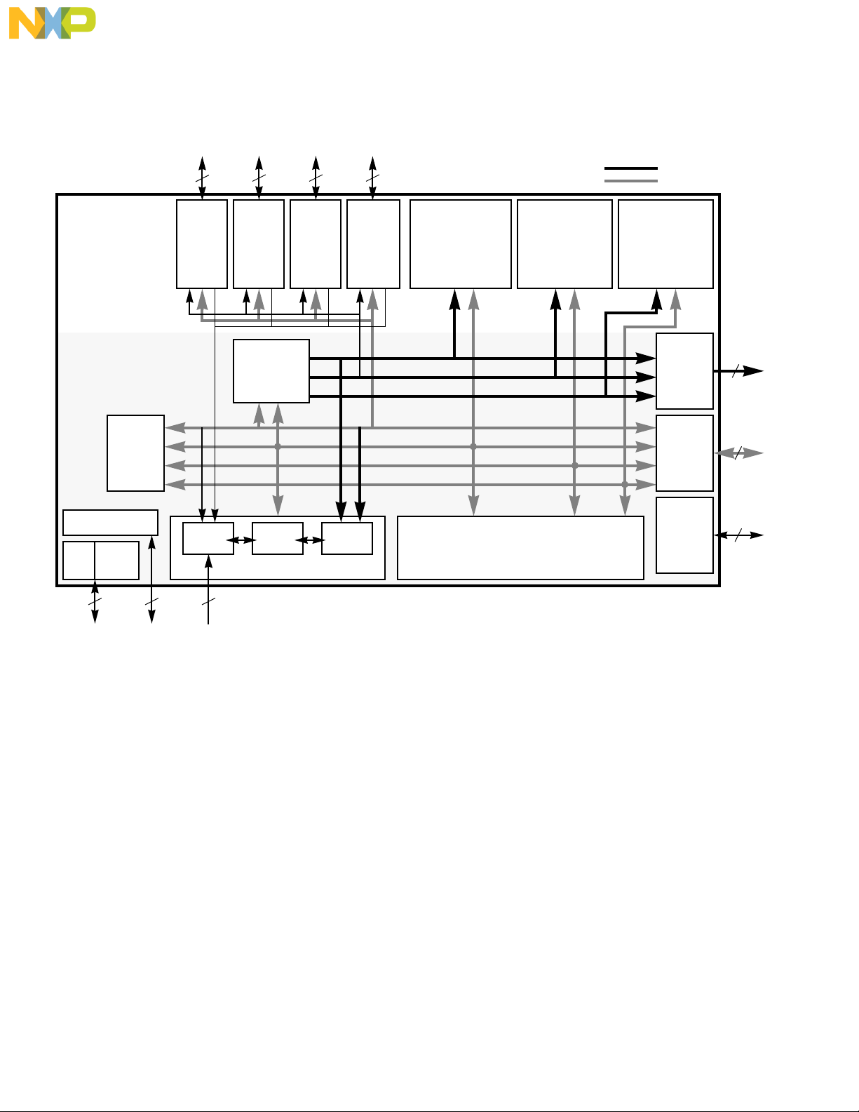
Figure 1-2 DSP56002 Block Diagram
X Data
Memory
256 × 24 RAM
256 × 24 ROM
16-bit Bus
24-bit Bus
Y Data
Memory
256 × 24 RAM
256 × 24 ROM
External
Address
Bus
Switch
External
Data
Bus
Switch
Bus
Control
Address
16
Data
24
Control
10
Frees
DSP56002 User’s Manual Addendum
For More Information On This Product,
Go to: www.freescale.com
MOTOROLA
Page 25

Freescale Semiconductor, Inc.
nc...
I
cale Semiconductor,
Frees
MOTOROLA
For More Information On This Product,
DSP56002 User’s Manual Addendum
Go to: www.freescale.com
3
Page 26
4
Freescale Semiconductor, Inc.
nc...
I
1 0 Yes 1
1 1 Yes 2
IRQA Mode
IRQB Mode
0
*
0
*
0
1 0 Yes 1
1 1 Yes 2
Host IPL
*
*
0
= Reserved, Program as zero
*
cale Semiconductor,
Frees
IAL2 Trigger IAL1 IAL0 Enabled IPL
0 Level 0 0 No —
0 0 No —
0 1 Yes 0
1 0 Yes 1
1 1 Yes 2
HPL1 HPL0 Enabled IPL
SSL1SSL0
1 Neg. Edge 0 1 Yes 0
IBL2 Trigger IBL1 IBL0 Enabled IPL
0 Level 0 0 No —
1 Neg. Edge 0 1 Yes 0
SCL0 HPL1 HPL0 IBL2 IBL1 IBL0 IAL2 IAL1 IAL0
1514131211109876543210
SCL1
TIL0
TIL1
0
*
0
*
0
*
*
0
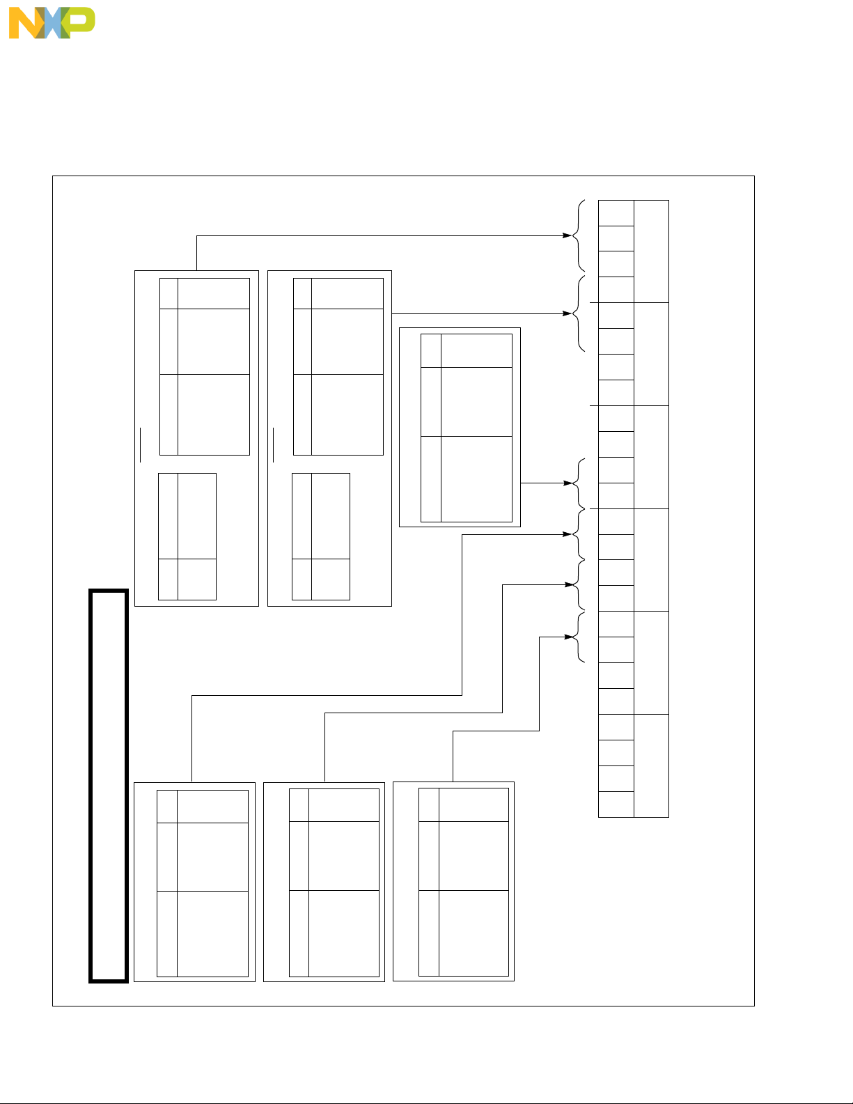
Figure B-4 Interrupt Priority Register (IPR)
$0
0
*
0
*
23 22 21 20 19 18 1617
SSI IPL
SSL1 SSL0 Enabled IPL
0 0 No —
0 1 Yes 0
1 0 Yes 1
SCI IPL
1 1 Yes 2
SCL1 SCL0 Enabled IPL
0 0 No —
0 1 Yes 0
1 0 Yes 1
1 1 Yes 2
TIMER IPL
0 0 No —
TIL1 TIL0 Enabled IPL
0 1 Yes 0
1 0 Yes 1
CENTRAL PROCESSOR
DSP56002 User’s Manual Addendum
For More Information On This Product,
Go to: www.freescale.com
1 1 Yes 2
Register (IPR)
Interrupt Priority
X:$FFFF Read/Write
Reset = $000000
MOTOROLA
Page 27

Freescale Semiconductor, Inc.
nc...
I
cale Semiconductor,
Frees
MOTOROLA
For More Information On This Product,
DSP56002 User’s Manual Addendum
Go to: www.freescale.com
5
Page 28
nc...
I
cale Semiconductor,
Frees
Freescale Semiconductor, Inc.
SSI
Serial Control Direction Bits
0 = Input 1 = Output
Clock Source Direction
0 = External Clock 1 = Internal Clock
Shift Direction
0 = MSB First 1 = LSB First
Frame Sync Length 0
0 = Rx and Tx Same Length 1 = Rx and Tx Different Length
Frame Sync Length 1
0 = Rx is Word Length 1 = Rx is Bit Length
Sync/Async Control
0 = Asynchronous 1 = Synchronous
Gated Clock Control
0 = Continuous Clock 1 = Gated Clock
SSI Mode Select
0 = Normal 1 = Network
Transmit Enable
0 = Disable 1 = Enable
Receive Enable
0 = Disable 1 = Enable
Transmit Interrupt Enable
0 = Disable 1 = Enable
Receive Interrupt Enable
0 = Disable 1 = Enable
SSI
Control Register B (CRB)
X:$FFED Read/Write
Reset = $000000
23
*
0
•••
1514131211109876543210
RIE TIE RE TE MOD GCK SYN FSL1 FSL0SHFDSCKDSCD2SCD1SCD0 OF1 OF0
6
Output Flag x
If SYN = 1 and SCD1=1
OFx SCx Pin
= Reserved, Program as zero
*
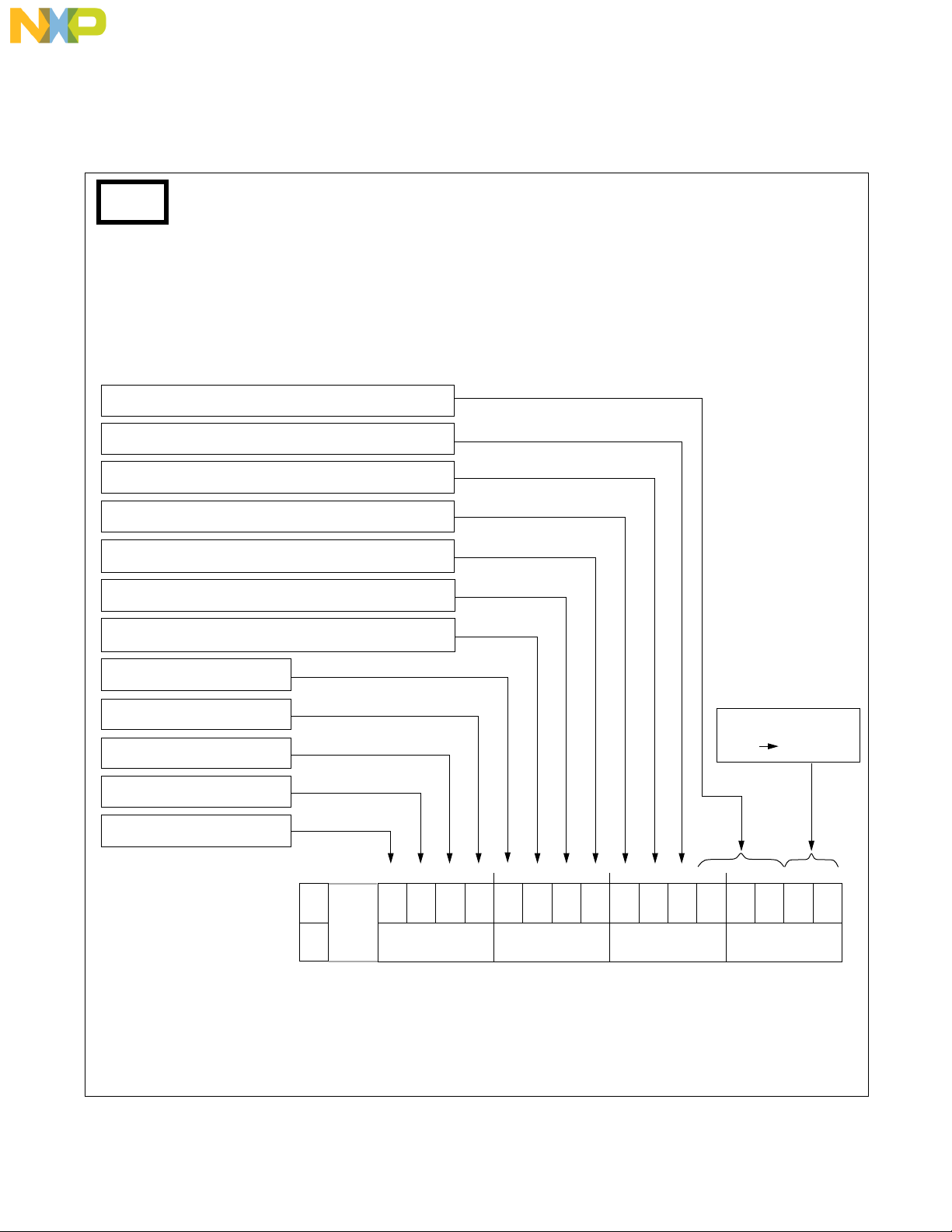
Figure B-32 SSI Control Register B (CRB)
DSP56002 User’s Manual Addendum
For More Information On This Product,
Go to: www.freescale.com
MOTOROLA
Page 29
Freescale Semiconductor, Inc.
TIMER
Timer Control Bits 3-5 (TC0 - TC2)
TC2 TC1 TC0 TIO Clock Mode
0 0 0 GPIO Internal Timer
0 0 1 Output Internal Timer Pulse
0 1 0 Output Internal Timer Toggle
0 1 1 X X Undefined
1 0 0 Input Internal Input Width
1 0 1 Input Internal Input Period
1 1 0 Input External Standard Time Counter
1 1 1 Input External Event Counter
Sheet 1 of 1
Timer Enable Bit 0
0 = Timer Disabled
1 = Timer Enabled
Timer Interrupt Enable Bit 1
0 = Interrupts Disabled
1 = Interrupts Enabled
nc...
I
cale Semiconductor,
Frees
Data Input Bit 9
0 = Zero read on TIO pin
1 = One read on TIO pin
Data Output Bit 10
0 =Zero written to TIO pin
1 = One written to TIO pin
Timer Control and
Status Register (TCSR)
X:$FFDE (Read/Write)
Reset = $000200
Figure B-34 Timer Control and Status Register (TCSR)
GPIO Bit 6
0 = TIO is Timer IO
1 = TIO is GPIO if TC2-TC0 are clear
Timer Status Bit 7
0 = TCSR read, or timer interrupt
serviced
1 = Counter decremented to 0
Direction Bit 8
0 = TIO pin is input
1 = TIO pin is output
23
*
0
•••
1514131211109876543210
*0*0*0*0*
Inverter Bit 2
0 = 0- to-1 transitions on TIO
input decrement the counter
1 = 1-to-0 transitions on TIO
input decrement the counter
Timer pulse inverted before
it goes to TIO output
0
= Reserved, Program as zero
*
or
TETIEINVTC0TC1TC2GPIOTSDIRDIDO
MOTOROLA
For More Information On This Product,
DSP56002 User’s Manual Addendum
Go to: www.freescale.com
7
Page 30

Freescale Semiconductor, Inc.
nc...
I
OnCE is a trademark of Motorola, Inc.
All product and brand names appearing herein are trademarks or registered trademarks of their respective holders.
Motorola reserves the right to make changes without further notice to any products herein. Motorola makes no warranty, representation or guarantee regarding the suitability of its products for any particular purpose, nor does Motorola assume any liability
arising out of the application or use of any product or circuit, and specifically disclaims any and all liability, including without limitation consequential or incidental damages. “Typical” parameters can and do vary in different applications. All operating parameters, including “Typical”, must be validated for each customer application by customer's technical experts. Motorola does not
cale Semiconductor,
convey any license under its patent rights nor the rights of others. Motorola products are not designed, intended, or authorized
for use as components in systems intended for surgical implant into the body, or other applications intended to support or sustain
life, or for any other application in which the failure of the Motorola product could create a situation where personal injury or death
may occur. Should Buyer purchase or use Motorola products for any such unintended or unauthorized application, Buyer shall
indemnify and hold Motorola and its officers, employees, subsidiaries, affiliates, and distributors harmless against all claims,
Frees
costs, damages, and expenses, and reasonable attorney fees arising out of, directly or indirectly, any claim of personal injury or
death associated with such unintended or unauthorized use, even if such claim alleges that Motorola was negligent regarding the
design or manufacture of the part.
Motorola and
Motorola, Inc. is an Equal Opportunity/Affirmative Action Employer.
Literature Distribution Centers:
USA: Motorola Literature Distribution; P.O. Box 20912; Phoenix, Arizona 85036.
EUROPE: Motorola Ltd.; European Literature Centre; 88 Tanners Drive, Blakelands, Milton Keynes, MK14 5BP, United Kingdom.
JAPAN: Nippon Motorola Ltd.; 4-32-1, Nishi-Gotanda, Shinagawa-ku, Tokyo 141 Japan.
ASIA-PACIFIC: Motorola Semiconductors H.K. Ltd.; Silicon Harbor Center, No. 2 Dai King Street, Tai Po Industrial
b are registered trademarks of Motorola, Inc.
Estate, Tai Po, N.T., Hong Kong.
For More Information On This Product,
Go to: www.freescale.com
Page 31

MOTOROLA
SEMICONDUCTOR USER’S MANUAL ADDENDUM
Freescale Semiconductor, Inc.
Order this document by:
DSP56002UMAD2/D
DSP56002
24-BIT DIGITAL SIGNAL PROCESSOR FAMILY
This document, containing changes, additional features, further explanations, and
clarifications, is a second addendum to the original document listed below:
Document Name:
Order Number:
Revision:
Change the following:
Page 5-43 - In the first paragraph after item l0, delete “The code shown in Figure 5-25 is an
excerpt from the Host I/O Port Technical Bulletin (in-house document).” Change the next
nc...
I
cale Semiconductor,
sentence so that it begins “The MAIN PROGRAM in Figure 5-25 initializes...”
Page 7-4 - Change “In Timer Modes 4 and 5” to read “In Timer Modes 4, 5 and 6” in the first
line of the last paragraph.
Page 7-6 - In the second paragraph of section 7.4.4, change “...is given in Chapter 3” to “...is
given in Section 7.5.”
Page 7-20 - In the fifth line of code, change the operand from “#$CF,MR” to #$FC,MR” for
the ANDI instruction.
Page 7-21 - In the eleventh line of code in section 7.8.4, change the operand from “#$CF,MR”
to #$FC,MR” for the ANDI instruction.
Page 7-22 - In the ninth line of code on the page, “#$CF,MR” to #$FC,MR” for the ANDI
instruction.
Page B-3 - In Figure B-1, the Timer Count Register should be shown as 24 bits long instead of
16 bits long.
DSP56002 User’s Manual
DSP56002UM/AD
1
Frees
©1996 MOTOROLA, INC.
For More Information On This Product,
Go to: www.freescale.com
Page 32

nc...
I
Freescale Semiconductor, Inc.
OnCE, Motorola, and are registered trademarks of Motorola, Inc.
Motorola reserves the right to make changes without further notice to any products herein. Motorola makes no
warranty, representation or guarantee regarding the suitability of its products for any particular purpose, nor does
Motorola assume any liability arising out of the application or use of any product or circuit, and specifically
disclaims any and all liability, including without limitation consequential or incidental damages. “Typical”
parameters can and do vary in different applications. All operating parameters, including “Typical”, must be
validated for each customer application by customer’s technical experts. Motorola does not convey any license
under its patent rights nor the rights of others. Motorola products are not designed, intended, or authorized for use
as components in systems intended for surgical implant into the body, or other applications intended to support or
sustain life, or for any other application in which the failure of the Motorola product could create a situation where
personal injury or death may occur. Should Buyer purchase or use Motorola products for any such unintended or
unauthorized application, Buyer shall indemnify and hold Motorola and its officers, employees, subsidiaries,
cale Semiconductor,
affiliates, and distributors harmless against all claims, costs, damages, and expenses, and reasonable attorney
fees arising out of, directly or indirectly, any claim of personal injury or death associated with such unintended or
unauthorized use, even if such claim alleges that Motorola was negligent regarding the design or manufacture of
the part.
Frees
How to reach us:
USA/Europe :
Motorola Literature Distribution
P.O. Box 20912
Phoenix, Arizona 85036
1 (800) 441-2447
Hong Kong :
Motorola Semiconductors H.K. Ltd.
8B Tai Ping Industrial Park
51 Ting Kok Road
Tai Po, N.T., Hong Kong
852-2662928
Japan :
Nippon Motorola Ltd.
Tatsumi-SPD-JLDC
Toshikatsu Otsuki
6F Seibu-Butsuryu-Center
3-14-2 Tatsumi Koto-Ku
Tokyo 135, Japan
03-3521-8315
MFAX :
RMFAX0@email.sps.mot.com
TOUCHTONE (602) 244-6609
Internet :
http://motserv.indirect.com/dsp/DSPhome.html
For More Information On This Product,
Go to: www.freescale.com
Page 33

Freescale Semiconductor, Inc.
SECTION 1
INTRODUCTION TO THE DSP56002
nc...
I
cale Semiconductor,
Frees
MOTOROLA 1 - 1
For More Information On This Product,
Go to: www.freescale.com
Page 34

Freescale Semiconductor, Inc.
1.1 INTRODUCTION . . . . . . . . . . . . . . . . . . . . . . . . . . . . . . . . . . . . . . . . . . . . . 1-3
1.2 FEATURES . . . . . . . . . . . . . . . . . . . . . . . . . . . . . . . . . . . . . . . . . . . . . . . . . 1-4
1.3 DSP56K CENTRAL PROCESSING UNIT OVERVIEW. . . . . . . . . . . . . . . . 1-4
1.4 MANUAL ORGANIZATION . . . . . . . . . . . . . . . . . . . . . . . . . . . . . . . . . . . . . 1-5
nc...
I
SECTION CONTENTS
cale Semiconductor,
Frees
1 - 2 INTRODUCTION TO THE DSP56002 MOTOROLA
For More Information On This Product,
Go to: www.freescale.com
Page 35

Freescale Semiconductor, Inc.
1.1 INTRODUCTION
This manual describes the DSP56002 24-bit digital signal processor, its memory and operating modes, and its peripheral modules. It is intended to be used with the DSP56K
Central Processing Unit Manual (DSP56KFAMUM/AD) , which describes the central processing unit, programming models, and includes details of the instruction set. The
DSP56002 Technical Data Sheet (DSP56002/D) provides timing, pinout, and packaging
descriptions (see Figure 1-1).
This section presents the DSP56002 features.
nc...
I
24-bit
DSP56002
INTRODUCTION
Products
cale Semiconductor,
Frees
DSP56000
Family Manual
# DSP56KFAMUM/AD
DSP56002
User’s Manual
# DSP56002UM/AD
DSP56002
Technical Data
# DSP56002/D
Central Processor and
Instruction Manual
• central processor
• instruction set
Device Manual
• peripherals
• memories
Specification
• electrical
• mechanical
Figure 1-1 DSP56002 Technical Literature
MOTOROLA INTRODUCTION TO THE DSP56002 1 - 3
For More Information On This Product,
Go to: www.freescale.com
Page 36

1.2 FEATURES
DSP56K Central Processing Unit (CPU) Features
• 20 Million Instructions per Second (MIPS) at 40 MHz
• Single-Cycle 24 x 24 Bit Parallel Multiply-Accumulator
• Highly Parallel Instruction Set with Unique DSP Addressing Modes
• Zero Overhead Nested DO Loops
• Fast Auto-Return Interrupts
• Fully Static Logic, Operation Frequency Down to DC
• Very Low-power CMOS Design
• STOP and WAIT Low-power Standby Modes
Freescale Semiconductor, Inc.
FEATURES
nc...
I
cale Semiconductor,
Frees
DSP56002 Features
• 512 x 24 Program RAM
• Two 256 x 24 Data RAM
• Two 256 x 24 Data ROM (Sine and Cosine Tables)
• Full Speed Memory Expansion Port with 16-bit Address and 24-bit Data Buses
• Byte-wide Host Interface with DMA Support
• Synchronous Serial Interface Port
• Serial Communication Interface (Asynchronous) Port
• 24 General Purpose I/O Pins
• 24-bit Timer/Event Counter
*
• On-chip Emulator (OnCE ) for Unobtrusive, Full Speed Debugging
• Optional Program Security Feature Disables Unauthorized Program ROM and
OnCE Access
• PLL Based Clocking with Wide Input Frequency Range, Wide Range Frequency
Multiplication (1 to 4096) and Power Saving Clock Divider (2
i
, i=0,...,15) to
Reduce Clock Noise
1.3 DSP56K CENTRAL PROCESSING UNIT OVERVIEW
The DSP56K series of 24-bit modular processors is built on a common central processing
unit (CPU). In the expansion area around the CPU, the chip can support various configurations of memory and peripheral modules which may change between series members.
* The first version of the DSP56002 (mask number D41G) did not have the timer/event counter. Later versions of the DSP56002 which have
different mask numbers do have the timer/event counter. This mask number can be found below the part number on each chip.
1 - 4 INTRODUCTION TO THE DSP56002 MOTOROLA
For More Information On This Product,
Go to: www.freescale.com
Page 37

Freescale Semiconductor, Inc.
The central components are:
• Data Buses
• Address Buses
• Data Arithmetic Logic Unit (data ALU)
• Address Generation Unit (AGU)
• Program Control Unit (PCU)
• Memory Expansion (Port A)
Figure 1-2 shows a block diagram of the DSP56002, including the CPU and the expansion
area for memory and peripherals. The DSP56000 Family Manual (DSP56KFAMUM/AD)
presents the details of each of the above CPU components.
MANUAL ORGANIZATION
nc...
I
cale Semiconductor,
Frees
1.4 MANUAL ORGANIZATION
This manual includes the following sections:
SECTION 2 — PIN DESCRIPTIONS presents the DSP56002 pinout.
SECTION 3 — MEMORY MODULES AND OPERATING MODES presents the details of
the DSP56002 memory maps and explains the various operating modes that affect the
processor’s program and data memories.
SECTION 4 — PORT A describes the external memory port, its registers, and control
signals.
SECTION 5 — PORT B describes the port B parallel I/O and the host interface, their registers, and their controls.
SECTION 6 — PORT C describes the port C parallel I/O, the Synchronous Serial Interface, the Synchronous Communication Interface, their registers, and their controls.
SECTION 7 — DSP56002 TIMER AND EVENT COUNTER describes the timer/counter
and its registers and controls.
APPENDIX A — BOOTSTRAP PROGRAM
APPENDIX B — PROGRAMMING SHEETS
TROUBLE REPORT — This trouble report is a form that allows the reader to notify the
factory of any errors or discrepancies discovered in this manual.
MOTOROLA INTRODUCTION TO THE DSP56002 1 - 5
For More Information On This Product,
Go to: www.freescale.com
Page 38

Freescale Semiconductor, Inc.
MANUAL ORGANIZATION
3
615
EXPANSION
SCI
INTERFA CE
24-Bit 56K
SSI
INTERFA CE
HOST
INTERFA CE
ADDRESS
GENERATION
UNIT
PROGRAM
512x24 RAM
BOOTSTRAP
64x24 ROM
X MEMORY
RAM
256X24
µ/A ROM
256X24
YAB
XAB
PAB
Y MEMORY
RAM
256X24
SINE ROM
256X24
CPU
nc...
I
YDB
INTERNAL
DATA
BUS
SWITCH
cale Semiconductor,
5
PLL
CLOCK
GENERATOR
PROGRAM
INTERRUPT
CONTROLLER
PROGRAM
DECODE
CONTROLLER
Program Control Unit
PROGRAM
GENERA TOR
ADDRESS
XDB
PDB
GDB
DATA ALU
24X24+56→56-BIT MAC
TWO 56-BIT ACCUMULATORS
AREA
EXTERNAL
ADDRESS
BUS
SWITCH
BUS
CONTROL
EXTERNAL
DATA BUS
SWITCH
OnCE
16
10
24
4
ADDRESS
PORT A
CONTROL
DATA
Frees
2
CLOCK
CONTROL
16 BITS
24 BITS
Figure 1-2 DSP56002 Block Diagram
1 - 6 INTRODUCTION TO THE DSP56002 MOTOROLA
For More Information On This Product,
Go to: www.freescale.com
Page 39

Freescale Semiconductor, Inc.
SECTION 2
DSP56002 PIN DESCRIPTIONS
nc...
I
cale Semiconductor,
Frees
MOTOROLA 2 - 1
For More Information On This Product,
Go to: www.freescale.com
Page 40

Freescale Semiconductor, Inc.
2.1 INTRODUCTION . . . . . . . . . . . . . . . . . . . . . . . . . . . . . . . . . . . . . . . . . . . . . 2-3
2.2 SIGNAL DESCRIPTIONS . . . . . . . . . . . . . . . . . . . . . . . . . . . . . . . . . . . . . . 2-3
2.3 ON-CHIP EMULATION (OnCE) PINS . . . . . . . . . . . . . . . . . . . . . . . . . . . . . 2-11
2.4 PLL PINS . . . . . . . . . . . . . . . . . . . . . . . . . . . . . . . . . . . . . . . . . . . . . . . . . . . 2-14
nc...
I
SECTION CONTENTS
cale Semiconductor,
Frees
2 - 2 DSP56002 PIN DESCRIPTIONS MOTOROLA
For More Information On This Product,
Go to: www.freescale.com
Page 41

Freescale Semiconductor, Inc.
INTRODUCTION
2.1 INTRODUCTION
This section introduces pins associated with the DSP56002. It divides the pins into their
functional groups and explains the role each pin plays in the operation of the chip. It acts
as a reference for following chapters which explain the chip’s peripherals in detail.
2.2 SIGNAL DESCRIPTIONS
The DSP56002 is available in a 132-pin grid array package or surface mount (Plastic Quad
Flat Pack, or PQFP). The input and output signals are organized into the functional groups
indicated in Section Figure 2-1. The signals are discussed in the paragraphs that follow.
nc...
I
cale Semiconductor,
Frees
Functional Group
Number
of Pins
Port A Data Bus 24
Port A Address 19
Port A Bus Control 7
Port B Host Interface 15
Port C Synchronous Comm. Interface 3
Port C Synchronous Serial Interface 6
Interrupt and Mode Control 4
PLL and Clock 7
On-chip Emulation (OnCE) 4
Power (VCC) 16
Ground (GND) 24
Timer 1
Reserved 2
Total (for the PGA package) 132
D0-D23
DGND(6)
DVCC(3)
A0-A15
X/Y
AGND(5)
AVCC(3)
BN
RD
WR
BR
BG
WT
CGND
CVCC
MODC/NMI
MODB/IRQB
MODA/IRQA
RESET
EXTAL
XTAL
QGND(4)
QVCC(4)
RESERVED (2)
DSP56002
Port A
Data
Port A
PS
DS
BS
TIO Timer
Address
Port A
Control
Interrupt/
Mode
Control
132 pins
Port B
HOST
Port C
SCI
Port C
SSI
OnCE
PLL
H0-H7
HA0-HA2
HR/W
HEN
HREQ
HACK
HGND(4)
HVCC(2)
RXD
TXD
SCLK
SVCC
SGND(2)
SC0-SC2
SCK
SRD
STD
DSCK/OS1
DSI/OS0
DSO
DR
PVCC
PGND
PCAP
CKP
PLOCK
PINIT
CLVCC
CLGND
CKOUT
Figure 2-1 DSP56002 Signals
2.2.1 Port A Address and Data Bus
The Port A address and data bus signals control the access to external memory. They are
three-stated during reset unless noted otherwise, and may require pull-up resistors to minimize power consumption and to prevent erroneous operation.
Note: All unused inputs should have pull-up resistors for two reasons: 1) floating inputs
draw excessive power, and 2) a floating input can cause erroneous operation. For
MOTOROLA DSP56002 PIN DESCRIPTIONS 2 - 3
For More Information On This Product,
Go to: www.freescale.com
Page 42

Freescale Semiconductor, Inc.
SIGNAL DESCRIPTIONS
example, during reset, all signals are three-stated. Without pull-up resistors, the BR
and WT signals may become active, causing two or more memory chips to try to
simultaneously drive the external bus, which can damage the memory chips. A pullup resistor in the 50K-ohm range should be sufficient. Also, for future enhancements, all reserved pins (see Section Figure 2-1) should be left unconnected.
2.2.1.1 Address (A0–A15)
These three-state output pins specify the address for external program and data memory
accesses. To minimize power dissipation, A0–A15 do not change state when external
memory spaces are not being accessed.
nc...
I
cale Semiconductor,
Frees
2.2.1.2 Data Bus (D0–D23)
These pins provide the bidirectional data bus for external program and data memory accesses. D0–D23 are in the high-impedance state when the bus grant signal is asserted.
2.2.2 Port A Bus Control
The Port A bus control signals are discussed in the following paragraphs. The bus control
signals provide a means to connect additional bus masters (which may be additional
DSPs, microprocessors, direct memory access (DMA) controllers, etc.) through port A to
the DSP56002. They are three-stated during reset and may require pull-up resistors to
prevent erroneous operation.
2.2.2.1 Program Memory Select (PS
)
This three-state output is asserted only when external program memory is referenced
(see Table 2-1).
Table 2-1 Program and Data Memory Select Encoding
PS DS X/Y External Memory Reference
1 1 1 No Activity
1 0 1 X Data Memory on Data Bus
1 0 0 Y Data Memory on Data Bus
0 1 1 Program Memory on Data Bus (Not Exception)
0 1 0 External Exception Fetch: Vector or Vector +1
0 0 X Reserved
1 1 0 Reserved
2 - 4 DSP56002 PIN DESCRIPTIONS MOTOROLA
For More Information On This Product,
Go to: www.freescale.com
(Development Mode Only)
Page 43

2.2.2.2 Data Memory Select (DS)
This three-state output is asserted only when external data memory is referenced (see Table 2-1).
2.2.2.3 X/Y Select (X/Y)
This three-state output selects which external data memory space (X or Y) is referenced
by DS
(see Table 2-1).
Freescale Semiconductor, Inc.
SIGNAL DESCRIPTIONS
nc...
I
cale Semiconductor,
Frees
2.2.2.4 Read Enable (RD
This three-state output is asserted to read external memory on the data bus (D0–D23).
2.2.2.5 Write Enable (WR)
This three-state output is asserted to write external memory on the data bus (D0–D23).
2.2.2.6 Bus Needed (BN)
The BN
port (Port A). During instruction cycles where the external bus is not required, BN
serted.
has granted the bus (by asserting BG
external accesses are required. If an external access is required and the chip is not the
bus master, it will stop processing and remain in wait states until bus ownership is returned. If the BN
processing has stopped and the DSP is waiting to acquire bus ownership. An external arbiter may use this pin to help decide when to return bus ownership to the DSP.
Note: The BN
During hardware reset, BN is deasserted.
2.2.2.7 Bus Request (BR
When the bus request input (BR
to an external device such as a processor or DMA controller. The external device will become the new master of the external address and data buses while the DSP continues
internal operations using internal memory spaces. When BR
DSP56002 will again assume bus mastership.
output pin is asserted whenever the chip requires the external memory expansion
If an external device has requested the bus by asserting the BR
pin is asserted when the chip is not the bus master, this indicates that
pin cannot be used as an early indication of imminent external bus access
because it is valid later than the other bus control signal BS
)
is deas-
input and the DSP
), the DSP will continue processing as long as no
.
)
) is asserted, the DSP56002 will always relinquish the bus
is deasserted, the
When BR
D23, and the bus control pins (PS
impedance state, after the execution of the current instruction has been completed.
Note: To prevent erroneous operation, the BR
MOTOROLA DSP56002 PIN DESCRIPTIONS 2 - 5
is asserted, the DSP56002 will always release Port A, including A0–A15, D0–
, DS, X/Y, RD, WR, and BS) by placing them in the high-
pin should be pulled up when it is not in use.
For More Information On This Product,
Go to: www.freescale.com
Page 44

Freescale Semiconductor, Inc.
2.2.2.8 Bus Grant (BG)
When this output is asserted, it signals to the external device that it has been granted the external bus (i.e. Port A has been three-stated).This output is deasserted during hardware reset.
SIGNAL DESCRIPTIONS
nc...
I
cale Semiconductor,
Frees
2.2.2.9 Bus Strobe (BS
The BS
of the state of the external bus access by the DSP56002. It may also be used with the bus
wait input, WT
necting asynchronous devices to the DSP, allowing devices with differing timing
requirements to reside in the same memory space, allowing a bus arbiter to provide a fast
multiprocessor bus access, and providing an alternative to the WAIT and STOP instructions to halt the DSP at a known program location and have a fast restart. This output is
deasserted during hardware reset.
2.2.2.10 Bus Wait (WT
For as long as it is asserted by an external device, this input allows that device to force
the DSP56002 to generate wait states. If WT
will be inserted into the current cycle (see the DSP56002 Technical Data Sheet
(DSP56002/D) for timing details.
2.2.3 Interrupt and Mode Control
The interrupt and mode control pins select the chip’s operating mode as it comes out of
hardware reset, and they receive interrupt requests from external sources.
2.2.3.1 Mode Select A/External Interrupt Request A (MODA/IRQA
This input pin has three functions. It works with the MODB and MODC pins to select the
chip’s operating mode, it receives an interrupt request from an external source, and it
turns on the internal clock generator, causing the chip to recover from the stop processing
state. Reset causes this input to act as MODA.
During reset, this pin should be forced to the desired state, because as the chip comes
out of reset, it reads the states of MODA, MODB, and MODC and writes the information
to the Operating Mode Register to set the chip’s operating mode. (Operating Modes are
discussed in SECTION 3 MEMORY MODULES AND OPERATING MODES .) After the
chip has left the reset state, the MODA pin automatically changes to external interrupt
request IRQA
output is asserted when the DSP accesses Port A. It acts as an early indication
, to generate wait states, a feature which provides capabilities such as con-
.
)
)
is asserted when BS is asserted, wait states
)/STOP Recovery
IRQA receives external interrupt requests. It can be programmed to be level sensitive or
negative edge triggered. When the signal is edge triggered, triggering occurs at a voltage
level and is not directly related to the fall time of the interrupt signal. However, as the fall
2 - 6 DSP56002 PIN DESCRIPTIONS MOTOROLA
For More Information On This Product,
Go to: www.freescale.com
Page 45

Freescale Semiconductor, Inc.
time of the interrupt signal increases, the probability that noise on IRQA will generate multiple interrupts also increases.
2.2.3.2 Mode Select B/External Interrupt Request B (MODB/IRQB)
This input pin works with the MODA and MODC pins to select the chip’s operating mode,
and it receives an interrupt request from an external source. Reset causes this input to act
as MODB.
During reset, this pin should be forced to the desired state, because as the chip comes
out of reset, it reads the states of the mode pins and writes the information to the Operating Mode Register, which sets the chip’s operating mode. After the chip has left the reset
state, the MODB pin automatically changes to external interrupt request IRQB
SIGNAL DESCRIPTIONS
.
nc...
I
cale Semiconductor,
Frees
IRQB receives external interrupt requests. It can be programmed to be level sensitive or
negative edge triggered. When the signal is edge triggered, triggering occurs at a voltage
level and is not directly related to the fall time of the interrupt signal. However, as the fall
time of the interrupt signal increases, the probability that noise on IRQB
tiple interrupts also increases.
2.2.3.3 Mode Select C/Non-Maskable Interrupt Request (MODC/NMI)
This input pin works with the MODA and MODB pins to select the chip’s operating mode,
and it receives an interrupt request from an external source. Reset causes this input to act
as MODC.
During reset, this pin should be forced to the desired state, because as the chip comes out
of reset, it reads the states of the mode pins and writes the information to the Operating
Mode Register, which sets the chip’s operating mode. After the chip has left the reset state,
the MODC pin automatically changes to a nonmaskable interrupt request (NMI
The negative-edge triggered NMI receives nonmaskable interrupt requests. Triggering
occurs at a voltage level and is not directly related to the fall time of the interrupt signal.
However, as the fall time of the interrupt signal increases, the probability that noise on NMI
will generate multiple interrupts also increases.
will generate mul-
) input.
2.2.3.4 Reset (RESET
This Schmitt trigger input pin is used to reset the DSP56002. When RESET
the DSP56002 is initialized and placed in the reset state. When RESET
the chip writes the mode pin (MODA, MODB, MODC) information to the operating mode
MOTOROLA DSP56002 PIN DESCRIPTIONS 2 - 7
)
is asserted,
is deasserted,
For More Information On This Product,
Go to: www.freescale.com
Page 46

nc...
I
cale Semiconductor,
Frees
Freescale Semiconductor, Inc.
register, setting the chip’s operating mode. The chip also samples the PINIT pin and
writes its information into the PEN bit of the PLL Control Register, and it samples the CKP
pin to determine the polarity of the CKOUT signal. When the chip comes out of the reset
state, deassertion occurs at a voltage level and is not directly related to the rise time of
the RESET
resets increases with increasing rise time of the RESET
2.2.4 Power and Clock
The power and clock signals are presented in the following paragraphs.
2.2.4.1 Power (Vcc), Ground (GND)
There are six sets of power and ground pins: a set of eight (four power, four ground) for
internal logic; a set of eight (three power, five ground) for the address bus output buffer;
a set of nine (three power, six ground) for the data bus output buffer; a set of eleven (four
power, seven ground) for ports B and C and for the OnCE; a set of one power and one
ground for the PLL; and a set of one power and one ground for the CKOUT pin. Refer to
the pin assignments in the Layout Practices section of the DSP56002 Technical Data
Sheet (DSP56002/D).
2.2.4.2 External Clock/Crystal Input (EXTAL)
The EXTAL input interfaces the internal crystal oscillator input to an external crystal or an
external clock.
2.2.4.3 Crystal Output (XTAL)
This output connects the internal crystal oscillator output to an external crystal. If an external clock is used, XTAL should not be connected. It may be disabled through software
control using the XTLD bit in the PLL control register.
2.2.5 Host Interface
The following paragraphs discuss the host interface signals, which provide a convenient
connection to another processor through Port B on the DSP56002.
signal. However, the probability that noise on RESET will generate multiple
SIGNAL DESCRIPTIONS
signal.
2.2.5.1 Host Data Bus (H0–H7)
This bidirectional data bus transfers data between the host processor and the DSP56002.
It acts as an input unless HEN
puts and allowing the host processor to read DSP56002 data. It is high impedance when
HEN
is deasserted. H0–H7 can be programmed as general-purpose I/O pins (PB0–PB7)
2 - 8 DSP56002 PIN DESCRIPTIONS MOTOROLA
is asserted and HR/W is high, making H0–H7 become out-
For More Information On This Product,
Go to: www.freescale.com
Page 47

Freescale Semiconductor, Inc.
when the host interface is not being used. These pins are configured as GPIO input pins
during hardware reset.
2.2.5.2 Host Address (HA0–HA2)
These inputs provide the address selection for each host interface register. HA0–HA2 can
be programmed as general-purpose I/O pins (PB8–PB10) when the host interface is not
being used. These pins are configured as GPIO input pins during hardware reset.
SIGNAL DESCRIPTIONS
nc...
I
cale Semiconductor,
Frees
2.2.5.3 Host Read/Write (HR/W
This input selects the direction of data transfer for each host processor access. If HR/W
is high and HEN is asserted, H0-H7 are outputs and DSP data is transferred to the host
processor. If HR/W
ferred to the DSP. HR/W
general-purpose I/O pin (PB11) when the host interface is not being used, and is configured as a GPIO input pin during hardware reset.
2.2.5.4 Host Enable (HEN
This input enables a data transfer on the host data bus. When HEN
is high, H0–H7 become outputs and the host processor may read DSP56002 data. When
HEN
is asserted and HR/W is low, H0–H7 become inputs. When HEN is deasserted, host
data is latched inside the DSP. Normally, a chip select signal derived from host address
decoding and an enable clock are used to generate HEN
general-purpose I/O pin (PB12) when the host interface is not being used, and is configured as a GPIO input pin during hardware reset.
2.2.5.5 Host Request (HREQ
This open-drain output signal is used by the host interface to request service from the
host processor, DMA controller, or a simple external controller. HREQ
grammed as a general-purpose I/O (not open-drain) pin (PB13) when the host
interface is not being used.
is low and HEN is asserted, H0-H7 are inputs and host data is trans-
is stable when HEN is asserted. It can be programmed as a
)
)
is asserted and HR/W
. HEN can be programmed as a
)
can be pro-
2.2.5.6 Host Acknowledge (HACK
This input has two functions. It provides a host acknowledge handshake signal for DMA
transfers and it receives a host interrupt acknowledge compatible with MC68000 Family
processors. When the port is defined as the host interface and neither of the HACK pin’s
two functions are being used, the user may program this input as a general-purpose I/O pin.
For more details about the programming options for this pin, see Section 5.3.4.6 Host Ac-
knowledge (HACK
Note: HACK should always be pulled high when it is not in use.
MOTOROLA DSP56002 PIN DESCRIPTIONS 2 - 9
) . This pin is configured as a GPIO input pin during hardware reset.
For More Information On This Product,
Go to: www.freescale.com
)
Page 48

Freescale Semiconductor, Inc.
2.2.6 Serial Communication Interface (SCI)
The following signals relate to the SCI. They are introduced briefly here and described in
more detail in SECTION 6 - PORT C .
2.2.6.1 Receive Data (RXD)
This input receives byte-oriented data and transfers the data to the SCI receive shift register. Input data is sampled on the positive or the negative edge of the receive clock,
depending on how the SCI control register is programmed. RXD can be programmed as
a general-purpose I/O pin (PC0) when it is not being used as an SCI pin, and it is configured as a GPIO input pin during hardware reset.
SIGNAL DESCRIPTIONS
nc...
I
cale Semiconductor,
Frees
2.2.6.2 Transmit Data (TXD)
This output transmits serial data from the SCI transmit shift register. Data changes on the
negative edge of the transmit clock. This output is stable on the positive or the negative
edge of the transmit clock, depending on how the SCI control register is programmed.
TXD can be programmed as a general-purpose I/O pin (PC1) when the SCI TXD function
is not being used, and it is configured as a GPIO input pin during hardware reset.
2.2.6.3 SCI Serial Clock (SCLK)
This bidirectional pin provides an input or output clock from which the transmit and/or receive baud rate is derived in the asynchronous mode, and from which data is transferred
in the synchronous mode. SCLK can be programmed as a general-purpose I/O pin (PC2)
when the SCI SCLK function is not being used, and it is configured as a GPIO input pin
during hardware reset.
2.2.7 Synchronous Serial Interface (SSI)
The SSI signals are presented in the following paragraphs.The SSI operating mode affects the definition and function of SSI control pins SC0, SC1, and SC2. They are
introduced briefly here and are described in more detail in SECTION 6 - PORT C .
2.2.7.1 Serial Clock Zero (SC0)
This bidirectional pin’s function is determined by whether the SCLK is in synchronous or
asynchronous mode. In synchronous mode, this pin is used for serial flag I/O. In asynchronous mode, this pin receives clock I/O. SC0 can be programmed as a general-purpose
I/O pin (PC3) when the SSI SC0 function is not being used, and it is configured as a GPIO
input pin during hardware reset.
2 - 10 DSP56002 PIN DESCRIPTIONS MOTOROLA
For More Information On This Product,
Go to: www.freescale.com
Page 49

Freescale Semiconductor, Inc.
2.2.7.2 Serial Control One (SC1)
The SSI uses this bidirectional pin to control flag or frame synchronization. This pin’s function is determined by whether the SCLK is in synchronous or asynchronous mode.In
asynchronous mode, this pin is frame sync I/O. For synchronous mode with continuous
clock, this pin is serial flag SC1 and operates like the SC0. SC0 and SC1 are independent
serial I/O flags but may be used together for multiple serial device selection. SC1 can be
programmed as a general-purpose I/O pin (PC4) when the SSI SC1 function is not being
used, and it is configured as a GPIO input pin during hardware reset.
2.2.7.3 Serial Control Two (SC2)
The SSI uses this bidirectional pin to control frame synchronization only. As with SC0 and
nc...
I
SC1, its function is defined by the SSI operating mode. SC2 can be programmed as a
general-purpose I/O pin (PC5) when the SSI SC2 function is not being used, and it is configured as a GPIO input pin during hardware reset.
ON-CHIP EMULATION (OnCE) PINS
cale Semiconductor,
Frees
2.2.7.4 SSI Serial Clock (SCK)
This bidirectional pin provides the serial bit rate clock for the SSI when only one clock is
being used. SCK can be programmed as a general-purpose I/O pin (PC6) when it is not
needed as an SSI pin, and it is configured as a GPIO input pin during hardware reset.
2.2.7.5 SSI Receive Data (SRD)
This input pin receives serial data into the SSI receive shift register. SRD can be programmed as a general-purpose I/O pin (PC7) when it is not needed as an SSI pin, and it
is configured as a GPIO input pin during hardware reset.
2.2.7.6 SSI Transmit Data (STD)
This output pin transmits serial data from the SSI transmit shift register. STD can be programmed as a general-purpose I/O pin (PC8) when it is not needed as an SSI pin, and it
is configured as a GPIO input pin during hardware reset.
2.3 ON-CHIP EMULATION (OnCE) PINS
The following paragraphs describe the OnCE pins associated with the OnCE controller
and its serial interface.
2.3.1 Debug Serial Input/Chip Status 0 (DSI/OS0)
Serial data or commands are provided to the OnCE controller through the DSI/OS0 pin
when it is an input. The data received on the DSI pin will be recognized only when the
DSP56K has entered the debug mode of operation. Data is latched on the falling edge of
MOTOROLA DSP56002 PIN DESCRIPTIONS 2 - 11
For More Information On This Product,
Go to: www.freescale.com
Page 50

Freescale Semiconductor, Inc.
the DSCK serial clock. Data is always shifted into the OnCE serial port most significant bit
(MSB) first. When the DSI/OS0 pin is an output, it works in conjunction with the OS1 pin
to provide chip status information (see Section 10 ON CHIP EMULATION (OnCE) in the
DSP56000 Family Manual ). The DSI/OS0 pin is an output when the processor is not in
debug mode. When switching from output to input, the pin is three-stated. During hardware reset, this pin is defined as an output and it is driven low.
Note: To avoid possible glitches, an external pull-down resistor should be attached to this pin.
2.3.2 Debug Serial Clock/Chip Status 1 (DSCK/OS1)
The DSCK/OS1 pin supplies the serial clock to the OnCE when it is an input. The serial
clock provides pulses required to shift data into and out of the OnCE serial port. (Data is
nc...
I
clocked into the OnCE on the falling edge and is clocked out of the OnCE serial port on
the rising edge.) The debug serial clock frequency must be no greater than 1/8 of the processor clock frequency.
ON-CHIP EMULATION (OnCE) PINS
cale Semiconductor,
Frees
The pin is three-stated when it is changing from input to output. When it is an output, it works
with the OS0 pin to provide information about the chip status (see SECTION 10 ON CHIP
EMULATION (OnCE) in the DSP56000 Family Manual ). It is an output when the chip is not
in debug mode. During hardware reset, this pin is defined as an output and is driven low.
Note: To avoid possible glitches, an external pull-down resistor should be attached to this pin.
2.3.3 Debug Serial Output (DSO)
The DSP reads serial data from the OnCE through the DSO output pin, as specified by
the last command received from the external command controller. Data is always shifted
out the OnCE serial port most significant bit (MSB) first. Data is clocked out of the OnCE
serial port on the rising edge of DSCK.
The DSO pin also provides acknowledge pulses to the external command controller.
When the chip enters the debug mode, the DSO pin will be pulsed low to indicate (acknowledge) that the OnCE is waiting for commands. After receiving a read command,
the DSO pin will be pulsed low to indicate that the requested data is available and the
OnCE serial port is ready to receive clocks in order to deliver the data. After receiving
a write command, the DSO pin will be pulsed low to indicate that the OnCE serial port
is ready to receive the data to be written; after the data is written, another acknowledge pulse will be provided.
During hardware reset and when the processor is idle, the DSO pin is held high.
2 - 12 DSP56002 PIN DESCRIPTIONS MOTOROLA
For More Information On This Product,
Go to: www.freescale.com
Page 51

Freescale Semiconductor, Inc.
2.3.4 Debug Request Input (DR)
The debug request input (DR
the external command controller. When DR
current instruction being executed, save the instruction pipeline information, enter the debug mode, and wait for commands to be entered from the DSI line. While in debug mode,
the DR
receiving an acknowledge. It may be necessary to reset the OnCE controller in cases
where synchronization between the OnCE controller and external circuitry is lost. Asserting DR
acknowledge pulse in the DSP is produced, sends the DSP into the debug mode. After
receiving the acknowledge, DR
nc...
I
mand. For more information, see Section 10.6 METHODS OF ENTERING THE DEBUG
MODE in the DSP56000 Family Manual (DSP56KFAMUM/AD).
pin lets the user reset the OnCE controller by asserting it and deasserting it after
when the DSP is in the WAIT or the STOP state, and keeping it asserted until an
PLL PINS
) allows the user to enter the debug mode of operation from
is asserted, it causes the DSP to finish the
must be deasserted before sending the first OnCE com-
cale Semiconductor,
Frees
2.4 PLL PINS
The following pins are dedicated to the PLL operation:
•
Analog PLL Circuit Power (PVCC) — The Vcc input is dedicated to the analog
PLL circuits. The voltage should be well regulated and the pin should be provided with an extremely low impedance path to the Vcc power rail. PVcc should
be bypassed to PGND by a 0.1
chip package.
• Analog PLL Circuit Ground (PGND) — This GND input is dedicated to the an-
alog PLL circuits. The pin should be provided with an extremely low impedance
path to ground. PVcc should be bypassed to PGND by a 0.1
ed as close as possible to the chip package.
• CKOUT Power (CLVCC) — This input acts as VCC for the CKOUT output. The
voltage should be well regulated and the pin should be provided with an extremely low impedance path to the VCC power rail. CLVCC should be bypassed to CLGND by a 0.1
package.
• CKOUT Ground (CLGND) — This input acts as GND for the CKOUT output.
The pin should be provided with an extremely low impedance path to ground.
CLVCC should be bypassed to CLGND by a 0.1
as possible to the chip package.
• PLL Filter Capacitor (PCAP) — This input is used to connect an external capacitor needed for the PLL filter. One terminal of the capacitor is connected to
PCAP while the other terminal is connected to PVCC. The capacitor value is
specified in the DSP56002 Technical Data Sheet (DSP56002/D).
µF capacitor located as close as possible to the
µF capacitor located as close as possible to the chip
µF capacitor locat-
µF capacitor located as close
MOTOROLA DSP56002 PIN DESCRIPTIONS 2 - 13
For More Information On This Product,
Go to: www.freescale.com
Page 52

nc...
I
cale Semiconductor,
Frees
Freescale Semiconductor, Inc.
• Output Clock (CKOUT) — This output pin provides a 50% duty cycle output
clock synchronized to the internal processor clock when the PLL is enabled and
locked. When the PLL is disabled, the output clock at CKOUT is derived from,
and has the same frequency and duty cycle as, EXTAL.
Note: If the PLL is enabled and the multiplication factor is less than or equal to
4, then CKOUT is synchronized to EXTAL. (For information on the
DSP56002’s PLL multiplication factor, see Section Section 3.6 PLL
MULTIPLICATION FACTOR.
• CKOUT Polarity Control (CKP) — This input pin defines the polarity of the CK-
OUT clock output. Strapping CKP through a resistor to GND will make the CKOUT polarity the same as the EXTAL polarity. Strapping CKP through a resistor
to Vcc will make the CKOUT polarity the inverse of the EXTAL polarity. The CKOUT clock polarity is internally latched at the end of the hardware reset, so that
any changes of the CKP pin logic state after deassertion of hardware reset will
not affect the CKOUT clock polarity.
• PLL Initialization Input (PINIT) — During the assertion of hardware reset, the
value at the PINIT input pin is written into the PEN bit of the PLL control register.
The PEN bit enables the PLL by causing it to derive the internal clocks from the
PLL VCO output. When the bit is clear, the PLL is disabled and the chip’s internal clocks are derived from the clock connected to the EXTAL pin. After hardware reset is deasserted, the PINIT pin is ignored.
• Phase and Frequency Locked (PLOCK) — The PLOCK output originates
from the Phase Detector. The chip asserts PLOCK when the PLL is enabled
and has locked on the proper phase and frequency of EXTAL. The PLOCK output is deasserted by the chip if the PLL is enabled and has not locked on the
proper phase and frequency. PLOCK is asserted if the PLL is disabled. PLOCK
is a reliable indicator of the PLL lock state only after the chip has exited the
hardware reset state. During hardware reset, the PLOCK state is determined
by PINIT and by the PLL lock condition.
TIMER/EVENT COUNTER MODULE PIN
2.5 TIMER/EVENT COUNTER MODULE PIN
The bidirectional TIO pin is the pin that provides an interface to the timer/event counter module. When the TIO is used as an input, the module functions as an external event counter,
or it measures external pulse width/signal period. When the TIO is used as an output, the
module functions as a timer and the signal on the TIO pin is the timer pulse. When the timer
module is not using the TIO pin, the TIO can act as a general purpose I/O pin.
2 - 14 DSP56002 PIN DESCRIPTIONS MOTOROLA
For More Information On This Product,
Go to: www.freescale.com
Page 53

Freescale Semiconductor, Inc.
SECTION 3
MEMORY MODULES
AND OPERATING MODES
nc...
I
cale Semiconductor,
Frees
MOTOROLA 3 - 1
For More Information On This Product,
Go to: www.freescale.com
Page 54

Freescale Semiconductor, Inc.
3.1 MEMORY MODULES AND OPERATING MODES. . . . . . . . . . . . . . . . . . . 3-3
3.2 DSP56002 DATA AND PROGRAM MEMORY . . . . . . . . . . . . . . . . . . . . . . 3-3
3.3 DSP56002 OPERATING MODE REGISTER (OMR). . . . . . . . . . . . . . . . . . 3-4
3.4 DSP56002 OPERATING MODES . . . . . . . . . . . . . . . . . . . . . . . . . . . . . . . . 3-7
3.5 DSP56002 INTERRUPT PRIORITY REGISTER. . . . . . . . . . . . . . . . . . . . . 3-12
3.6 DSP56002 PHASE-LOCKED LOOP (PLL) MULTIPLICATION FACTOR. . 3-13
nc...
I
SECTION CONTENTS
cale Semiconductor,
Frees
3 - 2 MEMORY MODULES AND OPERATING MODES MOTOROLA
For More Information On This Product,
Go to: www.freescale.com
Page 55

Freescale Semiconductor, Inc.
MEMORY MODULES AND OPERATING MODES
3.1 MEMORY MODULES AND OPERATING MODES
The memory of the DSP56002 can be partitioned in several ways to provide high-speed
parallel operation and additional off-chip memory expansion. Program and data memory
are separate, and the data memory is, in turn, divided into two separate memory spaces,
X and Y. Both the program and data memories can be expanded off-chip. There are also
two on-chip data read-only memories (ROMs) that can overlay a portion of the X and Y
data memories, and a bootstrap ROM that can overlay part of the program random-access memory (RAM). The data memories are divided into two independent spaces to work
with the two address arithmetic logic units (ALUs) to feed two operands simultaneously to
the data ALU.
The DSP operating modes determine the memory maps for program and data memories
nc...
I
and the start-up procedure when the DSP leaves the reset state. This section describes
the DSP56002 Operating Mode Register (OMR), its operating modes and their associated
memory maps, and discusses how to set and reset operating modes.
cale Semiconductor,
Frees
This section also includes details of the interrupt vectors and priorities and describes the
effect of a hardware reset on the PLL multiplication factor.
3.2 DSP56002 DATA AND PROGRAM MEMORY
The DSP56002 has 512 words of program RAM, 64 words of bootstrap ROM, 256 words
of RAM and 256 words of ROM for each of the X and Y internal data memories. The memory maps are shown in Section Figure 3-1 DSP56002 Memory Maps.
3.2.1 Program Memory
The DSP56002 has 512 words of program RAM and 64 words of factory-programmed
bootstrap ROM.
The bootstrap ROM is programmed to perform the bootstrap operation from the memory
expansion port (port A), from the host interface, or from the SCI. It provides a convenient,
low cost method of loading the program RAM with a user program after power-on reset.
The bootstrap ROM activity is controlled by the MA, MB, and MC bits in the OMR (see 3.3
DSP56002 OPERATING MODE REGISTER (OMR) for a complete explanation of the
OMR and the DSP56002’s operating modes and memory maps).
Addresses are received from the program control logic (usually the program counter) over
the PAB. Program memory may be written using the program memory (MOVEM) instructions. The interrupt vectors are located in the bottom 128 locations ($0000-$007F) of
program memory. Program memory may be expanded to 64K off-chip.
MOTOROLA MEMORY MODULES AND OPERATING MODES 3 - 3
For More Information On This Product,
Go to: www.freescale.com
Page 56

Freescale Semiconductor, Inc.
DSP56002 OPERATING MODE REGISTER (OMR)
3.2.2 X Data Memory
The on-chip X data RAM is a 24-bit-wide, static internal memory occupying the lowest 256
locations (0–255) in X memory space. The on-chip X data ROM occupies locations 256–
511 in the X data memory space and is controlled by the DE bit in the OMR. (See the explanation of the DE bit in Section 3.3.2 Data ROM Enable (Bit 2) . Also, see Figure 3-
1.)The on-chip peripheral registers occupy the top 64 locations of the X data memory
($FFC0–$FFFF). The 16-bit addresses are received from the XAB, and 24-bit data transfers to the data ALU occur on the XDB. The X memory may be expanded to 64K off-chip.
3.2.3 Y Data Memory
The on-chip Y data RAM is a 24-bit-wide internal static memory occupying the lowest 256
nc...
I
locations (0–255) in the Y memory space. The on-chip Y data ROM occupies locations
256–511 in Y data memory space and is controlled by the DE and YD bits in the OMR.
(See the explanations of the DE and YD bits in Sections Section 3.3.2 Data ROM En-
able (Bit 2) and Section 3.3.3 Internal Y Memory Disable Bit (Bit 3) , respectively. Also,
see Figure 3-1.) The 16-bit addresses are received from the YAB, and 24-bit data transfers to the data ALU occur on the YDB. Y memory may be expanded to 64K off-chip.
cale Semiconductor,
Frees
Note: The off-chip peripheral registers should be mapped into the top 64 locations ($FFC0–
$FFFF) to take advantage of the move peripheral data (MOVEP) instruction.
3.3 DSP56002 OPERATING MODE REGISTER (OMR)
Operating modes determine the memory maps for program and data memories, and the
start-up procedure when the DSP leaves the reset state. The processor samples the MODA, MODB, and MODC pins as it leaves the reset state, establishes the initial operating
mode, and writes the operating mode information to the Operating Mode Register. When
the processor leaves the reset state, the MODA and MODB pins become general-purpose
interrupt pins, IRQA
maskable interrupt pin NMI
The OMR is a 24-bit register (only six bits are defined) that controls the current operating
mode of the processor. It is located in the DSP56002’s Program Control Unit (described
in Section 5 of the DSP56000 Family Manual ). The OMR bits are only affected by processor reset and by the ANDI, ORI, MOVEC, BSET, BCLR, and BCHG instructions, which
directly reference the OMR. The OMR format for the DSP56002 is shown in Figure 3-2
OMR Format.
and IRQB, respectively, and the MODC pin becomes the non-
.
3 - 4 MEMORY MODULES AND OPERATING MODES MOTOROLA
For More Information On This Product,
Go to: www.freescale.com
Page 57

Freescale Semiconductor, Inc.
DSP56002 OPERATING MODE REGISTER (OMR)
nc...
I
cale Semiconductor,
Frees
MODE 0
MC=0 MB=0 MA=0
$FFFF
EXTERNAL
$01FF
INTERNAL
RAM
$003F
INTERRUPTS
RESET
$0
INTERNAL P: RAM
INTERNAL RESET
INTERRUPT MAP
$007F
HOST COMMANDS
$0040
ILLEGAL INSTRUCTION INT.
$003E
TIMER INTERRUPT
$003C
$003A
HOST COMMANDS
$0024
SCI INTERRUPTS
SSI INTERRUPTS
EXTERNAL INTERRUPTS
SWI INTERRUPT
TRACE INTERRUPT
STACK ERROR INTERRUPT
RESET
$0000
$FFFF
PROGRAM
MEMORY
SPACE
$7F
INTERRUPT
VECTORS
$0
OPERATING MODE DETERMINES
PROGRAM MEMORY AND RESET
STARTING ADDRESS
MODE 2
MC=0 MB=1 MA=0
$FFFF
$E000
$01FF
$003F
RESET
EXTERNAL
INTERNAL
RAM
INTERRUPTS
$0
INTERNAL P: RAM
EXTERNAL RESET
$FFFF
$01FF
$003F
PERIPHERAL MAP
$FFFF
INTERRUPT PRIORITY
BUS CONTROL
SCI INTERFACE
SSI INTERFACE
HOST INTERFACE
P ARALLEL I/0 INTERF A CE
TIMER
$FFDE
$FFC0
MODE 3
MC=0 MB=1 MA=1
EXTERNAL
INTERRUPTS
RESET
$0
NO INTERNAL P: RAM
EXTERNAL RESET
ON-CHIP
RESERVED
Figure 3-1 DSP56002 Memory Maps
$FFFF
X DATA
MEMORY
SPACE
$0
DE and YD BITS IN THE OMR DETERMINE
THE X AND Y DATA MEMORY MAPS
DE = 1
YD = 0
$FFFF
ON-CHIP
PERIPHERALS
$FFC0
$FFBF
EXTERNAL
X DATA
MEMORY
$01FF
INTERNAL
X ROM -
+A-LAW/LIN
$017F
INTERNAL
X ROM -
+MU-LAW/LIN
$00FF
INTERNAL
X RAM
$0
DATA ROMS ENABLED
$FFFF
ON-CHIP
PERIPHERALS
$FFC0
$FFBF
EXTERNAL
X DATA
MEMORY
$01FF
INTERNAL
X ROM -
+A-LAW/LIN
$017F
INTERNAL
X ROM -
+MU-LAW/LIN
$00FF
INTERNAL
X RAM
$0
NOTE: Addresses $FFC0–$FFFF in X data memory
are NOT available externally
PERIPHERALS
EXTERNAL
INTERNAL
SINE-WAVE
INTERNAL
DE = 1
YD = 1
PERIPHERALS
EXTERNAL
EXTERNAL
Y DATA
MEMORY
Y ROM
FULL
Y RAM
EXTERNAL
Y DATA
MEMORY
$FFFF
$0
$FFFF
$FFC0
$00FF
$FFFF
$FFC0
$00FF
Y DATA
MEMORY
SPACE
ON-CHIP
PERIPHERALS
EXTERNAL
X DATA
MEMORY
INTERNAL
X RAM
$0
DATA ROMS DISABLED
ON-CHIP
PERIPHERALS
INTERNAL
X RAM
$0
DE = 0
YD = 0
DE = 0
YD = 1
PERIPHERALS
EXTERNAL
PERIPHERALS
EXTERNAL
Y DATA
MEMORY
INTERNAL
Y RAM
EXTERNAL
EXTERNAL
Y DATA
MEMORY
MOTOROLA MEMORY MODULES AND OPERATING MODES 3 - 5
For More Information On This Product,
Go to: www.freescale.com
Page 58
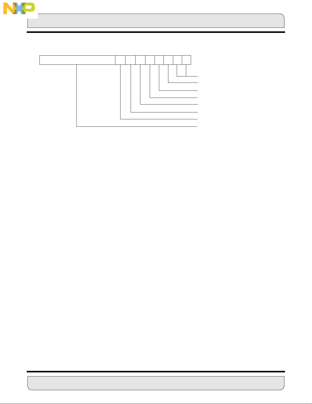
Freescale Semiconductor, Inc.
DSP56002 OPERATING MODE REGISTER (OMR)
23 8 76543210
*
SD MC YD DE MB MA
*
*
OPERATING MODES A, B
DATA ROM ENABLE
INTERNAL Y MEMORY DISABLE
OPERATING MODE C
RESERVED
STOP DELAY
RESERVED
RESERVED
Figure 3-2 OMR Format
nc...
I
3.3.1 Chip Operating Mode (Bits 0 and 1)
The chip operating mode bits, MB and MA, together with MC, define the program memory maps and the operating mode of the DSP56002. On processor reset, MB and MA are
loaded from the external mode select pins, MODB and MODA, respectively. After the
DSP leaves the reset state, MB and MA can be changed under software control.
cale Semiconductor,
Frees
3.3.2 Data ROM Enable (Bit 2)
The DE bit enables the two, on-chip, 256X24 data ROMs located between addresses
$0100–$01FF in the X and Y memory spaces. When DE is cleared, the $0100–$01FF
address space is part of the external X and Y data spaces, and the on-chip data ROMs
are disabled. Hardware reset clears the DE bit.
3.3.3 Internal Y Memory Disable Bit (Bit 3)
Bit 3 is defined as Internal Y Memory Disable (YD). When set, all Y Data Memory addresses are considered to be external, disabling access to internal Y Data Memory. When
cleared, internal Y Data Memory may be accessed according to the state of the DE control
bit. The content of the internal Y Data Memory is not affected by the state of the YD bit.
The YD bit is cleared during hardware reset.
Figure 3-1 DSP56002 Memory Maps shows a graphic representation of the DE and YD
bit effects on the X and Y data memory maps. Table 3-1 also compares the DE and YD
effects on the memory maps.
3 - 6 MEMORY MODULES AND OPERATING MODES MOTOROLA
For More Information On This Product,
Go to: www.freescale.com
Page 59

Freescale Semiconductor, Inc.
DE YD Data Memory
0 0 Internal ROMs Disabled and their addresses are part of
0 1 Internal X Data ROM is Disabled and is part of External
nc...
I
DSP56002 OPERATING MODES
Table 3-1 Memory Mode Bits
External Memory
Memory. Internal Y Data RAM and ROM are Disabled and
are part of External Memory
cale Semiconductor,
Frees
3.3.4 Chip Operating Mode (Bit 4)
The MC bit, together with bits MA and MB, define the program memory map and the operating
mode of the chip. Upon reset, the processor loads this bit from the MODC external mode select pin. After the DSP leaves the reset state, MC can be changed under software control.
3.3.5 Reserved (Bit 5)
This bit is reserved for future expansion and will be read as zero during read operations.
3.3.6 Stop Delay (Bit 6)
The SD bit determines the length of the clock stabilization delay that occurs when the
processor leaves the stop processing state. If the stop delay bit is zero when the chip
leaves the stop state, a 64K clock cycle delay is selected before continuing the stop
instruction cycle. However, if the stop delay bit is one, the delay before continuing the
instruction cycle is long enough to allow a clock stabilization period for the internal clock
to begin oscillating and to stabilize. (See the DSP56002 Technical Data Sheet
(DSP56002/D) for the actual timing values.) When a stable external clock is used, the
shorter delay allows faster start-up of the DSP.
3.3.7 Reserved OMR Bits (Bits 7–23)
These bits are reserved for future expansion and will be read as zero during read operations.
3.4 DSP56002 OPERATING MODES
The user can set the chip operating mode through hardware by pulling high the MODC,
MODB, and MODA pins appropriately, and then assert the RESET pin. When the DSP
leaves the reset state, it samples the mode pins and writes to the OMR to set the initial
operating mode.
MOTOROLA MEMORY MODULES AND OPERATING MODES 3 - 7
For More Information On This Product,
Go to: www.freescale.com
Page 60

Freescale Semiconductor, Inc.
DSP56002 OPERATING MODES
Chip operating modes can also be changed using software to write the operating mode
bits (MC, MB, MA) in the OMR. Changing operating modes does not reset the DSP.
Note: The user should disable interrupts immediately before changing the OMR to pre-
vent an interrupt from going to the wrong memory location. Also, one no-operation
(NOP) instruction should be included after changing the OMR to allow for remapping to occur.
Table 3-2 DSP56002 Operating Mode Summary
nc...
I
cale Semiconductor,
Frees
Operating
Mode
0 0 0 0 Single-Chip Mode - P: RAM enabled, reset @ $0000
1 0 0 1 Bootstrap from EPROM, exit in Mode 0
2 0 1 0 Normal Expanded Mode - P: RAM enabled, reset @ $E000
3 0 1 1 Development Mode - P: RAM disabled, reset @ $0000
4 1 0 0 Reserved for Bootstrap
5 1 0 1 Bootstrap from Host, exit in Mode 0
6 1 1 0 Bootstrap from SCI (external clock), exit in Mode 0
7 1 1 1 Reserved for Bootstrap
MCMBM
A
Description
3.4.1 Single Chip Mode (Mode 0)
In the single-chip mode, all internal program and data RAM memories are enabled (see
Figure 3-1). A hardware reset causes the DSP to jump to internal program memory location $0000 and resume execution. The memory maps for mode 0 and mode 2 (see Figure
3-1) are identical. The difference between the two modes is that reset vectors to program
memory location $0000 in mode 0 and vectors to location $E000 in mode 2.
3.4.2 Bootstrap From EPROM (Mode 1)
The bootstrap modes allow the DSP to load a program from an inexpensive byte-wide
ROM into internal program memory during a power-on reset. On power-up, the waitstate generator adds 15 wait states to all external memory accesses so that slow memory can be used. The bootstrap program uses the bytes in three consecutive memory
locations in the external ROM to build a single word in internal program memory.
3 - 8 MEMORY MODULES AND OPERATING MODES MOTOROLA
For More Information On This Product,
Go to: www.freescale.com
Page 61

Freescale Semiconductor, Inc.
DSP56002 OPERATING MODES
In the bootstrap mode, the chip enables the bootstrap ROM and executes the bootstrap
program. (The bootstrap program code is shown in Appendix A.) The bootstrap ROM contains the bootstrap firmware program that performs initial loading of the DSP56002
program RAM. Written in DSP56002 assembly language, the program initializes the program RAM by loading from an external byte-wide EPROM starting at location P:$C000.
The EPROM is typically connected to the chip’s address and data bus.The data contents
of the EPROM must be organized as shown in Table 3-3 Organization of EPROM Data
Contents.
+5 V
nc...
I
FROM OPEN
COLLECTOR
BUFFER
MBD301
FROM
RESET
FUNCTION
FROM OPEN
cale Semiconductor,
COLLECTOR
BUFFER
*
MBD301
MBD301
DR
DSP56002
BR
HACK
WT
MODA/IRQA
MODC/NMI
*
RESET
*
MODB/IRQB
2716
PS
A0-A10
D0-D7
Notes: 1. *These diodes must be Schottky diodes.
2. All resistors are 15KΩ unless noted otherwise.
3. When in RESET, IRQA
be deasserted by external peripherals.
CE
11
A0-A10
8
D0-D7
, IRQB and NMI must
Frees
ADDRESS OF EXTERNAL
BYTE-WIDE P MEMORY
P:$C000
P:$C001
P:$C002
•
•
•
P:$C5FD
P:$C5FE
P:$C5FF
CONTENTS LOADED
TO INTERNAL P: RAM AT:
P:$0000 LOW BYTE
P:$0000 MID BYTE
P:$0000 HIGH BYTE
•
•
•
P:$01FF LOW BYTE
P:$01FF MID BYTE
P:$01FF HIGH BYTE
Figure 3-3 Port A Bootstrap Circuit
MOTOROLA MEMORY MODULES AND OPERATING MODES 3 - 9
For More Information On This Product,
Go to: www.freescale.com
Page 62

Freescale Semiconductor, Inc.
DSP56002 OPERATING MODES
Table 3-3 Organization of EPROM Data Contents
nc...
I
cale Semiconductor,
Frees
Address of External
Byte-Wide Memory:
P:$C000 P:$0000 low byte
P:$C001 P:$0000 mid byte
P:$C002 P:$0000 high byte
••
••
••
P:$C5FD P:$01FF low byte
P:$C5FE P:$01FF mid byte
P:$C5FF P:$01FF high byte
Contents Loaded to Internal
Program RAM at:
After loading the internal memory, the DSP switches to the single-chip mode (Mode 0) and
begins program execution at on-chip program memory location $0000.
If the user selects Mode 1 through hardware (MODA, MODB, MODC pins), the following
actions occur once the processor comes out of the reset state.
1. The control logic maps the bootstrap ROM into the internal DSP program memory space starting at location $0000.
2. The control logic causes program reads to come from the bootstrap ROM (only
address bits 5–0 are significant) and all writes go to the program RAM (all address bits are significant). This condition allows the bootstrap program to load
the user program from $0000–$01FF.
3. Program execution begins at location $0000 in the bootstrap ROM. The bootstrap ROM program loads program RAM from the external byte-wide EPROM
starting at P:$C000.
4. The bootstrap ROM program ends the bootstrap operation and begins executing
the user program. The processor enters Mode 0 by writing to the OMR. This action is timed to remove the bootstrap ROM from the program memory map and
re-enable read/write access to the program RAM. The change to Mode 0 is
timed to allow the bootstrap program to execute a single-cycle instruction (clear
status register), then a JMP #<00, and begin execution of the user program at
location $0000.
3 - 10 MEMORY MODULES AND OPERATING MODES MOTOROLA
For More Information On This Product,
Go to: www.freescale.com
Page 63

Freescale Semiconductor, Inc.
The user can also get into the bootstrap mode (Mode 1) through software by writing zero
to MC and MB, and one to MA in the OMR. This selection initiates a timed operation to
map the bootstrap ROM into the program address space (after a delay to allow execution
of a single-cycle instruction), and then a JMP #<00 to begin the bootstrap process described previously in steps 1 through 4. This technique allows the user to reboot the
system (with a different program, if desired).
The code to enter the bootstrap mode is as follows:
MOVEP #0,X:$FFFF ;Disable interrupts.
MOVEC #1,OMR ;The bootstrap ROM is mapped
nc...
I
NOP ;Allow one cycle delay for the
DSP56002 OPERATING MODES
;into the lowest 64 locations
;in program memory.
;remapping.
cale Semiconductor,
Frees
JMP <$0 ;Begin bootstrap.
The code disables interrupts before executing the bootstrap code. Otherwise, an interrupt
could cause the DSP to execute the bootstrap code out of sequence because the bootstrap program overlays the interrupt vectors.
3.4.3 Normal Expanded Mode (Mode 2)
In this mode, the internal program RAM is enabled and the hardware reset vectors to location $E000. (The memory maps for Mode 0 and Mode 2 are identical. The difference
for Mode 0 is that, after reset, the instruction at location $E000 is executed instead of the
instruction at $0000 — see Figure 3-1 and Table 3-2).
3.4.4 Development Mode (Mode 3)
In this mode, the internal program RAM is disabled and the hardware reset vectors to location $0000. All references to program memory space are directed to external program
memory. The reset vector points to location $0000. The memory map for this mode is
shown in Figure 3-1 and Table 3-2.
3.4.5 Reserved (Mode 4)
This mode is reserved for future definition. If selected, it defaults to Mode 5.
3.4.6 Bootstrap From Host (Mode 5)
In this mode, the Bootstrap ROM is enabled and the bootstrap program is executed. This is
similar to Mode 1 except that the bootstrap program loads internal P: RAM from the Host Port.
MOTOROLA MEMORY MODULES AND OPERATING MODES 3 - 11
For More Information On This Product,
Go to: www.freescale.com
Page 64

nc...
I
cale Semiconductor,
Frees
Freescale Semiconductor, Inc.
DSP56002 INTERRUPT PRIORITY REGISTER
Note: The difference between Modes 1 and 5 in the DSP56002 and Mode 1 in the
DSP56001 may be considered software incompatibility. A DSP56001 program that
reloads the internal P: RAM from the Host Port by setting MB-MA = 01 (assuming
external pull-up resistor on bit 23 of P:$C000) will not work correctly in the
DSP56002. In the DSP56002, the program would trigger a bootstrap from the external EPROM. The solution is to modify the DSP56001 program to set MC-MA = 101.
3.4.7 Bootstrap From SCI (Mode 6)
In this mode, the Bootstrap ROM is enabled and the bootstrap program is executed. The
internal and/or external program RAM is loaded from the SCI serial interface. The number
of program words to load and the starting address must be specified. The SCI bootstrap
code expects to receive 3 bytes specifying the number of program words, 3 bytes specifying the address from which to start loading the program words, and then 3 bytes for each
program word to be loaded. The number of words, the starting address and the program
words are received least significant byte first, followed by the mid-, and then by the most
significant byte. After receiving the program words, program execution starts at the address where the first instruction was loaded. The SCI is programmed to work in
asynchronous mode with 8 data bits, 1 stop bit, and no parity. The clock source is external
and the clock frequency must be 16x the baud rate. After each byte is received, it is echoed back through the SCI transmitter.
3.4.8 Reserved (Mode 7)
This mode is reserved for future definition. If selected, the processor defaults to Mode 6.
3.5 DSP56002 INTERRUPT PRIORITY REGISTER
Section 7 of the DSP56000 Family Manual describes interrupt (exception) processing in
detail. It discusses interrupt sources, interrupt types, and interrupt priority levels (IPL).
Interrupt priority levels for each on-chip peripheral device and for each external interrupt
source can be programmed under software control by writing to the interrupt priority register. Level 3 interrupts are nonmaskable, and interrupts of levels 0-2 are maskable.
The DSP56002 Interrupt Priority Register (IPR) configuration is shown in Section Figure 3-4 DSP56002 Interrupt Priority Register (IPR). The starting addresses of interrupt
vectors in the DSP56002 are defined as shown in Section Table 3-4 Interrupt Vectors,
while the relative priorities of exceptions within the same IPL are defined as shown in
Section Table 3-5 Exception Priorities Within an IPL).
3 - 12 MEMORY MODULES AND OPERATING MODES MOTOROLA
For More Information On This Product,
Go to: www.freescale.com
Page 65

Freescale Semiconductor, Inc.
DSP56002 PHASE-LOCKED LOOP (PLL) MULTIPLICATION FACTOR
TIL1 TIL0
01110987654321
IAL1 IAL0IAL2IBL0IBL1IBL2HPL0HPL1
IRQA MODE
IRQB MODE
RESERVED
HOST IPL
1223 22 21 20 19 18 17 16 15 14 13
SSL1 SSL0SCL0SCL1
nc...
I
cale Semiconductor,
Frees
SSI IPL
SCI IPL
TIMER IPL
RESERVED
Reserved, read as zero and should be written with zero for future compatibility.
Figure 3-4 DSP56002 Interrupt Priority Register (IPR)
3.6 DSP56002 PHASE-LOCKED LOOP (PLL) MULTIPLICATION FACTOR
Section 9 of the DSP56000 Family Manual discusses the details of the PLL. The multiplication factor determines the frequency at which the Voltage Controlled Oscillator (VCO)
will oscillate. The user sets the multiplication factor by writing to the MF0-MF11 bits in the
PLL control register.
The DSP56002 PLL multiplication factor is set to 1 during hardware reset, which means
that the Multiplication Factor Bits MF0-MF11 in the PLL Control Register (PCTL) are set
to $000.
MOTOROLA MEMORY MODULES AND OPERATING MODES 3 - 13
For More Information On This Product,
Go to: www.freescale.com
Page 66

Freescale Semiconductor, Inc.
DSP56002 PHASE-LOCKED LOOP (PLL) MULTIPLICATION FACTOR
Table 3-4 Interrupt Vectors
nc...
I
cale Semiconductor,
Frees
Interrupt
Starting Address
P:$0000 3 Hardware RESET
P:$0002 3 Stack Error
P:$0004 3 Trace
P:$0006 3 SWI
P:$0008 0 - 2 IRQA
P:$000A 0 - 2 IRQB
P:$000C 0 - 2 SSI Receive Data
P:$000E 0 - 2 SSI Receive Data With Exception Status
P:$0010 0 - 2 SSI Transmit Data
P:$0012 0 - 2 SSI Transmit Data with Exception Status
P:$0014 0 - 2 SCI Receive Data
P:$0016 0 - 2 SCI Receive Data with Exception Status
P:$0018 0 - 2 SCI Transmit Data
P:$001A 0 - 2 SCI Idle Line
P:$001C 0 - 2 SCI Timer
P:$001E 3 NMI
P:$0020 0 - 2 Host Receive Data
P:$0022 0 - 2 Host Transmit Data
P:$0024 0 - 2 Host Command (Default)
P:$0026 0 - 2 Available for Host Command
P:$003A 0 - 2 Available for Host Command
P:$003C 0 - 2 Timer
IPL Interrupt Source
P:$003E 3 Illegal Instruction
P:$0040 0 - 2 Available for Host Command
P:$007E 0 - 2 Available for Host Command
3 - 14 MEMORY MODULES AND OPERATING MODES MOTOROLA
For More Information On This Product,
Go to: www.freescale.com
Page 67

Freescale Semiconductor, Inc.
DSP56002 PHASE-LOCKED LOOP (PLL) MULTIPLICATION FACTOR
Table 3-5 Exception Priorities Within an IPL
Priority Exception
Level 3 (Nonmaskable)
Highest Hardware RESET
Illegal Instruction
NMI
Stack Error
Trace
nc...
I
cale Semiconductor,
Frees
Lowest SWI
Levels 0, 1, 2 (Maskable)
Highest IRQA (External Interrupt)
IRQB (External Interrupt)
Host Command Interrupt
Host Receive Data Interrupt
Host Transmit Data Interrupt
SSI RX Data with Exception Interrupt
SSI RX Data Interrupt
SSI TX Data with Exception Interrupt
SSI TX Data Interrupt
SCI RX Data with Exception Interrupt
SCI RX Data Interrupt
SCI TX Data with Exception Interrupt
SCI TX Data Interrupt
SCI Idle Line Interrupt
SCI Timer Interrupt
Lowest Timer Interrupt
MOTOROLA MEMORY MODULES AND OPERATING MODES 3 - 15
For More Information On This Product,
Go to: www.freescale.com
Page 68

Freescale Semiconductor, Inc.
nc...
I
cale Semiconductor,
Frees
For More Information On This Product,
Go to: www.freescale.com
Page 69

Freescale Semiconductor, Inc.
SECTION 4
PORT A
nc...
I
cale Semiconductor,
Frees
MOTOROLA 4 - 1
For More Information On This Product,
Go to: www.freescale.com
Page 70

Freescale Semiconductor, Inc.
4.1 INTRODUCTION . . . . . . . . . . . . . . . . . . . . . . . . . . . . . . . . . . . . . . . . . . . . . 4-3
4.2 PORT A INTERFACE . . . . . . . . . . . . . . . . . . . . . . . . . . . . . . . . . . . . . . . . . 4-3
4.3 PORT A TIMING . . . . . . . . . . . . . . . . . . . . . . . . . . . . . . . . . . . . . . . . . . . . . 4-9
4.4 PORT A WAIT STATES. . . . . . . . . . . . . . . . . . . . . . . . . . . . . . . . . . . . . . . . 4-13
4.5 BUS CONTROL REGISTER (BCR). . . . . . . . . . . . . . . . . . . . . . . . . . . . . . . 4-13
4.6 BUS STROBE AND WAIT PINS . . . . . . . . . . . . . . . . . . . . . . . . . . . . . . . . . 4-15
4.7 BUS ARBITRATION AND SHARED MEMORY. . . . . . . . . . . . . . . . . . . . . . 4-16
nc...
I
SECTION CONTENTS
cale Semiconductor,
Frees
4 - 2 PORT A MOTOROLA
For More Information On This Product,
Go to: www.freescale.com
Page 71

Freescale Semiconductor, Inc.
4.1 INTRODUCTION
Port A provides a versatile interface to external memory, allowing economical connection
with fast memories/devices, slow memories/devices, and multiple bus master systems.
Port A has two power-reduction features. It can access internal memory spaces, toggling
only the external memory signals that need to change, thereby eliminating unneeded
switching current. Also, if conditions allow the processor to operate at a lower memory
speed, wait states can be added to the external memory access to significantly reduce
power while the processor accesses those memories.
4.2 PORT A INTERFACE
The DSP56002 processor can access one or more of its memory sources (X data mem-
nc...
I
ory, Y data memory, and program memory) while it executes an instruction. The memory
sources may be either internal or external to the DSP. Three address buses (XAB, YAB,
and PAB) and four data buses (XDB, YDB, PDB, and GDB) are available for internal
memory accesses during one instruction cycle. Port A’s one address bus and one data
bus are available for external memory accesses.
INTRODUCTION
cale Semiconductor,
Frees
If all memory sources are internal to the DSP, one or more of the three memory sources
may be accessed in one instruction cycle (i.e., program memory access or program memory access plus an X, Y, XY, or L memory reference). However, when one or more of the
memories are external to the chip, memory references may require additional instruction
cycles because only one external memory access can occur per instruction cycle.
If an instruction cycle requires more than one external access, the processor will make
the accesses in the following priority: X memory, Y memory, and program memory. It
takes one instruction cycle for each external memory access – i.e., one access can be
executed in one instruction cycle, two accesses take two instruction cycles, etc. Since the
external data bus is only 24 bits wide, one XY or long external access will take two instruction cycles. The 16-bit address bus can sustain a rate of one memory access per
instruction cycle (using no-wait-state memory which is discussed in 4.4 PORT A WAIT
STATES ).
Figure 4-1 shows the port A signals divided into their three functional groups: address bus
signals (A0-A15), data bus signals (D0-D15), and bus control. The bus control signals can
be subdivided into three additional groups: read/write control (RD
space selection (including program memory select (PS
X/Y
select) and bus access control (BN, BR, BG, WT, BS).
), data memory select (DS), and
and WR), address
The read/write controls can act as decoded read and write controls, or, as seen in Figure
4-2, Figure 4-3, and Figure 4-4, the write signal can be used as the read/write control, and
the read signal can be used as an output enable (or data enable) control for the memory.
MOTOROLA PORT A 4 - 3
For More Information On This Product,
Go to: www.freescale.com
Page 72

Freescale Semiconductor, Inc.
16 - BIT INTERNAL
ADDRESS BUSES
X ADDRESS (XA)
Y ADDRESS (YA)
PROGRAM ADDRESS (PA)
24 - BIT INTERNAL
nc...
I
DATA BUSES
PORT A INTERFACE
EXTERNAL
ADDRESS BUS
SWITCH
16
EXTERNAL
ADDRESS BUS
A0 - A15
cale Semiconductor,
Frees
X DATA (XD)
Y DATA (YD)
PROGRAM DATA (PD)
GLOBAL DATA (GD)
EXTERNAL
DATA BUS
SWITCH
EXTERNAL
BUS CONTROL
LOGIC
24
EXTERNAL
DATA BUS
D0 - D23
BUS CONTROL SIGNALS
RD –- READ ENABLE
– WRITE ENABLE
WR
– PROGRAM MEMORY SELECT
PS
– DATA MEMORY SELECT
DS
– X MEMORY/Y MEMORY SELECT
X/Y
BN
–- BUS NEEDED
– BUS REQUEST
BR
– BUS GRANT
BG
– BUS WAIT
WT
– BUS STROBE
BS
Figure 4-1 Port A Signals
Decoding in such a way simplifies connection to high-speed random-access memories
4 - 4 PORT A MOTOROLA
For More Information On This Product,
Go to: www.freescale.com
Page 73

Freescale Semiconductor, Inc.
PORT A INTERFACE
nc...
I
cale Semiconductor,
Frees
V
CC
+5 V
ADDRESS BUS
DSP56002
CONTROL
V
GROUND
A0 - A15
DATA BUS
D0 - D23
BUS
SS
RD
WR
PS
DS
X/Y
BN
BR
BG
WT
BS
16
24
ADDRESS
DATA
OE
R/W
CS
PROGRAM MEMORY
24 BIT x N WORDS
Figure 4-2 External Program Space
(RAMs). The program memory select, data memory select, and X/Y select can be considered additional address signals, which extend the directly addressable memory from 64K
words to 192K words total.
Since external logic delay is large relative to RAM timing margins, timing becomes more
difficult as faster DSPs are introduced. The separate read and write strobes used by the
DSP56002 are mutually exclusive, with a guard time between them to avoid an instance
where two data buffers are enabled simultaneously. Other methods using external logic
gates to generate the RAM control inputs require either faster RAM chips or external
data buffers to avoid data bus buffer conflicts.
Figure 4-2 shows an example of external program memory. A typical implementation of
this circuit would use three-byte-wide static memories and would not require any additional logic. The PS
signal is used as the program-memory chip-select signal to enable
the program memory at the appropriate time.
Figure 4-3 shows a similar circuit using the DS
MOTOROLA PORT A 4 - 5
For More Information On This Product,
Go to: www.freescale.com
signal to enable two data memories and
Page 74

Freescale Semiconductor, Inc.
PORT A INTERFACE
nc...
I
cale Semiconductor,
Frees
V
CC
+5 V
ADDRESS BUS
DSP56002
V
GROUND
A0 - A15
DATA BUS
D0 - D23
BUS
CONTROL
SS
RD
WR
PS
DS
X/Y
BN
BR
BG
WT
BS
16
24
DATA DATA ADDRESS ADDRESS
X DATA
MEMORY
24 BITS x N WORDS
OE R/W CS CE OE R/W CS CE
Y DATA
MEMORY
24 BITS x N WORDS
Figure 4-3 External X and Y Data Space
using the X/Y
signal to select between them. The three external memory spaces (program, X data, and Y data) do not have to reside in separate physical memories; a single
memory can be employed by using the PS
, DS, and X/Y signals as additional address
lines to segment the memory into three spaces (see Figure 4-4). Table 4-1 shows how
the PS
, DS, and X/Y signals are decoded.
If the DSP is in the development mode, an exception fetch to any interrupt vector location
will cause the X/Y
signal to go low when PS is asserted. This procedure is useful for
debugging and for allowing external circuitry to track interrupt servicing.
4 - 6 PORT A MOTOROLA
For More Information On This Product,
Go to: www.freescale.com
Page 75

Freescale Semiconductor, Inc.
PORT A INTERFACE
Table 4-1 Program and Data Memory Select Encoding
PS DS X/Y External Memory Reference
1 1 1 No Activity
1 0 1 X Data Memory on Data Bus
1 0 0 Y Data Memory on Data Bus
0 1 1 Program Memory on Data Bus (Not an Exception)
0 1 0 External Exception Fetch: Vector or Vector +1
(Development Mode Only)
0 0 X Reserved
nc...
I
cale Semiconductor,
Frees
1 1 0 Reserved
Figure 4-5 shows a system that uses internal program memory loaded from an external
V
CC
+5 V
ADDRESS BUS
DSP56002
GROUND
A0 - A15
DATA BUS
D0 - D23
BUS
CONTROL
V
SS
RD
WR
PS
DS
X/Y
BN
BR
BG
WT
BS
16
24
A11
U3
U4
A13
A14
A15
U1
U2
A0-A10
CE
OE
R/W
CS
A12
A11
EXTERNAL
PROGRAM
X AND Y MEMORY
$3FFF
4K
PROGRAM
MEMORY
$3000
$2FFF
2K
X DATA
MEMORY
$2800
$27FF
2K
Y DATA
MEMORY
$2000
24 BITS
Figure 4-4 Memory Segmentation
MOTOROLA PORT A 4 - 7
For More Information On This Product,
Go to: www.freescale.com
Page 76

Freescale Semiconductor, Inc.
nc...
I
10
PORT A INTERFACE
D0-D23
2018-55 (3)
A0-A9 A10 CS WE OE
D0-D7
24
8
, IRQB and NMI must
be deasserted by external peripherals.
2. All resistors are 15KΩ unless noted otherwise.
3. When in RESET, IRQA
Notes: 1. *These diodes must be Schottky diodes.
cale Semiconductor,
Frees
+5 V
DS
RD
WR
DSP56002
BR
DR
HACK
WT
11
PS
X/Y
A0-A10
MODA/IRQA
MODC/NMI
*
MBD301
*
MBD301
2716
CE A0-A10
RESET
*
MBD301
D0-D23
MODB/IRQB
Figure 4-5 Port A Bootstrap ROM with X and Y RAM
FROM OPEN
COLLECTOR
BUFFER
FUNCTION
FROM OPEN
COLLECTOR
BUFFER
FROM
RESET
ROM during power-up and splits the data memory space of a single memory bank into X:
4 - 8 PORT A MOTOROLA
For More Information On This Product,
Go to: www.freescale.com
Page 77

Freescale Semiconductor, Inc.
PORT A TIMING
and Y: memory spaces. Although external program memory must be 24 bits, external data
memory does not. Of course, this is application specific. Many systems use 16 or fewer bits
for A/D and D/A conversion and, therefore, they may only need to store 16, 12, or even eight
bits of data. The 24/56 bits of internal precision is usually sufficient for intermediate results.
This is a cost saving feature which can reduce the number of external memory chips.
4.3 PORT A TIMING
The external bus timing is defined by the operation of the address bus, data bus, and bus
control pins. The transfer of data over the external data bus is synchronous with the clock.
The timing A, B, and C relative to the edges of an external clock (see Figure 4-6 and Figure 4-7) are provided in the DSP56002 Advance Information Data Sheet (DSP56002/D) .
nc...
I
This timing is essential for designing synchronous multiprocessor systems. Figure 4-6
shows the port A timing with no wait states (wait-state control is discussed in Section 4.4).
One instruction cycle equals two clock cycles or four clock phases. The clock phases,
which are numbered T0 – T3, are used for timing on the DSP. Figure 4-7 shows the same
timing with two wait states added to the external X: memory access.
cale Semiconductor,
Frees
Four TW clock phases have been added because one wait state adds two T phases and
ONE INSTRUCTION CYCLE
ONE CLOCK CYCLE
INTERNAL CLOCK PHASES
ADDRESS PS, DS, X/Y
RD
READ
CYCLE
DATA IN
WRITE
CYCLE
WR
DATA OUT
T0 T1 T2 T3 T0 T1 T2 T3 T0 T1
A
B
C
Figure 4-6 Port A Bus Operation with No Wait States
MOTOROLA PORT A 4 - 9
For More Information On This Product,
Go to: www.freescale.com
Page 78
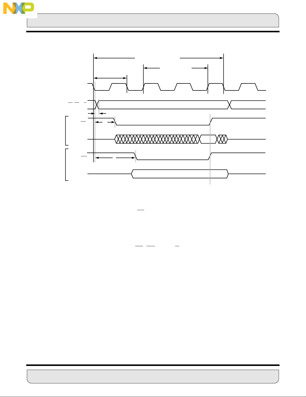
ONE CLOCK CYCLE
INTERNAL CLOCK PHASES
ADDRESS PS, DS, X/Y
Freescale Semiconductor, Inc.
T0 T1 T2 TW TW TW TW T3 T0 T1
A
PORT A TIMING
ONE INSTRUCTION CYCLE
TWO WAIT ST A TES
nc...
I
cale Semiconductor,
Frees
B
C
DATA LATCHED HERE
READ
CYCLE
WRITE
CYCLE
RD
DATA IN
WR
DATA OUT
Figure 4-7 Port A Bus Operation with Two Wait States
is equivalent to repeating the T2 and T2 clock phases. The write signal is also delayed
from the T1 to the T2 state when one or more wait states are added to ease interfacing to
the port. Each external memory access requires the following procedure:
1. The external memory address is defined by the address bus (A0–A15) and the
memory reference selects (PS
, DS, and X/Y). These signals change in the first
phase (T0) of the bus cycle. Since the memory reference select signals have
the same timing as the address bus, they may be used as additional address
lines. The address and memory reference signals are also used to generate
chip-select signals for the appropriate memory chips. These chip-select signals change the memory chips from low-power standby mode to active mode
and begin the read access time. This mode change allows slower memories to
be used since the chip-select signals can be address based rather than read
or write enable based. Read and write enable do not become active until after
the address is valid. See the timing diagrams in the DSP56002 Advance Information Data Sheet (DSP56002/D ) for detailed timing information.
2. When the address and memory reference signals are stable, the data transfer
4 - 10 PORT A MOTOROLA
For More Information On This Product,
Go to: www.freescale.com
Page 79

Freescale Semiconductor, Inc.
is enabled by read enable (RD) or write enable (WR). RD or WR is asserted to
“qualify” the address and memory reference signals as stable and to perform
the read or write data transfer. RD
of the bus cycle (if there are no wait states). Read enable is typically connected to the output enable (OE
output buffers of the chip-selected memory. Write enable is connected to the
write enable (WE
that strobes data into the selected memory. For a read operation, RD
asserted and WR
memory read operation is performed. The DSP data bus becomes an input,
and the memory data bus becomes an output. For a write operation, WR
nc...
I
asserted and RD
the memory chip outputs remain in the high-impedance state even before write
strobe is asserted. This state assures that the DSP and the chip-selected
memory chips are not enabled onto the bus at the same time. The DSP data
bus becomes an output, and the memory data bus becomes an input.
PORT A TIMING
and WR are asserted in the second phase
) of the memory chips and simply controls the
) or write strobe (WS) of the memory chips and is the pulse
is
remains deasserted. Since write enable remains negated, a
is
remains deasserted. Since read enable remains deasserted,
cale Semiconductor,
Frees
3. Wait states are inserted into the bus cycle by a wait-state counter or by asserting WT
value loaded into the wait-state counter is zero, no wait states are inserted into
the bus cycle, and RD
W ≠ 0 is loaded into the wait state counter, W wait states are inserted into the
bus cycle. When wait states are inserted into an external write cycle, WR
delayed from T1 to T2. The timing for the case of two wait states (W=2) is
shown in Figure 4-7.
4. When RD
latched in the destination device – i.e., when RD
latches the data internally; when WR
latches the data on the positive-going edge. The address signals remain stable until the first phase of the next external bus cycle to minimize power dissipation. The memory reference signals (PS
high) during periods of no bus activity, and the data signals are three-stated.
For read-modify-write instructions such as BSET, the address and memory
reference signals remain active for the complete composite (i.e., two I
instruction cycle.
. The wait-state counter is loaded from the bus control register. If the
and WR are asserted as shown in Figure 4-6. If a value
is
or WR are deasserted at the start of T3 in a bus cycle, the data is
is deasserted, the DSP
is deasserted, the external memory
, DS, and X/Y) are deasserted (held
cyc
)
MOTOROLA PORT A 4 - 11
For More Information On This Product,
Go to: www.freescale.com
Page 80

X:$FFFE
Freescale Semiconductor, Inc.
EXTERNAL
X MEMORY
15 12 11 8 7430
0100 1000 1010 1101
PORT A TIMING
PORT A BUS CONTROL REGISTER (BCR)
EXTERNAL
Y MEMORY
EXTERNAL
P MEMORY
EXTERNAL
I/0 MEMORY
D/A
CONVERTER
CS WRDCSRDD
350 ns
(13 WAIT STATES)
nc...
I
A0 - A15
D0 - D23
MEMORY
INTERNAL
(0 WAIT STATES)
cale Semiconductor,
40 MHz
DSP56002
A15
A15
6242 - 15
6242 - 15
6242 - 15 2764 - 25
8K x 24
X RAM
150 ns
(4 WAIT STATES)
CS CS WE OE CS OE CE OE
2764 - 25
2764 - 25
8K x 24
Y ROM
250 ns
(8 WAIT STATES)
27256 - 30
27256 - 30
(10 WAIT STATES)
CONVERTER
27256 - 30
32K x 24
P ROM
300 ns
A/D
Frees
X/Y
DS
WR
RD
PS
Figure 4-8 Mixed-Speed Expanded System
4 - 12 PORT A MOTOROLA
For More Information On This Product,
Go to: www.freescale.com
Page 81

Freescale Semiconductor, Inc.
PORT A WAIT STATES
Figure 4-8 shows an example of mixing different memory speeds and memory-mapped
peripherals in different address spaces. The internal memory uses no wait states, X: memory
uses two wait states, Y: memory uses four wait states, P: memory uses five wait states, and
the analog converters use 14 wait states. Controlling five different devices at five different
speeds requires only one additional logic package. Half the gates in that package are used
to map the analog converters to the top 64 memory locations in Y: memory.
4.4 PORT A WAIT STATES
The DSP56002 features two methods to allow the user to accommodate slow memory
by changing the port A bus timing. The first method uses the bus control register (BCR),
which allows a fixed number of wait states to be inserted in a given memory access to all
locations in each of the four memory spaces: X, Y, P, and I/O. The second method uses
nc...
I
the bus strobe (BS
) and bus wait (WT) facility, which allows an external device to insert
an arbitrary number of wait states when accessing either a single location or multiple
locations of external memory or I/O space. Wait states are executed until the external
device releases the DSP to finish the external memory cycle.
cale Semiconductor,
Frees
Table 4-2 Wait State Control
BCR
Contents
0 Deasserted 0
0 Asserted 2 (minimum)
> 0 Deasserted Equals value in BCR
> 0 Asserted Minimum equals 2 or value in BCR.
WT
Number of Wait States Generated
Maximum is determined by BCR or WT
whichever is larger.
,
4.5 BUS CONTROL REGISTER (BCR)
The BCR determines the expansion bus timing by controlling the timing of the bus interface signals, RD
and WR, and the data output lines. It is a memory mapped register
located at X:$FFFE. Each of the memory spaces in Figure 4-9 (X data, Y data, program
data, and I/O) has its own 4-bit BCR, which can be programmed for inserting up to 15
wait states (each wait state adds one-half instruction cycle to each memory access – i.e.,
50 ns for a 20-Mhz clock). In this way, external bus timing can be tailored to match the
speed requirements of the different memory spaces. On processor reset, the BCR is
preset to all ones (15 wait states). This allows slow memory to be used for boot strap-
ping. The BCR needs to be set appropriately for the memory being used or the processor
will insert 15 wait states between each memory fetch and cause the DSP to run slow.
MOTOROLA PORT A 4 - 13
For More Information On This Product,
Go to: www.freescale.com
Page 82

Freescale Semiconductor, Inc.
15 12 11 8 7430
BUS CONTROL REGISTER (BCR)
nc...
I
cale Semiconductor,
Frees
X:$FFFE
$FFFF
$200
0
* Zero to 15 wait states can be inserted into each external memory access.
EXTERNAL
X MEMORY
EXTERNAL
PROGRAM
MEMORY
INTERNAL
PROGRAM
PROGRAM
MEMORY SPACE
*
RAM
EXTERNAL
Y MEMORY
$FFFF
$FFFE
$FFC0
$200
$100
0
*
BUS CONTROL REGISTER
ON-CHIP PERIPHERALS
EXTERNAL
X DATA
MEMORY
INTERNAL
X ROM
INTERNAL
X RAM
X DATA
MEMORY
SPACE
EXTERNAL
P MEMORY
*
$FFFF
$FFC0
$200
$100
EXTERNAL
I/0 MEMORY
EXTERNAL
PERIPHERALS
EXTERNAL
Y DATA
MEMORY
INTERNAL
Y ROM
INTERNAL
0
Y RAM
Y DATA
MEMORY
SPACE
*
Figure 4-9 Bus Control Register
Figure 4-9 illustrates which of the four BCR subregisters affect which external memory
space. All the internal peripheral devices are memory mapped, and their control registers
reside between X:$FFC0 and X:$FFFF.
To load the BCR the way it is shown in Figure 4-8, execute a “MOVEP #$48AD,
X:$FFFE” instruction. Or, change the individual bits in one of the four subregisters by
using the BSET and BCLR instructions which are detailed in the DSP56000 Family Manual , SECTION 6 and APPENDIX A .
Figure 4-8 shows an example of mixing different memory speeds and memory-mapped
peripherals in different address spaces. The internal memory uses no wait states, X: memory uses two wait states, Y: memory uses four wait states, P: memory uses five wait states,
and the analog converters use 14 wait states. Controlling five different devices at five different speeds requires only one additional logic package. Half the gates in that package
are used to map the analog converters to the top 64 memory locations in Y: memory.
4 - 14 PORT A MOTOROLA
For More Information On This Product,
Go to: www.freescale.com
Page 83

Freescale Semiconductor, Inc.
BUS STROBE AND WAIT PINS
OPERATING MODE REGISTER
765 43210
EM SD 0 0 0 DE MB MA
SET EM = 1
nc...
I
cale Semiconductor,
Frees
V
+5 V
DSP56000/DSP56001
ADDRESS BUS
BUS
CONTROL
CC
GROUND
A0 - A15
DATA BUS
D0 - D23
V
SS
T0 T1 T2 TW TW TW TW T3 T0
16
A0 - A15, D0 - D23, PS, DS, X/Y
24
WT IS
SAMPLED
RD
WR
PS
DS
X/Y
WT
BS
WT IS
SAMPLED
WT IS
SAMPLED
T3
Figure 4-10 Bus Strobe/Wait Sequence
Adding wait states to external memory accesses can substantially reduce power requirements. Consult the DSP56002 Technical Data Sheet (DSP56002/D) for specific power
consumption requirements.
4.6 BUS STROBE AND WAIT PINS
The ability to insert wait states using BS
and WT provides a means to connect asynchronous devices to the DSP, allows devices with differing timing requirements to reside in the
same memory space, allows a bus arbiter to provide a fast multiprocessor bus access, and
provides another means of halting the DSP at a known program location with a fast restart.
The timing of the BS
and WT pins is illustrated in Figure 4-10. Every external access, BS
is asserted concurrently with the address lines in T0. BS can be used by external wait-
MOTOROLA PORT A 4 - 15
For More Information On This Product,
Go to: www.freescale.com
Page 84

Freescale Semiconductor, Inc.
BUS ARBITRATION AND SHARED MEMORY
state logic to establish the start of an external access. BS is deasserted in T3 of each
external bus cycle, signaling that the current bus cycle will complete. Since the WT
is internally synchronized, it can be asserted asynchronously with respect to the system
clock. The WT
BS
is deasserted will give indeterminate results. However, for the number of inserted wait
states to be deterministic, WT
negative-going edge of EXTAL. The setup and hold times are provided in the DSP56002
Advance Information Data Sheet (DSP56002/D) . The timing of WR
BCR and is independent of WT
using the WT
the minimum number of wait states that are inserted. Table 4-2 summarizes the effect of
nc...
I
the BCR and WT
4.7 BUS ARBITRATION AND SHARED MEMORY
The DSP56002 has five pins that control port A. They are bus needed (BN), bus request
(BR
), bus grant (BG), bus strobe (BS) and bus wait (WT) and they are described in SEC-
TION 2 DSP56002 PIN DESCRIPTIONS.
signal should only be asserted while BS is asserted. Asserting WT while
pin is two. The BCR is still operative when using BS and WT and defines
pin on the number of wait states generated.
signal
timing must satisfy setup and hold timing with respect to the
is controlled by the
. The minimum number of wait states that can be inserted
cale Semiconductor,
Frees
The bus control signals provide the means to connect additional bus masters (which may be
additional DSPs, microprocessors, direct memory access (DMA) controllers, etc.) to the port
A bus. They work together to arbitrate and determine what device gets access to the bus.
If an external device has requested the external bus by asserting the BR
DSP has granted the bus by asserting BG
requires no external bus accesses itself. If the DSP does require an external access but
is not the bus master, it will stop processing and remain in wait states until it regains bus
ownership. The BN
help “arbitrate”, or decide when to return bus ownership to the chip.
Four examples of bus arbitration will be described later in this section: 1) bus arbitration
using only BR
external control, 3) bus arbitration using BR
signaling using semaphores.
The BR
while the DSP continues internal operations using internal memory spaces. This allows a
bus controller to arbitrate a multiple bus-master system. (A bus master can issue
addresses on the bus; a bus slave can respond to addresses on the bus. A single device
can be both a master and a slave, but can only be one or the other at any given time.)
input allows an external device to request and be given control of the external bus
pin will have been asserted, and an external device may use BN to
and BG with internal control, 2) bus arbitration using BN, BR, and BG with
, the DSP will continue to process as long as it
, BG and WT, BS with no overhead, and 4)
input, and the
4 - 16 PORT A MOTOROLA
For More Information On This Product,
Go to: www.freescale.com
Page 85

BR
BG
DSP56002
BUS MASTER
A0 - A15, D0 - D23, PS,
, X/Y, RD, WR
DS
Figure 4-11 Bus Request/Bus Grant Sequence
Freescale Semiconductor, Inc.
BUS ARBITRATION AND SHARED MEMORY
A DIFFERENT
BUS MASTER
DSP56002
BUS MASTER
nc...
I
cale Semiconductor,
Frees
Before BR is asserted, all port A signals are driven. When BR is asserted (see Figure 4-11), the
DSP will assert BG
after the current external access cycle completes and will simultaneously
three-state (high-impedance) the port A signals (see the DSP56002 Technical Data Sheet
(DSP56002/D) for exact timing of BR
and BG). The bus is then available to whatever external
device has bus mastership. The external device will return bus mastership to the DSP by deasserting BR
without wait states), BG
and RD
. After the DSP completes the current cycle (an internally executed instruction with or
will be deasserted. When BG is deasserted, the A0-A15, PS, DS, X/Y,
, WR lines will be driven. However, the data lines will remain in three-state. All signals
are now ready for a normal external access.
During the wait state (see Section 7 in the DSP56000 Family Manual), the BR
and BG
circuits remain active. However, the port is inactive - the control signals are deasserted,
the data signals are inputs, and the address signals remain as the last address read or
written. When BR
shows the status of BR
is asserted, all signals are three-stated (high impedance). Table 4-3
and BG during the wait state.
Table 4-3 BR and BG During WAIT
Signal
MOTOROLA PORT A 4 - 17
Before BR
Asserted
For More Information On This Product,
While BG
Asserted
Go to: www.freescale.com
After BR
Deasserted
After Return to
Normal State
(BG Deasserted)
After First
External Access
Page 86

Freescale Semiconductor, Inc.
BUS ARBITRATION AND SHARED MEMORY
4.7.1 Bus Arbitration Using Only BR and BG With Internal Control
Perhaps the simplest example of a shared memory system using a DSP56002 is shown
in Figure 4-12. The bus arbitration is performed within the DSP#2 by using software.
DSP#2 controls all bus operations by using I/O pin OUT2 to three-state its own port A
and by never accessing port A without first calling the subroutine that arbitrates the bus.
When the DSP#2 needs to use external memory, it uses I/O pin OUT1 to request bus
access and I/O pin IN1 to read bus grant. DSP#1 does not need any extra code for bus
arbitration since the BR
protocol for bus arbitration is as follows:
and BG hardware handles its bus arbitration automatically. The
nc...
I
cale Semiconductor,
Frees
At reset: DSP#2 sets OUT2=0 (BR
access to the bus and suspends DSP#2 bus access.
When DSP#2 wants control of the memory, the following steps are performed (see Figure 4-13):
1. DSP# 2 sets OUT1=0 (BR
2. DSP# 2 waits for IN1=0 (BG#1=0 and DSP#1 off the bus).
3. DSP#2 sets OUT2=1 (BR#2=1 to let DSP#2 control the bus).
4. DSP#2 accesses the bus for block transfers, etc. at full speed.
5. To release the bus, DSP#2 sets OUT2=0 (BR#2=0) after the last external
access.
6. DSP#2 then sets OUT1=1 (BR
7. DSP#1 then acknowledges mastership by deasserting BG#1.
4.7.2 Bus Arbitration Using BN
Figure 4-14 can be implemented with external bus arbitration logic, which will save processing capacity on the DSPs and can make bus access much faster at a cost of additional hardware. The bus arbitration logic takes control of the external bus by deasserting
an enable signal (E1, E2, and E3) to all DSPs, which will then acknowledge by granting
the bus (BG
WAIT state with BN
the bus to DSP#1 by asserting E1 (E2 for DSP#2; E3 for DSP#3) to let the DSP know
that it can have the bus. DSP#1 will then deassert BG
trol of the bus. When the DSP no longer needs to make an external access it will deassert BN
=0). When a DSP (DSP#1 in Figure 4-14) needs the bus, it will enter the
asserted. If DSP#1 has highest priority, the arbitration logic grants
and the arbiter deasserts E1, after which the DSP deasserts BG.
#2=0) and OUT1=1 (BR#1=1), which gives DSP#1
#1=0).
#1=1) to return control of the bus to DSP#1.
, BR, and BG With External Control
to tell the arbiter it has taken con-
4 - 18 PORT A MOTOROLA
For More Information On This Product,
Go to: www.freescale.com
Page 87

Freescale Semiconductor, Inc.
BUS ARBITRATION AND SHARED MEMORY
BR
OUT2
BR
BG
CONTROL
A0 - A15
D0 - D23
nc...
I
DSP56002 #1
CAD
MEMORY
BANK
Figure 4-12 Bus Arbitration Using Only BR and BG with Internal Control
cale Semiconductor,
OUT1
OUT1
IN1
CONTROL
A0 - A15
D0 - D23
DSP56002 #2
BUS ARBITER
Frees
IN1
OUT2
1234567
DATA
TRANSFERRED
HERE
Figure 4-13 Two DSPs with External Bus Arbitration Timing
MOTOROLA PORT A 4 - 19
For More Information On This Product,
Go to: www.freescale.com
Page 88
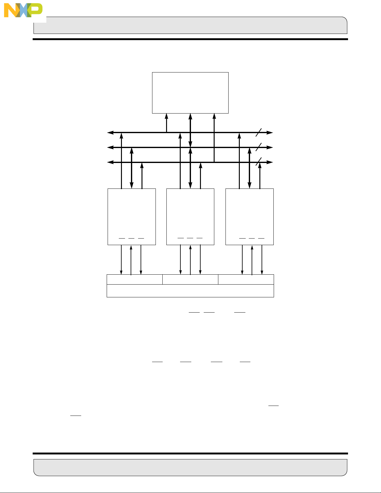
Freescale Semiconductor, Inc.
BUS ARBITRATION AND SHARED MEMORY
SYSTEM MEMORY
32K x 24 X DATA RAM
32K x 24 Y DATA RAM
32K x 24 PROGRAM RAM
ADDRESS DATA CONTROL
ADDRESS
DATA
CONTROL
nc...
I
ADC ADC ADC
DSP56002 #1 DSP56002 #2 DSP56002 #3
BG BR BN
A1 E1 BR1
BUS ARBITRATION LOGIC WITH PRIORITY ENCODER
BG BR BN
A2 E2 BR2
BG BR BN
A3 E3 BR3
cale Semiconductor,
Figure 4-14 Bus Arbitration Using BN, BR, and BG with External Control
16
24
5
Frees
4.7.3 Bus Arbitration Using BR and BG, and WT and BS With No Overhead
By using the circuit shown in Figure 4-15, two DSPs can share memory with hardware
arbitration that requires no software on the part of the DSPs. The protocol for bus arbitration in Figure 4-15 is as follows:
At RESET assume DSP#1 is not making external accesses so that BR
Hence, BG
of DSP#2 is deasserted, which three-states the buffers, giving DSP#2 control
#2 is deasserted.
of the memory.
4 - 20 PORT A MOTOROLA
For More Information On This Product,
Go to: www.freescale.com
Page 89

Freescale Semiconductor, Inc.
BUS ARBITRATION AND SHARED MEMORY
MEMORY
DAC
nc...
I
cale Semiconductor,
Frees
DSP #1
D0 - D23
A0 - A15
RD, WR,
DS, PS, X/Y
BS WT
THREE-STATE
BUFFER
DIR
ENABLE
DSP #2
D0 - 23
A0 - A15
, WR,
RD
DS
, PS, X/Y
BG BR
Figure 4-15 Bus Arbitration Using BR and BG,
and WT
and BS with No Overhead
When DSP#1 wants control of the memory the following steps are performed (see Figure 4-16):
1. DSP#1 makes an external access, thereby asserting BS, which asserts WT
(causing DSP#1 to execute wait states in the current cycle) and asserts
DSP#2 BR
(requesting that DSP#2 release the bus).
2. When DSP#2 finishes its present bus cycle, it three-states its bus drivers and
asserts BG
signals on the memory bus. Asserting BG
. Asserting BG enables the three-state buffers, placing the DSP#1
also deasserts WT, which allows
DSP#1 to finish its bus cycle.
3. When DSP#1’s memory cycle is complete, it releases BS
BR
. DSP#2 then deasserts BG, three-stating the buffers and allowing DSP#2
, which deasserts
to access the memory bus.
MOTOROLA PORT A 4 - 21
For More Information On This Product,
Go to: www.freescale.com
Page 90
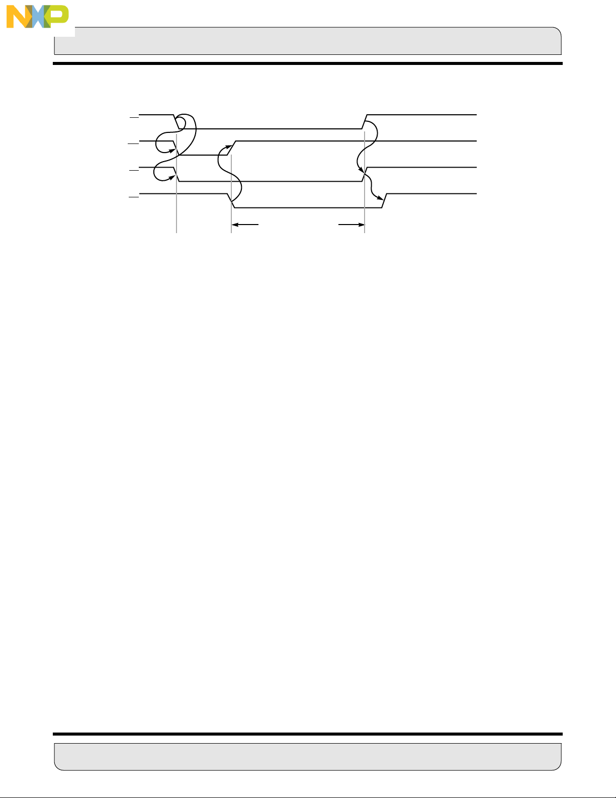
BS
WT
BR
BG
Freescale Semiconductor, Inc.
BUS ARBITRATION AND SHARED MEMORY
12 3
DATA TRANSFERRED
BETWEEN DSP#1
AND MEMORY HERE
nc...
I
cale Semiconductor,
Frees
Figure 4-16 Two DSPs with External Bus Arbitration Timing
4.7.4 Signaling Using Semaphores
Figure 4-17 shows a more sophisticated shared memory system that uses external arbitration with both local external memory and shared memory. The four semaphores are
bits in one of the words in each shared memory bank used by software to arbitrate memory use. Semaphores are commonly used to indicate that the contents of the semaphore’s memory blocks are being used by one processor and are not available for use by
another processor. Typically, if the semaphore is cleared, the block is not allocated to a
processor; if the semaphore is set, the block is allocated to a processor.
Without semaphores, one processor may try to use data while it is being changed by
another processor, which may cause errors. This problem can occur in a shared memory
system when separate test and set instructions are used to “lock” a data block for use by
a single processor.
The correct procedure is to test the semaphore and then set the semaphore if it was
clear to lock and gain exclusive use of the data block. The problem occurs when the second processor acquires the bus and tests the semaphore after the first processor tests
the semaphore but before the first processor can lock the data block. The incorrect
sequence is:
1. the first processor tests the semaphore and sees that the block is available
2. the second processor then tests the bit and also sees that the block is available
3. both processors then set the bit to lock the data
4. both proceed to use the data on the assumption that the data cannot be
changed by another processor
4 - 22 PORT A MOTOROLA
For More Information On This Product,
Go to: www.freescale.com
Page 91

Freescale Semiconductor, Inc.
BUS ARBITRATION AND SHARED MEMORY
DSP56002
LOCAL
MEMORY
nc...
I
SEMAPHORE 3
1
BANK 3
SEMAPHORE 2
0
BANK 2
SEMAPHORE 1
0
BANK 1
SEMAPHORE 0
1
BANK 0
PROCESSOR
LOCAL
MEMORY
cale Semiconductor,
Frees
DSP56002 PROCESSOR
ADDRESS
DATA AND
CONTROL
BUSES
BUS
BUFFER
ARBITRATION
LOGIC
BUS
BUFFER
ADDRESS
DATA AND
CONTROL
BUSES
OR DMA
Figure 4-17 Signaling Using Semaphores
The DSP56K processor series has a group of instructions designed to prevent this problem. They perform an indivisible read-modify-write operation and do not release the bus
between the read and write (specifically, A0–A15, DS
, PS, and X/Y do not change state).
Using a read-modify-write operation allows these instructions to test the semaphore and then to set, clear, or change the semaphore without the possibility of
another processor testing the semaphore before it is changed. The instructions are
bit test and change (BCHG), bit test and clear (BCLR), and bit test and set (BSET).
(They are discussed in detail in the DSP56000 Family Manual.) The proper way to set
the semaphore to gain exclusive access to a memory block is to use BSET to test the
semaphore and to set it to one. After the bit is set, the result of the test operation will
reveal if the semaphore was clear before it was set by BSET and if the memory block is
available. If the bit was already set and the block is in use by another processor, the DSP
must wait to access the memory block.
MOTOROLA PORT A 4 - 23
For More Information On This Product,
Go to: www.freescale.com
Page 92

Freescale Semiconductor, Inc.
nc...
I
cale Semiconductor,
Frees
For More Information On This Product,
Go to: www.freescale.com
Page 93

Freescale Semiconductor, Inc.
SECTION 5
PORT B
nc...
I
cale Semiconductor,
Frees
MOTOROLA 5 - 1
For More Information On This Product,
Go to: www.freescale.com
Page 94

Freescale Semiconductor, Inc.
5.1 INTRODUCTION . . . . . . . . . . . . . . . . . . . . . . . . . . . . . . . . . . . . . . . . . . . . . 5-3
5.2 GENERAL PURPOSE I/O CONFIGURATION . . . . . . . . . . . . . . . . . . . . . . 5-4
5.3 HOST INTERFACE (HI). . . . . . . . . . . . . . . . . . . . . . . . . . . . . . . . . . . . . . . . 5-10
nc...
I
SECTION CONTENTS
cale Semiconductor,
Frees
5 - 2 PORT B MOTOROLA
For More Information On This Product,
Go to: www.freescale.com
Page 95

Freescale Semiconductor, Inc.
INTRODUCTION
5.1 INTRODUCTION
Port B is a dual-purpose I/O port. It performs as 15 general-purpose I/O (GPIO) pins,
each configurable as output or input, to be used for device control. Or, it can perform as
an 8-bit bidirectional host interface (HI) (see Figure 5-1), where it provides a convenient
connection to another processor. This section describes both configurations, including
examples of how to configure and use the port.
nc...
I
cale Semiconductor,
Frees
EXTERNAL ADDRESS
SWITCH
EXTERNAL DATA
SWITCH
BUS
CONTROL
HOST/DMA
PARALLEL
INTERFACE
SCI
INTERFACE
SSI
INTERFACE
PORT
A
I/0
(47)
PORT
B
I/0
(15)
PORT
C
I/0
(9)
16
24
DEFAULT
FUNCTION
A0 - A15
D0 - D23
PS
DS
X/Y
RD
WR
BN
BR
BG
WT
BS
PB0 - PB7
PB8
PB9
PB10
PB11
PB12
PB13
PB14
PC0
PC1
PC2
PC3
PC4
PC5
PC6
PC7
PC8
88
ALTERNATE
FUNCTION
—
—
—
—
—
—
—
—
—
—
—
—
H0 - H7
HA0
HA1
HA2
HR/W
HEN
HREQ
HACK or PB14
RXD
TXD
SCLK
SC0
SC1
SC2
SCK
SRD
STD
Figure 5-1 Port B Interface
MOTOROLA PORT B 5 - 3
For More Information On This Product,
Go to: www.freescale.com
Page 96

Freescale Semiconductor, Inc.
GENERAL PURPOSE I/O CONFIGURATION
5.2 GENERAL PURPOSE I/O CONFIGURATION
When it is configured as general-purpose I/O, Port B acts as three memory-mapped registers (see Figure 5-2) that control 15 I/O pins (see Figure 5-3). They are the Port B control
register (PBC), Port B data direction register (PBDDR), and Port B data register (PBD).
The software and hardware resets clear the PBC and PBDDR, which configures Port B
as general-purpose I/O, with all 15 pins as inputs. (External circuitry connected to these
pins may need pullups until the pins are configured for operation.)
To select between general purpose I/O and the HI, set PBC bits 0 and 1 as shown in Figure 5-2. Use the PBDDR to determine whether the corresponding bit in the PBD shall be
an input pin (bit is set to zero) or an output pin (bit is set to one).
nc...
I
cale Semiconductor,
Frees
If a pin is configured as a GPIO input (as shown in Figure 5-4) and the processor reads
the PBD, the processor sees the logic level on the pin. If the processor writes to the PBD,
the data is latched there, but does not appear on the pin because the buffer is in the highimpedance state.
23 0
PORT B CONTROL
BC
X:$FFE0
X:$FFE2
0000000000000000000000
BC1 BC0 Function
0 0 Parallel I/O (Reset Condition)
0 1 Host Interface
1 0 Host Interface (with HA
1 1 Reserved
23 0
BD11BD
BD
BD
000000000
BD
14
12
13
CK pin as GPIO)
10
BC
BD
REGISTER (PBC)
0
1
PORT B DATA
BD
DIRECTION
0
1BD2BD3BD4BD5BD6BD7BD8BD9
REGISTER (PBDDR)
BDx Data Direction
0 Input (Reset Condition)
1 Output
23 0
PORT B DATA
PB
X:$FFE4
000000000
PB
14
PB
13
PB
12
PB11PB
10
PB
REGISTER (PBD)
0
1PB2PB3PB4PB5PB6PB7PB8PB9
Figure 5-2 Parallel Port B Registers
5 - 4 PORT B MOTOROLA
For More Information On This Product,
Go to: www.freescale.com
Page 97

Freescale Semiconductor, Inc.
GENERAL PURPOSE I/O CONFIGURATION
ENABLED BY
BITS IN
X:$FFE0
PB0
PB1
PB2
PB3
P
PB4
O
PB5
R
PB6
T
PB7
PB8
B
PB9
PB10
PB11
PB12
PB13
PB14
nc...
I
Figure 5-3 Parallel Port B Pinout
BC0/BC1
BC0/BC1
BC0/BC1
BC0/BC1
BC0/BC1
BC0/BC1
BC0/BC1
BC0/BC1
BC0/BC1
BC0/BC1
BC0/BC1
BC0/BC1
BC0/BC1
BC0/BC1
BC0/BC1
DIRECTION
SELECTED BY
X:$FFE2
BD0
BD1
BD2
BD3
BD4
BD5
BD6
BD7
BD8
BD9
BD10
BD11
BD12
BD13
BD14
INPUT/OUTPUT
DATA
X:$FFE4
PB0
PB1
PB2
PB3
PB4
PB5
PB6
PB7
PB8
PB9
PB10
PB11
PB12
PB13
PB14
If a pin is configured as a GPIO output and the processor reads the PBD, the processor
sees the contents of the PBD rather the logic level on the pin, which allows the PBD to be
used as a general purpose 15-bit register. If the processor writes to the PBD, the data is
latched there and appears on the pin during the following instruction cycle (see Section
5.2.2 Port B General Purpose I/O Timing ).
If a pin is configured as a host pin, the Port B GPIO registers can be used to help in
debugging the HI. If the PBDDR bit for a given pin is cleared (configured as an input), the
PBD will show the logic level on the pin, regardless of whether the HI function is using the
pin as an input or an output.
If the PBDDR is set (configured as an output) for a given pin that is configured as a host
cale Semiconductor,
pin, when the processor reads the PBD, it sees the contents of the PBD rather than the
logic level on the pin - another case which allows the PBD to act as a general purpose
register.
Frees
Note: The external host processor should be carefully synchronized to the DSP56002 to
assure that the DSP and the external host will properly read status bits transmitted
between them. There is more discussion of such port usage considerations in sections Section 5.3.2.7 Host Port Usage Considerations – DSP Side and Section
5.3.6.5 Host Port Usage Considerations – Host Side .
5.2.1 Programming General Purpose I/O
Port B is a memory-mapped peripheral as are all of the DSP56002 peripherals (see
Figure 5-5). The standard MOVE instruction transfers data between Port B and a register; as a result, MOVE takes two instructions to perform a memory-to-memory data
MOTOROLA PORT B 5 - 5
For More Information On This Product,
Go to: www.freescale.com
Page 98

Freescale Semiconductor, Inc.
GENERAL PURPOSE I/O CONFIGURATION
nc...
I
cale Semiconductor,
Frees
PORT
REGISTERS
PERIPHERAL
LOGIC
Port Control
Register Bit
0 0 Port Input Pin
PORT B DATA (PBD)
REGISTER BIT
DATA DIRECTION
REGISTER (PBDDR) BIT
PORT B CONTROL
REGISTER (PBC) BIT
PORT INPUT DATA BIT
HI OUTPUT DATA BIT
HI DATA DIRECTION BIT
HI INPUT DATA BIT
Data Direction
Register Bit
Pin Function
PIN
(GPIO
POSITION)
(INPUT
POSITION)
Figure 5-4 Port B I/O Pin Control Logic
transfer and uses a temporary holding register. The MOVEP instruction is specifically
designed for I/O data transfer as shown in Figure 5-6. Although the MOVEP instruction may take twice as long to execute as a MOVE instruction, only one MOVEP is
required for a memory-to-memory data transfer, and MOVEP does not use a temporary register. Using the MOVEP instruction allows a fast interrupt to move data to/from
a peripheral to memory and execute one other instruction or move the data to an absolute address. MOVEP is the only memory-to-memory move instruction; however, one
of the operands must be in the top 64 locations of either X: or Y: memory.
The bit-oriented instructions that use I/O short addressing (BCHG, BCLR, BSET, BTST,
JCLR, JSCLR, JSET, and JSSET) can also be used to address individual bits for faster
I/O processing. The digital signal processor (DSP) does not have a hardware data strobe
to strobe data out of the GPIO port. If a strobe is needed, it can be implemented using
software to toggle one of the GPIO pins.
5 - 6 PORT B MOTOROLA
For More Information On This Product,
Go to: www.freescale.com
Page 99

nc...
I
cale Semiconductor,
Frees
X:$FFFF
X:$FFFE
X:$FFFD
X:$FFFC
X:$FFFB
X:$FFFA
X:$FFF9
X:$FFF8
X:$FFF7
X:$FFF6
X:$FFF5
X:$FFF4
X:$FFF3
X:$FFF2
X:$FFF1
X:$FFF0
X:$FFEF
X:$FFEE
X:$FFED
X:$FFEC
X:$FFEB
X:$FFEA
X:$FFE9
X:$FFE8
X:$FFE7
X:$FFE6
X:$FFE5
X:$FFE4
X:$FFE3
X:$FFE2
X:$FFE1
X:$FFE0
X:$FFDF
X:$FFDE
Freescale Semiconductor, Inc.
GENERAL PURPOSE I/O CONFIGURATION
23 16 15 8 7 0
INTERRUPT PRIORITY REGISTER (IPR)
PORT A — BUS CONTROL REGISTER (BCR)
PLL CONTROL REGISTER
OnCE GDB REGISTER
RESERVED
RESERVED
RESERVED
RESERVED
RESERVED
SCI HI - REC/XMIT DATA REGISTER (SRX/STX)
SCI MID - REC/XMIT DATA REGISTER (SRX/STX)
SCI LOW - REC/XMIT DATA REGISTER (SRX/STX)
SCI TRANSMIT DATA ADDRESS REGISTER (STXA)
SCI CONTROL REGISTER (SCCR)
SCI INTERFACE STATUS REGISTER (SSR)
SCI INTERFACE CONTROL REGISTER (SCR)
SSI RECIEVE/TRANSMIT DATA REGISTER (RX/TX)
SSI STATUS/TIME SLOT REGISTER (SSISR/TSR)
SSI CONTROL REGISTER B (CRB)
SSI CONTROL REGISTER A (CRA)
HOST RECEIVE/TRANSMIT REGISTER (HRX/HTX)
RESERVED
HOST STATUS REGISTER (HSR)
HOST CONTROL REGISTER (HCR)
RESERVED
RESERVED
PORT C — DATA REGISTER (PCD)
PORT B — DATA REGISTER (PBD)
PORT C — DATA DIRECTION REGISTER (PCDDR)
PORT B — DATA DIRECTION REGISTER (PBDDR)
PORT C — CONTROL REGISTER (PCC)
PORT B — CONTROL REGISTER (PBC)
TIMER COUNT REGISTER (TCR)
TIMER CONTROL/STATUS REGISTER (TCSR)
X:$FFC0 RESERVED
= Read as random number; write as don’t care.
Figure 5-5 On-Chip Peripheral Memory Map
MOTOROLA PORT B 5 - 7
For More Information On This Product,
Go to: www.freescale.com
Page 100

Freescale Semiconductor, Inc.
GENERAL PURPOSE I/O CONFIGURATION
•
MOVE #$0,X:$FFE0 ;Select Port B to be general-purpose I/O
MOVE #$7F00,X:$FFE2 ;Select pins PB0–PB7 to be inputs
• ;and pins PB8–PB14 to be outputs
•
MOVEP #data_out,X:$FFE4 ;Put bits 8–14 of “data_out” on pins
;PB8–PB14 bits 0–7 are ignored
MOVEP X:$FFE4,#data_in ;Put PB0–PB7 in bits 0–7 of “data_in”
Figure 5-6 Instructions to Write/Read Parallel Data with Port B
nc...
I
cale Semiconductor,
Frees
Figure 5-7 details the process of programming Port B as GPIO. Normally, it is not good
programming practice to activate a peripheral before programming it. However, reset activates the Port B general-purpose I/O as all inputs; the alternative is to configure Port B as
an HI, which may not be desirable. In this case, it is probably better to insure that Port B
is initially configured for general-purpose I/O, and then configure the data direction and
data registers. It may be better in some situations to program the data direction or the data
registers first to prevent two devices from driving one signal. The order of steps 1, 2, and
3 in Figure 5-7 is optional and can be changed as needed.
5.2.2 Port B General Purpose I/O Timing
General purpose data written to Port B is synchronized to the central processing unit
(CPU) but delayed by one instruction cycle. For example, the instruction
MOVE DATA15,X:PORTB DATA24,Y:EXTERN
1. writes 15 bits of data to the Port B register, but the output pins do not change
until the following instruction cycle
2. writes 24 bits of data to the external Y memory, which appears on Port A during T2 and T3 of the current instruction
As a result, if it is desirable to synchronize Port A and Port B outputs, two instructions must
be used:
MOVE DATA15,X:PORTB
NOP DATA24,Y:EXTERN
The NOP can be replaced by any instruction that allows parallel moves. Inserting one or
more “MOVE DATA15,X:PORTB DATA24,Y:EXTERN” instructions between the first and
5 - 8 PORT B MOTOROLA
For More Information On This Product,
Go to: www.freescale.com
 Loading...