

Page 1

Freescale Semiconductor
User’s Guide
DEMO9S08AC60EUG
Rev. 0.1, 11/2007
DEMO9S08AC60E
© Freescale Semiconductor, Inc., 2007. All rights reserved.
User’s Guide
Page 2

How to Reach Us:
USA/Europe/Locations not listed:
Freescale Semiconductor Literature Distribution
P.O. Box 5405, Denver, Colorado 80217
1-800-521-6274 or 480-768-2130
Japan:
Freescale Semiconductor Japan Ltd.
SPS, Technical Information Center
3-20-1, Minami-Azabu
Minato-ku
Tokyo 106-8573, Japan
81-3-3440-3569
Asia/Pacific:
Freescale Semiconductor H.K. Ltd.
2 Dai King Street
Tai Po Industrial Estate
Tai Po, N.T. Hong Kong
852-26668334
Learn More:
For more information about Freescale Semiconductor
products, please visit
http://www.freescale.com
Information in this document is provided solely to enable system and software implementers to use Freescale
Semiconductor products. There are no express or implied copyright licenses granted hereunder to design or
fabricate any integrated circuits or integrated circuits based on the information in this document.
Freescale Semiconductor reserves the right to make changes without further notice to any products herein.
Freescale Semiconductor makes no warranty, representation or guarantee regarding the suitability of its
products for any particular purpose, nor does Freescale Semiconductor assume any liability arising out of the
application or use of any product or circuit, and specifically disclaims any and all liability, including without
limitation consequential or incidental damages. “Typical” parameters which may be provided in Freescale
Semiconductor data sheets and/or specifications can and do vary in different applications and actual
performance may vary over time. All operating parameters, including “Typicals” must be validated for each
customer application by customer’s technical experts. Freescale Semiconductor does not convey any license
under its patent rights nor the rights of others. Freescale Semiconductor products are not designed, intended,
or authorized for use as components in systems intended for surgical implant into the body, or other
applications intended to support or sustain life, or for any other application in which the failure of the Freescale
Semiconductor product could create a situation where personal injury or death may occur. Should Buyer
purchase or use Freescale Semiconductor products for any such unintended or unauthorized application, Buyer
shall indemnify and hold Freescale Semiconductor and its officers, employees, subsidiaries, affiliates, and
distributors harmless against all claims, costs, damages, and expenses, and reasonable attorney fees arising out
of, directly or indirectly, any claim of personal injury or death associated with such unintended or unauthorized
use, even if such claim alleges that Freescale Semiconductor was negligent regarding the design or
manufacture of the part.
Freescale™ and the Freescale logo are trademarks of Freescale Semiconductor, Inc. All other product or
service names are the property of their respective owners.
© Freescale Semiconductor, Inc. 2006.
DEMO9S08AC60EUG
Rev. 0.1, 11/2007
Page 3

User’s Guide — DEMO9S08AC60E
1.1 Introduction. . . . . . . . . . . . . . . . . . . . . . . . . . . . . . . . . . . . . . . . . . . . . . 9
1.2 System Requirements . . . . . . . . . . . . . . . . . . . . . . . . . . . . . . . . . . . . . . 9
1.3 DEMO9S08AC60E Layout . . . . . . . . . . . . . . . . . . . . . . . . . . . . . . . . 10
1.4 Features. . . . . . . . . . . . . . . . . . . . . . . . . . . . . . . . . . . . . . . . . . . . . . . . 11
1.5 References. . . . . . . . . . . . . . . . . . . . . . . . . . . . . . . . . . . . . . . . . . . . . . 11
1.6 Getting Started . . . . . . . . . . . . . . . . . . . . . . . . . . . . . . . . . . . . . . . . . . 12
1.7 Memory Map . . . . . . . . . . . . . . . . . . . . . . . . . . . . . . . . . . . . . . . . . . . 12
1.8 Development Support . . . . . . . . . . . . . . . . . . . . . . . . . . . . . . . . . . . . . 12
1.8.1 Integrated BDM . . . . . . . . . . . . . . . . . . . . . . . . . . . . . . . . . . . . . . . 13
1.8.2 BDM Header . . . . . . . . . . . . . . . . . . . . . . . . . . . . . . . . . . . . . . . . . 13
1.8.3 Socketed MCU. . . . . . . . . . . . . . . . . . . . . . . . . . . . . . . . . . . . . . . . 13
Table of Contents
Section 1.
1.9 Power . . . . . . . . . . . . . . . . . . . . . . . . . . . . . . . . . . . . . . . . . . . . . . . . . 14
1.9.1 USB-BDM Interface . . . . . . . . . . . . . . . . . . . . . . . . . . . . . . . . . . . 14
1.9.2 External Power Jack. . . . . . . . . . . . . . . . . . . . . . . . . . . . . . . . . . . . 14
1.9.3 I/O Connector. . . . . . . . . . . . . . . . . . . . . . . . . . . . . . . . . . . . . . . . . 15
1.9.4 3 Volt Operation. . . . . . . . . . . . . . . . . . . . . . . . . . . . . . . . . . . . . . .
1.10 Reset Switch . . . . . . . . . . . . . . . . . . . . . . . . . . . . . . . . . . . . . . . . . . . . 16
1.11 Clock Source. . . . . . . . . . . . . . . . . . . . . . . . . . . . . . . . . . . . . . . . . . . . 16
1.12 RS-232 . . . . . . . . . . . . . . . . . . . . . . . . . . . . . . . . . . . . . . . . . . . . . . . . 16
1.13 User Options. . . . . . . . . . . . . . . . . . . . . . . . . . . . . . . . . . . . . . . . . . . . 17
1.13.1 Pushbutton Switches . . . . . . . . . . . . . . . . . . . . . . . . . . . . . . . . . . . 17
1.13.2 Light Bar . . . . . . . . . . . . . . . . . . . . . . . . . . . . . . . . . . . . . . . . . . . . 18
1.13.3 Rocker Switches. . . . . . . . . . . . . . . . . . . . . . . . . . . . . . . . . . . . . . . 19
1.13.4 Accelerometer . . . . . . . . . . . . . . . . . . . . . . . . . . . . . . . . . . . . . . . . 19
1.13.5 Light Sensor. . . . . . . . . . . . . . . . . . . . . . . . . . . . . . . . . . . . . . . . . . 20
DEMO9S08AC60E User’s Guide, Rev. 0.1
16
Freescale Semiconductor 3
Page 4

1.13.6 Potentiometer. . . . . . . . . . . . . . . . . . . . . . . . . . . . . . . . . . . . . . . . . 20
1.13.7 I/O Connector. . . . . . . . . . . . . . . . . . . . . . . . . . . . . . . . . . . . . . . . . 20
DEMO9S08AC60E User’s Guide, Rev. 0.1
4 Freescale Semiconductor
Page 5

User’s Guide — DEMO9S08AC60E
1-1 DEMO9S08AC60E Top Side. . . . . . . . . . . . . . . . . . . . . . . . . . . . . . . 10
List of Figures
DEMO9S08AC60E User’s Guide, Rev. 0.1
Freescale Semiconductor 5
Page 6

DEMO9S08AC60E User’s Guide, Rev. 0.1
6 Freescale Semiconductor
Page 7

User’s Guide — DEMO9S08AC60E
1-1 MC9S08AC60 Memory Map . . . . . . . . . . . . . . . . . . . . . . . . . . . . . . 12
1-2 BDM Connector (J32) Pinout . . . . . . . . . . . . . . . . . . . . . . . . . . . . . . 13
1-3 Jumper Settings in USB Power Mode . . . . . . . . . . . . . . . . . . . . . . . . 14
1-4 Jumper Settings in EXT Power Mode . . . . . . . . . . . . . . . . . . . . . . . . 15
1-5 Jumper Settings in I/O Connector Power Mode . . . . . . . . . . . . . . . . 15
1-6 RS-232 Connections . . . . . . . . . . . . . . . . . . . . . . . . . . . . . . . . . . . . . 16
1-7 COM Connector (J34) Pinout . . . . . . . . . . . . . . . . . . . . . . . . . . . . . . 17
1-8 Pushbutton Switch (SW1 - SW4) Connections . . . . . . . . . . . . . . . . . 18
1-9 Light Bar (LED1) Connections . . . . . . . . . . . . . . . . . . . . . . . . . . . . . 18
1-10 Rocker Switch (SW5) Connections. . . . . . . . . . . . . . . . . . . . . . . . . . 19
1-11 Accelerometer (U5) Connections . . . . . . . . . . . . . . . . . . . . . . . . . . . 20
1-12 I/O Connector (J35) Pinout . . . . . . . . . . . . . . . . . . . . . . . . . . . . . . . . 21
List of Tables
DEMO9S08AC60E User’s Guide, Rev. 0.1
Freescale Semiconductor 7
Page 8

DEMO9S08AC60E User’s Guide, Rev. 0.1
8 Freescale Semiconductor
Page 9

User’s Guide — DEMO9S08AC60E
Section 1.
1.1 Introduction
The DEMO9S08AC60E is a demonstration board for the Freescale
MC9S08AC60. Through the on-board BDM port, the DEMO9S08AC60E
allows users to develop code and evaluate the MC9S08AC60 processor. To set
up and run the included demo program, please refer to the Quick Start guide
supplied with the DEMO9S08AC60E. There is also a soft copy of the quick
start guide on the included resource CD.
1.2 System Requirements
An IBM PC or compatible running Windows® 98, Windows 2000, Windows
NT® (version 4.0), or Windows® XP with at least 32MB of RAM an RS-232
serial port, and a USB port.
DEMO9S08AC60E User’s Guide, Rev. 0.1
Freescale Semiconductor 9
Page 10

1.3 DEMO9S08AC60E Layout
Figure 1-1DEMO9S08AC60E Top Side
DEMO9S08AC60E User’s Guide, Rev. 0.1
10 Freescale Semiconductor
Page 11

1.4 Features
• MC9S08AC60 CPU
– 20 MHz Internal Bus Frequency
– 60 Kbytes of on-chip in-circuit programmable FLASH
– 2 Kbytes of on-chip RAM
– 16-channel, 10-bit analog-to-digital converter
– Two SCI modules
– SPI module
– 8-pin keyboard interrupt (KBI) module
– 54 general-purpose input/output (I/O) pins
• Socketed 64 pin LQFP package
• Power and communication through the integrated USB-BDM cable
• External power jack for optional DC power supply (+7 to +12 VDC)
• 40 Pin expansion connector
• Four push-button user switches
• Ten LED light bar with 8 connected to I/O port (2 user assignable)
• Eight port rocker switch connected to I/O port
• All I/O pins can be disconnected from demo board for alternate use
• Master reset switch
• Freescale MMA6270QT Accelerometer
• On-board visible light sensor
• Potentiometer connected to the ADC
• On-board RS-232 serial port
• 4.5" x 3.5" board size
DEMO9S08AC60E User’s Guide, Rev. 0.1
Freescale Semiconductor 11
Page 12

1.5 References
1.6 Getting Started
1.7 Memory Map
The following reference documents are included on the enclosed documentation
CD:
• DEMO9S08AC60E_QS.pdf -- Quick Start Guide
• SPF-20805.pdf -- Schematic
• DEMO9S08AC60E_UG.pdf -- User’s Guide (this document)
To get started quickly, please refer to the DEMO9S08AC60E Quick Start
Guide. This guide will walk you through connecting your DEMO9S08AC60E
to your PC, running a test program, and installing CodeWarrior Development
Studio.
The table below shows the MC9S08AC60 memory map. Accessing reserved
memory locations will produce unpredictable results. Accessing
unimplemented locations will produce an illegal-address reset.
$0000 - $006F Direct Page Registers 112 Bytes
$0070 - $086F RAM 2048 Bytes
$0870 - $17FF Flash 3984 Bytes
$1800 - $185F High Page Registers 96 Bytes
$1860 - $FFFF Flash 59,296 Bytes
1.8 Development Support
Application development and debug for the MC9S08AC60 is supported
through the on-board USB - BDM interface (J33). There is also a 6 pin stand
alone BDM interface available (J32). This header is non-populated in the
default configuration and can be installed by the user if needed.
Table 1-1 MC9S08AC60 Memory Map
DEMO9S08AC60E User’s Guide, Rev. 0.1
12 Freescale Semiconductor
Page 13

1.8.1 Integrated BDM
1.8.2 BDM Header
The DEMO9S08AC60E features an integrated USB-BDM debugger from P&E
Microcomputer Systems. All necessary signals are provided via the integrated
debugger. A USB type B connector (J33) provides the connection between the
DEMO9S08AC60E and your host PC.
The integrated debugger provides the DEMO9S08AC60E with power
eliminating the need to power the board externally. Power is derived from the
USB bus, therefore total current consumption should not exceed 500mA.
Excessive current drain will violate the USB spec and damage to your Host
PC’s USB hub or the DEMO9S08AC60E could occur.
J32 is the stand alone BDM header. Use of this port requires the user to solder
a 2 x 6 100 mil center header on the board. The pinout is as follows:
Table 1-2 BDM Connector (J32) Pinout
1.8.3 Socketed MCU
BKGD 1 2 GND
NC 3 4 RESET_B
NC 5 6 VDD
The MC9S08AC60 silicon is socketed on the DEMO9S08AC60E board. This
socket is an open top, spring actuated, 0.8mm pitch socket. It is made by Wells
Electronics, part number 7314-064-0-08. Before connecting power to the demo
board the silicon should be installed in this socket. Using your thumb and index
finger, press down on the socket until it is fully actuated. Place the silicon in the
socket with a vacuum pen or other chip lifting device. Pin 1 of the silicon
(denoted by an indented dot) should be in the bottom left hand corner, towards
the USB connector J33. Release the socket. The MC9S08AC60 silicon should
be centered within the socket and firmly held in place.
DEMO9S08AC60E User’s Guide, Rev. 0.1
Freescale Semiconductor 13
Page 14

1.9 Power
The DEMO9S08AC60E allows the user to power the board in several different
ways.
1.9.1 USB-BDM Interface
The default power option is to power the board through the integrated
USB-BDM interface. To power the board in this manner, simply connect the
supplied USB cable from the USB connector on the DEMO9S08AC60E (J33)
to a USB port on your host computer. LED D1 will light green to let you know
that power has been correctly applied to the board. When powering the board
through the USB-BDM interface, jumpers W1, W2, and W3 should be in their
default position as described below
Table 1-3 Jumper Settings in USB Power Mode
1.9.2 External Power Jack
The DEMO9S08AC60E can also be powered externally through the barrel
connector J1. This connector is a 2.1 mm, center positive connector. Voltage
supplied through this connector should be between positive 7 volts and positive
12 volts DC. To power the board through the external power jack, jumper W2
should be moved to the 1-2, EXT position. LED D1 will light green to let you
know that power has been correctly applied to the board. Jumper settings are
detailed below
Jumper
W1 2-3 5V
W2 2-3 USB
W3 1-2 P_IO_5V
Default
Position
Setting Description
Sets the board for 5V
operation
Sets the board to be
wered by through the
po
USB
Outputs 5V on pin 1 of
the I/O
This jumper should be
removed if you do not
want to output 5V on
this pin.
connector, J35.
DEMO9S08AC60E User’s Guide, Rev. 0.1
14 Freescale Semiconductor
Page 15
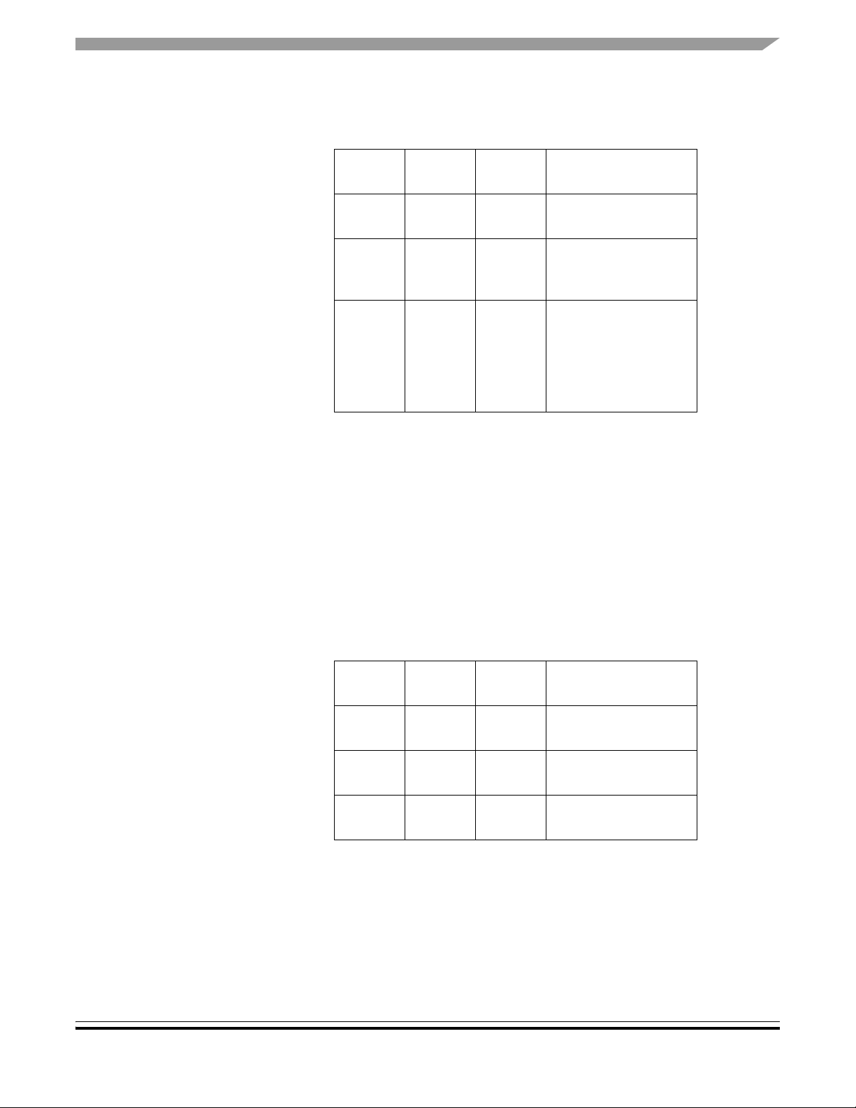
Table 1-4 Jumper Settings in EXT Power Mode
1.9.3 I/O Connector
Jumper
W1 2-3 5V
W2 1-2 EXT
W3 1-2 P_IO_5V
Default
Position
Setting Description
Sets the board for 5V
operation
Sets the board to be
wered externally
po
through J1
Outputs 5V on pin 1 of
the I/O
This jumper should be
removed if you do not
want to output 5V on
this pin.
connector, J35.
The DEMO9S08AC60E can also be powered through pin 1 of the I/O connector
J35. To power the board in this manner the jumper on W2 should be removed
and positive 5V DC should be applied on pin 1 of J35. This voltage input is not
regulated on the board so care should be taken to provide a clean 5V signal.
LED D1 will light green to let you know that power has been correctly applied
to the board. Jumper settings are detailed below
Table 1-5 Jumper Settings in I/O Connector Power Mode
Jumper
W1 2-3 5V
W2 Removed
W3 1-2 P_IO_5V
DEMO9S08AC60E User’s Guide, Rev. 0.1
Freescale Semiconductor 15
Default
Position
Setting Description
Sets the board for 5V
operation
Removes USB and
EXT power options
Inputs 5V on pin 1 of
the I/O
connector, J35
Page 16

1.9.4 3 Volt Operation
1.10 Reset Switch
1.11 Clock Source
The DEMO9S08AC60E can be run with VDD set to either 5 volts or 3 volts. To
run the board at 3V when using any of the three power options, move jumper
W1 to the 1-2, 3V position.
The reset switch (SW6) provides a way to apply a reset to the MCU. The reset
switch is connected directly to the RESET_B signal of the MCU. A 10K pull up
resistor to VDD on the RESET_B signal allows for normal operation. When the
reset switch is pressed the RESET_B signal is grounded and the MCU
recognizes a reset.
An on-board 4MHz crystal (Y1) is connected between the XTAL and EXTAL
pins of the MCU. There is also an option for the user to add a canned oscillator
to the board. To add an oscillator, the zero ohm resistors R18 and R20 should
be removed and an oscillator should be installed in the J2 footprint. This
footprint accepts either 14 pin or 8 pin oscillators. To go back to the crystal
option, the oscillator should be removed from J2 and zero ohm resistors should
be reinstalled in the R18 and R20 footprints.
1.12 RS-232
An RS-232 translator provides RS-232 communication on com connector J34.
This connector is a 9 pin Dsub right angle connector. TXD and RXD signals are
routed from the MCU to the RS-232 transceiver.
Table 1-6 RS-232 Connections
MCU Port Jumper COM Signal I/O Port Connector
PTE0/TXD1 J14 TXD OUT J34-2
PTE1/RXD1 J15 RXD IN J34-3
To disconnect port pins PTE0 and PTE1 from the RS-232 translator, remove
jumpers J14 and J15. The full pinout of the COM connector (J34) is listed below
DEMO9S08AC60E User’s Guide, Rev. 0.1
16 Freescale Semiconductor
Page 17
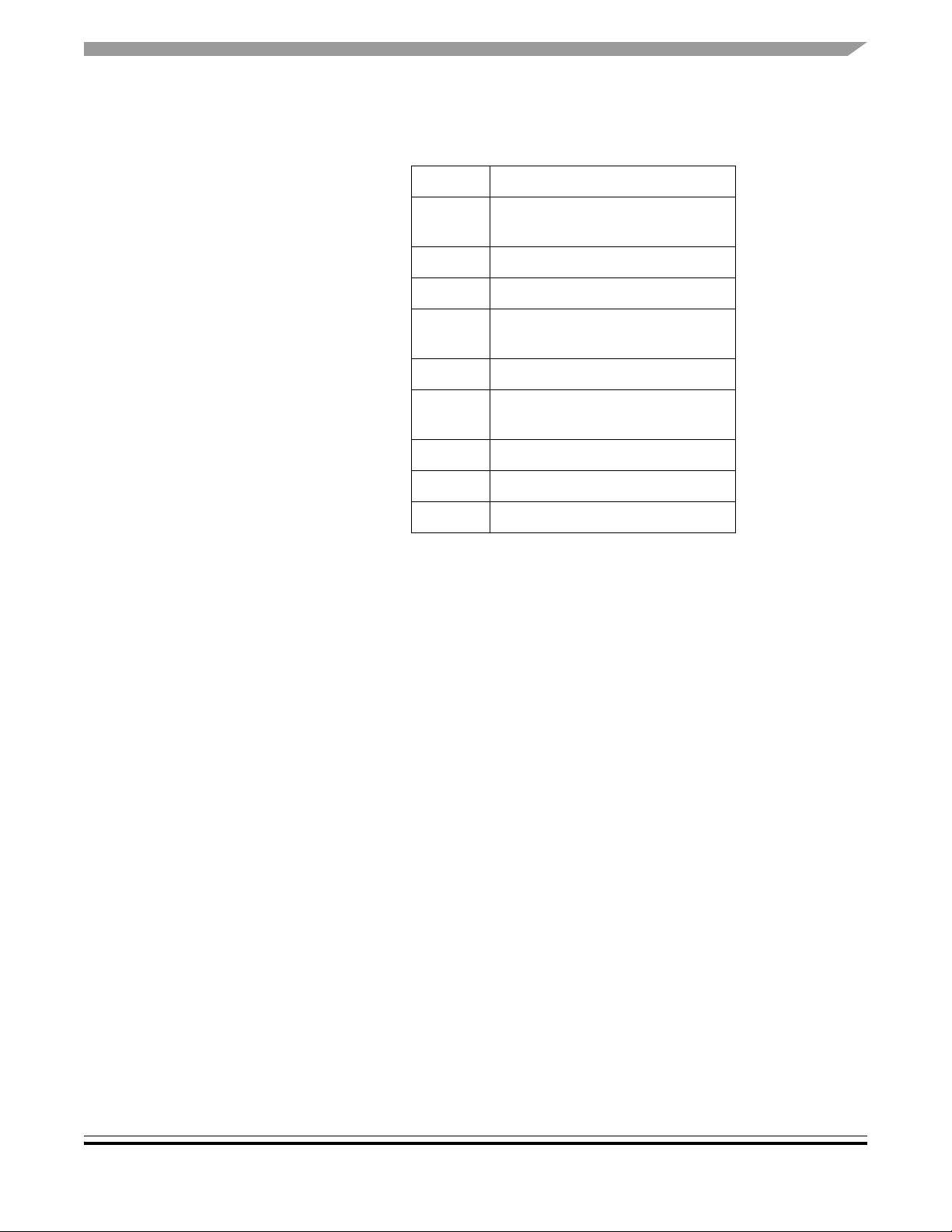
Table 1-7 COM Connector (J34) Pinout
Pin Signal Name
1.13 User Options
1
2 TXD
3 RXD
4
5 GND
6
7 NC
8 NC
9 NC
Connected to pins 4 and 6 through
z
ero ohm resistors R55 and R56
Connected to pins 1 and 6 through
ero ohm resistors R55 and R56
z
Connected to pins 1 and 4 through
ero ohm resistors R55 and R56
z
The DEMO9S08AC60E includes various user input and output devices to assist
in application development and silicon evaluation. These devices include four
pushbutton switches, a 10 LED light bar, 8 rocker switches, an accelerometer,
a light sensor, and a potentiometer.
1.13.1 Pushbutton Switches
Four pushbutton switches provide momentary active low input for user
applications. MCU port pins can be disconnected from these pushbutton
DEMO9S08AC60E User’s Guide, Rev. 0.1
Freescale Semiconductor 17
Page 18
1.13.2 Light Bar
switches by removing the appropriate jumper. The table below describes the
pushbutton switch connections
Table 1-8 Pushbutton Switch (SW1 - SW4) Connections
Switch MCU Port Jumper
SW1 PTC2 J12
SW2 PTC6 J13
SW3 PTD3 J11
SW4 PTD2 J10
A 10 red LED light bar (LED1) is provided to assist users during code
development. The LEDs are active low and are illuminated when a logic low
signal is driven from the MCU port pin. Eight of the LEDs on the light bar are
connected to port F. The other two are spare and are user assignable. They are
connected to test pads on the board that a user can solder to a desired port pin
or other signal. Port F pins can be disconnected from the light bar by removing
the appropriate jumper. The light bar is connected as described below
Table 1-9 Light Bar (LED1) Connections
LED MCU Port Jumper
LED0 PTF0 J16
LED1 PTF1 J17
LED2 PTF2 J18
LED3 PTF3 J19
LED4 PTF4 J20
LED5 PTF5 J21
LED6 PTF6 J22
LED7 PTF7 J23
LED8 NC JP4
LED9 NC JP5
DEMO9S08AC60E User’s Guide, Rev. 0.1
18 Freescale Semiconductor
Page 19

1.13.3 Rocker Switches
Eight rocker switches (SW5) are provided for user application development.
These switches are active low and input a logic low when set to the closed
position. There are no external pullups on these switches so the internal pullups
should be enabled on the MCU port pins to ensure proper operation. Port A pins
can be disconnected from the rocker switches by removing the appropriate
jumper. The rocker switches are connected as described below
Table 1-10 Rocker Switch (SW5) Connections
Switch MCU Port Jumper
1 PTA0 J24
2 PTA1 J25
3 PTA2 J26
4 PTA3 J27
5 PTA4 J28
6 PTA5 J29
1.13.4 Accelerometer
7 PTA6 J30
8 PTA7 J31
A Freescale MMA6270QT accelerometer (U5) is provided to assist users in
developing accelerometer based application code. The MMA6270QT provides
output data in the X and Y direction and has a sleep mode. The MMA6270QT
is a 3.3V part and is connected to the MC9S08AC60 through the use of a level
translator. The X and Y outputs are connected back to the MCU both directly
from the accelerometer (3.3V signals) and amplified to 5V through the use of
op-amps. The sleep mode is an active low input to the accelerometer. When a
logic low is applied to the sleepmode pin the device outputs are turned off,
providing significant reduction of operating current (low to 3 uA typically). The
MCU port pins can be disconnected from the accelerometer by removing the
appropriate jumper. The accelerometer is connected as described below
DEMO9S08AC60E User’s Guide, Rev. 0.1
Freescale Semiconductor 19
Page 20

Table 1-11 Accelerometer (U5) Connections
1.13.5 Light Sensor
1.13.6 Potentiometer
Accelerometer
Function
Sleep Mode PTC4 J5
Amplified Y Output PTD4 J6
Amplified X Output PTD5 J7
Raw Y Output PTD6 J8
Raw X Output PTD7 J9
MCU Port Jumper
A photo detect IC (U4) combines a photodiode and a current amplifier on a
single IC to provide variable current. The light sensor is connected to the MCU
on PTD1. PTD1 can be disconnected from the light sensor by removing jumper
J4.
1.13.7 I/O Connector
A 10 Kohm thumb-wheel potentiometer (VR1) provides variable resistor for
users to assist them in application development. The potentiometer is connected
to the MCU on PTD0. PTD0 can be disconnected from the potentiometer by
removing jumper J3. The voltage seen on PTD0 is the result of a voltage divider
that changes as the potentiometer is turned.
A 40-pin I/O connector (J35) is available for user expansion. This connector is
located on the bottom of the board and has holes so that pins of a connecting
DEMO9S08AC60E User’s Guide, Rev. 0.1
20 Freescale Semiconductor
Page 21

board can pass through the top of the board. The I/O connector is pinned out as
follows:
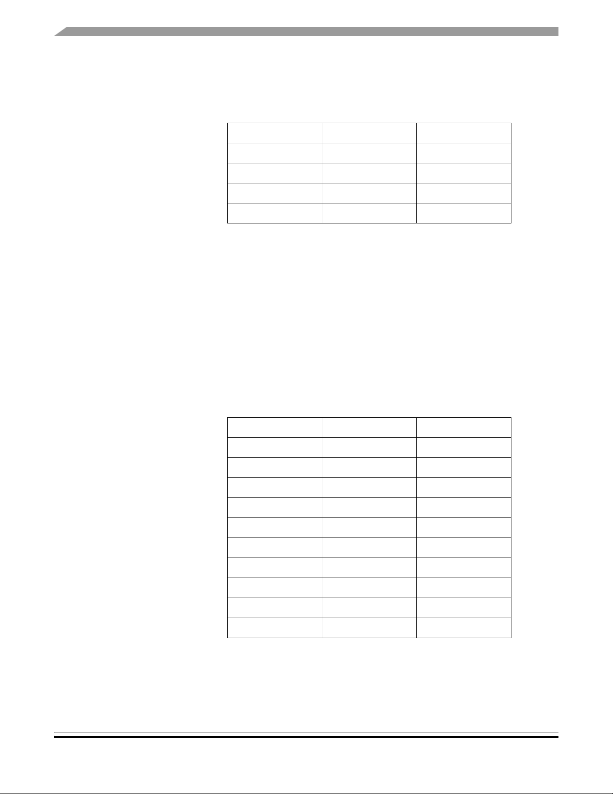
Table 1-12 I/O Connector (J35) Pinout
P_IO_5V 1 2 IRQ
GND 3 4 RESET_B
PTE0 5 6 BKGD
PTE1 7 8 PTG4
PTG0 9 10 PTB0
PTG1 11 12 PTB1
PTE2 13 14 PTB2
PTE3 15 16 PTB3
PTE6 17 18 PTB4
PTE5 19 20 PTB5
PTE7 21 22 PTB6
PTE4 23 24 PTB7
PTA0 25 26 PTC1
PTA1 27 28 PTC0
PTA2 29 30 PTG2
PTA3 31 32 PTG3
PTA4 33 34 PTF4
PTA5 35 36 PTF5
PTA6 37 38 PTC5
PTA7 39 40 PTC3
DEMO9S08AC60E User’s Guide, Rev. 0.1
Freescale Semiconductor 21
Page 22

DEMO9S08AC60E User’s Guide, Rev. 0.1
22 Freescale Semiconductor
Page 23

Page 24

How to Reach Us:
USA/Europe/Locations not listed:
Freescale Semiconductor Literature Distribution
P.O. Box 5405, Denver, Colorado 80217
1-800-521-6274 or 480-768-2130
Japan:
Freescale Semiconductor Japan Ltd.
SPS, Technical Information Center
3-20-1, Minami-Azabu
Minato-ku
Tokyo 106-8573, Japan
81-3-3440-3569
Asia/Pacific:
Freescale Semiconductor H.K. Ltd.
2 Dai King Street
Tai Po Industrial Estate
Tai Po, N.T. Hong Kong
852-26668334
Learn More:
For more information about Freescale Semiconductor
products, please visit
http://www.freescale.com
Information in this document is provided solely to enable system and software implementers to use Freescale
Semiconductor products. There are no express or implied copyright licenses granted hereunder to design or
fabricate any integrated circuits or integrated circuits based on the information in this document.
Freescale Semiconductor reserves the right to make changes without further notice to any products herein.
Freescale Semiconductor makes no warranty, representation or guarantee regarding the suitability of its
products for any particular purpose, nor does Freescale Semiconductor assume any liability arising out of the
application or use of any product or circuit, and specifically disclaims any and all liability, including without
limitation consequential or incidental damages. “Typical” parameters which may be provided in Freescale
Semiconductor data sheets and/or specifications can and do vary in different applications and actual
performance may vary over time. All operating parameters, including “Typicals” must be validated for each
customer application by customer’s technical experts. Freescale Semiconductor does not convey any license
under its patent rights nor the rights of others. Freescale Semiconductor products are not designed, intended,
or authorized for use as components in systems intended for surgical implant into the body, or other
applications intended to support or sustain life, or for any other application in which the failure of the Freescale
Semiconductor product could create a situation where personal injury or death may occur. Should Buyer
purchase or use Freescale Semiconductor products for any such unintended or unauthorized application, Buyer
shall indemnify and hold Freescale Semiconductor and its officers, employees, subsidiaries, affiliates, and
distributors harmless against all claims, costs, damages, and expenses, and reasonable attorney fees arising out
of, directly or indirectly, any claim of personal injury or death associated with such unintended or unauthorized
use, even if such claim alleges that Freescale Semiconductor was negligent regarding the design or
manufacture of the part.
Freescale™ and the Freescale logo are trademarks of Freescale Semiconductor, Inc. All other product or
service names are the property of their respective owners.
© Freescale Semiconductor, Inc. 2004.
DEMO9S08AC60EUG
Rev. 0.1, 11/2007
 Loading...