

Page 1

CSM-56F801
Development Module for Freescale DSP56F801
Page 2

DOC-0334-010, REV D DECEMBER 2, 2005
Freescale Semiconductor, Inc.
CONTENTS
CAUTIONARY NOTES ..............................................................................................................3
TERMINOLOGY.........................................................................................................................3
CSM-56F801..............................................................................................................................4
GETTING STARTED..................................................................................................................5
REFERENCE DOCUMENTATION.............................................................................................5
CSM-56F801 OPERATION........................................................................................................6
MEMORY MAP......................................................................................................................6
POWER SUPPLY.................................................................................................................. 7
PWR.................................................................................................................................. 7
CONNECTOR J1............................................................................................................... 7
PWR_SEL.........................................................................................................................8
RESET SWITCH ................................................................................................................... 8
LOW-VOLTAGE DETECT..................................................................................................... 8
TIMING.................................................................................................................................. 9
COMMUNICATIONS............................................................................................................. 9
COM CONNECTOR......................................................................................................... 9
USER OPTIONS ................................................................................................................. 10
I/O CONNECTORS............................................................................................................. 10
JTAG / ONCE.................................................................................................................. 10
J1 CONNECTOR............................................................................................................. 11
APPENDIX A............................................................................................................................12
MECHANICAL DETAILS..................................................................................................... 12
APPENDIX B............................................................................................................................13
BILL OF MATERIALS.......................................................................................................... 13
FIGURES
Figure 1: PWR_SEL Jumper Settings.........................................................................................8
Figure 2: COM Connector........................................................................................................10
Figure 3: JTAG / OnCE BDM Connection.................................................................................11
Figure 4: MCU I/O Connector...................................................................................................11
TABLES
Table 1: Program Memory Map..................................................................................................6
Table 2: Data Memory Map........................................................................................................7
Table 3: COM Signal Connections ............................................................................................9
Table 4: User Option Jumper Settings......................................................................................10
2
Page 3

DOC-0334-010, REV D DECEMBER 2, 2005
Freescale Semiconductor, Inc.
REVISION
Date Rev Comments
December 2, 2005 C Updated format and revision
CAUTIONARY NOTES
1) Electrostatic Discharge (ESD) prevention measures should be used when handling this
product. ESD damage is not a warranty repair item.
2) Axiom Manufacturing does not assume any liability arising out of the application or use of
any product or circuit described herein; neither does it convey any license under patent
rights or the rights of others.
3) EMC Information on the CSM-56F801 module:
a) This product as shipped from the factory with associated power supplies and cables, has
been verified to meet with requirements of CE and the FCC as a CLASS B product.
b) This product is designed and intended for use as a development platform for hardware
or software in an educational or professional laboratory.
c) In a domestic environment, this product may cause radio interference in which case the
user may be required to take adequate prevention measures.
d) Attaching additional wiring to this product or modifying the products operation from the
factory default as shipped may effect its performance and cause interference with nearby
electronic equipment. If such interference is detected, suitable mitigating measures
should be taken.
TERMINOLOGY
This development module uses option selection jumpers and cut-traces to setup default
configuration. Terminology for application of the option jumpers is as follows:
Jumper – a plastic shunt that connects 2 terminals electrically
Jumper on, in, or installed - jumper is installed such that 2 pins are connected together
Jumper off, out, or idle - jumper is installed on 1 pin only. It is recommended that
jumpers be idled by installing on 1 pin so they will not be lost.
Cut-Trace – a circuit trace connection between component pads. The circuit trace may
be cut using a razor knife to break the default connection. To reconnect the circuit,
simply install a suitably sized 0-ohm resistor or attach a wire across the pads.
3
Page 4
DOC-0334-010, REV D DECEMBER 2, 2005
Freescale Semiconductor, Inc.
CSM-56F801
The CSM-56F801 is an evaluation or demonstration board for the DSP56F801 digital signal
processor. The included wall plug, DB9 serial cable, sample software tools, examples, and
debug monitor make application development quick and easy. A JTAG port is provided for
development tool application and is compatible with JTAG interface cables and software. A
40-pin MPU I/O connector allows connecting the CSM-56F801 module to an expanded
evaluation environment.
FEATURES
• DSP56F801 DSP, 48 LQFP
• 40 MIPS
• 16K Byte Data Flash
• 4K Byte Program Flash
• 2K Byte Boot Flash
• 2K Byte Data RAM
• 2K Byte Program RAM
• Low-Voltage Interrupt
• Internal Relaxation Oscillator
• 2 General Purpose Quad Timers
• 11 I/O Lines
• Embedded PLL
• SCI and SPI Ports
• JTAG/OnCE Port
• Two 4-Ch, 12-bit ADC
• 6-Ch, 15-bit Edge- or Center-Aligned PWM
• 40 pin connector provides access to MPU I/O signals
• Power Input Selection Jumper
• Regulated +3.3V power supply
• Optional power input from MPU I/O Port connector
• Optional power output through MPU I/O Port connector
• Optional Ceramic Resonator
• RS-232 Serial Port w/ DB9 Connector
• User Components Provided
• 3 Push Button Switches: 2 User, RESET
• 3 LED Indicators: 2 User, VDD
• Jumpers
• Disable User Functions
• Power Select
• Connectors
• 40-pin Connector
• 2.0mm Barrel Connector Power Input
• JTAG Connector
• DB9 Communications Connector
• Supplied with DB9 Serial Cable, Documentation (CD), Manual, and Wall plug type power supply.
Specifications:
Module Size 2.2” x 1.6”
Power Input: +9VDC @ 200 mA typical, +4 to +16VDC range
4
Page 5

DOC-0334-010, REV D DECEMBER 2, 2005
Freescale Semiconductor, Inc.
GETTING STARTED
The CSM-56F801 single board computer is a fully assembled, fully functional development
module for the Freescale DSP56F801 digital signal processor. The module comes with a
serial cable, power supply, and installed binary monitor for stand-alone operation. Support
software for this development module is provided for Windows 95/98/NT/2000/XP operating
systems.
Users should be familiar with the hardware and software operation of the target MPU. Refer to
the DSP56F801 User Manual and Reference Manual for details on MPU operation. The
module’s purpose is to promote the features of the DSP56F801 and to assist the user in
quickly developing an application in a known working environment. Users should be familiar
with memory mapping, memory types, and embedded software design for quick, successful,
application development.
Use of the CSM-56F801 module requires Metrowerks CodeWarrior for Freescale DSP and an
Axiom Manufacturing JTAG cable. Both items are available in the CSM-56F801KIT. The
JTAG cable supports communications between the CSM-56F801 module and a standard PC.
REFERENCE DOCUMENTATION
Reference documents are provided on the support CD in Acrobat Reader format.
CSM56F801_SCH_B.pdf CSM-56F801 Module Schematic Rev B
CSM56F801_UG.pdf CSM-56F801 User Guide (this document)
DSP56F801-7UM.pdf DSP56F80x Users Manual
DPSP56F801.pdf Technical Data Sheet
DSOP56F800.pdf DSOP56F800 Family Manual
AN1909.pdf Multiple Target Features Using CodeWarrior
5
Page 6

DOC-0334-010, REV D DECEMBER 2, 2005
Freescale Semiconductor, Inc.
CSM-56F801 OPERATION
The CSM-56F801 module provides input and output features to assist embedded application
development. Access to MPU port signals is available through connector J1. This connector
may also be used to input power to the module or to output power to attached modules. RS232 communications signals may also be input through connector J1. Care must be exercised
when using the J1 to power the module, as only regulated +3.3VDC (+/- 5%) should be
supplied to this connection
Five option jumpers and 3 cut-traces control module operation. Enabling a jumper option
requires installing a shunt across the associated header pins. Removing the shunt disables
the associated option. An option enabled by a cut-trace can be disabled by removing the
circuit trace between the cut-trace component pads. Use a sharp knife to cut the embedded
circuit trace. Be careful not to damage adjacent circuitry. To re-enable the option, simply
install a suitably sized 0-ohm resistor or piece of wire across the cut-trace component pads.
MEMORY MAP
The DSP56F801 utilizes two independent memory spaces, data and program, configured in a
Harvard architecture. RAM and Flash memory are used for on-chip data memory and on-chip
program memory. Refer to the DSP56F801 User Guide for details on accessing Program and
Data memory.
Table 1: Program Memory Map
Program Memory – Mode 0A
0x0000 0x0003
0x0004 0x1FFF
0x 2000 0x7BFF
0x7C00 0x7FFF
0x8000 0x87FF
0x8800 –
0xFFFF
Boot Flash
Program Flash
Reserved
Program RAM
Boot Flash
Reserved
NOTE: The first 4 logical addresses are a reflection of the first 4 physical addresses
of Boot Flash
6
Page 7

DOC-0334-010, REV D DECEMBER 2, 2005
Freescale Semiconductor, Inc.
Table 2: Data Memory Map
Ex = 0
0x0000 –
Data RAM
0x3FFF
0x4000 –
Reserved
0xBFFF
0xC000 –
Peripherals
0x0FFF
0x1000 –
Data Flash
0x17FF
0x1800 –
Reserved
0xFF7F
0xFF80 –
Core Registers
0xFFFF
NOTE: EX = 1 address external memory. This function is not supported for the
DSP56F801.
Power Supply
Power is supplied to the module through a 2mm barrel connector at location PWR or through
connector J1. Power may also be sourced off-module through connector J1. The PWR_SEL
jumper determines the source of input power.
PWR
The PWR barrel connector accepts 2.0 – 2.1 mm barrel plug and allows the module to be
powered from a transformer plugged into a standard wall outlet. Input voltage should be limited
to between +4VDC and +12VDC. Input voltage of +9VDC @ 200 mA is typical.
Connector J1
Power may be supplied to the module through the pins J1-1 and J1-2. Use of this option
requires a regulated voltage input limited to +3.3VDC (+/- 5%). This input is connected directly
to the module power and ground planes. Care should be exercised not to over-drive this input.
This connection may also be used to power external modules attached to connector J1. The
PWR_SEL option header determines how power is routed to the module.
7
Page 8

DOC-0334-010, REV D DECEMBER 2, 2005
Freescale Semiconductor, Inc.
PWR_SEL
The PWR_SEL jumper selects the source of power input to the DSP-56F801 module or allows
regulated +3.3VDC to be provided to J1 for use by external circuits. The module may be
powered from the 2.0mm barrel connector (PWR) or from the 40-pin MCU connector (J1).
Power input at the PWR jack must be DC voltage between +5V and +16V. Power input on the
MCU connector must be regulated voltage between +3.0VDC and +3.3VDC. The
MCU_PORT connector input allows use of batteries, or other alternate sources, to power the
module. Damage may occur if the MCU_PORT power input pins are over-driven. Refer to the
table below to determine correct PWR_SEL jumper setting.
CAUTION: Module damage may occur if the MCU_PORT power input pin (J1-1) is over-driven.
The PWR_SEL option jumper provides 3 possible configurations; source power from the PWR
connector, source power from J1, or source power from PWR and supply power to J1. The
figures below show the settings for each configuration.
Figure 1: PWR_SEL Jumper Settings
1
• •
2 • •
1 • •
2 • •
1 • •
2 • •
Module powered from external +3.0VDC - +3.3VDC input
connected to J1-1 (+) and J1-3 (-)
Module powered from external +5VDC - +16VDC connected to
PWR Terminal Block. J1-1 is open or not connected.
Module powered from external +3.0VVDC - +3.3VDC connected
to J1-1 (+) and J1-3 (-). Module provides +3.3VDC output (up to
50 mA) at pin J1 for use by external circuits.
Reset Switch
The RESET switch provides a method to apply an asynchronous reset to the module.
Pressing the RESET switch applies a low voltage level to the RESET input. Logic on this
signal prevents unwanted RESET inputs to the MPU.
Low-Voltage Detect
The MPU includes an internal POR and Low-Voltage Interrupt circuit. This circuit protects
against low-voltage and under-voltage conditions. The system consists of a POR circuit and a
low-voltage interrupt (LVI) circuit. The POR circuit holds the MPU in reset until voltage
reaches an acceptable level. The LVI provides an interrupt out when voltage falls below the
trip level. Refer to the MPU User Guide for further details.
8
Page 9

DOC-0334-010, REV D DECEMBER 2, 2005
Freescale Semiconductor, Inc.
Timing
The MPU function from either an internal relaxation oscillator or an external timing source. A
location for an external timing source has been provided. Component size for the external
timing source is based on an 8 MHz ceramic resonator from Panasonic, P/N EFO-S8004E5A.
This part is not populated in the default module configuration. Refer to the MPU User Guide for
further details
Communications
The CSM-56F801 module provides a single RS-232 communications port. An RS-232
transceiver (U2) provides RS-232 signal level to TTL/CMOS logic level translation on the first
RS-232 channel. RS232 signals TXD0 and RXD0 are routed between the transceiver and the
MCU. These signals are also routed to connector J1. RS-232 communication signals input on
J1 must be TTL/CMOS logic levels; no translation support is provided through this path. The
transceiver output may also be driven off-module if the signals are suitably buffered. As added
development support, hardware flow control signals RTS and CTS are available on the logic
side of U2. These signals are routed to vias located near the transceiver (U2). RTS has been
biased properly to support 2-wire RS-232 communications.
Use of the J1 connector to input RS-232 signals requires disabling the on-board RS-232
transceiver. Otherwise, signal corruption may occur. Disabling the on-board transceiver is
accomplished by opening cut-traces CT4, and CT5. Simply remove the circuit trace between
the cut-trace pads to open the circuit. To restore the circuit functionality, install a 1206 size, 0ohm, resistor or a short piece of wire across the cut-trace pads.
Table 3: COM Signal Connections
COM Signal MPU Port Connector
J1
TXD0 GPIOB0/TXD0 5 CT4
RXD0 GPIOB1/RXD0 7 CT4
Signal
Disable
COM Connector
A standard 9-pin Dsub connector provides external connections for the COM port. The COM
port is used by default with the debug monitor. Component U2 provides RS-232 translation
services. The figure below details the DB9 connector.
9
Page 10

DOC-0334-010, REV D DECEMBER 2, 2005
Freescale Semiconductor, Inc.
Figure 2: COM Connector
Female DB9 connector that interfaces to the MPU serial port
via the U2 RS232 transceiver. It provides simple 2 wire
asynchronous serial communications without flow control.
Flow control is provided at test points on the module.
Pins 1, 4, and 6 are connected together.
TXD
RXD
GND
1
6
2
3
4
5
RTS
7
CTS
8
NC
9
User Options
Indicators LED1 and LED2 are connected to the MPU I/O ports by the USER option bank.
When the appropriate USER jumper is installed, the assigned LED is active. Each LED is
active low. A low voltage level driven out on the appropriate MPU port causes the LED to light.
MPU ports PWMA0 and PWMA1 drive LED1 and LED2 respectively.
Two push button switches provide momentary, active low, input to the MPU for user
applications. Switches SW1 and SW2 are connected to the MPU I/O ports by the USER
option bank. SW1 and SW2 provide input to MCUI/O ports TD0 and TD1 respectively. The
table below shows the user jumper settings.
Table 4: User Option Jumper Settings
Jumper On Off MPU Signal
User 1 Enable SW1 Disable SW1 PWMA0
User 2 Enable SW2 Disable SW2 PWMA1
User 3 Enable LED1 Disable LED1 TD0
User 4 Enable LED2 Disable LED2 TD1
I/O Connectors
JTAG / OnCE
The JTAG/OnCE 14 pin connector is compatible with the Freescale On Chip Emulation
(OnCE) development port. This connector allows the connection of a OnCE style background
debug cable for software development, programming and debugging in real-time.
10
Page 11

DOC-0334-010, REV D DECEMBER 2, 2005
Freescale Semiconductor, Inc.
Figure 3: JTAG / OnCE BDM Connection
TDI
TDO
TCK
/RESET
V
DD
/DE
1 2
3 4
5 6
7 8
9 10
11 12
13 14
GND
GND
GND
N/C (key)
TMS
/TRST
J1 Connector
Connector J1 provides access to CSM-56F801 I/O port signals. This connector may also be
used to power the module or to power off-module circuitry.
Figure 4: MCU I/O Connector
V
GND
TxD0
RxD0
TD0
TD1
TD2
MOSI
MISO
SCLK
SS*
ANA2
ANA3
ANA4
ANA5
ANA6
ANA7
X
11 12
13 14
15 16
17 18
19 20
21 22
23 24
25 26
27 28
29 30
31 32
33 34
35 36
37 38
39 40
1 2
3 4
5 6
7 8
9 10
IREQA* Default Signal Assignment
RESET* MCU Port Signal Disable
TxD0 COM1 TXD CT-4
RxD0 COM1 RXD CT-5
TD0 SW1 User1
TD1 SW2 User2
PWMA0 LED1 User3
ANA0 PWMA1 LED2 User4
ANA1
Note: Default signal assignment
FAULTA0
should be disabled to use the signal
at connector J1
PWMA0
PWMA1
PWMA2
PWMA3
PWMA4
PWMA5
11
Page 12

DOC-0334-010, REV D DECEMBER 2, 2005
Freescale Semiconductor, Inc.
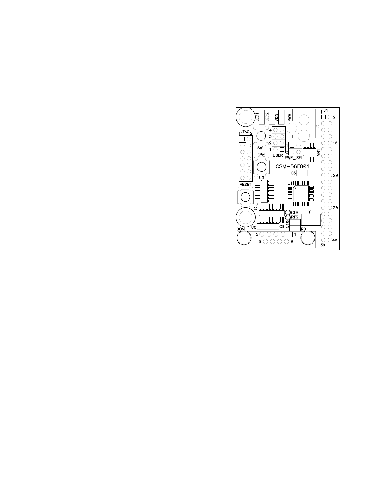
APPENDIX A
Mechanical Details
12
Page 13

CSM-56F801 OCTOBER 4, 2004
13
APPENDIX B
BILL OF MATERIALS
Qty Title Ref(m) Mfr Mfr-P/N
BOM, CSM56F801, AXM-0334
1 3 Cap, Tant, 10uF, 10V, SMB C12, C15, C17 Avx TAJB106K010R
2 2 Cap, Mon, 2.2uF, 16V, 0805, SMT C5, C10
3 5 Cap, Mon, 1uF, 16V, 0805 C2, C6, C7, C8, C9
4 7 Cap, Mon, .1uF, 50V, 0805 C1, C4, C13, C14, C16, C18, C19 Meritek MA080525U104M5
00
5 5 Res, Carbon, 10K ohm, 5%, 0805 R1,R8, R12, R13, R14
6 3 Res, Carbon, 47K ohm, 5%, 0805 R5, R6, R7
7 1 Res, Carbon, 820 ohm, 5%, 0805 R4
8 3 Res, Carbon, 470 ohm, 1/16W, 5%, 0805 R2, R3, R11
9 1 Diode, Schottky, 30V, 200mA, BAT54C, Com.
Cathode, SOT23
D1 Vishay BAT54C
10 3 LED, Green, w/reflector, 1206, SMT LED1, LED2, VDD Rohm SML-010MTT86
11 1 Ind, 10uH, 1210, SMT L1 Vishay IMC1210SY100K
12 1 IC, Quad 2 Input NAND, 14SOIC, 74AC00 U3 TI SN74AC00DR
13 1 IC, Dual RS232 XCVR, 3.3V, ESD, 16SOIC U2 Intersil ICL3232ECBN
14 1 IC, DSP, 56F801FA, 48LQFP U1 Freescale DSP56F801FA
15 1 VReg, LDO, 3.3V, 250mA, 8 SOIC VR1 STM L4931CD33
16 3 Sw, PB, 5mm Sq, Thru RESET, SW1, SW2
17 5 Hdw, Shunt, 2 Pos, .1"
18 1 Conn, 2.1mm, Pwr Jack, Barrel, Thru, RA PWR
19 1 Conn, Dsub, 9P, F, RA, PCB Mount COM
20 1 Conn, 2x2 Pin Header, .1" Ctr, Thru PWR_SEL
21 1 Conn, 2x4 Pin Header, .1" Ctr, Thru USER
22 1 Conn, 2x7 Pin Header, .1" Ctr, Thru JTAG
23 1 Conn, 2X20 Pin Header, .1" Ctr, Thru J1
Freescale Semiconductor, Inc.
Page 14

CSM-56F801 OCTOBER 4, 2004
14
24 0 Do Not Install Components R9, Y1
25 1 PCB, CSM56F801 Module, 1.6x2.2 in, 2-sided
Freescale Semiconductor, Inc.
 Loading...