

Page 1

Freescale Semiconductor, Inc.
CPU32
REFERENCE MANUAL
nc...
I
cale Semiconductor,
Motorola reserves the right to make changes without further notice to any products herein. Motorola makes no warranty, representation or guarantee regarding the suitability
of its products for any particular purpose, nor does Motorola assume any liability arising out of the application or use of any product or circuit, and specifically disclaims any and
all liability, including without limitation consequential or incidental damages. "Typical" parameters can and do vary in different applications. All operating parameters, including
Frees
"Typicals" must be validated for each customer application by customer's technical experts. Motorola does not convey any license under its patent rights nor the rights of others.
Motorola products are not designed, intended, or authorized for use as components in systems intended for surgical implant into the body, or other applications intended to
support or sustain life, or for any other application in which the failure of the Motorola product could create a situation where personal injury or death may occur. Should Buyer
purchase or use Motorola products for any such unintended or unauthorized application, Buyer shall indemnify and hold Motorola and its officers, employees, subsidiaries,
affiliates, and distributors harmless against all claims, costs, damages, and expenses, and reasonable attorney fees arising out of, directly or indirectly, any claim of personal
injury or death associated with such unintended or unauthorized use, even if such claim alleges that Motorola was negligent regarding the design or manufacture of the part.
MOTOROLA and ! are registered trademarks of Motorola, Inc. Motorola, Inc. is an Equal Opportunity/Affirmative Action Employer.
© MOTOROLA, INC., 1990, 1996
For More Information On This Product,
Go to: www.freescale.com
Page 2

Freescale Semiconductor, Inc.
nc...
I
cale Semiconductor,
Frees
For More Information On This Product,
Go to: www.freescale.com
Page 3

Freescale Semiconductor, Inc.
PREFACE
This reference manual describes programming and operation of the CPU32 instruction processing module, found in the M68300 Family of embedded controllers.
It is part of a multivolume set of manuals — each volume corresponds to a major
module in the M68300 Family.
A user's manual for each device incorporating the CPU32 describes processor
function and operation with reference to other modules within the device.
This manual consists of the following sections and appendix:
Section 1 Overview
Section 2 Architecture Summary
Section 3 Data Organization and Addressing Capabilities
nc...
I
cale Semiconductor,
Frees
Section 4 Instruction Set
Section 5 Processing States
Section 6 Exception Processing
Section 7 Development Support
Section 8 Instruction Execution Timing
Appendix A M68000 Family Summary
Index
NOTE
In this manual, the terms assertion and negation specifya particular
logic state.
Negate and negation refer to an inactive or false signal. These
terms are used independently of the voltage level that they represent.
This manual is written for systems designers, systems programmers, and applications programmers. Systems designers need general knowledge of the entire volume, with particular emphasis on Section 1, Section 7, and Appendix A — they will
also need to be familiar with electrical specifications and mechanical data contained in the user’s manual. Systems programmers should become familiar with
Sections 1 through 6, Section 8, and Appendix A. Applications programmers can
find most of the information they need in Sections 1 through 5, Section 8, and Appendix A.
Assert and assertion refer to an active or true signal.
This manual is also written for users of the M68000 Family that are not familiar with
the CPU32. Although there are comparative references to other Motorola microprocessors throughout the manual, Section 1, Section 2, and Appendix A specifically identify the CPU32 within the M68000 Family, and discuss the differences
betweeen it and related devices.
CPU32 REFERENCE MANUAL MOTOROLA
For More Information On This Product,
Go to: www.freescale.com
iii
Page 4

Freescale Semiconductor, Inc.
nc...
I
cale Semiconductor,
Frees
MOTOROLA CPU32 REFERENCE MANUAL
iv
For More Information On This Product,
Go to: www.freescale.com
Page 5

Freescale Semiconductor, Inc.
TABLE OF CONTENTS
Paragraph Title Page
SECTION 1 OVERVIEW
1.1 Features ....................................................................................................1-1
1.1.1 Virtual Memory ..................................................................................1-2
1.1.2 Loop Mode Instruction Execution ......................................................1-2
1.1.3 Vector Base Register ........................................................................1-3
1.1.4 Exception Handling ...........................................................................1-3
1.1.5 Enhanced Addressing Modes ...........................................................1-4
1.1.6 Instruction Set ...................................................................................1-4
1.1.6.1 Table Lookup and Interpolation Instructions .............................1-4
1.1.6.2 Low-Power Stop Instruction ......................................................1-6
nc...
I
1.1.7 Processing States .............................................................................1-6
1.1.8 Privilege States .................................................................................1-6
1.2 Block Diagram ...........................................................................................1-6
cale Semiconductor,
Frees
SECTION 2ARCHITECTURE SUMMARY
2.1 Programming Model ..................................................................................2-1
2.2 Registers ...................................................................................................2-2
2.3 Data Types ................................................................................................2-3
2.3.1 Organization in Registers ..................................................................2-4
2.3.1.1 Data Registers ..........................................................................2-4
2.3.1.2 Address Registers .....................................................................2-5
2.3.1.3 Control Registers ......................................................................2-5
2.3.2 Organization in Memory ....................................................................2-6
SECTION 3 DATA ORGANIZATION AND ADDRESSING CAPABILITIES
3.1 Program and Data References ..................................................................3-1
3.2 Notation Conventions ................................................................................3-2
3.3 Implicit Reference ......................................................................................3-2
3.4 Effective Address ......................................................................................3-3
3.4.1 Register Direct Mode .........................................................................3-3
3.4.1.1 Data Register Direct ..................................................................3-3
3.4.1.2 Address Register Direct ............................................................3-3
3.4.2 Memory Addressing Modes ...............................................................3-4
3.4.2.1 Address Register Indirect ..........................................................3-4
3.4.2.2 Address Register Indirect With Postincrement ..........................3-4
3.4.2.3 Address Register Indirect With Predecrement ..........................3-4
3.4.2.4 Address Register Indirect With Displacement ...........................3-5
3.4.2.5 Address Register Indirect With Index (8-Bit Displacement) ......3-5
3.4.2.6 Address Register Indirect With Index (Base Displacement) .....3-6
CPU32 MOTOROLA
REFERENCE MANUAL v
For More Information On This Product,
Go to: www.freescale.com
Page 6

Freescale Semiconductor, Inc.
TABLE OF CONTENTS
(Continued)
Paragraph Title Page
3.4.3 Special Addressing Modes ................................................................3-7
3.4.3.1 Program Counter Indirect With Displacement ...........................3-7
3.4.3.2 Program Counter Indirect with Index (8-Bit Displacement) .......3-7
3.4.3.3 Program Counter Indirect with Index (Base Displacement) ......3-8
3.4.3.4 Absolute Short Address ............................................................3-8
3.4.3.5 Absolute Long Address .............................................................3-9
3.4.3.6 Immediate Data .........................................................................3-9
3.4.4 Effective Address Encoding Summary ..............................................3-9
3.5 Programming View of Addressing Modes ...............................................3-11
3.5.1 Addressing Capabilities ...................................................................3-11
3.5.2 General Addressing Mode Summary ..............................................3-14
nc...
I
3.6 M68000 Family Addressing Capability ....................................................3-14
3.7 Other Data Structures .............................................................................3-15
3.7.1 System Stack ..................................................................................3-15
3.7.2 User Stacks .....................................................................................3-16
3.7.3 Queues ............................................................................................ 3-17
cale Semiconductor,
Frees
SECTION 4 INSTRUCTION SET
4.1 M68000 Family Compatibility ....................................................................4-1
4.1.1 New Instructions ................................................................................4-1
4.1.1.1 Low-Power Stop (LPSTOP) ......................................................4-1
4.1.1.2 Table Lookup and Interpolation (TBL) .......................................4-2
4.1.2 Unimplemented Instructions ..............................................................4-2
4.2 Instruction Format .....................................................................................4-2
4.2.1 Notation ............................................................................................. 4-3
4.3 Instruction Summary .................................................................................4-5
4.3.1 Condition Code Register ...................................................................4-5
4.3.2 Data Movement Instructions ..............................................................4-6
4.3.3 Integer Arithmetic Operations ............................................................4-7
4.3.4 Logic Instructions ..............................................................................4-8
4.3.5 Shift and Rotate Instructions .............................................................4-9
4.3.6 Bit Manipulation Instructions .............................................................4-9
4.3.7 Binary-Coded Decimal (BCD) Instructions ......................................4-10
4.3.8 Program Control Instructions ...........................................................4-10
4.3.9 System Control Instructions ............................................................4-11
4.3.10 Condition Tests ...............................................................................4-12
4.4 Instruction Details ....................................................................................4-13
4.5 Instruction Format Summary .................................................................4-170
4.6 Table Lookup and Interpolation Instructions .........................................4-188
4.6.1 Table Example 1: Standard Usage ...............................................4-188
4.6.2 Table Example 2: Compressed Table ...........................................4-189
MOTOROLA CPU32
vi REFERENCE MANUAL
For More Information On This Product,
Go to: www.freescale.com
Page 7

nc...
I
cale Semiconductor,
Frees
Freescale Semiconductor, Inc.
TABLE OF CONTENTS
(Continued)
Paragraph Title Page
4.6.3 Table Example 3: 8-Bit Independent Variable ...............................4-191
4.6.4 Table Example 4: Maintaining Precision .......................................4-192
4.6.5 Table Example 5: Surface Interpolations ......................................4-194
4.7 Nested Subroutine Calls ........................................................................4-194
4.8 Pipeline Synchronization with the NOP Instruction ...............................4-194
SECTION 5PROCESSING STATES
5.1 State Transitions .......................................................................................5-1
5.2 Privilege Levels .........................................................................................5-1
5.2.1 Supervisor Privilege Level .................................................................5-2
5.2.2 User Privilege Level ..........................................................................5-2
5.2.3 Changing Privilege Level ...................................................................5-2
5.3 Types of Address Space ...........................................................................5-3
5.3.1 CPU Space Access ..........................................................................5-3
5.3.1.1 Type 0000 — Breakpoint ..........................................................5-4
5.3.1.2 Type 0001 — MMU Access ......................................................5-4
5.3.1.3 Type 0010 — Coprocessor Access ...........................................5-4
5.3.1.4 Type 0011 — Internal Register Access .....................................5-4
5.3.1.5 Type 1111 — Interrupt Acknowledge ........................................5-5
SECTION 6 EXCEPTION PROCESSING
6.1 Definition of Exception Processing ............................................................6-1
6.1.1 Exception Vectors .............................................................................6-1
6.1.2 Types of Exceptions ..........................................................................6-2
6.1.3 Exception Processing Sequence .......................................................6-3
6.1.4 Exception Stack Frame .....................................................................6-3
6.1.5 Multiple Exceptions ...........................................................................6-4
6.2 Processing of Specific Exceptions ............................................................6-5
6.2.1 Reset ................................................................................................. 6-5
6.2.2 Bus Error ...........................................................................................6-6
6.2.3 Address Error ....................................................................................6-7
6.2.4 Instruction Traps ................................................................................6-8
6.2.5 Software Breakpoints ........................................................................6-8
6.2.6 Hardware Breakpoints .......................................................................6-8
6.2.7 Format Error ......................................................................................6-9
6.2.8 Illegal or Unimplemented Instructions ...............................................6-9
6.2.9 Privilege Violations ..........................................................................6-10
6.2.10 Tracing ............................................................................................6-11
6.2.11 Interrupts .........................................................................................6-12
6.2.12 Return from Exception .....................................................................6-13
CPU32 MOTOROLA
REFERENCE MANUAL vii
For More Information On This Product,
Go to: www.freescale.com
Page 8

nc...
I
cale Semiconductor,
Frees
Freescale Semiconductor, Inc.
TABLE OF CONTENTS
(Continued)
Paragraph Title Page
6.3 Fault Recovery ........................................................................................6-14
6.3.1 Types of Faults ................................................................................6-16
6.3.1.1 Type I: Released Write Faults .................................................6-16
6.3.1.2 Type II: Prefetch, Operand, RMW, and MOVEP Faults ..........6-17
6.3.1.3 Type III: Faults During MOVEM Operand Transfer .................6-17
6.3.1.4 Type IV: Faults During Exception Processing .........................6-18
6.3.2 Correcting a Fault ............................................................................6-18
6.3.2.1 (Type I) Completing Released Writes via Software ................6-19
6.3.2.2 (Type I) Completing Released Writes via RTE .......................6-19
6.3.2.3 (Type II) Correcting Faults via RTE .........................................6-19
6.3.2.4 (Type III) Correcting Faults via Software .................................6-20
6.3.2.5 (Type III) Correcting Faults By Conversion and Restart .........6-20
6.3.2.6 (Type III) Correcting Faults via RTE ........................................6-21
6.3.2.7 (Type IV) Correcting Faults via Software ................................6-21
6.4 CPU32 Stack Frames ..............................................................................6-21
6.4.1 Normal Four-Word Stack Frame .....................................................6-22
6.4.2 Normal Six-Word Stack Frame ........................................................6-22
6.4.3 BERR Stack Frame .........................................................................6-22
SECTION 7 DEVELOPMENT SUPPORT
7.1 CPU32 Integrated Development Support ..................................................7-1
7.1.1 Background Debug Mode (BDM) Overview ......................................7-1
7.1.2 Deterministic Opcode Tracking Overview .........................................7-2
7.1.3 On-Chip Hardware Breakpoint Overview ..........................................7-3
7.2 Background Debug Mode (BDM) ..............................................................7-3
7.2.1 Enabling BDM ...................................................................................7-4
7.2.2 BDM Sources ....................................................................................7-4
7.2.2.1 External BKPT Signal ................................................................7-4
7.2.2.2 BGND Instruction ......................................................................7-4
7.2.2.3 Double Bus Fault .......................................................................7-5
7.2.2.4 Peripheral Breakpoints ..............................................................7-5
7.2.3 Entering BDM ....................................................................................7-5
7.2.4 Command Execution .........................................................................7-5
7.2.5 Background Mode Registers .............................................................7-6
7.2.5.1 Fault Address Register (FAR) ...................................................7-6
7.2.5.2 Return Program Counter (RPC) ................................................7-6
7.2.5.3 Current Instruction Program Counter (PCC) .............................7-7
7.2.6 Returning from BDM ..........................................................................7-7
7.2.7 Serial Interface ..................................................................................7-7
7.2.7.1 CPU Serial Logic .......................................................................7-8
7.2.7.2 Development System Serial Logic ..........................................7-10
MOTOROLA CPU32
viii REFERENCE MANUAL
For More Information On This Product,
Go to: www.freescale.com
Page 9

nc...
I
cale Semiconductor,
Frees
Freescale Semiconductor, Inc.
TABLE OF CONTENTS
(Continued)
Paragraph Title Page
7.2.8 Command Set .................................................................................7-11
7.2.8.1 Command Format ...................................................................7-11
7.2.8.2 Command Sequence Diagram ................................................7-12
7.2.8.3 Command Set Summary .........................................................7-14
7.2.8.4 Read A/D Register (RAREG/RDREG) ....................................7-15
7.2.8.5 Write A/D Register (WAREG/WDREG) ...................................7-15
7.2.8.6 Read System Register (RSREG) ............................................7-16
7.2.8.7 Write System Register (WSREG) ...........................................7-16
7.2.8.8 Read Memory Location (READ) ..............................................7-17
7.2.8.9 Write Memory Location (WRITE) ............................................7-18
7.2.8.10 Dump Memory Block (DUMP) .................................................7-19
7.2.8.11 Fill Memory Block (FILL) .........................................................7-21
7.2.8.12 Resume Execution (GO) .........................................................7-22
7.2.8.13 Call User Code (CALL) ...........................................................7-22
7.2.8.14 Reset Peripherals (RST) .........................................................7-24
7.2.8.15 No Operation (NOP) ................................................................7-24
7.2.8.16 Future Commands ..................................................................7-25
7.3 Deterministic Opcode Tracking ...............................................................7-25
7.3.1 Instruction Fetch (IFETCH) .............................................................7-25
7.3.2 Instruction Pipe (IPIPE) ...................................................................7-25
7.3.3 Opcode Tracking during Loop Mode ...............................................7-27
SECTION 8 INSTRUCTION EXECUTION TIMING
8.1 Resource Scheduling ................................................................................8-1
8.1.1 Microsequencer ................................................................................. 8-1
8.1.2 Instruction Pipeline ............................................................................8-2
8.1.3 Bus Controller Resources .................................................................8-2
8.1.3.1 Prefetch Controller ....................................................................8-3
8.1.3.2 Write-Pending Buffer .................................................................8-3
8.1.3.3 Microbus Controller ...................................................................8-3
8.1.4 Instruction Execution Overlap ...........................................................8-4
8.1.5 Effects of Wait States ........................................................................8-5
8.1.6 Instruction Execution Time Calculation .............................................8-5
8.1.7 Effects of Negative Tails ....................................................................8-6
8.2 Instruction Stream Timing Examples .........................................................8-7
8.2.1 Timing Example 1: Execution Overlap ..............................................8-7
8.2.2 Timing Example 2: Branch Instructions .............................................8-8
8.2.3 Timing Example 3: Negative Tails .....................................................8-9
8.3 Instruction Timing Tables ........................................................................8-10
8.3.1 Fetch Effective Address ..................................................................8-12
8.3.2 Calculate Effective Address ............................................................8-13
CPU32 MOTOROLA
REFERENCE MANUAL ix
For More Information On This Product,
Go to: www.freescale.com
Page 10

Freescale Semiconductor, Inc.
TABLE OF CONTENTS
(Continued)
Paragraph Title Page
8.3.3 MOVE Instruction ............................................................................8-14
8.3.4 Special-Purpose MOVE Instruction .................................................8-14
8.3.5 Arithmetic/Logic Instructions ...........................................................8-15
8.3.6 Immediate Arithmetic/Logic Instructions ..........................................8-17
8.3.7 Binary-Coded Decimal and Extended Instructions ..........................8-18
8.3.8 Single Operand Instructions ............................................................8-18
8.3.9 Shift/Rotate Instructions ..................................................................8-19
8.3.10 Bit Manipulation Instructions ...........................................................8-20
8.3.11 Conditional Branch Instructions .......................................................8-20
8.3.12 Control Instructions .........................................................................8-21
8.3.13 Exception-Related Instructions and Operations ..............................8-21
nc...
I
8.3.14 Save and Restore Operations .........................................................8-22
cale Semiconductor,
Frees
APPENDIX AM68000 FAMILY SUMMARY
INDEX
MOTOROLA CPU32
x REFERENCE MANUAL
For More Information On This Product,
Go to: www.freescale.com
Page 11

nc...
I
cale Semiconductor,
Frees
Freescale Semiconductor, Inc.
LIST OF ILLUSTRATIONS
Figure Title Page
1-1 Loop Mode Instruction Sequence ...................................................................1-3
1-2 CPU32 Block Diagram ................................................................................... 1-7
2-1 User Programming Model .............................................................................. 2-2
2-2 Supervisor Programming Model Supplement .................................................2-2
2-3 Status Register ............................................................................................... 2-3
2-4 Data Organization in Data Registers .............................................................. 2-4
2-5 Address Organization in Address Registers ...................................................2-5
2-6 Memory Operand Addressing ........................................................................ 2-7
3-1 Single-Effective-Address Instruction Operation Word ....................................3-1
3-2 Effective Address Specification Formats ...................................................... 3-10
3-3 Using SIZE in the Index Selection ................................................................ 3-12
3-4 Using Absolute Address with Indexes ..........................................................3-12
3-5 Addressing Array Items ................................................................................3-13
3-6 M68000 Family Address Extension Words .................................................. 3-15
4-1 Instruction Word General Format ...................................................................4-2
4-2 Instruction Description Format ..................................................................... 4-14
4-3 Table Example 1 ........................................................................................ 4-188
4-4 Table Example 2 ........................................................................................ 4-189
4-5 Table Example 3 ........................................................................................ 4-191
6-1 Exception Stack Frame .................................................................................. 6-4
6-2 Reset Operation Flowchart .............................................................................6-6
6-3 Format $0 — Four-Word Stack Frame ......................................................... 6-22
6-4 Format $2 — Six-Word Stack Frame ........................................................... 6-22
6-5 Internal Transfer Count Register ..................................................................6-23
6-6 Format $C — BERR Stack for Prefetches and Operands ............................6-24
6-7 Format $C — BERR Stack on MOVEM Operand ........................................ 6-24
6-8 Format $C — Four- and Six-Word BERR Stack .......................................... 6-24
7-1 In-Circuit Emulator Configuration ................................................................... 7-2
7-2 Bus State Analyzer Configuration .................................................................. 7-2
7-3 BDM Block Diagram .......................................................................................7-3
7-4 BDM Command Execution Flowchart ............................................................ 7-6
7-5 Debug Serial I/O Block Diagram .................................................................... 7-8
7-6 Serial Interface Timing Diagram ..................................................................... 7-9
7-7 BKPT Timing for Single Bus Cycle ............................................................... 7-10
7-8 BKPT Timing for Forcing BDM .....................................................................7-10
7-9 BKPT/DSCLK Logic Diagram ....................................................................... 7-11
7-10 Command-Sequence-Diagram Example ...................................................... 7-13
7-11 Functional Model of Instruction Pipeline ....................................................... 7-26
7-12 Instruction Pipeline Timing Diagram ............................................................. 7-26
8–1 Block Diagram of Independent Resources .....................................................8-2
8-2 Simultaneous Instruction Execution ............................................................... 8-4
CPU32 MOTOROLA
REFERENCE MANUAL xi
For More Information On This Product,
Go to: www.freescale.com
Page 12

Freescale Semiconductor, Inc.
LIST OF ILLUSTRATIONS
(Continued)
Figure Title Page
8–3 Attributed Instruction Times ............................................................................ 8-4
8-4 Example 1 — Instruction Stream ....................................................................8-7
8-5 Example 2 — Branch Taken .......................................................................... 8-8
8-6 Example 2 — Branch Not Taken .................................................................... 8-8
8-7 Example 3 — Branch Negative Tail ............................................................... 8-9
nc...
I
cale Semiconductor,
Frees
MOTOROLA CPU32
xii REFERENCE MANUAL
For More Information On This Product,
Go to: www.freescale.com
Page 13

Freescale Semiconductor, Inc.
LIST OF TABLES
Table Title Page
1-1 Instruction Set Summary ....................................................................................... 1-5
3-1 Effective Addressing Mode Categories................................................................ 3-11
4-1 Condition Code Computations...............................................................................4-5
4-2 Data Movement Operations...................................................................................4-6
4-3 Integer Arithmetic Operations................................................................................ 4-7
4-4 Logic Operations.................................................................................................... 4-8
4-5 Shift and Rotate Operations .................................................................................. 4-9
4-6 Bit Manipulation Operations................................................................................ 4-10
4-7 Binary-Coded Decimal Operations...................................................................... 4-10
4-8 Program Control Operations................................................................................4-10
4-9 System Control Operations.................................................................................. 4-11
nc...
I
cale Semiconductor,
4-10 Condition Tests..................................................................................................4-12
4-11 Operation Code Map ....................................................................................... 4-170
5-1 Address Spaces..................................................................................................... 5-3
6-1 Exception Vector Assignments.............................................................................. 6-2
6-2 Exception Priority Groups...................................................................................... 6-4
6-3 Tracing Control....................................................................................................6-11
7-1 BDM Source Summary.......................................................................................... 7-4
7-2 Polling the BDM Entry Source............................................................................... 7-5
7-3 CPU Generated Message Encoding...................................................................... 7-8
7-4 BDM Command Summary...................................................................................7-14
A-1 M68000 instruction Set Extensions.......................................................................A-3
A-2 M68000 Addressing Modes...................................................................................A-4
Frees
CPU32 MOTOROLA
REFERENCE MANUAL xiii
For More Information On This Product,
Go to: www.freescale.com
Page 14

Freescale Semiconductor, Inc.
LIST OF TABLES
(Continued)
Table Title Page
nc...
I
cale Semiconductor,
Frees
MOTOROLA CPU32
xiv REFERENCE MANUAL
For More Information On This Product,
Go to: www.freescale.com
Page 15

Freescale Semiconductor, Inc.
SECTION 1 OVERVIEW
The CPU32, the first-generation instruction processing module of the M68300 Family,
is based on the industry-standard MC68000 processor. It has many features of the
MC68010 and MC68020, as well as unique features suited for high-performance controller applications. The CPU32 is source code and binary code compatible with the
M68000 Family.
CPU32 power consumption during normal operation is low because it is a high-speed
complementary metal-oxide semiconductor (HCMOS) device. Power consumption
can be reduced to a minimum during periods of inactivity by executing the low-power
stop (LPSTOP) instruction, which shuts down the CPU32 and other intermodule bus
(IMB) submodules.
nc...
I
cale Semiconductor,
Ease of programming is an important consideration in using a microcontroller. The
CPU32 instruction format reflects a predominately register-memory interaction philosophy. All data resources are available to all operations requiring those resources.
There are eight multifunction data registers and seven general-purpose addressing
registers. The data registers readily support 8-bit (byte), 16-bit (word), and 32-bit (long
word) operand lengths for all operations. Address manipulation is supported by word
and long-word operations. Although the program counter (PC) and stack pointers (SP)
are special purpose registers, they are also available for most data addressing activities. Ease of program checking and diagnosis is enhanced by trace and trap capabilities at the instruction level.
As controller applications become more complex and control programs become larger,
high-level language (HLL) will become the system designer's choice in programming
languages. HLL aids rapid development of complex algorithms, with less error, and is
readily portable. The CPU32 instruction set will efficiently support HLL.
1.1 Features
Features of the CPU32 are as follows:
Frees
• Fully Upward Object Code Compatible with M68000 Family
• Virtual Memory Implementation
• Loop Mode of Instruction Execution
• Fast Multiply, Divide, and Shift Instructions
• Fast Bus Interface with Dynamic Bus Port Sizing
• Improved Exception Handling for Controller Applications
• Enhanced Addressing Modes
— Scaled Index
— Address Register Indirect with Base Displacement and
— Expanded PC Relative Modes
— 32-Bit Branch Displacements
• Instruction Set Enhancements
CPU32
REFERENCE MANUAL 1-1
For More Information On This Product,
Go to: www.freescale.com
OVERVIEW
MOTOROLA
Page 16

°
nc...
I
cale Semiconductor,
Frees
Freescale Semiconductor, Inc.
— High-Precision Multiply and Divide
— Trap On Condition Codes
— Upper and Lower Bounds Checking
• Enhanced Breakpoint Instruction
• Trace on Change of Flow
• Table Lookup and Interpolate Instruction
• Low-Power Stop Instruction
• Hardware Breakpoint Signal, Background Mode
• 16.77-MHz Operating Frequency (–40 to 125
• Fully Static Implementation
1.1.1 Virtual Memory
A system that supports virtual memory has a limited amount of high-speed physical
memory that can be accessed directly by the processor and maintains an image of a
much larger “virtual” memory on a secondary storage device. When the processor attempts to access a location in the virtual memory map that is not resident in physical
memory, a page fault occurs. The access to that location is temporarily suspended
while the necessary data is fetched from secondary storage and placed in physical
memory. The suspended access is then restarted or continued. The CPU32 uses instruction restart, which requires that only a small portion of the internal machine state
be saved. After correcting the fault, the machine state is restored, and the instruction
is refetched and restarted. This process is completely transparent to the application
program.
1.1.2 Loop Mode Instruction Execution
The CPU32 has several features that provide efficient execution of program loops.
One of these features is the DBcc looping primitive. To increase the performance of
the CPU32, a loop mode has been added to the processor. The loop mode is used by
any single-word instruction that does not change the program flow. Loop mode is implemented in conjunction with the DBcc instruction.
form of an instruction loop for the processor to enter loop mode.
Loop mode is entered when DBcc is executed and loop displacement is –4. Once in
loop mode, the processor performs only data cycles associated with the instruction
and suppresses instruction fetches. Termination condition and count are checked after
each execution of looped instruction data operations. The CPU automatically exits
loop mode for interrupts or other exceptions.
C)
Figure 1-1 shows the required
MOTOROLA
1-2 REFERENCE MANUAL
For More Information On This Product,
Go to: www.freescale.com
OVERVIEW
CPU32
Page 17

.
Freescale Semiconductor, Inc.
ONE-WORD INSTRUCTION
DBcc
DBcc DISPLACEMENT
$FFFC = –4
Figure 1-1 Loop Mode Instruction Sequence
1.1.3 Vector Base Register
The vector base register (VBR) contains the base address of the 1024-byte exception
vector table. The table contains 256 exception vectors. Exception vectors are the
nc...
I
memory addresses of routines that begin execution at the completion of exception processing. Each routine performs operations appropriate to the corresponding exception. Because exception vectors are memory addresses, each table entry is a single
long word.
cale Semiconductor,
Frees
Each vector is assigned an 8-bit number. Vector numbers for some exceptions are obtained from an external device; others are supplied automatically by the processor.
The processor multiplies the vector number by four to calculate vector offset, then
adds the offset to the VBR base address. The sum is the memory address of the vector.
Because the VBR stores the vector table base address, the table can be located anywhere in memory. It can also be dynamically relocated for each task executed by an
operating system. Details of exception processing are provided in
SECTION 6 EX-
CEPTION PROCESSING
1.1.4 Exception Handling
The processing of an exception occurs in four steps, with variations for different exception causes. During the first step, a temporary internal copy of the status register
is made, and the status register is set for exception processing. During the second
step, the exception vector is determined. During the third step, the current processor
context is saved. During the fourth step, a new context is obtained, and the processor
then proceeds with normal instruction execution.
Exception processing saves the most volatile portion of the current context by pushing
it on the supervisor stack. This context is organized in a format called an exception
stack frame. The stack frame always includes the status register and program counter
at the time an exception occurs. To support generic handlers, the processor also places the vector offset in the exception stack frame and marks the frame with a format
code. The return-from-exception (RTE) instruction uses the format code to determine
what information is on the stack, so that context can be properly restored.
CPU32
REFERENCE MANUAL 1-3
For More Information On This Product,
Go to: www.freescale.com
OVERVIEW
MOTOROLA
Page 18

Freescale Semiconductor, Inc.
1.1.5 Enhanced Addressing Modes
Addressing in the CPU32 is register oriented. Most instructions allow the results of the
specified operation to be placed either in a register or in memory. There is no need for
extra instructions to store register contents in memory.
There are seven basic addressing modes:
1. Register Direct
2. Register Indirect
3. Register Indirect with Index
4. Program Counter Indirect with Displacement
5. Program Counter Indirect with Index
6. Absolute
7. Immediate
The register indirect addressing modes include postincrement, predecrement, and offset capability. The PC relative mode also has index and offset capabilities. In addition
nc...
I
to the addressing modes, many instructions implicitly specify the use of a status register, SP, and/or PC. Addressing is explained fully in
TION AND ADDRESSING CAPABILITIES
modes is found in
APPENDIX A M68000 FAMILY SUMMARY .
. A summary of M68000 Family addressing
SECTION 3 DATA ORGANIZA-
cale Semiconductor,
Frees
1.1.6 Instruction Set
The instruction set of the CPU32 is very similar to that of the MC68020 (see Table 1-
1). Two new instructions have been added to facilitate controller applications — lowpower stop (LPSTOP) and table lookup and interpolate (TBL). The following M68020
instructions
The CPU32 traps on unimplemented instructions and illegal effective addressing
modes, allowing the user to emulate instructions or to define special-purpose functions. However, Motorola reserves the right to use all currently uniplemented instructions operation codes for future M68000 core enhancements.
SECTION 4 INSTRUCTION SET for comprehensive information.
See
1.1.6.1 Table Lookup and Interpolation Instructions
are not implemented on the CPU32:
BFxxx — Bit Field Instructions (BFCHG, BFCLR, BFEXTS, BFEXTU, BFFFO
BFINS, BFSET, BFTST)
CALLM, RTM — Call Module, Return Module
CAS, CAS2 — Compare and Set (Read-Modify-Write Instructions)
cpxxx Coprocessor Instructions (cpBcc, cpDBcc, cpGEN, cp RESTORE,
cpSAVE, cpScc, cpTRAPcc)
PACK, UNPK Pack, Unpack BCD Instructions
To speed up real-time applications, a range of discrete data points is often precalculated from a continuous control function, then stored in memory. A full range of data
can require an inordinate amount of memory. The table instructions make it possible
MOTOROLA
1-4 REFERENCE MANUAL
For More Information On This Product,
Go to: www.freescale.com
OVERVIEW
CPU32
Page 19

nc...
I
cale Semiconductor,
Frees
Freescale Semiconductor, Inc.
to store a sample of the full range and recover intermediate values quickly via linear
interpolation. A round-to-nearest algorithm can be applied to the results.
Table 1-1 Instruction Set Summary
Mnemonic Description Mnemonic Description
ABCD
ADD
ADDA
ADDI
ADDQ
ADDX
AND
ANDI
ASL, ASR
Bcc
BCHG
BCLR
BGND
BKPT
BRA
BSET
BSR
BTST
CHK, CHK2
CLR
CMP
CMPA
CMPI
CMPM
CMP2
DBcc
DIVS, DIVSL
DIVU, DIVUL
EOR
EORI
EXG
EXT, EXTB
LEA
LINK
LPSTOP
LSL, LSR
ILLEGAL Take Illegal Instruction Trap
JMP
JSR
Add Decimal with Extend
Add
Add Address
Add Immediate
Add Quick
Add with Extend
Logical AND
Logical AND Immediate
Arithmetic Shift Left and Right
Branch Conditionally
Test Bit and Change
Test Bit and Clear
Background
Breakpoint
Branch
Test Bit and Set
Branch to Subroutine
Test Bit
Check Register Against Upper
and Lower Bounds
Clear
Compare
Compare Address
Compare Immediate
Compare Memory to Memory
Compare Register Against
Upper and Lower Bounds
Test Condition, Decrement and
Branch
Signed Divide
Unsigned Divide
Logical Exclusive OR
Logical Exclusive OR Immediate
Exchange Registers
Sign Extend
Load Effective Address
Link and Allocate
Low Power Stop
Logical Shift Left and Right
Jump
Jump to Subroutine
MOVE
MOVE CCR
MOVE SR
MOVE USP
MOVEA
MOVEC
MOVEM
MOVEP
MOVEQ
MOVES
MULS, MULS.L
MULU, MULU.L
NBCD
NEG
NEGX
NOP
OR
ORI
PEA Push Effective Address
RESET
ROL, ROR
ROXL, ROXR
RTD
RTE
RTR
RTS
SBCD
Scc
STOP
SUB
SUBA
SUBI
SUBQ
SUBX
SWAP
TBLS, TBLSN
TBLU, TBLUN
TAS
TRAP
TRAPcc
TRAPV
TST
UNLK Unlink
Move
Move Condition Code Register
Move Status Register
Move User Stack Pointer
Move Address
Move Control Register
Move Multiple Registers
Move Peripheral
Move Quick
Move Alternate Address Space
Signed Multiply
Unsigned Multiply
Negate Decimal with Extend
Negate
Negate with Extend
No Operation
Logical Inclusive OR
Logical Inclusive OR Immediate
Reset External Devices
Rotate Left and Right
Rotate with Extend Left and
Right
Return and Deallocate
Return from Exception
Return and Restore Codes
Return from Subroutine
Subtract Decimal with Extend
Set Conditionally
Stop
Subtract
Subtract Address
Subtract Immediate
Subtract Quick
Subtract with Extend
Swap Register Words
Table Lookup and Interpolate
(Signed)
Table Lookup and Interpolate
(Unsigned)
Test Operand and Set
Trap
Trap Conditionally
Trap on Overflow
Test Operand
CPU32
REFERENCE MANUAL 1-5
For More Information On This Product,
OVERVIEW
MOTOROLA
Go to: www.freescale.com
Page 20

Freescale Semiconductor, Inc.
1.1.6.2 Low-Power Stop Instruction
The CPU32 is a fully static design. Power consumption can be reduced to a minimum
during periods of inactivity by stopping the system clock. The CPU32 instruction set
includes a low-power stop command (LPSTOP) that efficiently implements this capability. The processor will remain in stop mode until a user-specified interrupt, or reset,
occurs.
1.1.7 Processing States
There are four processing states — normal, exception, background and halted.
Normal processing is associated with instruction execution. The bus is used to fetch
instructions and operands, and to store results.
Exception processing is associated with interrupts, trap instructions, tracing, and other
exception conditions.
nc...
I
cale Semiconductor,
Frees
Background processing allows interactive debugging of the system.
Halted processing is an indication of catastrophic hardware failure.
SECTION 5 PROCESSING STATES for complete information.
See
1.1.8 Privilege States
The processor can operate at either of two privilege levels. Supervisor level is more
privileged than user level — all instructions are available at supervisor level, but access is restricted at user level.
Effective use of privilege level can protect system resources from uncontrolled access.
The state of the S bit in the status register determines access level and whether the
stack pointer (USP) or the supervisor stack pointer (SSP) is used for stack operations.
SECTION 5 PROCESSING STATES for a complete explanation of privilege lev-
See
els.
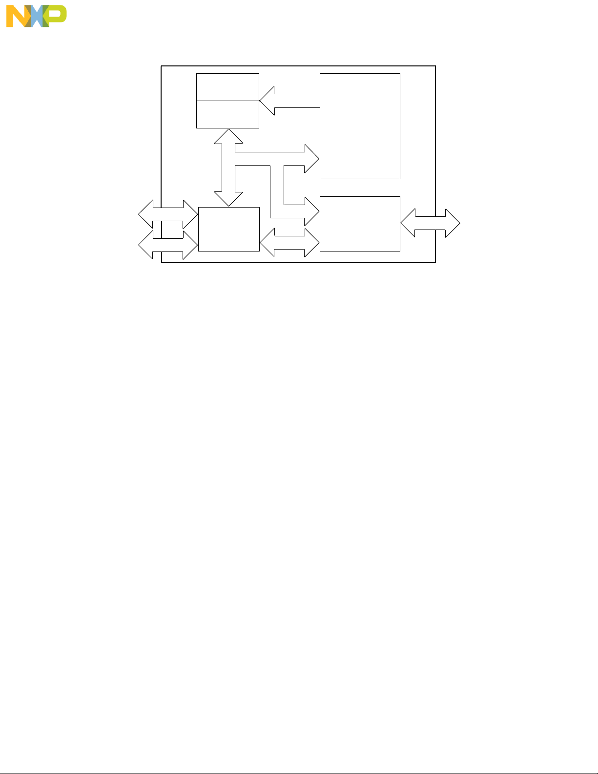
1.2 Block Diagram
A block diagram of the CPU32 is shown in Figure 1-2 . The functional elements operate concurrently. Essential synchronization of instruction execution and buss operation is maintained by the sequencer/control unit. The bus controller prefetches
instructions and operands. A three-stage pipeline is used to hold and decode instructions prior to execution. The execution unit maintains the program counter under sequencer control. The bus control contains a write-pending buffer that allows the
sequencer to continue execution of instructions after a request for a write cycle is
queued. See
nation of instruction execution.
SECTION 8 INSTRUCTION EXECUTION TIMING for a detailed expla-
MOTOROLA
1-6 REFERENCE MANUAL
For More Information On This Product,
Go to: www.freescale.com
OVERVIEW
CPU32
Page 21
Freescale Semiconductor, Inc.
SEQUENCER
CONTROL
UNIT
DATA BUS
ADDRESS BUS
nc...
I
16
EXECUTION
UNIT
32
INSTRUCTION
PIPELINE
AND
DECODE
BUS
CONTROL
BUS CONTROL
Figure 1-2 CPU32 Block Diagram
cale Semiconductor,
Frees
CPU32
REFERENCE MANUAL 1-7
For More Information On This Product,
Go to: www.freescale.com
OVERVIEW
MOTOROLA
Page 22

Freescale Semiconductor, Inc.
nc...
I
cale Semiconductor,
Frees
MOTOROLA
1-8 REFERENCE MANUAL
For More Information On This Product,
Go to: www.freescale.com
OVERVIEW
CPU32
Page 23

nc...
I
cale Semiconductor,
Frees
Freescale Semiconductor, Inc.
SECTION 2ARCHITECTURE SUMMARY
The CPU32 is upward source and object code compatible with the MC68000 and
MC68010. It is downward source and object code compatible with the MC68020. Within the M68000 Family, architectural differences are limited to the supervisory operating
state. User state programs can be executed unchanged on upward compatible devices.
The major CPU32 features are as follows:
• 32-Bit Internal Data Path and Arithmetic Hardware
• 32-Bit Address Bus Supported by 32-Bit Calculations
• Rich Instruction Set
• Eight 32-Bit General-Purpose Data Registers
• Seven 32-Bit General-Purpose Address Registers
• Separate User and Supervisor Stack Pointers
• Separate User and Supervisor State Address Spaces
• Separate Program and Data Address Spaces
• Many Data Types
• Flexible Addressing Modes
• Full Interrupt Processing
• Expansion Capability
2.1 Programming Model
The CPU32 programming model consists of two groups of registers that correspond
to the user and supervisor privilege levels. User programs can only use the registers
of the user model. The supervisor programming model, which supplements the user
programming model, is used by CPU32 system programmers who wish to protect sensitive operating system functions. The supervisor model is identical to that of
MC68010 and later processors.
The CPU32 has eight 32-bit data registers, seven 32-bit address registers, a 32-bit
program counter, separate 32-bit supervisor and user stack pointers, a 16-bit status
register, two alternate function code registers, and a 32-bit vector base register (see
Figure 2-1 and Figure 2-2 ).
CPU32
REFERENCE MANUAL 2-1
For More Information On This Product,
ARCHITECTURE SUMMARY
Go to: www.freescale.com
MOTOROLA
Page 24

Freescale Semiconductor, Inc.
31 16 15 8 7 0
31 16 15 0
nc...
I
31 16 15 0
31 0
D0
D1
D2
D3 DATA REGISTERS
D4
D5
D6
D7
A0
A1
A2
A3 ADDRESS REGISTERS
A4
A5
A6
A7 (USP) USER STACK POINTER
PC PROGRAM COUNTER
15 8 7 0
0 CCR CONDITION CODE REGISTER
cale Semiconductor,
Frees
Figure 2-1 User Programming Model
31 16 15 0
A7' (SSP) SUPERVISOR STACK
15 8 7 0
(CCR) SR STATUS REGISTER
31 0
PC VECTOR BASE REGISTER
31 3 2 0
SFC ALTERNATE FUNCTION
DFC CODE REGISTERS
POINTER
Figure 2-2 Supervisor Programming Model Supplement
2.2 Registers
Registers D7 to D0 are used as data registers for bit, byte (8-bit), word (16-bit), longword (32-bit), and quad-word (64-bit) operations. Registers A6 to A0 and the user and
supervisor stack pointers are address registers that may be used as software stack
pointers or base address registers. Register A7 (shown as A7 and A7' in
Figure 2-1 )
is a register designation that applies to the user stack pointer in the user privilege level
and to the supervisor stack pointer in the supervisor privilege level. In addition, address registers may be used for word and long-word operations. All of the 16 generalpurpose registers (D7 to D0, A7 to A0) may be used as index registers.
MOTOROLA
2-2 REFERENCE MANUAL
For More Information On This Product,
ARCHITECTURE SUMMARY
Go to: www.freescale.com
CPU32
Page 25
Freescale Semiconductor, Inc.
The program counter (PC) contains the address of the next instruction to be executed
by the CPU32. During instruction execution and exception processing, the processor
automatically increments the contents of the PC or places a new value in the PC, as
appropriate.
nc...
I
cale Semiconductor,
Frees
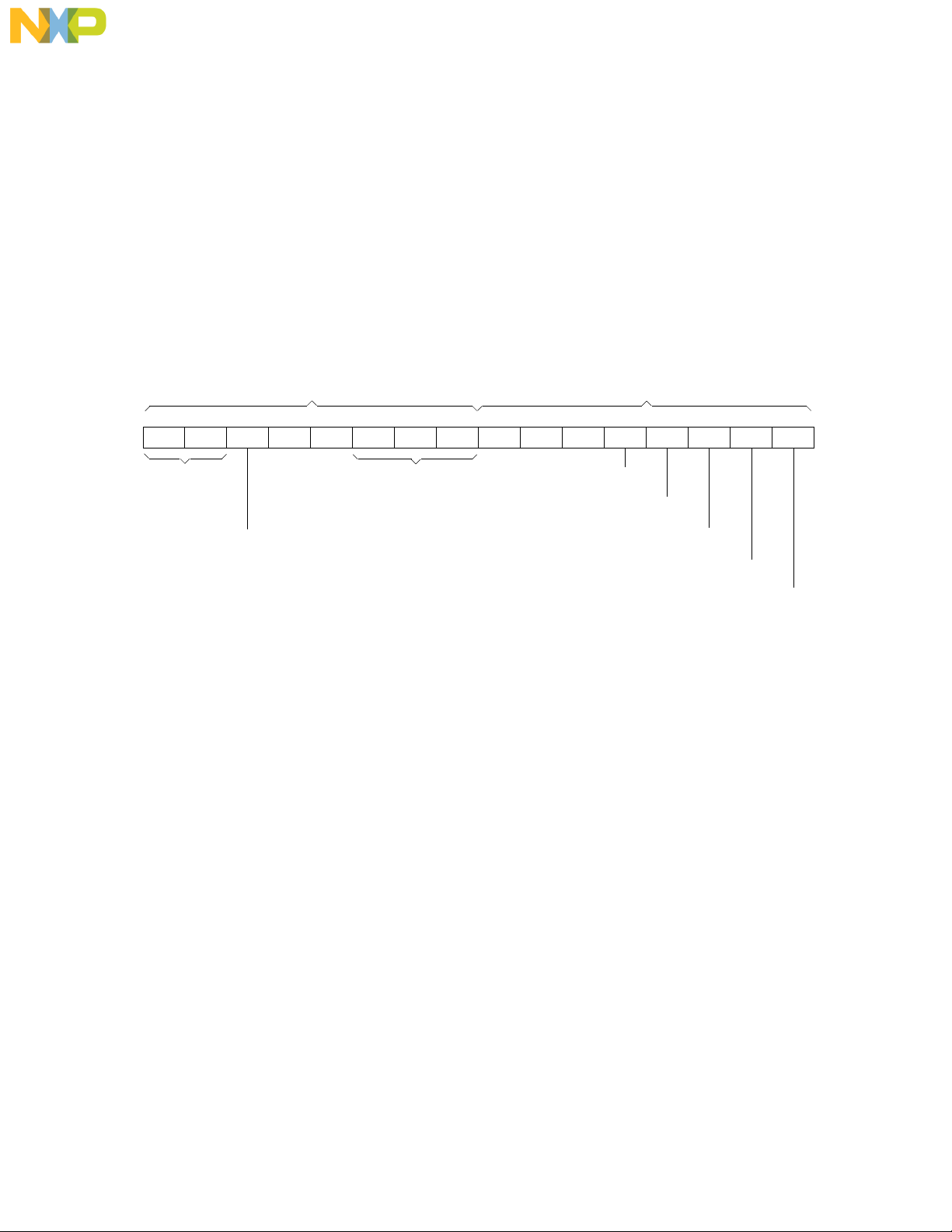
The status register (SR) (see
Figure 2-3 ) contains condition codes, an interrupt prior-
ity mask (three bits), and three control bits. Condition codes reflect the results of a previous operation. The codes are contained in the low byte, or condition code register of
the SR. The interrupt priority mask determines the level of priority an interrupt must
have in order to be acknowledged. The control bits determine trace mode and privilege
level. At user privilege level, only the condition code register is available. At supervisor
privilege level, software can access the full status register.
SYSTEM BYTE
15 14 13 12 11 10 9 8 7 6 5 4 3 2 1 0
T1 T0 S 0 0 I2 I1 I0 0 0 0 X N Z V C
TRACE
ENABLE
SUPERVISOR/USER
S TATE
INTERRUPT
PRIORITY MASK
USER BYTE
(CONDITION CODE REGISTER)
EXTEND
NEGATIVE
ZERO
OVERFLOW
CARRY
Figure 2-3 Status Register
The vector base register (VBR) contains the base address of the exception vector table in memory. The displacement of an exception vector is added to the value in this
register to access the vector table.
Alternate function code registers SFC and DFC contain 3-bit function codes. The
CPU32 generates a function code each time it accesses an address. Specific codes
are assigned to each type of access. The codes can be used to select eight dedicated
4G-byte address spaces. The MOVE instructions can use registers SFC and DFC to
specify the function code of a memory address.
2.3 Data Types
Six basic data types are supported:
1. Bits
2. Binary-Coded Decimal (BCD) Digits
3. Byte Integers (8 bits)
4. Word Integers (16 bits)
5. Long-Word Integers (32 bits)
6. Quad-Word Integers (64 bits)
CPU32
REFERENCE MANUAL 2-3
For More Information On This Product,
ARCHITECTURE SUMMARY
Go to: www.freescale.com
MOTOROLA
Page 26

Freescale Semiconductor, Inc.
2.3.1 Organization in Registers
The eight data registers can store data operands of 1, 8, 16, 32, and 64 bits and addresses of 16 or 32 bits. The seven address registers and the two stack pointers are
used for address operands of 16 or 32 bits. The PC is 32 bits wide.
2.3.1.1 Data Registers
Each data register is 32 bits wide. Byte operands occupy the low-order 8 bits, word
operands, the low-order 16 bits, and long-word operands, the entire 32 bits. When a
data register is used as either a source or destination operand, only the appropriate
low-order byte or word (in byte or word operations, respectively) is used or changed
— the remaining high-order portion is neither used nor changed. The least significant
bit (LSB) of a long-word integer is addressed as bit zero, and the most significant bit
(MSB) is addressed as bit 31. Figure 2-4 shows the organization of various types of
data in the data registers.
nc...
I
cale Semiconductor,
Frees
31 30 10
MSB LSB
BYTE
31 24 23 16 15 8 7 0
HIGH-ORDER BYTE MIDDLE HIGH BYTE MIDDLE LOW BYTE LOW-ORDER BYTE
WORD
31 16 15 0
HIGH-ORDER WORD LOW-ORDER WORD
LONG WORD
31 0
LONG WORD
QUAD WORD
63 62 32
MSB HIGH-ORDER LONG WORD
31 10
LOW-ORDER LONG WORD LSB
Figure 2-4 Data Organization in Data Registers
Quad-word data consists of two long words: for example, the product of 32-bit multiply
or the quotient of 32-bit divide operations (signed and unsigned). Quad words may be
organized in any two data registers without restrictions on order or pairing. There are
no explicit instructions for the management of this data type; however, the MOVEM
instruction can be used to move a quad word into or out of the registers.
MOTOROLA ARCHITECTURE SUMMARY CPU32
2-4 REFERENCE MANUAL
For More Information On This Product,
Go to: www.freescale.com
Page 27

Freescale Semiconductor, Inc.
BCD data represents decimal numbers in binary form. CPU32 BCD instructions use a
format in which a byte contains two digits — the four LSB contain the low digit, and the
four MSB contain the high digit. The ABCD, SBCD, and NBCD instructions operate on
two BCD digits packed into a single byte.
2.3.1.2 Address Registers
Each address register and stack pointer holds a 32-bit address. Address registers cannot be used for byte-sized operands. When an address register is used as a source
operand, either the low-order word or the entire long-word operand is used, depending
upon the operation size. When an address register is used as a destination operand,
the entire register is affected, regardless of operation size. If the source operand is a
word, it is first sign extended to 32 bits, and then used in the operation. Address registers can be used to support address computation. The instruction set includes instructions that add to, subtract from, compare, and move the contents of address
registers. Figure 2-5 shows the organization of addresses in address registers.
nc...
I
31 16 15 0
SIGN EXTENDED 16-BIT ADDRESS OPERAND
cale Semiconductor,
Frees
31 0
FULL 32-BIT ADDRESS OPERAND
Figure 2-5 Address Organization in Address Registers
2.3.1.3 Control Registers
The control registers contain control information for supervisor functions. The registers
vary in size. With the exception of the user portion of the SR (CCR), they are accessed
only by instructions at the supervisor privilege level.
The SR shown in Figure 2-3 is 16 bits wide. Only 11 bits of the SR are defined, and
all undefined values are reserved by Motorola for future definition. The undefined bits
are read as zeros and should be written as zeros for future compatibility. The lower
byte of the SR is the CCR. Operations to the CCR can be performed at the supervisor
or user privilege level. All operations to the SR and CCR are word-size operations. For
all CCR operations, the upper byte is read as all zeros and is ignored when written,
regardless of privilege level.
The alternate function code registers (SFC and DFC) are 32-bit registers with only bits
[2:0] implemented. These bits contain address space values (FC2 to FC0) for the read
or write operand of the MOVES instruction. The MOVEC instruction is used to transfer
values to and from the alternate function code registers. These are long-word transfers
— the upper 29 bits are read as zeros and are ignored when written.
CPU32 ARCHITECTURE SUMMARY MOTOROLA
REFERENCE MANUAL 2-5
For More Information On This Product,
Go to: www.freescale.com
Page 28

Freescale Semiconductor, Inc.
2.3.2 Organization in Memory
Memory is organized on a byte-addressable basis. An address corresponds to a highorder byte. For example, the address (N) of a long-word data item is the address of
the most significant byte of the high-order word. The address of the most significant
byte of the low-order word is (N + 2), and the address of the least significant byte of
the long word is (N + 3). The CPU32 requires data words and long words, as well as
instruction words to be aligned on word boundaries. Data misalignment is not supported. Figure 2-6 shows how operands and instructions are organized in memory. Note
that (N + X) is below (N) — that is, address value increases as one moves down the
page.
nc...
I
cale Semiconductor,
Frees
MOTOROLA ARCHITECTURE SUMMARY CPU32
2-6 REFERENCE MANUAL
For More Information On This Product,
Go to: www.freescale.com
Page 29
Freescale Semiconductor, Inc.
15 8 7 0
MSB BYTE 0 LSB BYTE 1
BYTE 2 BYTE 3
15 0
MSB
nc...
I
15 0
MSB
LONG WORD 0
BIT DATA
1 BYTE = 8 BITS
76543210
BYTE DATA
(8 BITS)
WORD DATA / INSTRUCTION
(16 BITS)
WORD 0 LSB
WORD 1
WORD 2
LONG WORD DATA / INSTRUCTION
(32 BITS)
HIGH ORDER
LOW ORDER
LSB
cale Semiconductor,
Frees
LONG WORD 1
LONG WORD 2
ADDRESS
15
MSB
MSB = Most Significant Bit
LSB = Least Significant Bit
15 12 11 8 7 4 3 0
MSD = Most Significant Digit
LSD = Least Significant Digit
BCD 4
ADDRESS 0
ADDRESS 1
ADDRESS 2
MSDBCD 0
BCD 1
BCD 5
(32 BITS)
HIGH ORDER
LOW ORDER
DECIMAL DATA
2 BCD DIGITS = 1 BYTE
LSD
BCD 2
BCD 6
LSB
BCD 3
BCD 7
0
Figure 2-6 Memory Operand Addressing
CPU32 ARCHITECTURE SUMMARY MOTOROLA
REFERENCE MANUAL 2-7
For More Information On This Product,
Go to: www.freescale.com
Page 30

Freescale Semiconductor, Inc.
nc...
I
cale Semiconductor,
Frees
MOTOROLA ARCHITECTURE SUMMARY CPU32
2-8 REFERENCE MANUAL
For More Information On This Product,
Go to: www.freescale.com
Page 31

Freescale Semiconductor, Inc.
SECTION 3 DATA ORGANIZATION AND ADDRESSING CAPABILITIES
The addressing mode of an instruction can specify the value of an operand (an immediate operand), a register that contains the operand (register direct addressing mode),
or how the effective address of an operand in memory is derived. An assembler syntax
has been defined for each addressing mode.
Figure 3-1 shows the general format of the single-effective-address instruction operation word. The effective address field specifies the addressing mode for an operand
that can use one of the numerous defined modes. The designation is composed of two
3-bit fields, the mode field and the register field. The value in the mode field selects a
mode or a set of modes. The register field specifies a register for the mode or a submode for modes that do not use registers.
nc...
I
15 14 13 12 11 10 9 8 7 6 5 4 3 2 1 0
X X X X X X X X X X EFFECTIVE ADDRESS
cale Semiconductor,
Frees
MODE REGISTER
Figure 3-1 Single-Effective-Address Instruction Operation Word
Many instructions imply the addressing mode for only one of the operands. The formats of these instructions include appropriate fields for operands that use only a single
addressing mode.
Additional information may be needed to specify an operand address. This information
is contained in an additional word or words called the effective address extension, and
is considered part of an instruction. Address extension formats are discussed in 3.4.4
Effective Address Encoding Summary.
When an addressing mode uses a register, the register is specified by the register field
of the operation word. Other fields within the instruction specify whether the selected
register is an address or data register and how the register is to be used.
3.1 Program and Data References
An M68000 Family processor makes two classes of memory references, each of
which has a complete, separate logical address space.
References to opcodes and extension words are program space references.
Operand reads and writes are primarily data space references. Operand reads are
from data space in all but two cases — immediate operands embedded in the instruction stream and operands addressed relative to the current program counter are program space references. All operand writes are to data space.
CPU32 DATA ORGANIZATION AND ADDRESSING CAPABILITIES MOTOROLA
REFERENCE MANUAL 3-1
For More Information On This Product,
Go to: www.freescale.com
Page 32

nc...
I
cale Semiconductor,
Frees
Freescale Semiconductor, Inc.
3.2 Notation Conventions
EA — Effective address
An — Address register n
Example: A3 is address register 3
Dn — Data register n
Example: D5 is data register 5
Rn — Any register, data or address
Xn.SIZE*SCALE —
Index register n (data or address),
Index size (W for word, L for long word),
Scale factor (1, 2, 4, or 8 for byte, word, long-word or quad-word scaling)
PC — Program counter
SR — Status register
SP — Stack pointer
CCR — Condition code register
USP — User stack pointer
SSP — Supervisor stack pointer
dn — Displacement value, n bits wide
bd — Base displacement
L — Long-word size
W — Word size
B — Byte size
(An) — Identifies an indirect address in a register
3.3 Implicit Reference
Some instructions make implicit reference to the program counter, the system stack
pointer, the user stack pointer, the supervisor stack pointer, or the status register. The
following table shows the instructions and the registers involved:
Instruction Implicit Registers
ANDI to CCR SR
ANDI to SR SR
BRA PC
BSR PC, SP
CHK (exception) PC, SP
CHK2 (exception) SSP, SR
DBcc PC
DIVS (exception) SSP, SR
DIVU (exception) SSP, SR
EORI to CCR SR
EORI to SR SR
JMP PC
JSR PC, SP
LINK SP
LPSTOP SR
MOVE CCR SR
MOVE SR SR
MOVE USP USP
MOTOROLA DATA ORGANIZATION AND ADDRESSING CAPABILITIES CPU32
3-2 REFERENCE MANUAL
For More Information On This Product,
Go to: www.freescale.com
Page 33

Freescale Semiconductor, Inc.
ORI to CCR SR
ORI to SR SR
PEA SP
RTD PC, SP
RTE PS, SP, SR
RTR PC, SP, SR
RTS PC, SP
STOP SR
TRAP (exception) SSP, SR
TRAPV (exception) SSP, SR
UNLK SP
Instruction Implicit Registers
3.4 Effective Address
Most instructions specify the location of an operand by a field in the operation word
called an effective address field or an effective address (〈EA〉). An EA is composed of
nc...
I
two 3-bit subfields: mode specification field and register specification field. Each of the
address modes is selected by a particular value in the mode specification subfield of
the EA. The EA field may require further information to fully specify the operand. This
information, called the EA extension, is in a following word or words and is considered
part of the instruction (see 3.1 Program and Data References).
cale Semiconductor,
Frees
3.4.1 Register Direct Mode
These EA modes specify that the operand is in one of the 16 multifunction registers.
3.4.1.1 Data Register Direct
In the data register direct mode, the operand is in the data register specified by the EA
register field.
GENERATION:
ASSEMBLER SYNTAX:
MODE:
REGISTER:
DATA REGISTER:
NUMBER OF EXTENSION WORDS:
EA = Dn
Dn
000
n
Dn
0
OPERAND
3.4.1.2 Address Register Direct
In the address register direct mode, the operand is in the address register specified by
the EA register field.
GENERATION:
ASSEMBLER SYNTAX:
MODE:
REGISTER:
DATA REGISTER:
NUMBER OF EXTENSION WORDS:
EA = An
An
001
n
An
0
OPERAND
031
031
CPU32 DATA ORGANIZATION AND ADDRESSING CAPABILITIES MOTOROLA
REFERENCE MANUAL 3-3
For More Information On This Product,
Go to: www.freescale.com
Page 34

Freescale Semiconductor, Inc.
3.4.2 Memory Addressing Modes
These EA modes specify the address of the memory operand.
3.4.2.1 Address Register Indirect
In the address register indirect mode, the operand is in memory, and the address of
the operand is in the address register specified by the register field.
GENERATION:
ASSEMBLER SYNTAX:
MODE:
REGISTER:
ADDRESS REGISTER:
MEMORY ADDRESS:
NUMBER OF EXTENSION WORDS: 0
nc...
I
3.4.2.2 Address Register Indirect With Postincrement
EA = (An)
(An)
010
n
An
031
MEMORY ADDRESS
031
OPERAND
In the address register indirect with postincrement mode, the operand is in memory,
and the address of the operand is in the address register specified by the register field.
After the operand address is used, it is incremented by one, two, or four, depending
on the size of the operand: byte, word, or long word. If the address register is the stack
pointer and the operand size is byte, the address is incremented by two rather than
one to keep the stack pointer aligned to a word boundary.
GENERATION:
ASSEMBLER SYNTAX:
MODE:
REGISTER:
ADDRESS REGISTER:
cale Semiconductor,
OPERAND LENGTH ( 1, 2, OR 4):
MEMORY ADDRESS:
NUMBER OF EXTENSION WORDS: 0
EA = (An)
An = An + SIZE
(An) +
011
n
An
031
MEMORY ADDRESS
+
031
OPERAND
Frees
3.4.2.3 Address Register Indirect With Predecrement
In the address register indirect with predecrement mode, the operand is in memory,
and the address of the operand is in the address register specified by the register field.
Before the operand address is used, it is decremented by one, two, or four, depending
on the operand size: byte, word, or long word. If the address register is the stack pointer and the operand size is byte, the address is decremented by two rather than one to
keep the stack pointer aligned to a word boundary.
MOTOROLA DATA ORGANIZATION AND ADDRESSING CAPABILITIES CPU32
3-4 REFERENCE MANUAL
For More Information On This Product,
Go to: www.freescale.com
Page 35

Freescale Semiconductor, Inc.
nc...
I
cale Semiconductor,
Frees
GENERATION:
ASSEMBLER SYNTAX:
MODE:
REGISTER:
ADDRESS REGISTER:
OPERAND LENGTH (1, 2, OR 4):
MEMORY ADDRESS:
NUMBER OF EXTENSION WORDS: 0
An = An SIZE
EA = (An)
(An)
100
n
An
MEMORY ADDRESS
OPERAND
3.4.2.4 Address Register Indirect With Displacement
In the address register indirect with displacement mode, the operand is in memory.
The address of the operand is the sum of the address in the address register plus the
sign-extended 16-bit displacement integer in the extension word. Displacements are
always sign extended to 32 bits before being used in EA calculations.
GENERATION:
ASSEMBLER SYNTAX:
MODE:
REGISTER:
ADDRESS REGISTER:
31 15
DISPLACEMENT:
MEMORY ADDRESS:
NUMBER OF EXTENSION WORDS: 1
SIGN EXTENDED
EA = (An) + d
(d An)
16,
101
n
An
16
MEMORY ADDRESS
0
INTEGER
31
+
OPERAND
3.4.2.5 Address Register Indirect With Index (8-Bit Displacement)
This mode requires one extension word that contains the index register indicator and
an 8-bit displacement. The index register indicator includes size and scale information.
In this mode, the operand is in memory. The address of the operand is the sum of the
contents of the address register, the sign-extended displacement value in the low-order eight bits of the extension word, and the sign-extended contents of the index register (possibly scaled). The user must specify displacement, address register, and
index register.
031
031
031
0
This address mode can have either of two different formats of extension. The brief format (8-bit displacement) requires one word of extension and provides fast indexed addressing. The full format (16 and 32-bit displacement) provides optional displacement
size. Both forms use an index operand.
For brief format addressing, the address of the operand is the sum of the address in
the address register, the sign-extended displacement integer in the low-order eight
bits of the extension word, and the index operand. The reference is classed as a data
reference, except for the JMP and JSR instructions. The index operand is specified
“Ri.sz*scl”.
CPU32 DATA ORGANIZATION AND ADDRESSING CAPABILITIES MOTOROLA
REFERENCE MANUAL 3-5
For More Information On This Product,
Go to: www.freescale.com
Page 36

Freescale Semiconductor, Inc.
GENERATION:
ASSEMBLER SYNTAX:
MODE:
REGISTER:
ADDRESS REGISTER:
DISPLACEMENT:
INDEX REGISTER:
SCALE:
MEMORY ADDRESS:
NUMBER OF EXTENSION WORDS: 1
EA = (An) + (Xn*SCALE) + d
,
(d An. SIZE*SCALE)
8
110
n
An
SIGN-EXTENDED VALUE
8
31
7
INTEGERSIGN EXTENDED
SCALE VALUE
MEMORY ADDRESS
031
031
X
OPERAND
0
+
+
031
“Ri” specifies a general data or address register used as an index register. The index
operand is derived from the index register. The index register is a data register if bit
nc...
I
[15] = 0 in the first extension word and an address register if bit [15] = 1. The index
register number is given by extension word bits [14:12].
Index size is referred to as “sz”. It may be either “W” or “L”. Index size is given by bit
[11] of the extension word. If bit [11] = 0, the index value is the sign-extended low-order
word integer of the index register (W). If bit [11] = 1, the index value is the long integer
in the index register (L).
The term “scl” refers to index scale selection and may be 1, 2, 4, or 8. The index value
is scaled according to bits [10:9]. Codes 00, 01, 10, or 11 select index scaling of 1, 2,
4, or 8, respectively.
3.4.2.6 Address Register Indirect With Index (Base Displacement)
The full format indexed addressing mode requires an index register indicator and an
optional 16- or 32-bit sign-extended base displacement. The index register indicator
cale Semiconductor,
includes size and scale information. In this mode, the operand is in memory. The address of the operand is the sum of the contents of the address register, the scaled contents of the sign-extended index register, and the base displacement.
Frees
GENERATION:
ASSEMBLER SYNTAX:
MODE:
REGISTER:
ADDRESS REGISTER:
BASE DISPLACEMENT:
INDEX REGISTER:
SCALE:
MEMORY ADDRESS:
NUMBER OF EXTENSION WORDS: 1, 2, OR 3
MOTOROLA DATA ORGANIZATION AND ADDRESSING CAPABILITIES CPU32
3-6 REFERENCE MANUAL
For More Information On This Product,
EA = (An) + (Xn*SCALE) + bd
(bd, An, Xn. SIZE*SCALE)
110
n
An
SIGN-EXTENDED VALUE
SIGN-EXTENDED VALUE
31
SCALE VALUE
Go to: www.freescale.com
MEMORY ADDRESS
031
031
X
OPERAND
0
+
+
031
Page 37

Freescale Semiconductor, Inc.
3.4.3 Special Addressing Modes
These special addressing modes do not use the register field to specify a register number but rather to specify a submode.
3.4.3.1 Program Counter Indirect With Displacement
In this mode, the operand is in memory. The address of the operand is the sum of the
address in the program counter and the sign-extended 16-bit displacement integer in
the extension word. The value in the program counter is the address of the extension
word. The reference is a program space reference and is only allowed for read accesses.
nc...
I
cale Semiconductor,
Frees
GENERATION:
ASSEMBLER SYNTAX:
MODE:
REGISTER:
PROGRAM COUNTER:
31 15
DISPLACEMENT:
MEMORY ADDRESS:
NUMBER OF EXTENSION WORDS: 1
SIGN EXTENDED
EA = (PC) + d
(d , PC)
16
111
010
16
ADDRESS OF EXTENSION WORD
0
INTEGER
31
+
OPERAND
3.4.3.2 Program Counter Indirect with Index (8-Bit Displacement)
This mode is similar to the address register indirect with index (8-bit displacement)
mode described in 3.4.2.5 Address Register Indirect With Index (8-Bit Displace-
ment), but the program counter is used as the base register.
GENERATION:
ASSEMBLER SYNTAX:
MODE:
REGISTER:
PROGRAM COUNTER:
DISPLACEMENT:
INDEX REGISTER:
SCALE:
EA = (PC) + (Xn) + d
(d , PC, Xn. SIZE*SCALE)
8
111
011
SIGN-EXTENDED VALUE
8
31
7
INTEGERSIGN EXTENDED
SCALE VALUE
ADDRESS OF EXTENSION WORD
031
031
X
+
+
031
0
0
MEMORY ADDRESS:
NUMBER OF EXTENSION WORDS: 1
OPERAND
031
The operand is in memory. The address of the operand is the sum of the address in
the program counter, the sign-extended displacement integer in the lower eight bits of
the extension word, and the sized, scaled, and sign-extended index operand. The value in the program counter is the address of the extension word. This reference is a
program space reference and is only allowed for reads. The user must include the displacement, the program counter, and the index register when specifying this addressing mode.
CPU32 DATA ORGANIZATION AND ADDRESSING CAPABILITIES MOTOROLA
REFERENCE MANUAL 3-7
For More Information On This Product,
Go to: www.freescale.com
Page 38

Freescale Semiconductor, Inc.
3.4.3.3 Program Counter Indirect with Index (Base Displacement)
This mode is similar to the address register indirect with index (base displacement)
mode described in 3.4.2.6 Address Register Indirect With Index (Base Displace-
ment), but the program counter is used as the base register. It requires an index register indicator and an optional 16- or 32-bit sign-extended base displacement.
The operand is in memory. The address of the operand is the sum of the contents of
the program counter, the scaled contents of the sign-extended index register, and the
base displacement. The value of the program counter is the address of the first extension word. The reference is a program space reference and is only allowed for read
accesses.
In this mode, the program counter, the index register, and the displacement are all optional. However, the user must supply the assembler notation “ZPC” (zero value is taken for the program counter) to indicate that the program counter is not used. This
scheme allows the user to access the program space without using the program
nc...
I
counter in calculating the EA. The user can access the program space with a data register indirect access by placing ZPC in the instruction and specifying a data register
(Dn) as the index register.
cale Semiconductor,
Frees
GENERATION:
ASSEMBLER SYNTAX:
MODE:
REGISTER:
PROGRAM COUNTER:
BASE DISPLACEMENT:
INDEX REGISTER:
SCALE:
MEMORY ADDRESS:
NUMBER OF EXTENSION WORDS: 1, 2, OR 3
EA = (PC) + (Xn) + bd
(bd, PC, Xn. SIZE*SCALE)
111
011
SIGN-EXTENDED VALUE
SIGN-EXTENDED VALUE
31
SCALE VALUE
ADDRESS OF EXTENSION WORD
031
031
X
OPERAND
+
+
3.4.3.4 Absolute Short Address
In this addressing mode, the operand is in memory, and the address of the operand is
in the extension word. The 16-bit address is sign extended to 32 bits before it is used.
GENERATION:
ASSEMBLER SYNTAX:
MODE:
REGISTER:
EXTENSION WORD:
EA GIVEN
(xxx).W
111
000
15
MEMORY ADDRESSSIGN EXTENDED
0
031
031
MEMORY ADDRESS:
NUMBER OF EXTENSION WORDS: 1
MOTOROLA DATA ORGANIZATION AND ADDRESSING CAPABILITIES CPU32
3-8 REFERENCE MANUAL
For More Information On This Product,
Go to: www.freescale.com
OPERAND
031
Page 39

Freescale Semiconductor, Inc.
3.4.3.5 Absolute Long Address
In this mode, the operand is in memory, and the address of the operand occupies the
two extension words following the instruction word in memory. The first extension word
contains the high-order part of the address; the low-order part of the address is the
second extension word.
nc...
I
cale Semiconductor,
Frees
GENERATION:
ASSEMBLER SYNTAX:
MODE:
REGISTER:
FIRST EXTENSION WORD:
SECOND EXTENSION WORD:
MEMORY ADDRESS:
NUMBER OF EXTENSION WORDS: 2
EA GIVEN
(xxx).L
111
001
15
ADDRESS HIGH
0
15
CONCATENATION
OPERAND
3.4.3.6 Immediate Data
In this addressing mode, the operand is in one or two extension words:
Byte Operation
The operand is in the low-order byte of the extension word.
Word Operation
The operand is in the extension word.
Long-Word Operation
The high-order 16 bits of the operand are in the first extension word; the low-order
16 bits are in the second extension word.
GENERATION:
ASSEMBLER SYNTAX:
MODE:
REGISTER:
NUMBER OF EXTENSION WORDS:
OPERAND GIVEN
#XXX
111
100
1 OR 2
ADDRESS LOW
0
0
031
031
3.4.4 Effective Address Encoding Summary
Most addressing modes use one of the three formats shown in Figure 3-2. The single
EA instruction is in the format of the instruction word. The mode field of this word selects the addressing mode. The register field contains the general register number or
a value that selects the addressing mode when the mode field contains “111”.
Some indexed or indirect modes use the instruction word followed by the brief format
extension word. Other indexed or indirect modes consist of the instruction word and
the full format of extension words. The longest instruction for the CPU32 contains six
extension words. It is a MOVE instruction with full format extension words for both
source and destination EA and a 32-bit base displacement for both addresses.
CPU32 DATA ORGANIZATION AND ADDRESSING CAPABILITIES MOTOROLA
REFERENCE MANUAL 3-9
For More Information On This Product,
Go to: www.freescale.com
Page 40

Freescale Semiconductor, Inc.
15 14 13 12 11 10 9 8 7 6 5 4 3 2 1 0
X X X X X X X X X X
15 14 12 11 10 9 8 7 0
D/A REGISTER W/ L SCALE 0 DISPLACEMENT
15 14 12 11 10 9 8 7 6 5 4 3 2 0
D/A REGISTER W/ L SCALE 1 BS IS BD SIZE 0 I/IS
SINGLE EA INSTRUCTION FORMAT
EFFECTIVE ADDRESS
MODE REGISTER
BRIEF FORMAT EXTENSION WORD
FULL FORMAT EXTENSION WORD(S)
BASE DISPLACEMENT (0, 1, OR 2 WORDS)
nc...
I
cale Semiconductor,
Frees
Field Definition Field Definition
Instruction BS Base Register Suppress
Register General Register Number 0 = Base Register Added
Extension 1 = Base Register Suppressed
Register Index Register Number IS Index Suppress
D/A Index Register Type 0 = Evaluate and Add Index Operand
0 = Dn 1 = Suppress Index Operand
1 = An BD SIZE Base Displacement Size
W/L Word/Long Word Index Size 00 = Reserved
0 = Sign-Extended Word 01 = Null Displacement
1 = Long Word 10 = Word Displacement
Scale Scale Factor 11 = Long-Word Displacement
00 = 1 I/IS * Index/Indirect Selection
01 = 2 Indirect and Indexing Operand
10 = 4 Determined in Conjunction with Bit 6,
11 = 8 Index Suppress
*Memory indirect addressing will cause illegal instruction trap; must be = 000 if IS = 1
Figure 3-2 Effective Address Specification Formats
EA modes can be classified as follows:
Data A data addressing EA mode refers to data operands.
Memory A memory addressing EA mode refers to memory operands.
Alterable An alterable addressing EA mode refers to writable operands.
Control A control addressing EA mode refers to unsized memory operands.
Categories are sometimes combined, forming new, more restrictive, categories. Two
examples are alterable memory or alterable data. The former refers to addressing
modes that are both alterable and memory addresses; the latter refers to addressing
modes that are both alterable and data addresses. Table 3-1 shows categories to
which each of the EA modes belong.
MOTOROLA DATA ORGANIZATION AND ADDRESSING CAPABILITIES CPU32
3-10 REFERENCE MANUAL
For More Information On This Product,
Go to: www.freescale.com
Page 41

nc...
I
cale Semiconductor,
Frees
Freescale Semiconductor, Inc.
3.5 Programming View of Addressing Modes
Extensions to indexed addressing modes, indirection, and full 32-bit displacements
provide additional programming capabilities for the CPU32. The following paragraphs
describe addressing techniques and summarize addressing modes from a programming point of view.
Table 3-1 Effective Addressing Mode Categories
Addressing Mode Code Register Data Memory Control Alterable Syntax
Data Register Direct 000 reg. no. X — — X Dn
Address Register Direct 001 reg. no. — — — X An
Address Register Indirect 010 reg.no. X X X X (An)
Address Register Indirect
with Postincrement
Address Register Indirect
with Predecrement
Address Register Indirect
with Displacement
Address Register Indirect
with Index
(8-Bit Displacement)
Address Register Indirect
with Index
(Base Displacement)
Absolute Short 111 000 X X X X (xxx).W
Absolute Long 111 001 X X X X (xxx).L
Program Counter Indirect
with Displacement
Program Counter Indirect
with Index
(8-Bit Displacement)
Program Counter Indirect
with Index
(Base Displacement)
Immediate 111 100 X X — — #(data)
011 reg. no. X X — X (An) +
100 reg. no. X X — X – (An)
101 reg.no. X X X X (d
110 reg. no. X X X X (d
110 reg. no. X X X X (bd, An, Xn)
111 010 X — X X (d
111 011 X — X X (d
An)
16,
, An, Xn)
8
, PC)
16
, PC, Xn)
8
3.5.1 Addressing Capabilities
In the CPU32, setting the base register suppress (BS) bit in the full format extension
word (see Figure 3-2) suppresses use of the base address register in calculating the
EA, allowing any index register to be used in place of the base register. Because any
data register can be an index register, this provides a data register indirect form (Dn).
This mode could also be called register indirect (Rn) because either a data register or
an address register can be used to address memory — an extension of M68000 Family addressing capability.
The ability to specify the size and scale of an index register (Xn.SIZE ∗ SCALE) in
these modes provides additional addressing flexibility. When using the SIZE parameter, either the entire contents of the index register can be used, or the least significant
word can be sign extended to provide a 32-bit index value (refer to Figure 3-3).
CPU32 DATA ORGANIZATION AND ADDRESSING CAPABILITIES MOTOROLA
REFERENCE MANUAL 3-11
For More Information On This Product,
Go to: www.freescale.com
Page 42

Freescale Semiconductor, Inc.
31
DLW
USED IN ADDRESS CALCULATION
16
15 0
D1
Figure 3-3 Using SIZE in the Index Selection
For the CPU32, the register indirect modes can be extended further. Because displacements can be 32 bits wide, they can represent absolute addresses or the results
of expressions that contain absolute addresses. This scheme allows the general register indirect form to be (bd, Rn) or (bd, An, Rn) when the base register is not suppressed. Thus, an absolute address can be directly indexed by one or two registers
(refer to Figure 3-4).
nc...
I
Setting the index register suppress bit (IS) in the full format extension word suppresses
the index operand. The indirect suppressed index register mode uses the contents of
register An as an index to the pointer located at the address specified by the displacement. The actual data item is at the address in the selected pointer.
An optional scaling function supports direct array subscripting. An index register can
be left shifted by zero, one, two, or three bits before use in an EA calculation, to scale
for an array of elements of corresponding size. This is much more efficient than using
an arithmetic value in one of the general-purpose registers to multiply the index register by one, two, four, or eight.
SYNTAX: (bd,An,Rn)
bd
cale Semiconductor,
An
Rn
Frees
Figure 3-4 Using Absolute Address with Indexes
Scaling does not add to the EA calculation time. However, when combined with the
appropriate derived modes, scaling produces additional capabilities. Arrayed structures can be addressed absolutely and then subscripted; for example, (bd, Rn ∗
SCALE). Optionally, an address register that contains a dynamic displacement can be
MOTOROLA DATA ORGANIZATION AND ADDRESSING CAPABILITIES CPU32
3-12 REFERENCE MANUAL
For More Information On This Product,
Go to: www.freescale.com
Page 43

Freescale Semiconductor, Inc.
included in the address calculation (bd, An, Rn ∗ SCALE). Another variation that can
be derived is (An, Rn ∗ SCALE). In the first case, the array address is the sum of the
contents of a register and a displacement (see Figure 3-5). In the second example,
An contains the address of an array and Rn contains a subscript.
SYNTAX: MOVE.W (A5,A6.L*SCALE),(A7)
WHERE:
A5 = ADDRESS OF ARRAY STRUCTURE
A6 = INDEX NUMBER OF ARRAY ITEM
A7 = STACK POINTER
SIMPLE ARRAY
(SCALE = 1)
7
A6 = 1
2
nc...
I
cale Semiconductor,
3
4
RECORD OF 2 WORDS
(SCALE = 4)
15 0
A6 = 1
2
0
A6 = 1
2
A6 = 1
RECORD OF 1 WORD
(SCALE = 2)
15
RECORD OF 4 WORDS
(SCALE = 8)
15
0
0
Frees
2
NOTE: Regardless of array structure,
software increments index to
point to next record.
Figure 3-5 Addressing Array Items
CPU32 DATA ORGANIZATION AND ADDRESSING CAPABILITIES MOTOROLA
REFERENCE MANUAL 3-13
For More Information On This Product,
Go to: www.freescale.com
Page 44

Freescale Semiconductor, Inc.
3.5.2 General Addressing Mode Summary
The addressing modes described in the previous paragraphs are derived from specific
combinations of options in the indexing mode or a selection of two alternate addressing modes. For example, the addressing mode called register indirect (Rn) assembles
as address register indirect if the register is an address register. If Rn is a data register,
the assembler uses address register indirect with index mode, with a data register as
the indirect register, and suppresses the address register by setting the base suppress
bit in the EA specification.
Assigning an address register as Rn provides higher performance than using a data
register as Rn. Another case is (bd, An), which selects an addressing mode based on
the size of the displacement. If the displacement is 16 bits or less, the address register
indirect with displacement mode (d
quired, the address register indirect with index (bd, An, Xn) is used with the index register suppressed.
, An) is used. When a 32-bit displacement is re-
16
nc...
I
cale Semiconductor,
Frees
It is useful to examine the derived addressing modes available to a programmer (without regard to the CPU32 EA mode actually encoded) because the programmer need
not be concerned about these decisions. The assembler can choose the more efficient
addressing mode to encode.
3.6 M68000 Family Addressing Capability
Programs can be easily transported from one member of the M68000 Family to another. The user object code of earlier members of the family is upwardly compatible with
later members and can be executed without change. The address extension word(s)
are encoded with information that allows the CPU32 to distinguish new additions to the
basic M68000 Family architecture.
Earlier microprocessors have no knowledge of extension word formats implemented
in later processors, and, while they do detect illegal instructions, they do not decode
invalid encodings of the extension words as exceptions.
Address extension words for the early MC68000, MC68008, MC68010, and MC68020
microprocessors are shown in Figure 3-6.
MOTOROLA DATA ORGANIZATION AND ADDRESSING CAPABILITIES CPU32
3-14 REFERENCE MANUAL
For More Information On This Product,
Go to: www.freescale.com
Page 45

Freescale Semiconductor, Inc.
MC6800/MC68008/MC68010 ADDRESS EXTENSION WORD
15 14 12 11 10 9 8 7 0
D/A REGISTER W/ L 0 0 0 DISPLACEMENT INTEGER
D/A: 0 = Data Register Select
1 = Address Register Select
W/L 0 = Word-Sized Operation
1 = Long-Word-Sized Operation
15 14 12 11 10 9 8 7 0
D/A REGISTER W/ L SCALE 0 DISPLACEMENT INTEGER
D/A: 0 = Data Register Select
1 = Address Register Select
W/L 0 = Word-Sized Operation
1 = Long-Word-Sized Operation
SCALE: 00 = Scale Factor 1 (Compatible with MC68000)
01 = Scale Factor 2 (Extension to MC68000)
10 = Scale Factor 4 (Extension to MC68000)
nc...
I
11 = Scale Factor 8 (Extension to MC68000)
CPU32/MC68020 EXTENSION WORD
Figure 3-6 M68000 Family Address Extension Words
cale Semiconductor,
Frees
The encoding for SCALE used by the CPU32 and the MC68020 is a compatible extension of the M68000 architecture. A value of zero for SCALE is the same encoding
for both extension words; thus, software that uses this encoding is both upward and
downward compatible across all processors in the product line. However, the other
values of SCALE are not found in both extension formats; therefore, while software
can be easily migrated in an upward compatible direction, only nonscaled addressing
is supported in a downward fashion. If the MC68000 were to execute an instruction
that encoded a scaling factor, the scaling factor would be ignored and would not access the desired memory address.
3.7 Other Data Structures
In addition to supporting the array data structure with the index addressing mode,
M68000 processors also support stack and queue data structures with the address
register indirect postincrement and predecrement addressing modes. A stack is a lastin-first-out (LIFO) list; a queue is a first-in-first-out (FIFO) list. When data is added to a
stack or queue, it is pushed onto the structure; when it is removed, it is “popped”, or
pulled, from the structure. The system stack is used implicitly by many instructions;
user stacks and queues may be created and maintained through use of addressing
modes.
3.7.1 System Stack
Address register 7 (A7) is the system stack pointer (SP). The SP is either the supervisor stack pointer (SSP) or the user stack pointer (USP), depending on the state of the
S bit in the status register. If the S bit indicates the supervisor state, the SSP is the SP,
and the USP cannot be referenced as an address register. If the S bit indicates the
user state, the USP is the active SP, and the SSP cannot be referenced. Each system
CPU32 DATA ORGANIZATION AND ADDRESSING CAPABILITIES MOTOROLA
REFERENCE MANUAL 3-15
For More Information On This Product,
Go to: www.freescale.com
Page 46

Freescale Semiconductor, Inc.
stack fills from high memory to low memory. The address mode –(SP) creates a new
item on the active system stack, and the address mode (SP)+ deletes an item from the
active system stack.
The program counter is saved on the active system stack on subroutine calls and is
restored from the active system stack on returns. On the other hand, both the program
counter and the status register are saved on the supervisor stack during the processing of traps and interrupts. Thus, the correct execution of the supervisor state code is
not dependent on the behavior of user code, and user programs may use the USP arbitrarily.
To keep data on the system stack aligned properly, data entry on the stack is restricted
so that data is always put in the stack on a word boundary. Thus, byte data is pushed
on or pulled from the system stack in the high-order half of the word; the low-order half
is unchanged.
nc...
I
cale Semiconductor,
Frees
3.7.2 User Stacks
The user can implement stacks with the address register indirect with postincrement
and predecrement addressing modes. With address register An (n = 0 to 6), the user
can implement a stack that is filled either from high to low memory or from low to high
memory. Important considerations are as follows:
• Use the predecrement mode to decrement the register before its contents are
used as the pointer to the stack.
• Use the postincrement mode to increment the register after its contents are used
as the pointer to the stack.
• Maintain the SP correctly when byte, word, and long-word items are mixed in
these stacks.
To implement stack growth from high to low memory, use –(An) to push data on the
stack, (An)+ to pull data from the stack.
For this type of stack, after either a push or a pull operation, register An points to the
top item on the stack. This scheme is illustrated as follows:
LOW MEMORY
(FREE)
An
TOP OF STACK
BOTTOM OF STACK
HIGH MEMORY
To implement stack growth from low to high memory, use (An) + to push data on the
stack, –(An) to pull data from the stack.
In this case, after either a push or pull operation, register An points to the next available space on the stack. This scheme is illustrated as follows:
MOTOROLA DATA ORGANIZATION AND ADDRESSING CAPABILITIES CPU32
3-16 REFERENCE MANUAL
For More Information On This Product,
Go to: www.freescale.com
Page 47

Freescale Semiconductor, Inc.
An
LOW MEMORY
BOTTOM OF STACK
TOP OF STACK
(FREE)
HIGH MEMORY
3.7.3 Queues
Queues can be implemented using the address register indirect with postincrement or
predecrement addressing modes. Queues are pushed from one end and pulled from
the other, and use two registers. A queue filled either from high to low memory or from
low to high memory can be implemented with a pair (two of A0 to A6) of address registers. (An) is the “put” pointer and (Am) is the “get” pointer.
nc...
I
cale Semiconductor,
Frees
To implement growth of the queue from low to high memory, use (An)+ to put data into
the queue, (Am)+ to get data from the queue.
After a “put” operation, the “put” register points to the next available queue space, and
the unchanged “get” register points to the next item to be removed from the queue.
After a “get” operation, the “get” register points to the next item to be removed from the
queue, and the unchanged “put” register points to the next available queue space,
which is illustrated as follows:
LOW MEMORY
LAST GET (FREE)
GET (Am) +
PUT (An) +
NEXT GET
LAST PUT
(FREE)
HIGH MEMORY
To implement a queue as a circular buffer, the relevant address register should be
checked and (if necessary) adjusted before performing a “put” or “get” operation. The
address register is adjusted by subtracting the buffer length (in bytes) from the register
contents.
To implement growth of the queue from high to low memory, use –(An) to put data into
the queue, –(Am) to get data from the queue.
After a “put” operation, the “put” register points to the last item placed in the queue,
and the unchanged “get” address register points to the last item removed from the
queue. After a “get” operation, the “get” register points to the last item removed from
the queue, and the unchanged “put” register points to the last item placed in the queue,
which is illustrated as follows:
CPU32 DATA ORGANIZATION AND ADDRESSING CAPABILITIES MOTOROLA
REFERENCE MANUAL 3-17
For More Information On This Product,
Go to: www.freescale.com
Page 48

Freescale Semiconductor, Inc.
PUT – (An)
GET – (Am)
LOW MEMORY
(FREE)
LAST PUT
NEXT GET
LAST GET (FREE)
HIGH MEMORY
To implement the queue as a circular buffer, the “get” or “put” operation should be performed first, and then the relevant address register should be checked and (if necessary) adjusted. The address register is adjusted by adding the buffer length (in bytes)
to the register contents.
nc...
I
cale Semiconductor,
Frees
MOTOROLA DATA ORGANIZATION AND ADDRESSING CAPABILITIES CPU32
3-18 REFERENCE MANUAL
For More Information On This Product,
Go to: www.freescale.com
Page 49

Freescale Semiconductor, Inc.
SECTION 4 INSTRUCTION SET
This section describes the set of instructions provided in the CPU32 and demonstrates
their use. Descriptions of the instruction format and the operands used by instructions
are included. After a summary of the instructions by category, a detailed description of
each instruction is listed in alphabetical order. Complete programming information is
provided, as well as a description of condition code computation and an instruction format summary.
The CPU32 instructions include machine functions for all the following operations:
• Data movement
• Arithmetic operations
nc...
I
• Logical operations
• Shifts and rotates
• Bit manipulation
• Conditionals and branches
• System control
cale Semiconductor,
Frees
The large instruction set encompasses a complete range of capabilities and, combined with the enhanced addressing modes, provides a flexible base for program development.
4.1 M68000 Family Compatibility
It is the philosophy of the M68000 Family that all user-mode programs can execute
unchanged on a more advanced processor and that supervisor-mode programs and
exception handlers should require only minimal alteration.
The CPU32 can be thought of as an intermediate member of the M68000 Family. Object code from an MC68000 or MC68010 may be executed on the CPU32, and many
of the instruction and addressing mode extensions of the MC68020 are also supported.
4.1.1 New Instructions
Two instructions have been added to the M68000 instruction set for use in controller
applications. These are the low-power stop (LPSTOP) and the table lookup and interpolation (TBL) commands.
4.1.1.1 Low-Power Stop (LPSTOP)
In applications where power consumption is a consideration, the CPU32 can force the
device into a low-power standby mode when immediate processing is not required.
The low-power mode is entered by executing the LPSTOP instruction. The processor
remains in this mode until a user-specified or higher level interrupt, or a reset, occurs.
CPU32 INSTRUCTION SET MOTOROLA
REFERENCE MANUAL 4-1
For More Information On This Product,
Go to: www.freescale.com
Page 50

Freescale Semiconductor, Inc.
4.1.1.2 Table Lookup and Interpolation (TBL)
To maximize throughput for real-time applications, reference data is often precalculated and stored in memory for quick access. The storage of sufficient data points can
require an inordinate amount of memory. The TBL instruction uses linear interpolation
to recover intermediate values from a sample of data points, and thus conserves memory.
When the TBL instruction is executed, the CPU32 looks up two table entries bounding
the desired result and performs a linear interpolation between them. Byte, word, and
long-word operand sizes are supported. The result can be rounded according to a
round-to-nearest algorithm, or returned unrounded along with the fractional portion of
the calculated result (byte and word results only). This extra “precision” can be used
to reduce cumulative error in complex calculations. See 4.6 Table Lookup and Inter-
polation Instructions for examples.
4.1.2 Unimplemented Instructions
nc...
I
The ability to trap on unimplemented instructions allows user-supplied code to emulate
unimplemented capabilities or to define special-purpose functions. However, Motorola
reserves the right to use all currently unimplemented instruction operation codes for
future M68000 enhancements. See 6.2.8 Illegal or Unimplemented Instructions for
more details.
cale Semiconductor,
Frees
4.2 Instruction Format
All instructions consist of at least one word. Some instructions can have as many as
seven words, as shown in Figure 4-1. The first word of the instruction, called the operation word, specifies instruction length and the operation to be performed. The remaining words, called extension words, further specify the instruction and operands.
These words may be immediate operands, extensions to the effective address mode
specified in the operation word, branch displacements, bit number, special register
specifications, trap operands, or argument counts.
15 0
OPERATION WORD
(ONE WORD, SPECIFIES OPERATION AND MODES)
SPECIAL OPERAND SPECIFIERS
(IF ANY, ONE OR TWO WORDS)
IMMEDIATE OPERAND OR SOURCE ADDRESS EXTENSION
(IF ANY, ONE TO THREE WORDS)
DESTINATION EFFECTIVE ADDRESS EXTENSION
(IF ANY, ONE TO THREE WORDS)
Figure 4-1 Instruction Word General Format
MOTOROLA INSTRUCTION SET CPU32
4-2 REFERENCE MANUAL
For More Information On This Product,
Go to: www.freescale.com
Page 51

Freescale Semiconductor, Inc.
Besides the operation code, which specifies the function to be performed, an instruction defines the location of every operand for the function. Instructions specify an operand location in one of three ways:
• Register specification A register field of the instruction contains the
• Effective address An effective address field of the instruction con-
• Implicit reference The definition of an instruction implies the use of
The register field within an instruction specifies the register to be used. Other fields
within the instruction specify whether the register is an address or data register and
how it is to be used. SECTION 3 DATA ORGANIZATION AND ADDRESSING CA-
PABILITIES contains detailed register information.
number of the register.
tains address mode information.
specific registers.
nc...
I
cale Semiconductor,
Frees
4.2.1 Notation
Except where noted, the following notation is used in this section:
Data Immediate data from an instruction
Destination Destination contents
Source Source contents
Vector Location of exception vector
An Any address register (A7 to A0)
Ax, Ay Address registers used in computation
Dn Any data register (D7 to D0)
Rc Control register (VBR, SFC, DFC)
Rn Any address or data register
Dh, Dl Data registers, high and low order 32 bits of product
Dr, Dq Data registers, division remainder, division quotient
Dx, Dy Data registers, used in computation
Dym, Dyn Data registers, table interpolation values
Xn Index register
[An] Address extension
cc Condition code
d
#
〈ea〉 Effective address
#〈data〉 Immediate data; a literal integer
label Assembly program label
list List of registers
[...] Bits of an operand
(...) Contents of a referenced location
Displacement
Example: d
Example: D3–D0
Examples: [7] is bit 7; [31:24] are bits 31 to 24
Example: (Rn) refers to the contents of Rn
16 is a 16-bit displacement
CPU32 INSTRUCTION SET MOTOROLA
REFERENCE MANUAL 4-3
For More Information On This Product,
Go to: www.freescale.com
Page 52

Freescale Semiconductor, Inc.
CCR Condition code register (lower byte of status register)
PC Program counter
SP Active stack pointer
SR Status register
SSP Supervisor stack pointer
USP User stack pointer
FC Function code
DFC Destination function code register
SFC Source function code register
nc...
I
+ Addition or post increment
– Subtraction or predecrement
/ Division or conjunction
∗ Multiplication
X — extend bit
N — negative bit
Z — zero bit
V — overflow bit
C — carry bit
cale Semiconductor,
Frees
= Equal to
≠ Not equal to
> Greater than
≥ Greater than or equal to
< Less than
≤ Less than or equal to
• Boolean AND
+ Boolean OR
⊕ Boolean XOR (exclusive OR)
not
BCD Binary coded decimal, indicated by subscript
LSW Least significant word
MSW Most significant word
{R/W} Read/write indicator
In description of an operation, a destination operand is placed to the right of source
operands, and is indicated by an arrow (→).
Boolean complement (operand is inverted)
Example: Source
is a BCD source operand.
10
MOTOROLA INSTRUCTION SET CPU32
4-4 REFERENCE MANUAL
For More Information On This Product,
Go to: www.freescale.com
Page 53

Freescale Semiconductor, Inc.
4.3 Instruction Summary
The instructions form a set of tools to perform the following operations:
Data movement Bit manipulation
Integer arithmetic Binary-coded decimal arithmetic
Logic Program control
Shift and rotate System control
The complete range of instruction capabilities combined with the addressing modes
described previously provide flexibility for program development.
4.3.1 Condition Code Register
The condition code register portion of the status register contains five bits that indicate
the result of a processor operation. Table 4-1 lists the effect of each instruction on
these bits. The carry bit and the multiprecision extend bit are separate in the M68000
Family to simplify programming techniques that use them. Refer to Table 4-5 as an
nc...
I
example.
cale Semiconductor,
Frees
Table 4-1 Condition Code Computations
Operations X N Z V C Special Definition
ABCD
ADD, ADDI, ADDQ
ADDX
AND, ANDI, EOR, EORI,
MOVEQ, MOVE, OR,
ORI, CLR, EXT, NOT,
TAS, TST
CHK — * U U U
CHK2, CMP2
SUB, SUBI, SUBQ
SUBX
CMP, CMPI, CMPM
DIVS, DIVU — * * ? 0 V = Division Overflow
MULS, MULU — * * ? 0 V = Multiplication Overflow
SBCD, NBCD
NEG
NEGX
*U?U?
***??
**???
—* *00
—U?U?
***??
**???
—* *??
*U?U?
***??
**???
C = Decimal Carry
Z = Z • Rm
V = Sm • Dm • Rm + Sm • Dm • Rm
C = Sm • Dm; Rm
V = Sm • Dm • Rm + Sm • Dm • Rm
C = Sm • Dm
Z = Z • Rm •... • R0
Z = (R = LB)
C = (LB UB) • (IR < LB)
(UB < LB) • (R > UB) • (R < LB)
V = Sm • Dm • Rm
C = Sm • Dm
V = Sm • Dm • Rm
C = Sm • Dm
Z = Z • Rm
V = Sm • Dm • Rm + Sm • Dm • Rm
C = Sm • Dm
C = Decimal Borrow Z =
Z • Rm
V = Dm • Rm
C = Dm
V = Dm • Rm
C = Dm
Z = Z • Rm
•... • R0
• Dm + Sm • Rm
+ Rm • Dm + Sm • Rm
+ (R = UB)
+ (R > UB) +
+ Sm • Dm • Rm
+ Rm • Dm + Sm • Rm
+ Sm • Dm • Rm
+ Rm • Dm + Sm • Rm
•... • R0
+ Rm • Dm + Sm • Rm
•... • R0
+ Rm
+ Rm
•... • R0
CPU32 INSTRUCTION SET MOTOROLA
REFERENCE MANUAL 4-5
For More Information On This Product,
Go to: www.freescale.com
Page 54

nc...
I
cale Semiconductor,
Frees
Freescale Semiconductor, Inc.
Table 4-1 Condition Code Computations (Continued)
Operations X N Z V C Special Definition
ASL
ASL (r = 0) * * 0 0
LSL, ROXL * * * 0 ? C = Dm – r + 1
LSR (r = 0) — * * 0 0
ROXL (r = 0) — * * 0 ? C = X
ROL — * * 0 ? C = Dm – r + 1
ROL (r = 0) — * * 0 0
ASR, LSR, ROXR * * * 0 ? C = Dr – 1
ASR, LSR (r = 0) — * * 0 0
ROXR (r = 0) — * * 0 ? C = X
ROR — * * 0 ? C = Dr – 1
ROR (r = 0) — * * 0 0
Note: The following notation applies to this table only.
— Not affected Sm Source operand MSB
U Undefined Dm Destination operand MSB
? See special definition Rm Result operand MSB
∗ General case R Register tested
X = C r Shift count
N = Rm LB Lower bound
Z = Rm
•... • R0 UB Upper bound
***??
V = Dm • (Dm – 1 + ... + Dm – r) + Dm •
(Dm-1
C = Dm – r + 1
+...+ Dm – r)
4.3.2 Data Movement Instructions
The MOVE instruction is the basic means of transferring and storing address and data.
MOVE instructions transfer byte, word, and long-word operands from memory to
memory, memory to register, register to memory, and register to register. Address
movement instructions (MOVE or MOVEA) transfer word and long-word operands and
ensure that only valid address manipulations are executed.
In addition to the general MOVE instructions, there are several special data movement
instructions — move multiple registers (MOVEM), move peripheral data (MOVEP),
move quick (MOVEQ), exchange registers (EXG), load effective address (LEA), push
effective address (PEA), link stack (LINK), and unlink stack (UNLK). Table 4-2 is a
summary of the data movement operations.
Table 4-2 Data Movement Operations
Instruction Syntax Operand Size Operation
EXG Rn, Rn 32 Rn → Rn
LEA 〈ea〉, An 32 〈ea〉 → An
LINK An, #〈d〉 16, 32 SP – 4 → SP, An → (SP); SP → An, SP + d → SP
MOVE 〈ea〉, 〈ea〉 8, 16, 32 Source → Destination
MOVEA 〈ea〉, An 16, 32 → 32 Source → Destination
MOTOROLA INSTRUCTION SET CPU32
4-6 REFERENCE MANUAL
For More Information On This Product,
Go to: www.freescale.com
Page 55

Freescale Semiconductor, Inc.
Table 4-2 Data Movement Operations
Instruction Syntax Operand Size Operation
MOVEM list, 〈ea〉
〈ea〉, list
MOVEP Dn, (d
16
, An)
16, 32
16, 32 → 32
16, 32 Dn [31: 24] → (An + d); Dn [23 : 16] → (An + d + 2);
Listed registers → Destination
Source → Listed registers
Dn [15 : 8] → (An + d + 4)
+ Dn [7 : 0] → (An + d + 6)
(d16, An), Dn
MOVEQ #〈data〉, Dn 8 → 32 Immediate data → Destination
PEA 〈ea〉 32 SP – 4 → SP
UNLK An 32 An → SP
(An + d) → Dn [31 : 24] : (An + d + 2) → Dn [23 : 16];
(An + d + 4) → Dn [15 : 8]
+ 〈ea〉 → SP
+ (SP) → An, SP + 4 → SP
: (An + d + 6) → Dn [7 : 0]
4.3.3 Integer Arithmetic Operations
The arithmetic operations include the four basic operations of add (ADD), subtract
(SUB), multiply (MUL), and divide (DIV) as well as arithmetic compare (CMP, CMPM,
nc...
I
CMP2), clear (CLR), and negate (NEG). The instruction set includes ADD, CMP, and
SUB instructions for both address and data operations with all operand sizes valid for
data operations. Address operands consist of 16 or 32 bits. The clear and negate instructions apply to all sizes of data operands.
Signed and unsigned MUL and DIV instructions include:
• Word multiply to produce a long-word product
• Long-word multiply to produce a long-word or quad-word product
• Division of a long-word dividend by a word divisor (word quotient and word remainder)
• Division of a long-word or quad-word dividend by a long-word divisor (long-word
quotient and long-word remainder)
A set of extended instructions provides multiprecision and mixed-size arithmetic.
These instructions are add extended (ADDX), subtract extended (SUBX), sign extend
(EXT), and negate binary with extend (NEGX). Refer to Table 4-3 for a summary of
cale Semiconductor,
the integer arithmetic operations.
Table 4-3 Integer Arithmetic Operations
Frees
Instruction Syntax Operand Size Operation
ADD Dn, 〈ea〉
〈ea〉, Dn
ADDA 〈ea〉, An 16, 32 Source + Destination → Destination
ADDI #〈data〉, 〈ea〉 8, 16, 32 Immediate data + Destination → Destination
ADDQ #〈data〉, 〈ea〉 8, 16, 32 Immediate data + Destination → Destination
ADDX Dn, Dn
– (An), – (An)
CLR 〈ea〉 8, 16, 32 0 → Destination
CMP 〈ea〉, Dn 8, 16, 32 (Destination – Source), CCR shows results
CMPA 〈ea〉, An 16, 32 (Destination – Source), CCR shows results
CMPI #〈data〉, 〈ea〉 8, 16, 32 (Destination – Data), CCR shows results
CMPM (An) +, (An) + 8, 16, 32 (Destination – Source), CCR shows results
CPU32 INSTRUCTION SET MOTOROLA
REFERENCE MANUAL 4-7
For More Information On This Product,
Go to: www.freescale.com
8, 16, 32
8, 16, 32
8, 16, 32
8, 16, 32
Source + Destination → Destination
Source + Destination + X → Destination
Page 56

Freescale Semiconductor, Inc.
Table 4-3 Integer Arithmetic Operations
Instruction Syntax Operand Size Operation
CMP2 〈ea〉, Rn 8, 16, 32 Lower bound Rn Upper bound, CCR shows result
DIVS/DIVU 〈ea〉, Dn 32/16 → 16 : 16 Destination / Source → Destination
DIVSL/DIVUL 〈ea〉, Dr : Dq
〈ea〉, Dq
〈ea〉, Dr : Dq
EXT Dn Dn 8 → 16
EXTB Dn 8 → 32 Sign extended Destination → Destination
MULS/MULU 〈ea〉, Dn 〈ea〉, Dl
〈ea〉, Dh : Dl
NEG 〈ea〉 8, 16, 32 0 – Destination → Destination
NEGX 〈ea〉 8, 16, 32 0 – Destination – X → Destination
nc...
I
SUB 〈ea〉, Dn Dn, 〈ea〉 8, 16, 32 Destination – Source → Destination
SUBA 〈ea〉, An 16, 32 Destination – Source → Destination
SUBI #〈data〉, 〈ea〉 8, 16, 32 Destination – Data → Destination
SUBQ #〈data〉, 〈ea〉 8, 16, 32 Destination – Data → Destination
SUBX Dn, Dn
– (An), – (An)
TBLS/TBLU 〈ea〉, Dn
Dym : Dyn, Dn
TBLSN/TBLUN 〈ea〉, Dn
Dym : Dyn, Dn
64/32 → 32 : 32
32/32 → 32
32/32 → 32 : 32
16 → 32
16 ∗ 16 → 32
32 ∗ 32 → 32
32 ∗ 32 → 64
8, 16, 32
8, 16, 32
8, 16, 32 Dyn – Dym → Temp
8, 16, 32 Dyn – Dym → Temp
4.3.4 Logic Instructions
The logical operation instructions (AND, OR, EOR, and NOT) perform logical operations with all sizes of integer data operands. A similar set of immediate instructions
cale Semiconductor,
(ANDI, ORI, and EORI) provide these logical operations with all sizes of immediate data. The TST instruction arithmetically compares the operand with zero, placing the result in the condition code register. Table 4-4 summarizes the logical operations.
(signed or unsigned)
Destination / Source → Destination
(signed or unsigned)
Sign extended Destination → Destination
Source ∗ Destination → Destination
(signed or unsigned)
Destination – Source – X → Destination
(Temp ∗ Dn [7 : 0]) → Temp
(Dym ∗ 256) + Temp → Dn
(Temp ∗ Dn [7 : 0]) / 256 → Temp
Dym + Temp → Dn
Frees
Table 4-4 Logic Operations
Instruction Syntax Operand Size Operation
AND
ANDI #〈data〉, 〈ea〉 8, 16, 32 Data • Destination → Destination
EOR Dn, 〈ea〉 8, 16, 32 Source ⊕ Destination → Destination
EORI #〈data〉, 〈ea〉 8, 16, 32 Data ⊕ Destination → Destination
NOT 〈ea〉 8, 16, 32 Destination
OR
ORI #〈data〉, 〈ea〉 8, 16, 32 Data
TST 〈ea〉 8, 16, 32 Source – 0, to set condition codes
MOTOROLA INSTRUCTION SET CPU32
4-8 REFERENCE MANUAL
〈ea〉, Dn
Dn, 〈ea〉
〈ea〉, Dn
Dn, 〈ea〉
For More Information On This Product,
Go to: www.freescale.com
8, 16, 32
8, 16, 32
8, 16, 32
8, 16, 32
Source • Destination → Destination
→ Destination
Source
+ Destination → Destination
+ Destination → Destination
Page 57

Freescale Semiconductor, Inc.
4.3.5 Shift and Rotate Instructions
The arithmetic shift instructions, ASR and ASL, and logical shift instructions, LSR and
LSL, provide shift operations in both directions. The ROR, ROL, ROXR, and ROXL instructions perform rotate (circular shift) operations, with and without the extend bit. All
shift and rotate operations can be performed on either registers or memory.
Register shift and rotate operations shift all operand sizes. The shift count may be
specified in the instruction operation word (to shift from 1 to 8 places) or in a register
(modulo 64 shift count).
Memory shift and rotate operations shift word-length operands one bit position only.
The SWAP instruction exchanges the 16-bit halves of a register. Performance of shift/
rotate instructions is enhanced so that use of the ROR and ROL instructions with a
shift count of eight allows fast byte swapping. Table 4-5 is a summary of the shift and
rotate operations.
nc...
I
cale Semiconductor,
Frees
Table 4-5 Shift and Rotate Operations
Instruction Syntax Operand Size Operation
ASL Dn, Dn
#〈data〉, Dn
〈ea〉
ASR Dn, Dn
#〈data〉, Dn
〈ea〉
LSL Dn, Dn
#〈data〉, Dn
〈ea〉
LSR Dn, Dn
#〈data〉, Dn
〈ea〉
ROL Dn, Dn
#〈data〉, Dn
〈ea〉
ROR Dn, Dn
#〈data〉, Dn
〈ea〉
ROXL Dn, Dn
#〈data〉, Dn
〈ea〉
ROXR Dn, Dn
#〈data〉, Dn
〈ea〉
SWAP Dn 16
8, 16, 32
8, 16, 32
16
8, 16, 32
8, 16, 32
16
8, 16, 32
8, 16, 32
16
8, 16, 32
8, 16, 32
16
8, 16, 32
8, 16, 32
16
8, 16, 32
8, 16, 32
16
8, 16, 32
8, 16, 32
16
8, 16, 32
8, 16, 32
16
X/C
X/C
C
C X
X/C
0
0
X/C0
C
CX
MSW LSW
4.3.6 Bit Manipulation Instructions
Bit manipulation operations are accomplished using the following instructions: bit test
(BTST), bit test and set (BSET), bit test and clear (BCLR), and bit test and change
(BCHG). All bit manipulation operations can be performed on either registers or mem-
CPU32 INSTRUCTION SET MOTOROLA
REFERENCE MANUAL 4-9
For More Information On This Product,
Go to: www.freescale.com
Page 58

Freescale Semiconductor, Inc.
ory. The bit number is specified as immediate data or in a data register. Register operands are 32 bits long, and memory operands are 8 bits long. Table 4-6 is a summary
of bit manipulation instructions.
Table 4-6 Bit Manipulation Operations
Instruction Syntax Operand Size Operation
BCHG Dn, 〈ea〉
#〈data〉, 〈ea〉
BCLR Dn, 〈ea〉
#〈data〉, 〈ea〉
BSET Dn, 〈ea〉
#〈data〉, 〈ea〉
BTST Dn, 〈ea〉
#〈data〉, 〈ea〉
8, 32
8, 32
8, 32
8, 32
8, 32
8, 32
8, 32
8, 32
bit number〉 of destination) → Z →
(〈
bit of destination
bit number〉 of destination) → Z;
(〈
0 → bit of destination
bit number〉 of destination) → Z;
(〈
1 → bit of destination
bit number〉 of destination) → Z
(〈
4.3.7 Binary-Coded Decimal (BCD) Instructions
nc...
I
Five instructions support operations on BCD numbers. The arithmetic operations on
packed BCD numbers are add decimal with extend (ABCD), subtract decimal with extend (SBCD), and negate decimal with extend (NBCD). Table 4-7 is a summary of the
BCD operations.
cale Semiconductor,
Frees
Table 4-7 Binary-Coded Decimal Operations
Instruction Syntax Operand Size Operation
ABCD
NBCD 〈ea〉
SBCD
Dn, Dn
– (An), – (An)
Dn, Dn
– (An), – (An)
8
8
8
8
8
8
Source
0 – Destination
Destination
+ Destination10+ X → Destination
10
– X → Destination
10
– Source10 – X → Destination
10
4.3.8 Program Control Instructions
A set of subroutine call and return instructions and conditional and unconditional
branch instructions perform program control operations. Table 4-8 summarizes these
instructions.
Table 4-8 Program Control Operations
Instruction Syntax Operand Size Operation
Conditional
Bcc 〈label〉 8, 16, 32 If condition true, then PC + d → PC
DBcc Dn, 〈label〉 16 If condition false, then Dn – 1 → PC;
Scc 〈ea〉 8 If condition true, then destination bits are set to one;
Unconditional
BRA 〈label〉 8, 16, 32 PC + d → PC
BSR 〈label〉 8, 16, 32 SP – 4 → SP; PC → (SP); PC + d → PC
if Dn ≠ (– 1), then PC + d → PC
else, destination bits are cleared to zero
MOTOROLA INSTRUCTION SET CPU32
4-10 REFERENCE MANUAL
For More Information On This Product,
Go to: www.freescale.com
Page 59

nc...
I
cale Semiconductor,
Frees
Freescale Semiconductor, Inc.
Table 4-8 Program Control Operations
Instruction Syntax Operand Size Operation
JMP 〈ea〉 none Destination → PC
JSR 〈ea〉 none SP – 4 → SP; PC → (SP); destination → PC
NOP none none PC + 2 → PC
Returns
RTD #〈d〉 16 (SP) → PC; SP + 4 + d → SP
RTR none none (SP) → CCR; SP + 2 → SP; (SP) → PC;
RTS none none (SP) → PC; SP + 4 → SP
SP + 4 → SP
To specify conditions for change in program control, condition codes must be substituted for the letters “cc” in conditional program control opcodes. Condition test mnemonics are given below. Refer to 4.3.10 Condition Tests for detailed information on
condition codes.
CC—Carry clear LS—Low or same
CS—Carry set LT—Less than
EQ—Equal MI—Minus
F—False* NE—Not equal
GE—Greater or equal PL—Plus
GT—Greater than T—True
HI—High VC—Overflow clear
LE—Less or equal VS—Overflow set
*Not applicable to the Bcc instruction
4.3.9 System Control Instructions
Privileged instructions, trapping instructions, and instructions that use or modify the
condition code register provide system control operations. All of these instructions
cause the processor to flush the instruction pipeline. Table 4-9 summarizes the instructions. The preceding list of condition tests also applies to the TRAPcc instruction.
Refer to 4.3.10 Condition Tests for detailed information on condition codes.
Table 4-9 System Control Operations
Instruction Syntax Size Operation
Privileged
ANDI #〈data〉, SR 16 Data • SR → SR
EORI #〈data〉, SR 16 Data ⊕ SR → SR
MOVE 〈ea〉, SR
SR, 〈ea〉
MOVEA USP, An
An, USP
MOVEC Rc, Rn
Rn, Rc
MOVES Rn, 〈ea〉
〈ea〉, Rn
ORI #〈data〉, SR 16 Data
16
16
32
32
32
32
8, 16, 32 Rn → Destination using DFC
Source → SR
SR → Destination
USP → An An → USP
Rc → Rn
Rn → Rc
Source using SFC → Rn
+ SR → SR
CPU32 INSTRUCTION SET MOTOROLA
REFERENCE MANUAL 4-11
For More Information On This Product,
Go to: www.freescale.com
Page 60

nc...
I
cale Semiconductor,
Frees
Freescale Semiconductor, Inc.
Table 4-9 System Control Operations (Continued)
Instruction Syntax Size Operation
RESET none none Assert RESET line
RTE none none (SP) → SR; SP + 2 → SP; (SP) → PC;
STOP #〈data〉 16 Data → SR; STOP
LPSTOP #〈data〉 none Data → SR; interrupt mask → EBI; STOP
Trap Generating
BKPT #〈data〉 none If breakpoint cycle acknowledged, then execute
BGND none none If background mode enabled, then enter
CHK 〈ea〉, Dn 16, 32 If Dn < 0 or Dn < (ea), then CHK exception
CHK2 〈ea〉, Rn 8, 16, 32 If Rn < lower bound or Rn > upper bound, then CHK
ILLEGAL none none SSP – 2 → SSP; vector offset → (SSP);
TRAP #〈data〉 none SSP – 2 → SSP; format/vector offset → (SSP);
TRAPcc none
#〈data〉
TRAPV none none If V set, then overflow TRAP exception
ANDI #〈data〉, CCR 8 Data • CCR → CCR
EORI #〈data〉, CCR 8 Data ⊕ CCR → CCR
MOVE 〈ea〉, CCR
CCR, 〈ea〉
ORI #〈data〉, CCR 8 Data
none
16, 32
Condition Code Register
16
16
SP + 4 → SP;
restore stack according to format
returned operation word, else trap as illegal
instruction.
background mode, else format/vector offset →
– (SSP);
PC → 〉 (SSP); SR → 〉 (SSP); (vector) → PC
exception
SSP – 4 → SSP; PC → (SSP);
SSP – 2 → SSP; SR → (SSP);
Illegal instruction vector address → PC
SSP – 4 → SSP; PC → (SSP); SR → (SSP);
vector address → PC
If cc true, then TRAP exception
Source → CCR
CCR → Destination
+ CCR → CCR
4.3.10 Condition Tests
Conditional program control instructions and the TRAPcc instruction execute on the
basis of condition tests. A condition test is the evaluation of a logical expression related to the state of the CCR bits. If the result is one, the condition is true. If the result is
zero, the condition is false. For example, the T condition is always true, and the EQ
condition is true only if the Z bit condition code is true. Table 4-10 lists each condition
test.
Table 4-10 Condition Tests
Mnemonic Condition Encoding Test
T True 0000 1
F* False 0001 0
HI High 0010 C
LS Low or Same 0011
CC Carry Clear 0100 C
CS Carry Set 0101 C
MOTOROLA INSTRUCTION SET CPU32
4-12 REFERENCE MANUAL
For More Information On This Product,
Go to: www.freescale.com
C
• Z
+ Z
Page 61

Freescale Semiconductor, Inc.
Table 4-10 Condition Tests (Continued)
Mnemonic Condition Encoding Test
NE Not Equal 0110 Z
EQ Equal 0111 Z
VC Overflow Clear 1000 V
VS Overflow Set 1001 V
PL Plus 1010 N
MI Minus 1011 N
GE Greater or Equal 1100
LT Less Than 1101
GT Greater Than 1110
LE Less or Equal 1111 Z; N • V; N • V
* Not available for the Bcc instruction.
4.4 Instruction Details
N • V
N • V
N • V • Z
+ N • V
+ N • V
+ N • V • Z
nc...
I
cale Semiconductor,
Frees
The following paragraphs contain detailed information about each instruction in the
CPU32 instruction set. The instruction descriptions are arranged alphabetically by instruction mnemonic. Figure 4-2 shows the format of the instruction descriptions. 4.2.1
Notation applies, with the following additions.
A. The attributes line specifies the size of the operands of an instruction. When an
instruction can use operands of more than one size, a suffix is used with the
mnemonic of the instruction:
.B Byte
.W Word
.L Long word
B. In instruction set descriptions, changes in CCR bits are shown as follows:
* Set according to result of operation
— Not affected by operation
0 Cleared
1 Set
U Undefined after operation
CPU32 INSTRUCTION SET MOTOROLA
REFERENCE MANUAL 4-13
For More Information On This Product,
Go to: www.freescale.com
Page 62

Freescale Semiconductor, Inc.
nc...
I
cale Semiconductor,
Frees
INSTRUCTION NAME
OPERATION DESCRIPTION
ASSEMBLER SYNTAX FOR THIS INSTRUCTION
SIZE ATTRIBUTE
TEXT DESCRIPTION OF INSTRUCTION OPERATION
CONDITION CODE EFFECTS
INSTRUCTION FORMAT (THIS SPECIFIES THE BIT PATTERN AND
FIELDS OF THE OPERATION AND COMMAND WORDS, AND ANY
OTHER WORDS THAT ARE ALWAYS PART OF THE
INSTRUCTION.) THE EFFECTIVE ADDRESS EXTENSIONS ARE
NOT EXPLICITLY ILLUSTRATED. THE EXTENSION WORDS (IF
ANY) FOLLOW IMMEDIATELY AFTER THE ILLUSTRATED
PORTIONS OF THE INSTRUCTIONS.
MEANINGS AND ALLOWED VALUES (FOR THE VARIOUS
FIELDS REQUIRED BY THE INSTRUCTION FORMAT)
ABCD
Operation:
Assembler
Syntax:
Attributes:
Description: Adds the source operation
and stores the result in the destinatio
decimal arithmetic. The operands, w
different ways:
Condition Codes:
Instruction Format:
1. Data register to data register:
specified in the instruction.
2. Memory to memory: The opera
addressing mode using the add
XNZVC
X Set the same as the carry bit.
N Undefined.
Z Cleared if the result is nonzero. Unc
V Undefined.
C Set if a decimal carry was generate
Normally the Z condition code bit is
an operation. This allows successf
of multiple-precision operations.
15 14 13 12 11 10
1 1 0 0 REGISTER Rx 1
R/M Field: 0 = Data Register to Data Register
If R/M = 0, Rx and Ry are Data Registers
If R/M = 1, Rx and Ry are Address Registers for th
Instruction Fields:
Register Rx field - Specifies the destin
If R/M = 0, specifies a data register
If R/M = 1, specifies an address regi
R/M field - Specifies the operand addr
0 - the operation is data register to
1 - the operation is memory to mem
Register Ry field - Specifies the sourc
If R/M = 0, specifies a data regist
If R/M = 1, specifies an address
Source + Destination + X
UU
10
ABCD Dy,Dx
ABCD - (Ay), - (Ax)
Size = (Byte)
NOTE
Add Decim
Figure 4-2 Instruction Description Format
MOTOROLA INSTRUCTION SET CPU32
4-14 REFERENCE MANUAL
For More Information On This Product,
Go to: www.freescale.com
Page 63

Freescale Semiconductor, Inc.
ABCD Add Decimal with Extend ABCD
Operation: Source10 + Destination
Assembler ABCD Dy, Dx
Syntax: ABCD – (Ay), – (Ax)
Attributes: Size = (Byte)
Description: Adds the source operand to the destination operand along with the
extend bit, and stores the result in the destination location. The addition is performed
using binary coded decimal arithmetic. The operands, which are packed BCD numbers, can be addressed in two different ways:
1. Data register to data register — Operands are contained in data registers specified by the instruction.
2. Memory to memory — Operands are addressed with the predecrement addressing mode using address registers specified by the instruction.
nc...
I
Condition Codes:
XNZVC
* U* U*
X Set the same as the carry bit.
N Undefined.
Z Cleared if the result is nonzero. Unchanged otherwise.
V Undefined.
C Set if a decimal carry was generated. Cleared otherwise.
Normally the Z condition code bit is set via programming before the
start of an operation. This allows successful tests for zero results
upon completion of multiple-precision operations.
Instruction Format:
cale Semiconductor,
15 14 13 12 11 10 9 8 7 6 5 4 3 2 1 0
1 1 0 0 REGISTER Rx 1 0 0 0 0 R/M REGISTER Ry
+ X → Destination
10
NOTE
Frees
CPU32 INSTRUCTION SET MOTOROLA
REFERENCE MANUAL 4-15
For More Information On This Product,
Go to: www.freescale.com
Page 64

Freescale Semiconductor, Inc.
ABCD Add Decimal with Extend ABCD
Instruction fields:
Register Rx field — Specifies the destination register:
If R/M = 0, specifies a data register
If R/M = 1, specifies an address register for predecrement addressing mode
R/M field — Specifies the operand addressing mode:
0 — the operation is data register to data register
1 — the operation is memory to memory
Register Ry field — Specifies the source register:
If R/M = 0, specifies a data register
If R/M = 1, specifies an address register for predecrement addressing mode
nc...
I
cale Semiconductor,
Frees
MOTOROLA INSTRUCTION SET CPU32
4-16 REFERENCE MANUAL
For More Information On This Product,
Go to: www.freescale.com
Page 65

Freescale Semiconductor, Inc.
ADD Add ADD
Operation: Source + Destination → Destination
Assembler: ADD 〈 ea〉, Dn
Syntax: ADD Dn, 〈ea〉
Attributes: Size = (Byte, Word, Long)
Description: Adds the source operand to the destination operand using binary
addition, and stores the result in the destination location. The mode of the instruction
indicates which operand is the source and which is the destination as well as the
operand size.
Condition Codes:
XNZVC
* * * * *
nc...
I
cale Semiconductor,
Frees
X Set the same as the carry bit.
N Set if the result is negative. Cleared otherwise.
Z Set if the result is zero. Cleared otherwise.
V Set if an overflow is generated. Cleared otherwise.
C Set if a carry is generated. Cleared otherwise.
Instruction Format:
15 14 13 12 11 10 9 8 7 6 5 4 3 2 1 0
EFFECTIVE ADDRESS
1 1 0 1 REGISTER OPMODE
MODE REGISTER
Instruction Fields:
Register field — Specifies any of the eight data registers.
Opmode field:
Byte Word Long Operation
000 001 010 〈ea〉 + 〈Dn〉 → 〈Dn〉
100 101 110 〈Dn〉 + 〈ea〉 → 〈ea〉
.
CPU32 INSTRUCTION SET MOTOROLA
REFERENCE MANUAL 4-17
For More Information On This Product,
Go to: www.freescale.com
Page 66

Freescale Semiconductor, Inc.
ADD Add ADD
Effective Address Field — Determines addressing mode:
If the location specified is a source operand, all addressing modes are allowed as
shown:
Addressing Mode Mode Register Addressing Mode Mode Register
Dn 000 Reg. number: Dn (xxx).W 111 000
An* 001 Reg. number: An (xxx).L 111 001
(An) 010 Reg. number: An #〈data〉 111 100
(An) + 011 Reg. number: An
– (An) 100 Reg. number: An
(d
, An)
16
, An, Xn)
(d
8
(bd, An, Xn) 110 Reg. number: An (bd, PC, Xn) 111 011
nc...
I
*Word and long word only
If the location specified is a destination operand, only memory alterable addressing
101 Reg. number: An
110 Reg. number: An
modes are allowed as shown:
(d16, PC)
(d8, PC, Xn)
111 010
111 011
cale Semiconductor,
Frees
Addressing Mode Mode Register Addressing Mode Mode Register
Dn — — (xxx).W 111 000
An — — (xxx).L 111 001
(An) 010 Reg. number: An #〈data〉 ——
(An) + 011 Reg. number: An
– (An) 100 Reg. number: An
(d
, An)
16
, An, Xn)
(d
8
(bd, An, Xn) 110 Reg. number: An (bd, PC, Xn) — —
NOTES:
1. Dn mode is used when destination is a data register. Destination 〈ea〉 mode is invalid for a data register.
2. ADDA is used when the destination is an address register. ADDI and ADDQ are used when the source is
immediate data. Most assemblers automatically make this distinction.
101 Reg. number: An
110 Reg. number: An
(d16, PC)
(d8, PC, Xn)
——
——
MOTOROLA INSTRUCTION SET CPU32
4-18 REFERENCE MANUAL
For More Information On This Product,
Go to: www.freescale.com
Page 67

Freescale Semiconductor, Inc.
ADDA Add Address ADDA
Operation: Source + Destination → Destination
Assembler
Syntax: ADDA 〈ea〉 An
Attributes: Size = (Word, Long)
Description: Adds the source operand to the destination address register and
stores the result in the address register. The entire destination address register is
used regardless of the operation size.
Condition Codes:
Not affected
Instruction Format:
15 14 13 12 11 10 9 8 7 6 5 4 3 2 1 0
nc...
I
1 1 0 1 REGISTER OPMODE
EFFECTIVE ADDRESS
MODE REGISTER
cale Semiconductor,
Frees
Instruction Fields:
Register field — Specifies any of the eight address registers. This is always the desti-
nation.
Opmode field — Specifies the size of the operation:
011 — Word operation. The source operand is sign-extended to a long operand and the operation is performed on the address register using all 32 bits.
111 — Long operation.
Effective Address field — Specifies source operand. All addressing modes are al-
lowed as shown:
Addressing Mode Mode Register Addressing Mode Mode Register
Dn 000 Reg. number: Dn (xxx).W 111 000
An 001 Reg. number: An (xxx).L 111 001
(An) 010 Reg. number: An #〈data〉 111 100
(An) + 011 Reg. number: An
– (An) 100 Reg. number: An
(d
, An)
16
, An, Xn)
(d
8
(bd, An, Xn) 110 Reg. number: An (bd, PC, Xn) 111 011
101 Reg. number: An
110 Reg. number: An
(d16, PC)
(d8, PC, Xn)
111 010
111 011
CPU32 INSTRUCTION SET MOTOROLA
REFERENCE MANUAL 4-19
For More Information On This Product,
Go to: www.freescale.com
Page 68

Freescale Semiconductor, Inc.
ADDI Add Immediate ADDI
Operation: Immediate Data + Destination → Destination
Assembler
Syntax: ADDI #〈data〉, 〈ea〉
Attributes: Size = (Byte, Word, Long)
Description: Adds the immediate data to the destination operand, and stores the
result in the destination location. The size of the immediate data must match the operation size.
Condition Codes:
XNZVC
*****
X Set the same as the carry bit.
nc...
I
N Set if the result is negative. Cleared otherwise.
Z Set if the result is zero. Cleared otherwise.
V Set if an overflow is generated. Cleared otherwise.
C Set if a carry is generated. Cleared otherwise.
cale Semiconductor,
Frees
Instruction Format:
15 14 13 12 11 10 9 8 7 6 5 4 3 2 1 0
EFFECTIVE ADDRESS
0 0 0 0 0 1 1 0 SIZE
MODE REGISTER
WORD DATA (16 BITS) BYTE DATA (8 BITS)
LONG DATA (32 BITS)
Instruction Fields:
Size field — Specifies the size of the operation:
00 — Byte operation
01 — Word operation
10 — Long operation
MOTOROLA INSTRUCTION SET CPU32
4-20 REFERENCE MANUAL
For More Information On This Product,
Go to: www.freescale.com
Page 69

Freescale Semiconductor, Inc.
ADDI Add Immediate ADDI
Effective Address field — Specifies the destination operand.
Only data alterable addressing modes are allowed as shown:
Addressing Mode Mode Register Addressing Mode Mode Register
Dn 000 Reg. number: Dn (xxx).W 111 000
An — — (xxx).L 111 001
(An) 010 Reg. number: An #〈data〉 ——
(An) + 011 Reg. number: An
- (An) 100 Reg. number: An
(d
, An)
16
, An, Xn)
(d
8
(bd, An, Xn) 110 Reg. number: An (bd, PC, Xn) — —
101 Reg. number: An
110 Reg. number: An
Immediate field — (Data immediately following the instruction):
If size = 00, the data is the low-order byte of the immediate word.
nc...
I
If size = 01, the data is the entire immediate word.
If size = 10, the data is the next two immediate words.
(d16, PC)
(d8, PC, Xn)
——
——
cale Semiconductor,
Frees
CPU32 INSTRUCTION SET MOTOROLA
REFERENCE MANUAL 4-21
For More Information On This Product,
Go to: www.freescale.com
Page 70

Freescale Semiconductor, Inc.
ADDQ Add Quick ADDQ
Operation: Immediate Data + Destination → Destination
Assembler
Syntax: ADDQ #〈data〉, 〈ea〉
Attributes: Size = (Byte, Word, Long)
Description: Adds an immediate value in the range (1–8) to the operand at the
destination location. Word and long operations are allowed on the address registers.
When adding to address registers, the condition codes are not altered, and the entire
destination address register is used, regardless of the operation size.
Condition Codes:
XNZVC
*****
nc...
I
cale Semiconductor,
Frees
X Set the same as the carry bit.
N Set if the result is negative. Cleared otherwise.
Z Set if the result is zero. Cleared otherwise.
V Set if an overflow occurs. Cleared otherwise.
C Set if a carry occurs. Cleared otherwise.
The condition codes are not affected when the destination is an address register.
Instruction Format:
15 14 13 12 11 10 9 8 7 6 5 4 3 2 1 0
EFFECTIVE ADDRESS
0 1 0 1 DATA 0 SIZE
MODE REGISTER
MOTOROLA INSTRUCTION SET CPU32
4-22 REFERENCE MANUAL
For More Information On This Product,
Go to: www.freescale.com
Page 71

Freescale Semiconductor, Inc.
ADDQ Add Quick ADDQ
Instruction Fields: .
Data field — Three bits of immediate data, (9–11), with 0 representing a value of 8).
Size field — Specifies the size of the operation:
00 — Byte operation
01 — Word operation
10 — Long operation
Effective Address field — Specifies the destination location.
Only alterable addressing modes are allowed as shown:
Addressing Mode Mode Register Addressing Mode Mode Register
Dn 000 Reg. number: Dn (xxx).W 111 000
An* 001 Reg. number: An (xxx).L 111 001
(An) 010 Reg. number: An #〈data〉 111 100
(An) + 011 Reg. number: An
nc...
I
*Word and long only
– (An) 100 Reg. number: An
(d
, An)
16
, An, Xn)
(d
8
(bd, An, Xn) 110 Reg. number: An (bd, PC, Xn) 111 011
101 Reg. number: An
110 Reg. number: An
(d16, PC)
(d8, PC, Xn)
111 010
111 011
cale Semiconductor,
Frees
CPU32 INSTRUCTION SET MOTOROLA
REFERENCE MANUAL 4-23
For More Information On This Product,
Go to: www.freescale.com
Page 72

Freescale Semiconductor, Inc.
ADDX Add Extended ADDX
Operation: Source + Destination + X → Destination
Assembler ADDX Dy, Dx
Syntax: ADDX – (Ay), – (Ax)
Attributes: Size = (Byte, Word, Long)
Description: Adds the source operand to the destination operand along with the
extend bit and stores the result in the destination location. The operands can be
addressed in two ways:
1. Data register to data register: Data registers specified by the instruction contain
the operands.
2. Memory to memory: Address registers specified by the instruction address the
operands using the predecrement addressing mode.
Condition Codes:
nc...
I
cale Semiconductor,
Frees
XNZVC
*****
X Set the same as the carry bit.
N Set if the result is negative. Cleared otherwise.
Z Cleared if the result is nonzero. Unchanged otherwise.
V Set if an overflow occurs. Cleared otherwise.
C Set if a carry is generated. Cleared otherwise.
NOTE
Normally the Z condition code bit is set via programming before the
start of an operation. This allows successful tests for zero results
upon completion of multiple-precision operations.
Instruction Format:
15 14 13 12 11 10 9 8 7 6 5 4 3 2 1 0
1 1 0 1 REGISTER Rx 1 SIZE 0 0 R/M REGISTER Ry
MOTOROLA INSTRUCTION SET CPU32
4-24 REFERENCE MANUAL
For More Information On This Product,
Go to: www.freescale.com
Page 73

Freescale Semiconductor, Inc.
ADDX Add Extended ADDX
Instruction Fields:
Register Rx field — Specifies the destination register:
If R/M = 0, specifies a data register.
If R/M = 1, specifies an address register for predecrement addressing mode.
Size field — Specifies the size of the operation:
00 — Byte operation
01 — Word operation
10 — Long operation
R/M field — Specifies the operand address mode:
0 — The operation is data register to data register.
1 — The operation is memory to memory.
Register Ry field — Specifies the source register:
nc...
I
If R/M = 0, specifies a data register.
If R/M = 1, specifies an address register for predecrement addressing mode.
cale Semiconductor,
Frees
CPU32 INSTRUCTION SET MOTOROLA
REFERENCE MANUAL 4-25
For More Information On This Product,
Go to: www.freescale.com
Page 74

Freescale Semiconductor, Inc.
AND Logical AND AND
Operation: Source • Destination → Destination
Assembler AND 〈ea〉,Dn
Syntax: AND Dn, 〈ea〉
Attributes: Size = (Byte, Word, Long)
Description: Performs an AND operation of the source operand with the destina-
tion operand and stores the result in the destination location. The contents of an
address register may not be used as an operand.
Condition Codes:
XNZVC
—* *00
X Not affected.
nc...
I
N Set if the most significant bit of the result is set. Cleared otherwise.
Z Set if the result is zero. Cleared otherwise.
V Always cleared.
C Always cleared.
cale Semiconductor,
Frees
Instruction Format:
15 14 13 12 11 10 9 8 7 6 5 4 3 2 1 0
EFFECTIVE ADDRESS
1 1 0 0 REGISTER OPMODE
MODE REGISTER
Instruction Fields:
Register field — Specifies any of the eight data registers.
Opmode field:
Byte Word Long Operation
000 001 010 (〈ea〉) •(〈Dn〉) → Dn
100 101 110 (〈Dn〉) • (〈ea〉) → ea
MOTOROLA INSTRUCTION SET CPU32
4-26 REFERENCE MANUAL
For More Information On This Product,
Go to: www.freescale.com
Page 75

Freescale Semiconductor, Inc.
AND Logical AND AND
Effective Address field — Determines addressing mode:
If the location specified is a source operand, only data addressing modes are
allowed as shown:
Addressing Mode Mode Register Addressing Mode Mode Register
Dn 000 Reg. number: Dn (xxx).W 111 000
An — — (xxx).L 111 001
(An) 010 Reg. number: An #〈data〉 111 100
(An) + 011 Reg. number: An
– (An) 100 Reg. number: An
(d
, An)
16
, An, Xn)
(d
8
(bd, An, Xn) 110 Reg. number: An (bd, PC, Xn) 111 011
101 Reg. number: An
110 Reg. number: An
(d16, PC)
(d8, PC, Xn)
111 010
111 011
nc...
I
cale Semiconductor,
Frees
If the location specified is a destination operand, only memory alterable addressing
modes are allowed as shown:
Addressing Mode Mode Register Addressing Mode Mode Register
Dn — — (xxx).W 111 000
An — — (xxx).L 111 001
(An) 010 Reg. number: An #〈data〉 ——
(An) + 011 Reg. number: An
– (An) 100 Reg. number: An
(d
, An)
16
, An, Xn)
(d
8
(bd, An, Xn) 110 Reg. number: An (bd, PC, Xn) — —
NOTES:
1. The Dn mode is used when the destination is a data register; the destination 〈ea〉 mode is invalid for a data
register.
2. Most assemblers use ANDI when the source is immediate data.
101 Reg. number: An
110 Reg. number: An
(d16, PC)
(d8, PC, Xn)
——
——
CPU32 INSTRUCTION SET MOTOROLA
REFERENCE MANUAL 4-27
For More Information On This Product,
Go to: www.freescale.com
Page 76

Freescale Semiconductor, Inc.
ANDI AND Immediate ANDI
Operation: Immediate Data • Destination → Destination
Assembler
Syntax: ANDI #〈data〉, 〈ea〉
Attributes: Size = (Byte, Word, Long)
Description: Performs an AND operation of the immediate data with the destina-
tion operand and stores the result in the destination location. The size of the immediate data must match the operation size.
Condition Codes:
XNZVC
—* *00
X Not affected.
nc...
I
N Set if the most significant bit of the result is set. Cleared otherwise.
Z Set if the result is zero. Cleared otherwise.
V Always cleared.
C Always cleared.
cale Semiconductor,
Frees
Instruction Format:
15 14 13 12 11 10 9 8 7 6 5 4 3 2 1 0
EFFECTIVE ADDRESS
0 0 0 0 0 0 1 0 SIZE
MODE REGISTER
WORD DATA (16 BITS) BYTE DATA (8 BITS)
LONG DATA (32 BITS)
Instruction Fields:
Size field — Specifies the size of the operation:
00 — Byte operation
01 — Word operation
10 — Long operation
MOTOROLA INSTRUCTION SET CPU32
4-28 REFERENCE MANUAL
For More Information On This Product,
Go to: www.freescale.com
Page 77

Freescale Semiconductor, Inc.
ANDI AND Immediate ANDI
Effective Address field — Specifies the destination operand.
Only data alterable addressing modes are allowed as shown:
Addressing Mode Mode Register Addressing Mode Mode Register
Dn 000 Reg. number: Dn (xxx).W 111 000
An — — (xxx).L 111 001
(An) 010 Reg. number: An #〈data〉 ——
(An) + 011 Reg. number: An
– (An) 100 Reg. number: An
(d
, An)
16
, An, Xn)
(d
8
(bd, An, Xn) 110 Reg. number: An (bd, PC, Xn) — —
101 Reg. number: An
110 Reg. number: An
Immediate field — (Data immediately following the instruction):
If size = 00, the data is the low-order byte of the immediate word.
nc...
I
If size = 01, the data is the entire immediate word.
If size = 10, the data is the next two immediate words.
(d16, PC)
(d8, PC, Xn)
——
——
cale Semiconductor,
Frees
CPU32 INSTRUCTION SET MOTOROLA
REFERENCE MANUAL 4-29
For More Information On This Product,
Go to: www.freescale.com
Page 78

Freescale Semiconductor, Inc.
ANDI AND Immediate to Condition Code Register ANDI
to CCR to CCR
Operation: Source • CCR → CCR
Assembler
Syntax: ANDI #〈data〉, CCR
Attributes: Size = (Byte)
Description: Performs an AND operation of the immediate operand with the con-
dition codes and stores the result in the low-order byte of the status register.
Condition Codes:
XNZVC
*****
nc...
I
cale Semiconductor,
Frees
X Cleared if bit 4 of immediate operand is zero. Unchanged otherwise.
N Cleared if bit 3 of immediate operand is zero. Unchanged otherwise.
Z Cleared if bit 2 of immediate operand is zero. Unchanged otherwise.
V Cleared if bit 1 of immediate operand is zero. Unchanged otherwise.
C Cleared if bit 0 of immediate operand is zero. Unchanged otherwise.
Instruction Format:
15 14 13 12 11 10 9 8 7 6 5 4 3 2 1 0
0 0 0 0 0 0 1 0 0 0 1 1 1 1 0 0
0 0 0 0 0 0 0 0 BYTE DATA (8 BITS)
MOTOROLA INSTRUCTION SET CPU32
4-30 REFERENCE MANUAL
For More Information On This Product,
Go to: www.freescale.com
Page 79

Freescale Semiconductor, Inc.
ANDI AND Immediate to the Status Register ANDI
to SR
Operation: If supervisor state
then Source • SR →SR
else TRAP
Assembler
Syntax: ANDI #〈data〉, SR
Attributes: Size = (Word)
Description: Performs an AND operation of the immediate operand with the con-
tents of the status register and stores the result in the status register. All implemented
bits of the status register are affected.
Condition Codes:
nc...
I
cale Semiconductor,
XNZVC
*****
X Cleared if bit 4 of immediate operand is zero. Unchanged otherwise.
N Cleared if bit 3 of immediate operand is zero. Unchanged otherwise.
Z Cleared if bit 2 of immediate operand is zero. Unchanged otherwise.
V Cleared if bit 1 of immediate operand is zero. Unchanged otherwise.
C Cleared if bit 0 of immediate operand is zero. Unchanged otherwise.
Instruction Format:
15 14 13 12 11 10 9 8 7 6 5 4 3 2 1 0
0 0 0 0 0 0 1 0 0 1 1 1 1 1 0 0
(Privileged Instruction) to SR
WORD DATA
Frees
CPU32 INSTRUCTION SET MOTOROLA
REFERENCE MANUAL 4-31
For More Information On This Product,
Go to: www.freescale.com
Page 80

Freescale Semiconductor, Inc.
ASL, ASR Arithmetic Shift ASL, ASR
Operation: Destination Shifted by 〈count〉 → Destination
Assembler ASd Dx,Dy
Syntax: ASd #〈data〉, Dy
ASd 〈ea〉
where d is direction, L or R
Attributes: Size = (Byte, Word, Long)
Description: Arithmetically shifts the bits of the operand in the direction (L or R)
specified. The carry bit receives the last bit shifted out of the operand. The shift count
for shifting a register may be specified in two ways:
1. Immediate — Shift count is specified by the instruction (shift range, 8–1).
2. Register — The shift count is the value in the data register specified by the instruction, modulo 64.
nc...
I
cale Semiconductor,
Frees
An operand in memory can be shifted one bit only, and the operand size is restricted
to a word.
For ASL, the operand is shifted left; the number of positions shifted is the shift count.
Bits shifted out of the high-order bit go to both the carry and the extend bits; zeros are
shifted into the low-order bit. The overflow bit indicates if any sign changes occur during the shift.
ASL
For ASR, the operand is shifted right; the number of positions shifted is the shift count.
Bits shifted out of the low-order bit go to both the carry and the extend bits; the signbit (MSB) is shifted into the high-order bit.
ASR
X/C
0
X/C
MOTOROLA INSTRUCTION SET CPU32
4-32 REFERENCE MANUAL
For More Information On This Product,
Go to: www.freescale.com
Page 81

Freescale Semiconductor, Inc.
ASL, ASR Arithmetic Shift ASL, ASR
Condition Codes:
XNZVC
*****
X Set according to the last bit shifted out of the operand. Unaffected for a shift
count of zero.
N Set if the most significant bit of the result is set. Cleared otherwise.
Z Set if the result is zero. Cleared otherwise.
V Set if the most significant bit is changed during the shift operation. Cleared
otherwise.
C Set according to the last bit shifted out of the operand. Cleared for a shift count
of zero.
Instruction Format (Register Shifts):
nc...
I
15 14 13 12 11 10 9 8 7 6 5 4 3 2 1 0
1 1 1 0 COUNT/REGISTER dr SIZE i/r 0 0 REGISTER
cale Semiconductor,
Frees
Instruction Fields (Register Shifts):
Count/Register field — Specifies shift count or register that contains shift count:
If i/r = 0, this field contains the shift count. The values one to seven represent
counts of one to seven; value of zero represents a count of eight.
If i/r = 1, this field specifies the data register that contains the shift count (modulo 64).
dr field — Specifies the direction of the shift:
0 — Shift right
1 — Shift left
Size field — Specifies the size of the operation:
00 — Byte operation
01 — Word operation
10 — Long operation
i/r field:
If i/r = 0, specifies immediate shift count.
If i/r = 1, specifies register shift count.
Register field — Specifies a data register to be shifted.
CPU32 INSTRUCTION SET MOTOROLA
REFERENCE MANUAL 4-33
For More Information On This Product,
Go to: www.freescale.com
Page 82

Freescale Semiconductor, Inc.
ASL, ASR Arithmetic Shift ASL, ASR
Instruction Format (Memory Shifts):
15 14 13 12 11 10 9 8 7 6 5 4 3 2 1 0
EFFECTIVE ADDRESS
1 1 1 0 0 0 0 dr 1 1
MODE REGISTER
Instruction Fields (Memory Shifts):
dr field — Specifies the direction of the shift:
0 — Shift right
1 — Shift left
Effective Address field — Specifies the operand to be shifted.
Only memory alterable addressing modes are allowed as shown:
Addressing Mode Mode Register Addressing Mode Mode Register
nc...
I
cale Semiconductor,
Dn — — (xxx).W 111 000
An — — (xxx).L 111 001
(An) 010 Reg. number: An #〈data〉 ——
(An) + 011 Reg. number: An
– (An) 100 Reg. number: An
(d
, An)
16
, An, Xn)
(d
8
(bd, An, Xn) 110 Reg. number: An (bd, PC, Xn) — —
101 Reg. number: An
110 Reg. number: An
(d16, PC)
(d8, PC, Xn)
——
——
Frees
MOTOROLA INSTRUCTION SET CPU32
4-34 REFERENCE MANUAL
For More Information On This Product,
Go to: www.freescale.com
Page 83

Freescale Semiconductor, Inc.
Bcc Branch Conditionally Bcc
Operation: If (condition true) then PC+ d → PC
Assembler
Syntax: Bcc 〈label〉Attributes:
Size = (Byte, Word, Long)
Description: If the specified condition is true, program execution continues at
location (PC) + displacement. The PC contains the address of the instruction word of
the Bcc instruction plus two. The displacement is a twos complement integer that represents the relative distance in bytes from the current PC to the destination PC. If the
8-bit displacement field in the instruction word is zero, a 16-bit displacement (the
word immediately following the instruction) is used. If the 8-bit displacement field in
the instruction word is all ones ($FF), the 32-bit displacement (long word immediately
following the instruction) is used. Condition codes are specified as follows:
nc...
I
cale Semiconductor,
Frees
cc Name Code Description cc Name Code Description
CC Carry Clear 0100 C
CS Carry Set 0101 C LT Less Than 1101 N • V; N • V
EQ Equal 0111 Z MI Minus 1011 N
GE Greater or Equal 1100 N •V; N • V
GT Greater Than 1110 N • V • Z; N • V • Z PL Plus 1010 N
HI High 0010 C • Z
LE Less or Equal 1111 Z; N • V; N • V
LS Low or Same 0011 C; Z
N
E
V
C
V
S
Not Equal 0110 Z
Overflow Clear 1000 V
Overflow Set 1001 V
Condition Codes:
Not affected.
Instruction Format:
15 14 13 12 11 10 9 8 7 6 5 4 3 2 1 0
0 1 1 0 CONDITION 8-BIT DISPLACEMENT
16-BIT DISPLACEMENT IF 8-BIT DISPLACEMENT = $00
32-BIT DISPLACEMENT IF 8-BIT DISPLACEMENT = $FF
CPU32 INSTRUCTION SET MOTOROLA
REFERENCE MANUAL 4-35
For More Information On This Product,
Go to: www.freescale.com
Page 84

Freescale Semiconductor, Inc.
Bcc Branch Conditionally Bcc
Instruction Fields:
Condition field — The binary code for one of the conditions listed in the table.
8-Bit Displacement field — Twos complement integer specifying the number of bytes
between the branch instruction and the next instruction to be executed if the
condition is met.
16-Bit Displacement field — Used for displacement when 8-bit displacement field
contains$00.
32-Bit Displacement field — Used for displacement when 8-bit displacement field
contains $FF.
NOTE
A branch to the instruction immediately following automatically uses
16-bit displacement because the 8-bit displacement field contains
nc...
I
$00 (zero offset).
cale Semiconductor,
Frees
MOTOROLA INSTRUCTION SET CPU32
4-36 REFERENCE MANUAL
For More Information On This Product,
Go to: www.freescale.com
Page 85

Freescale Semiconductor, Inc.
BCHG Test a Bit and Change BCHG
Operation: (〈number〉 of Destination) → Z;
〈number〉 of Destination) → 〈bit number〉 of Destination
(
Assembler: BCHG Dn, 〈ea〉Syntax:
BCHG #〈data〉, 〈ea〉Attributes:
Size = (Byte, Long)
Description: Tests a specified bit in the destination operand, sets the Z condition
code appropriately, then inverts the specified bit. When the destination is a data register, any of the 32 bits can be specified by the modulo 32 bit number. When the destination is a memory location, the operation is a byte operation, and the bit number is
modulo 8. In all cases, bit z ero refers to the least significant bit. The bit number for this
operation may be specified in either of two ways:
1. Immediate — The bit number is specified by a second instruction word
nc...
I
cale Semiconductor,
Frees
2. Register — The specified data register contains the bit number.
Condition Codes:
XNZVC
——*——
X Not affected
N Not affected
Z Set if the bit tested is zero. Cleared otherwise
V Not affected
C Not affected
Instruction Format (Bit Number Static, specified as immediate data):
15 14 13 12 11 10 9 8 7 6 5 4 3 2 1 0
EFFECTIVE ADDRESS
0 0 0 0 1 0 0 0 0 1
MODE REGISTER
0 0 0 0 0 0 0 0 BIT NUMBER
CPU32 INSTRUCTION SET MOTOROLA
REFERENCE MANUAL 4-37
For More Information On This Product,
Go to: www.freescale.com
Page 86

Freescale Semiconductor, Inc.
BCHG Test a Bit and Change BCHG
Instruction Fields (Bit Number Static):
Bit Number field — Specifies the bit number.
Effective Address field — Specifies the destination location.
Only data alterable addressing modes are allowed as shown:
Addressing Mode Mode Register Addressing Mode Mode Register
Dn* 000 Reg. number: Dn (xxx).W 111 000
An — — (xxx).L 111 001
(An) 010 Reg. number: An #〈data〉 ——
(An) + 011 Reg. number: An
– (An) 100 Reg. number: An
(d
, An)
16
, An, Xn)
(d
8
nc...
I
(bd, An, Xn) 110 Reg. number: An (bd, PC, Xn) — —
*Long only; all others are byte only
101 Reg. number: An
110 Reg. number: An
Instruction Format (Bit Number Dynamic, specified in a register):
(d16, PC)
(d8, PC, Xn)
——
——
cale Semiconductor,
Frees
15 14 13 12 11 10 9 8 7 6 5 4 3 2 1 0
EFFECTIVE ADDRESS
0 0 0 0 REGISTER 1 0 1
MODE REGISTER
Instruction Fields (Bit Number Dynamic):
Register field — Specifies the data register that contains the bit number.
Effective Address field — Specifies the destination location. Only data alterable
addressing modes are allowed as shown:
Addressing Mode Mode Register Addressing Mode Mode Register
Dn* 000 Reg. number: Dn (xxx).W 111 000
An — — (xxx).L 111 001
(An) 010 Reg. number: An #〈data〉 ——
(An) + 011 Reg. number: An
– (An) 100 Reg. number: An
(d
, An)
16
, An, Xn)
(d
8
(bd, An, Xn) 110 Reg. number: An (bd, PC, Xn) — —
*Long only; all others are byte only
101 Reg. number: An
110 Reg. number: An
(d16, PC)
(d8, PC, Xn)
——
——
MOTOROLA INSTRUCTION SET CPU32
4-38 REFERENCE MANUAL
For More Information On This Product,
Go to: www.freescale.com
Page 87

Freescale Semiconductor, Inc.
BCLR Test a Bit and Clear BCLR
Operation: (〈bit number〉 of Destination) → Z;
0 → 〈bit number〉 of Destination
Assembler BCLR Dn, 〈ea〉
Syntax: BCLR #〈data〉, 〈ea〉
Attributes: Size = (Byte, Long)
Description: Tests a specified bit in the destination operand, sets the Z condition
code appropriately, then clears the bit. When a data register is the destination, any of
the 32 bits can be specified by a modulo 32 bit number. When a memory location is
the destination, the operation is a byte operation, and the bit number is modulo 8. In
all cases, bit zero refers to the least significant bit. The bit number for this operation
can be specified in either of two ways:
1. Immediate — The bit number is specified by a second instruction word.
nc...
I
cale Semiconductor,
Frees
2. Register — The specified data register contains the bit number.
Condition Codes:
XNZVC
——*——
X Not affected
N Not affected
Z Set if the bit tested is zero. Cleared otherwise
V Not affected
C Not affected
Instruction Format (Bit Number Static, specified as immediate data):
15 14 13 12 11 10 9 8 7 6 5 4 3 2 1 0
EFFECTIVE ADDRESS
0 0 0 0 1 0 0 0 1 0
MODE REGISTER
0 0 0 0 0 0 0 0 BIT NUMBER
CPU32 INSTRUCTION SET MOTOROLA
REFERENCE MANUAL 4-39
For More Information On This Product,
Go to: www.freescale.com
Page 88

Freescale Semiconductor, Inc.
BCLR Test a Bit and Clear BCLR
Instruction Fields (Bit Number Static):
Bit Number field — Specifies the bit number.
Effective Address field — Specifies the destination location.
Only data alterable addressing modes are allowed as shown:
Addressing Mode Mode Register Addressing Mode Mode Register
Dn* 000 Reg. number: Dn (xxx).W 111 000
An — — (xxx).L 111 001
(An) 010 Reg. number: An #〈data〉 ——
(An) + 011 Reg. number: An
– (An) 100 Reg. number: An
(d
, An)
16
, An, Xn)
(d
8
(bd, An, Xn) 110 Reg. number: An (bd, PC, Xn) — —
nc...
I
*Long only; all others are byte only
Instruction Format (Bit Number Dynamic, specified in a register):
101 Reg. number: An
110 Reg. number: An
(d16, PC)
(d8, PC, Xn)
——
——
cale Semiconductor,
Frees
15 14 13 12 11 10 9 8 7 6 5 4 3 2 1 0
EFFECTIVE ADDRESS
0 0 0 0 REGISTER 1 1 0
MODE REGISTER
Instruction Fields (Bit Number Dynamic):
Register field — Specifies the data register that contains the bit number.
Effective Address field — Specifies the destination location. Only data alterable
addressing modes are allowed as shown:
Addressing Mode Mode Register Addressing Mode Mode Register
Dn* 000 Reg. number: Dn (xxx).W 111 000
An — — (xxx).L 111 001
(An) 010 Reg. number: An #〈data〉 ——
(An) + 011 Reg. number: An
– (An) 100 Reg. number: An
(d
, An)
16
, An, Xn)
(d
8
(bd, An, Xn) 110 Reg. number: An (bd, PC, Xn) — —
*Long only; all others are byte only
101 Reg. number: An
110 Reg. number: An
(d16, PC)
(d8, PC, Xn)
——
——
.
MOTOROLA INSTRUCTION SET CPU32
4-40 REFERENCE MANUAL
For More Information On This Product,
Go to: www.freescale.com
Page 89

Freescale Semiconductor, Inc.
BGND Enter Background Mode BGND
Operation: If (background mode enabled)
then enter Background Mode
else Format/Vector offset → – (SSP)
PC → – (SSP)
SR → – (SSP)
(Vector) → PC
Assembler
Syntax: BGND
Attributes: Size = (Unsized)
Description: The processor suspends instruction execution and enters back-
ground mode (if enabled). The freeze output is asserted to acknowledge entrance
into background mode. Upon exiting background mode, instruction execution contin-
nc...
I
ues with the instruction pointed to by the program counter.
If background mode is not enabled, the processor initiates illegal instruction
exception processing. The vector number is generated to reference the illegal
instruction exception vector. Background mode is covered in SECTION 7 DEVEL-
OPMENT SUPPORT.
cale Semiconductor,
Frees
Condition Codes:
XNZVC
—————
X Not affected
N Not affected
Z Not affected
V Not affected
C Not affected
Instruction Format:
1514131211109876543210
0100101011111010
CPU32 INSTRUCTION SET MOTOROLA
REFERENCE MANUAL 4-41
For More Information On This Product,
Go to: www.freescale.com
Page 90

Freescale Semiconductor, Inc.
BKPT Breakpoint BKPT
Operation: Run breakpoint acknowledge cycle;
If acknowledged
then execute returned operation word
else TRAP as illegal instruction
Assembler
Syntax: BKPT #〈data〉
Attributes: Unsized
Description: Executes a breakpoint acknowledge bus cycle. Bits [2:4] of the
address bus are set to the value of the immediate data (0 to 7) and bits 0 and 1 of the
address bus are set to 0.
The breakpoint acknowledge cycle accesses the CPU space, addressing type 0, and
provides the breakpoint number specified by the instruction on address lines A4 to A2.
nc...
I
cale Semiconductor,
If external hardware terminates the cycle with DSACKx
struction word) is inserted into the instruction pipe and is executed after the breakpoint
instruction. The breakpoint instruction requires a word transfer — if the first bus cycle
accesses an 8-bit port, a second cycle is required. If external logic terminates the
breakpoint acknowledge cycle with BERR (i.e., no instruction word available) the processor takes an illegal instruction exception. Refer to 6.2.5 Software Breakpoints for
details of breakpoint operation.
This instruction supports breakpoints for debug monitors and real-time hardware emulators. The exact operation performed by the instruction is implementation-dependent. Typically, this instruction replaces an instruction in a program and the replaced
instruction is returned by the breakpoint acknowledge cycle.
Condition Codes: Not affected.
Instruction Format:
15 14 13 12 11 10 9 8 7 6 5 4 3 2 1 0
0 1 0 0 1 0 0 0 0 1 0 0 1 VECTOR
Instruction Fields:
, the data on the bus (an in-
Frees
Vector field — Contains immediate data in the range (0–7). This is the breakpoint
number.
MOTOROLA INSTRUCTION SET CPU32
4-42 REFERENCE MANUAL
For More Information On This Product,
Go to: www.freescale.com
Page 91

Freescale Semiconductor, Inc.
BRA Branch Always BRA
Operation: PC + d → PC
Assembler
Syntax: BRA 〈label〉
Attributes: Size = (Byte, Word, Long)
Description: Program execution continues at location (PC) + displacement. The
PC contains the address of the instruction word of the BRA instruction plus two. The
displacement is a twos complement integer that represents the relative distance in
bytes from the current PC to the destination PC. If the 8-bit displacement field in the
instruction word is zero, a 16-bit displacement (the word immediately following the
instruction) is used. If the 8-bit displacement field in the instruction word is all ones
($FF), the 32-bit displacement (long word immediately following the instruction) is
used.
nc...
I
cale Semiconductor,
Frees
Condition Codes: Not affected.
Instruction Format:
15 14 13 12 11 10 9 8 7 6 5 4 3 2 1 0
0 1 1 0 0 0 0 0 8-BIT DISPLACEMENT
16-BIT DISPLACEMENT IF 8-BIT DISPLACEMENT = $00
32-BIT DISPLACEMENT IF 8-BIT DISPLACEMENT = $FF
Instruction Fields:
8-Bit Displacement field — Twos complement integer specifying the number of bytes
between the branch instruction and the next instruction to be executed.
16-Bit Displacement field — Used for a larger displacement when 8-bit displacement
is $00.
32-Bit Displacement field — Used for a larger displacement when 8-bit displacement
is $FF.
NOTE
A branch to the instruction immediately following automatically uses
16-bit displacement because the 8-bit displacement field contains
$00 (zero offset).
CPU32 INSTRUCTION SET MOTOROLA
REFERENCE MANUAL 4-43
For More Information On This Product,
Go to: www.freescale.com
Page 92

Freescale Semiconductor, Inc.
BSET Test a Bit and Set BSET
Operation: (〈bit number〉of Destination) → Z;
1 → 〈bit number〉 of Destination
Assembler: BSET Dn, 〈ea〉Syntax:
BSET #〈data〉, 〈ea〉
Attributes: Size = (Byte, Long)
Description: Tests a bit in the destination operand, sets the Z condition code
appropriately, then sets the specified bit in the destination operand. When a data register is the destination, any of the 32 bits can be specified by a modulo 32 bit number.
When a memory location is the destination, the operation is a byte operation, and the
bit number is modulo 8. In all cases, bit zero refers to the least significant bit. The bit
number for this operation can be specified in two ways:
1. Immediate — The bit number is specified by the second word of the instruc-
nc...
I
tion.
2. Register — The specified data register contains the bit number.
cale Semiconductor,
Frees
Condition Codes:
XNZVC
——*——
X Not affected.
N Not affected
Z Set if the bit tested is zero. Cleared otherwise
V Not affected
C Not affected.
Instruction Format (Bit Number Static, specified as immediate data):
15 14 13 12 11 10 9 8 7 6 5 4 3 2 1 0
EFFECTIVE ADDRESS
0 0 0 0 1 0 0 0 1 1
MODE REGISTER
0 0 0 0 0 0 0 0 BIT NUMBER
MOTOROLA INSTRUCTION SET CPU32
4-44 REFERENCE MANUAL
For More Information On This Product,
Go to: www.freescale.com
Page 93

Freescale Semiconductor, Inc.
BSET Test a Bit and Set BSET
Instruction Fields (Bit Number Static):
Bit Number field — Specifies the bit number.
Effective Address field — Specifies the destination location. Only data alterable
addressing modes are allowed as shown:
Addressing Mode Mode Register Addressing Mode Mode Register
Dn* 000 Reg. number: Dn (xxx).W 111 000
An — — (xxx).L 111 001
(An) 010 Reg. number: An #〈data〉 ——
(An) + 011 Reg. number: An
– (An) 100 Reg. number: An
(d
, An)
16
, An, Xn)
(d
8
nc...
I
(bd, An, Xn) 110 Reg. number: An (bd, PC, Xn) — —
*Long only; all others are byte only
101 Reg. number: An
110 Reg. number: An
Instruction Format (Bit Number Dynamic, specified in a register):
(d16, PC)
(d8, PC, Xn)
——
——
cale Semiconductor,
Frees
15 14 13 12 11 10 9 8 7 6 5 4 3 2 1 0
EFFECTIVE ADDRESS
0 0 0 0 REGISTER 1 1 1
MODE REGISTER
Instruction Fields (Bit Number Dynamic):
Register field — Specifies the data register that contains the bit number.
Effective Address field — Specifies the destination location. Only data alterable
addressing modes are allowed as shown:
Addressing Mode Mode Register Addressing Mode Mode Register
Dn* 000 Reg. number: Dn (xxx).W 111 000
An — — (xxx).L 111 001
(An) 010 Reg. number: An #〈data〉 ——
(An) + 011 Reg. number: An
– (An) 100 Reg. number: An
(d
, An)
16
, An, Xn)
(d
8
(bd, An, Xn) 110 Reg. number: An (bd, PC, Xn) — —
*Long only; all others are byte only
101 Reg. number: An
110 Reg. number: An
(d16, PC)
(d8, PC, Xn)
——
——
CPU32 INSTRUCTION SET MOTOROLA
REFERENCE MANUAL 4-45
For More Information On This Product,
Go to: www.freescale.com
Page 94

Freescale Semiconductor, Inc.
BSR Branch to Subroutine BSR
Operation: SP – 4 → SP; PC → (SP); PC + d → PC
Assembler
Syntax: BSR 〈label〉
Attributes: Size = (Byte, Word, Long)
Description: Pushes the long word address of the instruction immediately follow-
ing the BSR instruction onto the system stack. The PC contains the address of the
instruction word plus two. Program execution then continues at location (PC) + displacement. The displacement is a twos complement integer that represents the relative distance in bytes from the current PC to the destination PC. If the 8-bit
displacement field in the instruction word is zero, a 16-bit displacement (the word
immediately following the instruction) is used. If the 8-bit displacement field in the
instruction word is all ones ($FF), the 32-bit displacement (long word immediately fol-
nc...
I
lowing the instruction) is used.
Condition Codes:
cale Semiconductor,
Frees
Not affected.
Instruction Format:
15 14 13 12 11 10 9 8 7 6 5 4 3 2 1 0
0 1 1 0 0 0 0 1 8-BIT DISPLACEMENT
16-BIT DISPLACEMENT IF 8-BIT DISPLACEMENT = $00
32-BIT DISPLACEMENT IF 8-BIT DISPLACEMENT = $FF
Instruction Fields:
8-Bit Displacement field — Twos complement integer specifying the number of bytes
between the branch instruction and the next instruction to be executed.
16-Bit Displacement field — Used for larger displacement when 8-bit displacement is
$00.
32-Bit Displacement field — Used for larger displacement when 8-bit displacement is
$FF.
NOTE
A branch to the instruction immediately following automatically uses
16-bit displacement because the 8-bit displacement field contains
$00 (zero offset).
MOTOROLA INSTRUCTION SET CPU32
4-46 REFERENCE MANUAL
For More Information On This Product,
Go to: www.freescale.com
Page 95

Freescale Semiconductor, Inc.
BTST Test a Bit BTST
Operation: – (〈bit number〉 of Destination) → Z
Assembler BTST Dn, 〈ea〉
Syntax: BTST #〈data〉, 〈ea〉
Attributes: Size = (Byte, Long)
Description: Tests a bit in the destination operand and sets the Z condition code
appropriately. When a data register is the destination, any of the 32 bits can be specified by a modulo 32 bit number. When a memory location is the destination, the operation is a byte operation, and the bit number is modulo 8. In all cases, bit zero refers
to the least significant bit. The bit number for this operation can be specified in either
of two ways:
1. Immediate — The bit n umber is specified by a second w ord of the instruction.
2. Register — The specified data register contains the bit number.
nc...
I
Condition Codes:
XNZVC
——*——
cale Semiconductor,
Frees
X Not affected.
N Not affected.
Z Set if the bit tested is zero. Cleared otherwise.
V Not affected.
C Not affected.
Instruction Format (Bit Number Static, specified as immediate data):
15 14 13 12 11 10 9 8 7 6 5 4 3 2 1 0
EFFECTIVE ADDRESS
0 0 0 0 1 0 0 0 0 0
MODE REGISTER
0 0 0 0 0 0 0 0 BIT NUMBER
CPU32 INSTRUCTION SET MOTOROLA
REFERENCE MANUAL 4-47
For More Information On This Product,
Go to: www.freescale.com
Page 96

Freescale Semiconductor, Inc.
BTST Test a Bit BTST
Instruction Fields (Bit Number Static):
Bit Number field — Specifies the bit number.
Effective Address field — Specifies the destination location. Only data addressing
modes areallowed as shown:
Addressing Mode Mode Register Addressing Mode Mode Register
Dn* 000 Reg. number: Dn (xxx).W 111 000
An — — (xxx).L 111 001
(An) 010 Reg. number: An #〈data〉 ——
(An) + 011 Reg. number: An
– (An) 100 Reg. number: An
(d
, An)
16
, An, Xn)
(d
8
nc...
I
(bd, An, Xn) 110 Reg. number: An (bd, PC, Xn) 111 011
*Long only; all others are byte only
101 Reg. number: An
110 Reg. number: An
Instruction Format (Bit Number Dynamic, specified in a register):
(d16, PC)
(d8, PC, Xn)
111 010
111 011
cale Semiconductor,
Frees
15 14 13 12 11 10 9 8 7 6 5 4 3 2 1 0
EFFECTIVE ADDRESS
0 0 0 0 REGISTER 1 0 0
MODE REGISTER
Instruction Fields (Bit Number Dynamic):
Register field — Specifies the data register that contains the bit number.
Effective Address field — Specifies the destination location. Only data addressing
modes are allowed as shown:
Addressing Mode Mode Register Addressing Mode Mode Register
Dn* 000 Reg. number: Dn (xxx).W 111 000
An — — (xxx).L 111 001
(An) 010 Reg. number: An #〈data〉 111 100
(An) + 011 Reg. number: An
– (An) 100 Reg. number: An
(d
, An)
16
, An, Xn)
(d
8
(bd, An, Xn) 110 Reg. number: An (bd, PC, Xn) 111 011
*Long only; all others are byte only
101 Reg. number: An
110 Reg. number: An
(d16, PC)
(d8, PC, Xn)
111 010
111 011
MOTOROLA INSTRUCTION SET CPU32
4-48 REFERENCE MANUAL
For More Information On This Product,
Go to: www.freescale.com
Page 97

Freescale Semiconductor, Inc.
CHK Check Register Against Bounds CHK
Operation: If Dn < 0 or Dn > Source then TRAP
Assembler
Syntax: CHK 〈ea〉, Dn
Attributes: Size = (Word, Long)
Description: Compares the value in the data register specified by the instruction
to zero and to the upper bound (effective address operand). The upper bound is a
twos complement integer. If the register value is less than zero or greater than the
upper bound, a CHK instruction exception, vector number 6, occurs.
Condition Codes:
XNZVC
—*UUU
nc...
I
cale Semiconductor,
Frees
X Not affected.
N Set if Dn < 0; cleared if Dn > effective address operand. Undefined otherwise.
Z Undefined.
V Undefined.
C Undefined.
Instruction Format:
15 14 13 12 11 10 9 8 7 6 5 4 3 2 1 0
EFFECTIVE ADDRESS
0 1 0 0 REGISTER SIZE 0
MODE REGISTER
Instruction Fields:
Register field — Specifies the data register that contains the value to be checked.
Size field — Specifies the size of the operation.
11 — Word operation.
10 — Long operation.
Effective Address field — Specifies the upper bound operand. Only data addressing
modes areallowed as shown:
CPU32 INSTRUCTION SET MOTOROLA
REFERENCE MANUAL 4-49
For More Information On This Product,
Go to: www.freescale.com
Page 98

Freescale Semiconductor, Inc.
CHK Check Register Against Bounds CHK
Effective Address field — Specifies the destination location. Only data addressing
modes are allowed as shown:
Addressing Mode Mode Register Addressing Mode Mode Register
Dn* 000 Reg. number: Dn (xxx).W 111 000
An — — (xxx).L 111 001
(An) 010 Reg. number: An #〈data〉 ——
(An) + 011 Reg. number: An
– (An) 100 Reg. number: An
(d
, An)
16
, An, Xn)
(d
8
(bd, An, Xn) 110 Reg. number: An (bd, PC, Xn) 111 011
*Long only; all others are byte only
nc...
I
101 Reg. number: An
110 Reg. number: An
(d16, PC)
(d8, PC, Xn)
111 010
111 011
cale Semiconductor,
Frees
MOTOROLA INSTRUCTION SET CPU32
4-50 REFERENCE MANUAL
For More Information On This Product,
Go to: www.freescale.com
Page 99

Freescale Semiconductor, Inc.
CHK2 Check Register Against Bounds CHK2
Operation: If Rn < lower bound or Rn > upper bound then TRAP
Assembler
Syntax: CHK2 〈ea〉, Rn
Attributes: Size = (Byte, Word, Long)
Description: Compares the value in Rn to each bound. The effective address
contains the bounds pair: the lower bound followed by the upper bound. For signed
comparisons, the arithmetically smaller value should be used as the lower bound. For
unsigned comparisons, the logically smaller value should be the lower bound.
The size of both data and the bounds can be specified as byte, w ord, or long. If Rn
is a data register and the operation size is byte or word, only the appropriate loworder part of Rn is checked. If Rn is an address register and the operation size is
byte or word, the bounds operands are sign-extended to 32 bits and the resultant
nc...
I
operands are compared to the full 32 bits of An.
If the upper bound equals the lower bound, the valid range is a single value. If the
register value is less than the lower bound or greater than the upper bound, a
CHK instruction exception, vector number 6, occurs.
cale Semiconductor,
Frees
Condition Codes:
XNZVC
—U*U*
X Not affected.
N Undefined.
Z Set if Rn is equal to either bound. Cleared otherwise.
V Undefined.
C Set if Rn is out of bounds. Cleared otherwise.
CPU32 INSTRUCTION SET MOTOROLA
REFERENCE MANUAL 4-51
For More Information On This Product,
Go to: www.freescale.com
Page 100

Freescale Semiconductor, Inc.
CHK2 Check Register Against Bounds CHK2
Instruction Format:
15 14 13 12 11 10 9 8 7 6 5 4 3 2 1 0
EFFECTIVE ADDRESS
0 0 0 0 0 SIZE 0 0 0
MODE REGISTER
D/A REGISTER 1 0 0 0 0 0 0 0 0 0 0 0
Instruction Fields:
Size field — Specifies the size of the operation.
00 — Byte operation
01 — Word operation
10 — Long operation
nc...
I
Effective Address field — Specifies the location of the bounds operands. Only control
addressing modes are allowed as shown:
cale Semiconductor,
Frees
Addressing Mode Mode Register Addressing Mode Mode Register
Dn — — (xxx).W 111 000
An — — (xxx).L 111 001
(An) 010 Reg. number: An #〈data〉 ——
(An) + — —
– (An) — —
(d
, An)
16
, An, Xn)
(d
8
(bd, An, Xn) 110 Reg. number: An (bd, PC, Xn) 111 011
101 Reg. number: An
110 Reg. number: An
(d16, PC)
(d8, PC, Xn)
111 010
111 011
D/A field — Specifies whether an address register or data register is to be checked.
0 — Data register.
1 — Address register.
Register field — Specifies the address or data register that contains the value to be
checked.
MOTOROLA INSTRUCTION SET CPU32
4-52 REFERENCE MANUAL
For More Information On This Product,
Go to: www.freescale.com
 Loading...