

Page 1

C29x PCIe Card User Guide
Document Number: C29xPCIeUG
Rev 0, 10/2013
Page 2

C29x PCIe Card User Guide, Rev. 0, 10/2013
2 Freescale Semiconductor, Inc.
Page 3

Contents
Section number Title Page
Chapter 1
Introduction
1.1 Acronyms..........................................................................................................................................................................7
1.2 Related Documentation.....................................................................................................................................................7
1.3 Architectural Overview.....................................................................................................................................................8
1.4 Board Drawing and Top View..........................................................................................................................................10
Chapter 2
PCIe Use Cases
2.1 PCIe Endpoint Mode.........................................................................................................................................................13
2.2 Standalone Host Mode......................................................................................................................................................14
2.3 PKCAL/SKMM Mode......................................................................................................................................................16
2.4 Secure Boot Mode.............................................................................................................................................................16
Chapter 3
Clocks, Resets, and Power Control
3.1 Clocks...............................................................................................................................................................................19
3.2 Resets................................................................................................................................................................................20
3.3 Power Block Diagram.......................................................................................................................................................21
Chapter 4
On-Board Resources
4.1 DDR Memories.................................................................................................................................................................23
4.2 IFC....................................................................................................................................................................................24
4.2.1 NOR Flash Memory.............................................................................................................................................24
4.2.2 NAND Flash Memory..........................................................................................................................................25
4.3 SerDes...............................................................................................................................................................................26
4.4 Ethernet.............................................................................................................................................................................27
4.4.1 eTSEC1................................................................................................................................................................27
4.4.2 eTSEC2................................................................................................................................................................27
4.5 eSPI...................................................................................................................................................................................28
C29x PCIe Card User Guide, Rev. 0, 10/2013
Freescale Semiconductor, Inc. 3
Page 4

Section number Title Page
4.6 RS-232..............................................................................................................................................................................28
Chapter 5
Board Connectors, LED, and Push Button
5.1 Connectors........................................................................................................................................................................31
5.2 Headers.............................................................................................................................................................................31
5.3 Jumpers.............................................................................................................................................................................31
5.4 JTAG/COP Connector......................................................................................................................................................32
5.5 LED...................................................................................................................................................................................33
5.6 Push Button.......................................................................................................................................................................34
Chapter 6
POR Configuration
6.1 POR Settings in Different Boot Location Modes.............................................................................................................40
6.1.1 NOR Flash POR Settings.....................................................................................................................................40
6.1.2 NAND Flash POR Settings..................................................................................................................................41
6.1.3 SPI Flash POR Settings........................................................................................................................................42
Chapter 7
CPLD Specification
7.1 Key Features.....................................................................................................................................................................43
7.2 CPLD Memory Map/Register Definition.........................................................................................................................43
7.2.1 Chip ID1 Register (CPLD_CHIPID1).................................................................................................................44
7.2.2 Chip ID2 Register (CPLD_CHIPID2).................................................................................................................45
7.2.3 Hardware Version Register (CPLD_HWVER)...................................................................................................45
7.2.4 Software Version Register (CPLD_SWVER).....................................................................................................46
7.2.5 Reset Control Register (CPLD_RSTCON)..........................................................................................................46
7.2.6 Flash Control and Status Register (CPLD_FLHCSR).........................................................................................47
7.2.7 Watchdog Control and Status Register (CPLD_WDCSR)..................................................................................48
7.2.8 Watchdog Kick Register (CPLD_WDKICK)......................................................................................................48
7.2.9 Fan Control and Status Register (CPLD_FANCSR)...........................................................................................49
7.2.10 Panel LED Control and Status Register (CPLD_LEDCSR)................................................................................49
7.2.11 Miscellanies Control and Status Register (CPLD_MISCCSR)...........................................................................50
C29x PCIe Card User Guide, Rev. 0, 10/2013
4 Freescale Semiconductor, Inc.
Page 5

Section number Title Page
7.2.12 Boot Configuration Override Register (CPLD_BOOTOR).................................................................................50
7.2.13 Boot Configuration Register 1 (CPLD_BOOTCFG1).........................................................................................51
7.2.14 Boot Configuration Register 2 (CPLD_BOOTCFG2).........................................................................................51
7.2.15 Boot Configuration Register 3 (CPLD_BOOTCFG3).........................................................................................52
7.2.16 Boot Configuration Register 4 (CPLD_BOOTCFG4).........................................................................................53
Chapter 8
Programming U-Boot
8.1 Programming U-Boot on a Board having no U-Boot Installed........................................................................................55
C29x PCIe Card User Guide, Rev. 0, 10/2013
Freescale Semiconductor, Inc. 5
Page 6

C29x PCIe Card User Guide, Rev. 0, 10/2013
6 Freescale Semiconductor, Inc.
Page 7

Chapter 1
Introduction
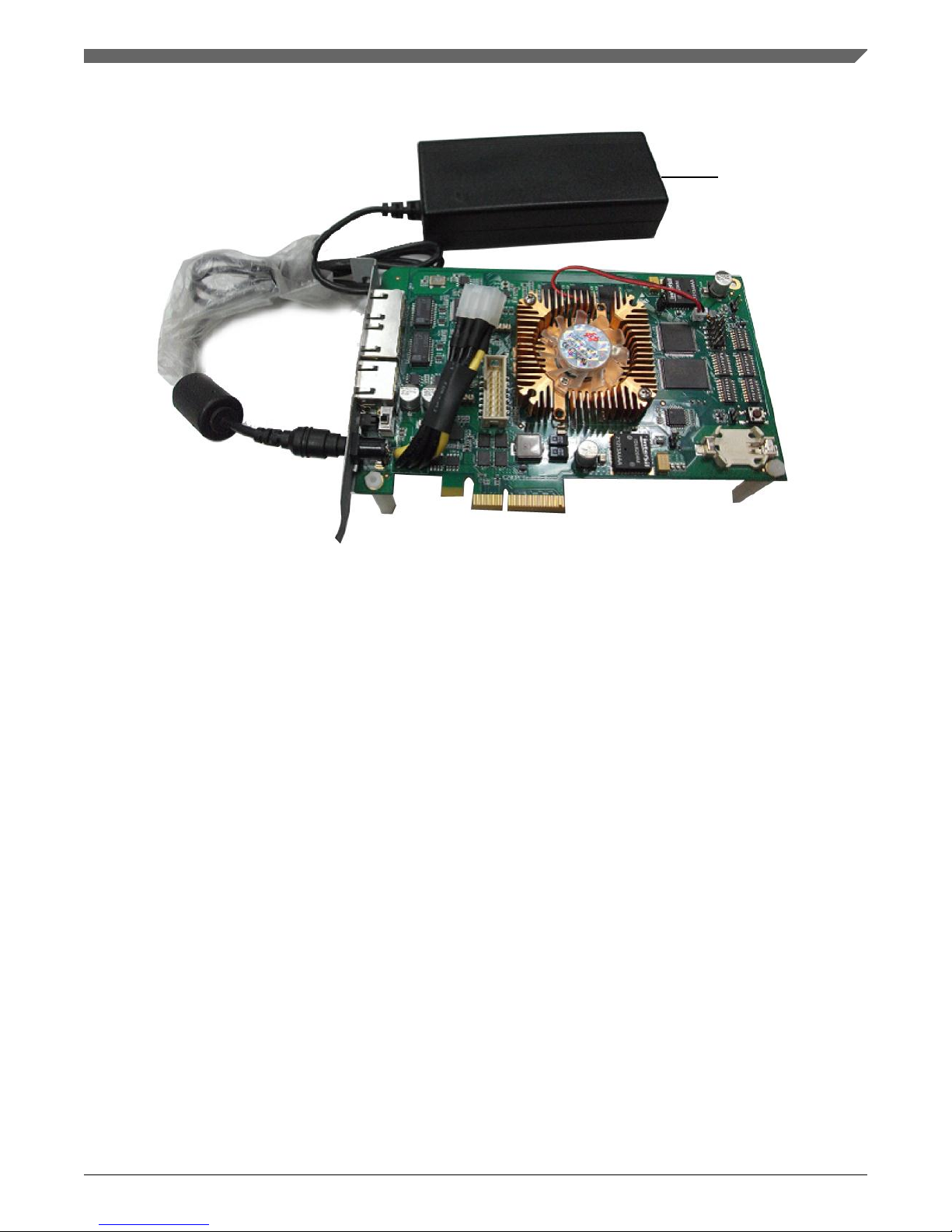
The C29x PCIe is a PCIe card with a Freescale C29x crypto coprocessor system-on-chip
(SoC)/processor.
1.1 Acronyms
The table below lists and explains the acronyms used in this document.
Table 1-1. Acronyms
Term Description
COP Common On-Chip Processor
CTS Clear-To-Send
DIP Dual In-Line Package
ECC Elliptic Curve Cryptography
EP Endpoint
eTSEC Enhanced Three-Speed Ethernet Controller
I2C Inter-Integrated Circuit
IFC Integrated Flash Controller
POR Power-On-Reset
RC Root Complex
RGMII Reduced Gigabit Media Independent Interface
RMII Reduced Media Independent Interface
RTS Ready-To-Send
SerDes Serializer/Deserializer
SoC System-On-Chip
SPI Serial Peripheral Interface
UART Universal Asynchronous Receiver/Transmitter
C29x PCIe Card User Guide, Rev. 0, 10/2013
Freescale Semiconductor, Inc. 7
Page 8

1.2 Related Documentation
The table below lists and explains the additional documents that you can refer to, for
more information about C29x PCIe.
Table 1-2. Related documentation
Document Description
C29x Crypto Coprocessor Family
Reference Manual
Defines the functionality of the Freescale C29x family. Freescale C29x family consists
of three highly integrated security processors, optimized for public key acceleration and
secure key management. Each family member combines a Power Architecture
processor core with a high performance security engine, network and high-speed serial
interfaces, DDR and non-volatile memory controllers.
C29x Crypto Offload User Guide Explains the procedure to build, configure, and use different software components for
the Freescale C29x crypto coprocessor device.
C29x PCIe Card Getting Started
Guide
Explains C29x PCIe board settings and physical connections needed to boot the board.
Freescale C29x Crypto Coprocessor
Family Product Brief
Provides an overview of the Freescale C29x family of crypto coprocessor features, and
examples of C29x usage.
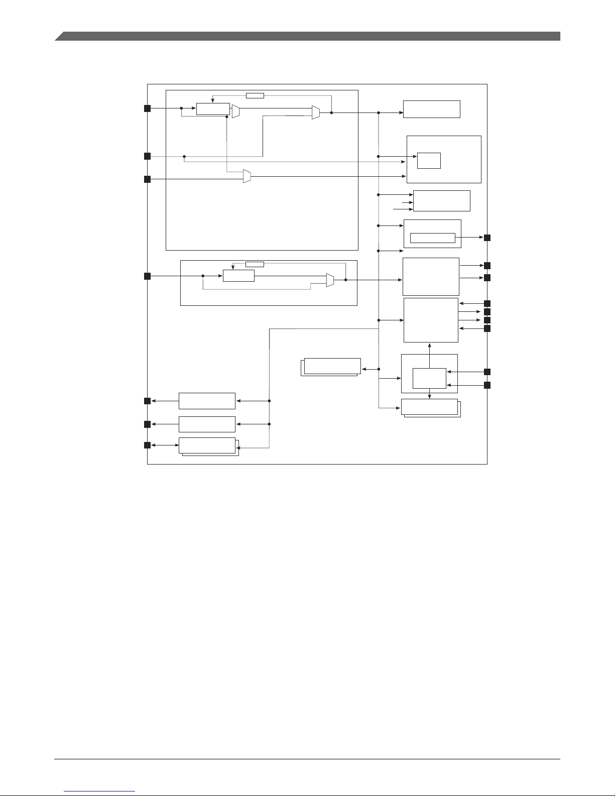
1.3 Architectural Overview
The figure below shows the block diagram of C29x.
Architectural Overview
C29x PCIe Card User Guide, Rev. 0, 10/2013
8 Freescale Semiconductor, Inc.
Page 9
C29x
Security Fuse Processor
Security Monitor
IFC
Power Management
eSDHC
2x DUART
2x I2C
eSPI, GPIO
Power Architecture
e500-v2 Core
TM
32 KB
D-Cache
32 KB
I-Cache
512 KB
Platform Cache
32-bit
DDR3/3L
Memory
Controller
SEC1
SEC2
SEC3
Coherent System Bus
512 KB
Platfrom
SRAM
eTSEC
eTSEC
4-lane 5 GHz SerDes
PCle
DMA
Real Time Debug
JTAG
Figure 1-1. C29x block diagram
The figure below shows the block diagram of the C29x PCIe card.
Magnetics
Magnetics
RS232
RJ45
(Console)
RJ45 x2 (Ethernet)
MDI
RS232
XCVR
UART
GE PHY
VSC8641
MDIO
RGMII
DUART
RGMII
C29x
IFC
I2C
SerDes
JTAG
SPI
COP
Connector
PCle x4
EEPROM
S25FL 128
SPI IF
I2C IF
Thermal
Monitor
EEPROM
AT24C1024
CORE POWER
12V
PCle Finger
Power
Select
Circuit
12V
Power Jack
Super
Sequencer
Power
Regulators
1.0V
Configs
CPLD
NAND Flash
(4 GB)
NOR Flash
(64 MB)
DDR3
(512 MB)
32-bit
Reset
Watch Dog
GE PHY
VSC8641
MDI
Resets
12V
1.5V
GVDD
VTT
3.3V
2.5V
16-bit
8-bit 8-bit
LFC_Data(15:0)/Add(27:0)
TSEC1
DDR
TSEC2
Figure 1-2. C29x PCIe card block diagram
Chapter 1 Introduction
C29x PCIe Card User Guide, Rev. 0, 10/2013
Freescale Semiconductor, Inc. 9
Page 10

The C29x PCIe card provides the following integrated functions:
• External interfaces
• One X4 PCIe Gen1 interface
• Two 1 Gb RGMII Ethernet ports
• One RJ45 serial console port that supports one UART up to 115200 bps for
console display
• One JTAG debug interface
• On-board memories
• 64 MB 16-bit NOR flash memory of S29GL512P11TFI0
• 4 GB 8-bit NAND flash memory of K9GBG08U0A
• 512 MB 32-bit DDR3 memory of MT41J128M16
• 16 Mb SPI EEPROM of S25FL128
• Power supplies
• External 12V DC power input
• 2x3 6-pin power connector for ATX power supply
• Headers
• Connector for ADM1069 (power-on control chipset) programming
• Connector for CPLD programming
• Connector for ZL6105 (digital power) programming
• POR configuration
• Supports critical POR settings through DIP switches available on the board
1.4 Board Drawing and Top View
The figure below shows C29x PCIe top side reference drawing.
Board Drawing and Top View
C29x PCIe Card User Guide, Rev. 0, 10/2013
10 Freescale Semiconductor, Inc.
Page 11
Figure 1-3. Top side reference drawing
The C29x PCIe card measures 168 mm x 111 mm. It can be installed into a PCIe-x4,
PCIe-x8, or PCIe-x16 slot on the PCIe motherboard.
The figure below shows the top view of the C29x PCIe card.
Chapter 1 Introduction
C29x PCIe Card User Guide, Rev. 0, 10/2013
Freescale Semiconductor, Inc. 11
Page 12
2x3 ATX Power
Connector
PCIe x4 Gold-finger
ON/OFF
Switch
Power
LED
UART
ETH1
TSEC2
ETH0
TSEC1
J16
J15
DIP
Switch
J18
for Fan
JTAG
Figure 1-4. C29x PCIe card top view
Board Drawing and Top View
C29x PCIe Card User Guide, Rev. 0, 10/2013
12 Freescale Semiconductor, Inc.
Page 13
Chapter 2
PCIe Use Cases
This chapter talks about:
•
PCIe endpoint mode
• Standalone host mode
• PKCAL/SKMM mode
• Secure boot mode
2.1 PCIe Endpoint Mode
The figure below shows the C29x PCIe card, operating in the PCIe endpoint mode.
Figure 2-1. PCIe endpoint mode
Perform the following steps to use the C29x PCIe card in the PCIe endpoint mode:
1.
Connect the heat sink fan power line to J18.
2. Plug C29x PCIe into the PCIe slot on the motherboard. C29x PCIe supports x1, x2,
and x4 configurations.
C29x PCIe Card User Guide, Rev. 0, 10/2013
Freescale Semiconductor, Inc. 13
Page 14

3. Connect 2x3 ATX power connector to the ATX power supply of the computer, if
ATX power supply is installed in the computer; otherwise, connect the 12V power
adapter.
4. Connect the RJ45 console line (RJ45 to DB9 cable used) to UART port.
5. Configure the serial port of the attached computer with the following values:
• Data rate: 115200 bps
• Number of data bits: 8
• Parity: None
• Number of stop bits: 1
• Flow control: Hardware/None
6. Connect network cable to TSEC1.
7. Power on host motherboard and put the power switch to ON position. Now, you will
see the boot up message on the computer console.
Following are the device configurations required for this use case by setting DIP switch:
• SW7[1] ON, cfg_cpu_boot=0
• SW7[5] ON, cfg_host_agt=0
The table below shows dual in-line package (DIP) switch settings of the C29x PCIe card
in PCIe endpoint mode (800 MHz core, 400 MHz platform, PCIe-x4 configuration).
Table 2-1. PCIe endpoint mode DIP switch settings
SW4[1..8] 0101 1000 ON OFF ON OFF OFF ON ON ON
SW5[1..8] 1111 0000 OFF OFF OFF OFF ON ON ON ON
SW6[1..8] 0000 1111 ON ON ON ON OFF OFF OFF OFF
SW7[1..8] 0001 0111 ON ON ON OFF ON OFF OFF OFF
SW8[1..8] 0000 1011 ON ON ON ON OFF ON OFF OFF
NOTE
If your host does not recognize the card when performing lspci,
then try changing the PCIe lane configuration.
2.2 Standalone Host Mode
The figure below shows the C29x PCIe card, operating in standalone host mode (without
the host computer).
Standalone Host Mode
C29x PCIe Card User Guide, Rev. 0, 10/2013
14 Freescale Semiconductor, Inc.
Page 15
100~240V AC
Figure 2-2. Standalone host mode
Perform the following steps to use the C29x PCIe card in the standalone host mode:
1.
Remove PCIe bracker, and install four plastic posts.
2. Connect heat sink fan power line to J18.
3. Connect 12V power supply.
4. Connect RJ45 console line to UART port.
5. Configure the serial port of the attached computer with the following values:
• Data rate: 115200 bps
• Number of data bits: 8
• Parity: None
• Number of stop bits: 1
• Flow control: Hardware/None
6. Connect network cable to TSEC1.
7. Turn on ON/OFF switch to power on C29x PCIe. Now, you will see C29x PCIe boot
up message on the computer console.
Following are the device configurations required for this use case by setting DIP switch:
• SW7[1] OFF, cfg_cpu_boot=1
The table below shows DIP switch settings of the C29x PCIe board in the standalone
mode (800 MHz core, 400 MHz platform, PCIe-x4 configuration). As compared to the
end point mode, in the standalone mode, SW7[1] is in OFF position.
Chapter 2 PCIe Use Cases
C29x PCIe Card User Guide, Rev. 0, 10/2013
Freescale Semiconductor, Inc. 15
Page 16

Table 2-2. Standalone host mode DIP switch settings
SW4[1..8] 0101 1000 ON OFF ON OFF OFF ON ON ON
SW5[1..8] 1111 0000 OFF OFF OFF OFF ON ON ON ON
SW6[1..8] 0000 1111 ON ON ON ON OFF OFF OFF OFF
SW7[1..8] 1001 1000 OFF ON ON OFF ON OFF OFF OFF
SW8[1..8] 0000 1011 ON ON ON ON OFF ON OFF OFF
2.3 PKCAL/SKMM Mode
PKCAL means Public Key Calculator, which is one use case of PCIe endpoint mode.
SKMM means Secure Key Management Module. In this document, SKMM only means
the core does NOT boot from internal SDRAM. In PKCAL mode, the board holds and
wait for the host to load the image into its internal SDRAM, then the host, which is
released, lets the board to run.
In SKMM mode, the board runs the u-boot and loads the Linux by itself while working in
PCIe end point mode. The host can communicate with PCIe interface. The PKCAL/
SKMM mode can be enabled by setting the SW8[8] switch. To enable the PKCAL mode,
set SW8[8] to 0. To enable the SKMM mode, set SW8[8] to 1.
The PKCAL mode can be started from the PCIe endpoint mode. In PKCAL mode, a
C29x processor only uses internal SDRAM, instead of DDR3/NOR flash/NAND flash.
Therefore, DDR/NOR flash/NAND flash should not be initialized in the source code. In
addition, the PKCAL mode requires the board to be booted from the PCIe slot.
For the PKCAL use case, the device boots from either the internal SRAM or the L2
SRAM. The device is in PCI Express agent mode and e500 is in boot hold off. Following
are the device configurations required for this use case by setting DIP switch:
• SW7[1] ON, cfg_cpu_boot=0
• SW7[5] ON, cfg_host_agt=0
• SW8[8] ON, test_sel_b=0
By default, the C29x PCIe card works in the SKMM mode.
PKCAL/SKMM Mode
C29x PCIe Card User Guide, Rev. 0, 10/2013
16 Freescale Semiconductor, Inc.
Page 17

2.4 Secure Boot Mode
C29x supply Secure Boot mode to protect customer system. The customer can put
secured encoded u-boot and other image into flash, and put the secure key into C29x
silicon. If secured keys are matched, the image can be loaded and run. The secure boot
mode can be enabled by setting SW7[6] to ON and cfg_sb_dis to 0.
The secure boot mode can be started from the PCIe endpoint mode and standalone host
mode.
To start the secure boot mode from the PCIe endpoint mode, connect J15 and J16 (pin 1
and pin 2). The board will now support secure boot from NOR flash, NAND flash, or SPI
EEPROM.
To start the secure boot mode from the standalone host mode, connect J16 (pin 1 and pin
2), and install the battery. The board will now support secure boot from NOR flash,
NAND flash, or SPI EEPROM.
Following are the device configurations required for this use case by setting DIP switch:
• SW7[6] = ON, cfg_sb_dis=0
The table below lists the secure boot POR settings example in NOR flash boot mode (800
MHz core, 800 MHz DDR, PCIe-x4 agent).
Table 2-3. Secure POR settings
SW4[1..8] 0101 1000 ON OFF ON OFF OFF ON ON ON
SW5[1..8] 1111 1000 OFF OFF OFF OFF OFF ON ON ON
SW6[1..8] 0000 1111 ON ON ON ON OFF OFF OFF OFF
SW7[1..8] 0001 0011 ON ON ON OFF ON ON OFF OFF
SW8[1..8] 0000 1011 ON ON ON ON OFF ON OFF OFF
Chapter 2 PCIe Use Cases
C29x PCIe Card User Guide, Rev. 0, 10/2013
Freescale Semiconductor, Inc. 17
Page 18

Secure Boot Mode
C29x PCIe Card User Guide, Rev. 0, 10/2013
18 Freescale Semiconductor, Inc.
Page 19

Chapter 3
Clocks, Resets, and Power Control
3.1 Clocks
The figure below shows the C29x PCIe input clocks.
C29x PCIe Card User Guide, Rev. 0, 10/2013
Freescale Semiconductor, Inc. 19
Page 20
TCK/TSTCLK
SYSCLK
(66 MHz - 100 MHz)
(207 MHz - 400 MHz)
RTC/CORE_BYPASS_CLK
COP
DDR_CLK
DDR PHY
PLL
(800 MHz - 1300 MHz)
SDHC_CLK
SPI_CLK
IIC[1-2]_SCL
PLL
Lynx(x4)
SD_REF_CLK_B
(100 MHz or 125 MHz)
SD_REF_CLK
(100 MHz or 125 MHz)
EC_GTX_CLK125
EC_MDC
TSEC_GTX_CLK
TSEC_RX_CLK
eTSEC
DDR
/4, 8, /16
MCK_B
MCK
LCK[0:1]
(10 MHz - 100 MHz)
IFC
SAP
tck_nog
tck
PLL
e500 Core
Complex
L2
idcp_ipg_clk
div
PLL
SPI
eSDHC
I2C
CAAMs,
Other IPs
PCI-EX
div
Figure 3-1. C29x PCIe input clocks
In the above figure:
•
SYSCLK is a 66.67 MHz primary clock
• DDR_CLK is 100 MHz external clock
• SD_REFCLK is 100 MHz, required for PCIe interface
• TSEC_RX_CLK is 125 MHz, required for GE port
• CPLD_REFCLK is 32.768 kHz, required for CPLD to work
Resets
C29x PCIe Card User Guide, Rev. 0, 10/2013
20 Freescale Semiconductor, Inc.
Page 21

3.2 Resets
All resets for the C29x PCIe card are handled by CPLD. A power-on-reset is initiated by
pressing the power switch, if the board is in a chassis. A warm reset is initiated by
pressing SW1 on the board. A warm reset can also be initiated using software, by
asserting the HRESET_REQ line from the processor.
The figure below shows the reset block of C29x PCIe.
PS_RST_N
ADM1069
(Power Monitor)
GND
Push-Button
MAX811S
(Power-on RST)
PON_RST_N
WD_CFG0
WDO N
WDI
MAX6370
(Watch_Dog)
COP_ITF
COP_SRST_N
COP_HRST_N
HRSET_N
HRSET_REQ_N
C29x
AND
CPLD
Soft reset register
AND
GE2_RST_N
GE2
PHY
NOR
FLASH
DDR3/
DDR3L
WD_CFG1
WD_CFG2
GE1_RST_N
AND
GE1
PHY
7
6
5
4
3
2
1
0
Figure 3-2. C29x PCIe reset block
3.3 Power Block Diagram
The figure below shows the power block diagram of the C29x PCIe board.
Chapter 3 Clocks, Resets, and Power Control
C29x PCIe Card User Guide, Rev. 0, 10/2013
Freescale Semiconductor, Inc. 21
Page 22

PEX_12V
JACK_12V
Power Select
12V
PS_1V0_EN
ZL6105
1V@30A
Ferrite
Bead
GND
Connect VDD_CA to GND for C291
Connect VDD_CB to GND
for C291 and C292
3V3_AUX
Battery
PS_3V3_EN
ADM1069
(Power monitor and
power-on sequence)
12V
Filter
MAX8869
(LDO)
ISL8204M
PS_VTT_EN
MAX8869
(LDO)
TPS51200
1V5/1V35@4A
ISL8204M
PS_GVDD_EN
12V
Ferrite
Bead
Ferrite
Bead
Ferrite
Bead
Filter
GND
GND
GND
1V
1.5V
2.5V
12V
3V3@4A
1V0
GVDD
2V5
3V3
1V5
NCP571
SN10T1G
1V0
1V0_AVDD_DDR
1V0_AVDD_PLAT
1V0_SD_AVDD
1V0_SVDD
1V0_AVDD_CORE
1V0_LP
LP_TMP_DET_N
1V5_XVDD
GVDD
2V5
VTT
MVREF
3V3
1V0_CA
1V0_CB
(VDDC, VDD, VDD_LL)
(AVDD_DDR)
(AVDD_CORE)
(AVDD_PLAT)
(AVDD_SD_PLL1)
(SVDD)
(VDD_CA)
(VDD_CB)
(VDD_LP)
(XVDD)
For C29x:
2V5: LVDD
3V3: OVDD, 02VDD, BVDD, CVDD
(GVDD)
Figure 3-3. Power block diagram
Power Block Diagram
C29x PCIe Card User Guide, Rev. 0, 10/2013
22 Freescale Semiconductor, Inc.
Page 23

Chapter 4
On-Board Resources
The C29x PCIe card supports the following on-board resources:
•
DDR memories
• Integrated flash controller (IFC)
• SerDes
• Ethernet
• eSPI
• RS-232
All these on-board resources are described, one by one, in the subsections that follow.
4.1 DDR Memories
The C29x PCIe card supports DDR3 and DDR3L memories. The memory interface on
the board is configured as DDR3/DDR3L. The DDR3/DDR3L memory and ECC are
implemented as a single bank discrete chipset (x16).
When DDR3 chipset is assembled, the jumper J12 is connected to set the GVDD supply
to 1.5V DC, or is disconnected to set GVDD to 1.35V DC.
The memory size supported on the board is 512 MB ((2 chips * 2 Gbit chips)/8bits).
The figure below shows the DDR3/DDR3L SDRAM controller connection.
C29x PCIe Card User Guide, Rev. 0, 10/2013
Freescale Semiconductor, Inc. 23
Page 24

ECC[0:7]
DDR3/DDR3L Device
with ECC
C29X
DDR3/DDR3L
Controller
VTT
VREF
40.2 Ohm
MCS[0:1]_N
MCK_P/N, MCKE[0:1]
MRAS_N, MCAS_N, MWE_N
A[0:15], BA[0:2]
MDQ[0:31]
DQS[0:1]_P, DQS[0:1]_N
MDM[0:1]
RST_N
ODT[0:1]
VREF
Figure 4-1. DDR3/DDR3L memory
NOTE
The DDR3/DDR3L address, control, and command signals are
terminated to the VTT rail, using a 40.2Ω resistor.
4.2 IFC
The C29x PCIe card supports the following two IFC resources:
•
NOR flash memory
• NAND flash memory
4.2.1 NOR Flash Memory
The C29x PCIe card provides NOR flash memory of 64 MB with 16-bit port size. The
figure below shows the hardware connection between the C29x PCIe card and NOR flash
memory.
IFC
C29x PCIe Card User Guide, Rev. 0, 10/2013
24 Freescale Semiconductor, Inc.
Page 25

IFC
Controller
IFC_AD[15:0]
C29x
IFC_ADDR[26:4]
IFC_ADDR[3]
IFC_ADDR[2]
IFC_WE_B
IFC_OE_B
FBANK_SEL2
SW5[8]
NOR_CS_B
CE
NOR
Flash 16-Bit
DQ[0:15]
A[0:22]
A[23`]
A[24]
WE_B
OE_B
U10
SN74LVC1G86DBVR
FBANK_SEL1
SW5[7]
5
4
3
1
2
10
11
VCC
O
GND
U42
5
4
3
1
2
10
11
VCC
O
GND
SN74LVC1G86DBVR
Figure 4-2. NOR flash memory
NOTE
In the above figure, NOR_CS can be either CS0 or CS1
depending on the boot location. It is set using SW5[6].
The NOR flash memory is divided into four memory banks with 16 MB size each. The
DIP switch, SW5[7:8], can be used to change the starting address for the memory banks.
Four different u-boot images can be programmed into each memory bank. When
selecting NOR flash as boot flash (CS0 is connected to NOR flash by setting SW5[6] to
ON, rom_location is set to 1111 using SW5[1:4]), different u-boot images can be selected
to boot up the board, by setting SW5[7:8].
4.2.2 NAND Flash Memory
The C29x PCIe provides NAND flash memory of 4 GB with 8-bit port size. The figure
below shows the hardware connectivity between the C29x PCIe card and NAND flash
memory.
Chapter 4 On-Board Resources
C29x PCIe Card User Guide, Rev. 0, 10/2013
Freescale Semiconductor, Inc. 25
Page 26

IFC
Controller
C29X
IFC_CLE
IFC_AVD
IFC_WE_B
IFC_OE_B
IFC_WP_B
IFC_RB0_B
IFC_RB1_B
IFC_AD[0:7]
CPLD
NAND_CS_B
NAND
Flash 8-Bit
CE_B
CLE
ALE
WE
RE_B
WP_B
RY/BY_B
IO[7:0]
Figure 4-3. NAND flash memory
NOTE
In the above figure, NAND_CS can be either CS0 or CS1
depending on the boot location. It is set using SW5[6].
If connecting NAND flash to CS0, set SW5[6] to OFF, and connect RY/BY_N signal to
IFC_RB0_N. If connecting NAND flash to CS1, set SW5[6] to ON, and connect RY/
BY_N signal to IFC_RB1_N.
4.3 SerDes
On the C29x PCIe card, the SerDes module implements link serialization/deserialization
and PCS functions for a PCI express link, operating at 2.5 or 5 Gbaud.
The table below shows the different settings for SerDes.
Table 4-1. SerDes settings
Functional
signal
Reset
configuration
name
Value (binary) 4-lane Lynx 23
A B E F
IFC_AD[13:14],
IFC_BCTL
Default (111)
cfg_io_ports[0:2] 000 PCIe-x4 (5 GHz)
001 PCIe-x4 (2.5 GHz)
010 PCIe-x2 (5 GHz) Disabled Disabled
011 PCIe-x2 (2.5 GHz) Disabled Disabled
100 PCIe-x1 (5 GHz) Disabled Disabled Disabled
101 PCIe-x1 (2.5
GHz)
Disabled Disabled Disabled
110 Reserved
Table continues on the next page...
SerDes
C29x PCIe Card User Guide, Rev. 0, 10/2013
26 Freescale Semiconductor, Inc.
Page 27

Table 4-1. SerDes settings (continued)
Functional
signal
Reset
configuration
name
Value (binary) 4-lane Lynx 23
A B E F
111 Disabled Disabled Disabled Disabled
The table above shows that:
• All SerDes lanes are configured as a PCIe-x4 interface
• Lane A and lane B are configured as a PCIe-x2 interface
• Lane A is configured as a PCIe-x1 interface
These interfaces are compliant with the PCI Express Base Specification Revision 2.0,
which supports root complex (RC) and endpoint (EP) configurations.
4.4 Ethernet
The C29x PCIe card supports a maximum of two Ethernet ports.
4.4.1 eTSEC1
eTSEC1 10/100/1000 BaseT operates in the RGMII mode, and is directly connected to a
Vitesse RGMII PHY (VSC8641), as shown in the figure below.
C29x
eTSEC1
RGMII
MDC, MDIO
VSC8641
GBE PHY
MDIO PHY
Address = 2
RJ-45 Port
Figure 4-4. eTSEC1
Chapter 4 On-Board Resources
C29x PCIe Card User Guide, Rev. 0, 10/2013
Freescale Semiconductor, Inc. 27
Page 28

4.4.2 eTSEC2
eTSEC2 10/100/1000 BaseT operates in the RGMII mode, and is directly connected to a
Vitesse RGMII PHY (VSC8641), as shown in the figure below.
C29x
eTSEC2
RGMII
MDC, MDIO
VSC8641
GBE PHY
MDIO PHY
Address = 0
RJ-45 Port
Figure 4-5. eTSEC2
4.5 eSPI
The eSPI is a full-duplex, synchronous, character-oriented channel that supports a fourwire interface (receive, transmit, clock, and slave select). The C29x processor has the
ability to boot from an SPI serial flash device, in addition to supporting other peripheral
devices conforming to the SPI standard. A Spansion SPI flash memory is supported on
the board.
4.6 RS-232
The C29x processor has two UART controllers. However, due to space limitations, the
C29x PCIe card supplies only one RS-232, which provides an RS-232 standard
interconnection between the board and an external host. The serial connection is typically
configured to run at 115.2 Kbps.
Each UART supports:
•
Full-duplex operation
• Software-programmable baud generators:
• Divide the input clock by 1 to (216 - 1)
• Generate a 16x clock for the transmitter and receiver engines
• Clear-to-send (CTS) and ready-to-send (RTS) modem control functions
• Software-selectable serial interface data format that includes:
eSPI
C29x PCIe Card User Guide, Rev. 0, 10/2013
28 Freescale Semiconductor, Inc.
Page 29

• Data length
• Parity
• 1/1.5/2 STOP bit
• Baud rate
• Overrun, parity, and framing error detection
The UART ports are routed to RJ45 connectors, as shown in the figure below.
C29x
UART1
CTS
RXD
TXD
RTS
CTS
RXD
TXD
RTS
MAX3232EUE+
DO
DO
D1
D1
RX
RX
RX
RX
CTS
RXD
TXD
RTS
1
2
3
4
5
6
7
8
J23
9
RJ45
10
UART0
Figure 4-6. RS-232
The table below shows the connection settings for the UART RJ45 to DB9 female cable
connections.
Table 4-2. RJ45 to DB9 female connection settings
RJ45 pin number RS-232 signal DB9 female pin number
1 RTS 8
2 NC
3 TXD 2
4 GND
5 GND 5
6 RXD 3
7 NC
8 CTS 7
Before powering up the C29x PCIe card, configure the serial port of the attached
computer with the following values:
• Data rate: 115200 bps
Chapter 4 On-Board Resources
C29x PCIe Card User Guide, Rev. 0, 10/2013
Freescale Semiconductor, Inc. 29
Page 30

• Number of data bits: 8
• Parity: None
• Number of stop bits: 1
• Flow control: Hardware/None
RS-232
C29x PCIe Card User Guide, Rev. 0, 10/2013
30 Freescale Semiconductor, Inc.
Page 31

Chapter 5
Board Connectors, LED, and Push Button
5.1 Connectors
The below table details all the connectors on the C29x PCIe card.
Table 5-1. Connector settings
Reference designator Description Notes
J2 GE1 and GE2 Ethernet ports First port: TSEC1 (RGMII) -> VSC8641
Second port: TSEC2 (RGMII) -> VSC8641
J23 UART UART0 -> ICL3232
J13 External 12V DC External 12V DC connector
5.2 Headers
The below table details all header connectors on the C29x PCIe card.
Table 5-2. Header settings
Reference designator Description Notes
J3 JTAG/COP connector Used for PowerPC JTAG
J10 ZL6105 program port Digital power chipset (ZL6105) I2C interface for programming
J17 ADM1069 program port Power-on control and power monitor chipset (ADM1069) program port
J18 Fan port Fan power supply (12V DC) and speed control interface
J9 CPLD header Used for programming the ALTERA CPLD device
5.3 Jumpers
The below table details jumpers on the C29x PCIe adapter board.
C29x PCIe Card User Guide, Rev. 0, 10/2013
Freescale Semiconductor, Inc. 31
Page 32

Table 5-3. Jumper settings
Reference designator Description Status 1 Status 2
J15 Battery selection for VDD_LP
source
Mounted: Battery acts as a
VDD_LP input source
Unmounted: Battery is
disconnected
J16 Tamper detection pin powered
selection
1-2: Tamper detection pin
powered on
2-3: Tamper detection pin
powered off
J13 GVDD voltage selection Mounted: GVDD=1.5V for
DDR3
Unmounted: GVDD=1.35V for
DDR3L
J19 Fan speed control Mounted: Fan is in full speed
mode
Unmounted: Fan speed is
controlled by CPLD
5.4 JTAG/COP Connector
The JTAG connection is provided by a direct connection to the appropriate header
connector.
COP is a part of the C29x's JTAG module and is implemented as a set of additional
instructions and logic. This port can connect to a dedicated emulator for extensive system
debugging. Several third-party emulators available in the market can connect to the host
computer using the Ethernet port, USB port, parallel port, RS-232, and so on.
The figure below shows a typical setup for the COP connector using a USB port
emulator.
PC
COP Port
C29x PCIe Card
USB
Emulator
USB Port
Figure 5-1. COP connector setup
A 16-pin generic header connector carries the JTAG/COP signals and additional signals
for system debugging. The pinout of this connector is shown in the figure below.
JTAG/COP Connector
C29x PCIe Card User Guide, Rev. 0, 10/2013
32 Freescale Semiconductor, Inc.
Page 33

TDO
TDI
NC
TMS
SRESET_B
HRESET_B
CKSTP_OUT
TCK
1
NC
TRST_B
VDD_SENSE
NC
GND
NC
GND
CKSTP_IN
Figure 5-2. Pinout for COP connector
The connections made from the COP connector are shown in the table below.
Table 5-4. COP connector settings
Pin number Signal name Connection
1 TDO Connected directly between the processor and JTAG/COP connector.
2 NC Not connected.
3 TDI Connected directly between the processor and JTAG/COP connector.
4 TRST Routed to the RESET PLD. TRST to the processor is generated from the PLD.
5 NC Not connected.
6 VDD_SENSE Pulled to 3.3 V through a 10Ω resistor.
7 TCK Connected directly between the processor and JTAG/COP connector.
8 CKSTP_IN Connected directly between the processor and JTAG/COP connector.
9 TMS Connected directly between the processor and JTAG/COP connector.
10 NC Not connected.
11 SRESET Routed to the RESET PLD. SRESET to the processor is generated from the PLD.
12 GND Connected to ground.
13 HRESET Routed to the RESET PLD. HRESET to the processor is generated from the PLD.
14 KEY Not connected.
15 CKSTP_OUT Connected directly between the processor and JTAG/COP connector.
16 GND Connected to ground.
5.5 LED
The table below details LED settings for the C29x PCIe card.
Table 5-5. LED settings
Reference designator Used for Notes
D3 Indicating the status of C29x PCIe Sold green: Power-on is ok
Chapter 5 Board Connectors, LED, and Push Button
C29x PCIe Card User Guide, Rev. 0, 10/2013
Freescale Semiconductor, Inc. 33
Page 34

Table 5-5. LED settings
Reference designator Used for Notes
Flash green: Software boot is ok
5.6 Push Button
The push button SW1 on the C29x PCIe card is used for reset.
Push Button
C29x PCIe Card User Guide, Rev. 0, 10/2013
34 Freescale Semiconductor, Inc.
Page 35

Chapter 6
POR Configuration
The C29x PCIe card has user selectable switches or registers, for evaluating different
frequency and boot configuration for this device. The table below shows how POR
configuration is done through switches.
Table 6-1. POR configuration through switches
Switch POR
configuration
Signal name Default
setting
Signal meaning Settings
SW4[1] cfg_sys_pll[0] IFC_AD0 ON Rate between
SYSCLK input and
CCB clock (platform
clock)
SW4[1,2,3] ON ON ON (000): 4:1
SW4[1,2,3] ON ON OFF (001): 5:1
SW4[1,2,3] ON OFF ON (010): 6:1
Others are reserved.
SYSCLK on this board is 66.67 MHz.
SW4[2] cfg_sys_pll[1] IFC_AD1 OFF
SW4[3] cfg_sys_pll[2] IFC_AD2 ON
SW4[4] cfg_sys_speed READY OFF 0: SYSCLK frequency is at or below 66
MHz.
1: SYSCLK frequency is above 66
MHz.
SW4[5] cfg_core_pll[0] IFC_AD3 OFF Ratio between the
e500 core clock and
e500 CCB clock
SW4[5,6,7] ON ON ON (000): reserved
SW4[5,6,7] ON ON OFF (001):
reserved
SW4[5,6,7] ON OFF ON (010): 1:1
SW4[5,6,7] ON OFF OFF (011): 1.5:1
SW4[5,6,7] OFF ON ON (100): 2:1
SW4[5,6,7] OFF ON OFF (101): 2.5:1
SW4[5,6,7] OFF OFF ON (110): 3:1
SW4[5,6,7] OFF OFF OFF (111): 3.5:1
SW4[6] cfg_core_pll[1] IFC_AD4 ON
SW4[7] cfg_core_pll[2] IFC_AD5 ON
SW4[8] cfg_core_speed IFC_AD6 ON Core speed
configuration input
ON(0): Core clock frequency is greater
than or equal to 600 MHz and less than
1001 MHz.
OFF(1): Core clock frequency is
greater than or equal to 1001 MHz and
less than 1201 MHz.
SW5[1] SW_CFG_ROM_
LOC0
OFF Boot ROM location SW5[1:4] ON ON OFF ON (0010): 8b
NAND (8k page size)
Table continues on the next page...
C29x PCIe Card User Guide, Rev. 0, 10/2013
Freescale Semiconductor, Inc. 35
Page 36

Table 6-1. POR configuration through switches
(continued)
Switch POR
configuration
Signal name Default
setting
Signal meaning Settings
SW5[2] SW_CFG_ROM_
LOC1
SW5[1:4] ON OFF ON ON (0100):
DDR controller
SW5[1:4] ON OFF OFF ON (0110): SPI
SW5[1:4] ON OFF OFF OFF (0111):
SDHC (SD/MMC)
SW5[1:4] OFF ON ON ON (1000): 8b
NAND (512 page size)
SW5[1:4] OFF ON ON OFF (1001): 8b
NAND (2k page size)
SW5[1:4] OFF ON OFF OFF (1011): 8b
NOR
SW5[1:4] OFF OFF ON ON (1100):
16b NAND (512 page size)
SW5[1:4] OFF OFF ON OFF (1101):
16b NAND (2k page size)
SW5[1:4] OFF OFF OFF OFF (1111):
16b NOR
Others are reserved.
OFF
SW5[3] SW_CFG_ROM_
LOC2
OFF
SW5[4] SW_CFG_ROM_
LOC3
OFF
SW5[5] VCORE_MGN ON ON(0): CPU will run at v1.0 core
voltage
OFF(1): CPU will run at v1.05 core
voltage
SW5[6] BOOT_FLASH_SELON CS0/1 select ON (0): CS0 is connected to NOR
flash; CS1 is connect to NAND flash.
OFF (1): CS0 is connected to NAND
flash; CS1 is connected to NOR flash.
SW5[7] FBANK_SEL1 ON NOR boot section
choose
Set which section works as a boot
section.
SW5[8] FBANK_SEL2 ON
SW6[1] cfg_ddr_pll[0] SW_TSEC1_TXD0ON Clock ratio between
100Mhz OSC clock
input and DDR
complex clock
SW6[1,2,3] ON ON ON (000): 8:1
SW6[1,2,3] ON ON OFF (001): 10:1
SW6[1,2,3] ON OFF ON (010): 12:1
SW6[1,2,3] ON OFF OFF (011): 13:1
SW6[1,2,3] OFF ON ON (100): 14:1
SW6[1,2,3] OFF ON OFF (101): 15:1
SW6[1,2,3] OFF OFF ON (110): 16:1
SW6[1,2,3] OFF OFF OFF (111):
Reserved
SW6[2] cfg_ddr_pll[1] SW_TSEC1_TXD1ON
SW6[3] cfg_ddr_pll[2] UART1_RTS_N ON
SW6[4] cfg_ddr_speed[0] 1588_CLK_OUT ON DDR complex speed
configuration input
cfg_ddr_speed[0]:
ON (0): DDR data rate is less than 967
MHz.
SW6[5] cfg_ddr_speed[1] 1588_PULSE_OUTOFF
Table continues on the next page...
C29x PCIe Card User Guide, Rev. 0, 10/2013
36 Freescale Semiconductor, Inc.
Page 37

Table 6-1. POR configuration through switches
(continued)
Switch POR
configuration
Signal name Default
setting
Signal meaning Settings
OFF (1): DDR data rate is greater than
or equal to 967 MHz.
cfg_ddr_speed[1]:
ON (0): When cfg_ddr_speed[0]=1 and
cfg_ddr_pll=10
OFF (1): When cfg_ddr_speed[0]=0
and (cfg_ddr_pll=8 or cfg_ddr_pll=10 or
cfg_ddr_pll>=12) or when
cfg_ddr_speed[0]=1 and
cfg_ddr_pll>=12
NA: When cfg_ddr_speed[0]=1 and
cfg_ddr_pll=8
SW6[6] cfg_plat_speed IFC_PAR1 OFF Platform speed
configuration input
ON (0): Platform clock frequency is
greater than or equal to 267 MHz and
less than 320 MHz.
OFF (1): Platform clock frequency is
greater than or equal to 320 MHz and
less than 401 MHz.
SW6[7] cfg_boot_seq[0] IFC_A26 OFF Boot sequencer
configuration options
SW6[7,8] ON OFF (01): Normal I2C
addressing mode is used. Boot
sequencer is enabled and loads
configuration information from a ROM
on the I2C1 interface. A valid ROM
must be present.
SW6[7,8] OFF ON (10): Extended I2C
addressing mode is used. Boot
sequencer is enabled and loads
configuration information from a ROM
on the I2C1 interface. A valid ROM
must be present.
SW6[7,8] OFF OFF (11): Boot
sequencer is disabled. No I2C ROM is
accessed. This is the default setting.
SW6[8] cfg_boot_seq[1] IFC_A19 OFF
SW7[1] cfg_cpu_boot DMA_DDONE0_NOFF CPU boot
configuration inputs
ON (0): CPU boot hold off mode. The
e500 core is prevented from booting
until configured by an external master.
OFF (1): The e500 core is allowed to
boot without waiting for configuration by
an external master.
SW7[2] cfg_io_port[0] IFC_AD13 ON Different I/O ports
active on the SerDes
SW7[2:4] ON ON ON (000): PCIe-x4 (5
GHz)
SW7[2:4] ON ON OFF (001): PCIe-x4
(2.5 GHz)
SW7[2:4] ON OFF ON (010): PCIe-x2
(5 GHz)
SW7[3] cfg_io_port[1] IFC_AD14 ON
SW7[4] cfg_io_port[2] IFC_BCTL OFF
Table continues on the next page...
Chapter 6 POR Configuration
C29x PCIe Card User Guide, Rev. 0, 10/2013
Freescale Semiconductor, Inc. 37
Page 38

Table 6-1. POR configuration through switches
(continued)
Switch POR
configuration
Signal name Default
setting
Signal meaning Settings
SW7[2:4] ON OFF OFF (000): PCIe-x2
(2.5 GHz)
SW7[2:4] OFF ON ON (100): PCIe-x1
(5 GHz)
SW7[2:4] OFF ON OFF (101): PCIe-x1
(2.5 GHz)
SW7[2:4] OFF OFF ON (110):
Reserved
SW7[2:4] OFF OFF OFF (111):
Disabled
SW7[5] cfg_host_agt IFC_A23 ON Host/agent reset
configuration input
ON (0): Agent on PCI express interface
OFF (1): Host/RC on PCI express
interface
SW7[6] cfg_sb_dis HRESET_REQ_NOFF ON(0): Secure boot enabled
OFF(1):Secure boot disabled (POR)
SW7[7] cfg_svr[0] SW_TSEC2_TXD0OFF Used to check which processor is set,
C291, C292, or C293.
SW7[7:8]OFF OFF(11): C293
SW7[7:8]OFF OFF(10): C292
SW7[7:8]OFF OFF(01): C291
SW7[8] cfg_svr[1] CKSTP_OUT_N OFF
SW8[1] cfg_gpinput[0] IFC_AVD ON General-purpose
POR configuration
vector to be placed
in GPPORCR
Software can then use this value to
inform the operating system about
initial system configuration. Typical
interpretations include circuit board
type, board ID number, or a list of
available peripherals.
SW8[2] cfg_gpinput[1] IFC_WE_N ON
SW8[3] cfg_gpinput[2] IFC_CLE ON
SW8[4] cfg_gpinput[3] UART0_TXD ON
SW8[5] cfg_eng_use[0] SW_EC_MDC OFF To be used in the
future to control
functionality.
SW8[5:6] OFF OFF (1:1): Default
operation
Others are reserved.
SW8[6] cfg_eng_use[1] UART0_RTS_N ON
SW8[7] OFF
SW8[8] TEST_SEL_N OFF PKCAL/SKMM mode ON (0): PKCAL mode
OFF (1): SKMM mode
The table below shows the POR configuration through registers.
Table 6-2. POR configuration through registers
Register POR configuration Signal name Default
setting
Signal meaning Setting
R247 cfg_dram_type 1588_ALARM_OUT NC (1) Different voltage
level from
DDR3L
0: DDR3L 1.35V, CKE low at reset
1: DDR3 1.5V, CKE low at reset
Table continues on the next page...
C29x PCIe Card User Guide, Rev. 0, 10/2013
38 Freescale Semiconductor, Inc.
Page 39

Table 6-2. POR configuration through registers (continued)
Register POR configuration Signal name Default
setting
Signal meaning Setting
R248 cfg_ddr_pll_backup TSEC1_TXD3 NC (1) 0: Disabled
1: Enabled
R249 cfg_ddr_half_full_mode TSEC2_TXD1 NC (1) 0: Half mode
1: Full mode
R250 cfg_ec1_prtc TSEC2_TXD3 NC (1) Ethernet
interface mode
0: RMII
1: RGMII
R251 cfg_ec2_prtc TSEC1_TXD2 NC (1) Ethernet
interface mode
0: RMII
1: RGMII
R265 cfg_ifc_pb[0] IFC_AD9 NC (1) Corresponding
pages per block if
NAND flash is
used for booting
000: Reserved
001: 2k pages per block
010: 1k pages per block
000: 512 pages per block
100: 256 pages per block
101: 128 pages per block
110: 64 pages per block
111: 32 pages per block
R266 cfg_ifc_pb[1] IFC_AD10 4.7k (0)
R267 cfg_ifc_pb[2] IFC_AD11 NC (1)
R273 cfg_ifc_ecc_mode[0] IFC_A25 NC (1) IFC ECC
correction mode
if NAND flash is
used for booting
00: 4b correction per 520 Byte
sector
01: 8b correction per 520 Byte
sector
10: 24b correction per 520 Byte
sector
11: 40b correction per 520 Byte
sector
R274 cfg_ifc_ecc_mode[1] IFC_A27 NC (1)
R275 cfg_ifc_ecc_dec_en IFC_A21 4.7k (0) Enable IFC ECC
checking on boot
if NAND flash is
used for booting
0: ECC decoding disabled
1: ECC decoding enabled
R276 cfg_ifc_flash_mode IFC_A22 NC (1) Type of NOR/
NAND flash used
for booting
0: For NOR, multiplexed NOR flash
(AVD type);
for NAND, bad block indicator is at
page 0 and at last page of each
block.
1: For NOR, normal asynchronous
NOR flash;
for NAND, bad block indicator is at
page 0 and page 1 of each block.
R277 cfg_ifc_adm_mode IFC_AD15 NC (1) Which address
bits are
multiplexed with
IFC data if NOR
flash is used for
booting
0: Lower order address bits are
multiplexed with data on
IFC_AD[0:15]
Table continues on the next page...
Chapter 6 POR Configuration
C29x PCIe Card User Guide, Rev. 0, 10/2013
Freescale Semiconductor, Inc. 39
Page 40

Table 6-2. POR configuration through registers (continued)
Register POR configuration Signal name Default
setting
Signal meaning Setting
1: Higher order address bits are
multiplexed with data on
IFC_AD[0:15]
R278 cfg_ifc_te IFC_TE NC (1) IFC transciever enabled
R279 cfg_srds_refclk IFC_AD12 NC (1) Input SerDes
reference clock
0: SerDes expects a 125 MHz
reference clock frequency.
1: SerDes expects a 100 MHz
reference clock frequency. This is
the default value.
R493 cfg_srds_pll_timeout_enASLEEP NC (1) Enable SerDes
PLL timeout
0: Disabled
1: Enabled
R280 cfg_por_bist IFC_OE_N NC (1)
R284 cfg_fuse_rd_en IFC_PAR0 NC (1) Enable security
fuse read
0: Disabled
1: Enabled
R286 cfg_test_port_mux_sel UART1_TXD NC (1) Test port MUX
select
0: Not selected
1: Selected
R287 cfg_test_port_dis IFC_WP_N NC (1) Disable test port 1: Disabled
0: Enabled
R289 cfg_60x TSEC2_TXD2 NC (1)
R290 cfg_pcc_drowsy_en IFC_A20 4.7k (0) Enable PPC
drowsy
0: Disabled
1: Enabled
R425 cfg_sdram_drawsy_en IRQ_OUT_N 4.7k (0) Enable SDRAM
drowsy
0: Disabled
1: Enabled
In the above tables, ON indicates 0 and OFF indicates 1.
6.1 POR Settings in Different Boot Location Modes
This section lists the POR settings in various boot location modes.
6.1.1 NOR Flash POR Settings
The table below shows default POR settings in NOR flash boot mode (800 MHz core,
800 MHz DDR, PCIe-x4 agent).
Table 6-3. NOR flash POR settings for 800 MHz core
SW4[1..8] 0101 1000 ON OFF ON OFF OFF ON ON ON
Table continues on the next page...
POR Settings in Different Boot Location Modes
C29x PCIe Card User Guide, Rev. 0, 10/2013
40 Freescale Semiconductor, Inc.
Page 41

Table 6-3. NOR flash POR settings for 800 MHz core (continued)
SW5[1..8] 1111 0000 OFF OFF OFF OFF ON ON ON ON
SW6[1..8] 0000 1111 ON ON ON ON OFF OFF OFF OFF
SW7[1..8] 1001 0111 OFF ON ON OFF ON OFF OFF OFF
SW8[1..8] 0000 1011 ON ON ON ON OFF ON OFF OFF
The table below shows POR settings in NOR flash boot mode for 1.4 GHz core (1.4 GHz
core, 1.2 GHz DDR, PCIe-x4 agent).
Table 6-4. NOR flash POR settings for 1.4 GHz core
SW4[1..8] 0101 1111 ON OFF ON OFF OFF OFF OFF OFF
SW5[1..8] 1111 0000 OFF OFF OFF OFF ON ON ON ON
SW6[1..8] 0101 1111 ON OFF ON OFF OFF OFF OFF OFF
SW7[1..8] 1001 0111 OFF ON ON OFF ON OFF OFF OFF
SW8[1..8] 0000 1011 ON ON ON ON OFF ON OFF OFF
The table below shows POR settings in NOR flash boot mode (1200 MHz core, 800 MHz
DDR, PCIe-x4 agent).
Table 6-5. NOR flash POR settings for 1200 MHz core
SW4[1..8] 0101 1101 ON OFF ON OFF OFF OFF ON OFF
SW5[1..8] 1111 0000 OFF OFF OFF OFF ON ON ON ON
SW6[1..8] 0000 1111 ON ON ON ON OFF OFF OFF OFF
SW7[1..8] 1001 0111 OFF ON ON OFF ON OFF OFF OFF
SW8[1..8] 0000 1011 ON ON ON ON OFF ON OFF OFF
NOR flash POR DIP settings:
•
SW5[1..4] = 1111 (16-bit NOR)
• SW5[6]=0 (CS0 is connected to NOR)
6.1.2 NAND Flash POR Settings
The table below shows POR settings in NAND flash boot mode (800 MHz core, 800
MHz DDR, PCIe-x4 agent).
Table 6-6. NAND flash POR settings
SW4[1..8] 0101 1000 ON OFF ON OFF OFF ON ON ON
SW5[1..8] 0010 0100 ON ON OFF ON ON OFF ON ON
Table continues on the next page...
Chapter 6 POR Configuration
C29x PCIe Card User Guide, Rev. 0, 10/2013
Freescale Semiconductor, Inc. 41
Page 42

Table 6-6. NAND flash POR settings (continued)
SW6[1..8] 0000 1111 ON ON ON ON OFF OFF OFF OFF
SW7[1..8] 1001 0111 OFF ON ON OFF ON OFF OFF OFF
SW8[1..8] 0000 1011 ON ON ON ON OFF ON OFF OFF
NAND flash POR DIP setting:
• SW5[1..4]=0010 (8-bit with 8k page size NAND flash)
• SW5[6]=1 (CS0 is connected to NAND)
6.1.3 SPI Flash POR Settings
The table below shows POR settings in SPI flash boot mode (800 MHz core, 800 MHz
DDR, PCIe-x4 agent).
Table 6-7. SPI flash POR settings
SW4[1..8] 0101 1000 ON OFF ON OFF OFF ON ON ON
SW5[1..8] 0110 0100 ON OFF OFF ON ON OFF ON ON
SW6[1..8] 0000 1111 ON ON ON ON OFF OFF OFF OFF
SW7[1..8] 1001 0111 OFF ON ON OFF ON OFF OFF OFF
SW8[1..8] 0000 1011 ON ON ON ON OFF ON OFF OFF
SPI flash POR DIP setting:
•
SW5[1..4]=0110
POR Settings in Different Boot Location Modes
C29x PCIe Card User Guide, Rev. 0, 10/2013
42 Freescale Semiconductor, Inc.
Page 43

Chapter 7
CPLD Specification
This section describes the CPLD specification and register user interface in the C29x
PCIe card.
7.1 Key Features
The key features of CPLD are:
•
C29x reset signal generation and distribution
• System reset features:
• Power on and manual reset (PON_RST_N)
• CPU reset by HRESET_REQ_N
• PEX_RESET
• Power monitor reset (ADM1069 output)
• Hardware watchdog timeout
• Generated reset signals:
• DDR3_RST_N
• HRESET_N
• NOR_RST_N
• GE1_RST_N
• GE2_RST_N
• Revision logic: 8-bit CPLD hardware revision and 8-bit CPLD software revision
• Hardware watchdog control
• Boot flash selection
• PKCAL/SKMM mode selection
• Fan speed control
• POR control: Register settings change critical POR value
C29x PCIe Card User Guide, Rev. 0, 10/2013
Freescale Semiconductor, Inc. 43
Page 44

7.2 CPLD Memory Map/Register Definition
The table below shows the memory map for CPLD registers.
CPLD memory map
Absolute
address
(hex)
Register name
Width
(in bits)
Access Reset value
Section/
page
0 Chip ID1 Register (CPLD_CHIPID1) 8 R 55h 7.2.1/44
1 Chip ID2 Register (CPLD_CHIPID2) 8 R AAh 7.2.2/45
2 Hardware Version Register (CPLD_HWVER) 8 R See section 7.2.3/45
3 Software Version Register (CPLD_SWVER) 8 R See section 7.2.4/46
10 Reset Control Register (CPLD_RSTCON) 8 w1c 00h 7.2.5/46
11 Flash Control and Status Register (CPLD_FLHCSR) 8 R/W See section 7.2.6/47
12 Watchdog Control and Status Register (CPLD_WDCSR) 8 R/W 07h 7.2.7/48
13 Watchdog Kick Register (CPLD_WDKICK) 8 W See section 7.2.8/48
14 Fan Control and Status Register (CPLD_FANCSR) 8 R/W 0Fh 7.2.9/49
15 Panel LED Control and Status Register (CPLD_LEDCSR) 8 R/W 00h 7.2.10/49
16 Miscellanies Control and Status Register (CPLD_MISCCSR) 8 R/W See section 7.2.11/50
17 Boot Configuration Override Register (CPLD_BOOTOR) 8 R/W 00h 7.2.12/50
18 Boot Configuration Register 1 (CPLD_BOOTCFG1) 8 R/W 00h 7.2.13/51
19 Boot Configuration Register 2 (CPLD_BOOTCFG2) 8 R/W 00h 7.2.14/51
1A Boot Configuration Register 3 (CPLD_BOOTCFG3) 8 R/W 00h 7.2.15/52
1B Boot Configuration Register 4 (CPLD_BOOTCFG4) 8 R/W 00h 7.2.16/53
7.2.1 Chip ID1 Register (CPLD_CHIPID1)
Address: 0h base + 0h offset = 0h
Bit 0 1 2 3 4 5 6 7
Read CHIPID1
Write
Reset
0 1 0 1 0 1 0 1
CPLD_CHIPID1 field descriptions
Field Description
0–7
CHIPID1
Chip ID1.
CPLD Memory Map/Register Definition
C29x PCIe Card User Guide, Rev. 0, 10/2013
44 Freescale Semiconductor, Inc.
Page 45

7.2.2 Chip ID2 Register (CPLD_CHIPID2)
Address: 0h base + 1h offset = 1h
Bit 0 1 2 3 4 5 6 7
Read CHIPID2
Write
Reset
1 0 1 0 1 0 1 0
CPLD_CHIPID2 field descriptions
Field Description
0–7
CHIPID2
Chip ID2.
7.2.3 Hardware Version Register (CPLD_HWVER)
Address: 0h base + 2h offset = 2h
Bit 0 1 2 3 4 5 6 7
Read HW_VER
Write
Reset
x* x* x* x* x* x* x* x*
* Notes:
x depends on actual board setting.x = Undefined at reset.•
CPLD_HWVER field descriptions
Field Description
0–7
HW_VER
Hardware version. The version field of the hardware board.
Chapter 7 CPLD Specification
C29x PCIe Card User Guide, Rev. 0, 10/2013
Freescale Semiconductor, Inc. 45
Page 46

7.2.4 Software Version Register (CPLD_SWVER)
Address: 0h base + 3h offset = 3h
Bit 0 1 2 3 4 5 6 7
Read SW_VER
Write
Reset
x* x* x* x* x* x* x* x*
* Notes:
x depends on actual board setting.x = Undefined at reset.•
CPLD_SWVER field descriptions
Field Description
0–7
SW_VER
7.2.5 Reset Control Register (CPLD_RSTCON)
Address: 0h base + 10h offset = 10h
Bit 0 1 2 3 4 5 6 7
Read GE2RST GE1RST
Reserved
SW_RST
Write w1c w1c w1c
Reset
0 0 0 0 0 0 0 0
CPLD_RSTCON field descriptions
Field Description
0
GE2RST
GE PHY2 reset. Write 1 to clear.
0 No reset occurs
1 GE PHY2 reset signal is produced
1
GE1RST
GE PHY1 reset. Write 1 to clear.
0 No reset occurs
1 GE PHY1 reset signal is produced
2–6
-
This field is reserved.
Reserved.
7
SW_RST
Software reset. Write 1 to clear.
0 No reset occurs
1 CPU reset occurs
CPLD Memory Map/Register Definition
C29x PCIe Card User Guide, Rev. 0, 10/2013
46 Freescale Semiconductor, Inc.
Page 47

7.2.6 Flash Control and Status Register (CPLD_FLHCSR)
Address: 0h base + 11h offset = 11h
Bit 0 1 2 3 4 5 6 7
Read
BANK_
SEL2
BANK_
SEL1
SW_BANK_
SEL2
SW_BANK_
SEL1
Reserved BANK_OR BOOT_SEL
Write
Reset
0 0 x* x* 0 0 0 x*
* Notes:
x depends on actual board setting.x = Undefined at reset.•
CPLD_FLHCSR field descriptions
Field Description
0
BANK_SEL2
Bank select 2.
0 NOR flash bank select bit 2 is 0
1 NOR flash bank select bit 2 is 1
1
BANK_SEL1
Bank select 1.
0 NOR flash bank select bit 1 is 0
1 NOR flash bank select bit 1 is 1
2
SW_BANK_SEL2
0 NOR flash bank select bit 2 of switch status is 0
1 NOR flash bank select bit 2 of switch status is 1
3
SW_BANK_SEL1
0 NOR flash bank select bit 1 of switch status is 0
1 NOR flash bank select bit 1 of switch status is 1
4–5
-
This field is reserved.
Reserved.
6
BANK_OR
Bank override.
0 NOR flash bank select from CPLD override is disabled
1 NOR flash bank select from CPLD override is enabled
7
BOOT_SEL
0 Boot from 16 bit NOR flash
1 Boot from 8 bit NAND flash
Chapter 7 CPLD Specification
C29x PCIe Card User Guide, Rev. 0, 10/2013
Freescale Semiconductor, Inc. 47
Page 48

7.2.7 Watchdog Control and Status Register (CPLD_WDCSR)
NOTE
For more information on WDCSR register, refer to MAX6370
datasheet.
Address: 0h base + 12h offset = 12h
Bit 0 1 2 3
4 5 6 7
Read
WD_CFG[2:0] Reserved WD_EN
Write
Reset
0 0 0 0 0 1 1 1
CPLD_WDCSR field descriptions
Field Description
0–2
WD_CFG[2:0]
Watchdog configuration.
000 Watchdog timeout is 1 ms
001 Watchdog timeout is 10 ms
010 Watchdog timeout is 30 ms
011 Watchdog timeout is disabled
100 Watchdog timeout is 100 ms
101 Watchdog timeout is 1 s
110 Watchdog timeout is 10 s
111 Watchdog timeout is 60 s
3–6
-
This field is reserved.
Reserved.
7
WD_EN
Watchdog enable.
0 Watchdog is disabled
1 Watchdog is enabled
7.2.8 Watchdog Kick Register (CPLD_WDKICK)
Address: 0h base + 13h offset = 13h
Bit 0 1 2 3 4 5 6 7
Read
Write WD_KICK
Reset
x* x* x* x* x* x* x* x*
* Notes:
x depends on actual board setting.x = Undefined at reset.•
CPLD Memory Map/Register Definition
C29x PCIe Card User Guide, Rev. 0, 10/2013
48 Freescale Semiconductor, Inc.
Page 49

CPLD_WDKICK field descriptions
Field Description
0–7
WD_KICK
Watchdog kick. Write 0x5a to kick the watchdog.
7.2.9 Fan Control and Status Register (CPLD_FANCSR)
Address: 0h base + 14h offset = 14h
Bit 0 1 2 3 4 5 6 7
Read
FAN_PWM Reserved
Write
Reset
0 0 0 0 1 1 1 1
CPLD_FANCSR field descriptions
Field Description
0–3
FAN_PWM
Fan pulse width modulation.
0000 PWM duty cycle is 0%; fan stops running
0001-1110 PWM duty cycle is 6.7%-93.3%; fan speed is in control
1111 PWM duty cycle is 0%; fan is in full speed
4–7
-
This field is reserved.
Reserved.
7.2.10 Panel LED Control and Status Register (CPLD_LEDCSR)
Address: 0h base + 15h offset = 15h
Bit 0 1 2 3 4 5 6 7
Read
LED Reserved
Write
Reset
0 0 0 0 0 0 0 0
CPLD_LEDCSR field descriptions
Field Description
0
LED
Light emitting device.
0 Panel LED is on
1 Panel LED flashes at 0.5 s
1–7
-
This field is reserved.
Reserved.
Chapter 7 CPLD Specification
C29x PCIe Card User Guide, Rev. 0, 10/2013
Freescale Semiconductor, Inc. 49
Page 50

7.2.11 Miscellanies Control and Status Register
(CPLD_MISCCSR)
Address: 0h base + 16h offset = 16h
Bit 0 1 2 3 4 5 6 7
Read
THERM EXT_PWR
TEST_SEL_
N
Reserved
PO2VDD_ENPO1VDD_
EN
Write
Reset
x* x* x* 0 0 0 0 0
* Notes:
x depends on actual board setting. x = Undefined at reset.•
CPLD_MISCCSR field descriptions
Field Description
0
THERM
0 Board over temperature condition not occurs
1 Board over temperature condition occurs
1
EXT_PWR
0 12 V power connector supplies board power
1 PCIe slot supplies board power
2
TEST_SEL_N
0 TEST_SEL_N pin status is 0
1 TEST_SEL_N pin status is 1
3–5
-
This field is reserved.
Reserved.
6
PO2VDD_EN
0 PO2VDD power is disabled
1 PO2VDD power is enabled
7
PO1VDD_EN
0 PO1VDD power is disabled
1 PO1VDD power is enabled
7.2.12 Boot Configuration Override Register (CPLD_BOOTOR)
Address: 0h base + 17h offset = 17h
Bit 0 1 2 3 4 5 6 7
Read
BOOT_OR Reserved
Write
Reset
0 0 0 0 0 0 0 0
CPLD_BOOTOR field descriptions
Field Description
0
BOOT_OR
Boot override.
0 Boot configuration from CPLD override is disabled
1 Boot configuration from CPLD override is enabled
1–7
-
This field is reserved.
Reserved.
CPLD Memory Map/Register Definition
C29x PCIe Card User Guide, Rev. 0, 10/2013
50 Freescale Semiconductor, Inc.
Page 51

7.2.13 Boot Configuration Register 1 (CPLD_BOOTCFG1)
NOTE
For more information on BOOTCFG1 register, refer to C29x
datasheet.
Address: 0h base + 18h offset = 18h
Bit 0 1 2 3
4 5 6 7
Read
cfg_core_
speed
cfg_core_pll[0:2]
cfg_sys_
speed
cfg_sys_pll[0:2]
Write
Reset
0 0 0 0 0 0 0 0
CPLD_BOOTCFG1 field descriptions
Field Description
0
cfg_core_speed
Configuration core speed.
1–3
cfg_core_pll[0:2]
Configuration core PLL.
4
cfg_sys_speed
Configuration system speed.
5–7
cfg_sys_pll[0:2]
Configuration system PLL.
7.2.14 Boot Configuration Register 2 (CPLD_BOOTCFG2)
NOTE
For more information on BOOTCFG2 register, refer to C29x
datasheet.
Address: 0h base + 19h offset = 19h
Bit 0 1 2 3
4 5 6 7
Read
cfg_boot_seq[0:1]
cfg_plat_
speed
cfg_ddr_speed[0:1] cfg_ddr_pll[0:2]
Write
Reset
0 0 0 0 0 0 0 0
Chapter 7 CPLD Specification
C29x PCIe Card User Guide, Rev. 0, 10/2013
Freescale Semiconductor, Inc. 51
Page 52

CPLD_BOOTCFG2 field descriptions
Field Description
0–1
cfg_boot_
seq[0:1]
Configuration boot sequence.
2
cfg_plat_speed
3–4
cfg_ddr_
speed[0:1]
Configuration DDR speed.
5–7
cfg_ddr_pll[0:2]
Configuration DDR PLL.
7.2.15 Boot Configuration Register 3 (CPLD_BOOTCFG3)
NOTE
For more information on BOOTCFG3 register, refer to C29x
datasheet.
Address: 0h base + 1Ah offset = 1Ah
Bit 0 1 2 3
4 5 6 7
Read
cfg_svr[0:1] cfg_sb_dis cfg_rom_loc[0:3]
cfg_cpu_
boot
Write
Reset
0 0 0 0 0 0 0 0
CPLD_BOOTCFG3 field descriptions
Field Description
0–1
cfg_svr[0:1]
2
cfg_sb_dis
3–6
cfg_rom_loc[0:3]
Configuration ROM location.
7
cfg_cpu_boot
Configuration CPU boot.
CPLD Memory Map/Register Definition
C29x PCIe Card User Guide, Rev. 0, 10/2013
52 Freescale Semiconductor, Inc.
Page 53

7.2.16 Boot Configuration Register 4 (CPLD_BOOTCFG4)
NOTE
For more information on BOOTCFG4 register, refer to C29x
datasheet.
Address: 0h base + 1Bh offset = 1Bh
Bit 0 1 2 3
4 5 6 7
Read
Reserved cfg_eng_use[0:1] cfg_gpinput[0:3]
Write
Reset
0 0 0 0 0 0 0 0
CPLD_BOOTCFG4 field descriptions
Field Description
0–1
-
This field is reserved.
Reserved.
2–3
cfg_eng_use[0:1]
4–7
cfg_gpinput[0:3]
Chapter 7 CPLD Specification
C29x PCIe Card User Guide, Rev. 0, 10/2013
Freescale Semiconductor, Inc. 53
Page 54

CPLD Memory Map/Register Definition
C29x PCIe Card User Guide, Rev. 0, 10/2013
54 Freescale Semiconductor, Inc.
Page 55

Chapter 8
Programming U-Boot
8.1 Programming U-Boot on a Board having no U-Boot
Installed
To program u-boot on a board that has no u-boot installed:
1. Select standalone mode.
2. Connect 110V/220 power to power adapter.
3. Connect RJ45 console line to UART port.
4. Connect network cable into Ethernet port.
5. Connect USB TAP to JTAG port on C29x PCIe.
6. Open the CodeWarrior IDE for Power Architecture, and select P1010 processor with
P1010RDB_core_init.tcl.
7. Power on board and attach C29x PCIe.
8. Memory download images/spiimage, available on C29x PCIe DVD, to 0x10FFFC00.
9. Set the computer to 0x1107f000, and run. When u-boot outputs message on console,
enter u-boot environment.
10. Set u-boot variables, such as ipaddr, serverip, ethaddr, and eth1addr.
11. Perform one of the following steps to program NOR/NAND/SPI u-boot:
a. Use the following commands to program NOR u-boot:
tftp 1000000 u-boot.bin
protect off all
erase fff80000 ffffffff
cp.b 1000000 fff80000 80000
b. Use the following commands to program NAND u-boot:
tftp 1000000 u-boot-nand.bin
nand erase 0 80000
nand write 1000000 0 80000
c. Use the following commands to program SPI u-boot:
sf probe 0
sf erase 0 80000
sf write 11000000 0 80000
C29x PCIe Card User Guide, Rev. 0, 10/2013
Freescale Semiconductor, Inc. 55
Page 56

Programming U-Boot on a Board having no U-Boot Installed
C29x PCIe Card User Guide, Rev. 0, 10/2013
56 Freescale Semiconductor, Inc.
Page 57

Appendix A
C290_core_init.tcl Source Code
The source code for the C290_core_init.tcl file is given below.
#########################################################################
# Initialization file for P1010RDB board
variable CCSRBAR 0xff700000
proc CCSR {reg_off} {
global CCSRBAR
return p:0x[format %x [expr {$CCSRBAR + $reg_off}]]
}
proc apply_e500v2_workaround {} {
# After reset, e500 cores need to run before being able to enter debug mode.
# Work-around: set a HW BP at reset address and run the core; after the core hits the BP, it
enters debug mode
# e500 cores need to have valid opcode at the interrupt vector
variable SPR_GROUP "e500 Special Purpose Registers/"
#######################################################################
# Set a breakpoint at the reset address
reg ${SPR_GROUP}IAC1 = 0xfffffffc
reg ${SPR_GROUP}DBCR0 = 0x40800000
reg ${SPR_GROUP}DBCR1 = 0x00000000
# Run the core
config runcontrolsync off
go
wait 50
config runcontrolsync on
stop
# Clear affected registers
reg ${SPR_GROUP}DBSR = 0x01CF0000
reg ${SPR_GROUP}DBCR0 = 0x41000000
reg ${SPR_GROUP}IAC1 = 0x00000000
reg ${SPR_GROUP}CSRR0 = 0x00000000
reg ${SPR_GROUP}CSRR1 = 0x00000000
}
proc init_P1010 {} {
global CCSRBAR
variable SPR_GROUP "e500 Special Purpose Registers/"
variable SPR "e500 Special Purpose Registers/"
variable SSPR "Standard Special Purpose Registers/"
variable GPRS "General Purpose Registers/"
# get ROM_LOC from PORBMSR
variable ROM_LOC 0x[format %x [expr {([mem [CCSR 0xE0004] -np] & 0x0f000000) >> 24}]]
######################################################################
# CCSRBAR
# bit 8 - 23 - BASE_ADDR
mem [CCSR 0x0] = 0x000ff700
set CCSRBAR 0xff700000
######################################################################
# invalidate BR0
# CSPR0
mem [CCSR 0x1E010] = 0x00000100
# ABIST off
# L2ERRDIS[MBECCDIS]=1 L2ERRDIR[SBECCDIS]=1
C29x PCIe Card User Guide, Rev. 0, 10/2013
Freescale Semiconductor, Inc. 57
Page 58

mem [CCSR 0x20E44] = 0x0000000C
# activate debug interrupt and enable SPU
reg ${SSPR}MSR = 0x02000200
######################################################################
#Memory Map
variable CAM_GROUP "regPPCTLB1/"
# MMU initialization
# define 1MB TLB1 entry 2: 0xE0000000 - 0xE00FFFFF; for CCSR Space, cache inhibited, guarded
reg ${CAM_GROUP}L2MMU_CAM1 = 0x500003CA1C080000FF700000FF700001
# define 64M TLB1 entry 3: 0xFC000000 - 0xFFFFFFFF; for Local Bus, cache inhibited, guarded
reg ${CAM_GROUP}L2MMU_CAM2 = 0x800007CA1C080000FC000000FC000001
# define 1GB TLB1 entry 8: 0x00000000 - 0x3FFFFFFF; DDR
reg ${CAM_GROUP}L2MMU_CAM8 = 0xA0007FC01C0800000000000000000001
#delete CAM0
reg ${CAM_GROUP}L2MMU_CAM0 = 0x00000000000000000000000000000000
#delete CAM1
reg ${CAM_GROUP}L2MMU_CAM3 = 0x00000000000000000000000000000000
#delete CAM10
reg ${CAM_GROUP}L2MMU_CAM4 = 0x00000000000000000000000000000000
reg ${CAM_GROUP}L2MMU_CAM5 = 0x00000000000000000000000000000000
reg ${CAM_GROUP}L2MMU_CAM6 = 0x00000000000000000000000000000000
reg ${CAM_GROUP}L2MMU_CAM7 = 0x00000000000000000000000000000000
reg ${CAM_GROUP}L2MMU_CAM9 = 0x00000000000000000000000000000000
reg ${CAM_GROUP}L2MMU_CAM10 = 0x00000000000000000000000000000000
#delete CAM11
reg ${CAM_GROUP}L2MMU_CAM11 = 0x00000000000000000000000000000000
#delete CAM12
reg ${CAM_GROUP}L2MMU_CAM12 = 0x00000000000000000000000000000000
#delete CAM13
reg ${CAM_GROUP}L2MMU_CAM13 = 0x00000000000000000000000000000000
#delete CAM14
reg ${CAM_GROUP}L2MMU_CAM14 = 0x00000000000000000000000000000000
#delete CAM15
reg ${CAM_GROUP}L2MMU_CAM15 = 0x00000000000000000000000000000000
# disable & invalidate all core caches
reg ${SPR_GROUP}L1CSR0 = 0x2
reg ${SPR_GROUP}L1CSR1 = 0x0
reg ${SPR_GROUP}L1CSR1 = 0x2
# L2CTL
# bit 0 = 0 - L2E: L2 disabled
# bit 1 = 1- L2I: L2 flash invalidate
mem [CCSR 0x20000] = 0x[format %x [expr {[mem [CCSR 0x20000] -np] & 0x7FFFFFFF |
0x40000000}]]
######################################################################
#Memory Windows
# configure local access windows
# LAWBAR0 - Local Bus
# bit 8 - 31 = 0xFC000000 - base addr
mem [CCSR 0xC08] = 0x000fc000
# LAWAR0
# bit 0 = 1 - enable window
# bit 7-11 = 00100 - Local Bus
# bit 26 - 31 = 011011 64M - size
mem [CCSR 0xC10] = 0x80400019
# LAWBAR11 - DDR
# bit 8 - 31 = 0x00000000 - base addr
mem [CCSR 0xD68] = 0x00000000
# LAWAR11
# bit 0 = 1 - enable window
# bit 7-11 = 01111 - DDR
# bit 26 - 31 = 011101 1G - size
mem [CCSR 0xD70] = 0x80F0001d
#disable LAW 7
mem [CCSR 0xCE8] = 0x00000000
mem [CCSR 0xCF0] = 0x00000000
#disable LAW 8
mem [CCSR 0xD08] = 0x00000000
mem [CCSR 0xD10] = 0x00000000
#disable LAW 9
mem [CCSR 0xD28] = 0x00000000
C29x PCIe Card User Guide, Rev. 0, 10/2013
58 Freescale Semiconductor, Inc.
Page 59

mem [CCSR 0xD30] = 0x00000000
#disable LAW 10
mem [CCSR 0xD48] = 0x00000000
mem [CCSR 0xD50] = 0x00000000
#######################################
#CPLD INIT
config MemAccess 8
config MemWidth 8
mem v:0xefb0000a = 0x00
mem v:0xefb00009 = 0x00
mem v:0xefb00013 = 0x00
config MemAccess 32
config MemWidth 32
#######################################
#DDRC INITIALIZATION
# DDR_SDRAM_CFG
mem [CCSR 0x2110] = 0x470c0000
# CS0_BNDS
mem [CCSR 0x2000] = 0x0000003F
# CS0_CONFIG
mem [CCSR 0x2080] = 0x80014302
# TIMING_CFG_0
mem [CCSR 0x2104] = 0x00110004
# TIMING_CFG_1
mem [CCSR 0x2108] = 0x5d59e544
# TIMING_CFG_2
mem [CCSR 0x210c] = 0x0fa890cd
# TIMING_CFG_3
mem [CCSR 0x2100] = 0x00010000
# DDR_SDRAM_CFG_2
mem [CCSR 0x2114] = 0x04401010
# DDR_SDRAM_MODE
mem [CCSR 0x2118] = 0x00441210
# DDR_SDRAM_MODE_2
mem [CCSR 0x211C] = 0x00000000
# DDR_SDRAM_MD_CNTL
mem [CCSR 0x2120] = 0x00000000
# DDR_SDRAM_INTERVAL
mem [CCSR 0x2124] = 0x0a280000
# DDR_DATA_INIT
mem [CCSR 0x2128] = 0xDEADBEEF
# DDR_SDRAM_CLK_CNTL
mem [CCSR 0x2130] = 0x03000000
# TIMING_CFG_4
mem [CCSR 0x2160] = 0x00000001
# TIMING_CFG_5
mem [CCSR 0x2164] = 0x03402400
# DDR_ZQ_CNTL
mem [CCSR 0x2170] = 0x89080600
# DDR_WRLVL_CNTL
mem [CCSR 0x2174] = 0x8655a608
# ERR_INT_EN
mem [CCSR 0x2E48] = 0x00000000
# ERR_SBE
mem [CCSR 0x2E58] = 0x00000000
# DDRCDR_1
mem [CCSR 0x2B28] = 0x00000000
# DDRCDR_2
mem [CCSR 0x2B2C] = 0x00000000
#delay before enable
wait 500
# DDR_SDRAM_CFG
mem [CCSR 0x2110] = 0xC70C0000
#wait for DRAM data initialization
wait 500
#SPI init
# SPMODE
mem [CCSR 0x7000] = 0x80000403
# SPIM - catch all events
mem [CCSR 0x7008] = 0x00000000
Appendix A C290_core_init.tcl Source Code
C29x PCIe Card User Guide, Rev. 0, 10/2013
Freescale Semiconductor, Inc. 59
Page 60

# SPMODE1
mem [CCSR 0x7020] = 0x28170008
##################################################################################
# configure IFC controller
wait 2000
## CS0 - NOR flash settings
## AMASK0 64M NOR
mem [CCSR 0x1E0A0] = 0xFC000000
## CSOR0
mem [CCSR 0x1E130] = 0x00008000
##FTIM0_CS0
mem [CCSR 0x1E1C0] = 0x40050005
##FTIM1_CS0
mem [CCSR 0x1E1C4] = 0x1e000f00
##FTIM2_CS0
mem [CCSR 0x1E1C8] = 0x0410001c
##FTIM3_CS0
mem [CCSR 0x1E1CC] = 0x00000000
## CSPR0
mem [CCSR 0x1E010] = 0xFC000101
####################################################################
# interrupt vectors initialization
# IVPR (default reset value)
reg ${SPR}IVPR = 0x00000000
# interrupt vector offset registers
# IVOR0 - critical input
reg${SPR}IVOR0 = 0x00000100
# IVOR1 - machine check
reg${SPR}IVOR1 = 0x00000200
# IVOR2 - data storage
reg${SPR}IVOR2 = 0x00000300
# IVOR3 - instruction storage
reg${SPR}IVOR3 = 0x00000400
# IVOR4 - external input
reg${SPR}IVOR4 = 0x00000500
# IVOR5 - alignment
reg${SPR}IVOR5 = 0x00000600
# IVOR6 - program
reg${SPR}IVOR6 = 0x00000700
# IVOR8 - system call
reg${SPR}IVOR8 = 0x00000c00
# IVOR10 - decrementer
reg${SPR}IVOR10 = 0x00000900
# IVOR11 - fixed-interval timer interrupt
reg${SPR}IVOR11 = 0x00000f00
# IVOR12 - watchdog timer interrupt
reg${SPR}IVOR12 = 0x00000b00
# IVOR13 - data TLB errror
reg${SPR}IVOR13 = 0x00001100
# IVOR14 - instruction TLB error
reg${SPR}IVOR14 = 0x00001000
# IVOR15 - debug
reg${SPR}IVOR15 = 0x00001500
# IVOR32 - SPE-APU unavailable
reg${SPR}IVOR32 = 0x00001600
# IVOR33 - SPE-floating point data exception
reg${SPR}IVOR33 = 0x00001700
# IVOR34 - SPE-floating point round exception
reg${SPR}IVOR34 = 0x00001800
# IVOR35 - performance monitor
reg${SPR}IVOR35 = 0x00001900
# put a valid opcode at debug and progrm exception vector address
mem v:0x00000700 = 0x48000000
mem v:0x00001500 = 0x48000000
##############################################################################
apply_e500v2_workaround
# enable floating point
reg ${SSPR}MSR = 0x02001200
############
# time base enable & MAS7 update
C29x PCIe Card User Guide, Rev. 0, 10/2013
60 Freescale Semiconductor, Inc.
Page 61

# HID0
reg${SPR}HID0 = 0x00004080
######
# CW debugger settings
#Trap debug event enable
reg${SPR}DBCR0 = 0x41000000
# for debugging starting at program entry point when stack is not initialized
reg${GPRS}SP = 0x0000000F
}
proc envsetup {} {
# Environment Setup
#radix x
config hexprefix 0x
config MemIdentifier v
config MemWidth 32
config MemAccess 32
config MemSwap off
}
#------------------------------------------------------------------------------# Main
#------------------------------------------------------------------------------envsetup
init_P1010
C29x PCIe Card User Guide, Rev. 0, 10/2013
Freescale Semiconductor, Inc. 61
Page 62

C29x PCIe Card User Guide, Rev. 0, 10/2013
62 Freescale Semiconductor, Inc.
Page 63

Appendix B
Revision History
The table below provides revision history of this document.
Table B-1. Document revision history
Revision number Date Change description
Rev. 0 10/2013 Initial public release
C29x PCIe Card User Guide, Rev. 0, 10/2013
Freescale Semiconductor, Inc. 63
Page 64

C29x PCIe Card User Guide, Rev. 0, 10/2013
64 Freescale Semiconductor, Inc.
Page 65

How to Reach Us:
Home Page:
freescale.com
Web Support:
freescale.com/support
Information in this document is provided solely to enable system and
software implementers to use Freescale products. There are no express
or implied copyright licenses granted hereunder to design or fabricate
any integrated circuits based on the information in this document.
Freescale reserves the right to make changes without further notice to
any products herein.
Freescale makes no warranty, representation, or guarantee regarding
the suitability of its products for any particular purpose, nor does
Freescale assume any liability arising out of the application or use of
any product or circuit, and specifically disclaims any and all liability,
including without limitation consequential or incidental damages.
“Typical” parameters that may be provided in Freescale data sheets
and/or specifications can and do vary in different applications, and
actual performance may vary over time. All operating parameters,
including “typicals,” must be validated for each customer application by
customer's technical experts. Freescale does not convey any license
under its patent rights nor the rights of others. Freescale sells products
pursuant to standard terms and conditions of sale, which can be found
at the following address: freescale.com/SalesTermsandConditions.
Freescale, the Freescale logo, and QorIQ are trademarks of Freescale
Semiconductor, Inc., Reg. U.S. Pat. & Tm. Off. CoreNet is a trademark
of Freescale Semiconductor, Inc. All other product or service names are
the property of their respective owners. The Power Architecture and
Power.org word marks and the Power and Power.org logos and related
marks are trademarks and service marks licensed by Power.org.
© 2013 Freescale Semiconductor, Inc.
Document Number C29xPCIeUG
Revision 0, UMS-27781
 Loading...