

Page 1
www.DataSheet4U.com
Freescale Semiconductor
Technical Data
RF LDMOS Wideband Integrated
Document Number: MWE6IC9100N
Rev. 2, 6/2007
Power Amplifiers
The MWE6IC9100N wideband integrated circuit is designed with on-chip
matching that makes it usable from 869 to 960 MHz. This multi- stage
structure is rated for 26 to 32 Volt operation and covers all typical cellular base
station modulations.
Final Application
• Typical GSM Performance: VDD = 26 Volts, I
P
= 100 Watts CW, Full Frequency Band (869- 960 MHz)
out
Power Gain — 33.5 dB
Power Added Efficiency — 54%
GSM EDGE Application
• Typical GSM EDGE Performance: V
870 mA, P
Power Gain — 35.5 dB
= 50 Watts Avg., Full Frequency Band (869-960 MHz)
out
= 28 Volts, I
DD
Power Added Efficiency — 39%
Spectral Regrowth @ 400 kHz Offset = -63 dBc
Spectral Regrowth @ 600 kHz Offset = -81 dBc
EVM — 2% rms
• Capable of Handling 10:1 VSWR, @ 32 Vdc, 960 MHz, 3 dB Overdrive,
Designed for Enhanced Ruggedness
• Stable into a 5:1 VSWR. All Spurs Below - 60 dBc @ 0 to 50.8 dBm CW (or
1 mW to 120 W CW) P
out
.
Features
• Characterized with Series Equivalent Large - Signal Impedance Parameters
and Common Source Scattering Parameters
• On- Chip Matching (50 Ohm Input, DC Blocked)
• Integrated Quiescent Current Temperature Compensation with
Enable/Disable Function
(1)
• Integrated ESD Protection
• 200°C Capable Plastic Package
• RoHS Compliant
• In Tape and Reel. R1 Suffix = 500 Units per 44 mm, 13 inch Reel.
= 120 mA, I
DQ1
= 230 mA, I
DQ1
= 950 mA,
DQ2
DQ2
=
MWE6IC9100NR1
MWE6IC9100GNR1
MWE6IC9100NBR1
960 MHz, 100 W, 26 V
GSM/GSM EDGE
RF LDMOS WIDEBAND
INTEGRATED POWER AMPLIFIERS
CASE 1618-01
TO-270 WB- 14
PLASTIC
MWE6IC9100NR1
CASE 1621-01
TO-270 WB- 14 GULL
PLASTIC
MWE6IC9100GNR1
CASE 1617-01
TO-272 WB- 14
PLASTIC
MWE6IC9100NBR1
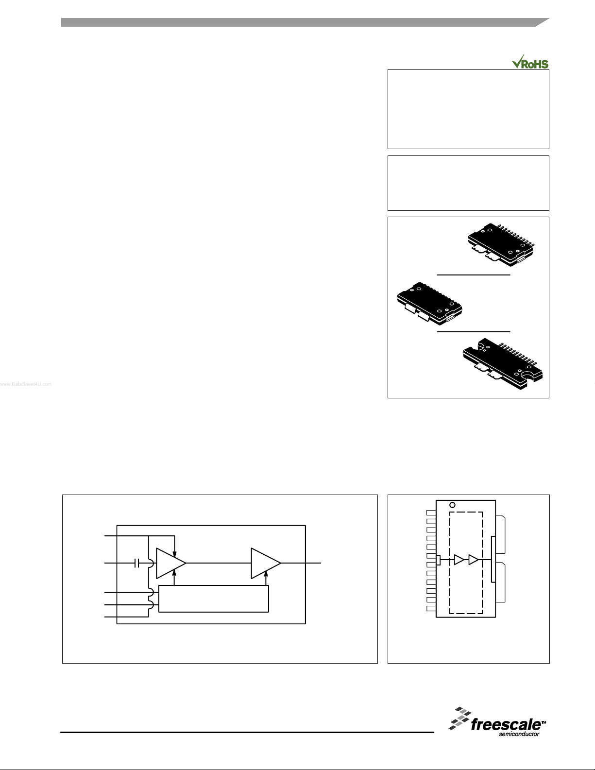
NC
1
V
DS1
V
DS1
RF
in
V
GS1
V
GS2
V
DS1
Quiescent Current
Temperature Compensation
(1)
RF
out/VDS2
RF
RF
V
GS1
V
GS2
V
DS1
Note: Exposed backside of the package is
Figure 1. Functional Block Diagram
1. Refer to AN1977, Quiescent Current Thermal Tracking Circuit in the RF Integrated Circuit Family and to AN1987, Quiescent Current Control
for the RF Integrated Circuit Device Family. Go to http://www.freescale.com/rf.
Select Documentation/Application Notes - AN1977 or AN1987.
Freescale Semiconductor, Inc., 2007. All rights reserved.
MWE6IC9100NR1 MWE6IC9100GNR1 MWE6IC9100NBR1
2
3
NC
NC
4
NC
5
6
in
7
in
8
NC
9
10
11
NC
12
(Top View)
the source terminal for the transistors.
14
13
RF
RF
/V
out
/V
out
Figure 2. Pin Connections
DS2
DS2
RF Device Data
Freescale Semiconductor
1
Page 2

Table 1. Maximum Ratings
Rating Symbol Value Unit
Drain-Source Voltage V
Gate- Source Voltage V
Storage Temperature Range T
Operating Junction Temperature T
Table 2. Thermal Characteristics
Characteristic Symbol Value
Thermal Resistance, Junction to Case
R
DSS
GS
stg
J
θ
JC
-0.5, +66 Vdc
-0.5, +6 Vdc
-65 to +200 °C
200 °C
(1,2)
Unit
°C/W
GSM Application Stage 1, 26 Vdc, I
(P
= 100 W CW) Stage 2, 26 Vdc, I
out
GSM EDGE Application Stage 1, 28 Vdc, I
(P
= 50 W Avg.) Stage 2, 28 Vdc, I
out
DQ1
DQ2
DQ1
DQ2
= 120 mA
= 950 mA
= 230 mA
= 870 mA
1.82
0.38
1.77
0.44
Table 3. ESD Protection Characteristics
Test Methodology Class
Human Body Model (per JESD22- A114) 2 (Minimum)
Machine Model (per EIA/JESD22-A115) B (Minimum)
Charge Device Model (per JESD22-C101) III (Minimum)
Table 4. Moisture Sensitivity Level
Test Methodology Rating Package Peak Temperature Unit
Per JESD 22-A113, IPC/JEDEC J-STD - 020 3 260 °C
Table 5. Electrical Characteristics (T
Characteristic Symbol Min Typ Max Unit
Stage 1 — Off Characteristics
Zero Gate Voltage Drain Leakage Current
(VDS = 66 Vdc, VGS = 0 Vdc)
Zero Gate Voltage Drain Leakage Current
(VDS = 28 Vdc, VGS = 0 Vdc)
Gate- Source Leakage Current
(VGS = 5 Vdc, VDS = 0 Vdc)
Stage 1 — On Characteristics
Gate Threshold Voltage
(VDS = 10 Vdc, ID = 35 µAdc)
Gate Quiescent Voltage
(VDS = 26 Vdc, ID = 120 mAdc)
Fixture Gate Quiescent Voltage
(VDD = 26 Vdc, ID = 120 mAdc, Measured in Functional Test)
1. Refer to AN1955, Thermal Measurement Methodology of RF Power Amplifiers. Go to http://www.freescale.com/rf.
Select Documentation/Application Notes - AN1955.
2. MTTF calculator available at http://www.freescale.com/rf. Select Tools/Software/Application Software/Calculators to access the MTTF
calculators by product.
= 25°C unless otherwise noted)
C
I
I
I
V
GS(th)
V
GS(Q)
V
GG(Q)
DSS
DSS
GSS
— — 10 µAdc
— — 1 µAdc
— — 10 µAdc
1.5 2 3.5 Vdc
— 2.7 — Vdc
6 9.4 12 Vdc
(continued)
MWE6IC9100NR1 MWE6IC9100GNR1 MWE6IC9100NBR1
2
RF Device Data
Freescale Semiconductor
Page 3

Table 5. Electrical Characteristics (T
= 25°C unless otherwise noted) (continued)
C
Characteristic Symbol Min Typ Max Unit
Stage 2 — Off Characteristics
Zero Gate Voltage Drain Leakage Current
I
DSS
— — 10 µAdc
(VDS = 66 Vdc, VGS = 0 Vdc)
Zero Gate Voltage Drain Leakage Current
(V
= 28 Vdc, VGS = 0 Vdc)
DS
Gate- Source Leakage Current
I
DSS
I
GSS
— — 1 µAdc
— — 10 µAdc
(VGS = 5 Vdc, VDS = 0 Vdc)
Stage 2 — On Characteristics
Gate Threshold Voltage
V
GS(th)
1.5 2 3.5 Vdc
(VDS = 10 Vdc, ID = 290 µAdc)
Gate Quiescent Voltage
V
GS(Q)
— 2.7 — Vdc
(VDS = 26 Vdc, ID = 950 mAdc)
Fixture Gate Quiescent Voltage
V
GG(Q)
6 8.6 12 Vdc
(VDD = 26 Vdc, ID = 950 mAdc, Measured in Functional Test)
Drain-Source On - Voltage
V
DS(on)
0.05 0.4 0.8 Vdc
(VGS = 10 Vdc, ID = 1 Adc)
Functional Tests (In Freescale Test Fixture, 50 ohm system) VDD = 26 Vdc, P
Power Gain G
= 100 W CW, I
out
ps
= 120 mA, I
DQ1
= 950 mA, f = 960 MHz
DQ2
31 33.5 36 dB
Input Return Loss IRL — -15 -10 dB
Power Added Efficiency PAE 52 54 — %
P
@ 1 dB Compression Point, CW P1dB 100 112 — W
out
Typical GSM EDGE Performances (In Freescale GSM EDGE Test Fixture, 50 ohm system) V
I
= 870 mA, 869 - 894 MHz and 920 - 960 MHz EDGE Modulation
DQ2
Power Gain G
ps
= 28 Vdc, P
DD
= 50 W Avg., I
out
— 35.5 — dB
DQ1
= 230 mA,
Power Added Efficiency PAE — 39 — %
Error Vector Magnitude EVM — 2 — % rms
Spectral Regrowth at 400 kHz Offset SR1 — -63 — dBc
Spectral Regrowth at 600 kHz Offset SR2 — -81 — dBc
RF Device Data
Freescale Semiconductor
MWE6IC9100NR1 MWE6IC9100GNR1 MWE6IC9100NBR1
3
Page 4
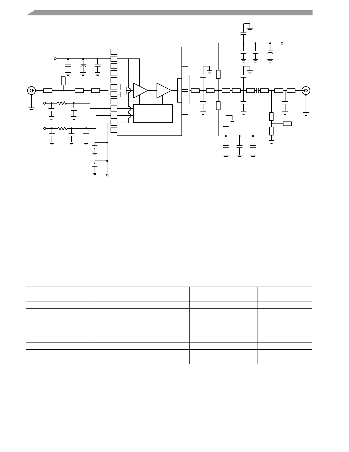
RF
INPUT
C8
1
C11
NC
2
3
NC
4
NC
NC
5
6
7
NC
8
9
10
11
12
NC
V
DD1
+
C17 C22
Z2
Z3
Z1
V
GG1
R1
C15
V
GG2
R2
Z4
C13
DUT
Quiescent Current
Temperature
Compensation
13
14
C1
Z5 Z6
C2
Z16
Z7 Z8 Z9
Z17
C9
C20
C7 C23
C3
C5
C4
+
Z10 Z15Z14
Z11
Z12
V
DD2
RF
OUTPUT
C6
Z13
C14C19C16
C12
C10 C24 C21
C18
V
DD1
Z1 0.089″ x 0.083″ Microstrip
Z2 0.157″ x 0.315″ Microstrip
Z3 0.157″ x 0.397″ Microstrip
Z4 0.139″ x 0.060″ Microstrip
Z5 0.024″ x 0.386″ Microstrip
Z6 0.352″ x 0.902″ Microstrip
Z7 0.039″ x 0.607″ Microstrip
Z8 0.555″ x 1.102″ Microstrip
Z10 1.117″ x 0.083″ Microstrip
Z11 0.067″ x 0.431″ Microstrip
Z12 0.067″ x 0.084″ Microstrip
Z13 0.381″ x 0.067″ Microstrip
Z14 0.418″ x 0.084″ Microstrip
Z15 0.421″ x 0.084″ Microstrip
Z16, Z17 2.550″ x 0.157″ Microstrip
PCB Taconic TLX8-0300, 0.030″, εr = 2.55
Z9 0.343″ x 0.083″ Microstrip
Figure 3. MWE6IC9100NR1(GNR1)(NBR1) Test Circuit Schematic
Table 6. MWE6IC9100NR1(GNR1)(NBR1) Test Circuit Component Designations and Values
Part Description Part Number Manufacturer
C1, C2 10 pF Chip Capacitors ATC100B100GT500XT ATC
C3, C4, C5 3.9 pF Chip Capacitors ATC100B3R9BT500XT ATC
C6 0.5 pF Chip Capacitor ATC100B0R5BT500XT AT C
C7, C8, C9, C10, C11, C12,
C13, C14
C15, C16, C17, C18, C19,
C20, C21
C22, C23 470 µF, 63 V Electrolytic Capacitors, Radial 222212018470 Vishay
C24 330 pF Chip Capacitor ATC100B331JT200XT ATC
R1, R2 4.7 kΩ, 1/8 W Chip Resistors WCR08054K7G Welwyn
33 pF Chip Capacitors ATC100B330JT500XT ATC
6.8 µF Chip Capacitors C4532X5R1H685MT TDK
MWE6IC9100NR1 MWE6IC9100GNR1 MWE6IC9100NBR1
4
RF Device Data
Freescale Semiconductor
Page 5
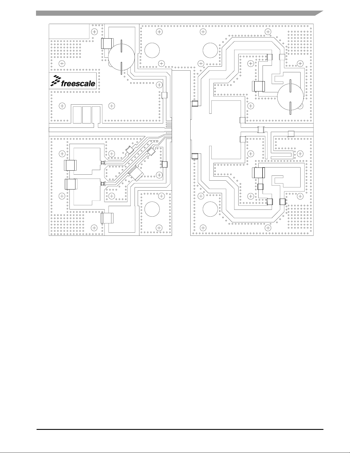
MWE6IC9100N
Rev. 4
C17
V
DD1
C7
C8
C15
C16
C22
V
DD2
C20
C11
C1
C23
C3
C5
C6
C4
C13
V
GG1
R1
C14
C12
C19
R2
V
GG2
C2
CUT OUT AREA
C21
C24
C10
C9
C18
Figure 4. MWE6IC9100NR1(GNR1)(NBR1) Test Circuit Component Layout
RF Device Data
Freescale Semiconductor
MWE6IC9100NR1 MWE6IC9100GNR1 MWE6IC9100NBR1
5
Page 6
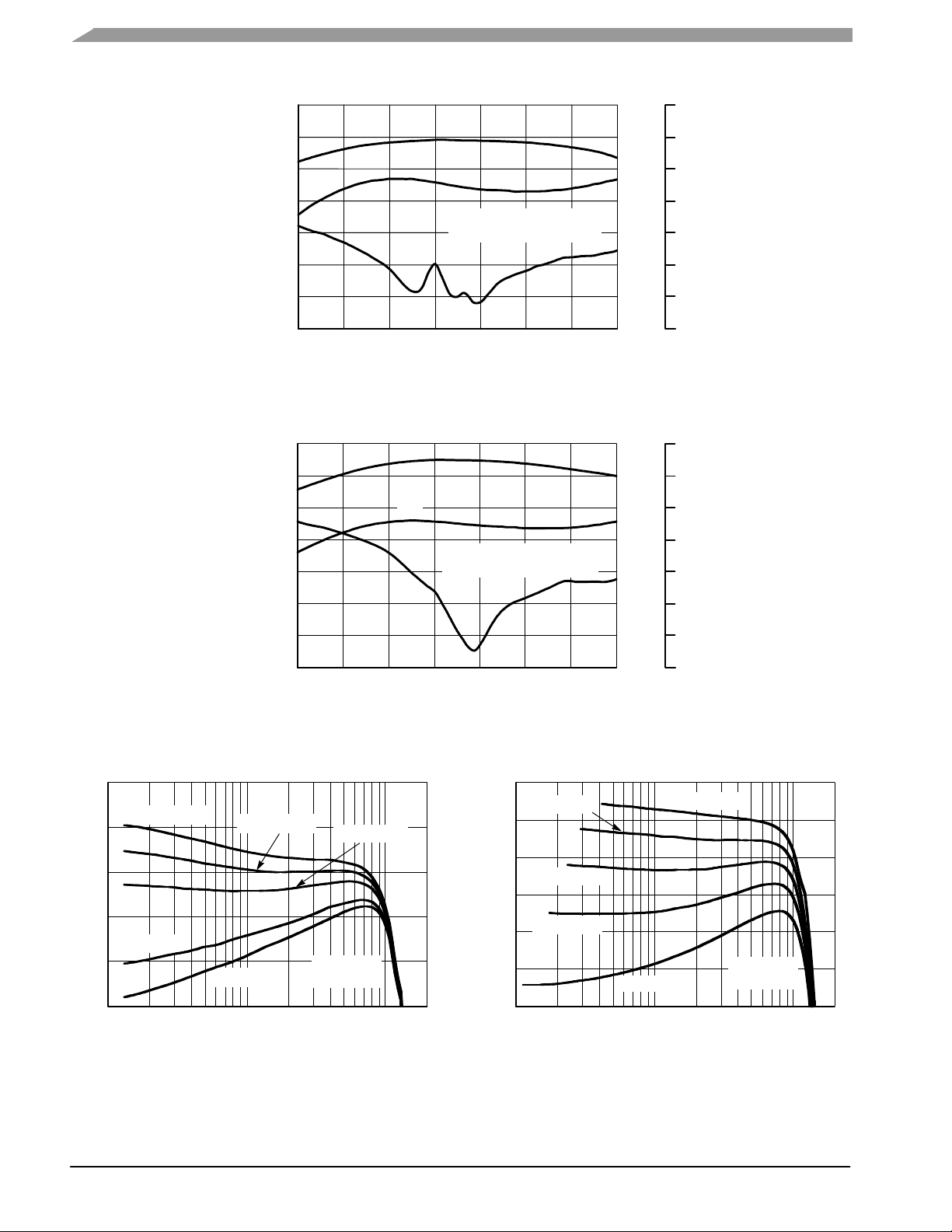
TYPICAL CHARACTERISTICS
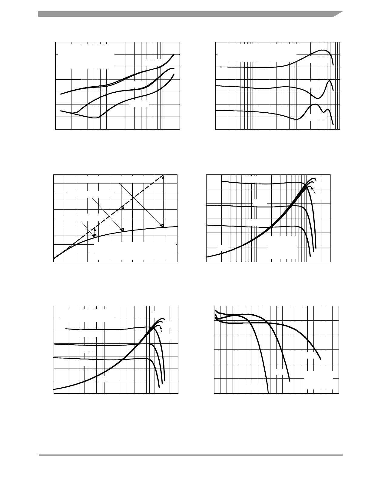
38 70
G
34
30
26
22
, POWER GAIN (dB)
ps
18
G
14
10
840
860 980900 920
IRL
880
ps
PAE
VDD = 26 Vdc, P
= 120 mA, I
I
DQ1
= 100 W CW
out
= 950 mA
DQ2
940 960
64
58
52
46
40
34
28
f, FREQUENCY (MHz)
Figure 5. Power Gain, Input Return Loss and Power Added
Efficiency versus Frequency @ P
38 52
34
30
26
22
, POWER GAIN (dB)
ps
18
G
14
10
840
G
ps
PAE
VDD = 28 Vdc, P
I
= 230 mA, I
DQ1
IRL
880
860 980900 920
f, FREQUENCY (MHz)
= 100 Watts CW
out
= 50 W Avg.
out
= 870 mA
DQ2
940 960
46
40
34
28
22
16
10
Figure 6. Power Gain, Input Return Loss and Power Added
Efficiency versus Frequency @ P
= 50 Watts Avg.
out
0
−4
−8
−12
−16
−20
IRL, INPUT RETURN LOSS (dB)
−24
PAE, POWER ADDED EFFICIENCY (%)
−28
−4
−8
−12
−16
−20
−24
IRL, INPUT RETURN LOSS (dB)
−28
PAE, POWER ADDED EFFICIENCY (%)
−30
36
I
= 1420 mA
DQ2
35
I
= 1190 mA
DQ2
I
DQ2
= 950 mA
34
33
, POWER GAIN (dB)
ps
I
G
= 590 mA
DQ2
32
I
= 470 mA
DQ2
VDD = 26 Vdc
f = 945 MHz
31
1
P
out
10 200
, OUTPUT POWER (WATTS) CW
100
Figure 7. Power Gain versus Output Power
@ I
= 120 mA
DQ1
MWE6IC9100NR1 MWE6IC9100GNR1 MWE6IC9100NBR1
6
36
I
= 180 mA
I
DQ1
= 150 mA
DQ1
35
34
I
= 120 mA
DQ1
33
I
= 90 mA
, POWER GAIN (dB)
ps
G
DQ1
32
31
I
= 60 mA
DQ1
30
1
P
out
10 200
, OUTPUT POWER (WATTS) CW
Figure 8. Power Gain versus Output Power
@ I
= 950 mA
DQ2
Freescale Semiconductor
VDD = 26 Vdc
f = 945 MHz
100
RF Device Data
Page 7
TYPICAL CHARACTERISTICS
,
(
)
−10
VDD = 26 Vdc
I
−20
= 120 mA, I
DQ1
f1 = 945 MHz, f2 = 945.1 MHz
100 kHz Tone Spacing
−30
= 950 mA
DQ2
3rd Order
−40
5th Order
−50
−60
7th Order
−70
IMD, INTERMODULATION DISTORTION (dBc)
−80
110
P
, OUTPUT POWER (WATTS) PEP
out
100
Figure 9. Intermodulation Distortion Products
versus Output Power
58
57
56
P3dB = 51.5 dBm (140 W)
55
54
P1dB = 50.9 dBm (123 W)
53
52
51
, OUTPUT POWER (dBc)
out
50
P
49
48
14 1715
16 18 19
P6dB = 51.95 dBm (156 W)
VDD = 26 Vdc, I
DQ1
Pulsed CW, 12 µsec(on), 1% Duty Cycle
f = 945 MHz
20 21 22 23 24
Pin, INPUT POWER (dBm)
Ideal
= 120 mA, I
= 950 mA
DQ2
Actual
Actual
Figure 11. Pulsed CW Output Power versus
Input Power
40
38
VDD = 26 Vdc, I
I
= 950 mA, f = 880 MHz
DQ2
DQ1
= 120 mA
−30_C
25_C
36
G
34
ps
TC = −30_C
85_C
25_C
32
, POWER GAIN (dB)
ps
30
G
28
85_C
PAE
26 0
101
P
, OUTPUT POWER (WATTS) CW
out
100
Figure 13. Power Gain and Power Added
Efficiency versus Output Power @ 880 MHz
−10
VDD = 26 Vdc, P
I
DQ2
−20
(f1 + f2)/2 = Center Frequency of 945 MHz
−30
−40
−50
−60
−70
IMD, INTERMODULATION DISTORTION (dBc)
−80
200
0.1 10
38
36
G
ps
34
32
30
, POWER GAIN (dB)
ps
G
28
PAE
26
25
Figure 12. Power Gain and Power Added
Efficiency versus Output Power @ 945 MHz
70
60
50
40
30
20
10
300
34
33
32
31
, POWER GAIN (dB)
30
ps
G
29
PAE, POWER ADDED EFFICIENCY (%)
28
0 150
Figure 14. Power Gain versus Output Power
= 100 W (PEP), I
= 1 A, Two− Tone Measurements
out
= 150 mA
DQ1
3rd Order
5th Order
7th Order
1
TWO−TONE SPACING (MHz)
Figure 10. Intermodulation Distortion
Products versus Tone Spacing
TC = −30_C
25_C
85_C
VDD = 26 Vdc
I
= 120 mA
DQ1
I
= 950 mA
DQ2
f = 945 MHz
101
P
, OUTPUT POWER (WATTS) CW
out
24 V
VDD = 20 V
50
P
, OUTPUT POWER (WATTS) CW
out
100
−30_C
25_C
85_C
100
32 V
I
= 120 mA
DQ1
I
= 950 mA
DQ2
f = 945 MHz
100
60
%
50
40
30
20
POWER ADDED EFFICIENCY
10
PAE
0
300
200
RF Device Data
Freescale Semiconductor
MWE6IC9100NR1 MWE6IC9100GNR1 MWE6IC9100NBR1
7
Page 8

TYPICAL CHARACTERISTICS
6
VDD = 28 Vdc
= 230 mA, I
I
DQ1
5
= 870 mA
DQ2
4
3
2
1
EVM, ERROR VECTOR MAGNITUDE (% ms)
0
880
Figure 15. EVM versus Frequency
−45
−50
−55
−60
TC = −30_C
−65
−70
−75
SPECTRAL REGROWTH @ 400 kHz (dBc)
−80
0
20
P
, OUTPUT POWER (WATTS)
out
Figure 17. Spectral Regrowth at 400 kHz
versus Output Power @ 945 MHz
P
= 63 W Avg.
out
55 W Avg.
25 W Avg.
960940920900
980
f, FREQUENCY (MHz)
85_C
25_C
VDD = 28 Vdc
I
= 230 mA, I
DQ1
= 870 mA
DQ2
f = 945 MHz, EDGE Modulation
40 120
60 80 100
−50
−55
SR @ 400 kHz
P
= 63 W Avg.
out
−60
55 W Avg.
−65
−70
−75
25 W Avg.
SR @ 600 kHz
25 W Avg.
VDD = 28 Vdc
= 230 mA, I
I
DQ1
f = 920 MHz, EDGE Modulation
−80
−85
860
SPECTRAL REGROWTH @ 400 kHz AND 600 kHz (dBc)
55 W Avg.
880 900 920 940 960
f, FREQUENCY (MHz)
Figure 16. Spectral Regrowth at 400 kHz and
600 kHz versus Frequency
−40
−45
−50
−55
−60
TC = −30_C
−65
−70
85_C
−75
SPECTRAL REGROWTH @ 400 kHz (dBc)
VDD = 28 Vdc
I
= 230 mA, I
DQ1
f = 880 MHz, EDGE Modulation
−80
0
20
40 60 80 100 120
P
, OUTPUT POWER (WATTS)
out
Figure 18. Spectral Regrowth at 400 kHz
versus Output Power @ 880 MHz
DQ2
DQ2
= 870 mA
63 W Avg.
980
25_C
= 870 mA
−60
VDD = 28 Vdc
I
−65
= 230 mA, I
DQ1
= 870 mA
DQ2
f = 945 MHz, EDGE Modulation
−70
−75
TC = −30_C
−80
−85
85_C
25_C
SPECTRAL REGROWTH @ 600 kHz (dBc)
−90
0
20
40 120
P
, OUTPUT POWER (WATTS)
out
60 80 100
Figure 19. Spectral Regrowth at 600 kHz
versus Output Power @ 945 MHz
MWE6IC9100NR1 MWE6IC9100GNR1 MWE6IC9100NBR1
8
−50
VDD = 28 Vdc
−55
I
= 230 mA, I
DQ1
DQ2
f = 880 MHz, EDGE Modulation
−60
−65
−70
−75
TC = −30_C
−80
SPECTRAL REGROWTH @ 600 kHz (dBc)
−85
0
20
P
, OUTPUT POWER (WATTS)
out
Figure 20. Spectral Regrowth at 600 kHz
versus Output Power @ 880 MHz
= 870 mA
25_C
85_C
40 60 80 100 120
RF Device Data
Freescale Semiconductor
Page 9

TYPICAL CHARACTERISTICS
10
VDD = 28 Vdc
I
= 230 mA
DQ1
8
= 870 mA
I
DQ2
f = 945 MHz
6
PAE
4
2
EVM, ERROR VECTOR MAGNITUDE (% ms)
0
TC = 25_C
101
P
, OUTPUT POWER (WATTS) AVG.
out
Figure 21. EVM and Power Added Efficiency
versus Output Power @ 945 MHz
10
VDD = 28 Vdc
I
= 230 mA
DQ1
I
= 870 mA
8
DQ2
f = 880 MHz
6
PAE
4
85_C
EVM
85_C
−30_C
50
40
30
20
10
PAE, POWER ADDED EFFICIENCY (%)
0
100
50
40
30
20
2
EVM, ERROR VECTOR MAGNITUDE (% ms)
0
Figure 22. EVM and Power Added Efficiency
40
S21
30
20
S21 (dB)
10
S11
0
VDD = 26 Vdc
−10
= 120 mA, I
DQ1
= 950 mA
DQ2
I
400
f, FREQUENCY (MHz)
Figure 23. Broadband Frequency Response
25_C
TC = −30_C
101
P
, OUTPUT POWER (WATTS) AVG.
out
versus Output Power @ 880 MHz
0
−5
−10
−15
−20
−25
140012001000800600
1600
38
36
34
32
S11 (dB)
, POWER GAIN (dB)
30
ps
G
28
26
820
Figure 24. Power Gain versus Frequency
10
EVM
PAE, POWER ADDED EFFICIENCY (%)
0
100
TC = −30_C
25_C
85_C
VDD = 26 Vdc, P
I
= 120 mA, I
DQ1
860 900 940
840 880 920 960
= 60 W CW
out
= 950 mA
DQ2
f, FREQUENCY (MHz)
980
RF Device Data
Freescale Semiconductor
MWE6IC9100NR1 MWE6IC9100GNR1 MWE6IC9100NBR1
9
Page 10

TYPICAL CHARACTERISTICS
8
10
7
10
6
10
1st Stage
MTTF (HOURS)
5
10
4
10
90
110 130 150 170 190
TJ, JUNCTION TEMPERATURE (°C)
This above graph displays calculated MTTF in hours when the device
is operated at VDD = 26 Vdc, P
MTTF calculator available at http:/www.freescale.com/rf. Select Tools/
Software/Application Software/Calculators to access the MTTF calcu−
lators by product.
= 100 W CW, and PAE = 54%.
out
Figure 25. MTTF versus Junction Temperature
210 230
2nd Stage
250
(dB)
−100
−110
−10
−20
−30
−40
−50
−60
−70
−80
−90
Reference Power
400 kHz
600 kHz
GSM TEST SIGNAL
VWB = 30 kHz
Sweep Time = 70 ms
RBW = 30 kHz
400 kHz
600 kHz
200 kHz Span 2 MHzCenter 1.96 GHz
Figure 26. EDGE Spectrum
MWE6IC9100NR1 MWE6IC9100GNR1 MWE6IC9100NBR1
10
RF Device Data
Freescale Semiconductor
Page 11

f = 980 MHz
f = 820 MHz
Zo = 50 Ω
f = 820 MHz
Z
source
f = 980 MHz
Z
load
VDD = 26 Vdc, I
f
MHz
= 120 mA, I
DQ1
Z
source
W
= 950 mA, P
DQ2
820 35.40 + j21.50 0.516 - j0.365
840 35.00 + j18.00 0.638 - j0.172
860 35.00 + j15.50 0.768 - j0.010
880 34.50 + j12.20 0.874 + j0.071
900 34.00 + j9.00 1.030 + j0.133
920 34.30 + j7.20 1.101 + j0.082
940 38.50 + j6.00 1.088 + j0.037
960 42.00 + j7.40 1.011 + j0.018
980 45.55 + j12.75 0.872 + j0.051
Z
= Test circuit impedance as measured from
source
Z
load
gate to ground.
= Test circuit impedance as measured
from drain to ground.
Input
Matching
Network
Device
Under
Test
= 100 W CW
out
Z
load
W
Output
Matching
Network
RF Device Data
Freescale Semiconductor
Z
source
Z
load
Figure 27. Series Equivalent Source and Load Impedance
MWE6IC9100NR1 MWE6IC9100GNR1 MWE6IC9100NBR1
11
Page 12

Table 7. Common Source Scattering Parameters (V
f
S
11
MHz
|S11| ∠φ |S21| ∠φ |S12| ∠φ |S22| ∠φ
= 26 V, 50 ohm system, I
DD
S
21
S
DQ1
12
= 120 mA, I
= 950 mA)
DQ2
750 0.230 95 5.81 -87 0.0007 -119 0.989 - 180
760 0.188 93 6.48 -97 0.0007 -116 0.987 180
770 0.149 92 7.18 -107 0.0007 -111 0.985 180
780 0.114 92 7.88 -117 0.0007 -110 0.983 180
790 0.085 96 8.56 -128 0.0008 -109 0.981 180
800 0.063 104 9.22 - 139 0.0008 - 108 0.979 180
810 0.047 11 7 9.82 -150 0.0009 -109 0.978 180
820 0.037 134 10.37 - 161 0.0009 -110 0.978 - 180
830 0.031 156 10.85 - 172 0.0009 -111 0.977 - 180
840 0.029 - 177 11.27 178 0.0010 -113 0.977 - 180
850 0.033 - 152 11.60 167 0.0010 -114 0.978 - 180
860 0.041 - 134 11.87 156 0.0010 -117 0.978 - 180
870 0.052 - 123 12.07 146 0.0010 -119 0.979 -180
880 0.063 -116 12.20 135 0.0010 - 122 0.979 -180
890 0.074 -112 12.25 125 0.0010 - 123 0.979 180
900 0.084 - 109 12.23 115 0.0010 -126 0.980 180
910 0.094 - 106 12.15 106 0.0010 -129 0.979 180
920 0.104 - 103 12.01 96 0.0010 - 131 0.978 180
930 0.113 -99 11.82 86 0.0009 - 133 0.978 180
940 0.125 -95 11.57 77 0.0009 - 135 0.977 180
950 0.141 -91 11.28 68 0.0008 - 138 0.976 180
960 0.160 -88 10.97 59 0.0008 - 136 0.976 180
970 0.183 -86 10.62 50 0.0007 - 135 0.976 180
980 0.209 -85 10.23 42 0.0006 - 133 0.976 180
990 0.238 -85 9.83 34 0.0006 -130 0.975 180
1000 0.268 -86 9.41 26 0.0006 -125 0.975 180
S
22
MWE6IC9100NR1 MWE6IC9100GNR1 MWE6IC9100NBR1
12
RF Device Data
Freescale Semiconductor
Page 13

PACKAGE DIMENSIONS
RF Device Data
Freescale Semiconductor
MWE6IC9100NR1 MWE6IC9100GNR1 MWE6IC9100NBR1
13
Page 14

MWE6IC9100NR1 MWE6IC9100GNR1 MWE6IC9100NBR1
14
RF Device Data
Freescale Semiconductor
Page 15

RF Device Data
Freescale Semiconductor
MWE6IC9100NR1 MWE6IC9100GNR1 MWE6IC9100NBR1
15
Page 16

MWE6IC9100NR1 MWE6IC9100GNR1 MWE6IC9100NBR1
16
RF Device Data
Freescale Semiconductor
Page 17

RF Device Data
Freescale Semiconductor
MWE6IC9100NR1 MWE6IC9100GNR1 MWE6IC9100NBR1
17
Page 18

MWE6IC9100NR1 MWE6IC9100GNR1 MWE6IC9100NBR1
18
RF Device Data
Freescale Semiconductor
Page 19

RF Device Data
Freescale Semiconductor
MWE6IC9100NR1 MWE6IC9100GNR1 MWE6IC9100NBR1
19
Page 20

MWE6IC9100NR1 MWE6IC9100GNR1 MWE6IC9100NBR1
20
RF Device Data
Freescale Semiconductor
Page 21

RF Device Data
Freescale Semiconductor
MWE6IC9100NR1 MWE6IC9100GNR1 MWE6IC9100NBR1
21
Page 22

PRODUCT DOCUMENTATION
Refer to the following documents to aid your design process.
Application Notes
• AN1907: Solder Reflow Attach Method for High Power RF Devices in Plastic Packages
• AN1949: Mounting Method for the MHVIC910HR2 (PFP- 16) and Similar Surface Mount Packages
• AN1955: Thermal Measurement Methodology of RF Power Amplifiers
• AN3263: Bolt Down Mounting Method for High Power RF Transistors and RFICs in Over- Molded Plastic Packages
Engineering Bulletins
• EB212: Using Data Sheet Impedances for RF LDMOS Devices
REVISION HISTORY
The following table summarizes revisions to this document.
Revision Date Description
0 Feb. 2007 • Initial Release of Data Sheet
1 May 2007 • Changed Device box to 960 MHz to reflect functional test frequency, p. 1
• Added Power Added Efficiency to GSM EDGE Application Typical Performances, p. 1
• Changed “5:1 VSWR, @ 28 Vdc” to “10:1 VSWR, @ 32 Vdc” in the Capable of Handling bullet, p. 1
• Added Footnote (1) to Quiescent Current Thermal Tracking bullet under Features section and to
Quiescent Current Temperature Compensation in Fig. 1, Functional Block Diagram, p. 1
• Added top - level, 2 -stage block diagram depiction to Fig. 2, Pin Connections; updated Note, p. 1
• Added Case Operating Temperature limit to the Maximum Ratings table and set limit to 150°C, p. 2
• Added Stage 1 and Stage 2 DC Electrical Characteristics tables, p. 2, 3
• In Table 6, Component Designations and Values, corrected Part Number ATC100B331JT500XT to
ATC100B331JT200XT for C24 capacitor, p. 4
• Updated Figs. 7 and 8, Power Gain versus Output Power, to remove non-variable IDQ value, p. 6
• Updated Fig. 9, Intermodulation Distortion Products versus Output Power, to show PEP and not CW;
corrected frequency value to show 100 kHz Tone Spacing, p. 7
• Updated graphical representation of Ideal/Actual in Fig. 11, Pulsed CW Output Power versus Input Power,
to show correct 3 and 6 dB compression points, p. 7
2 June 2007 • Removed Case Operating Temperature from Maximum Ratings table, p. 2. Case Operating Temperature
rating will be added to the Maximum Ratings table when parts’ Operating Junction Temperature is
increased to 225°C.
MWE6IC9100NR1 MWE6IC9100GNR1 MWE6IC9100NBR1
22
RF Device Data
Freescale Semiconductor
Page 23

How to Reach Us:
Home Page:
www.freescale.com
Web Support:
http://www.freescale.com/support
USA/Europe or Locations Not Listed:
Freescale Semiconductor, Inc.
Technical Information Center, EL516
2100 East Elliot Road
Tempe, Arizona 85284
+1-800 - 521 - 6274 or +1 - 480- 768- 2130
www.freescale.com/support
Europe, Middle East, and Africa:
Freescale Halbleiter Deutschland GmbH
Technical Information Center
Schatzbogen 7
81829 Muenchen, Germany
+44 1296 380 456 (English)
+46 8 52200080 (English)
+49 89 92103 559 (German)
+33 1 69 35 48 48 (French)
www.freescale.com/support
Japan:
Freescale Semiconductor Japan Ltd.
Headquarters
ARCO Tower 15F
1-8 - 1, Shimo - Meguro, Meguro - ku,
Tokyo 153-0064
Japan
0120 191014 or +81 3 5437 9125
support.japan@freescale.com
Asia/Pacific:
Freescale Semiconductor Hong Kong Ltd.
Technical Information Center
2 Dai King Street
Tai Po Industrial Estate
Tai Po, N.T., Hong Kong
+800 2666 8080
support.asia@freescale.com
For Literature Requests Only:
Freescale Semiconductor Literature Distribution Center
P.O. Box 5405
Denver, Colorado 80217
1-800 - 441 - 2447 or 303 - 675- 2140
Fax: 303-675 - 2150
LDCForFreescaleSemiconductor@hibbertgroup.com
Information in this document is provided solely to enable system and software
implementers to use Freescale Semiconductor products. There are no express or
implied copyright licenses granted hereunder to design or fabricate any integrated
circuits or integrated circuits based on the information in this document.
Freescale Semiconductor reserves the right to make changes without further notice to
any products herein. Freescale Semiconductor makes no warranty, representation or
guarantee regarding the suitability of its products for any particular purpose, nor does
Freescale Semiconductor assume any liability arising out of the application or use of
any product or circuit, and specifically disclaims any and all liability, including without
limitation consequential or incidental damages. “Typical” parameters that may be
provided in Freescale Semiconductor data sheets and/or specifications can and do
vary in different applications and actual performance may vary over time. All operating
parameters, including “Typicals”, must be validated for each customer application by
customer’s technical experts. Freescale Semiconductor does not convey any license
under its patent rights nor the rights of others. Freescale Semiconductor products are
not designed, intended, or authorized for use as components in systems intended for
surgical implant into the body, or other applications intended to support or sustain life,
or for any other application in which the failure of the Freescale Semiconductor product
could create a situation where personal injury or death may occur. Should Buyer
purchase or use Freescale Semiconductor products for any such unintended or
unauthorized application, Buyer shall indemnify and hold Freescale Semiconductor
and its officers, employees, subsidiaries, affiliates, and distributors harmless against all
claims, costs, damages, and expenses, and reasonable attorney fees arising out of,
directly or indirectly, any claim of personal injury or death associated with such
unintended or unauthorized use, even if such claim alleges that Freescale
Semiconductor was negligent regarding the design or manufacture of the part.
Freescalet and the Freescale logo are trademarks of Freescale Semiconductor, Inc.
All other product or service names are the property of their respective owners.
Freescale Semiconductor, Inc. 2007. All rights reserved.
Document Number: MWE6IC9100N
RF Device Data
Rev. 2, 6/2007
Freescale Semiconductor
MWE6IC9100NR1 MWE6IC9100GNR1 MWE6IC9100NBR1
23
 Loading...