

Page 1
C
O
O
Freescale Semiconductor
Technical Data
MRFG35010NT1 replaced by MRFG35010ANT1.
Document Number: MRFG35010N
Rev. 7, 1/2008
Gallium Arsenide PHEMT
RF Power Field Effect Transistor
Designed for WLL/MMDS/BWA or UMTS driver applications with frequencies
from 1.8 to 3.6 GHz. This device is unmatched and is suitable for use in Class
AB linear base station applications.
• Typical W-CDMA Performance: - 42 dBc ACPR, 3.55 GHz, 12 Volts,
IDQ = 180 mA, 5 MHz Offset/3.84 MHz BW, 64 DPCH (8.5 dB P/A
@ 0.01% Probability)
Output Power — 900 mW
Power Gain — 10 dB
N
Efficiency — 28%
• 9 Watts P1dB @ 3.55 GHz
• Excellent Phase Linearity and Group Delay Characteristics
• High Gain, High Efficiency and High Linearity
• N Suffix Indicates Lead- Free Terminations. RoHS Compliant.
• In Tape and Reel. T1 Suffix = 1000 Units per 12 mm, 7 inch Reel.
RMATI
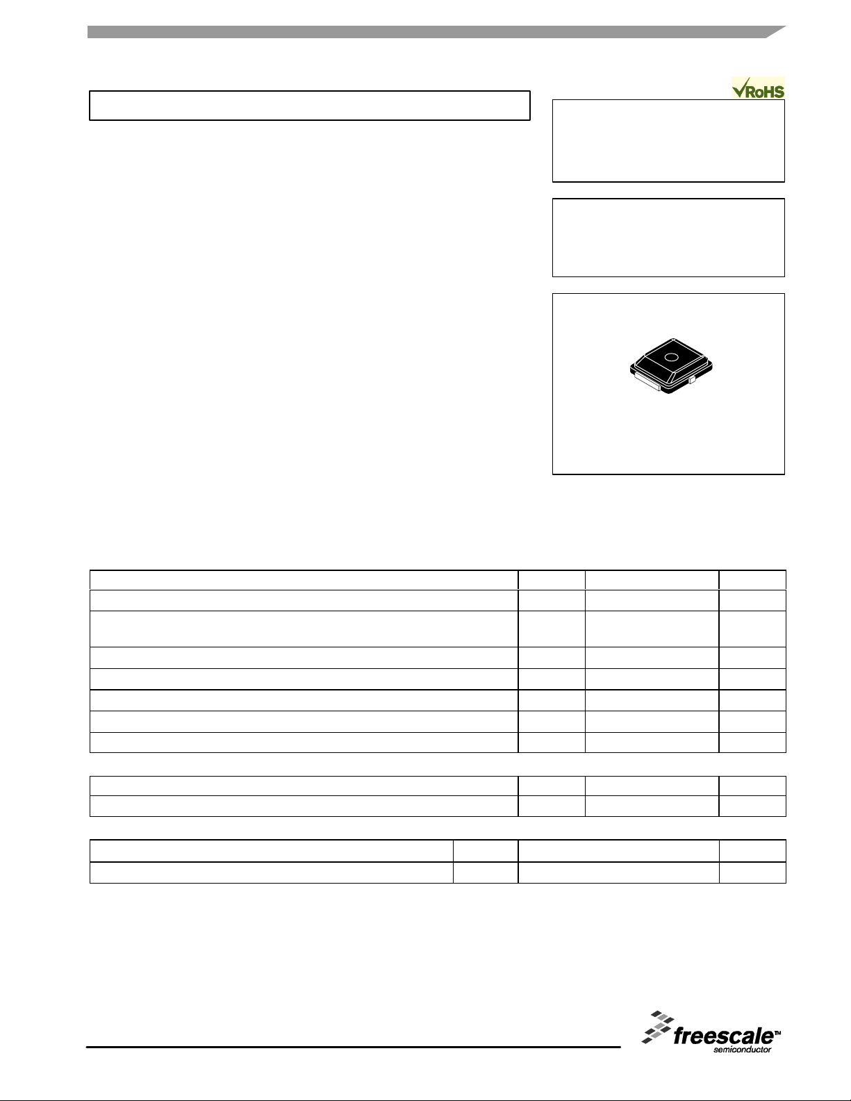
MRFG35010NT1
3.5 GHz, 9 W, 12 V
POWER FET
GaAs PHEMT
CASE 466-03, STYLE 1
PLD-1.5
PLASTIC
Table 1. Maximum Ratings
Rating Symbol Value Unit
Drain-Source Voltage V
Total Device Dissipation @ TC = 25°C
Derate above 25°C
Gate- Source Voltage V
RF Input Power P
HIVE INF
Storage Temperature Range T
Channel Temperature
Operating Case Temperature Range T
Table 2. Thermal Characteristics
AR
Thermal Resistance, Junction to Case R
Table 3. Moisture Sensitivity Level
Per JESD 22-A113, IPC/JEDEC J-STD - 020 1 260 °C
1. For reliable operation, the operating channel temperature should not exceed 150°C.
2. Simulated.
(1)
Characteristic Symbol Value Unit
Test Methodology Rating Package Peak Temperature Unit
DSS
P
GS
stg
T
ch
θ
D
in
C
JC
15 Vdc
(2)
22.7
(2)
0.15
-5 Vdc
33 dBm
-65 to +150 °C
175 °C
-20 to +85 °C
(2)
6.6
W
W/°C
ARCHIVE INFORMATION
°C/W
Freescale Semiconductor, Inc., 2006, 2008. All rights reserved.
RF Device Data
Freescale Semiconductor
MRFG35010NT1
1
Page 2
C
O
O
Table 4. Electrical Characteristics
Characteristic Symbol Min Typ Max Unit
Saturated Drain Current
(VDS = 3.5 Vdc, VGS = 0 Vdc)
Off State Leakage Current
(VGS = - 0.4 Vdc, VDS = 0 Vdc)
Off State Drain Current
(VDS = 12 Vdc, VGS = -1.9 Vdc)
Off State Current
(VDS = 28.5 Vdc, VGS = -2.5 Vdc)
Gate- Source Cut - off Voltage
(VDS = 3.5 Vdc, IDS = 15 mA)
Quiescent Gate Voltage
(VDS = 12 Vdc, IDQ = 180 mA)
Power Gain
(VDD = 12 Vdc, IDQ = 180 mA, f = 3.55 GHz)
N
Output Power, 1 dB Compression Point
(VDD = 12 Vdc, IDQ = 180 mA, f = 3.55 GHz)
Drain Efficiency
(VDD = 12 Vdc, IDQ = 180 mA, P
f = 3.55 GHz)
Adjacent Channel Power Ratio
(VDD = 12 Vdc, P
f = 3.55 GHz, W- CDMA, 8.5 P/A @ 0.01% Probability,
64 CH, 3.84 MCPS)
RMATI
= 900 mW Avg., IDQ = 180 mA,
out
(TC = 25°C unless otherwise noted)
= 900 mW Avg.,
out
I
DSS
I
GSS
I
DSO
I
DSX
V
GS(th)
V
GS(Q)
G
ps
P1dB — 9 — W
h
D
ACPR — -43 -40 dBc
— 2.9 — Adc
— < 1.0 100 µAdc
— 0.1 1.0 mAdc
— 2.0 15 mAdc
-1.2 -1.0 - 0.7 Vdc
-1.2 -0.95 -0.7 Vdc
9.0 10 — dB
23 28 — %
HIVE INF
AR
MRFG35010NT1
2
ARCHIVE INFORMATION
RF Device Data
Freescale Semiconductor
Page 3
C
O
O
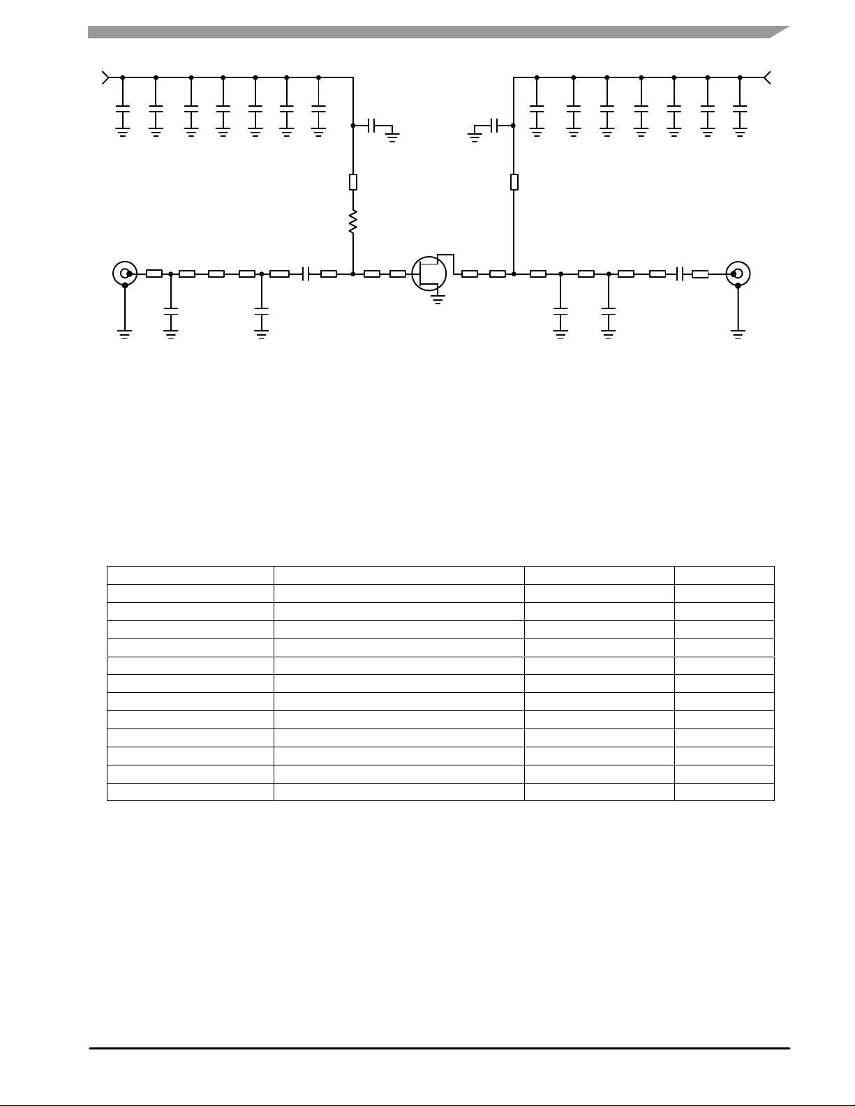
V
BIAS
C11
C10 C9 C8 C7 C6 C5 C18 C17 C16 C15 C14 C13 C12
C4
C19
V
SUPPLY
Z9
RF
INPUT
Z1 Z2 Z3 Z5 Z6 Z7 Z10 Z11 Z13 Z14 Z17
C1
Z4
C3
C2
R1
Z8
Z12
Z15 Z16
C22 C21
N
Z1 0.045″ x 0.689″ Microstrip
Z2 0.045″ x 0.089″ Microstrip
Z3 0.020″ x 0.360″ Microstrip
Z4 0.045″ x 0.029″ Microstrip
Z5 0.045″ x 0.061″ Microstrip
Z6 0.045″ x 0.055″ Microstrip
Z7 0.300″ x 0.125″ Microstrip
Z8, Z10 0.146″ x 0.070″ Microstrip
Z9 0.025″ x 0.485″ Microstrip
Z11 0.400″ x 0.215″ Microstrip
Z12 0.025″ x 0.497″ Microstrip
Z13 0.025″ x 0.271″ Microstrip
Z14 0.025″ x 0.363″ Microstrip
Z15 0.025″ x 0.041″ Microstrip
Z16 0.045″ x 0.050″ Microstrip
Z17 0.045″ x 0.467″ Microstrip
PCB Rogers 4350, 0.020″, εr = 3.5
RMATI
Figure 1. 3.5 GHz Test Circuit Schematic
Table 5. 3.5 GHz Test Circuit Component Designations and Values
Part Description Part Number Manufacturer
C1, C21, C22 0.5 pF Chip Capacitors 08051J0R5BBT AVX
C2 0.2 pF Chip Capacitor 06035J0R2BBT AVX
C3 0.5 pF Chip Capacitor 06035J0R5BBT AVX
C4, C19, C20 6.8 pF Chip Capacitors 08051J6R8BBT AVX
C5, C18 10 pF Chip Capacitors 100A100JP150X ATC
C6, C17 100 pF Chip Capacitors 100A101JP150X ATC
HIVE INF
C7, C16 100 pF Chip Capacitors 100B101JP500X ATC
C8, C15 1000 pF Chip Capacitors 100B102JP50X ATC
C9, C14 0.1 µF Chip Capacitors CDR33BX104AKWS Kemet
C10, C13 39K pF Chip Capacitors 200B393KP50X ATC
AR
C11, C12 10 µF Chip Capacitors GRM55DR61H106KA88B Kemet
R1 47 Ω Chip Resistor D55342M07B47JOR Newark
RF
OUTPUT
C20
ARCHIVE INFORMATION
RF Device Data
Freescale Semiconductor
MRFG35010NT1
3
Page 4

C
O
O
C11
C10 C9
C14 C13
C12
N
RMATI
C1
C4
C6
C5
C2
C8
C7
C3
C15
C16
C17
C18
C19
R1
C20
C22 C21
MRFG35010XX, Rev. 5
HIVE INF
AR
MRFG35010NT1
4
Figure 2. 3.5 GHz Test Circuit Component Layout
ARCHIVE INFORMATION
RF Device Data
Freescale Semiconductor
Page 5

C
O
O
TYPICAL CHARACTERISTICS
N
RMATI
0
IRL
−10 −10
VDS = 12 Vdc, IDQ = 180 mA
−20
f = 3.55 GHz, 8.66 P/A 3GPP W−CDMA
Γ
= 0.898é−134.03_, ΓL = 0.828é−140.67_
S
−30 −30
−40
INPUT RETURN LOSS (dB)IRL,
ACPR
−50 −50
−60
0.1
P
, OUTPUT POWER (WATTS)
out
Figure 3. W- CDMA ACPR and Input Return
Loss versus Output Power
12.5
VDS = 12 Vdc, IDQ = 180 mA
12
11.5
11
10.5
, TRANSDUCER GAIN (dB)
T
G
10
f = 3.55 GHz, 8.5 P/A 3GPP W−CDMA
ΓS = 0.898é−134.03_, ΓL = 0.828é−140.67_
G
T
1
PAE
10
0
−20
−40
−60
60
50
40
30
20
10
ACPR (dBc)
, POWER ADDED EFFICIENCY (%)PAE
HIVE INF
NOTE: All data is referenced to package lead interface. ΓS and Γ
All data is generated from load pull, not from the test circuit shown.
AR
9.5
0.1
P
, OUTPUT POWER (WATTS)
out
Figure 4. Transducer Gain and Power Added
Efficiency versus Output Power
1
are the impedances presented to the DUT.
L
0
10
ARCHIVE INFORMATION
RF Device Data
Freescale Semiconductor
MRFG35010NT1
5
Page 6

C
O
O
Table 6. Class AB Common Source S - Parameters at V
f
S
11
GHz
0.5 0.946 - 177.11 4.710 82.28 0.016 8.19 0.759 - 179.39
0.55 0.945 - 178.28 4.303 80.79 0.016 7.57 0.758 - 179.99
0.6 0.944 -179.44 3.963 79.23 0.016 7.60 0.758 179.39
0.65 0.945 179.50 3.674 77.69 0.016 7.44 0.758 178.74
0.7 0.945 178.60 3.427 76.28 0.016 7.44 0.757 177.98
0.75 0.944 177.66 3.211 74.83 0.016 7.21 0.757 177.28
0.8 0.945 176.74 3.023 73.24 0.017 7.65 0.756 176.57
0.85 0.945 175.95 2.853 71.74 0.017 7.16 0.756 175.75
0.9 0.944 175.17 2.705 70.36 0.017 7.34 0.756 174.99
0.95 0.945 174.36 2.570 68.88 0.017 7.31 0.755 174.18
1 0.945 173.63 2.447 67.47 0.017 7.08 0.755 173.33
1.05 0.944 172.90 2.337 66.06 0.017 7.29 0.756 172.51
N
1.1 0.944 172.09 2.234 64.52 0.017 7.56 0.756 171.82
1.15 0.944 171.29 2.139 63.11 0.017 7.46 0.756 171.01
1.2 0.944 170.57 2.052 61.73 0.017 7.43 0.757 170.22
1.25 0.943 169.71 1.971 60.26 0.017 7.47 0.757 169.52
1.3 0.944 168.85 1.894 58.81 0.017 7.28 0.757 168.83
1.35 0.940 168.20 1.823 57.49 0.017 7.56 0.755 168.39
1.4 0.946 167.07 1.754 56.13 0.017 7.92 0.762 167.55
1.45 0.943 166.35 1.691 54.75 0.018 7.59 0.759 167.32
RMATI
1.5 0.944 163.30 1.626 53.36 0.017 7.06 0.762 169.20
1.55 0.943 162.54 1.573 52.16 0.017 7.24 0.763 168.75
1.6 0.942 161.81 1.523 50.87 0.017 7.48 0.764 168.22
1.65 0.945 161.17 1.474 49.56 0.018 7.46 0.765 167.71
1.7 0.946 160.55 1.429 48.35 0.017 7.46 0.766 167.18
1.75 0.945 160.01 1.387 47.14 0.018 7.84 0.767 166.73
1.8 0.945 159.48 1.348 45.88 0.018 7.89 0.767 166.15
1.85 0.947 159.00 1.310 44.70 0.018 7.97 0.768 165.58
1.9 0.946 158.52 1.274 43.55 0.018 7.87 0.770 165.10
1.95 0.945 158.06 1.240 42.30 0.018 7.89 0.769 164.54
HIVE INF
AR
2 0.948 157.71 1.209 41.23 0.018 7.61 0.771 164.05
2.05 0.947 157.30 1.179 40.16 0.018 7.78 0.772 163.59
2.1 0.947 156.92 1.152 39.09 0.018 7.65 0.773 163.12
2.15 0.948 156.58 1.127 37.97 0.018 7.40 0.773 162.56
2.2 0.948 156.32 1.102 36.90 0.019 7.22 0.773 162.01
2.25 0.948 156.04 1.079 35.82 0.019 6.98 0.775 161.53
2.3 0.949 155.73 1.058 34.70 0.019 7.24 0.775 161.05
2.35 0.949 155.33 1.037 33.62 0.019 7.52 0.775 160.43
2.4 0.948 154.99 1.019 32.54 0.019 7.60 0.776 159.99
2.45 0.948 154.57 1.002 31.44 0.019 7.49 0.777 159.53
2.5 0.948 154.13 0.986 30.35 0.019 7.69 0.776 158.91
2.55 0.946 153.68 0.971 29.28 0.019 8.05 0.777 158.40
2.6 0.946 153.15 0.957 28.12 0.020 8.01 0.777 157.88
2.65 0.946 152.54 0.943 26.91 0.020 8.01 0.776 157.34
2.7 0.945 151.98 0.930 25.73 0.020 7.82 0.777 156.80
2.75 0.943 151.22 0.918 24.52 0.021 7.27 0.778 156.36
|S11| ∠φ |S21| ∠φ |S12| ∠φ |S22| ∠φ
= 12 Vdc, IDQ = 180 mA
DS
S
21
S
12
S
22
ARCHIVE INFORMATION
MRFG35010NT1
6
RF Device Data
Freescale Semiconductor
Page 7

C
O
O
f
Table 6. Class AB Common Source S - Parameters at VDS = 12 Vdc, IDQ = 180 mA (continued)
S
11
GHz
2.8 0.943 150.66 0.906 23.27 0.021 6.42 0.776 155.80
2.85 0.943 149.88 0.894 22.02 0.022 5.21 0.777 155.28
2.9 0.942 149.16 0.883 20.80 0.021 4.17 0.778 154.81
2.95 0.942 148.32 0.872 19.56 0.021 4.03 0.778 154.25
3 0.943 147.41 0.862 18.28 0.021 3.53 0.778 153.67
3.05 0.942 146.51 0.853 16.96 0.022 3.11 0.780 153.18
3.1 0.940 145.45 0.842 15.64 0.022 2.65 0.780 152.64
3.15 0.940 144.41 0.833 14.29 0.022 2.43 0.779 152.04
3.2 0.941 143.33 0.823 13.00 0.022 2.48 0.782 151.43
3.25 0.938 142.25 0.814 11.67 0.022 2.48 0.781 150.92
3.3 0.939 141.15 0.804 10.32 0.022 2.08 0.781 150.33
3.35 0.939 140.02 0.795 8.97 0.022 1.99 0.782 149.74
N
3.4 0.938 138.89 0.785 7.61 0.022 2.11 0.783 149.19
3.45 0.938 137.88 0.776 6.26 0.023 2.05 0.782 148.72
3.5 0.939 136.68 0.767 4.96 0.023 1.79 0.783 147.97
3.55 0.938 135.63 0.757 3.67 0.023 1.56 0.785 147.40
3.6 0.938 134.63 0.748 2.34 0.024 1.02 0.783 146.88
3.65 0.939 133.60 0.739 1.04 0.024 0.44 0.783 146.20
3.7 0.938 132.68 0.729 - 0.25 0.024 -0.54 0.785 145.61
3.75 0.937 131.84 0.720 -1.47 0.024 - 1.30 0.785 145.17
RMATI
3.8 0.937 130.92 0.711 - 2.69 0.024 - 1.98 0.785 144.52
3.85 0.938 130.07 0.702 -3.89 0.024 - 2.38 0.786 143.87
3.9 0.938 129.29 0.694 - 5.07 0.024 -2.22 0.787 143.24
3.95 0.939 128.60 0.686 -6.23 0.024 - 2.00 0.787 142.61
4 0.939 127.88 0.678 -7.34 0.025 - 1.80 0.788 141.94
4.05 0.939 127.23 0.671 - 8.46 0.025 - 2.04 0.789 141.34
4.1 0.941 126.66 0.664 - 9.57 0.025 -2.17 0.789 140.69
4.15 0.941 126.23 0.658 -10.65 0.025 - 2.15 0.788 140.01
4.2 0.940 125.73 0.651 -11.72 0.026 - 2.48 0.789 139.31
4.25 0.939 125.28 0.645 -12.82 0.026 - 2.81 0.789 138.65
HIVE INF
4.3 0.940 124.85 0.640 - 13.86 0.026 - 2.79 0.788 137.91
4.35 0.940 124.45 0.635 -14.92 0.027 - 2.73 0.789 137.16
4.4 0.939 124.01 0.630 - 16.00 0.027 - 3.22 0.789 136.45
4.45 0.939 123.63 0.627 -17.01 0.028 - 3.26 0.788 135.67
AR
4.5 0.939 123.27 0.623 - 18.03 0.028 - 3.64 0.788 134.88
4.55 0.937 122.84 0.620 -19.03 0.029 - 3.74 0.789 134.16
4.6 0.937 122.32 0.619 - 20.17 0.029 - 4.57 0.788 133.36
4.65 0.937 121.88 0.618 -21.26 0.030 - 5.02 0.788 132.50
4.7 0.936 121.36 0.617 - 22.45 0.030 - 6.01 0.788 131.67
4.75 0.935 120.72 0.615 -23.68 0.031 - 7.22 0.787 130.83
4.8 0.935 120.04 0.614 - 24.90 0.031 - 7.64 0.786 129.91
4.85 0.934 119.35 0.613 -26.12 0.031 - 8.05 0.786 129.03
4.9 0.932 118.49 0.613 - 27.41 0.031 - 8.39 0.786 128.20
4.95 0.931 117.69 0.614 -28.72 0.032 - 8.32 0.785 127.24
5 0.929 116.74 0.614 -30.05 0.033 - 8.48 0.786 126.32
|S11| ∠φ |S21| ∠φ |S12| ∠φ |S22| ∠φ
S
21
S
12
S
22
ARCHIVE INFORMATION
RF Device Data
Freescale Semiconductor
MRFG35010NT1
7
Page 8

C
O
O
PACKAGE DIMENSIONS
N
RMATI
B
ZONE V
ZONE W
A
F
3
21
D
4
N
K
Q
H
4
1
3
G
ZONE X
R
0.35 (0.89) X 45 5
U
2
S
L
C
__
"
P
YY
NOTES:
1. INTERPRET DIMENSIONS AND TOLERANCES
PER ASME Y14.5M, 1984.
2. CONTROLLING DIMENSION: INCH
3. RESIN BLEED/FLASH ALLOWABLE IN ZONE V, W,
AND X.
STYLE 1:
PIN 1. DRAIN
2. GATE
3. SOURCE
4. SOURCE
VIEW Y- Y
CASE 466- 03
0.095
2.41
10 DRAFT
_
E
0.115
2.92
ZONE V 0.000 0.021 0.00 0.53
ZONE W 0.000 0.010 0.00 0.25
ZONE X 0.000 0.010 0.00 0.25
0.146
3.71
0.115
2.92
0.020
0.51
SOLDER FOOTPRINT
DIM MIN MAX MIN MAX
A 0.255 0.265 6.48 6.73
B 0.225 0.235 5.72 5.97
C 0.065 0.072 1.65 1.83
D 0.130 0.150 3.30 3.81
E 0.021 0.026 0.53 0.66
F 0.026 0.044 0.66 1.12
G 0.050 0.070 1.27 1.78
H 0.045 0.063 1.14 1.60
J 0.160 0.180 4.06 4.57
K 0.273 0.285 6.93 7.24
L 0.245 0.255 6.22 6.48
N 0.230 0.240 5.84 6.10
P 0.000 0.008 0.00 0.20
Q 0.055 0.063 1.40 1.60
R 0.200 0.210 5.08 5.33
S 0.006 0.012 0.15 0.31
U 0.006 0.012 0.15 0.31
MILLIMETERSINCHES
inches
mm
ISSUE D
PLD- 1.5
PLASTIC
HIVE INF
AR
MRFG35010NT1
8
ARCHIVE INFORMATION
RF Device Data
Freescale Semiconductor
Page 9

C
O
O
REVISION HISTORY
The following table summarizes revisions to this document.
Revision Date Description
7 Jan. 2008 • Listed replacement part, p. 1
• Added Revision History, p. 9
N
RMATI
HIVE INF
AR
ARCHIVE INFORMATION
RF Device Data
Freescale Semiconductor
MRFG35010NT1
9
Page 10

C
O
O
How to Reach Us:
Home Page:
www.freescale.com
Web Support:
http://www.freescale.com/support
N
USA/Europe or Locations Not Listed:
Freescale Semiconductor, Inc.
Technical Information Center, EL516
2100 East Elliot Road
Tempe, Arizona 85284
+1-800 - 521 - 6274 or +1 - 480 -768-2130
www.freescale.com/support
Europe, Middle East, and Africa:
Freescale Halbleiter Deutschland GmbH
RMATI
Technical Information Center
Schatzbogen 7
81829 Muenchen, Germany
+44 1296 380 456 (English)
+46 8 52200080 (English)
+49 89 92103 559 (German)
+33 1 69 35 48 48 (French)
www.freescale.com/support
Japan:
Freescale Semiconductor Japan Ltd.
Headquarters
ARCO Tower 15F
1-8 - 1, Shimo - Meguro, Meguro - ku,
Tokyo 153 - 0064
Japan
0120 191014 or +81 3 5437 9125
HIVE INF
support.japan@freescale.com
Asia/Pacific:
Freescale Semiconductor Hong Kong Ltd.
Technical Information Center
2 Dai King Street
Tai Po Industrial Estate
AR
Tai Po, N.T., Hong Kong
+800 2666 8080
support.asia@freescale.com
For Literature Requests Only:
Freescale Semiconductor Literature Distribution Center
P.O. Box 5405
Denver, Colorado 80217
1-800 - 441 - 2447 or 303 - 675 -2140
Fax: 303-675 - 2150
LDCForFreescaleSemiconductor@hibbertgroup.com
Information in this document is provided solely to enable system and software
implementers to use Freescale Semiconductor products. There are no express or
implied copyright licenses granted hereunder to design or fabricate any integrated
circuits or integrated circuits based on the information in this document.
Freescale Semiconductor reserves the right to make changes without further notice to
any products herein. Freescale Semiconductor makes no warranty, representation or
guarantee regarding the suitability of its products for any particular purpose, nor does
Freescale Semiconductor assume any liability arising out of the application or use of
any product or circuit, and specifically disclaims any and all liability, including without
limitation consequential or incidental damages. “Typical” parameters that may be
provided in Freescale Semiconductor data sheets and/or specifications can and do
vary in different applications and actual performance may vary over time. All operating
parameters, including “Typicals”, must be validated for each customer application by
customer’s technical experts. Freescale Semiconductor does not convey any license
under its patent rights nor the rights of others. Freescale Semiconductor products are
not designed, intended, or authorized for use as components in systems intended for
surgical implant into the body, or other applications intended to support or sustain life,
or for any other application in which the failure of the Freescale Semiconductor product
could create a situation where personal injury or death may occur. Should Buyer
purchase or use Freescale Semiconductor products for any such unintended or
unauthorized application, Buyer shall indemnify and hold Freescale Semiconductor
and its officers, employees, subsidiaries, affiliates, and distributors harmless against all
claims, costs, damages, and expenses, and reasonable attorney fees arising out of,
directly or indirectly, any claim of personal injury or death associated with such
unintended or unauthorized use, even if such claim alleges that Freescale
Semiconductor was negligent regarding the design or manufacture of the part.
Freescalet and the Freescale logo are trademarks of Freescale Semiconductor, Inc.
All other product or service names are the property of their respective owners.
Freescale Semiconductor, Inc. 2006, 2008. All rights reserved.
ARCHIVE INFORMATION
MRFG35010NT1
Document Number: MRFG35010N
Rev. 7, 1/2008
10
RoHS-compliant and/or Pb -free versions of Freescale products have the functionality and electrical
characteristics of their non-RoHS- compliant and/or non-Pb -free counterparts. For further
information, see http://www.freescale.com or contact your Freescale sales representative.
For information on Freescale’s Environmental Products program, go to http://www.freescale.com/epp.
RF Device Data
Freescale Semiconductor
 Loading...