

Page 1
Freescale Semiconductor
Technical Data
Gallium Arsenide PHEMT
RF Power Field Effect Transistor
Designed for WLL/MMDS/BWA or UMTS driver applications. Characterized
from 500 to 5000 MHz. Device is unmatched and is suitable for use in Class AB
Customer Premise Equipment (CPE) applications.
• Typical Single- Carrier W-CDMA Performance: V
130 mA, P
PAR = 8.5 dB @ 0.01% Probability on CCDF.
= 1 Watt Avg., 3550 MHz, Channel Bandwidth = 3.84 MHz,
out
Power Gain — 10 dB
Efficiency — 25%
ACPR @ 5 MHz Offset — -43 dBc in 3.84 MHz Channel Bandwidth
• 9 Watts P1dB @ 3550 MHz, CW
• Excellent Phase Linearity and Group Delay Characteristics
• High Gain, High Efficiency and High Linearity
• RoHS Compliant
• In Tape and Reel. T1 Suffix = 1000 Units per 12 mm, 7 inch Reel.
= 12 Volts, IDQ =
DD
Document Number: MRFG35010AN
Rev. 2, 6/2009
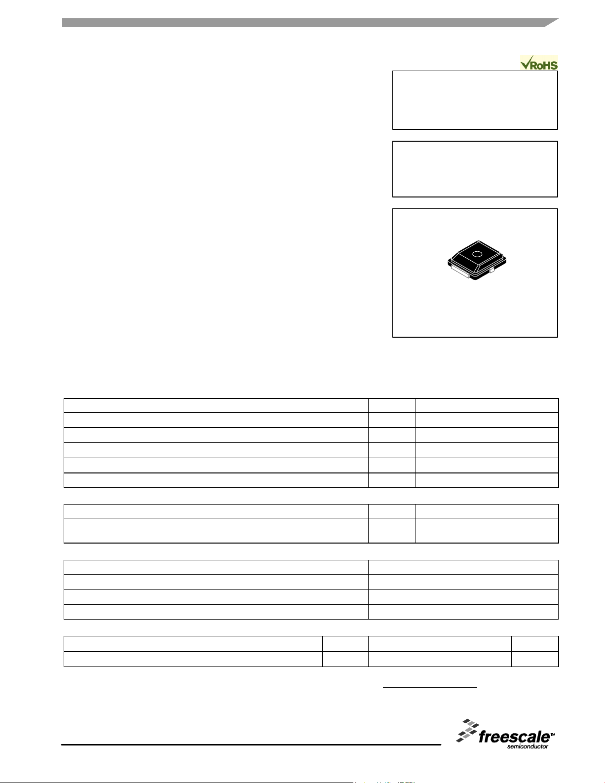
MRFG35010ANT1
3.5 GHz, 9 W, 12 V
POWER FET
GaAs PHEMT
CASE 466-03, STYLE 1
PLD-1.5
PLASTIC
Table 1. Maximum Ratings
Rating Symbol Value Unit
Drain-Source Voltage V
Gate-Source Voltage V
RF Input Power P
Storage Temperature Range T
Channel Temperature
(1)
DSS
GS
stg
T
ch
in
15 Vdc
-5 Vdc
33 dBm
-65 to +150 °C
175 °C
Table 2. Thermal Characteristics
Characteristic Symbol Value
Thermal Resistance, Junction to Case
Case Temperature 77°C, 1 W CW
R
θ
JC
(2)
6.5 °C/W
Table 3. ESD Protection Characteristics
Test Methodology Class
Human Body Model (per JESD22-A114) 2 (Minimum)
Machine Model (per EIA/JESD22-A115) A (Minimum)
Charge Device Model (per JESD22-C101) IV (Minimum)
Table 4. Moisture Sensitivity Level
Test Methodology Rating Package Peak Temperature Unit
Per JESD22-A113, IPC/JEDEC J- STD-020 3 260 °C
1. For reliable operation, the operating channel temperature should not exceed 150°C.
2. Refer to AN1955, Thermal Measurement Methodology of RF Power Amplifiers. Go to http://www.freescale.com/rf
Select Documentation/Application Notes - AN1955.
.
Unit
Freescale Semiconductor, Inc., 2006, 2008- 2009. All rights reserved.
RF Device Data
Freescale Semiconductor
MRFG35010ANT1
1
Page 2
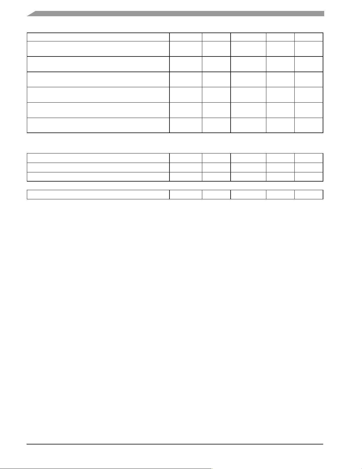
Table 5. Electrical Characteristics
Characteristic
Saturated Drain Current
(V
= 3.5 Vdc, VGS = 0 Vdc)
DS
Off State Leakage Current
= - 0.4 Vdc, VDS = 0 Vdc)
(V
GS
Off State Drain Current
(V
= 12 Vdc, VGS = - 2.2 Vdc)
DS
Off State Current
(V
= 28.5 Vdc, VGS = - 2.5 Vdc)
DS
Gate-Source Cut - off Voltage
(V
= 3.5 Vdc, IDS = 15 mA)
DS
Quiescent Gate Voltage
(V
= 12 Vdc, IDQ = 180 mA)
DS
Functional Tests (In Freescale Test Fixture, 50 ohm system) VDD = 12 Vdc, IDQ = 130 mA, P
(TA = 25°C unless otherwise noted)
Symbol Min Typ Max Unit
I
DSS
I
GSS
I
DSO
I
DSX
V
GS(th)
V
GS(Q)
— 2.9 — Adc
— < 1 100 µAdc
— 0.1 1 mAdc
— 2 15 mAdc
-1.2 -1.0 - 0.7 Vdc
-1.2 - 0.95 - 0.7 Vdc
= 1 W Avg., f = 3550 MHz, Single- Carrier
out
W- CDMA, 3.84 MHz Channel Bandwidth Carrier. ACPR measured in 3.84 MHz Channel Bandwidth @ ±5 MHz Offset.
PAR = 8.5 dB @ 0.01% Probability on CCDF.
Power Gain
Drain Efficiency
G
ps
h
D
9 10 — dB
23 25 — %
Adjacent Channel Power Ratio ACPR — -43 -40 dBc
Typical RF Performance (In Freescale Test Fixture, 50 οhm system) V
Output Power, 1 dB Compression Point, CW
= 12 Vdc, IDQ = 130 mA, f = 3550 MHz
DD
P
1dB
— 9 — W
MRFG35010ANT1
2
RF Device Data
Freescale Semiconductor
Page 3
V
BIAS
C11
C10 C9 C8 C7 C6 C5 C18 C17 C16 C15 C14 C13 C12
C4
C19
V
SUPPLY
Z9
RF
INPUT
Z1 Z2 Z3 Z5 Z6 Z7 Z10 Z11 Z13 Z14 Z17
C1
Z4
C3
C2
Z1 0.045″ x 0.689″ Microstrip
Z2 0.045″ x 0.089″ Microstrip
Z3 0.020″ x 0.360″ Microstrip
Z4 0.045″ x 0.029″ Microstrip
Z5 0.045″ x 0.061″ Microstrip
Z6 0.045″ x 0.055″ Microstrip
Z7 0.300″ x 0.125″ Microstrip
Z8, Z10 0.146″ x 0.070″ Microstrip
Z9 0.025″ x 0.485″ Microstrip
R1
Z8
Z12
Z15 Z16
C22 C21
Z11 0.400″ x 0.215″ Microstrip
Z12 0.025″ x 0.497″ Microstrip
Z13 0.025″ x 0.271″ Microstrip
Z14 0.025″ x 0.363″ Microstrip
Z15 0.025″ x 0.041″ Microstrip
Z16 0.045″ x 0.050″ Microstrip
Z17 0.045″ x 0.467″ Microstrip
PCB Rogers 4350, 0.020″, ε
= 3.5
r
C20
Figure 1. 3.5 GHz Test Circuit Schematic
Table 6. 3.5 GHz Test Circuit Component Designations and Values
Part Description Part Number Manufacturer
C1, C21, C22 0.5 pF Chip Capacitors 08051J0R5BBT AVX
C2 0.2 pF Chip Capacitor 06035J0R2BBT AVX
C3 0.5 pF Chip Capacitor 06035J0R5BBT AVX
C4, C19, C20 6.8 pF Chip Capacitors 08051J6R8BBT AVX
C5, C18 10 pF Chip Capacitors 100A100JP150XT AT C
C6, C17 100 pF Chip Capacitors 100A101JP150XT AT C
C7, C16 100 pF Chip Capacitors 100B101JP500XT AT C
C8, C15 1000 pF Chip Capacitors 100B102JP50XT ATC
C9, C14 0.1 µF Chip Capacitors CDR33BX104AKWS Kemet
C10, C13 39K pF Chip Capacitors 200B393KP50XT ATC
C11, C12 10 µF, 50 V Chip Capacitors GRM55DR61H106KA88B Murata
R1 50 Ω Chip Resistor P51ETR-ND Newark
RF
OUTPUT
RF Device Data
Freescale Semiconductor
MRFG35010ANT1
3
Page 4
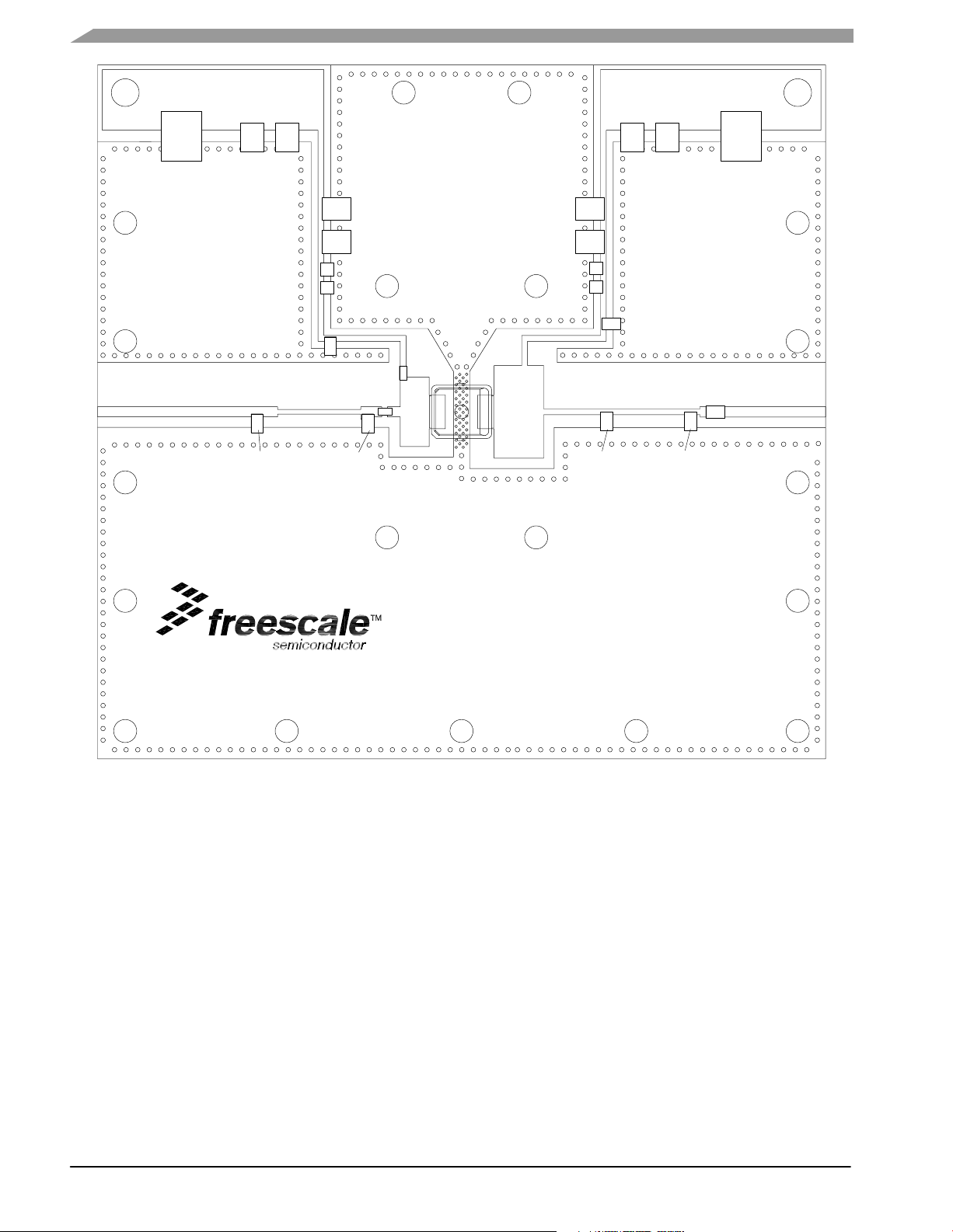
C11
C10 C9
C14 C13
C12
C1
C4
C6
C5
C2
C8
C7
C3
C15
C16
C17
C18
C19
R1
C20
C22 C21
MRFG35010XX, Rev. 5
MRFG35010ANT1
4
Figure 2. 3.5 GHz Test Circuit Component Layout
RF Device Data
Freescale Semiconductor
Page 5

TYPICAL CHARACTERISTICS
12
10
VDS = 12 Vdc, IDQ = 130 mA, f = 3550 MHz
8
Single−Carrier W−CDMA
3.84 MHz Channel Bandwidth
= 0.875 ∠ −131.0_
Γ
S
6
Γ
= 0.849 ∠ −145.8_
L
, TRANSDUCER GAIN (dB)
T
G
4
η
D
2
10
15
20 25 30 35
P
, OUTPUT POWER (dBm)
out
Figure 3. Single- Carrier W -CDMA Power Gain
and Drain Efficiency versus Output Power
−10
VDS = 12 Vdc, IDQ = 130 mA, f = 3550 MHz
Single−Carrier W−CDMA, 3.84 MHz Channel Bandwidth
Γ
−20
−30
= 0.875 ∠ −131.0_, ΓL = 0.849 ∠ −145.8_
S
IRL
50
40
G
T
30
20
, DRAIN EFFICIENCY (%)
D
10
η
0
40
−10
−15
−20
−40
−50
−60
ACPR, ADJACENT CHANNEL POWER RATIO (dBc)
15
ACPR
20
25 30 35
P
, OUTPUT POWER (dBm)
out
Figure 4. Single- Carrier W -CDMA ACPR and
Input Return Loss versus Output Power
NOTE: All data is referenced to package lead interface. ΓS and Γ
All data is generated from load pull, not from the test circuit shown.
−25
INPUT RETURN LOSS (dB)IRL,
−30
−35
40
are the impedances presented to the DUT.
L
RF Device Data
Freescale Semiconductor
MRFG35010ANT1
5
Page 6

TYPICAL CHARACTERISTICS
14
VDS = 12 Vdc, IDQ = 130 mA, f = 3550 MHz
Single−Carrier W−CDMA, 3.84 MHz Channel Bandwidth
12
PAR = 8.5 dB @ 0.01% Probability (CCDF)
10
8
, POWER GAIN (dB)
6
ps
G
4
2
20
G
ps
η
D
24
28 32 36
P
, OUTPUT POWER (dBm)
out
Figure 5. Single- Carrier W -CDMA Power Gain
and Drain Efficiency versus Output Power
−10
VDS = 12 Vdc, IDQ = 140 mA, f = 3550 MHz
Single−Carrier W−CDMA, 3.84 MHz Channel Bandwidth
PAR = 8.5 dB @ 0.01% Probability (CCDF)
−20
−30
IRL
60
50
40
30
20
, DRAIN EFFICIENCY (%)
D
η
10
0
40
−5
−10
−15
−40
−50
−60
ACPR, ADJACENT CHANNEL POWER RATIO (dBc)
20
ACPR
25
P
, OUTPUT POWER (dBm)
out
30 35
Figure 6. Single- Carrier W -CDMA ACPR and
Input Return Loss versus Output Power
NOTE: Data is generated from the test circuit shown.
−20
INPUT RETURN LOSS (dB)IRL,
−25
−30
40
MRFG35010ANT1
6
RF Device Data
Freescale Semiconductor
Page 7

Zo = 25 Ω
Z
load
f = 3550 MHz
V
= 12 Vdc, IDQ = 130 mA, P
DD
f
MHz
Z
source
W
= 1 W Avg.
out
3550 4.0 - j22.6 4.5 - j15.3
Z
= Test circuit impedance as measured from
source
Z
load
Input
Matching
Network
gate to ground.
= Test circuit impedance as measured
from drain to ground.
Device
Under
Test
Z
source
f = 3550 MHz
Z
load
W
Output
Matching
Network
RF Device Data
Freescale Semiconductor
Z
source
Z
load
Figure 7. Series Equivalent Source and Load Impedance
MRFG35010ANT1
7
Page 8

Table 7. Class AB Common Source S- Parameters
f
S
11
GHz
|S11| ∠φ |S21| ∠φ |S12| ∠φ |S22| ∠φ
(VDD = 12 Vdc, IDQ = 130 mA, TA = 25°C, 50 ohm system)
S
21
S
12
S
22
0.5 0.945 - 174.56 4.019 84.19 0.020 3.30 0.780 -179.31
0.55 0.946 -176.04 3.663 82.53 0.020 2.54 0.781 179.94
0.6 0.947 - 177.32 3.366 80.98 0.020 2.19 0.781 179.35
0.65 0.947 -178.45 3.112 79.47 0.020 1.57 0.781 178.72
0.7 0.948 - 179.56 2.895 77.97 0.020 0.87 0.781 178.05
0.75 0.948 179.46 2.706 76.52 0.020 0.62 0.781 177.37
0.8 0.948 178.47 2.540 75.04 0.020 - 0.13 0.780 176.66
0.85 0.948 177.54 2.393 73.57 0.020 -0.49 0.780 175.92
0.9 0.949 176.67 2.262 72.11 0.020 - 0.94 0.781 175.15
0.95 0.950 175.80 2.144 70.67 0.020 -1.83 0.781 174.36
1 0.949 174.99 2.036 69.21 0.020 - 2.42 0.780 173.56
1.05 0.950 174.21 1.944 67.79 0.020 -2.91 0.781 172.68
1.1 0.950 173.45 1.855 66.34 0.020 - 3.44 0.781 171.84
1.15 0.950 172.67 1.775 64.92 0.020 -4.10 0.781 171.00
1.2 0.949 171.97 1.701 63.52 0.020 - 4.38 0.781 170.10
1.25 0.950 171.32 1.634 62.09 0.020 -4.91 0.781 169.21
1.3 0.950 170.63 1.571 60.69 0.020 - 5.31 0.782 168.37
1.35 0.950 169.95 1.513 59.26 0.020 -6.04 0.783 167.37
1.4 0.949 169.34 1.459 57.88 0.020 - 6.58 0.783 166.48
1.45 0.949 168.69 1.409 56.49 0.020 -7.02 0.784 165.70
1.5 0.949 168.05 1.365 55.14 0.020 - 7.32 0.785 164.78
1.55 0.948 168.83 1.317 53.93 0.020 -7.26 0.787 162.67
1.6 0.948 168.16 1.278 52.65 0.020 - 7.55 0.788 162.09
1.65 0.948 167.46 1.238 51.29 0.020 -7.83 0.789 161.44
1.7 0.948 166.80 1.203 50.05 0.020 - 8.50 0.790 160.84
1.75 0.949 166.20 1.168 48.79 0.020 -9.20 0.790 160.36
1.8 0.950 165.51 1.137 47.59 0.020 - 9.26 0.791 159.76
1.85 0.950 164.95 1.108 46.33 0.020 -9.47 0.791 159.37
1.9 0.950 164.28 1.080 45.15 0.020 - 9.71 0.792 158.91
1.95 0.950 163.65 1.053 43.95 0.020 -9.95 0.793 158.40
2 0.951 162.95 1.029 42.80 0.020 -10.45 0.793 158.00
2.05 0.950 162.45 1.004 41.72 0.020 -10.68 0.794 157.80
2.1 0.950 161.82 0.983 40.60 0.020 - 11.15 0.794 157.42
2.15 0.950 161.22 0.962 39.44 0.020 -11.31 0.794 157.19
2.2 0.949 160.64 0.944 38.45 0.020 - 11.94 0.796 157.03
2.25 0.949 160.02 0.926 37.33 0.020 -12.19 0.797 156.78
2.3 0.949 159.39 0.910 36.28 0.020 -12.28 0.796 156.48
2.35 0.951 158.85 0.894 35.26 0.020 -12.28 0.797 156.47
2.4 0.949 158.25 0.880 34.21 0.020 -12.08 0.797 156.16
2.45 0.948 157.61 0.867 33.14 0.020 -12.46 0.796 155.87
2.5 0.949 157.00 0.855 32.09 0.021 -12.24 0.797 155.85
2.55 0.948 156.38 0.843 31.01 0.021 -12.56 0.796 155.53
2.6 0.948 155.73 0.833 29.90 0.021 -12.08 0.796 155.28
2.65 0.946 155.07 0.823 28.86 0.021 -12.64 0.796 155.24
2.7 0.945 154.41 0.813 27.71 0.021 -12.48 0.796 154.81
2.75 0.944 153.70 0.805 26.55 0.022 -13.14 0.794 154.51
MRFG35010ANT1
8
(continued)
RF Device Data
Freescale Semiconductor
Page 9

Table 7. Class AB Common Source S- Parameters (V
f
S
11
GHz
|S11| ∠φ |S21| ∠φ |S12| ∠φ |S22| ∠φ
= 12 Vdc, IDQ = 130 mA, TA = 25°C, 50 ohm system) (continued)
DD
S
21
S
12
S
22
2.8 0.943 153.02 0.796 25.46 0.022 -13.75 0.794 154.30
2.85 0.943 152.31 0.788 24.29 0.022 -14.19 0.794 153.85
2.9 0.942 151.61 0.781 23.11 0.022 -14.81 0.792 153.42
2.95 0.939 150.84 0.775 22.01 0.022 -15.38 0.791 153.00
3 0.942 150.15 0.768 20.75 0.022 -15.83 0.792 152.55
3.05 0.941 149.40 0.761 19.55 0.023 -16.06 0.787 152.10
3.1 0.939 148.59 0.757 18.31 0.023 -16.58 0.789 151.47
3.15 0.939 147.75 0.751 17.03 0.023 -17.33 0.788 150.69
3.2 0.938 146.97 0.747 15.68 0.023 -17.60 0.786 149.89
3.25 0.941 145.84 0.743 14.42 0.023 -18.35 0.789 149.10
3.3 0.937 145.28 0.736 12.96 0.023 -18.68 0.785 148.30
3.35 0.936 144.36 0.733 11.56 0.023 - 19.36 0.780 147.36
3.4 0.935 143.56 0.728 10.18 0.024 -19.65 0.780 146.56
3.45 0.937 142.81 0.724 8.84 0.024 -19.96 0.781 145.50
3.5 0.934 141.86 0.719 7.37 0.024 - 19.70 0.775 144.38
3.55 0.934 140.99 0.716 6.03 0.024 -19.69 0.776 143.47
3.6 0.933 140.12 0.711 4.58 0.025 - 20.44 0.773 142.22
3.65 0.931 139.20 0.708 3.03 0.025 -21.24 0.768 141.01
3.7 0.933 138.37 0.704 1.61 0.025 - 22.19 0.769 140.17
3.75 0.933 137.48 0.700 0.20 0.025 -22.67 0.767 138.91
3.8 0.933 136.55 0.696 -1.33 0.026 - 23.74 0.763 137.79
3.85 0.931 135.57 0.693 - 2.73 0.026 -24.10 0.765 136.96
3.9 0.928 134.64 0.689 - 4.11 0.026 - 24.28 0.767 135.76
3.95 0.925 133.78 0.685 - 5.62 0.026 -24.60 0.765 134.55
4 0.921 133.05 0.682 -7.05 0.026 - 25.13 0.769 133.67
4.05 0.920 132.39 0.678 - 8.42 0.027 -25.07 0.772 132.19
4.1 0.918 131.72 0.675 -9.92 0.027 - 25.69 0.767 130.73
4.15 0.923 130.82 0.673 -11.37 0.027 - 26.05 0.766 129.70
4.2 0.919 129.91 0.669 -12.78 0.028 -26.99 0.768 128.51
4.25 0.922 129.26 0.666 - 14.22 0.028 -27.58 0.762 127.29
4.3 0.924 128.37 0.664 -15.61 0.028 -28.51 0.764 126.49
4.35 0.926 127.34 0.662 - 16.92 0.029 -28.82 0.761 125.41
4.4 0.926 126.32 0.658 -18.36 0.029 -29.48 0.756 124.59
4.45 0.926 125.27 0.658 - 19.76 0.029 -29.54 0.759 123.86
4.5 0.926 124.13 0.657 -21.11 0.030 -30.12 0.758 122.97
4.55 0.925 123.09 0.654 - 22.50 0.030 -30.82 0.753 122.26
4.6 0.924 122.08 0.654 -23.83 0.030 -31.17 0.755 121.74
4.65 0.924 120.81 0.654 - 25.14 0.031 -31.73 0.754 120.88
4.7 0.922 119.61 0.653 - 26.55 0.031 -32.31 0.750 120.35
4.75 0.921 118.44 0.654 - 27.97 0.032 -33.11 0.752 119.79
4.8 0.919 117.22 0.654 - 29.30 0.032 -33.53 0.751 119.03
4.85 0.917 115.94 0.653 - 30.70 0.032 -34.28 0.747 118.53
4.9 0.916 114.60 0.655 - 32.19 0.033 -34.59 0.748 118.03
4.95 0.914 113.24 0.657 - 33.61 0.033 -34.92 0.748 117.16
5 0.912 111.82 0.657 - 35.10 0.034 - 35.27 0.743 116.59
MRFG35010ANT1
RF Device Data
Freescale Semiconductor
9
Page 10

PACKAGE DIMENSIONS
B
ZONE V
ZONE W
A
F
3
0.095
2.41
0.146
3.71
0.115
2.92
21
D
R
L
0.115
2.92
0.020
4
N
0.35 (0.89) X 45 5
K
Q
U
H
4
1
3
G
ZONE X
2
S
VIEW Y- Y
C
__
"
P
YY
NOTES:
1. INTERPRET DIMENSIONS AND TOLERANCES
PER ASME Y14.5M, 1984.
2. CONTROLLING DIMENSION: INCH
3. RESIN BLEED/FLASH ALLOWABLE IN ZONE V, W,
AND X.
STYLE 1:
PIN 1. DRAIN
2. GATE
3. SOURCE
4. SOURCE
CASE 466- 03
10 DRAFT
_
E
SOLDER FOOTPRINT
DIM MIN MAX MIN MAX
A 0.255 0.265 6.48 6.73
B 0.225 0.235 5.72 5.97
C 0.065 0.072 1.65 1.83
D 0.130 0.150 3.30 3.81
E 0.021 0.026 0.53 0.66
F 0.026 0.044 0.66 1.12
G 0.050 0.070 1.27 1.78
H 0.045 0.063 1.14 1.60
J 0.160 0.180 4.06 4.57
K 0.273 0.285 6.93 7.24
L 0.245 0.255 6.22 6.48
N 0.230 0.240 5.84 6.10
P 0.000 0.008 0.00 0.20
Q 0.055 0.063 1.40 1.60
R 0.200 0.210 5.08 5.33
S 0.006 0.012 0.15 0.31
U 0.006 0.012 0.15 0.31
ZONE V 0.000 0.021 0.00 0.53
ZONE W 0.000 0.010 0.00 0.25
ZONE X 0.000 0.010 0.00 0.25
0.51
inches
mm
MILLIMETERSINCHES
ISSUE D
PLD- 1.5
PLASTIC
MRFG35010ANT1
10
RF Device Data
Freescale Semiconductor
Page 11

PRODUCT DOCUMENTATION
Refer to the following documents to aid your design process.
Application Notes
• AN1955: Thermal Measurement Methodology of RF Power Amplifiers
REVISION HISTORY
The following table summarizes revisions to this document.
Revision Date Description
0 May 2006 • Initial Release of Data Sheet
1 Dec. 2008 • Removed ”Operating Case Temperature Range” from Maximum Ratings table so that the maximum
2 June 2009 • Modified data sheet to reflect MSL rating change from 1 to 3 as a result of the standardization of packing
channel temperature rating is the limiting thermal design criteria and not the case temperature range, p. 1
• Added Table 3, ESD Protection Characteristics, p. 1; renumbered subsequent tables
process as described in Product and Process Change Notification number, PCN13516, p. 1
RF Device Data
Freescale Semiconductor
MRFG35010ANT1
11
Page 12

How to Reach Us:
Home Page:
www.freescale.com
Web Support:
http://www.freescale.com/support
USA/Europe or Locations Not Listed:
Freescale Semiconductor, Inc.
Technical Information Center, EL516
2100 East Elliot Road
Tempe, Arizona 85284
1- 800 - 521 - 6274 or +1 -480- 768 - 2130
www.freescale.com/support
Europe, Middle East, and Africa:
Freescale Halbleiter Deutschland GmbH
Technical Information Center
Schatzbogen 7
81829 Muenchen, Germany
+44 1296 380 456 (English)
+46 8 52200080 (English)
+49 89 92103 559 (German)
+33 1 69 35 48 48 (French)
www.freescale.com/support
Japan:
Freescale Semiconductor Japan Ltd.
Headquarters
ARCO Tower 15F
1- 8 - 1, Shimo - Meguro, Meguro- ku,
Tokyo 153 -0064
Japan
0120 191014 or +81 3 5437 9125
support.japan@freescale.com
Asia/Pacific:
Freescale Semiconductor China Ltd.
Exchange Building 23F
No. 118 Jianguo Road
Chaoyang District
Beijing 100022
China
+86 10 5879 8000
support.asia@freescale.com
For Literature Requests Only:
Freescale Semiconductor Literature Distribution Center
1- 800 - 441 - 2447 or +1 -303- 675 - 2140
Fax: +1- 303 - 675 - 2150
LDCForFreescaleSemiconductor@hibbertgroup.com
Information in this document is provided solely to enable system and software
implementers to use Freescale Semiconductor products. There are no express or
implied copyright licenses granted hereunder to design or fabricate any integrated
circuits or integrated circuits based on the information in this document.
Freescale Semiconductor reserves the right to make changes without further notice to
any products herein. Freescale Semiconductor makes no warranty, representation or
guarantee regarding the suitability of its products for any particular purpose, nor does
Freescale Semiconductor assume any liability arising out of the application or use of
any product or circuit, and specifically disclaims any and all liability, including without
limitation consequential or incidental damages. “Typical” parameters that may be
provided in Freescale Semiconductor data sheets and/or specifications can and do
vary in different applications and actual performance may vary over time. All operating
parameters, including “Typicals”, must be validated for each customer application by
customer’s technical experts. Freescale Semiconductor does not convey any license
under its patent rights nor the rights of others. Freescale Semiconductor products are
not designed, intended, or authorized for use as components in systems intended for
surgical implant into the body, or other applications intended to support or sustain life,
or for any other application in which the failure of the Freescale Semiconductor product
could create a situation where personal injury or death may occur. Should Buyer
purchase or use Freescale Semiconductor products for any such unintended or
unauthorized application, Buyer shall indemnify and hold Freescale Semiconductor
and its officers, employees, subsidiaries, affiliates, and distributors harmless against all
claims, costs, damages, and expenses, and reasonable attorney fees arising out of,
directly or indirectly, any claim of personal injury or death associated with such
unintended or unauthorized use, even if such claim alleges that Freescale
Semiconductor was negligent regarding the design or manufacture of the part.
Freescalet and the Freescale logo are trademarks of Freescale Semiconductor, Inc.
All other product or service names are the property of their respective owners.
Freescale Semiconductor, Inc. 2006, 2008- 2009. All rights reserved.
MRFG35010ANT1
Document Number: MRFG35010AN
Rev. 2, 6/2009
12
RF Device Data
Freescale Semiconductor
 Loading...