

C
O
O
Freescale Semiconductor
Technical Data
MRFG35003NT1 replaced by MRFG35003ANT1.
Document Number: MRFG35003N
Rev. 5, 1/2008
Gallium Arsenide PHEMT
MRFG35003NT1
RF Power Field Effect Transistor
Designed for WLL/MMDS/BWA or UMTS driver applications with frequencies
from 1.8 to 3.6 GHz. Device is unmatched and is suitable for use in Class AB
linear base station applications.
• Typical W-CDMA Performance: - 42 dBc ACPR, 3.55 GHz, 12 Volts,
I
= 55 mA, 5 MHz Offset/3.84 MHz BW, 64 DPCH (8.5 dB P/A
DQ
@ 0.01% Probability)
Output Power — 300 mWatt
Power Gain — 11.5 dB
Efficiency — 25%
• 3 Watts P1dB @ 3.55 GHz
N
• Excellent Phase Linearity and Group Delay Characteristics
• High Gain, High Efficiency and High Linearity
• N Suffix Indicates Lead- Free Terminations. RoHS Compliant.
• In Tape and Reel. T1 Suffix = 1000 Units per 12 mm, 7 inch Reel.
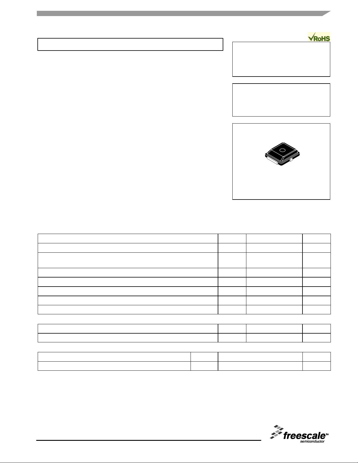
3.5 GHz, 3 W, 12 V
POWER FET
GaAs PHEMT
CASE 466-03, STYLE 1
PLD-1.5
PLASTIC
RMATI
Table 1. Maximum Ratings
Rating Symbol Value Unit
Drain-Source Voltage V
Total Device Dissipation @ TC = 25°C
Derate above 25°C
Gate- Source Voltage V
RF Input Power P
HIVE INF
Storage Temperature Range T
Channel Temperature
Operating Case Temperature Range T
Table 2. Thermal Characteristics
AR
Thermal Resistance, Junction to Case Class AB R
Table 3. Moisture Sensitivity Level
Per JESD 22-A113, IPC/JEDEC J-STD - 020 1 260 °C
1. For reliable operation, the operating channel temperature should not exceed 150°C.
2. Simulated.
(1)
Characteristic Symbol Value Unit
Test Methodology Rating Package Peak Temperature Unit
DSS
P
GS
stg
T
ch
θ
D
in
C
JC
15 Vdc
(2)
8.1
(2)
0.05
-5 Vdc
29 dBm
-65 to +150 °C
175 °C
-20 to +85 °C
(2)
18.5
W
W/°C
ARCHIVE INFORMATION
°C/W
Freescale Semiconductor, Inc., 2006, 2008. All rights reserved.
RF Device Data
Freescale Semiconductor
MRFG35003NT1
1
C
O
O
Table 4. Electrical Characteristics
Characteristic Symbol Min Typ Max Unit
Saturated Drain Current
(V
= 3.5 Vdc, VGS = 0 Vdc)
DS
Off State Leakage Current
(VGS = - 0.4 Vdc, VDS = 0 Vdc)
Off State Drain Current
(VDS = 12 Vdc, VGS = -2.5 Vdc)
Off State Current
(VDS = 28.5 Vdc, VGS = -2.5 Vdc)
Gate- Source Cut - off Voltage
(VDS = 3.5 Vdc, IDS = 6.5 mA)
Quiescent Gate Voltage
(VDS = 12 Vdc, ID = 55 mA)
Power Gain
N
(VDD = 12 Vdc, IDQ = 55 mA, f = 3.55 GHz)
Output Power, 1 dB Compression Point
(VDD = 12 Vdc, IDQ = 55 mA, f = 3.55 GHz)
Drain Efficiency
(VDD = 12 Vdc, IDQ = 55 mA, P
f = 3.55 GHz)
Adjacent Channel Power Ratio
(VDD = 12 Vdc, P
f = 3.55 GHz, W- CDMA, 8.5 P/A @ 0.01% Probability,
RMATI
64 CH, 3.84 MCPS)
= 0.30 W Avg., IDQ = 55 mA,
out
(TC = 25°C unless otherwise noted)
= 0.30 W Avg.,
out
I
DSS
I
GSS
I
DSO
I
DSX
V
GS(th)
V
GS(Q)
G
ps
P
1dB
h
D
ACPR — -42 -40 dBc
— 1.3 — Adc
— < 1.0 100 µAdc
— — 450 µAdc
— < 1.0 7 mAdc
-1.2 -0.9 - 0.7 Vdc
-1.2 -0.9 - 0.7 Vdc
10 11.5 — dB
— 3 — W
23 25 — %
HIVE INF
AR
MRFG35003NT1
2
ARCHIVE INFORMATION
RF Device Data
Freescale Semiconductor
C
O
O
V
GS
N
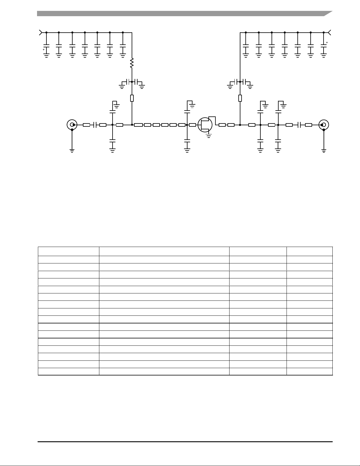
C10
C9 C8 C7 C6 C5 C4
RF
INPUT
Z1 Z2 Z3 Z4 Z10 Z11 Z12 Z13 Z14 Z16 Z17 Z18
C1 C20
C13 C14 C15 C16 C17 C18 C19
R1
C2 C3 C11 C12
Z5 Z15
C21 C22 C24
Z9Z8Z6 Z7
C23
C26
C25C27C28
V
RF
OUTPUT
DD
Z1, Z18 0.125″ x 0.044″ Microstrip
Z2 0.409″ x 0.044″ Microstrip
Z3 0.326″ x 0.288″ Microstrip
Z4 0.333″ x 0.572″ Microstrip
Z5, Z15 0.527″ x 0.015″ Microstrip
RMATI
Table 5. 3.5 GHz Test Circuit Component Designations and Values
Part Description Part Number Manufacturer
C1, C20 7.5 pF Chip Capacitors 100A7R5JP150X AT C
C2, C3, C11, C12 3.9 pF Chip Capacitors (0805) 08051J3R9BBT AV X
C4, C13 10 pF Chip Capacitors 100A100JP500X ATC
C5, C14 100 pF Chip Capacitors 100A101JP500X ATC
HIVE INF
C6, C15 100 pF Chip Capacitors 100B101JP500X ATC
C7, C16 1000 pF Chip Capacitors 100B102JP500X ATC
C8, C17 3.9 µF Chip Capacitors ATC
C9, C18 0.1 µF Chip Capacitors ATC
C10, C19 22 µF, 35 V Tantalum Surface Mount Capacitors ATC
AR
C21 0.7 pF Chip Capacitor (0805) 08051J0R7BBT AVX
C22, C27 0.2 pF Chip Capacitors (0805) 08051J0R2BBT AVX
C23, C28 0.8 pF Chip Capacitors (0805) 08051J0R8BBT AVX
C24 1.0 pF Chip Capacitor 08051J1R0BBT AVX
C25 1.2 pF Chip Capacitor 08051J1R2BBT AVX
C26 0.5 pF Chip Capacitor 08051J0R5BBT AVX
R1
Z6, Z8, Z10 0.050″ x 0.025″ Microstrip
Z7, Z9 0.097″ x 0.025″ Microstrip
Figure 1. 3.5 GHz Test Circuit Schematic
100 W Chip Resistor
Z11 0.082″ x 0.372″ Microstrip
Z12 0.169″ x 0.471″ Microstrip
Z13 0.196″ x 0.093″ Microstrip
Z14 0.313″ x 0.338″ Microstrip
Z16 0.200″ x 0.065″ Microstrip
Z17 0.472″ x 0.044″ Microstrip
PCB Rogers 4350, 0.020″, εr = 3.5
ARCHIVE INFORMATION
Newark
RF Device Data
Freescale Semiconductor
MRFG35003NT1
3

C
O
O
C10
C9
C8 C7
C2
R1
C6
C5
C4
C3
C15
C14
C13
C11
C16
C12
C17
C18
C19
N
C1
RMATI
HIVE INF
Freescale has begun the transition of marking Printed Circuit Boards (PCBs) with the Freescale Semiconductor
signature/logo. PCBs may have either Motorola or Freescale markings during the transition period. These changes will have
no impact on form, fit or function of the current product.
C21
C28
C22
C27
C23
C24
C25
C26
MRFG35003M
Rev 1
C20
AR
MRFG35003NT1
4
Figure 2. 3.5 GHz Test Circuit Component Layout
ARCHIVE INFORMATION
RF Device Data
Freescale Semiconductor

C
O
O
TYPICAL CHARACTERISTICS
N
RMATI
0
−10 −10
−20 −20
VDS = 12 Vdc, IDQ = 50 mA
f = 3.55 GHz, 8.5 P/A 3GPP W−CDMA
−30 −30
ΓS = 0.813é−106.27_, ΓL = 0.734é−142.65_
−40 −40
INPUT RETURN LOSS (dB)IRL,
−50 −50
−60
0.01
P
, OUTPUT POWER (WATTS)
out
Figure 3. W- CDMA ACPR and Input Return
Loss versus Output Power
18
VDS = 12 Vdc, IDQ = 50 mA
f = 3.55 GHz, 8.5 P/A 3GPP W−CDMA
16 40
ΓS = 0.813é−106.27_, ΓL = 0.734é−142.65_
14 35
12 30
0.1
IRL
ACPR
PAE
G
T
0
ACPR (dBc)
−60
1
45
HIVE INF
NOTE: All data is referenced to package lead interface. ΓS and Γ
All data is generated from load pull, not from the test circuit shown.
AR
10 25
820
, TRANSDUCER GAIN (dB)
T
615
G
410
2
0.01
P
, OUTPUT POWER (WATTS)
out
Figure 4. Transducer Gain and Power Added
Efficiency versus Output Power
0.1
are the impedances presented to the DUT.
L
PAE, POWER ADDED EFFICIENCY (%)
5
1
ARCHIVE INFORMATION
RF Device Data
Freescale Semiconductor
MRFG35003NT1
5

C
O
O
Table 6. Class AB Common Source S- Parameters at V
f
S
11
GHz
0.50 0.879 -160.58 8.644 88.22 0.038 6.94 0.520 -161.47
0.55 0.879 -163.33 7.924 85.88 0.039 5.42 0.520 -163.29
0.60 0.877 -166.03 7.317 83.57 0.039 3.80 0.520 -165.21
0.65 0.876 -168.54 6.811 81.29 0.039 2.37 0.520 -167.01
0.70 0.877 -170.64 6.380 79.13 0.039 0.94 0.521 -168.58
0.75 0.875 -172.68 5.988 77.06 0.039 -0.41 0.520 - 170.13
0.80 0.877 -174.56 5.653 75.00 0.040 -1.67 0.520 - 171.60
0.85 0.876 -176.25 5.310 72.83 0.040 -2.81 0.520 - 172.89
0.90 0.874 -177.90 5.058 71.00 0.040 -4.01 0.519 - 174.37
0.95 0.875 -179.54 4.825 69.08 0.040 -5.15 0.520 - 175.84
1.00 0.876 179.00 4.608 67.27 0.040 -6.31 0.520 -177.05
1.05 0.875 177.53 4.411 65.38 0.040 -7.28 0.519 -178.37
N
1.10 0.874 176.04 4.224 63.51 0.040 -8.43 0.520 -179.67
1.15 0.875 174.55 4.056 61.69 0.040 -9.47 0.521 179.15
1.20 0.874 173.13 3.894 59.88 0.040 - 10.47 0.520 177.91
1.25 0.873 171.63 3.743 58.01 0.040 -11.78 0.521 176.52
1.30 0.876 170.20 3.609 56.26 0.040 - 12.79 0.522 175.56
1.35 0.871 168.97 3.479 54.57 0.040 - 13.72 0.520 174.80
1.40 0.878 167.17 3.355 52.76 0.040 - 14.65 0.526 173.34
1.45 0.876 165.98 3.237 51.14 0.040 - 15.48 0.526 172.88
RMATI
1.50 0.874 162.45 3.118 49.25 0.040 - 16.80 0.528 174.64
1.55 0.874 161.17 3.024 47.67 0.040 - 17.76 0.529 173.65
1.60 0.874 160.09 2.929 46.14 0.040 - 18.51 0.530 172.88
1.65 0.876 159.00 2.848 44.54 0.040 - 19.27 0.530 172.31
1.70 0.878 157.85 2.767 42.99 0.039 - 20.03 0.531 171.29
1.75 0.878 156.84 2.690 41.32 0.039 - 20.89 0.533 170.58
1.80 0.878 155.94 2.625 39.82 0.039 - 21.53 0.533 170.03
1.85 0.880 154.93 2.557 38.21 0.039 - 22.22 0.533 168.95
1.90 0.879 154.05 2.492 36.74 0.039 - 23.01 0.536 168.19
1.95 0.879 153.24 2.434 35.28 0.039 - 23.74 0.535 167.63
HIVE INF
2.00 0.881 152.32 2.379 33.68 0.039 - 24.55 0.535 166.68
2.05 0.881 151.56 2.325 32.27 0.040 - 25.32 0.538 165.91
2.10 0.880 150.85 2.279 30.90 0.040 - 25.97 0.539 165.46
2.15 0.881 149.96 2.236 29.41 0.040 - 26.76 0.537 164.56
2.20 0.881 149.27 2.191 27.93 0.040 - 27.75 0.539 163.66
AR
2.25 0.880 148.61 2.151 26.53 0.040 - 28.56 0.541 163.24
2.30 0.880 147.74 2.121 24.99 0.040 - 29.32 0.539 162.46
2.35 0.881 146.91 2.084 23.54 0.040 - 29.95 0.539 161.41
2.40 0.879 146.12 2.051 22.12 0.040 - 30.72 0.540 160.97
2.45 0.877 145.07 2.023 20.46 0.040 - 31.44 0.539 160.26
2.50 0.876 144.07 1.992 18.93 0.040 - 32.36 0.539 159.16
2.55 0.876 143.15 1.971 17.38 0.040 - 32.95 0.541 158.56
2.60 0.873 142.10 1.948 15.95 0.041 - 33.58 0.538 157.90
2.65 0.872 140.88 1.924 14.31 0.041 - 34.41 0.538 156.83
2.70 0.872 139.83 1.901 12.69 0.041 - 35.22 0.538 156.16
2.75 0.867 138.60 1.882 11.19 0.042 - 36.04 0.537 155.70
2.80 0.868 137.26 1.864 9.40 0.042 - 37.16 0.535 154.59
|S11| ∠φ |S21| ∠φ |S12| ∠φ |S22| ∠φ
= 12 Vdc, IDQ = 50 mA
DS
S
21
S
12
S
22
ARCHIVE INFORMATION
MRFG35003NT1
6
RF Device Data
Freescale Semiconductor

C
O
O
f
Table 6. Class AB Common Source S- Parameters at VDS = 12 Vdc, IDQ = 50 mA (continued)
S
11
GHz
2.85 0.868 136.03 1.845 7.80 0.043 - 38.56 0.537 153.86
2.90 0.866 134.67 1.828 6.20 0.043 - 39.94 0.536 153.32
2.95 0.866 133.02 1.812 4.39 0.043 - 41.41 0.534 152.08
3.00 0.868 131.47 1.795 2.53 0.043 - 42.49 0.536 151.08
3.05 0.865 129.99 1.780 0.80 0.043 - 43.57 0.535 150.49
3.10 0.864 128.11 1.766 -1.00 0.043 -44.68 0.532 149.20
3.15 0.865 126.39 1.745 -2.87 0.043 -45.67 0.533 148.09
3.20 0.864 124.86 1.728 -4.58 0.043 -46.62 0.533 147.42
3.25 0.861 122.97 1.714 -6.48 0.043 -47.78 0.531 146.29
3.30 0.863 121.30 1.697 -8.33 0.043 -49.02 0.532 145.13
3.35 0.862 119.77 1.681 -9.97 0.043 -49.91 0.532 144.52
3.40 0.860 117.84 1.665 - 11.83 0.043 - 50.93 0.529 143.46
N
3.45 0.862 116.26 1.648 - 13.70 0.043 - 51.73 0.529 142.35
3.50 0.861 114.65 1.630 - 15.43 0.043 - 52.55 0.530 141.50
3.55 0.860 112.77 1.620 - 17.24 0.044 - 53.64 0.527 140.51
3.60 0.862 111.19 1.602 -18.99 0.044 - 54.74 0.525 139.19
3.65 0.861 109.76 1.584 - 20.65 0.044 - 55.56 0.525 138.23
3.70 0.860 108.08 1.572 - 22.49 0.044 - 56.84 0.524 137.30
3.75 0.861 106.70 1.557 - 24.18 0.044 -58.11 0.523 136.00
3.80 0.862 105.31 1.544 - 25.86 0.044 - 59.31 0.524 134.95
RMATI
3.85 0.862 103.85 1.533 - 27.47 0.044 - 60.49 0.523 134.13
3.90 0.861 102.50 1.519 - 29.14 0.044 - 61.50 0.521 132.71
3.95 0.862 101.16 1.508 - 30.97 0.044 - 62.41 0.522 131.61
4.00 0.861 99.84 1.499 -32.49 0.044 - 63.14 0.520 130.97
4.05 0.861 98.44 1.494 -34.26 0.044 - 64.07 0.518 129.57
4.10 0.861 97.12 1.482 -35.96 0.044 - 64.91 0.518 128.23
4.15 0.859 96.07 1.474 -37.51 0.045 - 65.77 0.515 127.49
4.20 0.858 94.61 1.471 -39.42 0.045 - 67.06 0.512 125.93
4.25 0.859 93.26 1.463 -41.19 0.045 - 68.21 0.512 124.32
4.30 0.859 92.06 1.458 -42.86 0.045 - 69.40 0.511 123.47
HIVE INF
4.35 0.857 90.72 1.457 -44.58 0.046 - 70.54 0.507 122.03
4.40 0.857 89.22 1.450 -46.51 0.046 - 71.95 0.508 120.25
4.45 0.855 87.99 1.446 -48.27 0.046 - 73.34 0.508 119.27
4.50 0.855 86.49 1.453 -50.09 0.047 - 74.58 0.504 117.72
AR
4.55 0.855 84.61 1.448 -52.14 0.046 - 75.92 0.503 115.65
4.60 0.854 83.10 1.449 -53.98 0.047 - 76.82 0.501 114.46
4.65 0.853 81.10 1.454 -56.16 0.047 - 78.14 0.495 112.83
4.70 0.851 78.94 1.450 -58.44 0.048 - 79.84 0.492 110.59
4.75 0.851 77.09 1.450 -60.56 0.048 - 81.55 0.491 109.01
4.80 0.848 74.85 1.450 -62.75 0.048 - 83.28 0.486 107.24
4.85 0.849 72.60 1.448 -65.03 0.048 - 84.88 0.483 105.01
4.90 0.845 70.48 1.443 -67.33 0.048 - 86.30 0.482 103.27
4.95 0.841 68.09 1.443 -69.60 0.048 - 87.72 0.477 101.51
5.00 0.841 65.50 1.442 -72.12 0.048 - 89.22 0.474 99.28
|S11| ∠φ |S21| ∠φ |S12| ∠φ |S22| ∠φ
S
21
S
12
S
22
ARCHIVE INFORMATION
RF Device Data
Freescale Semiconductor
MRFG35003NT1
7

C
O
O
PACKAGE DIMENSIONS
N
RMATI
B
ZONE V
ZONE W
A
F
3
21
D
4
N
K
Q
H
4
1
3
G
ZONE X
VIEW Y- Y
R
0.35 (0.89) X 45 5
U
2
S
L
C
__
"
P
YY
NOTES:
1. INTERPRET DIMENSIONS AND TOLERANCES
PER ASME Y14.5M, 1984.
2. CONTROLLING DIMENSION: INCH
3. RESIN BLEED/FLASH ALLOWABLE IN ZONE V, W,
AND X.
STYLE 1:
PIN 1. DRAIN
2. GATE
3. SOURCE
4. SOURCE
CASE 466- 03
ISSUE D
PLD- 1.5
0.095
2.41
10 DRAFT
_
E
0.115
2.92
ZONE V 0.000 0.021 0.00 0.53
ZONE W 0.000 0.010 0.00 0.25
ZONE X 0.000 0.010 0.00 0.25
0.146
3.71
0.115
2.92
0.020
0.51
SOLDER FOOTPRINT
DIM MIN MAX MIN MAX
A 0.255 0.265 6.48 6.73
B 0.225 0.235 5.72 5.97
C 0.065 0.072 1.65 1.83
D 0.130 0.150 3.30 3.81
E 0.021 0.026 0.53 0.66
F 0.026 0.044 0.66 1.12
G 0.050 0.070 1.27 1.78
H 0.045 0.063 1.14 1.60
J 0.160 0.180 4.06 4.57
K 0.273 0.285 6.93 7.24
L 0.245 0.255 6.22 6.48
N 0.230 0.240 5.84 6.10
P 0.000 0.008 0.00 0.20
Q 0.055 0.063 1.40 1.60
R 0.200 0.210 5.08 5.33
S 0.006 0.012 0.15 0.31
U 0.006 0.012 0.15 0.31
MILLIMETERSINCHES
inches
mm
PLASTIC
HIVE INF
AR
MRFG35003NT1
8
ARCHIVE INFORMATION
RF Device Data
Freescale Semiconductor

C
O
O
REVISION HISTORY
The following table summarizes revisions to this document.
Revision Date Description
5 Jan. 2008 • Listed replacement part, p. 1
• Added Revision History, p. 9
N
RMATI
HIVE INF
AR
ARCHIVE INFORMATION
RF Device Data
Freescale Semiconductor
MRFG35003NT1
9

C
O
O
How to Reach Us:
Home Page:
www.freescale.com
Web Support:
http://www.freescale.com/support
N
USA/Europe or Locations Not Listed:
Freescale Semiconductor, Inc.
Technical Information Center, EL516
2100 East Elliot Road
Tempe, Arizona 85284
+1-800 - 521 - 6274 or +1 - 480 -768-2130
www.freescale.com/support
Europe, Middle East, and Africa:
Freescale Halbleiter Deutschland GmbH
RMATI
Technical Information Center
Schatzbogen 7
81829 Muenchen, Germany
+44 1296 380 456 (English)
+46 8 52200080 (English)
+49 89 92103 559 (German)
+33 1 69 35 48 48 (French)
www.freescale.com/support
Japan:
Freescale Semiconductor Japan Ltd.
Headquarters
ARCO Tower 15F
1-8 - 1, Shimo - Meguro, Meguro - ku,
Tokyo 153-0064
Japan
0120 191014 or +81 3 5437 9125
HIVE INF
support.japan@freescale.com
Asia/Pacific:
Freescale Semiconductor Hong Kong Ltd.
Technical Information Center
2 Dai King Street
Tai Po Industrial Estate
AR
Tai Po, N.T., Hong Kong
+800 2666 8080
support.asia@freescale.com
For Literature Requests Only:
Freescale Semiconductor Literature Distribution Center
P.O. Box 5405
Denver, Colorado 80217
1-800 - 441 - 2447 or 303 - 675 -2140
Fax: 303-675 - 2150
LDCForFreescaleSemiconductor@hibbertgroup.com
Information in this document is provided solely to enable system and software
implementers to use Freescale Semiconductor products. There are no express or
implied copyright licenses granted hereunder to design or fabricate any integrated
circuits or integrated circuits based on the information in this document.
Freescale Semiconductor reserves the right to make changes without further notice to
any products herein. Freescale Semiconductor makes no warranty, representation or
guarantee regarding the suitability of its products for any particular purpose, nor does
Freescale Semiconductor assume any liability arising out of the application or use of
any product or circuit, and specifically disclaims any and all liability, including without
limitation consequential or incidental damages. “Typical” parameters that may be
provided in Freescale Semiconductor data sheets and/or specifications can and do
vary in different applications and actual performance may vary over time. All operating
parameters, including “Typicals”, must be validated for each customer application by
customer’s technical experts. Freescale Semiconductor does not convey any license
under its patent rights nor the rights of others. Freescale Semiconductor products are
not designed, intended, or authorized for use as components in systems intended for
surgical implant into the body, or other applications intended to support or sustain life,
or for any other application in which the failure of the Freescale Semiconductor product
could create a situation where personal injury or death may occur. Should Buyer
purchase or use Freescale Semiconductor products for any such unintended or
unauthorized application, Buyer shall indemnify and hold Freescale Semiconductor
and its officers, employees, subsidiaries, affiliates, and distributors harmless against all
claims, costs, damages, and expenses, and reasonable attorney fees arising out of,
directly or indirectly, any claim of personal injury or death associated with such
unintended or unauthorized use, even if such claim alleges that Freescale
Semiconductor was negligent regarding the design or manufacture of the part.
Freescalet and the Freescale logo are trademarks of Freescale Semiconductor, Inc.
All other product or service names are the property of their respective owners.
Freescale Semiconductor, Inc. 2006, 2008. All rights reserved.
ARCHIVE INFORMATION
MRFG35003NT1
Document Number: MRFG35003N
Rev. 5, 1/2008
10
RoHS-compliant and/or Pb -free versions of Freescale products have the functionality and electrical
characteristics of their non-RoHS- compliant and/or non-Pb -free counterparts. For further
information, see http://www.freescale.com or contact your Freescale sales representative.
For information on Freescale’s Environmental Products program, go to http://www.freescale.com/epp.
RF Device Data
Freescale Semiconductor
 Loading...