

Page 1
C
O
O
Freescale Semiconductor
Technical Data
MRFG35002N6T1 replaced by MRFG35002N6AT1.
Gallium Arsenide PHEMT
RF Power Field Effect Transistor
Designed for WLL/MMDS/BWA or UMTS driver applications. Characterized
from 500 to 5000 MHz. Device is unmatched and is suitable for use in Class AB
Customer Premise Equipment (CPE) applications.
• Typical Single-Carrier W - CDMA Performance: V
65 mA, P
3.84 MHz, PAR = 8.5 dB @ 0.01% Probability on CCDF.
Power Gain — 10 dB
Drain Efficiency — 27%
ACPR @ 5 MHz Offset — -41 dBc in 3.84 MHz Channel Bandwidth
• 1.5 Watts P1dB @ 3550 MHz, CW
N
• Excellent Phase Linearity and Group Delay Characteristics
• High Gain, High Efficiency and High Linearity
• RoHS Compliant.
• In Tape and Reel. T1 Suffix = 1000 Units per 12 mm, 7 inch Reel.
= 158.5 mWatts Avg., 3550 MHz, Channel Bandwidth =
out
= 6 Volts, IDQ =
DD
Document Number: MRFG35002N6
Rev. 2, 1/2008
MRFG35002N6T1
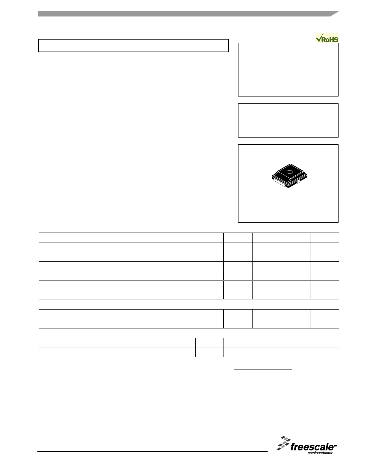
3.5 GHz, 1.5 W, 6 V
POWER FET
GaAs PHEMT
CASE 466-03, STYLE 1
RMATI
Table 1. Maximum Ratings
Rating Symbol Value Unit
Drain-Source Voltage V
Gate-Source Voltage V
RF Input Power P
Storage Temperature Range T
Channel Temperature
HIVE INF
Operating Case Temperature Range T
Table 2. Thermal Characteristics
Thermal Resistance, Junction to Case R
AR
Table 3. Moisture Sensitivity Level
Per JESD 22-A113, IPC/JEDEC J - STD -020 1 260 °C
1. For reliable operation, the operating channel temperature should not exceed 150°C.
2. Refer to AN1955, Thermal Measurement Methodology of RF Power Amplifiers. Go to http://www.freescale.com/rf.
Select Documentation/Application Notes - AN1955.
(1)
Characteristic Symbol Value
Test Methodology Rating Package Peak Temperature Unit
DSS
GS
stg
T
ch
θ
in
C
JC
PLD-1.5
PLASTIC
8 Vdc
-5 Vdc
22 dBm
-65 to +150 °C
175 °C
-20 to +85 °C
(2)
15.2 °C/W
Unit
ARCHIVE INFORMATION
Freescale Semiconductor, Inc., 2006, 2008. All rights reserved.
RF Device Data
Freescale Semiconductor
MRFG35002N6T1
1
Page 2

C
O
O
Table 4. Electrical Characteristics
Characteristic Symbol Min Typ Max Unit
Saturated Drain Current
(V
= 3.5 Vdc, VGS = 0 Vdc)
DS
Off State Leakage Current
(VGS = - 0.4 Vdc, VDS = 0 Vdc)
Off State Drain Current
(VDS = 6 Vdc, VGS = -2.5 Vdc)
Off State Current
(VDS = 28.5 Vdc, VGS = -2.5 Vdc)
Gate-Source Cut-off Voltage
(VDS = 3.5 Vdc, IDS = 8.7 mA)
Quiescent Gate Voltage
(VDS = 6 Vdc, ID = 65 mA)
Functional Tests (In Freescale Test Fixture, 50 ohm system) VDD = 6 Vdc, IDQ = 65 mA, P
N
Single-Carrier W-CDMA, 3.84 MHz Channel Bandwidth Carrier. ACPR measured in 3.84 MHz Channel Bandwidth @ ±5 MHz Offset.
PAR = 8.5 dB @ 0.01% Probability on CCDF.
Power Gain G
Drain Efficiency
Adjacent Channel Power Ratio ACPR — -41 -38 dBc
Typical RF Performance (In Freescale Test Fixture, 50 οhm system) V
Output Power, 1 dB Compression Point, CW P
(TC = 25°C unless otherwise noted)
I
DSS
I
GSS
I
DSO
I
DSX
V
GS(th)
V
GS(Q)
h
= 6 Vdc, IDQ = 65 mA, f = 3550 MHz
DD
1dB
— 1.7 — Adc
— < 1.0 100 µAdc
— — 600 µAdc
— < 1.0 9 mAdc
-1.2 - 0.9 - 0.7 Vdc
-1.1 - 0.8 - 0.6 Vdc
= 158.5 mW Avg., f = 3550 MHz,
out
ps
D
8.5 10 — dB
23 27 — %
— 1.5 — W
RMATI
HIVE INF
AR
MRFG35002N6T1
2
ARCHIVE INFORMATION
RF Device Data
Freescale Semiconductor
Page 3
C
O
O
V
BIAS
V
SUPPLY
N
RMATI
RF
INPUT
C8
C13
C12 C11 C10 C9 C17 C16 C15 C14
Z1 Z2 Z3 Z5 Z7 Z9 Z10 Z12 Z14
C1
Z1, Z14 0.044″ x 0.125″ Microstrip
Z2 0.044″ x 0.500″ Microstrip
Z3 0.044″ x 0.052″ Microstrip
Z4 0.468″ x 0.010″ Microstrip
Z5 0.468″ x 0.356″ Microstrip
Z6, Z11 0.015″ x 0.549″ Microstrip
Z7 0.031″ x 0.259″ Microstrip
Z4
C3
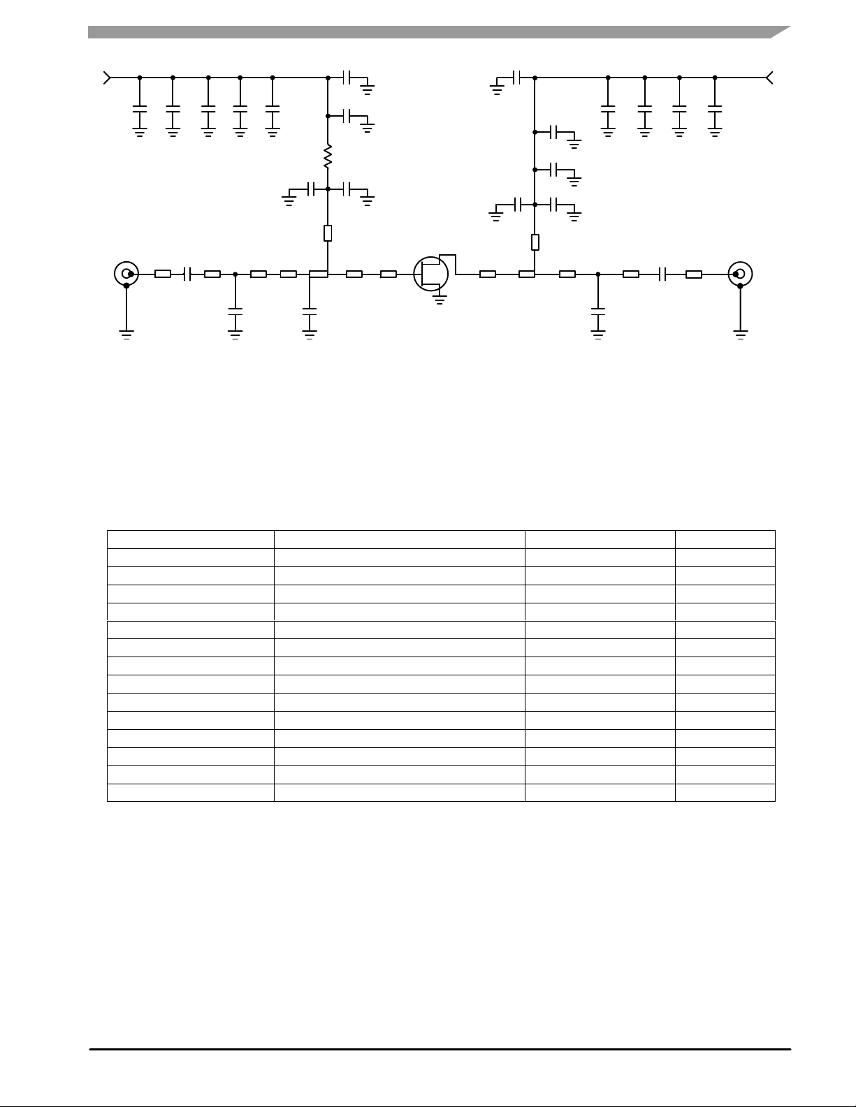
Figure 1. MRFG35002N6 Test Circuit Schematic
C6
C7
R1
C5
Z6
Z8
C4
C18
C19
C20
C21C22
Z11
Z13
C24
C23
Z8 0.420″ x 0.150″ Microstrip
Z9 0.150″ x 0.068″ Microstrip
Z10 0.290″ x 0.183″ Microstrip
Z12 0.044″ x 0.115″ Microstrip
Z13 0.044″ x 0.894″ Microstrip
PCB Rogers 4350, 0.020″, εr = 3.5
RF
OUTPUT
Table 5. MRFG35002N6 Test Circuit Component Designations and Values
Part Description Part Number Manufacturer
C1, C24 13 pF Chip Capacitors 100A130JP150X ATC
C2 Not Used
C3 1.2 pF Chip Capacitor 08051J1R2BBT AVX
C4 0.7 pF Chip Capacitor 08051J0R7BBT AVX
C5, C6, C21, C22 5.6 pF Chip Capacitors 08051J6R8BBT AVX
C7, C20 10 pF Chip Capacitors 100A100JP150X ATC
C8, C19 100 pF Chip Capacitors 100A101JP150X ATC
C9, C18 100 pF Chip Capacitors 100B101JP500X ATC
HIVE INF
C10, C17 1000 pF Chip Capacitors 100B102JP50X ATC
C11, C16 0.1 µF Chip Capacitors CDR33BX104AKWS Kemet
C12, C15 39K pF Chip Capacitors 200B393KP50X ATC
C13, C14 10 µF Chip Capacitors GRM55DR61H106KA88B Kemet
AR
C23 0.2 pF Chip Capacitor 08051J0R2BBT AVX
R1 100 Ω, 1/4 W Chip Resistor
ARCHIVE INFORMATION
RF Device Data
Freescale Semiconductor
MRFG35002N6T1
3
Page 4
C
O
O
C13
C12 C11C12 C10 C9
C5
C8
C7
R1
C6
C18
C14
C15C16C17
C19
C20
C21C22
N
C1
RMATI
HIVE INF
C2
C3
C4
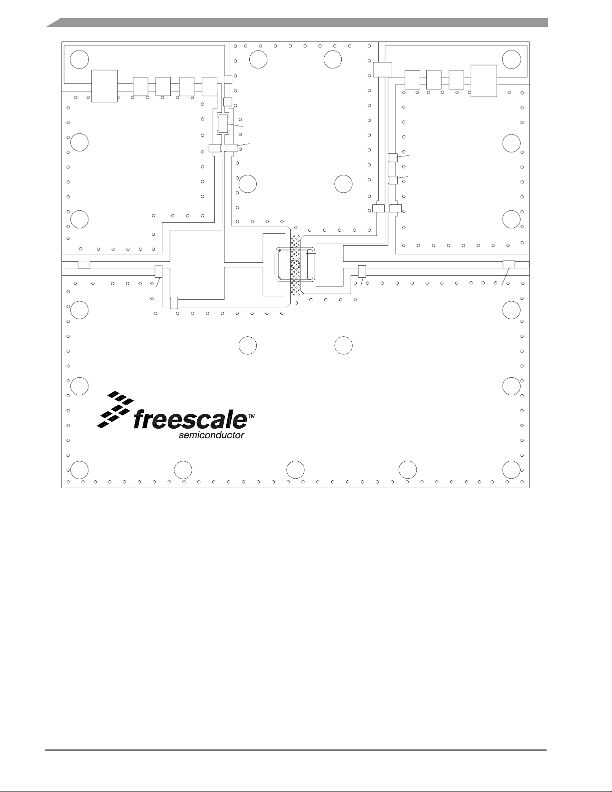
Figure 2. MRFG35002N6 Test Circuit Component Layout
C23
MRFG35002M6, Rev. 2
3.5 GHz - 3.6 GHz
C24
AR
MRFG35002N6T1
4
ARCHIVE INFORMATION
RF Device Data
Freescale Semiconductor
Page 5

C
O
O
TYPICAL CHARACTERISTICS
N
RMATI
14
VDS = 6 Vdc, IDQ = 75 mA, f = 3550 MHz
Single−Carrier W−CDMA, 3.84 MHz Channel Bandwidth
12
ΓS = 0.813é−115.4_, ΓL = 0.748é−147.8_
G
10
8
, TRANSDUCER GAIN (dB)
T
G
6
4
0
−20
VDS = 6 Vdc, IDQ = 75 mA, f = 3550 MHz
Single−Carrier W−CDMA, 3.84 MHz Channel Bandwidth
ΓS = 0.813é−115.4_, ΓL = 0.748é−147.8_
−30
−40
T
η
D
5
Figure 3. Transducer Gain and Drain
Efficiency versus Output Power
10 15 20 25
P
, OUTPUT POWER (dBm)
out
IRL
50
40
30
20
, DRAIN EFFICIENCY (%)
D
10
η
0
30
0
−5
−10
HIVE INF
NOTE: All data is referenced to package lead interface. ΓS and Γ
All data is generated from load pull, not from the test circuit shown.
AR
−50 −15
ACPR
−60
ACPR, ADJACENT CHANNEL POWER RATIO (dBc)
0
Figure 4. Single-Carrier W- CDMA ACPR and
6
Input Return Loss versus Output Power
12 18 24
P
, OUTPUT POWER (dBm)
out
are the impedances presented to the DUT.
L
INPUT RETURN LOSS (dB)IRL,
−20
30
ARCHIVE INFORMATION
RF Device Data
Freescale Semiconductor
MRFG35002N6T1
5
Page 6

C
O
O
TYPICAL CHARACTERISTICS
N
RMATI
14
VDS = 6 Vdc, IDQ = 65 mA, f = 3550 MHz
Single−Carrier W−CDMA, 3.84 MHz Channel Bandwidth
12
PAR = 8.5 dB @ 0.01% Probability (CCDF)
10
8
, POWER GAIN (dB)
ps
G
610
4
0
Figure 5. Single-Carrier W- CDMA Power Gain
and Drain Efficiency versus Output Power
−20
VDS = 6 Vdc, IDQ = 65 mA, f = 3550 MHz
Single−Carrier W−CDMA, 3.84 MHz Channel Bandwidth
PAR = 8.5 dB @ 0.01% Probability (CCDF)
−30
−40
G
ps
η
D
6
12 18 24
P
, OUTPUT POWER (dBm)
out
IRL
50
40
30
20
, DRAIN EFFICIENCY (%)
D
η
0
30
−5
−10
−15
HIVE INF
AR
−50
ACPR
−60
ACPR, ADJACENT CHANNEL POWER RATIO (dBc)
0
Figure 6. Single-Carrier W- CDMA ACPR and
NOTE: Data is generated from the test circuit shown.
6
Input Return Loss versus Output Power
12 18 24
P
, OUTPUT POWER (dBm)
out
INPUT RETURN LOSS (dB)IRL,
−20
−25
30
ARCHIVE INFORMATION
MRFG35002N6T1
6
RF Device Data
Freescale Semiconductor
Page 7

C
O
O
f
Table 6. Class AB Common Source S-Parameters at VDS = 6 Vdc, IDQ = 65 mA
S
11
GHz
0.50 0.906 - 173.61 6.43 84.54 0.0316 1.5 0.713 - 174.6
0.55 0.906 - 175.37 5.86 82.68 0.0319 0.8 0.714 - 175.9
0.60 0.906 - 176.93 5.38 80.94 0.0320 -0.6 0.714 -177.3
0.65 0.906 - 178.40 4.98 79.21 0.0317 -1.7 0.713 -178.6
0.70 0.908 - 179.79 4.65 77.51 0.0320 -2.8 0.713 -179.9
0.75 0.907 179.01 4.34 75.94 0.0320 -3.3 0.712 178.9
0.80 0.907 177.87 4.08 74.33 0.0321 -4.3 0.713 177.6
0.85 0.907 176.78 3.85 72.72 0.0323 -5.5 0.713 176.4
0.90 0.908 175.82 3.65 71.14 0.0324 -6.3 0.713 175.1
0.95 0.908 174.92 3.46 69.56 0.0322 -6.7 0.712 173.7
1.00 0.907 174.04 3.30 68.00 0.0322 -7.7 0.711 172.4
1.05 0.908 173.19 3.15 66.45 0.0324 -8.9 0.712 171.1
N
1.10 0.909 172.44 3.02 64.84 0.0325 -9.2 0.711 169.7
1.15 0.909 171.49 2.90 63.23 0.0327 - 10.6 0.711 168.2
1.20 0.907 170.67 2.79 61.71 0.0327 - 11.6 0.711 167.0
1.25 0.907 169.76 2.68 60.14 0.0328 - 12.0 0.709 165.7
1.30 0.907 168.81 2.59 58.62 0.0328 - 13.3 0.709 164.5
1.35 0.911 167.94 2.50 57.03 0.0330 - 14.1 0.713 163.5
1.40 0.904 167.04 2.43 55.47 0.0334 - 14.8 0.706 162.3
1.45 0.906 165.86 2.36 53.91 0.0334 - 16.2 0.707 161.1
RMATI
1.50 0.905 164.68 2.30 52.30 0.0333 - 16.9 0.707 160.1
1.55 0.907 162.72 2.18 51.28 0.0325 - 17.3 0.712 161.0
1.60 0.908 161.85 2.11 49.87 0.0327 - 17.9 0.712 160.0
1.65 0.908 160.93 2.06 48.41 0.0328 - 18.7 0.713 159.1
1.70 0.908 160.05 2.00 46.98 0.0328 - 19.8 0.713 158.1
1.75 0.907 159.11 1.95 45.59 0.0330 - 20.1 0.712 157.3
1.80 0.907 158.22 1.90 44.16 0.0330 - 20.6 0.713 156.4
1.85 0.907 157.41 1.86 42.77 0.0330 - 21.2 0.714 155.6
1.90 0.907 156.52 1.82 41.41 0.0332 - 22.4 0.713 154.8
1.95 0.907 155.57 1.78 39.95 0.0332 - 22.9 0.713 154.0
HIVE INF
2.00 0.906 154.82 1.74 38.64 0.0335 - 23.8 0.713 153.4
2.05 0.905 153.97 1.71 37.30 0.0336 - 24.5 0.712 152.7
2.10 0.904 153.06 1.67 35.97 0.0339 - 25.1 0.712 152.1
2.15 0.905 152.15 1.65 34.63 0.0339 - 26.0 0.712 151.5
AR
2.20 0.903 151.26 1.62 33.28 0.0340 - 26.8 0.711 150.9
2.25 0.902 150.30 1.59 31.95 0.0341 - 27.4 0.709 150.3
2.30 0.901 149.48 1.57 30.67 0.0344 - 28.0 0.709 149.7
2.35 0.901 148.64 1.55 29.34 0.0345 - 28.5 0.707 149.2
2.40 0.900 147.66 1.53 28.02 0.0348 - 29.1 0.705 148.6
2.45 0.899 146.68 1.52 26.72 0.0351 - 29.6 0.703 148.0
2.50 0.899 145.77 1.50 25.40 0.0353 - 30.6 0.703 147.3
2.55 0.897 144.90 1.49 24.06 0.0356 - 31.2 0.699 146.8
2.60 0.896 143.88 1.47 22.69 0.0361 - 31.7 0.697 146.2
2.65 0.895 143.15 1.46 21.34 0.0365 - 32.5 0.695 145.6
2.70 0.894 142.07 1.45 19.94 0.0370 - 33.3 0.692 144.9
2.75 0.893 141.15 1.43 18.49 0.0375 - 34.0 0.689 144.2
|S11| ∠φ |S21| ∠φ |S12| ∠φ |S22| ∠φ
S
21
S
12
S
22
ARCHIVE INFORMATION
RF Device Data
Freescale Semiconductor
MRFG35002N6T1
7
Page 8

C
O
O
Table 6. Class AB Common Source S-Parameters at V
f
S
11
GHz
2.80 0.890 140.26 1.42 17.14 0.0381 - 35.1 0.687 143.5
2.85 0.889 139.29 1.42 15.69 0.0385 - 36.3 0.684 142.8
2.90 0.888 138.19 1.41 14.28 0.0386 - 37.0 0.682 142.0
2.95 0.887 137.20 1.40 12.80 0.0388 - 38.3 0.678 141.2
3.00 0.885 136.18 1.40 11.33 0.0392 - 38.9 0.676 140.3
3.05 0.884 135.00 1.39 9.81 0.0394 - 39.6 0.671 139.4
3.10 0.883 133.98 1.38 8.29 0.0398 - 40.5 0.668 138.4
3.15 0.881 132.89 1.38 6.77 0.0402 - 41.3 0.665 137.3
3.20 0.880 131.67 1.37 5.14 0.0407 - 42.2 0.662 136.2
3.25 0.879 130.56 1.37 3.56 0.0412 - 42.9 0.658 135.1
3.30 0.878 129.47 1.36 1.92 0.0415 - 44.0 0.656 133.9
3.35 0.876 128.25 1.36 0.22 0.0419 - 45.1 0.651 132.8
N
3.40 0.876 127.01 1.35 - 1.44 0.0422 -46.2 0.648 131.5
3.45 0.874 125.80 1.35 - 3.12 0.0428 -47.2 0.646 130.2
3.50 0.872 124.44 1.35 - 4.89 0.0431 -48.0 0.642 129.0
3.55 0.871 123.10 1.34 - 6.62 0.0438 -49.1 0.638 127.5
3.60 0.871 121.58 1.34 - 8.32 0.0442 -50.2 0.637 126.0
3.65 0.867 120.32 1.33 -10.12 0.0449 - 51.3 0.633 124.9
3.70 0.867 118.80 1.33 - 11.94 0.0455 - 53.0 0.629 123.5
3.75 0.865 117.37 1.33 -13.68 0.0458 - 54.1 0.626 122.0
RMATI
3.80 0.864 115.86 1.32 -15.54 0.0458 - 55.7 0.624 120.5
3.85 0.863 114.26 1.32 -17.42 0.0460 - 56.6 0.620 119.1
3.90 0.861 112.73 1.31 -19.27 0.0464 - 58.1 0.617 117.6
3.95 0.859 111.11 1.31 - 21.16 0.0469 - 59.2 0.615 116.1
4.00 0.859 109.30 1.31 -23.12 0.0472 - 60.4 0.611 114.7
4.05 0.858 107.69 1.30 -25.03 0.0476 - 61.5 0.608 113.2
4.10 0.855 106.01 1.30 -26.95 0.0482 - 62.6 0.605 111.8
4.15 0.854 104.09 1.30 -28.98 0.0488 - 64.0 0.602 110.3
4.20 0.852 102.36 1.30 -30.89 0.0491 - 65.7 0.599 108.8
4.25 0.850 100.53 1.29 -32.85 0.0498 - 67.1 0.596 107.4
HIVE INF
4.30 0.851 98.59 1.29 -34.85 0.0500 - 68.5 0.593 106.0
4.35 0.848 96.65 1.29 -36.86 0.0504 - 70.2 0.589 104.4
4.40 0.847 94.71 1.29 -38.87 0.0509 - 71.6 0.586 102.9
4.45 0.846 92.56 1.29 -40.97 0.0515 - 73.3 0.583 101.4
AR
4.50 0.845 90.47 1.29 - 43.11 0.0519 - 74.6 0.580 99.8
4.55 0.843 88.43 1.29 -45.16 0.0526 - 76.2 0.576 98.2
4.60 0.840 86.15 1.29 -47.39 0.0531 - 77.8 0.572 96.5
4.65 0.839 83.96 1.29 -49.59 0.0537 - 79.6 0.568 94.8
4.70 0.837 81.79 1.29 -51.81 0.0541 - 81.3 0.564 93.0
4.75 0.835 79.39 1.30 -54.06 0.0546 - 83.0 0.559 91.2
4.80 0.834 77.08 1.30 -56.36 0.0550 - 85.0 0.556 89.4
4.85 0.832 74.81 1.30 -58.58 0.0554 - 86.6 0.550 87.6
4.90 0.831 72.32 1.30 -60.91 0.0560 - 88.1 0.546 85.5
4.95 0.831 69.82 1.31 -63.36 0.0565 - 90.0 0.542 83.6
5.00 0.829 67.43 1.31 -65.78 0.0571 - 91.8 0.537 81.5
5.05 0.826 64.82 1.31 -68.28 0.0578 - 93.5 0.532 79.2
|S11| ∠φ |S21| ∠φ |S12| ∠φ |S22| ∠φ
= 6 Vdc, IDQ = 65 mA (continued)
DS
S
21
S
12
S
22
ARCHIVE INFORMATION
MRFG35002N6T1
8
RF Device Data
Freescale Semiconductor
Page 9

C
O
O
Table 6. Class AB Common Source S-Parameters at VDS = 6 Vdc, IDQ = 65 mA (continued)
f
S
11
GHz
5.10 0.826 62.21 1.31 -70.79 0.0583 - 95.6 0.528 77.0
5.15 0.824 59.75 1.31 -73.33 0.0592 - 97.5 0.524 74.7
5.20 0.821 57.08 1.31 -75.85 0.0596 - 99.5 0.519 72.3
5.25 0.819 54.50 1.31 -78.30 0.0605 -101.5 0.516 70.0
5.30 0.818 51.91 1.32 -80.93 0.0610 -103.7 0.512 67.4
5.35 0.815 49.24 1.32 -83.65 0.0617 -105.8 0.510 64.6
5.40 0.814 46.40 1.32 -86.36 0.0626 -108.2 0.506 61.9
5.45 0.812 43.69 1.32 -89.16 0.0629 - 110.5 0.501 59.0
|S11| ∠φ |S21| ∠φ |S12| ∠φ |S22| ∠φ
S
21
S
12
N
S
22
RMATI
HIVE INF
AR
ARCHIVE INFORMATION
RF Device Data
Freescale Semiconductor
MRFG35002N6T1
9
Page 10

C
O
O
PACKAGE DIMENSIONS
N
RMATI
B
ZONE V
ZONE W
A
F
3
21
D
4
N
K
Q
H
4
1
3
G
ZONE X
VIEW Y- Y
R
0.35 (0.89) X 45 5
U
2
S
L
C
__
"
P
YY
NOTES:
1. INTERPRET DIMENSIONS AND TOLERANCES
PER ASME Y14.5M, 1984.
2. CONTROLLING DIMENSION: INCH
3. RESIN BLEED/FLASH ALLOWABLE IN ZONE V, W,
AND X.
STYLE 1:
PIN 1. DRAIN
2. GATE
3. SOURCE
4. SOURCE
CASE 466- 03
ISSUE D
PLD-1.5
0.095
2.41
10 DRAFT
_
E
0.115
2.92
ZONE V 0.000 0.021 0.00 0.53
ZONE W 0.000 0.010 0.00 0.25
ZONE X 0.000 0.010 0.00 0.25
0.146
3.71
0.115
2.92
0.020
0.51
SOLDER FOOTPRINT
DIM MIN MAX MIN MAX
A 0.255 0.265 6.48 6.73
B 0.225 0.235 5.72 5.97
C 0.065 0.072 1.65 1.83
D 0.130 0.150 3.30 3.81
E 0.021 0.026 0.53 0.66
F 0.026 0.044 0.66 1.12
G 0.050 0.070 1.27 1.78
H 0.045 0.063 1.14 1.60
J 0.160 0.180 4.06 4.57
K 0.273 0.285 6.93 7.24
L 0.245 0.255 6.22 6.48
N 0.230 0.240 5.84 6.10
P 0.000 0.008 0.00 0.20
Q 0.055 0.063 1.40 1.60
R 0.200 0.210 5.08 5.33
S 0.006 0.012 0.15 0.31
U 0.006 0.012 0.15 0.31
MILLIMETERSINCHES
inches
mm
PLASTIC
HIVE INF
AR
MRFG35002N6T1
10
ARCHIVE INFORMATION
RF Device Data
Freescale Semiconductor
Page 11

C
O
O
PRODUCT DOCUMENTATION
Refer to the following documents to aid your design process.
Application Notes
• AN1955: Thermal Measurement Methodology of RF Power Amplifiers
REVISION HISTORY
The following table summarizes revisions to this document.
Revision Date Description
2 Jan. 2008 • Listed replacement part, p. 1
• Added Product Documentation and Revision History, p. 11
N
RMATI
HIVE INF
AR
ARCHIVE INFORMATION
RF Device Data
Freescale Semiconductor
MRFG35002N6T1
11
Page 12

C
O
O
How to Reach Us:
Home Page:
www.freescale.com
Web Support:
http://www.freescale.com/support
N
USA/Europe or Locations Not Listed:
Freescale Semiconductor, Inc.
Technical Information Center, EL516
2100 East Elliot Road
Tempe, Arizona 85284
+1-800-521 - 6274 or +1 - 480 - 768-2130
www.freescale.com/support
Europe, Middle East, and Africa:
Freescale Halbleiter Deutschland GmbH
RMATI
Technical Information Center
Schatzbogen 7
81829 Muenchen, Germany
+44 1296 380 456 (English)
+46 8 52200080 (English)
+49 89 92103 559 (German)
+33 1 69 35 48 48 (French)
www.freescale.com/support
Japan:
Freescale Semiconductor Japan Ltd.
Headquarters
ARCO Tower 15F
1-8-1, Shimo - Meguro, Meguro - ku,
Tokyo 153 - 0064
Japan
0120 191014 or +81 3 5437 9125
HIVE INF
support.japan@freescale.com
Asia/Pacific:
Freescale Semiconductor Hong Kong Ltd.
Technical Information Center
2 Dai King Street
Tai Po Industrial Estate
AR
Tai Po, N.T., Hong Kong
+800 2666 8080
support.asia@freescale.com
For Literature Requests Only:
Freescale Semiconductor Literature Distribution Center
P.O. Box 5405
Denver, Colorado 80217
1-800- 441 - 2447 or 303 - 675 - 2140
Fax: 303-675-2150
LDCForFreescaleSemiconductor@hibbertgroup.com
Information in this document is provided solely to enable system and software
implementers to use Freescale Semiconductor products. There are no express or
implied copyright licenses granted hereunder to design or fabricate any integrated
circuits or integrated circuits based on the information in this document.
Freescale Semiconductor reserves the right to make changes without further notice to
any products herein. Freescale Semiconductor makes no warranty, representation or
guarantee regarding the suitability of its products for any particular purpose, nor does
Freescale Semiconductor assume any liability arising out of the application or use of
any product or circuit, and specifically disclaims any and all liability, including without
limitation consequential or incidental damages. “Typical” parameters that may be
provided in Freescale Semiconductor data sheets and/or specifications can and do
vary in different applications and actual performance may vary over time. All operating
parameters, including “Typicals”, must be validated for each customer application by
customer’s technical experts. Freescale Semiconductor does not convey any license
under its patent rights nor the rights of others. Freescale Semiconductor products are
not designed, intended, or authorized for use as components in systems intended for
surgical implant into the body, or other applications intended to support or sustain life,
or for any other application in which the failure of the Freescale Semiconductor product
could create a situation where personal injury or death may occur. Should Buyer
purchase or use Freescale Semiconductor products for any such unintended or
unauthorized application, Buyer shall indemnify and hold Freescale Semiconductor
and its officers, employees, subsidiaries, affiliates, and distributors harmless against all
claims, costs, damages, and expenses, and reasonable attorney fees arising out of,
directly or indirectly, any claim of personal injury or death associated with such
unintended or unauthorized use, even if such claim alleges that Freescale
Semiconductor was negligent regarding the design or manufacture of the part.
Freescalet and the Freescale logo are trademarks of Freescale Semiconductor, Inc.
All other product or service names are the property of their respective owners.
Freescale Semiconductor, Inc. 2006, 2008. All rights reserved.
ARCHIVE INFORMATION
MRFG35002N6T1
Document Number: MRFG35002N6
Rev. 2, 1/2008
12
RF Device Data
Freescale Semiconductor
 Loading...