

Page 1
O
CO
O
S
G
Freescale Semiconductor
Technical Data
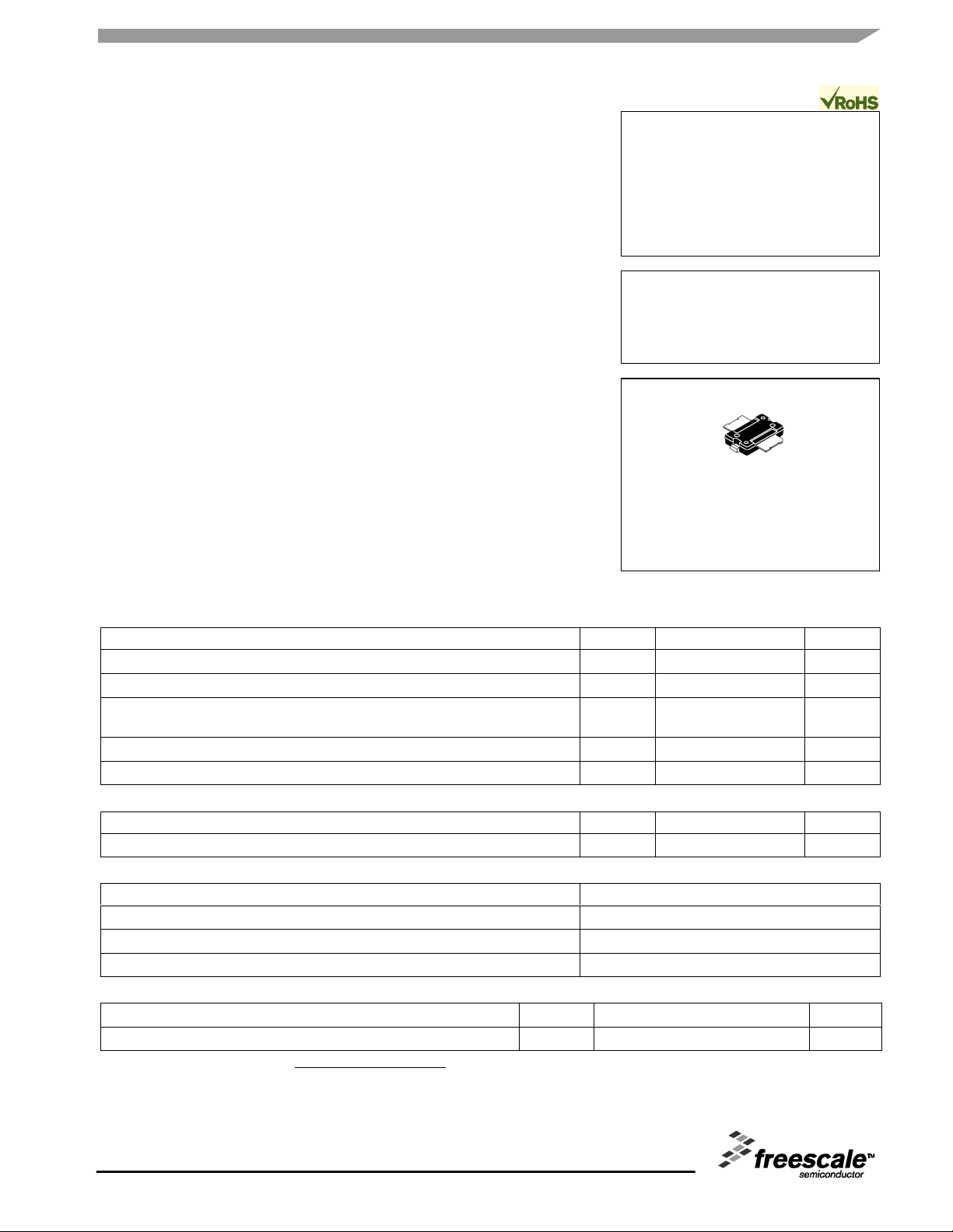
RF Power Field Effect Transistor
N-Channel Enhancement - Mode Lateral MOSFET
Document Number: MRF9060N
Rev. 13, 6/2009
Designed for broadband commercial and industrial applications with frequencies up to 1000 MHz. The high gain and broadband performance of this device
make it ideal for large - signal, common-source amplifier applications in 26 volt
N
base station equipment.
• Typical Performance at 945 MHz, 26 Volts
I
R NEW DE
MMENDED F
T RE
N
Output Power — 60 Watts PEP
Power Gain — 18.0 dB
Efficiency — 40% (Two Tones)
IMD — - 31.5 dBc
• Capable of Handling 5:1 VSWR, @ 26 Vdc, 945 MHz, 60 Watts CW
Output Power
Features
• Excellent Thermal Stability
• Characterized with Series Equivalent Large - Signal Impedance Parameters
• Integrated ESD Protection
• 200_C Capable Plastic Package
• N Suffix Indicates Lead- Free Terminations. RoHS Compliant.
• TO-270 -2 Available in Tape and Reel. R1 Suffix = 500 Units per 24 mm,
13 inch Reel.
Table 1. Maximum Ratings
Rating Symbol Value Unit
Drain-Source Voltage V
Gate- Source Voltage V
Total Device Dissipation @ TC = 25°C
Derate above 25°C
Storage Temperature Range T
Operating Junction Temperature T
Table 2. Thermal Characteristics
Characteristic Symbol Value
Thermal Resistance, Junction to Case R
Table 3. ESD Protection Characteristics
Test Conditions Class
Human Body Model 1 (Minimum)
Machine Model M2 (Minimum)
Charge Device Model C6 (Minimum)
Table 4. Moisture Sensitivity Level
Test Methodology Rating Package Peak Temperature Unit
Per JESD22-A113, IPC/JEDEC J- STD -020 3 260 °C
1. MTTF calculator available at http://www.freescale.com/rf. Select Software & Tools/Development Tools/Calculators to access MTTF
calculators by product.
DSS
GS
P
stg
θ
D
J
JC
MRF9060NR1
945 MHz, 60 W, 26 V
LATERAL N - CHANNEL
BROADBAND
RF POWER MOSFET
CASE 1265-09, STYLE 1
TO-270- 2
PLASTIC
- 0.5, +65 Vdc
- 0.5, +15 Vdc
223
1.79
- 65 to +150 °C
200 °C
(1)
0.56 °C/W
W
W/°C
Unit
NOT RECOMMENDED FOR NEW DESIGN
Freescale Semiconductor, Inc., 2008- 2009. All rights reserved.
RF Device Data
Freescale Semiconductor
MRF9060NR1
1
Page 2
O
CO
O
S
G
Table 5. Electrical Characteristics
Characteristic Symbol Min Typ Max Unit
Off Characteristics
Zero Gate Voltage Drain Leakage Current
(VDS = 65 Vdc, VGS = 0 Vdc)
Zero Gate Voltage Drain Leakage Current
(VDS = 26 Vdc, VGS = 0 Vdc)
N
Gate- Source Leakage Current
= 5 Vdc, VDS = 0 Vdc)
(V
I
R NEW DE
MMENDED F
T RE
N
GS
On Characteristics
Gate Threshold Voltage
(VDS = 10 Vdc, ID = 200 µAdc)
Gate Quiescent Voltage
(VDS = 26 Vdc, ID = 450 mAdc)
Drain-Source On - Voltage
(VGS = 10 Vdc, ID = 1.3 Adc)
Forward Transconductance
(VDS = 10 Vdc, ID = 4 Adc)
Dynamic Characteristics
Input Capacitance
(VDS = 26 Vdc ± 30 mV(rms)ac @ 1 MHz, VGS = 0 Vdc)
Output Capacitance
(VDS = 26 Vdc ± 30 mV(rms)ac @ 1 MHz, VGS = 0 Vdc)
Reverse Transfer Capacitance
(VDS = 26 Vdc ± 30 mV(rms)ac @ 1 MHz, VGS = 0 Vdc)
Functional Tests (In Freescale Test Fixture, 50 ohm system)
Two- Tone Common- Source Amplifier Power Gain
(VDD = 26 Vdc, P
f1 = 945.0 MHz, f2 = 945.1 MHz)
Two- Tone Drain Efficiency
(VDD = 26 Vdc, P
f1 = 945.0 MHz, f2 = 945.1 MHz)
3rd Order Intermodulation Distortion
(VDD = 26 Vdc, P
f1 = 945.0 MHz, f2 = 945.1 MHz)
Input Return Loss
(VDD = 26 Vdc, P
f1 = 945.0 MHz, f2 = 945.1 MHz)
Two- Tone Common- Source Amplifier Power Gain
(VDD = 26 Vdc, P
f1 = 930.0 MHz, f2 = 930.1 MHz and f1 = 960.0 MHz,
f2 = 960.1 MHZ)
Two- Tone Drain Efficiency
(VDD = 26 Vdc, P
f1 = 930.0 MHz, f2 = 930.1 MHz and f1 = 960.0 MHz,
f2 = 960.1 MHZ)
3rd Order Intermodulation Distortion
(VDD = 26 Vdc, P
f1 = 930.0 MHz, f2 = 930.1 MHz and f1 = 960.0 MHz,
f2 = 960.1 MHZ)
Input Return Loss
(VDD = 26 Vdc, P
f1 = 930.0 MHz, f2 = 930.1 MHz and f1 = 960.0 MHz,
f2 = 960.1 MHZ)
= 60 W PEP, IDQ = 450 mA,
out
= 60 W PEP, IDQ = 450 mA,
out
= 60 W PEP, IDQ = 450 mA,
out
= 60 W PEP, IDQ = 450 mA,
out
= 60 W PEP, IDQ = 450 mA,
out
= 60 W PEP, IDQ = 450 mA,
out
= 60 W PEP, IDQ = 450 mA,
out
= 60 W PEP, IDQ = 450 mA,
out
(TA = 25°C unless otherwise noted)
I
DSS
I
DSS
I
GSS
V
GS(th)
V
GS(Q)
V
DS(on)
g
fs
C
iss
C
oss
C
rss
G
ps
η 37 40 — %
IMD — - 31.5 -28 dBc
IRL — - 14.5 -9 dB
G
ps
η — 40 — %
IMD — -31 — dBc
IRL — - 12.5 — dB
— — 10 µAdc
— — 1 µAdc
— — 1 µAdc
2 2.8 4 Vdc
3 3.7 5 Vdc
— 0.21 0.4 Vdc
— 5.3 — S
— 101 — pF
— 53 — pF
— 2.5 — pF
17 18 — dB
— 18 — dB
NOT RECOMMENDED FOR NEW DESIGN
2
MRF9060NR1
RF Device Data
Freescale Semiconductor
Page 3
O
CO
O
S
G
V
N
I
GG
RF
INPUT
+
C6
Z1 Z3 Z7
C1
C7
Z4Z2
C2
L1
Z8 Z9
C3
C5
B2B1
+
+
L2
C9C4
Z11
DUT
Z10Z5 Z6
C8
C14 C16
Z14Z13Z12
C15
Z15 Z17
Z16
C10 C11 C12
C13
V
DD
+
C17
RF
OUTPUT
Z18
Z1 0.240″ x 0.060″ Microstrip
Z2 0.240″ x 0.060″ Microstrip
Z3 0.500″ x 0.100″ Microstrip
Z4 0.100″ x 0.270″ x 0.080″, Taper
Z5 0.330″ x 0.270″ Microstrip
Z6 0.120″ x 0.270″ Microstrip
Z7 0.270″ x 0.520″ x 0.140″, Taper
Z8 0.240″ x 0.520″ Microstrip
Z9 0.340″ x 0.520″ Microstrip
Figure 1. 930- 960 MHz Broadband Test Circuit Schematic
Table 6. 930 - 960 MHz Broadband Test Circuit Component Designations and Values
R NEW DE
Part Description Part Number Manufacturer
B1 Short Ferrite Bead 2743019447 Fair-Rite
B2 Long Ferrite Bead 2743029446 Fair- Rite
C1, C7, C13, C14 47 pF Chip Capacitors ATC100B470JT500XT ATC
C2, C3, C11 0.8- 8.0 Gigatrim Variable Capacitors 27291SL Johanson
C4, C5 11 pF Chip Capacitors (MRF9060NR1)
C6, C15, C16
C8, C9 10 pF Chip Capacitors ATC100B100JT500XT Newark
C10 3.9 pF Chip Capacitor ATC100B3R9CT500XT ATC
C12 1.7 pF Chip Capacitor ATC100B1R7BT500XT ATC
C17
L1, L2 12.5 nH Inductors A04T- 5 Coilcraft
Board Material 30 mil Glass Teflon, εr = 2.55 Copper Clad, 2 oz Cu RF -35- 0300 Taconic
10 pF Chip Capacitors (MRF9060NBR1)
10 mF, 35 V Tantalum Chip Capacitors
220 mF Electrolytic Chip Capacitor
Z10 0.060″ x 0.520″ Microstrip
Z11 0.360″ x 0.270″ Microstrip
Z12 0.060″ x 0.270″ Microstrip
Z13 0.130″ x 0.060″ Microstrip
Z14 0.300″ x 0.060″ Microstrip
Z15 0.210″ x 0.060″ Microstrip
Z16 0.600″ x 0.060″ Microstrip
Z17 0.290″ x 0.060″ Microstrip
Z18 0.340″ x 0.060″ Microstrip
ATC100B110JT500XT
ATC100B100JT500XT
T491D106K035AT Kemet
MCAX63V227M13X22 Multicomp
ATC
MMENDED F
T RE
N
RF Device Data
Freescale Semiconductor
NOT RECOMMENDED FOR NEW DESIGN
MRF9060NR1
3
Page 4
O
CO
O
S
G
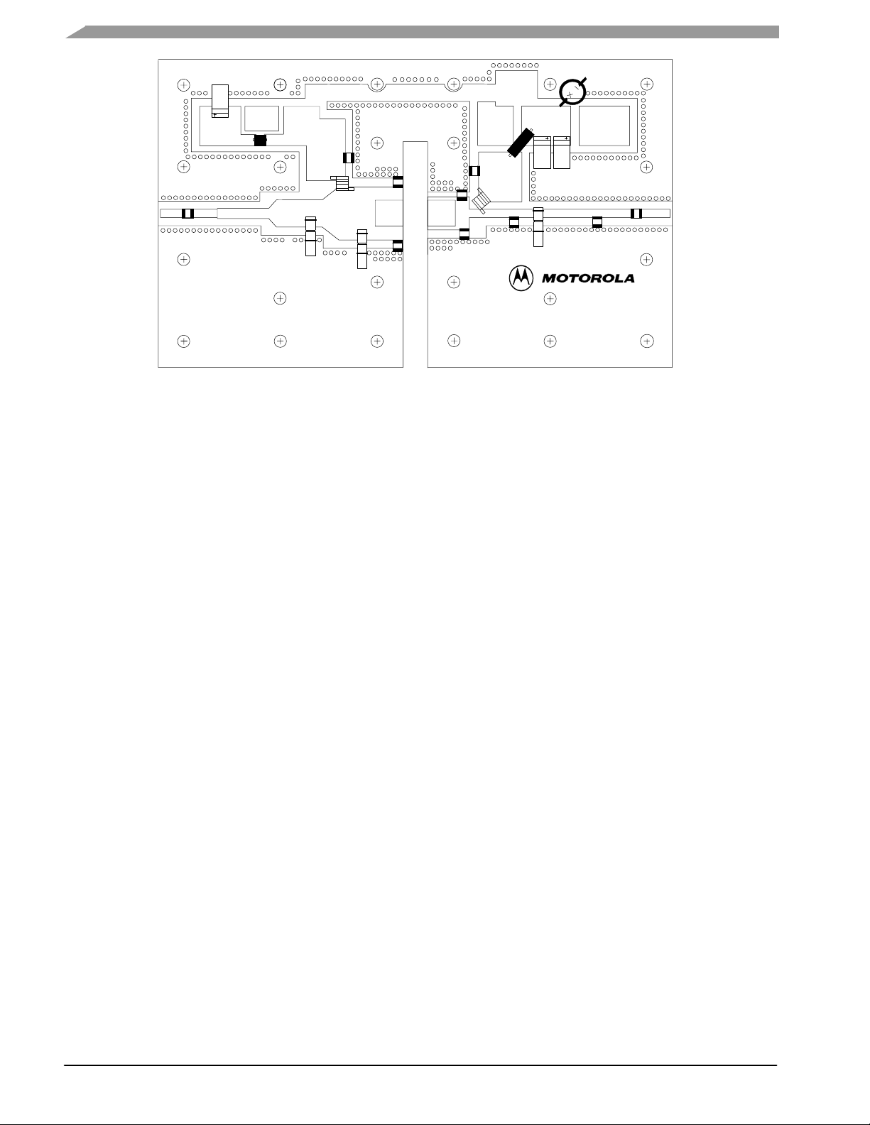
N
I
INPUT
C1
C6
V
GG
B1
C2
C7
B2
C14
WB1
C4
WB2
L1
C3
L2
C8
C9
V
DD
C15 C16
C10C5C11 C12 C13
C17
OUTPUT
Freescale has begun the transition of marking Printed Circuit Boards (PCBs) with the Freescale Semiconductor
signature/logo. PCBs may have either Motorola or Freescale markings during the transition period. These changes will have
no impact on form, fit or function of the current product.
R NEW DE
CUT OUT AREA
Figure 2. 930- 960 MHz Broadband Test Circuit Component Layout
MRF9060M
MRF9060MB
MMENDED F
T RE
N
MRF9060NR1
4
NOT RECOMMENDED FOR NEW DESIGN
RF Device Data
Freescale Semiconductor
Page 5

O
CO
O
S
G
TYPICAL CHARACTERISTICS
N
I
19
IDQ = 625 mA
18.5
R NEW DE
18
17.5
, POWER GAIN (dB)
ps
G
17
16.5
Figure 4. Power Gain versus Output Power Figure 5. Intermodulation Distortion versus
500 mA
450 mA
275 mA
P
, OUTPUT POWER (WATTS) PEP
out
, POWER GAIN (dB)
ps
G
101 100
19
G
18 45
17 40
16 35
15
14
13
12
11
Figure 3. Class AB Broadband Circuit Performance
VDD = 26 Vdc
P
I
DQ
Two−Tone, 100 kHz Tone Spacing
VDD = 26 Vdc
f1 = 945 MHz
f2 = 945.1 MHz
ps
η
= 60 W (PEP)
out
= 450 mA
IMD
IRL
f, FREQUENCY (MHz)
100
955950945940935930
−15
−20
−25
−30
−35
−40
−45
INTERMODULATION DISTORTION (dBc)IMD,
−50
−55
110
960
IDQ = 275 mA
450 mA
500 mA
P
, OUTPUT POWER (WATTS) PEP
out
50
, DRAINη
EFFICIENCY (%)
−28
−30
−32
−34
DISTORTION (dBc)
IMD, INTERMODULATION
−36
625 mA
Output Power
−10
−12
−14
−16
−18
LOSS (dB)
IRL, INPUT RETURN
VDD = 26 Vdc
f1 = 945 MHz
f2 = 945.1 MHz
−10
MMENDED F
−20
−30
−40
−50
−60
T RE
INTERMODULATION DISTORTION (dBc)IMD,
−70
−80
N
RF Device Data
Freescale Semiconductor
VDD = 26 Vdc
IDQ = 450 mA
f1 = 945 MHz
f2 = 945.1 MHz
110
P
out
Figure 6. Intermodulation Distortion Products
3rd Order
5th Order
7th Order
, OUTPUT POWER (WATTS) PEP
versus Output Power
100
20
G
18 50
16 40
14 30
12 20
, POWER GAIN (dB)
ps
G
10 10
8
0.1
P
out
Figure 7. Power Gain and Efficiency versus
ps
η
110
, OUTPUT POWER (WATTS) AVG.
Output Power
VDD = 26 Vdc
IDQ = 450 mA
f = 945 MHz
MRF9060NR1
100
60
, DRAIN EFFICIENCY (%)η
0
NOT RECOMMENDED FOR NEW DESIGN
5
Page 6

O
CO
O
S
G
TYPICAL CHARACTERISTICS
N
I
R NEW DE
20
G
18 40
16 20
14 0
VDD = 26 Vdc
IDQ = 450 mA
12
, POWER GAIN (dB)
f1 = 945 MHz
ps
G
f2 = 945.1 MHz
10
8
110
Figure 8. Power Gain, Efficiency, and IMD versus Output Power
11
10
)
2
10
10
ps
η
IMD
P
, OUTPUT POWER (WATTS) PEP
out
100
60
−20
−40
−60
INTERMODULATION DISTORTION (dBc)IMD,
, DRAIN EFFICIENCY (%)η
MMENDED F
T RE
N
9
10
MTTF FACTOR (HOURS X AMPS
8
10
90 110 130 150 170 190100 120 140 160 180 200
TJ, JUNCTION TEMPERATURE (°C)
This above graph displays calculated MTTF in hours x ampere
drain current. Life tests at elevated temperatures have correlated to
better than ±10% of the theoretical prediction for metal failure. Divide
MTTF factor by I
Figure 9. MTTF Factor versus Junction Temperature
2
for MTTF in a particular application.
D
2
210
NOT RECOMMENDED FOR NEW DESIGN
MRF9060NR1
6
RF Device Data
Freescale Semiconductor
Page 7

O
CO
O
S
G
N
I
R NEW DE
Z
MMENDED F
Z
f = 930 MHz
f = 960 MHz
Z
source
VDD = 26 V, IDQ = 450 mA, P
f
MHz
930
945
960
= Test circuit impedance as measured from
source
= Test circuit impedance as measured
load
Z
source
Ω
0.63 + j0.57
0.60 + j0.41
0.57 + j0.45
gate to ground.
from drain to ground.
Zo = 2 Ω
= 60 W PEP
out
Z
load
f = 960 MHz
Z
load
Ω
1.8 + j0.84
1.7 + j0.55
1.6 + j0.36
f = 930 MHz
T RE
N
RF Device Data
Freescale Semiconductor
Output
Matching
Network
Z
source
Device
Under
Test
Z
load
Input
Matching
Network
Figure 10. Series Equivalent Source and Load Impedance
NOT RECOMMENDED FOR NEW DESIGN
MRF9060NR1
7
Page 8

O
CO
O
S
G
N
I
R NEW DE
PACKAGE DIMENSIONS
MMENDED F
T RE
N
MRF9060NR1
8
NOT RECOMMENDED FOR NEW DESIGN
RF Device Data
Freescale Semiconductor
Page 9

O
CO
O
S
G
N
I
R NEW DE
MMENDED F
T RE
N
RF Device Data
Freescale Semiconductor
NOT RECOMMENDED FOR NEW DESIGN
MRF9060NR1
9
Page 10

O
CO
O
S
G
N
I
R NEW DE
MMENDED F
T RE
N
MRF9060NR1
10
NOT RECOMMENDED FOR NEW DESIGN
RF Device Data
Freescale Semiconductor
Page 11

O
CO
O
S
G
PRODUCT DOCUMENTATION, TOOLS AND SOFTWARE
Refer to the following documents to aid your design process.
Application Notes
• AN1907: Solder Reflow Attach Method for High Power RF Devices in Plastic Packages
• AN1955: Thermal Measurement Methodology of RF Power Amplifiers
• AN3789: Clamping of High Power RF Transistors and RFICs in Over- Molded Plastic Packages
N
Engineering Bulletins
• EB212: Using Data Sheet Impedances for RF LDMOS Devices
Software
I
• Electromigration MTTF Calculator
For Software and Tools, do a Part Number search at http://www.freescale.com, and select the “Part Number” link. Go to the
Software & Tools tab on the part’s Product Summary page to download the respective tool.
REVISION HISTORY
The following table summarizes revisions to this document.
Revision Date Description
12 Sept. 2008 • Data sheet revised to reflect part status change, p. 1, including use of applicable overlay.
R NEW DE
13 June 2009 • Modified data sheet to reflect MSL rating change from 1 to 3 as a result of the standardization of packing
• Replaced Case Outline 1265-08 with 1265-09, Issue K, p. 1, 8- 10. Corrected cross hatch pattern in
bottom view and changed its dimensions (D2 and E3) to minimum value on source contact (D2 changed
from Min- Max .290 - .320 to .290 Min; E3 changed from Min -Max .150- .180 to .150 Min). Added JEDEC
Standard Package Number.
• Updated Part Numbers in Table 6, Component Designations and Values, to RoHS compliant part
numbers, p. 3
• Added Product Documentation and Revision History, p. 11
process as described in Product and Process Change Notification number, PCN13516, p. 1
• Added Electromigration MTTF Calculator availability to Product Documentation, Tools and Software, p. 11
MMENDED F
T RE
N
RF Device Data
Freescale Semiconductor
NOT RECOMMENDED FOR NEW DESIGN
MRF9060NR1
11
Page 12

O
CO
O
S
G
N
I
How to Reach Us:
Home Page:
www.freescale.com
Web Support:
http://www.freescale.com/support
USA/Europe or Locations Not Listed:
Freescale Semiconductor, Inc.
Technical Information Center, EL516
2100 East Elliot Road
Tempe, Arizona 85284
1-800 - 521 - 6274 or +1 -480-768- 2130
www.freescale.com/support
R NEW DE
Europe, Middle East, and Africa:
Freescale Halbleiter Deutschland GmbH
Technical Information Center
Schatzbogen 7
81829 Muenchen, Germany
+44 1296 380 456 (English)
+46 8 52200080 (English)
+49 89 92103 559 (German)
+33 1 69 35 48 48 (French)
www.freescale.com/support
Japan:
Freescale Semiconductor Japan Ltd.
Headquarters
ARCO Tower 15F
1-8 - 1, Shimo - Meguro, Meguro - ku,
Tokyo 153 - 0064
Japan
0120 191014 or +81 3 5437 9125
support.japan@freescale.com
MMENDED F
Asia/Pacific:
Freescale Semiconductor China Ltd.
Exchange Building 23F
No. 118 Jianguo Road
Chaoyang District
Beijing 100022
China
+86 10 5879 8000
support.asia@freescale.com
For Literature Requests Only:
Freescale Semiconductor Literature Distribution Center
T RE
1-800 - 441 - 2447 or +1 -303-675- 2140
Fax: +1-303 - 675 - 2150
LDCForFreescaleSemiconductor@hibbertgroup.com
Information in this document is provided solely to enable system and software
implementers to use Freescale Semiconductor products. There are no express or
implied copyright licenses granted hereunder to design or fabricate any integrated
circuits or integrated circuits based on the information in this document.
Freescale Semiconductor reserves the right to make changes without further notice to
any products herein. Freescale Semiconductor makes no warranty, representation or
guarantee regarding the suitability of its products for any particular purpose, nor does
Freescale Semiconductor assume any liability arising out of the application or use of
any product or circuit, and specifically disclaims any and all liability, including without
limitation consequential or incidental damages. “Typical” parameters that may be
provided in Freescale Semiconductor data sheets and/or specifications can and do
vary in different applications and actual performance may vary over time. All operating
parameters, including “Typicals”, must be validated for each customer application by
customer’s technical experts. Freescale Semiconductor does not convey any license
under its patent rights nor the rights of others. Freescale Semiconductor products are
not designed, intended, or authorized for use as components in systems intended for
surgical implant into the body, or other applications intended to support or sustain life,
or for any other application in which the failure of the Freescale Semiconductor product
could create a situation where personal injury or death may occur. Should Buyer
purchase or use Freescale Semiconductor products for any such unintended or
unauthorized application, Buyer shall indemnify and hold Freescale Semiconductor
and its officers, employees, subsidiaries, affiliates, and distributors harmless against all
claims, costs, damages, and expenses, and reasonable attorney fees arising out of,
directly or indirectly, any claim of personal injury or death associated with such
unintended or unauthorized use, even if such claim alleges that Freescale
Semiconductor was negligent regarding the design or manufacture of the part.
Freescalet and the Freescale logo are trademarks of Freescale Semiconductor, Inc.
All other product or service names are the property of their respective owners.
Freescale Semiconductor, Inc. 2008- 2009. All rights reserved.
N
MRF9060NR1
Document Number: MRF9060N
Rev. 13, 6/2009
12
NOT RECOMMENDED FOR NEW DESIGN
RoHS-compliant and/or Pb -free versions of Freescale products have the functionality and electrical
characteristics of their non-RoHS- compliant and/or non- Pb - free counterparts. For further
information, see http://www.freescale.com or contact your Freescale sales representative.
For information on Freescale’s Environmental Products program, go to http://www.freescale.com/epp.
RF Device Data
Freescale Semiconductor
 Loading...