

Page 1
www.DataSheet4U.com
Freescale Semiconductor
Technical Data
RF Power Field Effect Transistor
N-Channel Enhancement - Mode Lateral MOSFETs
Designed primarily for CW large -signal output and driver applications with
frequencies up to 450 MHz. Devices are unmatched and are suitable for use in
industrial, medical and scientific applications.
• Typical CW Performance at 220 MHz: VDD = 50 Volts, IDQ = 30 mA,
= 10 Watts
P
out
Power Gain — 23.9 dB
Drain Efficiency — 62%
• Capable of Handling 10:1 VSWR, @ 50 Vdc, 220 MHz, 10 Watts CW
Output Power
Features
• Integrated ESD Protection
• Excellent Thermal Stability
• Facilitates Manual Gain Control, ALC and Modulation Techniques
• 200°C Capable Plastic Package
• RoHS Compliant
• TO-270 - 2 in Tape and Reel. R1 Suffix = 500 Units per 24 mm,
13 inch Reel.
• TO-272 - 2 in Tape and Reel. R1 Suffix = 500 Units per 44 mm,
13 inch Reel.
Document Number: MRF6V2010N
Rev. 1, 5/2007
MRF6V2010NR1
MRF6V2010NBR1
10- 450 MHz, 10 W, 50 V
LATERAL N - CHANNEL
BROADBAND
RF POWER MOSFETs
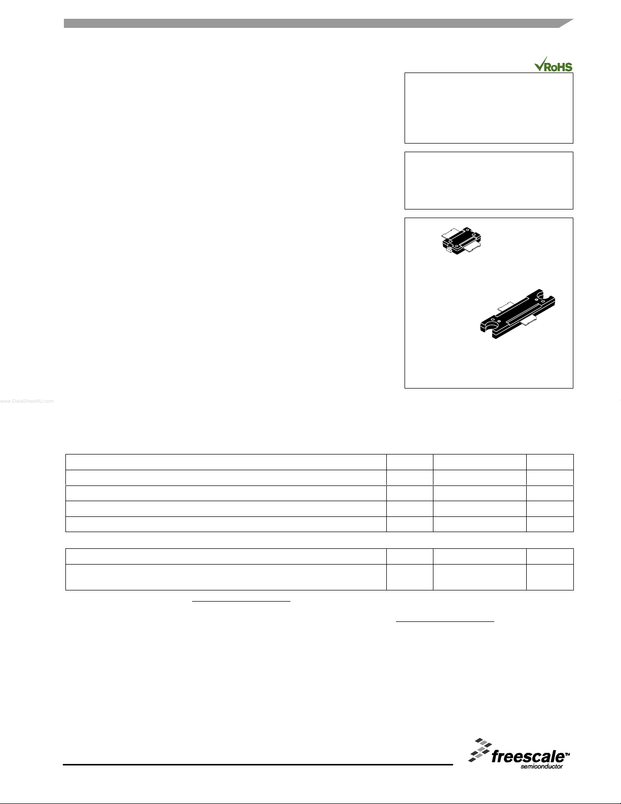
CASE 1265-08, STYLE 1
TO-270-2
PLASTIC
MRF6V2010NR1
CASE 1337-03, STYLE 1
TO-272-2
PLASTIC
MRF6V2010NBR1
Table 1. Maximum Ratings
Rating Symbol Value Unit
Drain-Source Voltage V
Gate-Source Voltage V
Storage Temperature Range T
Operating Junction Temperature T
DSS
GS
stg
J
-0.5, +110 Vdc
-0.5, +10 Vdc
- 65 to +150 °C
200 °C
Table 2. Thermal Characteristics
Characteristic Symbol Value
Thermal Resistance, Junction to Case
Case Temperature 81°C, 10 W CW R
1. MTTF calculator available at http://www.freescale.com/rf. Select Tools/Software/Application Software/Calculators to access the MTTF
calculators by product.
2. Refer to AN1955, Thermal Measurement Methodology of RF Power Amplifiers. Go to http://www.freescale.com/rf.
Select Documentation/Application Notes - AN1955.
θ
JC
(1,2)
3.0 °C/W
Unit
Freescale Semiconductor, Inc., 2007. All rights reserved.
RF Device Data
Freescale Semiconductor
MRF6V2010NR1 MRF6V2010NBR1
1
Page 2
Table 3. ESD Protection Characteristics
Test Methodology Class
Human Body Model (per JESD22-A114) 2 (Minimum)
Machine Model (per EIA/JESD22 - A115) A (Minimum)
Charge Device Model (per JESD22-C101) IV (Minimum)
Table 4. Moisture Sensitivity Level
Test Methodology Rating Package Peak Temperature Unit
Per JESD 22-A113, IPC/JEDEC J- STD - 020 3 260 °C
Table 5. Electrical Characteristics (T
Characteristic Symbol Min Typ Max Unit
Off Characteristics
Zero Gate Voltage Drain Leakage Current
= 100 Vdc, VGS = 0 Vdc)
(V
DS
Zero Gate Voltage Drain Leakage Current
(VDS = 50 Vdc, VGS = 0 Vdc)
Drain-Source Breakdown Voltage
(ID = 5 mA, VGS = 0 Vdc)
Gate-Source Leakage Current
(VGS = 5 Vdc, VDS = 0 Vdc)
On Characteristics
Gate Threshold Voltage
(VDS = 10 Vdc, ID = 28 µAdc)
Gate Quiescent Voltage
(VDD = 50 Vdc, ID = 30 mAdc, Measured in Functional Test)
Drain-Source On-Voltage
(VGS = 10 Vdc, ID = 70 mAdc)
Dynamic Characteristics
Reverse Transfer Capacitance
(VDS = 50 Vdc ± 30 mV(rms)ac @ 1 MHz, VGS = 0 Vdc)
Output Capacitance
(VDS = 50 Vdc ± 30 mV(rms)ac @ 1 MHz, VGS = 0 Vdc)
Input Capacitance
(VDS = 50 Vdc ± 30 mV(rms)ac @ 1 MHz, VGS = 0 Vdc)
Functional Tests (In Freescale Test Fixture, 50 ohm system) VDD = 50 Vdc, IDQ = 30 mA, P
Power Gain G
Drain Efficiency η
Input Return Loss IRL — -14 -9 dB
= 25°C unless otherwise noted)
C
I
DSS
I
DSS
V
(BR)DSS
I
GSS
V
GS(th)
V
GS(Q)
V
DS(on)
C
C
C
rss
oss
iss
ps
D
— — 2.5 mA
— — 50 µAdc
110 — — Vdc
— — 10 µAdc
1 1.68 3 Vdc
1.5 2.68 3.5 Vdc
— 0.26 — Vdc
— 0.13 — pF
— 7.3 — pF
— 16.3 — pF
= 10 W, f = 220 MHz, CW
out
22.5 23.9 25.5 dB
58 62 — %
ATTENTION: The MRF6V2010N and MRF6V2010NB are high power devices and special considerations
must be followed in board design and mounting. Incorrect mounting can lead to internal temperatures which
exceed the maximum allowable operating junction temperature. Refer to Freescale Application Note AN3263
(for bolt down mounting) or AN1907 (for solder reflow mounting) PRIOR TO STARTING SYSTEM DESIGN to
ensure proper mounting of these devices.
MRF6V2010NR1 MRF6V2010NBR1
2
RF Device Data
Freescale Semiconductor
Page 3
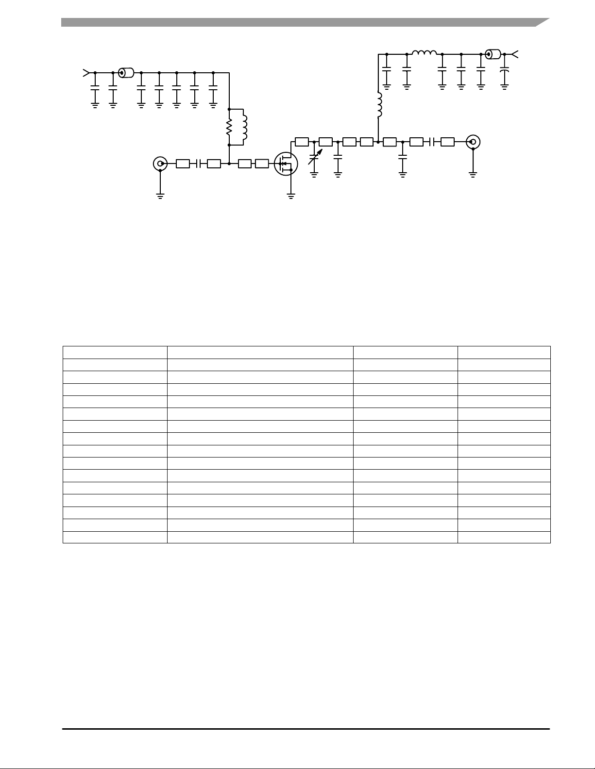
C14 C15
RF
OUTPUT
B2
V
SUPPLY
+
L2
B1
V
BIAS
+
+
C4C2
C5
RF
INPUT
C7C6
C8
L3
R1 L1
Z1
Z2 Z3 Z4
C1
Z5 Z11Z6
DUT
C9 C10
Z7
Z8 Z9
C3
C12 C13C11 C16
Z10
C18
C17
Z1 0.235″ x 0.082″ Microstrip
Z2 1.190″ x 0.082″ Microstrip
Z3 0.619″ x 0.082″ Microstrip
Z4 0.190″ x 0.270″ Microstrip
Z5 0.293″ x 0.270″ Microstrip
Z6 0.120″ x 0.270″ Microstrip
Z7 0.062″ x 0.270″ Microstrip
Z8 0.198″ x 0.082″ Microstrip
Z9 5.600″ x 0.082″ Microstrip
Z10 0.442″ x 0.082″ Microstrip
Z11 0.341″ x 0.082″ Microstrip
PCB Arlon GX- 0300 - 55 - 22, 0.030″, εr = 2.55
Figure 1. MRF6V2010NR1(NBR1) Test Circuit Schematic
Table 6. MRF6V2010NR1(NBR1) Test Circuit Component Designations and Values
Part Description Part Number Manufacturer
B1, B2 95 Ω, 100 MHz Long Ferrite Beads 2743021447 Fair-Rite
C1, C8, C11, C18 1000 pF Chip Capacitors ATC100B102JT50XT ATC
C2 10 µF, 35 V Tantalum Capacitor T491D106K035AT Kemet
C3 22 µF, 35 V Tantalum Capacitor T491X226K035AT Kemet
C4, C13 39 K pF Chip Capacitors ATC200B393KT50XT ATC
C5, C14 22 K pF Chip Capacitors ATC200B223KT50XT ATC
C6, C15 0.1 µF Chip Capacitors CDR33BX104AKYS Kemet
C7, C12 2.2 µF, 50 V Chip Capacitors C1825C225J5RAC Kemet
C9 0.6-4.5 pF Variable Capacitor, Gigatrim 27271SL Johanson
C10 12 pF Chip Capacitor ATC100B120JT500XT ATC
C16 470 µF, 63 V Electrolytic Capacitor ESMG630ELL471MK205 United Chemi-Con
C17 27 pF Chip Capacitor ATC100B270JT500XT ATC
L1 17.5 nH Inductor B06T CoilCraft
L2, L3 82 nH Inductors 1812SMS - 82NJ CoilCraft
R1 120 Ω, 1/4 W Chip Resistor CRCW12061200FKTA Vishay
RF Device Data
Freescale Semiconductor
MRF6V2010NR1 MRF6V2010NBR1
3
Page 4
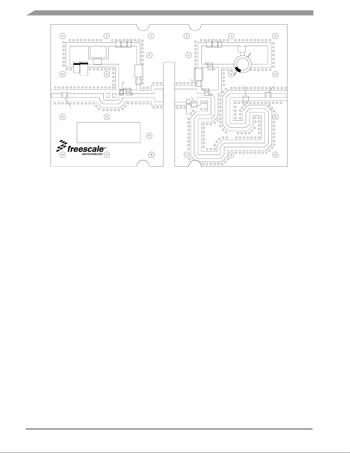
C5
C14
C1
C2
C13
C15
L2
L3
C3
MRF6V2010N/NB
B1
Rev. 3
C4
R1
C6
C7
L1
C8
C12
C11
C10
C9
CUT OUT AREA
Figure 2. MRF6V2010NR1(NBR1) Test Circuit Component Layout
B2
C17
C16
C18
MRF6V2010NR1 MRF6V2010NBR1
4
RF Device Data
Freescale Semiconductor
Page 5
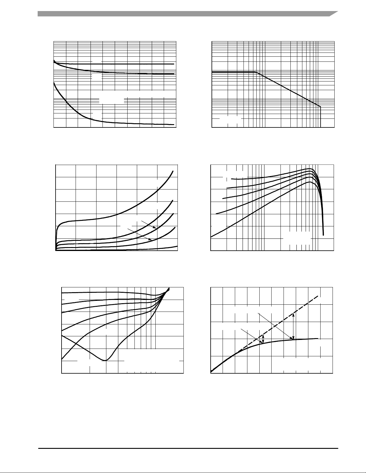
TYPICAL CHARACTERISTICS
100
C
iss
10
C
oss
1
C, CAPACITANCE (pF)
Measured with ±30 mV(rms)ac @ 1 MHz
VGS = 0 Vdc
C
rss
0.1
02010
30
40 100
VDS, DRAIN−SOURCE VOLTAGE (VOLTS)
Figure 3. Capacitance versus Drain-Source Voltage
0.35
0.3
VGS = 3 V
0.25
0.2
2.75 V
0.15
2.63 V
0.1
, DRAIN CURRENT (AMPS)
D
I
0.05
2.5 V
0
0
20 120
40
60
80 100
DRAIN VOLTAGE (VOLTS)
Figure 5. DC Drain Current versus Drain Voltage
2.25 V
100
10
1
, DRAIN CURRENT (AMPS)
D
I
TC = 25°C
0.1
50
1
10
200
VDS, DRAIN−SOURCE VOLTAGE (VOLTS)
Figure 4. DC Safe Operating Area
25
IDQ = 45 mA
24
23
IDQ = 45 mA
38 mA
38 mA
30 mA
22
23 mA
21
, POWER GAIN (dB)
ps
20
15 mA
G
19
VDD = 50 Vdc
f1 = 220 MHz
18
0.1
120
P
, OUTPUT POWER (WATTS) CW
out
10
Figure 6. CW Power Gain versus Output Power
−20
15 mA
23 mA
−25
−30
30 mA
−35
38 mA
−40
DISTORTION (dBc)
−45
IMD, THIRD ORDER INTERMODULATION
−50
−55
IDQ = 60 mA
1
P
out
Figure 7. Third Order Intermodulation Distortion
RF Device Data
Freescale Semiconductor
45 mA
VDD = 50 Vdc
f1 = 220 MHz, f2 = 220.1 MHz
Two− Tone Measurements
100 kHz Tone Spacing
, OUTPUT POWER (WATTS) PEP
versus Output Power
10 20
47
45
P3dB = 40.87 dBm (12.2 W)
43
P1dB = 40.43 dBm (11.04 W)
41
, OUTPUT POWER (dBm)
out
P
39
VDD = 50 Vdc, IDQ = 30 mA
37
13 1715
f = 220 MHz
19 21
Pin, INPUT POWER (dBm)
Figure 8. CW Output Power versus Input Power
MRF6V2010NR1 MRF6V2010NBR1
Ideal
Actual
23
5
Page 6

TYPICAL CHARACTERISTICS
26
24
22
20
18
16
, POWER GAIN (dB)
ps
G
14
12
VDD = 20 V
10
082
Figure 9. Power Gain versus Output Power
26
25
24
TC = −30_C
23
22
21
85_C
, POWER GAIN (dB)
ps
G
20
19
18
0.1
Figure 11. Power Gain and Drain Efficiency
40 V
35 V
30 V
25 V
46
P
, OUTPUT POWER (WATTS) CW
out
G
ps
η
25_C
D
10 12
VDD = 50 Vdc
IDQ = 30 mA
f = 220 MHz
1
P
, OUTPUT POWER (WATTS) CW
out
versus CW Output Power
45 V
IDQ = 30 mA
f = 220 MHz
−30_C
50 V
25_C
85_C
10 20
14
72
63
54
45
36
27
DRAIN EFFICIENCY (%)
18
D,
η
9
0
45
= −30_C
T
C
40
25_C
85_C
35
30
, OUTPUT POWER (dBm)
out
P
25
VDD = 50 Vdc
IDQ = 30 mA
f = 220 MHz
20
0
10 20
155
Pin, INPUT POWER (dBm)
Figure 10. Power Output versus Power Input
8
10
7
10
6
MTTF (HOURS)
10
5
10
90
110 130 150 170 190
TJ, JUNCTION TEMPERATURE (°C)
This above graph displays calculated MTTF in hours when the device
is operated at VDD = 50 Vdc, P
= 10 W CW, and ηD = 62%.
out
MTTF calculator available at http:/www.freescale.com/rf. Select Tools/
Software/Application Software/Calculators to access the MTTF calcu−
lators by product.
210 230
25
250
MRF6V2010NR1 MRF6V2010NBR1
6
Figure 12. MTTF versus Junction Temperature
RF Device Data
Freescale Semiconductor
Page 7

Z
source
Zo = 50 Ω
f = 220 MHz
Z
load
f = 220 MHz
VDD = 50 Vdc, IDQ = 30 mA, P
f
Z
MHz
source
W
= 10 W CW
out
Z
load
W
220 20 + j25 75 + j44
Z
= Test circuit impedance as measured from
source
Z
load
Input
Matching
Network
gate to ground.
= Test circuit impedance as measured
from drain to ground.
Output
Matching
Network
Z
source
Device
Under
Test
Z
load
Figure 13. Series Equivalent Source and Load Impedance
RF Device Data
Freescale Semiconductor
MRF6V2010NR1 MRF6V2010NBR1
7
Page 8

PACKAGE DIMENSIONS
MRF6V2010NR1 MRF6V2010NBR1
8
RF Device Data
Freescale Semiconductor
Page 9

RF Device Data
Freescale Semiconductor
MRF6V2010NR1 MRF6V2010NBR1
9
Page 10

MRF6V2010NR1 MRF6V2010NBR1
10
RF Device Data
Freescale Semiconductor
Page 11

RF Device Data
Freescale Semiconductor
MRF6V2010NR1 MRF6V2010NBR1
11
Page 12

MRF6V2010NR1 MRF6V2010NBR1
12
RF Device Data
Freescale Semiconductor
Page 13

RF Device Data
Freescale Semiconductor
MRF6V2010NR1 MRF6V2010NBR1
13
Page 14

PRODUCT DOCUMENTATION
Refer to the following documents to aid your design process.
Application Notes
• AN1907: Solder Reflow Attach Method for High Power RF Devices in Plastic Packages
• AN1955: Thermal Measurement Methodology of RF Power Amplifiers
• AN3263: Bolt Down Mounting Method for High Power RF Transistors and RFICs in Over-Molded Plastic Packages
Engineering Bulletins
• EB212: Using Data Sheet Impedances for RF LDMOS Devices
REVISION HISTORY
The following table summarizes revisions to this document.
Revision Date Description
0 Feb. 2007 • Initial Release of Data Sheet
1 May 2007 • Corrected Test Circuit Component part numbers in Table 6, Component Designations and Values for C1,
C8, C11, C18, C4, C13, C5, and C14, p. 3
• Corrected Series Impedance Z
Impedance, p. 7
source
and Z
values, Fig. 13, Series Equivalent Source and Load
load
MRF6V2010NR1 MRF6V2010NBR1
14
RF Device Data
Freescale Semiconductor
Page 15

How to Reach Us:
Home Page:
www.freescale.com
Web Support:
http://www.freescale.com/support
USA/Europe or Locations Not Listed:
Freescale Semiconductor, Inc.
Technical Information Center, EL516
2100 East Elliot Road
Tempe, Arizona 85284
+1-800-521-6274 or +1-480-768-2130
www.freescale.com/support
Europe, Middle East, and Africa:
Freescale Halbleiter Deutschland GmbH
Technical Information Center
Schatzbogen 7
81829 Muenchen, Germany
+44 1296 380 456 (English)
+46 8 52200080 (English)
+49 89 92103 559 (German)
+33 1 69 35 48 48 (French)
www.freescale.com/support
Japan:
Freescale Semiconductor Japan Ltd.
Headquarters
ARCO Tower 15F
1-8-1, Shimo-Meguro, Meguro-ku,
Tokyo 153 - 0064
Japan
0120 191014 or +81 3 5437 9125
support.japan@freescale.com
Asia/Pacific:
Freescale Semiconductor Hong Kong Ltd.
Technical Information Center
2 Dai King Street
Tai Po Industrial Estate
Tai Po, N.T., Hong Kong
+800 2666 8080
support.asia@freescale.com
For Literature Requests Only:
Freescale Semiconductor Literature Distribution Center
P.O. Box 5405
Denver, Colorado 80217
1-800-441-2447 or 303-675-2140
Fax: 303-675-2150
LDCForFreescaleSemiconductor@hibbertgroup.com
Information in this document is provided solely to enable system and software
implementers to use Freescale Semiconductor products. There are no express or
implied copyright licenses granted hereunder to design or fabricate any integrated
circuits or integrated circuits based on the information in this document.
Freescale Semiconductor reserves the right to make changes without further notice to
any products herein. Freescale Semiconductor makes no warranty, representation or
guarantee regarding the suitability of its products for any particular purpose, nor does
Freescale Semiconductor assume any liability arising out of the application or use of
any product or circuit, and specifically disclaims any and all liability, including without
limitation consequential or incidental damages. “Typical” parameters that may be
provided in Freescale Semiconductor data sheets and/or specifications can and do
vary in different applications and actual performance may vary over time. All operating
parameters, including “Typicals”, must be validated for each customer application by
customer’s technical experts. Freescale Semiconductor does not convey any license
under its patent rights nor the rights of others. Freescale Semiconductor products are
not designed, intended, or authorized for use as components in systems intended for
surgical implant into the body, or other applications intended to support or sustain life,
or for any other application in which the failure of the Freescale Semiconductor product
could create a situation where personal injury or death may occur. Should Buyer
purchase or use Freescale Semiconductor products for any such unintended or
unauthorized application, Buyer shall indemnify and hold Freescale Semiconductor
and its officers, employees, subsidiaries, affiliates, and distributors harmless against all
claims, costs, damages, and expenses, and reasonable attorney fees arising out of,
directly or indirectly, any claim of personal injury or death associated with such
unintended or unauthorized use, even if such claim alleges that Freescale
Semiconductor was negligent regarding the design or manufacture of the part.
Freescalet and the Freescale logo are trademarks of Freescale Semiconductor, Inc.
All other product or service names are the property of their respective owners.
Freescale Semiconductor, Inc. 2007. All rights reserved.
Document Number: MRF6V2010N
RF Device Data
Rev. 1, 5/2007
Freescale Semiconductor
MRF6V2010NR1 MRF6V2010NBR1
15
 Loading...