

Freescale Semiconductor
Technical Data
RF Power Field Effect Transistors
N-Channel Enhancement - Mode Lateral MOSFETs
Designed for CDMA base station applications with frequencies from 2300 to
2400 MHz. Suitable for WiMAX, WiBro and multicarrier amplifier applications.
To be used in Class AB and Class C WLL applications.
• Typical 2-Carrier W - CDMA Performance: VDD = 28 Volts, IDQ = 1300 mA,
P
= 28 Watts Avg., f = 2390 MHz, Channel Bandwidth = 3.84 MHz,
out
PAR = 8.5 dB @ 0.01% Probability on CCDF.
Power Gain — 15.2 dB
Drain Efficiency — 25%
IM3 @ 10 MHz Offset — - 37 dBc in 3.84 MHz Channel Bandwidth
ACPR @ 5 MHz Offset — - 40 dBc in 3.84 MHz Channel Bandwidth
• Capable of Handling 10:1 VSWR, @ 32 Vdc, 2390 MHz, 140 Watts CW
Output Power
Features
• Characterized with Series Equivalent Large - Signal Impedance Parameters
• Internally Matched for Ease of Use
• Qualified Up to a Maximum of 32 V
• Integrated ESD Protection
• Designed for Lower Memory Effects and Wide Instantaneous Bandwidth
Applications
• RoHS Compliant
• In Tape and Reel. R3 Suffix = 250 Units per 56 mm, 13 inch Reel.
Operation
DD
Document Number: MRF6S23140H
Rev. 2, 12/2008
MRF6S23140HR3
MRF6S23140HSR3
2300 - 2400 MHz, 28 W AVG., 28 V
2 x W- CDMA
LATERAL N - CHANNEL
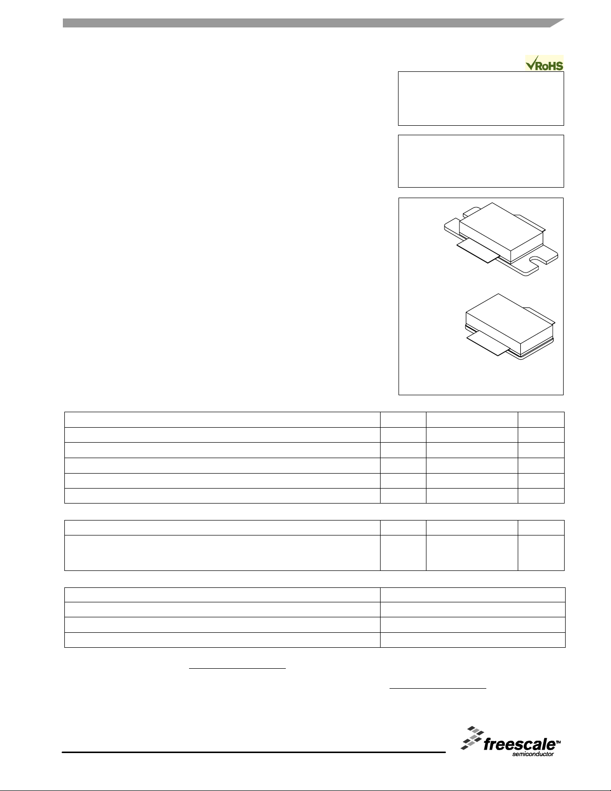
RF POWER MOSFETs
CASE 465B- 03, STYLE 1
NI-880
MRF6S23140HR3
CASE 465C-02, STYLE 1
NI-880S
MRF6S23140HSR3
Table 1. Maximum Ratings
Rating Symbol Value Unit
Drain-Source Voltage V
Gate- Source Voltage V
Storage Temperature Range T
Case Operating Temperature T
Operating Junction Temperature
(1,2)
DSS
GS
stg
C
T
J
-0.5, +68 Vdc
-0.5, +12 Vdc
- 65 to +150 °C
150 °C
225 °C
Table 2. Thermal Characteristics
Characteristic Symbol Value
Thermal Resistance, Junction to Case
Case Temperature 82°C, 140 W CW
Case Temperature 75°C, 28 W CW
R
θ
JC
(2,3)
0.29
0.33
Table 3. ESD Protection Characteristics
Test Methodology Class
Human Body Model (per JESD22-A114) 2 (Minimum)
Machine Model (per EIA/JESD22-A115) A (Minimum)
Charge Device Model (per JESD22-C101) IV (Minimum)
1. Continuous use at maximum temperature will affect MTTF.
2. MTTF calculator available at http://www.freescale.com/rf. Select Software & Tools/Development Tools/Calculators to access
MTTF calculators by product.
3. Refer to AN1955, Thermal Measurement Methodology of RF Power Amplifiers. Go to http://www.freescale.com/rf.
Select Documentation/Application Notes - AN1955.
Unit
°C/W
Freescale Semiconductor, Inc., 2006, 2008. All rights reserved.
RF Device Data
Freescale Semiconductor
MRF6S23140HR3 MRF6S23140HSR3
1
Table 4. Electrical Characteristics
(TC = 25°C unless otherwise noted)
Characteristic Symbol Min Typ Max Unit
Off Characteristics
Zero Gate Voltage Drain Leakage Current
I
DSS
— — 10 µAdc
(VDS = 68 Vdc, VGS = 0 Vdc)
Zero Gate Voltage Drain Leakage Current
I
DSS
— — 1 µAdc
(VDS = 28 Vdc, VGS = 0 Vdc)
Gate- Source Leakage Current
I
GSS
— — 500 nΑdc
(VGS = 5 Vdc, VDS = 0 Vdc)
On Characteristics
Gate Threshold Voltage
V
GS(th)
1 2 3 Vdc
(VDS = 10 Vdc, ID = 300 µAdc)
Gate Quiescent Voltage
V
GS(Q)
2 2.8 4 Vdc
(VDD = 28 Vdc, ID = 1300 mAdc, Measured in Functional Test)
Drain-Source On - Voltage
V
DS(on)
0.1 0.21 0.3 Vdc
(VGS = 10 Vdc, ID = 3 Adc)
Dynamic Characteristics
Reverse Transfer Capacitance
(1)
C
rss
— 2 — pF
(VDS = 28 Vdc ± 30 mV(rms)ac @ 1 MHz, VGS = 0 Vdc)
Functional Tests (In Freescale Test Fixture, 50 ohm system) VDD = 28 Vdc, IDQ = 1300 mA, P
= 28 W Avg., f = 2390 MHz, 2- Carrier
out
W-CDMA, 3.84 MHz Channel Bandwidth Carriers. ACPR measured in 3.84 MHz Channel Bandwidth @ ±5 MHz Offset. IM3 measured in
3.84 MHz Bandwidth @ ±10 MHz Offset. PAR = 8.5 dB @ 0.01% Probability on CCDF.
Power Gain G
Drain Efficiency η
ps
D
13 15.2 17 dB
23 25 — %
Intermodulation Distortion IM3 — -37 -35 dBc
Adjacent Channel Power Ratio ACPR — -40 -38 dBc
Input Return Loss IRL — -15 — dB
1. Part internally matched both on input and output.
MRF6S23140HR3 MRF6S23140HSR3
2
RF Device Data
Freescale Semiconductor
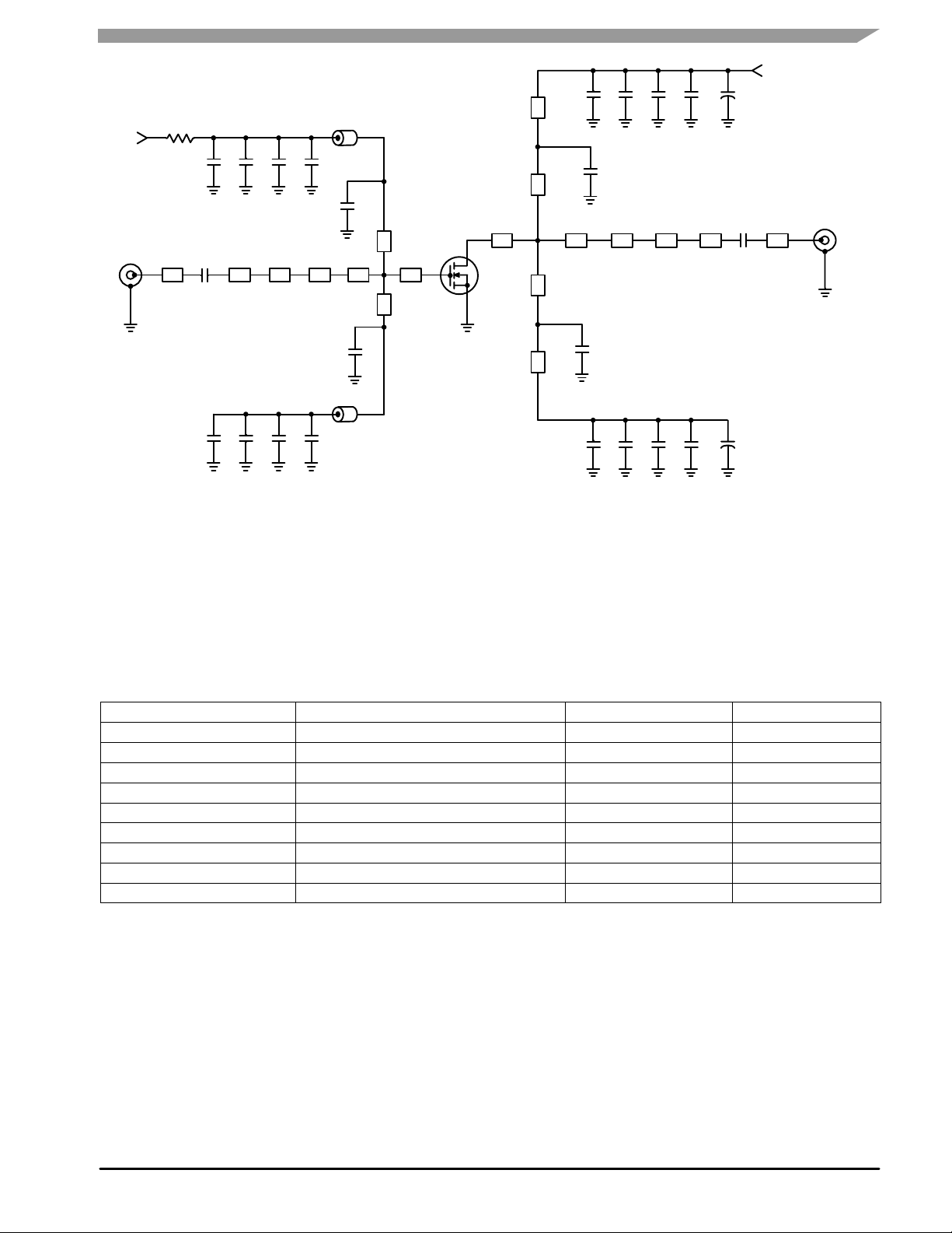
V
BIAS
INPUT
RF
V
SUPPLY
+
Z12
Z11
Z10 Z15 Z16 Z17 Z18
Z13
C9
B1
C3
Z9
Z7
DUT
Z8
R1
+
C11+C10C12
Z1
Z2 Z3 Z4 Z5 Z6
C1
C17 C18C5
C6
C19
C20
RF
OUTPUT
C2
C4
B2
+
C15+C14C16
Z1 0.678″ x 0.068″ Microstrip
Z2 0.420″ x 0.068″ Microstrip
Z3 0.845″ x 0.200″ Microstrip
Z4 0.175″ x 0.530″ Microstrip
Z5, Z6 0.025″ x 0.530″ Microstrip
Z7 0.514″ x 0.050″ Microstrip
Z8 0.507″ x 0.050″ Microstrip
Z9 0.097″ x 1.170″ Microstrip
C13
Z10 0.193″ x 1.170″ Microstrip
Z11, Z13 0.712″ x 0.095″ Microstrip
Z12, Z14 0.098″ x 0.095″ Microstrip
Z15 0.115″ x 0.550″ Microstrip
Z16 0.250″ x 0.110″ Microstrip
Z17 0.539″ x 0.068″ Microstrip
Z18 0.956″ x 0.068″ Microstrip
PCB Taconic RF- 35, 0.030″, εr = 3.5
Z14
C8
+
C21 C22C7
C23
C24
Figure 1. MRF6S23140HR3(SR3) Test Circuit Schematic
Table 5. MRF6S23140HR3(SR3) Test Circuit Component Designations and Values
Part Description Part Number Manufacturer
B1, B2 Ferrite Beads, Short 2743019447 Fair-Rite
C1, C2, C3, C4, C5, C6, C7, C8 5.6 pF Chip Capacitors ATC100B5R6CT500XT ATC
C9, C13 0.01 µF, 100 V Chip Capacitors C1825C103J1RAC Kemet
C10, C14, C17, C21 2.2 µF, 50 V Chip Capacitors C1825C225J5RAC Kemet
C11, C15 22 µF, 25 V Tantalum Chip Capacitors T491D226K025AT Kemet
C12, C16 47 µF, 16 V Tantalum Chip Capacitors T491D476K016AT Kemet
C18, C19, C22, C23 10 µF, 50 V Chip Capacitors GRM55DR61H106KA88B Murata
C20, C24 330 µF, 63 V Electrolytic Capacitors EMVY630GTR331MMH0S Chemi-Con
R1 10 Ω, 1/4 W Chip Resistor CRCW120610R0FKEA Vishay
RF Device Data
Freescale Semiconductor
MRF6S23140HR3 MRF6S23140HSR3
3
C19C6
* Stacked
R1
C1
C15
C16
C12 C11
C10*
C14*
C13*
C9*
C4
B1
C3
CUT OUT AREA
B2
C5
C17 C18
C21 C22
C7
C8
Figure 2. MRF6S23140HR3(SR3) Test Circuit Component Layout
C20
C2
MRF6S23140H
Rev 3
C24
C23
MRF6S23140HR3 MRF6S23140HSR3
4
RF Device Data
Freescale Semiconductor
TYPICAL CHARACTERISTICS
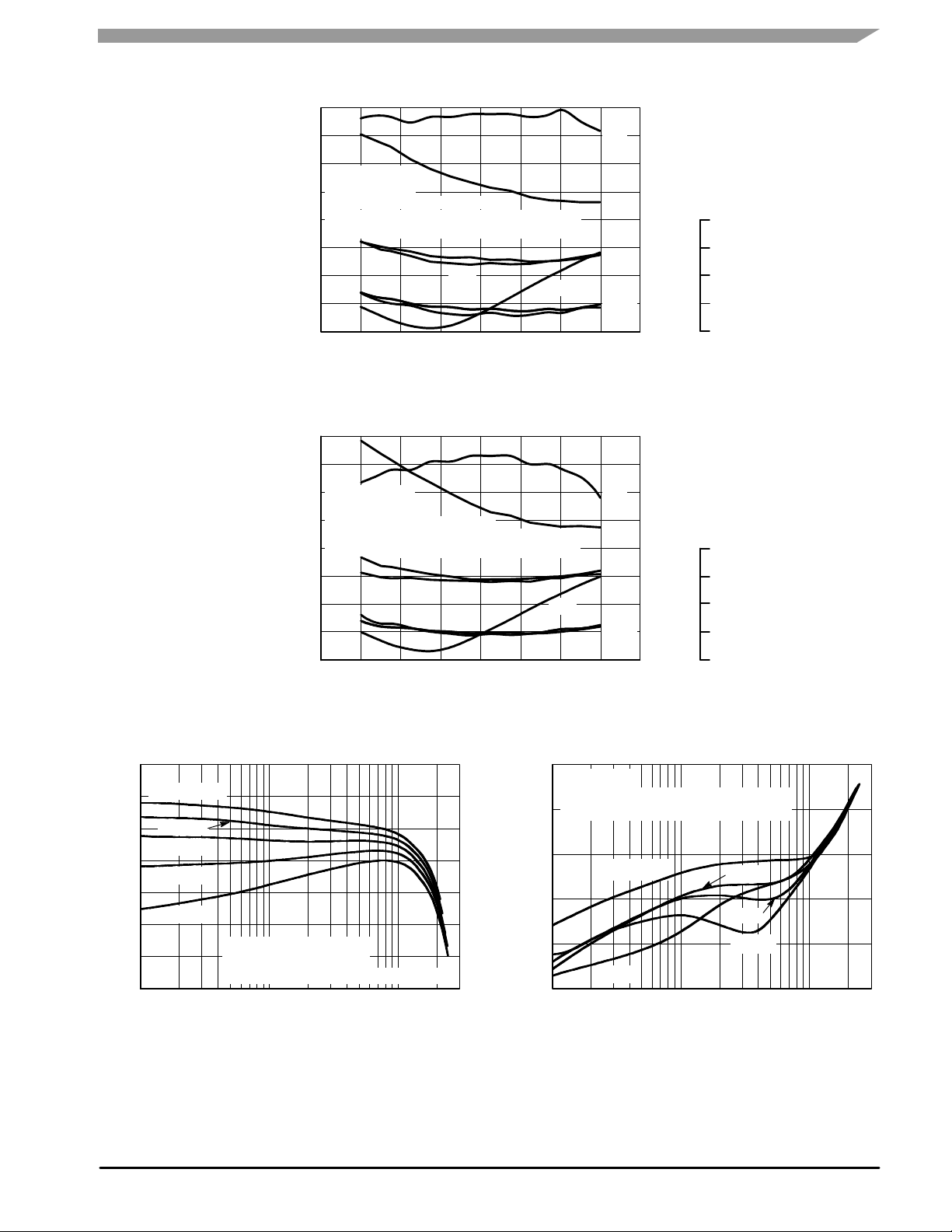
15.6
15.5
15.4
15.3
15.2
V
= 28 Vdc
DD
P
= 28 W (Avg.)
out
IDQ = 1300 mA, 2−Carrier W−CDMA
10 MHz Carrier Spacing, 3.84 MHz Channel Bandwidth
PAR = 8.5 dB @ 0.01% Probability (CCDF)
15.1
, POWER GAIN (dB)
ps
15
G
IM3
IRL
14.9
14.8
2410239023702350233023102290
f, FREQUENCY (MHz)
Figure 3. 2- Carrier W -CDMA Broadband Performance @ P
15.1
15
14.9
14.8
V
= 28 Vdc
DD
P
= 56 W (Avg.)
out
IDQ = 1300 mA, 2−Carrier W−CDMA
10 MHz Carrier Spacing, 3.84 MHz Channel Bandwidth
14.7
PAR = 8.5 dB @ 0.01% Probability (CCDF)
14.6
, POWER GAIN (dB)
ps
14.5
G
IM3
IRL
14.4
14.3
2410239023702350233023102290
f, FREQUENCY (MHz)
Figure 4. 2- Carrier W -CDMA Broadband Performance @ P
28
G
ps
27
26
25
η
D
−34
−36
−38
−40
ACPR
−42
24302270
= 28 Watts Avg.
out
38
37
36
G
ps
35
η
D
−25
−27
−29
ACPR
−31
−33
24302270
= 56 Watts Avg.
out
, DRAIN
D
η
EFFICIENCY (%)
−6
−9
−12
−15
IM3 (dBc), ACPR (dBc)
−18
IRL, INPUT RETURN LOSS (dB)
, DRAIN
D
η
EFFICIENCY (%)
−6
−9
−12
−15
IM3 (dBc), ACPR (dBc)
−18
IRL, INPUT RETURN LOSS (dB)
18
IDQ = 1950 mA
17
1625 mA
16
1300 mA
15
975 mA
14
, POWER GAIN (dB)
ps
13
G
12
650 mA
VDD = 28 Vdc
f1 = 2345 MHz, f2 = 2355 MHz
11
Two−Tone Measurements, 10 MHz Tone Spacing
1
P
, OUTPUT POWER (WATTS) PEP
out
Figure 5. Two- Tone Power Gain versus
RF Device Data
Freescale Semiconductor
10 300
100
Output Power
−10
VDD = 28 Vdc
f1 = 2345 MHz, f2 = 2355 MHz
−20
Two−Tone Measurements, 10 MHz Tone Spacing
−30
−40
IMD, THIRD ORDER
−50
INTERMODULATION DISTORTION (dBc)
−60
1
Figure 6. Third Order Intermodulation Distortion
IDQ = 650 mA
1950 mA
1625 mA
1300 mA
975 mA
10
P
, OUTPUT POWER (WATTS) PEP
out
versus Output Power
MRF6S23140HR3 MRF6S23140HSR3
100
300
5

TYPICAL CHARACTERISTICS
0
VDD = 28 Vdc, P
I
= 1300 mA, Two−Tone Measurements
DQ
−10
(f1 + f2)/2 = Center Frequency of 2350 MHz
−20
3rd Order
−30
5th Order
−40
= 140 W (PEP)
out
0.1
7th Order
1 100
10
−50
IMD, INTERMODULATION DISTORTION (dBc)
−60
TWO−TONE SPACING (MHz)
Figure 7. Intermodulation Distortion Products
versus Tone Spacing
59
57
55
P1dB = 52.22 dBm (162.72 W)
53
51
, OUTPUT POWER (dBm)
49
out
P
47
45
29
P6dB = 53.51 dBm (224.39 W)
P3dB = 53.04 dBm (201.42 W)
VDD = 28 Vdc, IDQ = 1300 mA
Pulsed CW, 8 µsec(on), 1 msec(off)
f = 2350 MHz
3331 3735 41
39
Pin, INPUT POWER (dBm)
Figure 8. Pulsed CW Output Power versus
Input Power
Ideal
Actual
43
42
36
30
, POWER GAIN (dB)
ps
24
18
12
6
0 −55
, DRAIN EFFICIENCY (%), G
D
0.5 300
η
Figure 9. 2 - Carrier W- CDMA ACPR, IM3, Power Gain
MRF6S23140HR3 MRF6S23140HSR3
6
V
= 28 Vdc, IDQ = 1300 mA
DD
−30_C
f1 = 2345 MHz, f2 = 2355 MHz
2−Carrier W−CDMA, 10 MHz
Carrier Spacing, 3.84 MHz Channel
Bandwidth, PAR = 8.5 dB @ 0.01%
Probability (CCDF)
η
TC = − 30_C
G
ps
D
85_C
−30_C
85_C
25_C
−30_C
25_C
IM3
ACPR
1 10 100
P
, OUTPUT POWER (WATTS) AVG.
out
and Drain Efficiency versus Output Power
25_C
85_C
−20
−25
−30
−35
−40
IM3 (dBc), ACPR (dBc)
−45
−50
RF Device Data
Freescale Semiconductor

TYPICAL CHARACTERISTICS
17
G
ps
16
15
TC = −30_C
25_C
85_C
14
VDD = 28 Vdc
, POWER GAIN (dB)
13
IDQ = 1300 mA
ps
G
f = 2350 MHz
12
η
D
11
0.5
1
P
, OUTPUT POWER (WATTS) CW
out
Figure 10. Power Gain and Drain Efficiency
versus Output Power
8
10
7
10
10010
−30_C
25_C
85_C
300
60
50
16
15
40
14
30
13
20
10
0
, POWER GAIN (dB)
ps
, DRAIN EFFICIENCY (%)
D
G
η
12
11
IDQ = 1300 mA
f = 2350 MHz
28 V
32 V
0 20050
VDD = 24 V
100 150
P
, OUTPUT POWER (WATTS) CW
out
Figure 11. Power Gain versus Output Power
250
6
MTTF (HOURS)
10
5
10
90
110 130 150 170 190
210 230
TJ, JUNCTION TEMPERATURE (°C)
This above graph displays calculated MTTF in hours when the device
is operated at VDD = 28 Vdc, P
= 28 W Avg., and ηD = 25%.
out
MTTF calculator available at http://www.freescale.com/rf. Select
Software & Tools/Development Tools/Calculators to access MTTF
calculators by product.
Figure 12. MTTF Factor versus Junction Temperature
250
RF Device Data
Freescale Semiconductor
MRF6S23140HR3 MRF6S23140HSR3
7

W- CDMA TEST SIGNAL
100
10
1
0.1
W−CDMA. ACPR Measured in 3.84 MHz Channel
Bandwidth @ ±5 MHz Offset. IM3 Measured in
0.01
PROBABILITY (%)
3.84 MHz Bandwidth @ ±10 MHz Offset. PAR =
8.5 dB @ 0.01% Probability on CCDF
0.001
0.0001
0
24 68
PEAK−TO−AVERAGE (dB)
Figure 13. CCDF W- CDMA 3GPP, Test Model 1,
64 DPCH, 67% Clipping, Single- Carrier Test Signal
+20
+30
0
−10
−20
(dB)
−30
−40
−50
−60
−IM3 in
3.84 MHz BW
−70
−80
10
3.84 MHz
Channel BW
−ACPR in
3.84 MHz BW
f, FREQUENCY (MHz)
+ACPR in
3.84 MHz BW
+IM3 in
3.84 MHz BW
20515100−5−10−15−20−25 25
Figure 14. 2-Carrier W-CDMA Spectrum
MRF6S23140HR3 MRF6S23140HSR3
8
RF Device Data
Freescale Semiconductor

Zo = 25 Ω
Z
source
f = 2300 MHz
f = 2400 MHz
f = 2300 MHz
Z
load
VDD = 28 Vdc, IDQ = 1300 mA, P
f
MHz
Z
source
W
out
2300 12.92 + j6.65 1.05 - j2.88
2310 13.06 + j6.73 1.04 - j2.82
2320 13.21 + j6.80 1.03 - j2.76
2330 13.37 + j6.87 1.01 - j2.70
2340 13.53 + j6.94 1.00 - j2.64
2350 13.70 + j7.01 0.99 - j2.58
2360 13.88 + j7.08 0.97 - j2.52
2370 14.06 + j7.14 0.96 - j2.46
2380 14.25 + j7.21 0.95 - j2.40
2390 14.45 + j7.27 0.94 - j2.34
2400 14.66 + j7.33 0.93 - j2.28
Z
= Test circuit impedance as measured from
source
gate to ground.
f = 2400 MHz
= 28 W Avg.
Z
load
W
RF Device Data
Freescale Semiconductor
Z
= Test circuit impedance as measured
load
Input
Matching
Network
from drain to ground.
Device
Under
Test
Z
source
Z
Output
Matching
Network
load
Figure 15. Series Equivalent Source and Load Impedance
MRF6S23140HR3 MRF6S23140HSR3
9

PACKAGE DIMENSIONS
B
B
(FLANGE)
K
4
G
1
2
D
M
bbb B
bbb B
ccc B
A
T
M
A
T
M
A
T
H
E
AA
(FLANGE)
Q2X
M
bbb B
3
M
M
(INSULATOR)
M
M
M
(LID)
N
M
M
C
SEATING
T
PLANE
M
A
T
M
ccc B
M
aaa B
M
NOTES:
1. DIMENSIONING AND TOLERANCING PER ANSI
Y14.5M−1994.
2. CONTROLLING DIMENSION: INCH.
3. DIMENSION H IS MEASURED 0.030 (0.762) AWAY
FROM PACKAGE BODY.
4. RECOMMENDED BOLT CENTER DIMENSION OF
1.16 (29.57) BASED ON M3 SCREW.
DIM MIN MAX MIN MAX
A 1.335 1.345 33.91 34.16
(LID)
R
M
S
M
M
(INSULATOR)
M
A
T
A
T
F
B 0.535 0.545 13.6 13.8
C 0.147 0.200 3.73 5.08
D 0.495 0.505 12.57 12.83
E 0.035 0.045 0.89 1.14
F 0.003 0.006 0.08 0.15
G 1.100 BSC 27.94 BSC
H 0.057 0.067 1.45 1.70
K 0.175 0.205 4.44 5.21
M 0.872 0.888 22.15 22.55
N 0.871 0.889 19.30 22.60
Q .118 .138 3.00 3.51
R 0.515 0.525 13.10 13.30
S 0.515 0.525 13.10 13.30
aaa 0.007 REF 0.178 REF
bbb 0.010 REF 0.254 REF
ccc 0.015 REF 0.381 REF
STYLE 1:
PIN 1. DRAIN
2. GATE
3. SOURCE
MILLIMETERSINCHES
CASE 465B- 03
ISSUE D
NI- 880
MRF6S23140HR3
B
B
(FLANGE)
K
M
bbb B
M
bbb B
T
M
ccc B
T
H
E
AA
(FLANGE)
NOTES:
1. DIMENSIONING AND TOLERANCING PER ANSI
1
2
D
M
M
M
M
(INSULATOR)
M
M
(LID)
N
M
R
M
ccc B
M
A
T
S
M
aaa B
M
A
T
(LID)
M
(INSULATOR)
M
A
T
A
A
C
Y14.5M−1994.
2. CONTROLLING DIMENSION: INCH.
3. DIMENSION H IS MEASURED 0.030 (0.762) AWAY
FROM PACKAGE BODY.
DIM MIN MAX MIN MAX
A 0.905 0.915 22.99 23.24
B 0.535 0.545 13.60 13.80
C 0.147 0.200 3.73 5.08
D 0.495 0.505 12.57 12.83
E 0.035 0.045 0.89 1.14
F 0.003 0.006 0.08 0.15
H 0.057 0.067 1.45 1.70
K 0.170 0.210 4.32 5.33
M 0.872 0.888 22.15 22.55
N 0.871 0.889 19.30 22.60
R 0.515 0.525 13.10 13.30
S 0.515 0.525 13.10 13.30
aaa 0.007 REF 0.178 REF
bbb 0.010 REF 0.254 REF
ccc 0.015 REF 0.381 REF
STYLE 1:
PIN 1. DRAIN
2. GATE
3. SOURCE
MILLIMETERSINCHES
F
SEATING
T
PLANE
CASE 465C- 02
ISSUE D
NI- 880S
MRF6S23140HSR3
MRF6S23140HR3 MRF6S23140HSR3
10
RF Device Data
Freescale Semiconductor

PRODUCT DOCUMENTATION
Refer to the following documents to aid your design process.
Application Notes
• AN1955: Thermal Measurement Methodology of RF Power Amplifiers
Engineering Bulletins
• EB212: Using Data Sheet Impedances for RF LDMOS Devices
REVISION HISTORY
The following table summarizes revisions to this document.
Revision Date Description
2 Dec. 2008 • Modified data sheet to reflect RF Test Reduction described in Product and Process Change Notification
number, PCN13232, p. 1, 2
• Removed Lower Thermal Resistance and Low Gold Plating bullets from Features section as functionality
is standard, p. 1
• Operating Junction Temperature increased from 200°C to 225°C in Maximum Ratings table and related
“Continuous use at maximum temperature will affect MTTF” footnote added, p. 1
• Corrected VDS to VDD in the RF test condition voltage callout for V
Functional Test”, On Characteristics table, p. 2
• Updated Part Numbers in Table 5, Component Designations and Values, to RoHS compliant part
numbers, p. 3
• Removed lower voltage tests from Fig. 11, Power Gain versus Output Power, due to fixed tuned fixture
limitations, p. 7
• Replaced Fig. 12, MTTF versus Junction Temperature with updated graph. Removed Amps2 and listed
operating characteristics and location of MTTF calculator for device, p. 7
• Added Product Documentation and Revision History, p. 11
, and added “Measured in
GS(Q)
RF Device Data
Freescale Semiconductor
MRF6S23140HR3 MRF6S23140HSR3
11

How to Reach Us:
Home Page:
www.freescale.com
Web Support:
http://www.freescale.com/support
USA/Europe or Locations Not Listed:
Freescale Semiconductor, Inc.
Technical Information Center, EL516
2100 East Elliot Road
Tempe, Arizona 85284
1-800 - 521 - 6274 or +1 - 480 - 768-2130
www.freescale.com/support
Europe, Middle East, and Africa:
Freescale Halbleiter Deutschland GmbH
Technical Information Center
Schatzbogen 7
81829 Muenchen, Germany
+44 1296 380 456 (English)
+46 8 52200080 (English)
+49 89 92103 559 (German)
+33 1 69 35 48 48 (French)
www.freescale.com/support
Japan:
Freescale Semiconductor Japan Ltd.
Headquarters
ARCO Tower 15F
1-8 - 1, Shimo - Meguro, Meguro - ku,
Tokyo 153 - 0064
Japan
0120 191014 or +81 3 5437 9125
support.japan@freescale.com
Asia/Pacific:
Freescale Semiconductor China Ltd.
Exchange Building 23F
No. 118 Jianguo Road
Chaoyang District
Beijing 100022
China
+86 10 5879 8000
support.asia@freescale.com
For Literature Requests Only:
Freescale Semiconductor Literature Distribution Center
P.O. Box 5405
Denver, Colorado 80217
1-800 - 441 - 2447 or +1 - 303 - 675-2140
Fax: +1-303 - 675 - 2150
LDCForFreescaleSemiconductor@hibbertgroup.com
Information in this document is provided solely to enable system and software
implementers to use Freescale Semiconductor products. There are no express or
implied copyright licenses granted hereunder to design or fabricate any integrated
circuits or integrated circuits based on the information in this document.
Freescale Semiconductor reserves the right to make changes without further notice to
any products herein. Freescale Semiconductor makes no warranty, representation or
guarantee regarding the suitability of its products for any particular purpose, nor does
Freescale Semiconductor assume any liability arising out of the application or use of
any product or circuit, and specifically disclaims any and all liability, including without
limitation consequential or incidental damages. “Typical” parameters that may be
provided in Freescale Semiconductor data sheets and/or specifications can and do
vary in different applications and actual performance may vary over time. All operating
parameters, including “Typicals”, must be validated for each customer application by
customer’s technical experts. Freescale Semiconductor does not convey any license
under its patent rights nor the rights of others. Freescale Semiconductor products are
not designed, intended, or authorized for use as components in systems intended for
surgical implant into the body, or other applications intended to support or sustain life,
or for any other application in which the failure of the Freescale Semiconductor product
could create a situation where personal injury or death may occur. Should Buyer
purchase or use Freescale Semiconductor products for any such unintended or
unauthorized application, Buyer shall indemnify and hold Freescale Semiconductor
and its officers, employees, subsidiaries, affiliates, and distributors harmless against all
claims, costs, damages, and expenses, and reasonable attorney fees arising out of,
directly or indirectly, any claim of personal injury or death associated with such
unintended or unauthorized use, even if such claim alleges that Freescale
Semiconductor was negligent regarding the design or manufacture of the part.
Freescalet and the Freescale logo are trademarks of Freescale Semiconductor, Inc.
All other product or service names are the property of their respective owners.
Freescale Semiconductor, Inc. 2006, 2008. All rights reserved.
MRF6S23140HR3 MRF6S23140HSR3
Document Number: MRF6S23140H
Rev. 2, 12/2008
12
RF Device Data
Freescale Semiconductor
 Loading...