


Freescale Semiconductor
Technical Data
RF Power Field Effect Transistors
N--Channel Enhancement--Mode Lateral MOSFETs
Designed for W--CDMA base station applications with frequencies from 2110
to 2170 MHz. Suitable for TDMA, CDMA and multicarrier amplifier applicati o ns . To be us ed in C l as s A B fo r P CN -- PCS / ce l lu l ar r a di o a nd W L L
applications.
• Typical 2--carrier W--CDMA Performance: VDD= 28 Volts, IDQ= 850 mA,
P
= 19 Watts Avg., f = 2112.5 MHz, Channel Bandwidth = 3.84 MHz,
out
PAR = 8.5 dB @ 0.01% Probability on CCDF.
Power Gain — 14.5 dB
Drain Efficiency — 26%
IM3 @ 10 MHz Offset — --37.5 dBc in 3.84 MHz Channel Bandwidth
ACPR @ 5 MHz Offset — --40.5 dBc in 3.84 MHz Channel Bandwidth
• Capable of Handling 10:1 VSWR, @ 28 Vdc, 2140 MHz, 90 Watts CW
Output Power
Features
• Characterized with Series Equivalent Large--Signal Impedance Parameters
• Internally Matched for Ease of Use
• Qualified Up to a Maximum of 32 VDDOperation
• Integrated ESD Protection
• Lower Thermal Resistance Package
• Low Gold Plating Thickness on Leads, 40
• RoHS Compliant
• In Tape and Reel. R3 Suffix = 250 Units per 56 mm, 13 inch Reel.
µ″ Nominal.
Document Number: MRF5S21090H
Rev. 3, 10/2008
MRF5S21090HR3
MRF5S21090HSR3
2110--2170 MHz, 19 W AVG., 28 V
2 x W -- CDMA
LATERAL N--CHANNEL
RF POWER MOSFETs
CASE 465 -- 06, STYLE 1
NI--780
MRF5S21090HR3
CASE 465A--06, STYLE 1
Table 1. Maximum Ratings
Rating Symbol Value Unit
Drain--Source Voltage V
LIFETIME BUY
Gate--Source Voltage V
Total Device Dissipation @ TC= 25°C
Derate above 25°C
Storage Temperature Range T
Case Operating Temperature T
Operating Junction Temperature T
Table 2. Thermal Characteristics
Characteristic Symbol Value
Thermal Resistance, Junction to Case
Case Temperature 80°C, 90 W CW
Case Temperature 76°C, 19 W CW
1. MTTF calculator available at http://www.freescale.com/rf. Select Software & Tools/Development Tools/Calculators to access MTTF
calculators by product.
2. Refer to AN1955, Thermal Measurement Methodology of RF Power Amplifiers. Go to http://www.freescale.com/rf.
Select Documentation/Application Notes -- AN1955.
R
DSS
GS
P
stg
θ
D
C
J
JC
NI--780S
MRF5S21090HSR3
--0.5, +65 Vdc
--0.5, +15 Vdc
269
1.5
--65 to +150 °C
150 °C
200 °C
(1,2)
0.65
0.69
W
W/°C
Unit
°C/W
LAST ORDER 3 OCT 08 LAST SHIP 14 MAY 09
Freescale Semiconductor, Inc., 2008. All rights reserved.
RF Device Data
Freescale Semiconductor
MRF5S21090HR3 MRF5S21090HSR3
1
Table 3. ESD Protection Characteristics
Test Conditions Class
Human Body Model 1 (Minimum)
Machine Model M3 (Minimum)
Charge Device Model C7 (Minimum)
Table 4. Electrical Characteristics
Characteristic Symbol Min Typ Max Unit
Off Characteristics
Zero Gate Voltage Drain Leakage Current
(VDS= 65 Vdc, VGS= 0 Vdc)
Zero Gate Voltage Drain Leakage Current
(VDS= 28 Vdc, VGS= 0 Vdc)
Gate--Source Leakage Current
(VGS= 5 Vdc, VDS= 0 Vdc)
On Characteristics (DC)
Gate Threshold Voltage
(VDS= 10 Vdc, ID= 200 µAdc)
Gate Quiescent Voltage
(VDS= 28 Vdc, ID= 850 mAdc)
Drain--Source On--Voltage
(VGS= 10 Vdc, ID= 2 Adc)
Forward Transconductance
(VDS= 10 Vdc, ID= 2 Adc)
Dynamic Characteristics
Reverse Transfer Capacitance
(VDS= 28 Vdc ± 30 mV(rms)ac @ 1 MHz, VGS= 0 Vdc)
Functional Tests (In Freescale Test Fixture, 50 ohm system) VDD= 28 Vdc, IDQ= 850 mA, P
2--carrier W--CDMA, 3.84 MHz Channel Bandwidth Carriers. ACPR measured in 3.84 MHz Channel Bandwidth @ ±5 MHz Offset. IM3
measured in 3.84 MHz Bandwidth @ ±10 MHz Offset. PAR = 8.5 dB @ 0.01% Probability on CCDF.
Power Gain G
Drain Efficiency η
Intermodulation Distortion IM3 — --37.5 --35 dBc
Adjacent Channel Power Ratio ACPR — --40.5 --38 dBc
LIFETIME BUY
Input Return Loss IRL — --15 --9 dB
1. Part is internally matched both on input and output.
(1)
(TC= 25°C unless otherwise noted)
I
I
I
V
GS(th)
V
GS(Q)
V
DS(on)
C
DSS
DSS
GSS
g
fs
rss
ps
D
— — 10 µAdc
— — 1 µAdc
— — 1 µAdc
2.5 2.9 3.5 Vdc
— 3.9 — Vdc
— 0.25 — Vdc
— 5 — S
— 1.7 — pF
= 19 W Avg., f = 2112.5 MHz,
out
12.5 14.5 — dB
24 26 — %
MRF5S21090HR3 MRF5S21090HSR3
2
LAST ORDER 3 OCT 08 LAST SHIP 14 MAY 09
RF Device Data
Freescale Semiconductor
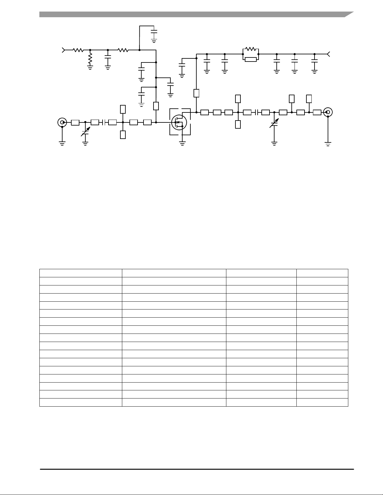
V
BIAS
R1
R2
C4
R3
C5
C3
C10
R4
W1
V
SUPPLY
+
C12C11
C13C8C7
RF
INPUT
C6
Z4
Z1 Z2 Z3 Z6 Z7
C1
C14
Z5
Z1 1.0856″ x 0.080″ Microstrip
Z2 0.130″ x 0.080″ Microstrip
Z3 0.230″ x 0.080″ Microstrip
Z4 0.347″ x 0.208″ Microstrip
Z5 0.090″ x 0.208″ Microstrip
Z6 0.650″ x 0.176″ Taper
Z7 0.623″ x 0.610″ Microstrip
Z8 0.044″ x 0.881″ Microstrip
Z9 0.044″ x 0.869″ Microstrip
Z10 1.076″ x 0.446″ Microstrip
Z11 0.320″ x 0.393″ Microstrip
C9
Z9
DUT
Z8
Z11 Z12 Z16 Z17 Z19 Z21
Z10
Z12 0.609″ x 0.220″ Microstrip
Z13 0.290″ x 0.106″ Microstrip
Z14 0.290″ x 0.106″ Microstrip
Z15 0.080″ x 0.025″ Microstrip
Z16 1.080″ x 0.160″ Microstrip
Z17 0.180″ x 0.080″ Microstrip
Z18 0.260″ x 0.147″ Microstrip
Z19 0.500″ x 0.080″ Microstrip
Z20 0.199″ x 0.147″ Microstrip
Z21 0.365″ x 0.080″ Microstrip
PCB Arlon GX0300--55--22, 0.03″, εr= 2.55
Z13
Z14
Z15
C2
Z18 Z20
C15
Figure 1. MRF5S21090HR3(HSR3) Test Circuit Schematic
Table 5. MRF5S21090HR3(HSR3) Test Circuit Component Designations and Values
Part Description Part Number Manufacturer
C1 9.1 pF Chip Capacitor ATC100B9R1CT500XT ATC
C2 8.2 pF Chip Capacitor ATC100B8R2CT500XT ATC
C3 2.0 pF Chip Capacitor ATC100B2R0BT500XT ATC
C4, C12 0.1 µF Chip Capacitors CDR33BX104AKYS Kemet
LIFETIME BUY
C5 5.6 pF Chip Capacitor ATC100B5R6CT500XT ATC
C6 5.1 pF Chip Capacitor ATC100B5R1CT500XT ATC
C7 7.5 pF Chip Capacitor ATC100B7R5JT500XT ATC
C8 1.2 pF Chip Capacitor ATC100B1R2BT500XT ATC
C9, C10 0.56 µF Chip Capacitors 700A561MT150XT ATC
C11 1000 pF Chip Capacitor ATC100B102JT500XT ATC
C13 470 µF, 35 V Electrolytic Capacitor EKME630ELL471MK25S Nippon Chemi--Con
C14, C15 0.4 – 2.5 Variable Capacitors, Gigatrim 27281SL Johanson
R1
R2
R3, R4
W1 Wire Strap
1 kΩ, 1/4 W Chip Resistor
560 kΩ, 1/4 W Chip Resistor
12 Ω, 1/4 W Chip Resistors
CRCW12061001FKEA Vishay
CRCW12065600FKEA Vishay
CRCW120612R0FKEA Vishay
RF
OUTPUT
RF Device Data
Freescale Semiconductor
LAST ORDER 3 OCT 08 LAST SHIP 14 MAY 09
MRF5S21090HR3 MRF5S21090HSR3
3

W1
C13
V
DD
C3C4C5
C10
R2
R1
R3
V
GG
C9
C6
C7 C8
C11
R4
C12
C1
C14
CUT OUT AREA
Frees cale has b egu n th e tra nsit ion of ma rki ng Pr int e d Circu it Bo ard s (PC Bs) with the Free scal e Se mico ndu ctor
signature/logo. PCBs may have either Motorola or Freescale markings during the transition period. These changes will have
no impact on form, fit or function of the current product.
Figure 2. MRF5S21090HR3(HSR3) Test Circuit Component Layout
C2
C15
MRF5S21090
Rev 5
LIFETIME BUY
MRF5S21090HR3 MRF5S21090HSR3
4
LAST ORDER 3 OCT 08 LAST SHIP 14 MAY 09
RF Device Data
Freescale Semiconductor

TYPICAL CHARACTERISTICS
15
G
ps
14
13
η
12
IRL
11
10
9
, POWER GAIN (dB)
8
ps
IM3
G
7
6
ACPR
5
VDD= 28 Vdc, P
2--Carrier W--CDMA, 10 MHz Carrier Spacing
D
3.84 MHz Channel Bandwidth, PAR = 8.5 dB
@ 0.01% Probability (CCDF)
f, FREQUENCY (MHz)
= 19 W (Avg.), IDQ= 850 mA
out
40
35
30
, DRAIN
D
25
η
20
--20
--25
--30
--35
--40
--45
2200218021602140212021002080
EFFICIENCY (%)
--10
--15
--20
--25
--30
IM3 (dBc), ACPR (dBc)
INPUT RETURN LOSS (dB)IRL,
--35
Figure 3. 2--Carrier W-- CDMA Broadband Performance
17
VDD= 28 Vdc f1 = 2135 MHz, f2 = 2145 MHz
IDQ= 1200 mA
16
1000 mA
15
850 mA
14
650 mA
, POWER GAIN (dB)
ps
G
13
450 mA
12
Two--Tone Measurement, 10 MHz Tone Spacing
1
P
, OUTPUT POWER (WATTS) PEP
out
10
100
Figure 4. Two--Tone Power Gain versus
Output Power
--15
VDD= 28 Vdc
f1 = 2135 MHz, f2 = 2145 MHz
--20
Two--Tone Measurement, 10 MHz Tone Spacing
--25
--30
--35
IMD,THIRD ORDER
--40
--45
INTERMODULATION DISTORTION (dBc)
--50
650 mA
1
P
IDQ= 450 mA
1200 mA
10
, OUTPUT POWER (WATTS) PEP
out
1000 mA
850 mA
100
Figure 5. 3rd Order Intermodulation Distortion
versus Output Power
LIFETIME BUY
--20
--25
3rd Order
--30
--35
5th Order
--40
--45
7th Order
--50
INTERMODULATION DISTORTION (dBc)IMD,
--55
--60
0.1
Figure 6. Intermodulation Distortion Products
RF Device Data
Freescale Semiconductor
VDD= 28 Vdc, P
Two--Tone Measurements
(f1 + f2)/2 = Center Frequency of 2140 MHz
1
TWO--TONE SPACING (MHz)
= 90 W (PEP), IDQ= 850 mA
out
versus Tone Spacing
57
55
53
P1dB = 50.47 dBm (111.4 W)
51
49
, OUTPUT POWER (dBm)
out
P
47
45
10
30
P3dB = 51.17 dBm (130.9 W)
VDD= 28 Vdc, IDQ= 850 mA
Pulsed CW, 8 µsec(on), 1 msec(off)
f = 2140 MHz
32 34 36 38 40
Pin, INPUT POWER (dBm)
Figure 7. Pulse CW Output Power versus
Ideal
Actual
42
LAST ORDER 3 OCT 08 LAST SHIP 14 MAY 09
Input Power
MRF5S21090HR3 MRF5S21090HSR3
5

TYPICAL CHARACTERISTICS
--1
5
4
0
η
,
D
R
A
I
N
E
F
F
I
C
I
E
N
C
Y
(
%
)
,
G
,
P
O
W
E
R
G
A
I
N
(
d
B
)
1
0
9
.
0
VDD= 28 Vdc, IDQ= 850 mA, f1 = 2135 MHz,
35
f2 = 2145 MHz, 2 x W--CDMA, 10 MHz
@ 3.84 MHz Bandwidth, PAR = 8.5 dB
30
@ 0.01% Probability (CCDF)
25
ps
20
15
10
D
G
ps
IM3
5
0 --55
1 10
P
, POWER (WATTS) W--CDMA
out
η
D
ACPR
Figure 8. 2--Carrier W-- CDMA ACPR, IM3,
Power Gain and Drain Efficiency
versus Output Power
W--CDMA TEST SIGNAL
--20
--25
--30
--35
--40
--45
--50
)
2
8
10
7
10
IM3 (dBc), ACPR (dBc)
MTTF FACTOR (HOURS x AMPS
6
10
100
120 140 160 180 200
TJ, JUNCTION TEMPERATURE (°C)
This above graph displays calculated MTTF in hours x ampere
drain current. Life tests at elevated temperatures have correlated to
better than ±10% of the theoretical prediction for metal failure. Divide
MTTF factor by I
2
for MTTF in a particular application.
D
Figure 9. MTTF Factor versus Junction Temperature
220
2
100
10
1
0.1
0.01
W--CDMA. ACPR Measured in 3.84 MHz Channel
Bandwidth @ ±5 MHz Offset. IM3 Measured in
LIFETIME BUY
.001
3.84 MHz Bandwidth @ ±10 MHz Offset. PAR =
8.5 dB @ 0.01% Probability on CCDF
0001
0
2 4 6 8
PEAK--TO--AVERAGE (dB)
Figure 10. CCDF W--CDMA 3GPP, Test Model 1,
64 DPCH, 67% Clipping, Single Carrier Test Signal
--20
--30
--40
--50
--60
--70
(dB)
--80
--90
--100
--IM3 in
3.84 MHz BW
--110
--120
10
3.84 MHz
Channel BW
--ACPR in
3.84 MHz BW
f, FREQUENCY (MHz)
+ACPR in
3.84 MHz BW
+IM3 in
3.84 MHz BW
205 15100--5--10--15--20--25 25
Figure 11. 2-Carrier W-CDMA Spectrum
LAST ORDER 3 OCT 08 LAST SHIP 14 MAY 09
MRF5S21090HR3 MRF5S21090HSR3
RF Device Data
6
Freescale Semiconductor

f = 2200 MHz
Z
load
f = 2200 MHz
f = 2100 MHz
Z
source
Zo= 10 Ω
f = 2100 MHz
LIFETIME BUY
VDD= 28 Vdc, IDQ= 850 mA, P
f
MHz
2100
2120
2160
2200 1.8 -- j1.63.0 -- j4.0
Z
= Test circuit impedance as measured from
source
Z
= Test circuit impedance as measured
load
Input
Matching
Network
Z
source
Ω
3.4 -- j5.1
3.2 -- j5.4
3.0 -- j4.4
gate to ground.
from drain to ground.
Device
Under
Test
Z
source
out
Z
= 19 W Avg.
Z
load
Ω
2.4 -- j2.0
2.2 -- j2.1
2.1 -- j1.9
load
Output
Matching
Network
LAST ORDER 3 OCT 08 LAST SHIP 14 MAY 09
RF Device Data
Freescale Semiconductor
Figure 12. Series Equivalent Source and Load Impedance
MRF5S21090HR3 MRF5S21090HSR3
7

PACKAGE DIMENSIONS
B
B
(FLANGE)
bbb B
H
E
A A
G
D
M
T
(FLANGE)
Q
1
2
M
A
2X
3
K
M
(INSULATOR)
M
M
bbb B
T
(LID)
N
M
ccc B
T
M
bbb B
M
A
M
A
M
A
T
M
M
M
M
ccc B
aaa B
A
T
M
A
T
(LID)
R
M
(INSULATOR)
S
M
M
M
C
SEATING
T
PLANE
NOTES:
1. DIMENSIONING AND TOLERANCING PER ANSI
Y14.5M--1994.
2. CONTROLLING DIMENSION: INCH.
3. DELETED
4. DIMENSION H IS MEASURED 0.030 (0.762) AWAY
FROM PACKAGE BODY.
DIM MIN MAX MIN MAX
A 1.335 1.345 33.91 34.16
B 0.380 0.390 9.65 9.91
C 0.125 0.170 3.18 4.32
D 0.495 0.505 12.57 12.83
E 0.035 0.045 0.89 1.14
F 0.003 0.006 0.08 0.15
G 1.100 BSC 27.94 BSC
H 0.057 0.067 1.45 1.70
K 0.170 0.210 4.32 5.33
M 0.774 0.786 19.66 19.96
N 0.772 0.788 19.60 20.00
Q .118 .138 3.00 3.51
R 0.365 0.375 9.27 9.53
S 0.365 0.375 9.27 9.52
aaa 0.005 REF 0.127 REF
bbb 0.010 REF 0.254 REF
ccc 0.015 REF 0.381 REF
F
STYLE 1:
PIN 1. DRAIN
2. GATE
3. SOURCE
MILLIMETERSINCHES
CASE 465--06
ISSUE G
NI--780
MRF5S21090HR3
U
4X
(FLANGE)
B
B
(FLANGE)
H
A
M
bbb B
E
(FLANGE)
NOTES:
Z
4X
1
2X
2
(LID)
K
D
M
A
T
M
(LID)
N
M
ccc B
(INSULATOR)
M
M
bbb B
C
3
(LID)
M
A
T
A
T
M
M
M
M
ccc B
M
aaa B
R
M
(INSULATOR)
S
M
M
M
A
T
A
T
F
SEATING
T
A
PLANE
1. DIMENSIONING AND TOLERANCING PER ANSI
Y14.5M--1994.
2. CONTROLLING DIMENSION: INCH.
3. DELETED
4. DIMENSION H IS MEASURED 0.030 (0.762) AWAY
FROM PACKAGE BODY.
DIM MIN MAX MIN MAX
A 0.805 0.815 20.45 20.70
B 0.380 0.390 9.65 9.91
C 0.125 0.170 3.18 4.32
D 0.495 0.505 12.57 12.83
E 0.035 0.045 0.89 1.14
F 0.003 0.006 0.08 0.15
H 0.057 0.067 1.45 1.70
K 0.170 0.210 4.32 5.33
M 0.774 0.786 19.61 20.02
N 0.772 0.788 19.61 20.02
R 0.365 0.375 9.27 9.53
S 0.365 0.375 9.27 9.52
U ------ 0.040 ------ 1.02
Z ------ 0.030 ------ 0.76
aaa 0.005 REF 0.127 REF
bbb 0.010 REF 0.254 REF
ccc 0.015 REF 0.381 REF
STYLE 1:
PIN 1. DRAIN
2. GATE
5. SOURCE
MILLIMETERSINCHES
CASE 465A--06
ISSUE H
NI--780S
MRF5S21090HSR3
MRF5S21090HR3 MRF5S21090HSR3
8
RF Device Data
Freescale Semiconductor

PRODUCT DOCUMENTATION
Refer to the following documents to aid your design process.
Application Notes
• AN1955: Thermal Measurement Methodology of RF Power Amplifiers
Engineering Bulletins
• EB212: Using Data Sheet Impedances for RF LDMOS Devices
REVISION HISTORY
The following table summarizes revisions to this document.
Revision Date Description
3 Oct. 2008 • Modified data sheet to reflect RF Test Reduction described in Product and Process Change Notification
number, PCN12779, p. 1, 2
• Updated Part Numbers in Table 5, Component Designations and Values, to RoHS compliant part
numbers, p. 3
• Added Product Documentation and Revision History, p. 9
RF Device Data
Freescale Semiconductor
MRF5S21090HR3 MRF5S21090HSR3
9

How to Reach Us:
Home Page:
www.freescale.com
Web Support:
http://www.freescale.com/support
USA/Europe or Locations Not Listed:
Freescale Semiconductor, Inc.
Technical Information Center, EL516
2100 East Elliot Road
Tempe, Arizona 85284
1--800--521--6274 or +1--480--768--2130
www.freescale.com/support
Europe, Middle East, and Africa:
Freescale Halbleiter Deutschland GmbH
Technical Information Center
Schatzbogen 7
81829 Muenchen, Germany
+44 1296 380 456 (English)
+46 8 52200080 (English)
+49 89 92103 559 (German)
+33 1 69 35 48 48 (French)
www.freescale.com/support
Japan:
Freescale Semiconductor Japan Ltd.
Headquarters
ARCO Tower 15F
1--8-- 1, Shimo--Meguro, Meguro--ku,
Tokyo 153--0064
Japan
0120 191014 or +81 3 5437 9125
support.japan@freescale.com
Asia/Pacific:
Freescale Semiconductor China Ltd.
Exchange Building 23F
No. 118 Jianguo Road
Chaoyang District
Beijing 100022
China
+86 10 5879 8000
support.asia@freescale.com
For Literature Requests Only:
Freescale Semiconductor Literature Distribution Center
P.O. Box 5405
Denver, Colorado 80217
1--800--441--2447 or +1--303--675--2140
Fax: +1--303--675--2150
LDCForFreescaleSemiconductor@hibbertgroup.com
Information in this document is provided solely to enable system and software
implementers to use Freescale Semiconductor products. There are no express or
implied copyright licenses granted hereunder to design or fabricate any integrated
circuits or integrated circuits based on the information in this document.
Freescale Semiconductor reserves the right to make changes without further notice to
any products herein. Freescale Semiconductor makes no warranty, representation or
guarantee regarding the suitability of its products for any particular purpose, nor does
Freescale Semiconductor assume any liability arising out of the application or use of
any product or circuit, and specifically disclaims any and all liability, including without
limitation consequential or incidental damages. “Typical” parameters that may be
provided in Freescale Semiconductor data sheets and/or specifications can and do
vary in different applications and actual performance may vary over time. All operating
parameters, including “Typicals”, must be validated for each customer application by
customer’s technical experts. Freescale Semiconductor does not convey any license
under its patent rights nor the rights of others. Freescale Semiconductor products are
not designed, intended, or authorized for use as components in systems intended for
surgical implant into the body, or other applications intended to support or sustain life,
or for any other application in which the failure of the Freescale Semiconductor product
could create a situation where personal injury or death may occur. Should Buyer
purchase or use Freescale Semiconductor products for any such unintended or
unauthorized application, Buyer shall indemnify and hold Freescale Semiconductor
and its officers, employees, subsidiaries, affiliates, and distributors harmless against all
claims, costs, damages, and expenses, and reasonable attorney fees arising out of,
directly or indirectly, any claim of personal injury or death associated with such
unintended or unauthorized use, even if such claim alleges that Freescale
Semiconductor was negligent regarding the design or manufacture of the part.
Freescalet and the Freescale logo are trademarks of Freescale Semiconductor, Inc.
All other product or service names are the property of their respective owners.
Freescale Semiconductor, Inc. 2008. All rights reserved.
MRF5S21090HR3 MRF5S21090HSR3
Document Number: MRF5S21090H
Rev. 3, 10/2008
10
RF Device Data
Freescale Semiconductor
 Loading...