

Page 1
C
O
O
Freescale Semiconductor
Technical Data
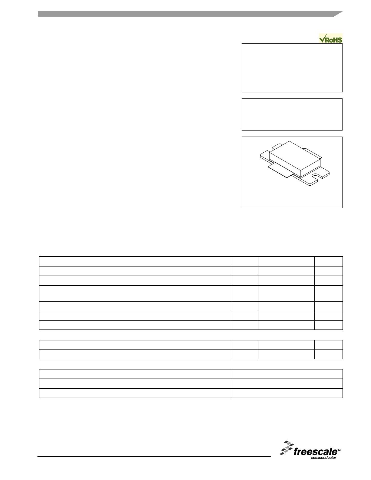
RF Power Field Effect Transistor
N--Channel Enhancement--Mode Lateral MOSFET
Designed for GSM and GSM EDGE base station applications withfrequencies
from 1800 to 2000 MHz. Suitable for FM, TDMA, CDMA and multicarrier amplifier
applications. To be used in C lass AB for GSM and GSM EDGE cellular radio
applications.
! GSM and GSM EDGE Performances @ 1805 MHz
Power Gain — 13.5 dB (Typ) @ 90 Watts CW
Efficiency — 52% (Typ) @ 90 Watts CW
! Capable of Handling 10:1 VSWR, @ 26 Vdc, 90 Watts CW Output Power
Features
! Internally Matched for Ease of Use
! High Gain, High Efficiency and High Linearity
N
! Integrated ESD Protection
! Designed for Maximum Gain and Insertion Phase Flatness
! Excellent Thermal Stability
! Characterized with Series Equivalent Large--Signal Impedance Parameters
! RoHS Compliant
! In Tape and Reel. R3 Suffix = 250 Units per 56 mm, 13 inch Reel.
Document Number: MRF18090A
Rev . 8, 10/2008
MRF18090AR3
1805-- 1880 MHz, 90 W, 26 V
LATERAL N--CHANNEL
RF POWER MOSFET
CASE 465B--03, STYLE 1
NI--880
RMATI
Table 1. Maximum Ratings
Rating Symbol Value Unit
Drain--Source Voltage V
Gate--Source Voltage V
Total Device Dissipation @ TC=25"C
Derate above 25"C
HIVE INF
Storage Temperature Range T
Case Operating Temperature T
Operating Junction Temperature T
AR
Table 2. Thermal Characteristics
Characteristic Symbol Value Unit
Thermal Resistance, Junction to Case R
Table 3. ESD Protection Characteristics
Test Conditions Class
Human Body Model 2 (Minimum)
Machine Model M3 (Minimum)
DSS
GS
P
stg
#
D
C
J
JC
--0.5, +65 Vdc
--0.5, +15 Vdc
-- 65 to +150 "C
250
1.43
150 "C
200 "C
0.7 "C/W
W
W/"C
RCHIVE INFORMATION
$ Freescale Semiconductor, Inc., 2008, 2010.All rights reserved.
RF Device Data
Freescale Semiconductor
MRF18090AR3
1
Page 2
C
O
O
Table 4. Electrical Characteristics
Characteristic
Off Characteristics
Drain--Source Breakdown Voltage
(V
=0Vdc,ID= 100 %Adc)
GS
Zero Gate Voltage Drain Current
(V
=26Vdc,VGS=0Vdc)
DS
Gate--Source Leakage Current
(V
=5Vdc,VDS=0Vdc)
GS
On Characteristics
Gate Quiescent Voltage
(V
=26Vdc,ID= 750 mAdc)
DS
Drain--Source On--Voltage
(V
=10Vdc,ID=1Adc)
GS
N
Forward Transconductance
(V
=10Vdc,ID=3Adc)
DS
Dynamic Characteristics
Reverse Transfer Capacitance
(V
=26Vdc& 30 mV(rms)ac @ 1 MHz, VGS=0Vdc)
DS
Functional Tests (In Freescale Test Fixture)
Common--Source Amplifier Power Gain @ 90 W
(V
=26Vdc,IDQ= 750 mA, f = 1805 MHz)
DD
RMATI
Drain Efficiency @ 90 W
(V
=26Vdc,IDQ= 750 mA, f = 1805 MHz)
DD
Input Return Loss
(V
=26Vdc,P
DD
=90WCW,IDQ= 750 mA, f = 1805 MHz)
out
(TC=25"C unless otherwise noted)
Symbol Min Typ Max Unit
V
(BR)DSS
I
DSS
I
GSS
V
GS(Q)
V
DS(on)
g
fs
C
rss
G
ps
' 47 52 — %
IRL — — -- 1 0 dB
65 — — Vdc
— — 10 %Adc
— — 1 %Adc
2.5 3.7 4.5 Vdc
— 0.1 — Vdc
— 7.2 — S
— 4.2 — pF
12.0 13.5 — dB
HIVE INF
AR
MRF18090AR3
2
RCHIVE INFORMATION
RF Device Data
Freescale Semiconductor
Page 3
C
O
O
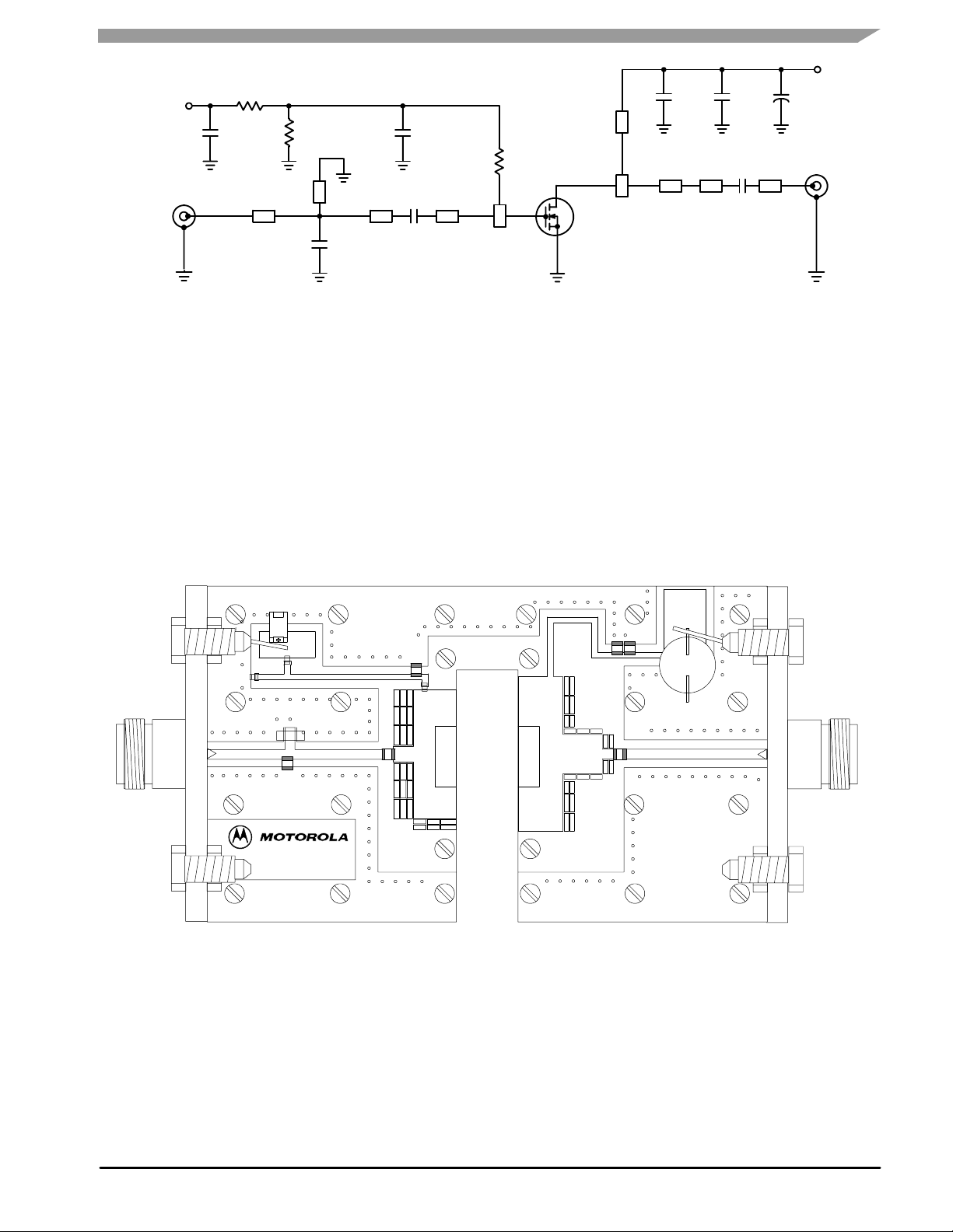
V
V
BIAS
INPUT
RF
R1
+
C1
R2
Z1
Z2
C2
R3
Z3
Z4
Z5
Z10
Z6
C5
Z7 Z8
C6
C7
+
Z9
SUPPLY
C8
RF
OUTPUT
N
RMATI
V
C4
C1 10 mF, 35 V Tantalum Capacitor
C2, C3 10 pF, 100B Chip Capacitors
C4 3.3 pF, 100B Chip Capacitor
C5, C6 6.8 pF, 100B Chip Capacitors
C7 12 pF, 100B Chip Capacitor
C8 220 mF, 63 V Electrolytic Capacitor
R1, R2 10 kΩ, 1/8 W Chip Resistors (0805)
R3 1.0 kΩ, 1/8 W Chip Resistor (0805)
Z1 0.697( x 0.087( Microstrip
Z2 0.087( x 0.197( Microstrip
Figure 1. MRF18090A 1805 -- 1880 MHz Test Fixture Schematic
C1
BIAS
R2
R1
C3
C2
R3
DUT
Z3 0.819( x 0.087( Microstrip
Z4 0.181( x 0.144( Microstrip
Z5 0.383( x 1.148( Microstrip
Z6 0.400( x 1.380( Microstrip
Z7 0.351( x 0.351( Microstrip
Z8 0.126( x 0.087( Microstrip
Z9 1.280( x 0.087( Microstrip
Z10 )1.275( x 0.055( Microstrip
PCB Taconic TLX8--0300, 0.030(, *
C6
C5
C8
=2.55
r
V
SUPPLY
HIVE INF
C4
AR
Ground
(bias)
Freescale has begun the transition of marking Printed Circuit Boards (PCBs) with the Freescale Semiconductor signature/logo. PCBs may have either Motorola or Freescale markings during the transition period.
These changes will have no impact on form, fit or function of the current product.
RF Device Data
Freescale Semiconductor
MRF18090A
Rev 4
Figure 2. MRF18090A 1805 -- 1880 MHz Test Fixture Component Layout
C3
CUT OUT AREA
C7
Ground
(supply)
MRF18090AR3
RCHIVE INFORMATION
3
Page 4

C
O
O
T1
C1
T1
R1
R2
R6
C2
R5
C5
V
+
SUPPLY
N
RMATI
R3
R4
C3
T2
C4
RF
INPUT
C1, C3 1 mF Chip Capacitors (0805)
C2 0.1 mF Chip Capacitor (0805)
C4 1 nF Chip Capacitor (0805)
C5 220 mF, 50 V Electrolytic Capacitor
C6, C7 8.2 pF, 100A Chip Capacitors
C8, C9, C10 22 pF, 100A Chip Capacitors
R1 10 + Chip Resistor (0805)
R2, R3 1 k+ Chip Resistors (0805)
R4 2.2 k+ Chip Resistor (0805)
Figure 3. 1805 -- 1880 MHz Demo Board Schematic
Z1
C8
Z2
C6
C7
C9
Z3
C10
R5 10 k+ Chip Resistor (0603)
R6 5 k+, SMD Potentiometer
T1 LP2951 Micro--8 Voltage Regulator
T2 BC847 SOT--23 NPN Transistor
Z1 0.210( x 0.055( Microstrip
Z2 0.419( x 0.787( Microstrip
Z3 0.836( x 0.512( Microstrip
Z4 0.164( x 0.055( Microstrip
Substrate = 0.5 mm Teflon
,
Glass
RF
OUTPUT
Z4
HIVE INF
AR
V Ground
SUPPLY
R6
T1
C4
C2
R5
C3
MRF18090A
C5
C6
C7
MRF18090A
C9
C10
C1R2R1
R3
Freescale has begun the transition of marking Printed Circuit Boards (PCBs) with the Freescale
Semiconductor signature/logo. PCBs may have either Motorola or Freescale markings during the
transition period. These changes will have no impact on form, fit or function of the current product.
Figure 4. 1805 -- 1880 MHz Demo Board Component Layout
R4
T2
C8
RCHIVE INFORMATION
MRF18090AR3
4
RF Device Data
Freescale Semiconductor
Page 5

C
O
O
TYPICAL CHARACTERISTICS
N
RMATI
16
IDQ= 1000 mA
750 mA
500 mA
300 mA
VDD=26Vdc
f = 1880 MHz
1.0 18 321614
P
, OUTPUT POWER (WATTS)
out
Figure 5. Power Gain versus
Output Power
Pin=3.65W
2W
1W
0
1.795 0
1.835 345
f, FREQUENCY (GHz)
10
VDD=26Vdc
I
= 750 mA
DQ
1.855 1.875
100 3022
1.895
, POWER GAIN (dB)
ps
G
100
out
P , OUTPUT POWER (WATTS)
15
14
13
12
11
10
90
80
70
60
50
40
30
20
10
120
100
out
P , OUTPUT POWER (WATTS)
120
IDQ= 750 mA
100
f = 1880 MHz
80
60
40
, OUTPUT POWER (WATTS)
out
P
20
0
120.1
V
DD
Figure 6. Output Power versus Supply Voltage
η
80
60
40
20
0
1
Pin, INPUT POWER (WATTS)
Pin=3.65W
2W
1W
, SUPPLY VOLTAGE (VOLTS)
P
out
VDD=26Vdc
I
= 750 mA
DQ
f = 1880 MHz
21.815
2820 24
26
60
50
40
30
20
, DRAIN EFFICIENCY (%)'
10
0
Figure 7. Output Power versus Frequency
HIVE INF
AR
RF Device Data
Freescale Semiconductor
Figure 8. Output Power and Efficiency
versus Input Power
15
G
ps
12
, POWER GAIN (dB)
9
ps
G
6
1.75
VDD=26Vdc
I
= 750 mA
DQ
f, FREQUENCY (GHz)
Figure 9. Wideband Gain and IRL
(at Small Signal)
IRL
0
-- 5
-- 1 0
-- 1 5
-- 2 0
IRL, INPUT RETURN LOSS (dB)
-- 2 5
-- 3 0
1.951.851.80 1.90
MRF18090AR3
5
RCHIVE INFORMATION
Page 6

C
O
O
N
f = 1805 MHz
f = 1990 MHz
Z
load
Zo=10+
f = 1990 MHz
RMATI
HIVE INF
AR
f = 1805 MHz
VDD=26V,IDQ= 750 mA, P
f
MHz
1805
1880
1930
1990 2.30 -- j7.30 0.82 -- j2.90
Z
= Test circuit impedance as measured from
source
Z
load
Input
Matching
Network
gate to ground.
= Test circuit impedance as measured
from drain to ground.
Z
source
Z
source
+
1.10 -- j5.85
1.56 -- j6.75
2.05 -- j8.00
Device
Under T est
= 90 Watts (CW)
out
1.15 -- j2.16
1.13 -- j2.60
1.30 -- j2.23
Z
load
+
RCHIVE INFORMATION
Output
Matching
Network
MRF18090AR3
6
Z
source
Figure 10. Large Signal Source and Load Impedance
Z
load
RF Device Data
Freescale Semiconductor
Page 7
C
O
O
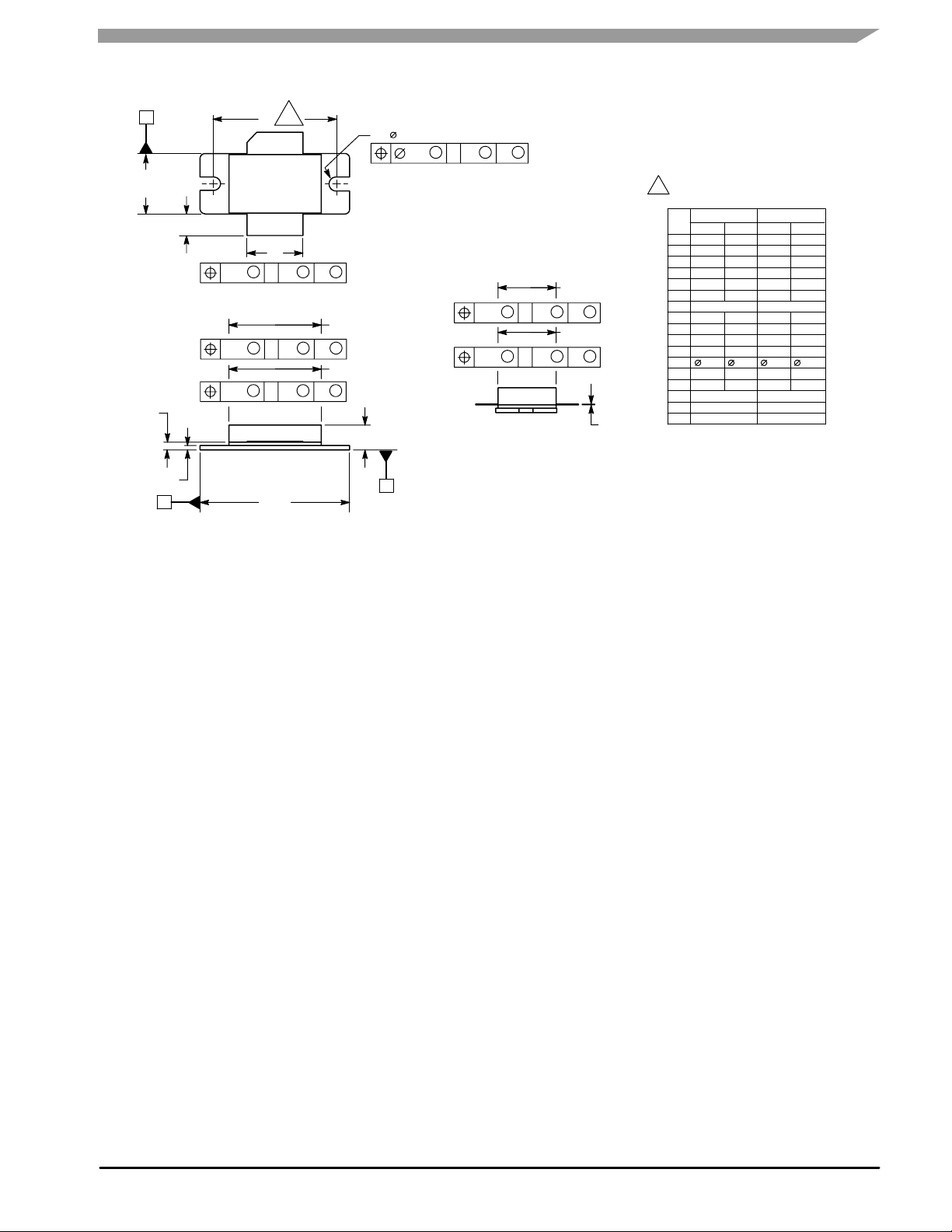
PACKAGE DIMENSIONS
N
RMATI
B
B
(FLANGE)
K
bbb B
bbb B
ccc B
H
E
AA
G
D
M
T
M
T
M
T
(FLANGE)
4
1
2
A
A
A
NOTES:
2X
Q
M
bbb B
3
M
M
(INSULATOR)
M
M
M
(LID)
N
M
M
C
SEATING
T
PLANE
M
A
T
M
ccc B
M
aaa B
M
(LID)
R
M
S
M
M
(INSULATOR)
M
F
A
T
A
T
1. DIMENSIONING AND TOLERANCING PER ANSI
Y14.5M--1994.
2. CONTROLLING DIMENSION: INCH.
3. DIMENS ION H IS MEASURED 0.030 (0.762) AWA Y
FROM PACKAGE BODY.
4. RECOMMENDED BOLT CENTER DIMENSION OF
1.16 (29.57) BASED ON M3 SCREW.
DIM MIN MAX MIN MAX
A 1.335 1.345 33.91 34.16
B 0.535 0.545 13.6 13.8
C 0.147 0.200 3.73 5.08
D 0.495 0.505 12.57 12.83
E 0.035 0.045 0.89 1.14
F 0.003 0.006 0.08 0.15
G 1.100 BSC 27.94 BSC
H 0.057 0.067 1.45 1.70
K 0.175 0.205 4.44 5.21
M 0.872 0.888 22.15 22.55
N 0.871 0.889 19.30 22.60
Q .118 .138 3.00 3.51
R 0.515 0.525 13.10 13.30
S 0.515 0.525 13.10 13.30
aaa 0.007 REF 0.178 R EF
bbb 0.010 RE F 0.254 REF
ccc 0.015 REF 0.381 R EF
STYLE 1:
PIN 1. DRAIN
2. GATE
3. SOURCE
MILLIMETERSINCHES
CASE 465B--03
ISSUE D
NI--880
HIVE INF
AR
RF Device Data
Freescale Semiconductor
RCHIVE INFORMATION
MRF18090AR3
7
Page 8

C
O
O
PRODUCT DOCUMENTATION
Refer to the following documents to aid your design process.
Engineering Bulletins
! EB212: Using Data Sheet Impedances for RF LDMOS Devices
REVISION HISTORY
The following table summarizes revisions to this document.
Revision Date Description
8
Oct. 2008 ! Modified data sheet to reflect RF Test Reduction described in Product and Process Change Notification
number, PCN12779, p. 1, 2
! Added Product Documentation and Revision History, p. 8
N
RMATI
HIVE INF
Dec. 2010 ! Data sheet archived. Part no longer manufactured.
AR
MRF18090AR3
8
RCHIVE INFORMATION
RF Device Data
Freescale Semiconductor
Page 9

C
O
O
How to Reach Us:
Home Page:
www.freescale.com
Web Support:
http://www.freescale.com/support
N
USA/Europe or Locations Not Listed:
Freescale Semiconductor, Inc.
Technical Information Center, EL516
2100 East Elliot Road
Tempe, Arizona 85284
1--800--521--6274 or +1--480--768--2130
www.freescale.com/support
Europe, Middle East, and Africa:
Freescale Halbleiter Deutschland GmbH
Technical Information Center
RMATI
Schatzbogen 7
81829 Muenchen, Germany
+44 1296 380 456 (English)
+46 8 52200080 (English)
+49 89 92103 559 (German)
+33169354848(French)
www.freescale.com/support
Japan:
Freescale Semiconductor Japan Ltd.
Headquarters
ARCO Tower 15F
1--8--1, Shimo--Meguro, Meguro--ku,
Tokyo 153--0064
Japan
0120 191014 or +81 3 5437 9125
support.japan@freescale.com
HIVE INF
Asia/Pacific:
Freescale Semiconductor China Ltd.
Exchange Building 23F
No. 118 Jianguo Road
Chaoyang District
Beijing 100022
AR
China
+86 10 5879 8000
support.asia@freescale.com
For Literature Requests O nly:
Freescale Semiconductor Literature Distribution Center
P.O. Box 5405
Denver, Colorado 80217
1--800--441--2447 or +1--303--675--2140
Fax: +1--303--675--2150
LDCForFreescaleSemiconductor@hibbertgroup.com
Information in this document is provided solely to enable system and software
implementers to use Freescale Semiconductor products. There are no express or
implied copyright licenses granted hereunder to design or fabricate any integrated
circuits or integrated circuits based on the information in this document.
Freescale Semiconductor reserves the right to make changes without further notice to
any products herein. Freescale Semiconductor makes no warranty, representation or
guarantee regarding the suitability of its products for any particular purpose, nor does
Freescale Semiconductor assume any liability arising out of the application or use of
any product or circuit, and specifically disclaims any and all liability, including without
limitation consequential or incidental damages. “T ypical” parameters that may be
provided in Freescale Semiconductor data sheets and/or specifications can and do
vary in different applications and actual performance may vary over time. All operating
parameters, including “Typicals”, must be validated for each customer application by
customer’s technical experts. Freescale Semiconductor does not convey any license
under its patent rights nor the rights of others. Freescale Semiconductor products are
not designed, intended, or authorized for use as components in systems intended for
surgical implant into the body, or other applications intended to support or sustain life,
or for any other application in which the failure of the Freescale Semiconductor product
could create a situation where personal injury or death may occur. Should Buyer
purchase or use Freescale Semiconductor products for any such unintended or
unauthorized application, Buyer shall indemnify and hold Freescale Semiconductor
and its officers, employees, subsidiaries, affiliates, and distributors harmless against all
claims, costs, damages, and expenses, and reasonable attorney fees arising out of,
directly or indirectly, any claim of personal injury or death associated with such
unintended or unauthorized use, even if such claim alleges that Freescale
Semiconductor was negligent regarding the design or manufacture of the part.
Freescalet and the Freescale logo are trademarks of Freescale Semiconductor, Inc.
All other product or service names are the property of their respective owners.
- Freescale Semiconductor, Inc. 2008, 2010. All rights reserved.
RCHIVE INFORMATION
Document Number: MRF18090A
RF Device Data
Rev. 8, 10/2008
Freescale Semiconductor
MRF18090AR3
9
 Loading...