

FREESCALE MPXH 6115AC6U Datasheet
Pressure
Freescale Semiconductor
High Temperature Accuracy
Integrated Silicon Pressure Sensor
for Measuring Absolute Pressure,
On-Chip Signal Conditioned,
Temperature Compensated and
Calibrated
The MPXxx6115A series sensor integrates on-chip, bipolar op amp
circuitry and thin film resistor networks to provide a high output signal and
temperature compensation. The small form factor and high reliability of onchip integration make the pressure sensor a logica l and economical choice
for the system designer.
The MPXxx6115A series piezoresistive transducer is a state-of-the-art,
monolithic, signal conditioned, silicon pressure sensor. This sensor combines
advanced micromachining techniques, thin film metallization, and bipolar
semiconductor processing to provide an accurate, high level analog output
signal that is proportional to applied pressure.
Features
MPXA6115A
Rev 6, 06/2010
MPXA6115A
MPXAZ6115A
MPXH6115A
MPXHZ6115A
Series
15 to 115 kPa (2.2 to 16.7 psi)
0.2 to 4.8 V Output
Application Examples
• Aviation Altimeters
• Industrial Controls
• Engine Control/Manifold Absolute
Pressure (MAP)
• Weather Station and Weather
Reporting Device Barometers
• Resistant to High Humidity and Common Automotive Media
• Improved Accuracy at High Temperature
• Available in Small and Super Small Outline Packages
• 1.5% Maximum Error over 0° to 85°C
• Ideally suited for Microprocessor or Microcontroller-Based Systems
• Temperature Compensated from -40° to +125°C
• Durable Thermoplastic (PPS) Surface Mount Package
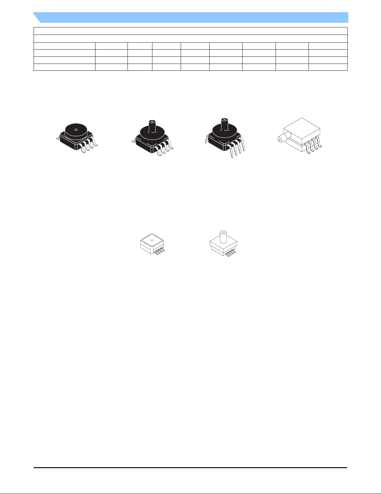
ORDERING INFORMATION
Device Name
Small Outline Package (MPXA6115A Series)
MPXA6115A6U
MPXA6115A6T1
MPXA6115AC6U
MPXA6115AC6T1
MPXA6115AC7U
Small Outline Package (Media Resistant Gel) (MPXAZ6115A Series)
MPXAZ6115A6U
MPXAZ6115AC6U
MPXAZ6115AC6T1
MPXAZ6115AP
MPXAZ6115APT1
Super Small Outline Package (MPXH6115A Series)
MPXH6115A6U
MPXH6115A6T1
MPXH6115AC6U
MPXH6115AC6T1
Case
No.
482 • • MPXA6115A
482 • • MPXA6115A
482A • • MPXA6115A
482A • • MPXA6115A
482C • • MPXA6115A
482 • • MPXAZ6115A
482A • • MPXAZ6115A
482A • • MPXAZ6115A
1369 • • MPXAZ6115A
1369 • • MPXAZ6115A
1317 • • MPXH6115A
1317 • • MPXH6115A
1317A • • MPXH6115A
1317A • • MPXH6115A
None Single Dual Gauge Differential Absolute
# of Ports Pressure Type
Device
Marking
© Freescale Semiconductor, Inc., 2007-2010. All rights reserved.
Pressure
ORDERING INFORMATION
Small Outline Package (Media Resistant Gel) (MPXHZ6115A Series)
MPXHZ6115A6U
MPXHZ6115A6T1
MPXHZ6115AC6U
MPXHZ6115AC6T1
1317 • • MPXHZ6115A
1317 • • MPXHZ6115A
1317A • • MPXHZ6115A
1317A • • MPXHZ6115A
SMALL OUTLINE PACKAGES
MPXA6115A6U/T1
MPXAZ6115A6U
CASE 482
MPXA6115AC6U/T1
MPXAZ6115AC6U/T1
CASE 482A
MPXA6115AC7U
CASE 482C
SUPER SMALL OUTLINE PACKAGES
MPXH6115A6U/T1
MPXHZ6115A6U/T1
CASE 1317
MPXH6115AC6U/T1
MPXHZ6115AC6U/T1
CASE 1317A
MPXAZ6115AP/T1
CASE 1369
MPXA6115A
Sensors
2 Freescale Semiconductor

Pressure
Operating Characteristics
Table 1. Operating Characteristics (VS = 5.0 Vdc, TA = 25°C unless otherwise noted, P1 > P2)
Characteristic Symbol Min Typ Max Unit
Pressure Range P
Supply Voltage
(1)
Supply Current I
Minimum Pressure Offset
@ V
= 5.0 Volts
S
Full Scale Output
@ V
S
Full Scale Span
@ V
S
Accuracy
(3)
= 5.0 Volts
(4)
= 5.0 Volts
(5)
(2)
(0 to 85°C)
(0 to 85°C)
(0 to 85°C)
(0 to 85°C)
OP
V
S
o
V
off
V
FSO
V
FSS
———±1.5 %V
Sensitivity V/P — 45.9 — mV/kPa
Response Time
Warm-Up Time
Offset Stability
(6)
(7)
(8)
t
R
——20—ms
——±0.25 — %V
15 — 115 kPa
4.75 5.0 5.25 Vdc
—6.010mAdc
0.133 0.200 0.268 Vdc
4.633 4.700 4.768 Vdc
4.433 4.500 4.568 Vdc
FSS
—1.0—ms
FSS
1. Device is ratiometric within this specified excitation range.
2. Offset (V
3. Full Scale Output (V
4. Full Scale Span (V
minimum rated pressure.
) is defined as the output voltage at the minimum rated pressure.
off
) is defined as the output voltage at the maximum or full rated pressure.
FSO
) is defined as the algebraic difference between the output voltage at full rated pressure and the output voltage at the
FSS
5. Accuracy is the deviation in actual output from nominal output over the entire pressure range and temperature range as a percent of span
at 25°C due to all sources of error including the following:
Linearity: Output deviation from a straight line relationship with pressure over the specified pressure range.
Temperature Hysteresis: Output deviation at any temperature within the operating temperature range, after the temperature is cycled to
and from the minimum or maximum operating temperature points, with zero differential pressure applied.
Pressure Hysteresis: Output deviation at any pressure within the specified range, when this pressure is cycled to and from minimum
or maximum rated pressure at 25°C.
TcSpan: Output deviation over the temperature range of 0° to 85°C, relative to 25°C.
TcOffset: Output deviation with minimum pressure applied, over the temperature range of 0° to 85°C, relative to 25°C.
6. Response Time is defined as the time for the incremental change in the output to go from 10% to 90% of its final value when subjected to a
specified step change in pressure.
7. Warm-up Time is defined as the time required for the product to meet the specified output voltage after the pressure has been stabilized.
8. Offset Stability is the product's output deviation when subjected to 1000 cycles of Pulsed Pressure, Temperature Cycling with Bias Test.
MPXA6115A
Sensors
Freescale Semiconductor 3

Pressure
Maximum Ratings
Table 2. Maximum Ratings
(1)
Rating Symbol Value Units
Maximum Pressure (P1 > P2) P
Storage Temperature T
Operating Temperature T
Output Source Current @ Full Scale Output
Output Sink Current @ Minimum Pressure Offset
(2)
(2)
max
stg
A
+0.5mAdc
I
o
-40° to +125°°C
-40° to +125°°C
Io--0.5mAdc
1. Exposure beyond the specified limits may cause permanent damage or degradation to the device.
2. Maximum Output Current is controlled by effective impedance from V
to Gnd or V
out
to VS in the application circuit.
out
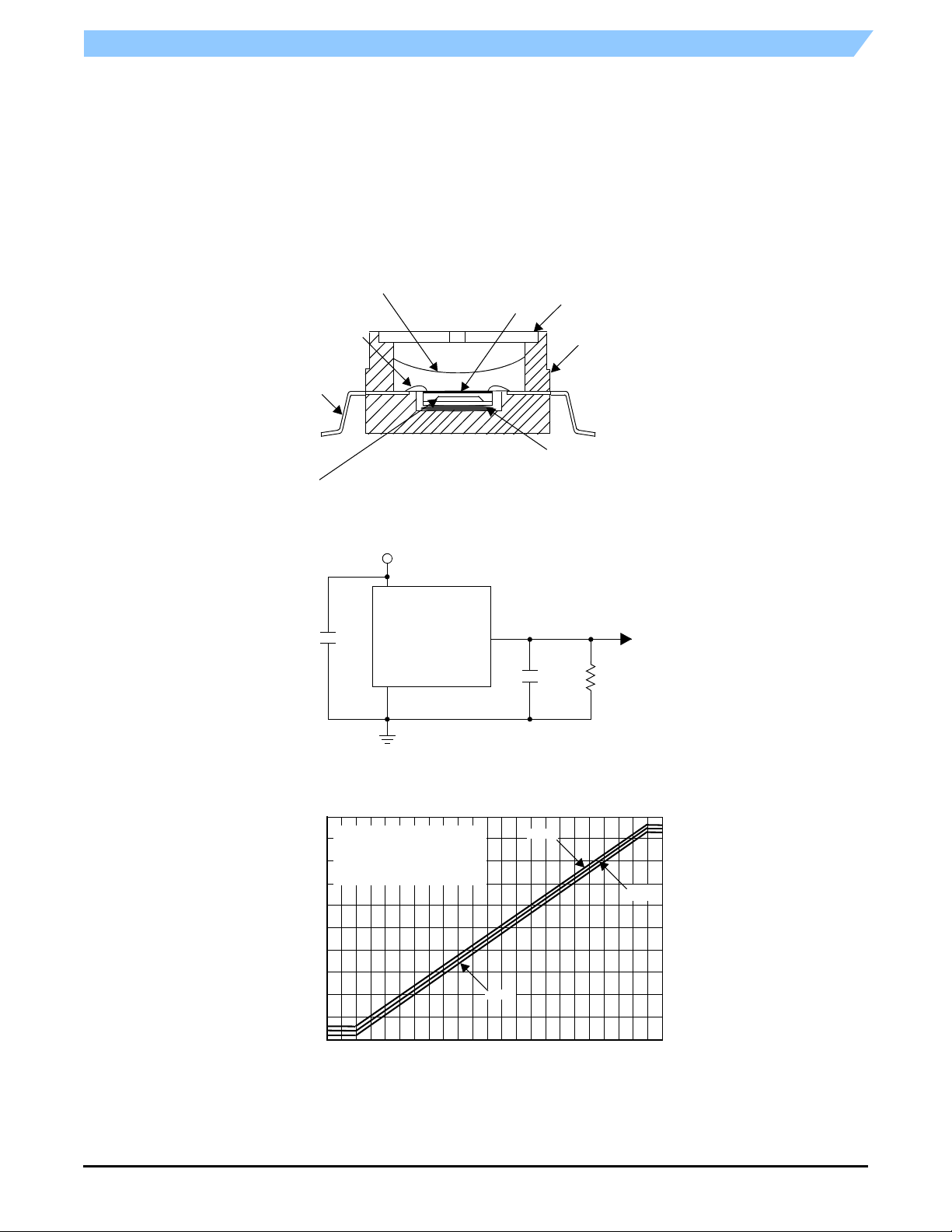
Figure 1 shows a block diagram of the internal circuitry integrated on a pressure sensor chip.
V
S
2
Sensing
Element
Thin Film
Temperature
Compensation
and
Gain Stage #1
Gain Stage #2
and Ground
Reference
Shift
Circuitry
4
400 kPa
V
OUT
3
GND
Pins 1, 5, 6, 7, and 8 are NO CONNECTS
Figure 1. Fully Integrated Pressure Sensor Schematic
MPXA6115A
Sensors
4 Freescale Semiconductor
On-chip Temperature Compensation and Calibration
Pressure
Figure 2 illustrates the absolute sensing chip in the basic
Super Small Outline chip carrier (Case 1317).
Figure 3 shows a typical application circuit (output source
current operation).
Figure 4 shows the sensor output signal relative to
pressure input. Typical minimum and maximum output
curves are shown for operation over 0° to 85°C temperature
range. The output will saturate outside of the rated pressure
range.
Fluorosilicone
Gel Die Coat
Wire Bond
Lead
Frame
Absolute Element
Sealed Vacuum Refe re n c e
Figure 2. Cross Sectional Diagram SSOP/SOP (not to scale)
+5.0 V
A fluorosilicone gel isolates the die surface and wire bonds
from the environment, while allowing the pressure signal to
be transmitted to the silicon diaphragm. The MPXxx6115A
series pressure sensor operating characteristics, internal
reliability and qualification tests are based on use of dry air as
the pressure media. Media other than dry air ma y hav e
adverse effects on sensor performance and long-term
reliability. Contact the factory for information regarding media
compatibility in your application.
Die
P1
Stainless
Steel Cap
Thermoplastic
Case
Die Bond
100 nF
5.0
4.5
4.0
3.5
3.0
2.5
2.0
Output (Volts)
1.5
1.0
0.5
0
VS Pin 2
MPXxx6115A
Pin 4
V
out
GND Pin 3
Figure 3. Typical Application Circuit
(Output Source Current Operation)
Transfer Function:
V
= Vs* (.009*P-.095) ± Error
out
V
= 5.0 Vdc
S
TEMP = 0 to 85ºC
MIN
5
101520253035404550
Pressure (ref: to sealed vacuum) in kPa
556065707580859095
MAX
47 pF
51 K
100
to ADC
TYP
110
105
115
120
Figure 4. Output vs. Absolute Pressure
MPXA6115A
Sensors
Freescale Semiconductor 5

Pressure
Transfer Function (MPXxx6115A)
Nominal Transfer Value: V
Temperature Error Band
4.0
3.0
Temperature
Error
Factor
2.0
1.0
0.0
NOTE: The Temperature Multiplier is a linear response from 0ºC to -40ºC and from 85ºC to 125ºC
Pressure Error Band
3.0
= VS x (0.009 x P - 0.095)
out
± (Pressure Error x Temp. Factor x 0.009 x VS)
VS = 5.0 ± 0.25 Vdc
MPXxxA6115A SERIES
Break Points
Temp Multiplier
- 40 3
0 to 85 1
125 1.75
-40 -20 0 20 40 60
Temperature in Cº
Error Limits for Pressure
14012010080
Pressure Error (kPa)
2.0
1.0
0.0
-1.0
-2.0
-3.0
20
40 60 80 100 120
Pressure (in kPa)
Pressure Error (Max)
15 to 115 (kPa) ±1.5 (kPa)
MPXA6115A
Sensors
6 Freescale Semiconductor
 Loading...