

Page 1
Pressure
Freescale Semiconductor
50 kPa Uncompensated
Silicon Pressure Sensors
The MPX53 series silicon piezoresistive pressure sensors provide a very
accurate and linear voltage output, directly proportional to the applied
pressure. These standard, low cost, uncompensated sensors permit
manufacturers to design and add their own external temperature
compensating and signal conditioning networks. Compensation techniques
are simplified because of the predictability of Freescale's single element
strain gauge design.
Features
• Low Cost
• Patented Silicon Shear Stress Strain Gauge Design
• Ratiometric to Supply Voltage
• Easy to Use Chip Carrier Package Options
• 60 mV Span (Typical)
• Differential and Gauge Options
MPX53
Rev 7, 05/2009
MPX53
Series
0 to 50 kPa (0 to 7.25 psi)
60 mV Full Scale Span
(Typical)
Application Examples
• Air Movement Control
• Environmental Control Systems
• Level Indicators
• Leak Detection
• Medical Instrumentation
• Industrial Controls
• Pneumatic Control Systems
• Robotics
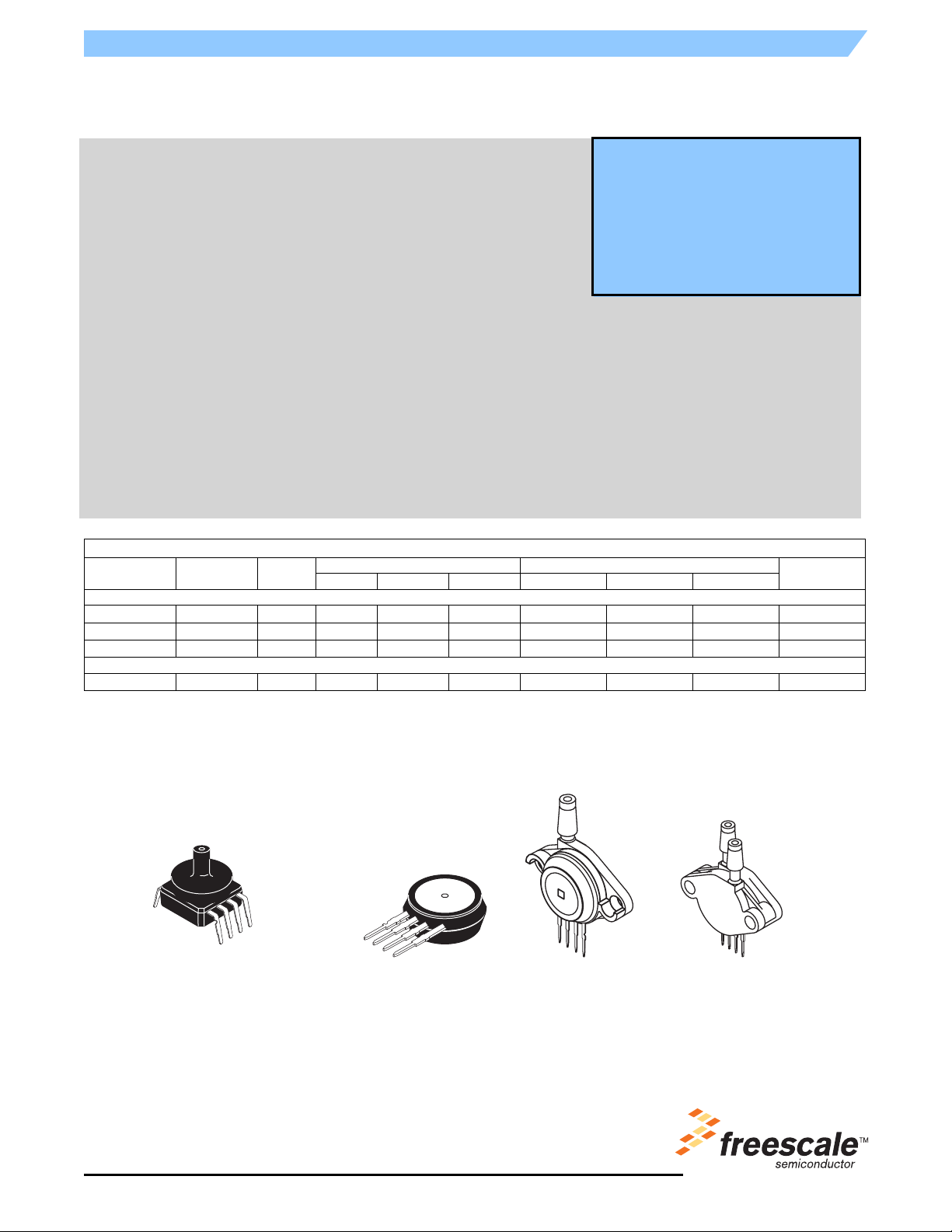
Device Name
Unibody Package (MPX53 Series)
MPX53D
MPX53DP
MPX53GP
Small Outline Package (MPXV53G Series)
MPXV53GC7U
Package
Options
Tape & Reel
Rail 344C • •
Rail 344B • •
Rail 482C • •
MPXV53GC7U
CASE 482C-03
Case
No.
344 • •
ORDERING INFORMATION
# of Ports Pressure Type
None Single Dual Gauge Differential Absolute
UNIBODY PACKAGESSMALL OUTLINE PACKAGE
MPX53D
CASE 344-15
MPX53GP
CASE 344B-01
MPX53DP
CASE 344C-01
Device
Marking
MPX53D
MPX53DP
MPX53GP
MPXV53G
© Freescale Semiconductor, Inc., 2007-2009. All rights reserved.
Page 2
Pressure
Operating Characteristics
Table 1. Operating Characteristics (VS = 3.0 Vdc, TA = 25°C unless otherwise noted, P1 > P2)
Characteristic Symbol Min Typ Max Units
Pressure Range
Supply Voltage
Supply Current I
Full Scale Span
(4)
Offset
Sensitivity ΔV/ΔΡ — 1.2 — mV/kPa
Linearity — –0.6 — 0.4 %V
Pressure Hysteresis (0 to 50 kPa) — — ±0.1 — %V
Temperature Hysteresis — — ±0.5 — %V
Temperature Coefficient of Full Scale Span TCV
Temperature Coefficient of Offset TCV
Temperature Coefficient of Resistance TCR 0.21 — 0.27 %ZIN/°C
Input Impedance Z
Output Impedance Z
Response Time
Warm-Up Time
Offset Stability
1. 1.0 kPa (kiloPascal) equals 0.145 psi.
2. Device is ratiometric within this specified excitation range. Operating the device above the specified excitation range may induce additional
error due to device self-heating.
3. Full Scale Span (V
minimum rated pressure.
4. Offset (V
5. Response Time is defined as the time for the incremental change in the output to go from 10% to 90% of its final value when subjected to a
specified step change in pressure.
6. Warm-up Time is defined as the time required for the product to meet the specified output voltage after the pressure is stabilized.
7. Offset stability is the product’s output deviation when subjected to 1000 hours of Pulsed Pressure, Temperature Cycling with Bias Test.
(1)
(2)
(3)
(5)
(10% to 90%)
(6)
(7)
) is defined as the algebraic difference between the output voltage at full rated pressure and the output voltage at the
FSS
) is defined as the output voltage at the minimum rated pressure.
OFF
V
V
P
V
OUT
OP
S
O
FSS
OFF
IN
t
R
FSS
OFF
0 — 50 kPa
— 3.0 6.0 V
— 6.0 — mAdc
45 60 90 mV
0 20 35 mV
–0.22 — -0.16 %V
— ±15 — µV/°C
355 — 505 Ω
750 — 1875 Ω
— 1.0 — ms
— — 20 — ms
— — ±0.5 — %V
DC
FSS
FSS
FSS
FSS
/°C
FSS
MPX53
Sensors
2 Freescale Semiconductor
Page 3
Maximum Ratings
Pressure
Table 2. Maximum Ratings
Maximum Pressure (P1 > P2) P
Burst Pressure (P1 > P2) P
Storage Temperature T
Operating Temperature T
1. Exposure beyond the specified limits may cause permanent damage or degradation to the device.
(1)
Rating Symbol Value Unit
MAX
Burst
STG
A
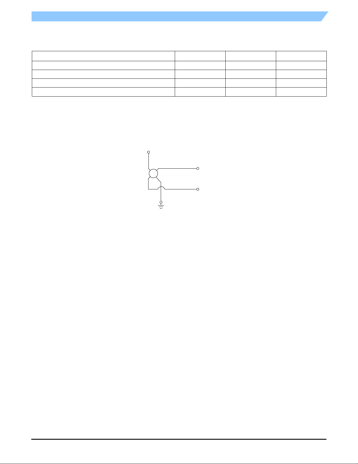
Figure 1 shows a schematic of the internal circuitry on the stand-alone pressure sensor chip.
3
+V
S
2
+V
Sensor
1
GND
OUT
4
-V
OUT
175 kPa
200 kPa
–40 to +125 °C
–40 to +125 °C
Figure 1. Uncompensated Pressure Sensor Sche ma ti c
Voltage Output versus Applied Differential Pressure
The differential voltage output of the sensor is directly
proportional to the diff ere n ti a l pressure (P1) relative to the
vacuum side (P2). Similarly, output voltage increases as
increasing vacuum is applied to the vacuum side (P2) relative
to the pressure side (P1).
MPX53
Sensors
Freescale Semiconductor 3
Page 4

Pressure
100
Temperature Compensation
Figure 2 shows the typical output characteristics of the
MPX53 series over temperature.
The piezoresistive pressure sensor element is a
semiconductor device which gives an electrical output signal
proportional to the pressure applied to the device. This device
uses a unique transverse voltage diffused semiconductor
strain gauge which is sensitive to stresses produced in a thin
silicon diaphragm by the applied pressure.
Because this strain gauge is an integral part of the silicon
diaphragm, there are no temperature effects due to
differences in the thermal expansion of the strain gauge and
the diaphragm, as are often encountered in bonded strain
gauge pressure sensors. However, the properties of the
strain gauge itself are temperature dependent, requiring that
the device be temperature compensated if it is to be used
over an extensive temperature range.
Temperature compensation and offset calibration can be
achieved rather simply with additional resistive components, or
by designing your system using the MPX2053 series sensors.
Several approaches to external temperature
compensation over –40 to +125°C and 0 to +80°C are
presented in Freescale Application Note, AN840.
LINEARITY
Linearity refers to how well a transducer's output follows
= V
the equation: V
out
+ (sensitivity x P) over the operating
off
pressure range (see Figure 3). There are two basic methods
for calculating nonlinearity: (1) end point straight line fit or
(2) a least squares best line fit. While a least squares fit gives
the “best case” linearity error (lower numerical value), the
calculations required are burdenso me .
Conversely, an end point fit will give the “worst case” error
(often more desirable in error budget calculations) and the
calculations are more straightforward for the user.
Freescale’s specified pressure sensor linearities are based
on the end point straight line method measured at the
midrange pressure.
Figure 4 illustrates the differential or gauge configuration in
the unibody chip carrier (Case 344). A silicone gel isolates the
die surface and wire bonds from the environment, while allowing
the pressure signal to be transmitted to the silicon diaphragm.
The MPX53 series pressure sensor operating
characteristics and internal reliability and qualification tests
are based on use of dry air as the pressure media. Media
other than dry air may have adverse effects on sensor
performance and long term reliability. Refer to application
note AN3728, for more information regarding media
compatibility.
MPX53
90
V
= 3 Vdc
S
80
P1 > P2
70
60
50
40
30
Output (mVdc)
20
10
0
012 34 5678
PSI
kPa
10 20 30 40 50
0
–40°C
Pressure Differential
+25°C
+125ºC
Span
Range
(Typ)
Offset
(Typ)
Figure 2. Output vs. Pressure Differential
90
80
70
Actual
60
50
40
30
Output (mVdc)
20
10
0
0MAXP
Linearity
Theoretical
Pressure (kPa)
Span
(V
FSS
Offset
(V
OFF
Silicone
Die Coat Die
)
)
OP
Wire Bond
Lead Frame
P1
P2
Stainless Steel
Metal Cover
Epoxy
Case
RTV Die
Bond
Figure 3. Linearity Specification Comparison Figure 4. Unibody Package — Cross-Sectional Diagram
(Not to Scale)
MPX53
Sensors
4 Freescale Semiconductor
Page 5

PRESSURE (P1)/VACUUM (P2) SIDE IDENTIFICATION TABLE
Freescale designates the two sides of the pressure sensor
as the Pressure (P1) side and the Vacuum (P2) side. The
Pressure (P1) side is the side containing silicone gel which
isolates the die from the environment. The Freescale MPX
pressure sensor is designed to operate with positive
differential pressure applied, P1 > P2.
The Pressure (P1) side may be identified by using the
following table.
Pressure
Part Number Case Type
MPX53D 344 Stainless Steep Cap
MPX53DP 344C Side with Port Marking
MPX53GP 344B Side with Port Attached
MPXV53 Series 482C Side with Port Attached
Pressure (P1) Side
Identifier
MPX53
Sensors
Freescale Semiconductor 5
Page 6

Pressure
PACKAGE DIMENSIONS
C
R
M
1
B
-A-
23
4
N
PIN 1
1234
L
-T-
SEATING
J
PLANE
F
D
4 PL
0.136 (0.005) T
G
M
M
A
F
DAMBAR TRIM ZONE:
THIS IS INCLUDED
WITHIN DIM. "F" 8 PL
Y
NOTES:
1.
DIMENSIONING AND TOLERANCING PER ASME
Y14.5M, 1994.
CONTROLLING DIMENSION: INCH.
2.
DIMENSION -A- IS INCLUSIVE OF THE MOLD
3.
STOP RING. MOLD STOP RING NOT TO EXCEED
Z
16.00 (0.630).
DIM MIN MAX MIN MAX
A 0.595 0.630 15.11 16.00
B 0.514 0.534 13.06 13.56
C 0.200 0.220 5.08 5.59
D 0.016 0.020 0.41 0.51
F 0.048 0.064 1.22 1.63
G 0.100 BSC 2.54 BSC
J 0.014 0.016 0.36 0.40
L 0.695 0.725 17.65 18.42
M 30˚ NOM 30˚ NOM
N 0.475 0.495 12.07 12.57
R 0.430 0.450 10.92 11.43
Y 0.048 0.052 1.22 1.32
Z 0.106 0.118 2.68 3.00
MILLIMETERSINCHES
CASE 344-15
ISSUE AA
UNIBODY PACKAGE
SEATING
PLANE
-T-
R
-A-
U
L
H
N
PORT #1
POSITIVE
PRESSURE
(P1)
B
PIN 1
12 34
-P-
0.25 (0.010) T
M
J
C
S
Q
F
G
D 4 PL
0.13 (0.005) Q
S
M
S
S
T
NOTES:
1.2.DIMENSIONING AND TOLERANCING PER ANSI
Y14.5M, 1982.
CONTROLLING DIMENSION: INCH.
2. + OUTPUT
3. + SUPPLY
MILLIMETERSINCHES
DIM MIN MAX MIN MAX
A 1.145 1.175 29.08 29.85
B 0.685 0.715 17.40 18.16
-Q-
K
S
C 0.305 0.325 7.75 8.26
D 0.016 0.020 0.41 0.51
F 0.048 0.064 1.22 1.63
G 0.100 BSC 2.54 BSC
H 0.182 0.194 4.62 4.93
J 0.014 0.016 0.36 0.41
K 0.695 0.725 17.65 18.42
L 0.290 0.300 7.37 7.62
N 0.420 0.440 10.67 11.18
P 0.153 0.159 3.89 4.04
Q 0.153 0.159 3.89 4.04
R 0.230 0.250 5.84 6.35
S
0.220 0.240 5.59 6.10
U 0.910 BSC 23.11 BSC
STYLE 1:
PIN 1. GROUND
CASE 344B-01
ISSUE B
UNIBODY PACKAGE
MPX53
Sensors
6 Freescale Semiconductor
Page 7

PACKAGE DIMENSIONS
Pressure
R
PORT #2
SEATING
PLANE
-T- -T-
V
PORT #1
U
W
L
H
-A-
PORT #2
N
VACUUM
(P2)
PORT #1
POSITIVE PRESSURE
(P1)
-Q-
SEATING
B
PLANE
PIN 1
-P-
M
0.25 (0.010) T
Q
J
C
0.13 (0.005) Q
M
T
12 43
K
S
S
F
G
D
4 PL
S
S
S
NOTES:
1.2.DIMENSIONING AND TOLERANCING PER ANSI
Y14.5M, 1982.
CONTROLLING DIMENSION: INCH.
DIM MIN MAX MIN MAX
A 1.145 1.175 29.08 29.85
B 0.685 0.715 17.40 18.16
C 0.405 0.435 10.29 11.05
D 0.016 0.020 0.41 0.51
F 0.048 0.064 1.22 1.63
G 0.100 BSC 2.54 BSC
H 0.182 0.194 4.62 4.93
J 0.014 0.016 0.36 0.41
K 0.695 0.725 17.65 18.42
L 0.290 0.300 7.37 7.62
N 0.420 0.440 10.67 11.18
P 0.153 0.159 3.89 4.04
Q 0.153 0.159 3.89 4.04
R 0.063 0.083 1.60 2.11
S
0.220 0.240 5.59 6.10
U 0.910 BSC 23.11 BSC
V 0.248 0.278 6.30 7.06
W 0.310 0.330 7.87 8.38
STYLE 1:
PIN 1. GROUND
MILLIMETERSINCHES
CASE 344C-01
ISSUE B
UNIBODY PACKAGE
CASE 482C-03
ISSUE B
SMALL OUTLINE PACKAGE
MPX53
Sensors
Freescale Semiconductor 7
Page 8

How to Reach Us:
Home Page:
www.freescale.com
Web Support:
http://www.freescale.com/support
USA/Europe or Locations Not Listed:
Freescale Semiconductor, Inc.
Technical Information Center, EL516
2100 East Elliot Road
Tempe, Arizona 85284
1-800-521-6274 or +1-480-768-2130
www.freescale.com/support
Europe, Middle East, and Africa:
Freescale Halbleiter Deutschland GmbH
Technical Information Center
Schatzbogen 7
81829 Muenchen, Germany
+44 1296 380 456 (English)
+46 8 52200080 (English)
+49 89 92103 559 (German)
+33 1 69 35 48 48 (French)
www.freescale.com/support
Japan:
Freescale Semiconductor Japan Ltd.
Headquarters
ARCO Tower 15F
1-8-1, Shimo-Meguro, Meguro-ku,
Tokyo 153-0064
Japan
0120 191014 or +81 3 5437 9125
support.japan@freescale.com
Asia/Pacific:
Freescale Semiconductor China Ltd.
Exchange Building 23F
No. 118 Jianguo Road
Chaoyang District
Beijing 100022
China
+86 010 5879 8000
support.asia@freescale.com
For Literature Requests Only:
Freescale Semiconductor Literature Distribution Center
1-800-441-2447 or +1-303-675-2140
Fax: +1-303-675-2150
LDCForFreescaleSemiconductor@hibbertgroup.com
Information in this document is provided solely to enable system and software
implementers to use Freescale Semiconductor products. There are no express or
implied copyright licenses granted hereunder to design or fabricate any integrated
circuits or integrated circuits base d on the information in this document.
Freescale Semiconductor reserves the right to make changes without further notice to
any products herein. Freescale Semiconductor makes no warranty, representation or
guarantee regarding the suitability of its products for any particular purpose, nor does
Freescale Semiconductor assume any liability arising out of the application or use of any
product or circuit, and specifically disclaims any and all liability, including without
limitation consequential or incidental damages. “Typical” parameters that may be
provided in Freescale Semiconductor data sheet s and/or specifications can and do vary
in different applications and actual performance may vary over time. All operating
parameters, including “Typicals”, must be validated for each customer application by
customer’s technical experts. Freescale Semiconductor does not convey any licen se
under its patent rights nor the rights of others. Freescale Semiconductor products are
not designed, intended, or authorized for use as components in systems intended for
surgical implant into the body, or other applications intended to support or sustain life,
or for any other application in which the failure of the Freescale Semiconduct or product
could create a situation where personal injury or death may occur. Should Buyer
purchase or use Freescale Semiconductor products for any such unintended or
unauthorized application, Buyer shall indemnify and hold Freescale Semiconductor and
its officers, employees, subsidiaries, affiliates, and distributors harmless against all
claims, costs, damages, and expenses, and reasonable attorney fees arising out of,
directly or indirectly, any claim of personal injury or death associated with such
unintended or unauthorized use, even if such claim alleges that Freescale
Semiconductor was negligent regarding the design or manufacture of the part.
Freescale™ and the Freescale logo are trademarks of Freescale Semiconductor, Inc.
All other product or service names are the property of their respective owners.
© Freescale Semiconductor, Inc. 2009. All rights reserved.
MPX53
Rev. 7
05/2009
 Loading...