


FREESCALE MPX 5100DP Datasheet

Pressure
Freescale Semiconductor
Integrated Silicon Pressure Sensor
On-Chip Signal Conditioned,
Temperature Compensated and
Calibrated
The MPX5100 series piezoresistive transducer is a state-of-the-art monolithic
silicon pressure sensor designed for a wide range of applications, but p articular ly
those employing a microcontroller or microprocessor with A/D inputs. This patented,
single element transducer combines advanced micromachining techniques, thin-film
metallization, and bipolar processing to pro v ide an accurate, high level analog
output signal that is proportional to the applied p res sure.
Features
• 2.5% Maximum Error over 0° to 85°C
• Ideally suited for Microprocessor or Microcontroller-Based Systems
• Patented Silicon Shear Stress Strain Gauge
• Available in Absolute, Differential and Gauge Configuration
• Durable Epoxy Unibody Element
• Easy-to-Use Chip Carrier Option
MPX5100
Rev 13, 05/2010
MPX5100
MPXV5100
Series
0 to 100 kPa (0 to 14.5 psi)
15 to 115 kPa (2.2 to 16.7 psi)
0.2 to 4.7 V Output
Typical Applications
• Patient Monitoring
• Process Control
• Pump/Motor Control
• Pressure Switching
Device Name
Unibody Package (MPX5100 Series)
MPX5100A 867
MPX5100AP 867B
MPX5100D 867
MPX5100DP 867C
MPX5100GP 867B
Small Outline Package (MPXV5100 Series)
MPXV5100GC6U
MPXV5100GC7U
MPXV5100DP
MPXV5100GP
Case
No.
482A • • MPXV5100G
482C • • MPXV5100G
1351 • • MPXV5100DP
1369 • • MPXV5100GP
None Single Dual Gauge Differential Absolute
ORDERING INFORMATION
# of Ports Pressure Type
• • MPX5100A
• • MPX5100AP
• • MPX5100D
• • MPX5100DP
• • MPX5100GP
Device
Marking
© Freescale Semiconductor, Inc., 2005-2010. All rights reserved.
Pressure
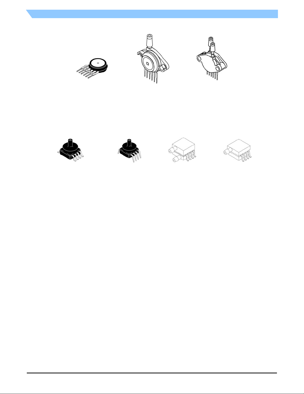
UNIBODY PACKAGES
MPX5100A/D
CASE 867-08
MPXV5100GC6U
CASE 482A-01
MPX5100AP/GP
CASE 867B-04
SMALL OUTLINE PACKAGES
MPXV5100GC7U
CASE 482C-03
MPXV5100DP
CASE 1351-01
MPX5100DP
CASE 857C-05
MPXV5100GP
CASE 1369-01
MPX5100
Sensors
2 Freescale Semiconductor

Pressure
Operating Characteristics
Table 1. Operating Characteristics (VS = 5.0 Vdc, TA = 25°C unless otherwise noted, P1 > P2. Decoupling circuit shown in
Figure 5 required to meet electrical specifications.)
Characteristic Symbol Min Typ Max Unit
Pressure Range
(1)
Gauge, Differential: MPX5100D/MPX5100G/MPXV5100G
Absolute: MPX5100A
Supply Voltage
(2)
Supply Current I
Minimum Pressure Offset
@ V
= 5.0 V
S
Full Scale Output
@ V
= 5.0 V
S
Full Scale Span
@ V
Accuracy
= 5.0 V
S
(6)
(5)
(3)
(0 to 85°C)
(4)
Differential and Absolute (0 to 85°C)
Differential and Absolute (0 to 85°C)
P
OP
V
S
O
V
OFF
V
FSO
V
FSS
0
15
—
—
100
115
4.75 5.0 5.25 V
— 7.0 10 mAdc
0.088 0.20 0.313 V
4.587 4.700 4.813 V
— 4.500 — V
— — — ±2.5 %V
Sensitivity V/P — 45 — mV/kPa
Response Time
(7)
Output Source Current at Full Scale Output I
Warm-Up Time
Offset Stability
(8)
(9)
t
O+
R
— 1.0 — ms
— 0.1 — mAdc
— — 20 — ms
— — ±0.5 — %V
kPa
DC
DC
DC
DC
FSS
FSS
1. 1.0 kPa (kiloPascal) equals 0.145 psi.
2. Device is ratiometric within this specified excitation range.
3. Offset (V
4. Full Scale Output (V
5. Full Scale Span (V
minimum rated pressure.
) is defined as the output voltage at the minimum rated pressure.
OFF
) is defined as the output voltage at the maximum or full rated pressure.
FSO
) is defined as the algebraic difference between the output voltage at full rated pressure and the output voltage at the
FSS
6. Accuracy (error budget) consists of the following:
• Linearity: Output deviation from a straight line relationship with pressure over the specified pressure range.
• Temperature Hysteresis:Output deviation at any temperature within the operating temperature range, after the temperature is cycled to
and from the minimum or maximum operating temperature points, with zero differential pressure applied.
• Pressure Hysteresis: Output deviation at any pressure within the specified range, when this pressure is cycled to and from minimum
or maximum rated pressure at 25°C.
• TcSpan: Output deviation over the temperature range of 0° to 85°C, relative to 25°C.
• TcOffset: Output deviation with minimum pressure applied over the temperature range of 0° to 85°C, relative to 25°C.
• Variation from Nominal: The variation from nominal values, for Offset or Full Scale Span, as a percent of V
at 25°C.
FSS
7. Response Time is defined as the time for the incremental changed in the output to go from 10% to 90% of its final value when subjected to
a specified step change in pressure.
8. Warm-Up Time is defined as the time required for the product to meet the specified output voltage after the Pressure has been stabilized.
9. Offset Stability is the product’s output deviation when subjected to 1000 hours of Pulsed Pressure, Temperature Cycling with Bias Test.
MPX5100
Sensors
Freescale Semiconductor 3

Pressure
Maximum Ratings
Table 2. Maximum Ratings
Maximum Pressure (P1 > P2) P
Storage Temperature T
Operating Temperature T
1.Exposure beyond the specified limits may cause permanent damage or degradation to the device.
(1)
Rating Symbol Value Unit
max
stg
A
400 kPa
-40° to +125°°C
-40° to +125°°C
Figure 1 shows a block diagram of the internal circuitry integrated on a pressure sensor chip in a Unibody Package.
V
S
3
Gain Stage #2
and
Ground
Reference
Shift Circuitry
V
out
1
Sensing
Element
GND
Thin Film
Temperature
Compensation
and
Gain Stage #1
2
Pins 4, 5, and 6 are NO CONNECTS.
Figure 1. Fully Integrated Pressure Sensor Schematic for Unibody Package Devices
Figure 2 shows a block diagram of the internal circuitry integrated on a pressure sensor chip in a Small Outline Package.
V
S
2
Gain Stage #2
and
Ground
Reference
Shift Circuitry
V
out
4
Sensing
Element
GND
Thin Film
Temperature
Compensation
and
Gain Stage #1
3
Pins 1 and 5-8 are NO CONNECTS.
Figure 2. Fully Integrated Pressure Sensor Schematic for Small Outline Package Devices
MPX5100
Sensors
4 Freescale Semiconductor

On-chip Temperature Compensation and Calibration
Pressure
Figure 3 shows the sensor output signal relative to
pressure input. Typical, minimum, and maximum output
curves are shown for operation over a temperature range of
0° to 85°C using the decoupling circuit shown in Figure 5. The
output will saturate outside of the specified pressure range.
Figure 4 illustrates both the Differential/Gauge and the
Absolute Sensing Chip in the basic chip carrier (Case 867). A
fluorosilicone gel isolates the die surface and wire bonds from
5
V
= VS*(0.009*P+0.04)
out
± (Pressure Error * Temperature Factor * 0.009 * V
VS = 5.0 V ± 0.25 Vdc
4
PE = 2.5
TM = 1
TEMP = 0 to 85°C
3
MAX
2
Output Voltage (V)
1
0
0
10
20
30
MIN
40
Pressure (kPa)
Figure 3. Output vs. Pressure Differential
Fluorosilicone
Gel Die Coat
Wire Bond
Die
Stainless Steel
Metal Cover
Epoxy Plastic
Case
the environment, while allowing the pressure signal to be
transmitted to the sensor diaphragm.
The MPX5100 series pressure sensor operating
characteristics, and internal reliability and qualification tests
are based on use of dry air as the pressure media. Media,
other than dry air, may have adverse effects on sen so r
performance and long-term reliability. Contact the factory for
information regarding media compatibility in your application.
)
S
TYP
Span Range (Typ)
Output Range (Typ)
60
50
70
80
Wire Bond
90
110
100
Fluorosilicone Gel
Die Coat
(Typ)
Offset
Die
Stainless Steel
Metal Cover
Epoxy Plastic
Case
Lead Frame
Differential/Gauge Element
Die Bond
Figure 4. Cross Sectional Diagrams (not to scale)
Figure 5 shows the recommended decoupling circuit for
interfacing the output of the integrated sensor to the A/D input
1.0 μF
0.01 μF
Figure 5. Recommended Power Supply Decoupling and Output Filtering
(For additional output filtering, please refer to Application Note AN1646.)
Lead Frame
Absolute Element
Die Bond
of a microprocessor or microcontroller. Proper decoupling of
the power supply is recommended.
+5.0 V
V
OUT
Vs
IPS
IPS
GND
OUTPUT
OUTPUT
470 pF
MPX5100
Sensors
Freescale Semiconductor 5

Pressure
Transfer Function (MPX5100D, MPX5100G, MPXV5100G
Nominal Transfer Value: V
± (Pressure Error x Temp. Mult. x 0.009 x V
V
Temperature Error Multiplier
4.0
3.0
2.0
1.0
0.0
-40 -20 0 20 40 60
Note: The Temperature Multiplier is a linear response from 0° to -40°C and from 85° to 125°C.
Pressure Error Band
3.0
= VS (P x 0.009 + 0.04)
OUT
= 5.0 V ± 0.25 V
S
)
S
MPX5100D/MPX5100G/MPXV5100G Series
Break Points
Temp Multiplier
- 40 3
0 to 85°C 1
+125° 3
Temperature in °C
MPX5100D/MPX5100G/MPXV5100G Series
Error Limits for Pressure
14012010080
Error (kPa)
2.0
1.0
0.0
-1.0
-2.0
-3.0
0 20 40 60 80 100
120
Pressure in kPa
Pressure Error (max)
0 to 100 kPa ± 2.5 kPa
MPX5100
Sensors
6 Freescale Semiconductor