

Page 1

Freescale Semiconductor
MPC885/MPC880
Hardware Specifications
MPC885EC
Rev. 3, 07/2004
This hardware specification contains detailed informatio n on
power considerations, DC/AC electrical characteristics, and AC
timing specifications for the MPC885/MPC880 (refer to Table 1
for the list of devices). The MPC885 is the superset device of the
MPC885/MPC880 family. The CPU on the MPC885/MPC880 is
a 32-bit PowerPC™ core that incorporates memory management
units (MMUs) and instruction and data caches and that
implements the PowerPC instruction set.
1Overview
The MPC885/880 is a versatile single-chip integrated
microprocessor and peripheral combination that can be used in a
variety of controller applications and communications and
networking systems. The MPC885/MPC880 provides enhanced
ATM functionality, an additional fast Ethernet controller, a USB,
and an encryption block.
Contents
1. Overview . . . . . . . . . . . . . . . . . . . . . . . . . . . . . . . . . . . 1
2. Features . . . . . . . . . . . . . . . . . . . . . . . . . . . . . . . . . . . . 2
3. Maximum Tolerated Ratings . . . . . . . . . . . . . . . . . . . 9
4. Thermal Characteristics . . . . . . . . . . . . . . . . . . . . . . 10
5. Power Dissipation . . . . . . . . . . . . . . . . . . . . . . . . . . . 10
6. DC Characteristics . . . . . . . . . . . . . . . . . . . . . . . . . . 11
7. Thermal Calculation and Measurement . . . . . . . . . . 12
8. Power Supply and Power Sequenc in g . . . . . . . . . . . 14
9. Layout Practices . . . . . . . . . . . . . . . . . . . . . . . . . . . . 15
10. Bus Signal Timing . . . . . . . . . . . . . . . . . . . . . . . . . . 15
11. IEEE 1149.1 Electrical Sp ecification s . . . . . . . . . . . 44
12. CPM Electrical Characteristics . . . . . . . . . . . . . . . . . 46
13. UTOPIA AC Electrical Specifications . . . . . . . . . . . 69
15. FEC Electrical Characteristics . . . . . . . . . . . . . . . . . 71
16. Mechanical Dat a and Ordering Information . . . . . . . 75
17. Document Revision History . . . . . . . . . . . . . . . . . . . 89
© Freescale Semiconductor, Inc., 2004. All rights reserved.
Page 2
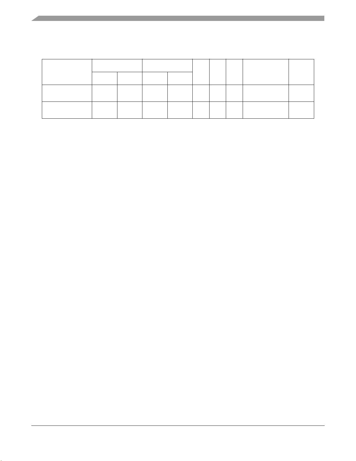
Features
Table 1 shows the functionality supported by the members of the MPC885 family.
Table 1. MPC885 Family
Cache Ethernet
Part
I Cache D Cache 10BaseT 10/100
MPC885 8 Kbyte 8 Kbyte Up to 3 2 3 2 1 Serial ATM and
MPC880 8 Kbyte 8 Kbyte Up to 2 2 2 2 1 Serial AT M and
SCC SMC USB ATM Support
UTOPIA interface
UTOPIA interface
Security
Engine
Yes
No
2Features
The MPC885/880 is comprised of three modules that each use the 32-bit internal bus: a MPC8xx core, a system
integration unit (SIU), and a communications processor module (CPM).
The following list summarizes the key MPC885/880 features:
• Embedded MPC8xx core up to 133 MHz
• Maximum frequency operation of the external bus is 80 MHz (in 1:1 mode)
— The 133-MHz core frequency supports 2:1 mode only.
— The 66-/80-MHz core frequencies support both the 1:1 and 2:1 modes.
• Single-issue, 32-bit core (compatible with the PowerPC architecture definition) with thirty-two 32-bit
general-purpose registers (GPRs)
— The core performs branch prediction with conditional prefetch and without conditional execution.
— 8-Kbyte data cache and 8-Kbyte instruction cache (see Table 1)
– Instruction cache is two-way, set-associative with 256 sets in 2 blocks
– Data cache is two-way, set-associative with 256 sets
– Cache coherency for both instruction and data caches is maintained on 128-bit (4-word) cache
blocks.
– Caches are physi cally addresse d, implement a leas t recentl y used (LRU) repl acement algori thm, and
are lockable on a cache block basis.
— MMUs with 32-entry TLB, fully associative instruction and data TLBs
— MMUs support multiple page sizes of 4, 16, and 512 Kbytes, and 8 Mbytes; 16 virtual address spaces
and 16 protection groups
— Advanced on-chip emulation debug mode
• Provides enhanced ATM functionality found on the MPC862 and MPC866 families and includes the
following:
— Improve d operation, administ ration and ma intenance (OAM) support
— OAM performance monitoring (PM) support
— Multiple APC priority levels available to support a range of traffic pace requirements
— Port-to-port switching capability without the need for RAM-based microcode
— Simultaneous MII (100BaseT) and UTOPIA (half- or full -duplex) capability
— Optional statistical cell counters per PHY
MPC885/MPC880 Hardware Specifications, Rev. 3
2 Freescale Semiconduct or
Page 3

Features
— UTOPIA L2-compliant interface with added FIFO buffering to reduce the total cell
transmission time and multi-PHY support. (The earlier UTOPIA L1 specification is also
supported.)
— Parameter RAM for both SPI and I
2
C can be relocated without RAM-based microcode
— Supports full-d uplex UTOPIA ma ster (ATM side) and slave ( PHY side) operati ons using a spl it
bus
— AAL2/VBR functionality is ROM-resident.
• Up to 32-bit data bus (dynamic bus sizing for 8, 16, and 32 bits)
• 32 address lines
• Memory controller (eight banks)
— Contains complete dynamic RAM (DRAM) controller
— Each bank can be a chip select or RAS
to support a DRAM bank.
— Up to 30 wait states programmable per memory bank
— Glueless interface to DRAM, SIMMS, SRAM, EPROMs, Flash EPROMs, and other memory
devices
— DRAM controller programmable to support most size and speed memory interfaces
— Four CAS
lines, four WE lines, and one OE line
— Boot chip-select available at reset (options for 8-, 16-, or 32-bit memory)
— Variable block sizes (32 Kbyte–256 Mbyte)
— Selectable write protection
— On-chip bus arbitration logic
• General-purpose timers
— Four 16-bit timers or two 32-bit timers
— Gate mode can enable/disable counting.
— Interrupt can be masked on reference match and event capture
• Two fast Ethernet controllers (FEC)—Two 10/100 Mbps Ethernet/IEEE 802.3 CDMA/CS that
interface through MII and/or RMII interfaces
• System integration unit (SIU)
— Bus monitor
— Software watchdog
— Periodic interrupt timer (PIT)
— Clock synthesizer
— Decrementer and time base
— Reset controller
— IEEE 1149.1 test access port (JTAG)
• Security engine is optimized to handle all the algorithms associated with IPsec, SSL/TLS, SRTP,
802.11i, and iSCSI processing. Available on the MPC885, the security engine contains a
crypto-channel, a controller, and a set of crypto hardware accelerators (CHAs). The CHAs are:
— Data encryption standard execution unit (DEU)
– DES, 3DES
– Two key (K1, K2, K1) or three key (K1, K2, K3)
– ECB and CBC modes for both DES and 3DES
MPC885/MPC880 Hardware Specifications, Rev. 3
Freescale Semiconduc tor 3
Page 4

Features
— Advanced encryption standard unit (AESU)
– Implements the Rinjdael symmetric key cipher
– ECB, CBC, and counter modes
– 128-, 192-, and 256- bit key lengths
— Message digest execution unit (MDEU)
– SHA with 160- or 256-bit message digest
– MD5 with 128-bit message digest
– HMAC with either algorithm
— Crypto-channel supporting multi-command descriptor chains
— Integrated controller managing internal resources and bus mastering
— Buffer size of 256 bytes for the DEU, AESU, and MDEU, with flow control for large data sizes
• Interrupts
— Six external interrupt request (IRQ) lines
— 12 port pins with interrupt capability
— 23 internal interrupt sources
— Programmable priority between SCCs
— Programmable highest priority request
• Communications processor module (CPM)
— RISC controller
— Communication-specifi c commands (for example,
RESTART TRANSMIT)
GRACEFUL STOP TRANSMIT, ENTER HUNT MODE, and
— Supports continuous mode transmission and reception on all serial channels
— 8-Kbytes of dual-port RAM
— Several serial DMA (SDMA) channels to support the CPM
— Three parallel I/O registers with open-drain capability
•On-chip 16
× 16 multiply accumulate controller (MAC)
— One operation per clock (two-clock latency, one-clock blockage)
— MAC operates concurrently with other instructions
— FIR loop—Four clocks per four multiplies
• Four baud rate generators
— Independent (can be connected to any SCC or SMC)
— Allow changes during operation
— Autobaud support option
• Up to three serial communication controllers (S CCs) supporting the following protocols:
— Serial ATM capability on SCCs
— Optional UTOPIA port on SCC4
— Ethernet/IEEE 802.3 optional on the SCC(s) supporting full 10-Mbps operation
— HDLC/SDLC
— HDLC bus (implements an HDLC-based local area network (LAN))
— Asynchronous HDLC to support point-to-point protocol (PPP)
MPC885/MPC880 Hardware Specifications, Rev. 3
4 Freescale Semiconduct or
Page 5

Features
—AppleTalk
— Universal asynchronous receiver transmitter (UART)
— Synchronous UART
— Serial infrared (IrDA)
— Binary synchronous communication (BISYNC)
— Totally transparent (bit streams)
— Totally transparent (frame based with optional cyclic redundancy check (CRC))
• Up to two serial management channels (SMCs) supporting the following protocols:
— UART (l ow-s peed operation)
— Transparent
— General circuit interface (GCI) controller
— Provide management for BRI devices as GCI controller in time-division multiplexed (TDM)
channels
• Universal serial bus ( USB)—Supports operation as a USB function endpoint, a USB host controller ,
or both for testing purposes (loop-back diagnostics)
— USB 2.0 full-/low-speed compatible
— The USB function mode has the following features:
– Four independent e ndpoint s suppo rt contr ol, bul k, int erru pt, and is ochrono us dat a tra nsfer s.
– CRC16 generation and checking
– CRC5 checking
– NRZI encoding/decoding with bit stuffing
– 12- or 1.5-Mbps data rate
– Flexible data buffers with multiple buffe rs per frame
– Automatic retransmission upon transmit error
— The USB host controller has the following features:
– Supports control, bulk, interrupt, and isochronous data transfers
– CRC16 generation and checking
– NRZI encoding/decoding with bit stuffing
– Supports both 12- and 1. 5-Mbps data rates (automatic g eneration of preamble tok en and data
rate configuration). Note that low-speed operation requires an external hub.
– Flexible data buffers with multiple buffe rs per frame
– Supports local loop back mode for diagnostics (12 Mbps only)
• Serial peripheral inte rface (SPI)
— Supports master and slave modes
— Supports multiple-master operation on the same bus
• Inter-integrated circuit (I
2
C) port
— Supports master and slave modes
— Supports a multiple-master environment
• Time-slot assigner (TSA)
— Allows SCCs and SMCs to run in multiplexed and/or non-multiplexed operation
— Supports T1, CEPT, PCM highway, ISDN basic rate, ISDN primary rate, user defined
MPC885/MPC880 Hardware Specifications, Rev. 3
Freescale Semiconduc tor 5
Page 6

Features
— 1- or 8-bit resolution
— Allows independent transmit and receive routing, frame synchronization, and clocking
— Allows dynamic changes
— Can be internally connected to four serial channels (two SCCs and two SMCs)
• Parallel i nterface port (PIP)
— Centronics interfa ce supp ort
— Supports fast connection between compatible ports on MPC885/880 and other MPC8xx devices
• PCMCIA interface
— Master (so cket) interface, release 2.1-compliant
— Supports two independent PCMCIA sockets
— 8 memory or I/O windows supported
• Debug interface
— Eight comparators: four operate on instruc tion address, two oper ate on data address, and two operate on
data
— Supports conditions: = ≠ < >
— Each watchpoint can generate a break point internally.
• Normal high and normal low power modes to conserve power
• 1.8-V core and 3.3-V I/O operation
• The MPC885/880 comes in a 357-pin ball grid array (PBGA) package.
MPC885/MPC880 Hardware Specifications, Rev. 3
6 Freescale Semiconduct or
Page 7
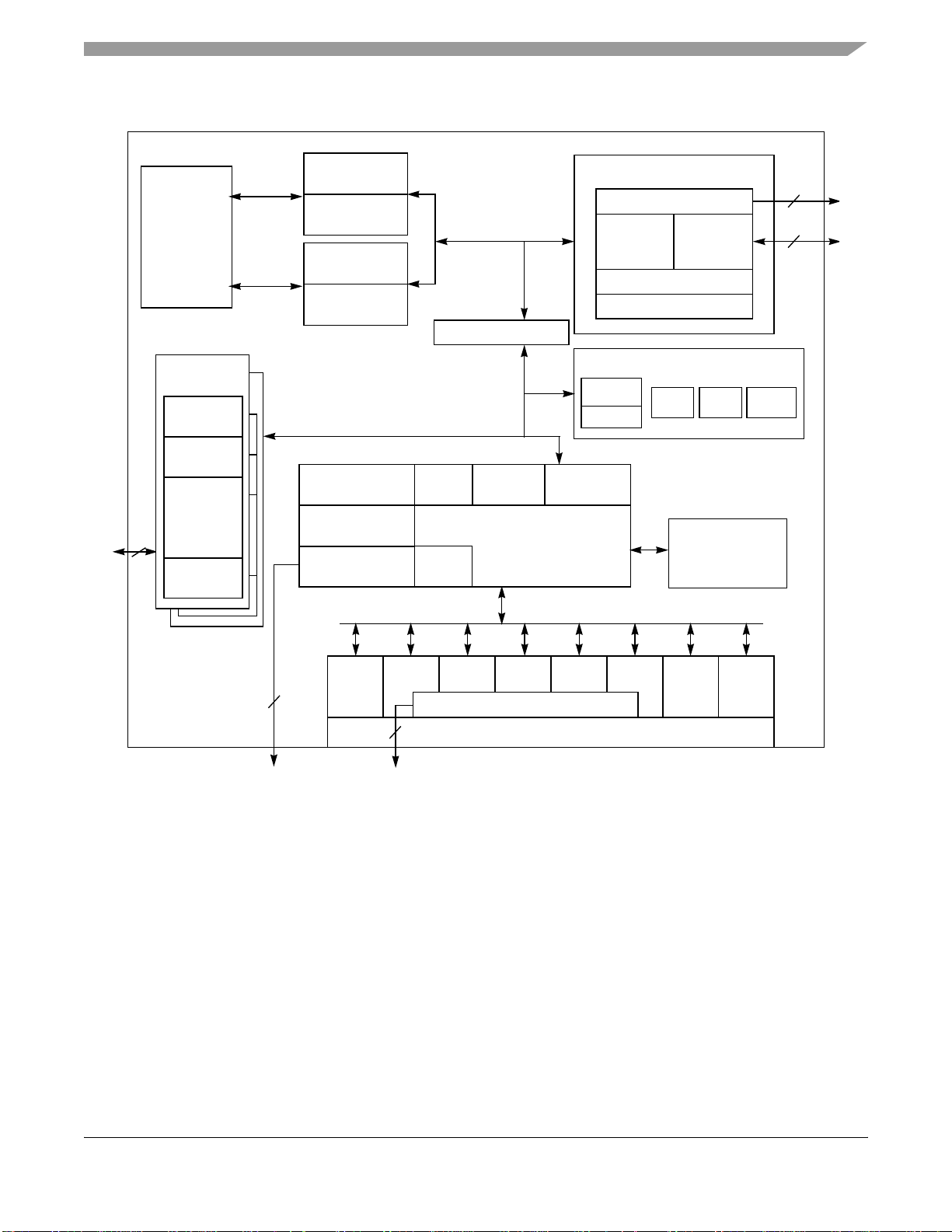
The MPC885 block diagram is shown in Figure 1.
Features
Embedded
MPC8xx
Processor
Core
Fast Ethernet
Controller
DMAs
DMAs
FIFOs
10/100
BaseT
Media Access
Control
MIII/RMII
Instruction
Bus
Load/Store
Bus
8-Kbyte
Instruction Cache
Instruction MMU
32-Entry ITLB
8-Kbyte
Data Cache
Data MMU
32-Entry DTLB
Parallel I/O
4 Baud Rate
Generators
Parallel Interface Port
Slave/Master IF
4
Interrupt
Timers
Timers
Controllers
32-Bit RISC Controller
Unified
Bus
and Program
ROM
System Interface Unit (SIU)
Bus Interface
Security Engine
Controller
Channel
8-Kbyte
Dual-Port RAM
Memory Controller
Internal
Unit
System Functions
PCMCIA-ATA Interface
External
Bus Interface
Unit
AESU DEU MDEU
Virtual IDMA
Serial DMAs
and
SCC2
SCC3 USB
SCC4/
UTOPIA
Time Slot Assigner
Serial Interface
Serial Interface
Figure 1. MPC885 Block Diagram
SPISMC2SMC1
I2C
MPC885/MPC880 Hardware Specifications, Rev. 3
Freescale Semiconduc tor 7
Page 8
Features
The MPC880 block diagram is shown in Figure 2.
Embedded
MPC8xx
Processor
Core
Fast Ethernet
Controller
DMAs
DMAs
FIFOs
10/100
BaseT
Media Access
Control
MIII/RMII
Instruction
Bus
Load/Store
Bus
8-Kbyte
Instruction Cache
Instruction MMU
32-Entry ITLB
8-Kbyte
Data Cache
Data MMU
32-Entry DTLB
Parallel I/O
4 Baud Rate
Generators
Parallel Interface Port
Slave/Master IF
4
Interrupt
Timers
Timers
Controllers
32-Bit RISC Controller
Unified
Bus
and Program
ROM
System Interface Unit (SIU)
Bus Interface
8-Kbyte
Dual-Port RAM
Memory Controller
Internal
Unit
System Functions
PCMCIA-ATA Interface
External
Bus Interface
Unit
Virtual IDMA
Serial DMAs
and
USB
SCC3
Time Slot Assigner
SCC4/
UTOPIA
Serial Interface
Serial Interface
Figure 2. MPC880 Block Diagram
SPISMC2SMC1
I2C
MPC885/MPC880 Hardware Specifications, Rev. 3
8 Freescale Semiconduct or
Page 9
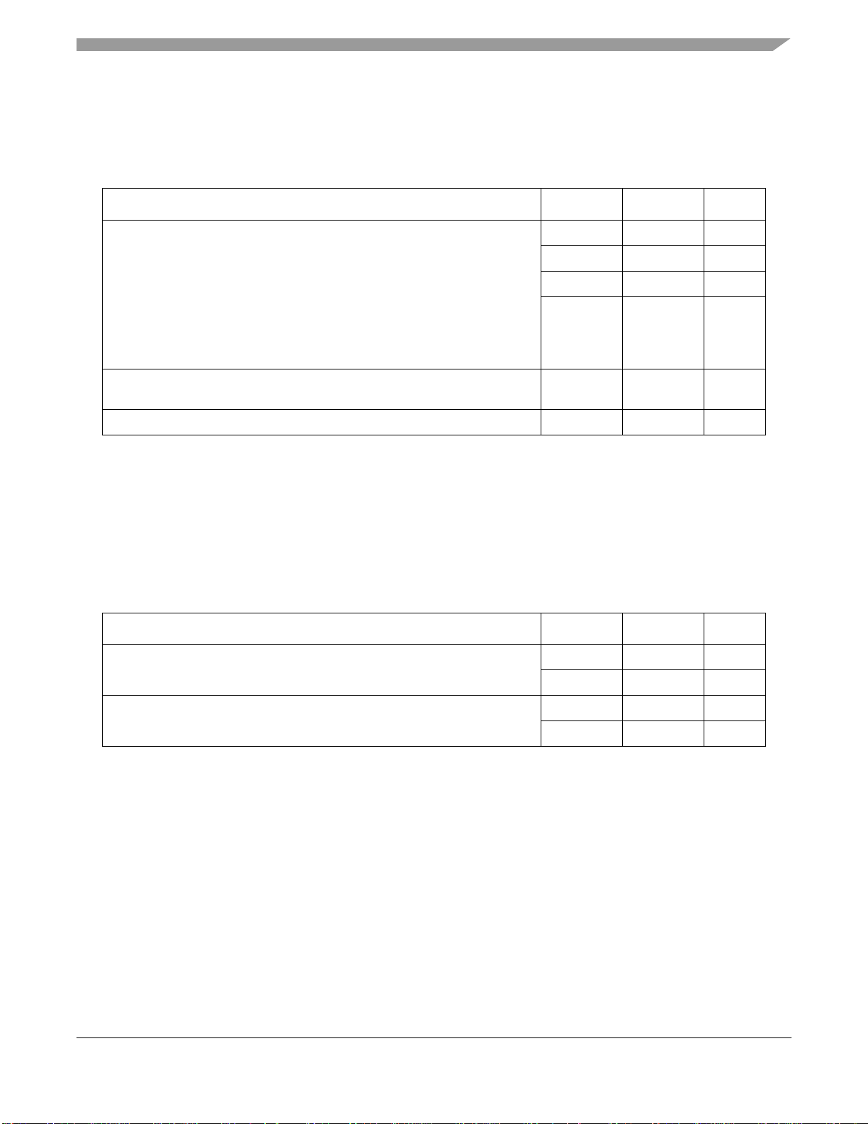
Maximum Tolerated Ratings
3 Maximum Tolerated Ratings
This section pro vides th e maximum tole rated vo ltage an d temperat ure range s for t he MPC885/8 80. Table 2
displays the maximum tolerated ratings, and Table 3 displays the operating temperatures.
Table 2. Maximum Tolerated Ratings
Symbol Value Unit
V
V
DDH
DDL
–0.3 to 4.0 V
–0.3 to 2.0 V
Supply voltage
Rating
1
VDDSYN –0.3 to 2.0 V
Difference
<100 mV
between
and
V
DDL
V
DDSYN
Input voltage
Storage temperature range T
1
The power supply of the device must start its ramp from 0.0 V.
2
Functional ope rati ng co nditions are provid ed w ith t he D C electrical specific ati ons i n Table 6. Absolute maximum
2
V
in
stg
GND – 0.3 to
V
DDH
–55 to +150 °C
ratings are stress ratings only ; functional op eration at t he maxima is not guaran teed. S tress bey ond those li sted may
affect device reliability or cause permanent damage to the device. See Sect ion8, “Power Supply and Power
Sequencing.”
Caution: All inputs that tolerate 5 V cannot be more than 2.5 V greater than VDDH. This restriction applies to power
up and normal operation (tha t is, if the MPC88 5/880 is unp owered, a volt age grea ter than 2.5 V mus t not be appli ed
to its inputs).
Table 3. Operating Temperatures
V
Rating Symbol Value Unit
1
Te mperature
Te mperature (extended) T
1
Minimum temperature s are guar anteed a s ambient te mperatu re, TA. Maximum temperatu res are guaran teed as
junction temperature, T
(standard)
T
A(min)
T
j(max)
A(min)
T
j(max)
.
j
0°C
95 °C
–40 °C
100 °C
This device contains circuitry protecting against damage due to high-static voltage or electrical fields;
however, it is advised that normal precautions be taken to avoid application of any voltages higher than
maximum-rated voltages to this high-impedance circuit. Reliability of operation is enhanced if unused
inputs are tied to an appropriate logic voltage level (for example, either GND or V
MPC885/MPC880 Hardware Specifications, Rev. 3
DD
).
Freescale Semiconduc tor 9
Page 10
Thermal Characterist ics
4 Thermal Characteristics
Table 4 shows the thermal characteristics for the MPC885/880.
Table 4. MPC885/880 Thermal Resistance Data
Rating Environment Symbol Value Unit
Junction-to-ambient
1
Natural convection Single-layer board (1s) R
Four-layer board (2s2p) R
Airflow (200 ft/min) Single-layer board (1s) R
Four-layer board (2s2p) R
Junction-to-board
Junction-to-case
Junction-to-package top
4
5
6
Natural convection Ψ
Airflow (200 ft/min) Ψ
1
Junction temperature is a function of on-chip power dissi pa tion, packa ge ther mal resis tan ce, mounting sit e (boa rd)
temperature, ambi ent tem peratu re, airfl ow, power di ssip at ion of ot her co mpone nts on th e boa rd, and boa rd therm al
resistance.
2
Per SEMI G38-87 and JEDEC JESD51-2 with the single-layer board horizontal.
3
Per JEDEC JESD51-6 with the board horizontal
4
Thermal resista nce b etw ee n t he di e a nd the printed cir cuit b oard per JEDEC JESD51 -8. Boar d te mp era t ure is
measured on the top surface of the board near the package.
5
Indicates the average thermal resist an ce be tw een the di e a nd the case top surface as me as ured by th e c ol d pl ate
method (MIL SPEC-883 Method 1012.1) with the cold pl ate temperature us ed for the c ase temperature. F or exposed
pad packages whe re the pad would be expected to be s old ere d, junction-to-case therma l res is t an ce is a si mu lated
value from the junction to the exposed pad without contact resistance.
6
Thermal characteri zatio n para meter in dicat ing the tem peratu re dif fer ence be tween p acka ge top and the junc tion
temperature per JEDEC JESD51-2.
θJA
θJMA
θJMA
θJMA
R
θJB
R
θJC
2
3
3
3
37 °C/W
25
30
22
17
10
JT
JT
2
2
5 Power Dissipation
Table 5 provides information on power dissipation. The modes are 1:1, where CPU and bus speeds are equal, and
2:1, where CPU frequency is twice bus speed.
Table 5. Power Dissipation (PD)
Die Revision
Bus
Mode
1:1
0
2:1 133 MHz 430 495 mW
1
Typical power dissipation at V
DDL
= V
= 1.8 V, and V
DDSYN
DDH
MPC885/MPC880 Hardware Specifications, Rev. 3
10 Freescale Semiconduct or
CPU
Frequency
Typical
1
Maximum
2
66 MHz 310 390 mW
80 MHz 350 430 mW
is at 3.3 V.
Unit
Page 11
2
Maximum power dissipation at V
The values in Table 5 represent V
include I/O power dissipation over V
widely by application due to buffer current, depending on external
circuitry.
DDL
= V
DDSYN
= 1.9 V, and V
NOTE
-based power diss ipati on an d d o not
DDL
DDH
is at 3.5 V.
DDH
. I/O power d issipation varies
DC Characteristics
The V
power dissipation is negligible.
DDSYN
6 DC Characteristics
Table 6 provides the DC electrical characteristics for the MPC885/880.
T able 6. DC Electrical Specifications
Characteristic Symbol Min Max Unit
Operating voltag e V
Input high voltage (all inputs except EXTAL and EXTCLK)
Input low voltage
3
2
EXTAL, EXTCLK input high voltage V
Input leakage current, Vin = 5.5 V (except TMS, TRST
DSDI pins) for 5-V tolerant pins
2
, DSCK and
(Core) 1.7 1.9 V
DDL
V
DDH
V
DDSYN
Difference
between
V
DDL
V
DDSYN
V
V
IHC
I
(I/O) 3.135 3.465 V
1
1.7 1.9 V
— 100 mV
and
IH
IL
in
2.0 3.465 V
GND 0.8 V
DD
V
DDH
0.7*(V
H
)
— 100 µA
V
Input leakage current, Vin = V
(except TMS, TRST, DSCK, and
DDH
I
In
—10µA
DSDI)
Input leakage current, Vin = 0 V (exc ept TMS, TRST
, DSCK and DSDI
I
In
—10µA
pins)
Input capacitance
4
Output high voltage, IOH = –2.0 mA,
C
in
V
OH
—20pF
2.4 — V
except XTAL and open-drain pins
Output low voltage
IOL = 2.0 mA (CLKOUT)
IOL = 3.2 mA
IOL = 5.3 mA
5
6
V
OL
—0.5V
IOL = 7.0 mA (TXD1/PA14, TXD2/PA12)
IOL = 8.9 mA (TS
1
The difference between V
2
The signals P A[0:15], PB[14:31 ], PC[4:15], PD[3:15], PE(14:31), TDI, TDO, TCK, TRST , TMS, MII1_TXEN, MII_M DIO
, TA, TEA, BI, BB, HRESET, SRESET)
DDL
and V
cannot be more than 100 mV.
DDSYN
are 5-V tolerant. The minimum voltage is still 2.0 V.
3
VIL(max) for the I2C interface is 0.8 V rather than the 1.5 V as specified in the I2C standard.
MPC885/MPC880 Hardware Specifications, Rev. 3
Freescale Semiconduc tor 11
Page 12

Thermal Calculation and Measuremen t
4
Input capaci tance is periodically sampled.
5
A(0:31), TSIZ0/REG, TSIZ1, D(0:31), IRQ(2:4), IRQ6, RD/WR, BURST, IP_B(3:7), PA(0:11), PA13, PA15, PB(14:31),
PC(4:15), PD(3:15), PE(14:31), MII1_CRS, MII_MDIO, MII1_TXEN, MII1_COL.
6
BDIP/GPL_B(5), BR, BG, FRZ/IRQ6, CS(0:7), WE(0:3), BS_A(0:3), GPL_A0/GPL_B0, OE/GPL_A1/GPL_B1,
(2:3)/GPL_B(2:3)/CS(2:3), UPWAITA/GPL_A4, UPWAITB/GPL_B4, GPL_A5, ALE_A, CE1_A, CE2_A,
GPL_A
OP(0:3) BADDR(28:30)
7 Thermal Calculation and Measurement
For the foll owing discu ssions, PD= (V
DDL
× I
) + PI/O, where PI/O is the power dissipation of the I/O drivers.
DDL
NOTE
The V
power dissipation is negligible.
DDSYN
7.1 Estimation with Junction-to-Ambient Thermal Resistance
An estimation of the chip junction temperature, TJ, in °C can be obtained from the following equation:
T
= TA + (R
J
θJA
× PD)
where:
T
= ambient temperature ºC
A
R
= package j unction-to-a mbient ther mal resistance (ºC/W)
θJA
P
= power dissipation in package
D
The junction-to-ambient thermal resistance is an industry standard value that provides a quick and easy estimation
of thermal perform ance. However , the answer is o nly an estimate; t est cases have demo nstrated that err ors of a factor
of two (in the quantity T
) are possible.
J–TA
7.2 Estimation with Junction-to-Case Thermal Resistance
Historically, thermal resistance has frequently been expressed as the sum of a junction-to-case thermal resistance
and a case-to-ambient thermal resistance:
R
= R
θJA
where:
= junction-to-ambient thermal resistance (ºC/W)
R
θJA
R
= junction-to-case thermal resistance (ºC/W)
θJC
R
= case-to-ambient thermal resistance (ºC/W)
θCA
is device-related and cannot be influenced by the user. The user adjusts the thermal environment to affect the
R
θJC
case-to-am bient therm al resistance, R
heat sink, change the mounting arrangement on the printed circuit board, or change the thermal dissipation on the
printed circuit boar d surrounding the device. Thi s thermal model is most usefu l for ceramic packages wit h heat sinks
where some 90% of the heat flows through the case and the heat sink to the ambient environment. For most
packages, a better model is required.
θJC
+ R
θCA
. For instance, the user can change the airflow around the device, add a
θCA
MPC885/MPC880 Hardware Specifications, Rev. 3
12 Freescale Semiconduct or
Page 13
Thermal Calculation and Measurement
7.3 Estimation with Junction-to-Board Thermal Resistance
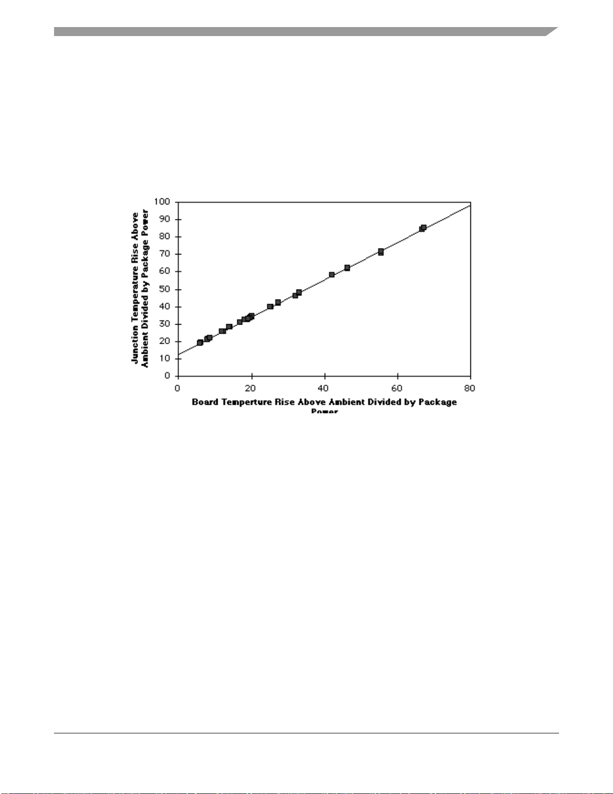
A simple package thermal model that has demonstrated reasonable accuracy (about 20%) is a two-resistor
model consisting of a junction-to-board and a junction-to-case thermal resistance. The junction-to-case
covers the situation where a heat sink is used or where a substantial amount of heat is dissipated from the
top of the package . The junct ion-to- board ther mal resi stance de scribes the ther mal perfor mance when most
of the heat is conducted to the printed circuit board. It has been observed that the thermal performance of
most plastic packages and especially PBGA packages is strongly dependent on the board temperature; see
Figure 3.
Figure 3. Effect of Board Temperature Rise on Thermal Behavior
If the board temp eratu re is known, an es timate of th e j uncti on tempe rature i n th e env ironment can b e made
using the following equation:
T
= TB + (R
J
θJB
× PD)
where:
R
= junction-to-board thermal resistance (ºC/W)
θJB
T
= board temperature ºC
B
P
= power dissipation in package
D
If the board temperature is known and the heat loss from the package case to the air can be ignored,
acceptable predicti ons of junc ti on te mper ature can be made. For this method to work, the boar d and board
mounting must be similar to the test board used to determine the junction-to-board thermal resistance,
namely a 2s2p (board with a power and a ground plane) and vias attaching the thermal balls to the ground
plane.
7.4 Estimation Using Simulation
When the board temperature is not known, a thermal simulation of the application is needed. The simple
two resistor model can be used with the thermal simulation of the application [2], or a more accurate and
complex model of the package can be used in the thermal simulation.
MPC885/MPC880 Hardware Specifications, Rev. 3
Freescale Semiconduc tor 13
Page 14

Power Supply and Power Sequencing
7.5 Experimental Determination
To determine the junction temperature of the device in the application after prototypes are available, the thermal
characterization parameter (Ψ
) can be use d to determine the junction temperature with a measurement of the
JT
temperature at the top center of the package case using the following equation:
T
= TT + (ΨJT× PD)
J
where:
Ψ
= thermal characterization parameter
JT
T
= thermocouple temperature on top of package
T
P
= power dissipation in package
D
The thermal charact erization para meter is measured pe r the JESD51-2 spec ification publ ished by JEDEC using a 40
gauge type T thermocouple epoxied to the top center of the package case. The thermocouple should be positioned
so that the thermocouple junction rests on the package. A small amount of epoxy is placed over the thermocouple
junction and over about 1 mm of wire ex tending f rom the junc tion. The ther mocouple wire is plac ed flat a gainst th e
package case to avoid measurement errors caused by the cooling effects of the thermocouple wire.
7.6 References
Semiconductor Equipment and Materials International (415) 964-5111
805 East Middlefield Rd
Mountain View, CA 94043
MIL-SPEC and EIA/JESD (JEDEC) specifications 800-854-7179 or
(Available from Global Engineering Documents) 303-397-7956
JEDEC Specifications http://www.jedec.org
1. C.E. Triplett and B. Joiner, “An Experimental Characterization of a 272 PBGA Within an Automotive Engine
Controller Module,” Proceedings of SemiTherm, San Diego, 1998, pp. 47-54.
2. B. Joiner and V. Adams, “Measurement and Simulation of Junction to Board Thermal Resistance and Its
Application in Thermal Modeling,” Proceedings of SemiTherm, San Diego, 1999, pp. 212-220.
8 Power Supply and Power Sequencing
This section pro vides design consi derations for th e MPC885/880 power supp ly . The MPC885/880 has a core voltage
(V
) and PLL voltage (V
DDL
section of the MPC885/880 is supplied with 3.3 V across V
The signals PA[0:15], PB[14:31], PC[4:15], PD[3:15], TDI, TDO, TCK, TRST_B, TMS, MII_TXEN, and
MII_MDIO are 5-V tolerant. Al l inputs cann ot be more than 2.5 V greater than V
can not exceed 5.5 V and remaining input pins cannot exceed 3.465 V. This restriction applies to power up/down
and normal operation.
One consequence of multiple power supplies is that when power is initially applied the voltage rails ramp up at
different rates. The rates depend on the nature of the power supply, the type of load on each power supply, and the
manner in which different voltages are derived. The following restrictions apply:
), which both operate at a lower voltage than the I/O voltage V
DDSYN
and VSS (GND).
DDH
DDH
. The I/O
DDH
. In addition, 5-V tolerant pins
•V
•V
14 Freescale Semiconduct or
must not exceed V
DDL
must not exceed 1.9 V, and V
DDL
DDH
MPC885/MPC880 Hardware Specifications, Rev. 3
during power up and power down.
must not exceed 3.465 V.
DDH
Page 15
Layout Practices
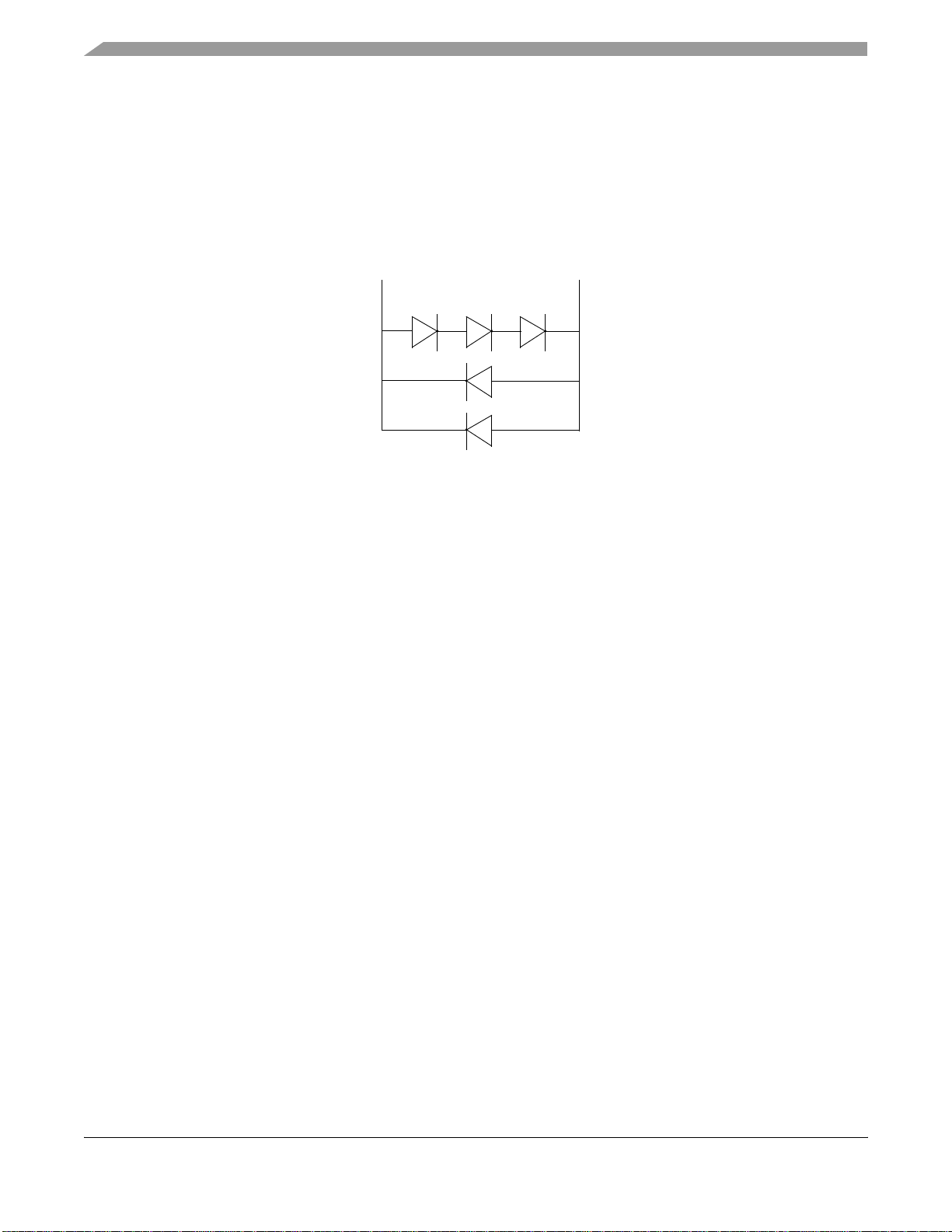
These cautions are nece ssary for th e long-t erm reliab ility of th e part. If the y are violat ed, the elect rostati c discha rge
(ESD) protection diodes are forward-biased, and excessive current can flow through these diodes. If the system
power supply design does not control the voltage sequenc ing, the circuit shown Figure 4 can be added to meet the se
requirements. The MUR420 Schott ky diodes control the maximum pote ntial difference be tween the external bus and
core power supplies on power up, and the 1N5820 diodes regulate the maximum potential difference on power
down.
V
DDH
MUR420
1N5820
Figure 4. Example Voltage Sequencing Circuit
V
DDL
9 Layout Practices
Each VDD pin on the MPC885/880 s hould be prov ided with a low-impedance p ath to the boa rd’ s supply . Each GND
pin should likewise be provid ed with a low-impe dance path to gr ound. The power su pply pins drive di stinct gro ups
of logic on chip. The V
located as close as possible to the four sides of the package. Each board designed should be characterized and
additional appropr iate decoupling cap aci tors should be used if required. The capacitor leads a nd ass oci at ed printed
circuit traces connecting to chip V
minimum, a four-layer board employing two inner layers as V
All output pins on the MPC885/880 have fast rise and fall times. Printed circuit (PC) trace interconnection length
should be minimized in order to minimize undershoot and reflections caused by these fast output switching times.
This recommendation particularly applies to the address and data buses. Maximum PC trace lengths of six inches
are recommended. Capacitan ce calculations sho uld consider all device loa ds as well as parasitic ca pacitances due to
the PC traces. Attention to proper PCB layout and bypassing becomes especially critical in systems with higher
capacitive loads bec ause these loads create hig her transient current s in the V
inputs or signals that will be inputs during reset. Special care should be taken to minimize the noise levels on the
PLL supply pins. For more information, please refer to the MPC885 User’s Manual, Section 14.4.3, “Clock
Synthesizer Power (V
power supply should be bypass ed to ground using at l east four 0.1 µF by-pass capacitors
DD
and GND should be kept to less than half an inch per capacitor lead. At a
DD
and GND planes should be used.
DD
and GND circuits. Pull up all unused
DD
DDSYN
, V
SSSYN
, V
SSSYN1
)”.
10 Bus Signal Timing
The maximum bus speed supported by the MPC885/880 is 80 MHz. Higher-speed parts must be operated in
half-speed bus mode (fo r example, an MPC885/880 used at 133 MHz must be configured f or a 66 MHz bus). Table 7
shows the frequency ra nges for standard part frequen cies in 1:1 bus mode, and Table 8 shows the frequency rang es
for standard part frequencies in 2:1 bus mode.
MPC885/MPC880 Hardware Specifications, Rev. 3
15 Freescale Semiconduct or
Page 16
Bus Signal Timing
Table 7. Frequency Ranges for Standard Part Frequencies (1:1 Bus Mode)
Part Frequency 66 MHz 80 MHz
Min Max Min Max
Core frequency 40 66.67 40 80
Bus frequency 40 66.67 40 80
Table 8. Frequency Ranges for Standard Part Frequencies (2:1 Bus Mode)
Part Frequenc y 66 MHz 80 MHz 133 MHz
Min Max Min Max Min Max
Core frequency 40 66.67 40 80 40 133
Bus frequency 20 33.33 20 40 20 66
Table 9 provides the timings for the MPC885/880 at 33-, 40-, 66-, and 80-MHz bus operation.
The timing for the MPC885/880 bus shown assumes a 50-pF load f or maximum delays and a 0-pF load for minimum
delays. CLKOUT assumes a 100-pF load maximum delay.
Table 9. Bus Operation Timings
33 MHz 40 MHz 66 MHz 80 MHz
Num Characteristic
Min Max Min Max Min Max Min Max
B1 Bus period ( CLKOUT), see Table 7 ————————ns
B1a EXTCLK to CLKOUT phase skew - If
CLKOUT is an integer multiple of
EXTCLK, then the rising edge of EXTCLK
is aligned with th e rising edge of CLKO UT .
For a non-integer m ultiple of EXTCLK, this
synchronization is lost, and the rising
edges of EXTCLK and CLKOUT have a
continuously varying phase skew.
B1b CLKOUT frequency jitter pea k-to -peak — 1 — 1 — 1 — 1 ns
B1c Frequency jitter on EXTCLK — 0.50 — 0.50 — 0.50 — 0.50 %
B1d CLKOUT phase jitter peak-to-peak
for OSCLK ≥ 15 MHz
CLKOUT phase jitter peak-to-peak
for OSCLK < 15 MHz
B2 CLKOUT pulse width low
(MIN = 0.4
B3 CLKOUT pulse width high
(MIN = 0.4
× B1, MAX = 0.6 × B1)
× B1, MAX = 0.6 × B1)
–2 +2 –2 +2 –2 +2 –2 +2 ns
—4—4—4—4ns
—5 – 5—5—5ns
12.1 18.2 10.0 15.0 6.1 9.1 5.0 7.5 ns
12.1 18.2 10.0 15.0 6.1 9.1 5.0 7.5 ns
Unit
B4 CLKOUT rise time — 4.00 — 4.00 — 4.00 — 4.00 ns
B5 CLKOUT fall time
16 Freescale Semiconduct or
MPC885/MPC880 Hardware Specifications, Rev. 3
— 4.00 — 4.00 — 4.00 — 4.00 ns
Page 17

Bus Signal Timing
Num Characteristic
Table 9. Bus Operation Timings (continued)
33 MHz 40 MHz 66 MHz 80 MHz
Unit
Min Max Min Max Min Max Min Max
B7 CLKOUT to A(0:31), BADDR(28:30),
RD/WR
(MIN = 0.25
B7a CLKOUT to TSIZ(0:1), REG, RSV, BDIP,
PTR output hold (MIN = 0.25
B7b CLKOUT to BR, BG, FRZ, VFLS(0:1),
VF(0:2) IWP(0:2), LWP(0:1), STS
hold (MIN = 0.25
B8 CLKOUT to A(0:31), BADDR(28:30)
RD/WR
(MAX = 0.25
B8a CLKOUT to TSIZ(0:1), REG, RSV, AT(0:3)
BDIP
B8b CLKOUT to BR, BG, VFLS(0:1), VF(0:2),
IWP(0:2), FRZ, LWP(0:1), STS
(MAX = 0.25 × B1 + 6.3)
B9 CLKOUT to A(0:31), BADDR(28:30),
RD/WR
RSV
(MAX = 0.25
B1 1 CLKOUT to TS, BB assertion
(MAX = 0.25
, BURST, D(0:31) output hold
× B1)
× B1)
output
× B1)
, BURST, D(0:31) valid
× B1 + 6.3)
, PTR valid (MAX = 0.25 × B1 + 6.3)
4
valid
, BURST , D(0:31), TSIZ(0:1), REG ,
, AT(0:3), PTR High-Z
× B1 + 6.3)
× B1 + 6.0)
7.60 — 6.30 — 3.80 — 3.13 — ns
7.60 — 6.30 — 3.80 — 3.13 — ns
7.60 — 6.30 — 3.80 — 3.13 — ns
—13.80—12.50—10.00— 9.43 ns
—13.80—12.50—10.00— 9.43 ns
—13.80—12.50—10.00— 9.43 ns
7.60 13.80 6.30 12.50 3.80 10.00 3.13 9.43 ns
7.60 13.60 6.30 12.30 3.80 9.80 3.13 9.13 ns
B1 1a CLKOUT to TA, BI assertion (when driven
by the memory controller or PCMCIA
interface) (MAX = 0.00 × B1 + 9.30 1)
B12 CLKOUT to TS, BB negation
(MAX = 0.25
B12a CLKOUT to TA, BI negation (when driven
by the memory controller or PCMCIA
interface) (MAX = 0.00 × B1 + 9.00)
B13 CLKOUT to TS, BB High-Z
(MIN = 0.25
B13a CLKOUT to T A, BI High-Z (whe n driven by
the memory controller or PCMCIA
interface) (MIN = 0.00× B1 + 2.5)
B14 CLKOUT to TEA assertion
(MAX = 0.00
B15 CLKOUT to TEA High-Z (MIN = 0.00 × B1
+ 2.50)
B16 TA
, BI valid to CLKOUT (setup time)
(MIN = 0.00
× B1 + 4.8)
× B1)
× B1 + 9.00)
× B1 + 6.00)
2.50 9.30 2.50 9.30 2.50 9.30 2.50 9.30 ns
7.60 12.30 6.30 11.00 3.80 8.50 3.13 7.92 ns
2.50 9.00 2.50 9.00 2.50 9.00 2.5 9.00 ns
7.60 21.60 6.30 20.30 3.80 14.00 3.13 12.93 ns
2.50 15.00 2.50 15.00 2.50 15.00 2.5 15.00 ns
2.50 9.00 2.50 9.00 2.50 9.00 2.50 9.00 ns
2.50 15.00 2.50 15.00 2.50 15.00 2.50 15.00 ns
6.00 — 6.00 — 6.00 — 6 — ns
MPC885/MPC880 Hardware Specifications, Rev. 3
17 Freescale Semiconduct or
Page 18
Bus Signal Timing
Num Characteristic
Table 9. Bus Operation Timings (continued)
33 MHz 40 MHz 66 MHz 80 MHz
Unit
Min Max Min Max Min Max Min Max
B16a TEA, KR, RETRY, CR valid to CLKOUT
(setup time) (MIN = 0.00
B16b BB, BG, BR, valid to CLKOUT (setup time)
2
(4MIN = 0.00 × B1 + 0.00)
B17 CLKOUT to T A, TEA, BI , BB, BG, BR valid
(hold time) (MIN = 0.00
× B1 + 4.5)
× B1 + 1.00
3
)
B17a CLKOUT to KR, RETRY, CR valid (hold
time) (MIN = 0.00
B18 D(0:31) valid to CLKOUT rising edge
(setup time)
B19 CLKOUT rising edge to D (0:31) valid (hold
4
(MIN = 0.00 × B1 + 1.00 5)
time)
B20 D(0:31) valid to CLKOUT falling edge
(setup time)
B21 CLKOUT falling edge to D(0:31) valid
(hold time)
× B1 + 2.00)
4
(MIN = 0.00 × B1 + 6.00)
6
(MIN = 0.00 × B1 + 4.00)
6
(MIN = 0.00 × B1 + 2.00)
B22 CLKOUT rising edge to CS asserted
GPCM ACS = 00 (MAX = 0.25 × B1 + 6.3)
B22a CLKOUT falling edge to CS
asserted
GPCM ACS = 10, TRLX = 0
(MAX = 0.00 × B1 + 8.00)
4.50 — 4.50 — 4.50 — 4.50 — ns
4.00 — 4.00 — 4.00 — 4.00 — ns
1.00 — 1.00 — 2.00 — 2.00 — ns
2.00 — 2.00 — 2.00 — 2.00 — ns
6.00 — 6.00 — 6.00 — 6.00 — ns
1.00 — 1.00 — 2.00 — 2.00 — ns
4.00 — 4.00 — 4.00 — 4.00 — ns
2.00 — 2.00 — 2.00 — 2.00 — ns
7.60 13.80 6.30 12.50 3.80 10.00 3.13 9.43 ns
— 8.00 — 8.00 — 8.00 — 8.00 ns
B22b CLKOUT falling edge to CS assert ed
GPCM ACS = 11, TRLX = 0, EBDF = 0
(MAX = 0.25 × B1 + 6.3)
B22c CLKOUT falling edge to CS asserted
GPCM ACS = 11, TRLX = 0, EBDF = 1
(MAX = 0.375 × B1 + 6.6)
B23 CLKOUT rising edge to CS
negated
GPCM read access, GPCM write access
ACS = 00, TRLX = 0 and CSNT = 0
(MAX = 0.00 × B1 + 8.00)
B24 A(0:31) and BADDR(28:30) to CS
asserted GPC M ACS = 10, TRLX = 0
(MIN = 0.25 × B1 – 2.00)
B24a A(0:31) and BADDR(28:30) to CS
asserted GPCM ACS = 11 TRLX = 0
(MIN = 0.50 × B1 – 2.00)
B25 CLKOUT rising edge to OE, WE(0:3)
asserted (MAX = 0.00 × B1 + 9.00)
B26 CLKOUT rising edge to OE
(MAX = 0.00
× B1 + 9.00)
negated
MPC885/MPC880 Hardware Specifications, Rev. 3
7.60 13.80 6.30 12.50 3.80 10.00 3.13 9.43 ns
10.90 18.00 10.90 16.00 5.20 12.30 4.69 10.93 ns
2.00 8.00 2.00 8.00 2.00 8.00 2.00 8.00 ns
5.60 — 4.30 — 1.80 — 1.13 — ns
13.20 — 10.50 — 5.60 — 4.25 — ns
— 9.00 — 9.00 — 9.00 — 9.00 ns
2.00 9.00 2.00 9.00 2.00 9.00 2.00 9.00 ns
18 Freescale Semiconduct or
Page 19

Bus Signal Timing
Num Characteristic
Table 9. Bus Operation Timings (continued)
33 MHz 40 MHz 66 MHz 80 MHz
Unit
Min Max Min Max Min Max Min Max
B27 A(0:31) and BADDR(28:30) to CS
asserted GPC M ACS = 10, TRLX = 1
(MIN = 1.25 × B1 – 2.00)
B27a A(0:31) and BADDR(28:30) to CS
asserted GPCM ACS = 11, TRLX = 1
(MIN = 1.50 × B1 – 2.00)
B28 CLKOUT rising edge to WE(0:3) negated
GPCM write access CSNT = 0
(MAX = 0.00 × B1 + 9.00)
B28a CLKOUT fa lling ed ge to WE
GPCM write access TRLX = 0, CSNT = 1,
EBDF = 0 (MAX = 0.25 × B1 + 6.80)
B28b CLKOUT falling edge to CS negate d
GPCM write access TRLX = 0, CSNT = 1
ACS = 10 or ACS = 11, EBDF = 0
(MAX = 0.25 × B1 + 6.80)
B28c CLKOUT falli ng edge to WE
GPCM write access TRLX = 0, CSNT = 1
write access TRLX = 0, CSNT = 1,
EBDF = 1 (MAX = 0.375 × B1 + 6.6)
B28d CLKOUT falling edge to CS
GPCM write access TRLX = 0, CSNT = 1,
ACS = 10, or ACS = 11, EBDF = 1
(MAX = 0.375 × B1 + 6.6)
(0:3) negated
(0:3) negated
negated
35.90 — 29.30 — 16.90 — 13.60 — ns
43.50 — 35.50 — 20.70 — 16.75 — ns
— 9.00 — 9.00 — 9.00 — 9.00 ns
7.60 14.30 6.30 13.00 3.80 10.50 3.13 9.93 ns
—14.30—13.00—10.50— 9.93 ns
10.90 18.00 10.90 18.00 5.20 12.30 4.69 11.29 ns
— 18.00 — 18.00 — 12.30 — 11.30 ns
B29 WE
B29a WE(0:3) neg ated to D(0:31) High-Z GPCM
B29b CS
B29c CS negated to D (0:31) High-Z GPCM write
B29d WE
B29e CS neg ated to D(0:31) High-Z G PCM write
(0:3) negated to D(0:31) Hi gh-Z GPCM
write access, CSNT = 0, EBDF = 0
(MIN = 0.25 × B1 – 2.00)
write access, TRLX = 0, CSNT = 1,
EBDF = 0 (MIN = 0.50 × B1 – 2.00)
negated to D(0:31) High-Z GPCM write
access, ACS = 00, TRLX = 0 & CSNT = 0
(MIN = 0.25 × B1 – 2.00)
access, TRLX = 0, CSNT = 1, ACS = 10,
or ACS = 11 EBDF = 0
(MIN = 0.50 × B1 – 2.00)
(0:3) negated to D(0:31) Hi gh-Z GPCM
write access, TRLX = 1, CSNT = 1,
EBDF = 0 (MIN = 1.50 × B1 – 2.00)
access, TRLX = 1, CSNT = 1, ACS = 10,
or ACS = 11 EBDF = 0
(MIN = 1.50 × B1 – 2.00)
MPC885/MPC880 Hardware Specifications, Rev. 3
5.60 — 4.30 — 1.80 — 1.13 — ns
13.20 — 10.50 — 5.60 — 4.25 — ns
5.60 — 4.30 — 1.80 — 1.13 — ns
13.20 — 10.50 — 5.60 — 4.25 — ns
43.50 — 35.50 — 20.70 — 16.75 — ns
43.50 — 35.50 — 20.70 — 16.75 — ns
19 Freescale Semiconduct or
Page 20
Bus Signal Timing
Num Characteristic
Table 9. Bus Operation Timings (continued)
33 MHz 40 MHz 66 MHz 80 MHz
Unit
Min Max Min Max Min Max Min Max
B29f WE(0:3) neg ated to D(0:31) High-Z GPCM
write access, TRLX = 0, CSNT = 1,
EBDF = 1 (MIN = 0.375 × B1 – 6.30)
B29g CS neg ated to D(0:31) High-Z G PCM write
access, TRLX = 0, CSNT = 1 ACS = 10 or
ACS = 11, EBDF = 1
(MIN = 0.375 × B1–6.30)
B29h WE
(0:3) negated to D(0:31) Hi gh-Z GPCM
write access, TRLX = 1, CSNT = 1,
EBDF = 1 (MIN = 0.375 × B1 – 3.30)
B29i CS negated to D (0:31) High-Z GPCM write
access, TRLX = 1, CSNT = 1, ACS = 10 or
ACS = 11, EBDF = 1
(MIN = 0.375 × B1–3.30)
B30 CS
, WE(0:3) negated to A(0:31),
BADDR(28:30) Invalid GPCM write
access
7
(MIN = 0.25 × B1–.00)
B30a WE(0:3) negated to A(0:31),
BADDR(28:30) Invalid GPCM, write
access, TRLX = 0, CSNT = 1, CS negated
to A(0:31) invalid GPCM write access
TRLX = 0, CSNT =1 ACS = 10, or
ACS == 11, EBDF = 0
(MIN = 0.50 × B1 – 2.00)
5.00 — 3.00 — 0.00 — 0.00 — ns
5.00 — 3.00 — 0.00 — 0.00 — ns
38.40 — 31.10 — 17.50 — 13.85 — ns
38.40 — 31.10 — 17.50 — 13.85 — ns
5.60 — 4.30 — 1.80 — 1.13 — ns
13.20 — 10.50 — 5.60 — 4.25 — ns
B30b WE
BADDR(28:30) invalid GPCM write
access, TRLX = 1, CSNT = 1. CS negated
to A(0:31) invalid GPCM write access
TRLX = 1, CSNT = 1, ACS = 10, or
ACS == 11 EBDF = 0
(MIN = 1.50 × B1 – 2.00)
B30c WE
BADDR(28:30) invalid GPCM write
access, TRLX = 0, CSNT = 1. CS negated
to A(0:31) invalid GPCM write access,
TRLX = 0, CSNT = 1 ACS = 10,
ACS == 11, EBDF = 1
(MIN = 0.375 × B1–3.00)
B30d WE
BADDR(28:30) invalid GPCM write access
TRLX = 1, CSNT =1, CS negated to
A(0:31) inv alid GPCM writ e access
TRLX = 1, CSNT = 1, ACS = 10 or 11,
EBDF = 1
(0:3) negated to A(0:3 1) invalid GPCM
(0:3) negated to A(0:31),
(0:3) negated to A(0:31),
MPC885/MPC880 Hardware Specifications, Rev. 3
43.50 — 35.50 — 20.70 — 16.75 — ns
8.40 — 6.40 — 2.70 — 1.70 — ns
38.67 — 31.38 — 17.83 — 14.19 — ns
20 Freescale Semiconduct or
Page 21

Bus Signal Timing
Num Characteristic
Table 9. Bus Operation Timings (continued)
33 MHz 40 MHz 66 MHz 80 MHz
Unit
Min Max Min Max Min Max Min Max
B31 CLKOUT falling edge to CS valid, as
requested by control bit CST4 in the
corresponding word in the UPM
(MAX = 0.00 × B1 + 6.00)
B31a CLKOUT falling edge to CS
requested by control bit CST1 in the
corresponding word in the UPM
(MAX = 0.25 × B1 + 6.80)
B31b CLKOUT rising edge to CS
requested by control bit CST2 in the
corresponding word in the UPM
(MAX = 0.00 × B1 + 8.00)
B31c CLKOUT rising edge to CS
requested by control bit CST3 in the
corresponding word in the UPM
(MAX = 0.25 × B1 + 6.30)
B31d CLKOUT falling edge to CS
requested by control bit CST1 in the
corresponding word in the UPM EBDF = 1
(MAX = 0.375 × B1 + 6.6)
B32 CLKOUT falling edge to BS
requested by control bit BST4 in the
corresponding word in the UPM
(MAX = 0.00 × B1 + 6.00)
valid, as
valid, as
valid, as
valid, as
valid, as
1.50 6.00 1.50 6.00 1.50 6.00 1.50 6.00 ns
7.60 14.30 6.30 13.00 3.80 10.50 3.13 10.00 ns
1.50 8.00 1.50 8.00 1.50 8.00 1.50 8.00 ns
7.60 13.80 6.30 12.50 3.80 10.00 3.13 9.40 ns
13.30 18.00 11.30 16.00 7.60 12.30 4.69 11.30 ns
1.50 6.00 1.50 6.00 1.50 6.00 1.50 6.00 ns
B32a CLKOUT falling edge to BS
requested by control bit BST1 in the
corresponding word in the UPM, EBDF = 0
(MAX = 0.25 × B1 + 6.80)
B32b CLKOUT rising edge to BS
requested by control bit BST2 in the
corresponding word in the UPM
(MAX = 0.00 × B1 + 8.00)
B32c CLKOUT rising edge to BS
requested by control bit BST3 in the
corresponding word in the UPM
(MAX = 0.25 × B1 + 6.80)
B32d CLKOUT falling edge to BS
requested by control bit BST1 in the
corresponding word in the UPM, EBDF = 1
(MAX = 0.375 × B1 + 6.60)
B33 CLKOUT falling edge to GPL
requested by control bit GxT4 in the
corresponding word in the UPM
(MAX = 0.00 × B1 + 6.00)
MPC885/MPC880 Hardware Specifications, Rev. 3
valid, as
valid, as
valid, as
valid, as
valid, as
7.60 14.30 6.30 13.00 3.80 10.50 3.13 10.00 ns
1.50 8.00 1.50 8.00 1.50 8.00 1.50 8.00 ns
7.60 14.30 6.30 13.00 3.80 10.50 3.13 10.00 ns
13.30 18.00 11.30 16.00 7.60 12.30 4.49 11.30 ns
1.50 6.00 1.50 6.00 1.50 6.00 1.50 6.00 ns
21 Freescale Semiconduct or
Page 22

Bus Signal Timing
Num Characteristic
Table 9. Bus Operation Timings (continued)
33 MHz 40 MHz 66 MHz 80 MHz
Unit
Min Max Min Max Min Max Min Max
B33a CLKOUT rising edge to GPL valid, as
requested by control bit GxT3 in the
corresponding word in the UPM
(MAX = 0.25 × B1 + 6.80)
B34 A(0:31), BADDR(28:30), and D(0:31) to
CS valid, as requested by control bi t CST4
in the corresponding word in the UPM
(MIN = 0.25 × B1 – 2.00)
B34a A(0:31), BADDR(28:30), and D(0:31) to
valid, as requested by control bi t CST1
CS
in the corresponding word in the UPM
(MIN = 0.50 × B1 – 2.00)
B34b A(0:31), BADDR(28:30), and D(0:31) to
valid, as requested by CST2 in the
CS
corresponding word in UPM
(MIN = 0.75 × B1 – 2.00)
B35 A(0:31), BADDR(28:30) to CS
valid, as
requested by control bit BST4 in the
corresponding word in the UPM
(MIN = 0.25 × B1 – 2.00)
B35a A(0:31), BADDR(28:30), and D(0:31) to
BS valid, as requested by BST1 in the
corresponding word in the UPM
(MIN = 0.50 × B1 – 2.00)
7.60 14.30 6.30 13.00 3.80 10.50 3.13 10.00 ns
5.60 — 4.30 — 1.80 — 1.13 — ns
13.20 — 10.50 — 5.60 — 4.25 — ns
20.70 — 16.70 — 9.40 — 6.80 — ns
5.60 — 4.30 — 1.80 — 1.13 — ns
13.20 — 10.50 — 5.60 — 4.25 — ns
B35b A(0:31), BADDR(28:30), and D(0:31) to
valid, as requested by control bi t BST2
BS
in the corresponding word in the UPM
(MIN = 0.75 × B1 – 2.00)
B36 A(0:31), BADDR(28:30), and D(0:31) to
valid, as requested by control bit
GPL
GxT4 in the corresponding word in the
UPM (MIN = 0.25 × B1 – 2.00)
B37 UPWAIT valid to CLKOUT falling edge
(MIN = 0.00 × B1 + 6.00)
B38 CLKOUT falling edge to UPWAIT valid
(MIN = 0.00 × B1 + 1.00)
B39 AS valid to CLKOUT rising edge 9
(MIN = 0.00 × B1 + 7.00)
B40 A(0:31), TSIZ(0:1), RD/WR
, BURST , v alid
to CLKOUT rising edge
(MIN = 0.00 × B1 + 7.00)
B41 TS valid to CLKOUT rising edge (setup
time) (MIN = 0.00 × B1 + 7.00)
MPC885/MPC880 Hardware Specifications, Rev. 3
20.70 — 16.70 — 9.40 — 7.40 — ns
5.60 — 4.30 — 1.80 — 1.13 — ns
8
6.00 — 6.00 — 6.00 — 6.00 — ns
8
1.00 — 1.00 — 1.00 — 1.00 — ns
7.00 — 7.00 — 7.00 — 7.00 — ns
7.00 — 7.00 — 7.00 — 7.00 — ns
7.00 — 7.00 — 7.00 — 7.00 — ns
22 Freescale Semiconduct or
Page 23
Bus Signal Timing
Num Characteristic
Table 9. Bus Operation Timings (continued)
33 MHz 40 MHz 66 MHz 80 MHz
Unit
Min Max Min Max Min Max Min Max
B42 CLKOUT rising edge to TS valid (hold
2.00 — 2.00 — 2.00 — 2.00 — ns
time) (MIN = 0.00 × B1 + 2.00)
B43 AS
negation to memory controller signals
—TBD—TBD—TBD—TBDns
negation (MAX = TBD)
1
For part speeds above 50 MHz, use 9.80 ns for B11a.
2
The timing required fo r BR in put is rel ev ant w hen the M P C885 /880 is s ele cted to work with the i nter nal bus arbiter.
The timing for BG
3
For part speeds above 50 MHz, use 2 ns for B17.
4
The D(0:31) input timings B18 and B19 refer to the rising edge of the CLKOUT in which the TA input signal is ass erted.
5
For part speeds above 50 MHz, use 2 ns for B19.
6
The D(0:31) input timi ngs B20 an d B21 refer to the falling ed ge of th e C LK OUT. This timing is vali d on ly for r ead
input is relevant when the MPC885/880 is selected to work with the external bus arbiter.
accesses controlled by chip-selects under control of the user-programmable machine (UPM) in the memory
controller , for data bea ts where DL T3 = 1 in the RAM words. (This is only the case whe re data is latche d on the falling
edge of CLKOUT.)
7
The timing B30 refers to CS when ACS = 00 and to WE(0:3) when CSNT = 0.
8
The signal UPW AIT is consid ered asy nchronous t o the C LKOUT and synchro nized intern ally. The timings specified in
B37 and B38 are specified to enable the freeze of the UPM output signals as described in Figure 20.
9
The AS signal is c ons id ered a sy nc hro nou s to the CLKOUT. The timing B39 is spec ifi ed in order to allow th e behavior
specified in Figure 23.
MPC885/MPC880 Hardware Specifications, Rev. 3
23 Freescale Semiconduct or
Page 24
Bus Signal Timing
Figure 5 provides the control timing diagram.
CLKOUT
Outputs
Outputs
Inputs
Inputs
2.0 V
B
2.0 V
0.8 V
0.8 V
A
B
2.0 V
0.8 V
2.0 V
0.8 V
C
2.0 V
0.8 V
0.8 V
A
D
2.0 V
0.8 V
2.0 V
2.0 V
0.8 V
2.0 V
0.8 V
D
C
2.0 V
0.8 V
A Maximum output delay specification
B Minimum output hold time
C Minimum input setup time specification
D Minimum input hold time specification
Figure 5. Control Timing
Figure 6 provides the timing for the external clock.
CLKOUT
B1
B1
B4
Figure 6. External Clock Timing
B3
B2
B5
MPC885/MPC880 Hardware Specifications, Rev. 3
24 Freescale Semiconduct or
Page 25
Bus Signal Timing
Figure 7 provides the timing for the synchronous output signals.
CLKOUT
B8
B7 B9
Output
Signals
B8a
Output
Signals
B8b
B7b
Output
Signals
B9B7a
Figure 7. Synchronous Output Signals Timing
Figure 8 provides the timing for the synchronous active pull-up and open-drain output signals.
CLKOUT
B13
B12B11
TS
, BB
B13
B11 B12
TA, BI
B14
B15
TEA
Figure 8. Synchronous Active Pull-Up Resistor and Open-Drain Outputs Signals Timing
MPC885/MPC880 Hardware Specifications, Rev. 3
25 Freescale Semiconduct or
Page 26
Bus Signal Timing
Figure 9 provides the timing for the synchronous input signals.
CLKOUT
B16
, BI
TA
B16
TEA, KR,
RETRY, CR
B16
BB, BG, BR
B17
B17
B17
Figure 9. Synchronous Input Signals Timing
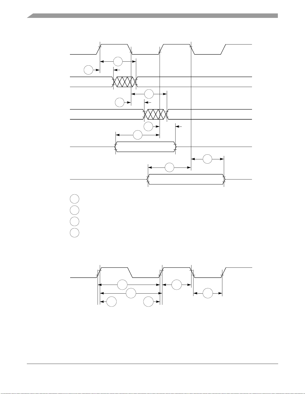
Figure 10 provides normal case t iming for in put data. It also applie s to normal r ead accesses under the co ntrol of th e
user-programmable machine (UPM) in th e memory cont roller.
CLKOUT
B16
B17
TA
B18
B19
D[0:31]
Figure 10. Input Data Timing in Normal Case
MPC885/MPC880 Hardware Specifications, Rev. 3
26 Freescale Semiconduct or
Page 27
Bus Signal Timing
Figure 11 provides the ti m ing for the input data controll ed by the UPM for data beats wh er e DLT3 = 1 in the UPM
RAM words. (This is only the case where data is latched on the falling edge of CLKOUT.)
CLKOUT
TA
B20
B21
D[0:31]
Figure 11. Input Data Timing when Controlled by UPM in the Memory Controller and DLT3 = 1
Figure 12 through Figure 15 provide the timing for the external bus read controlled by various GPCM factors.
CLKOUT
TS
A[0:31]
CSx
OE
WE[0:3]
D[0:31]
B11 B12
B8
B22
B25
B28
B23
B26
B19
B18
Figure 12. External Bus Read Timing (GPCM Controlled—ACS = 00)
MPC885/MPC880 Hardware Specifications, Rev. 3
27 Freescale Semiconduct or
Page 28
Bus Signal Timing
CLKOUT
TS
A[0:31]
B11 B12
B8
B22
CSx
B25B24
OE
D[0:31]
B23
B26
B19B18
Figure 13. External Bus Read Timing (GPCM Controlled—TRLX = 0, ACS = 10)
CLKOUT
B11 B12
TS
B22B8
A[0:31]
B22 B23
CSx
B24 B25 B26
OE
B19B18
D[0:31]
Figure 14. External Bus Read Timing (GPCM Controlled—TRLX = 0, ACS = 11)
MPC885/MPC880 Hardware Specifications, Rev. 3
28 Freescale Semiconduct or
Page 29

Bus Signal Timing
CLKOUT
TS
A[0:31]
B11 B12
B8
B23
B26
CSx
OE
D[0:31]
B22
B27
B27
B22 B22 B19B18
Figure 15. External Bus Read Timing (GPCM Controlled—TRLX = 1, ACS = 10, ACS = 11)
MPC885/MPC880 Hardware Specifications, Rev. 3
29 Freescale Semiconduct or
Page 30

Bus Signal Timing
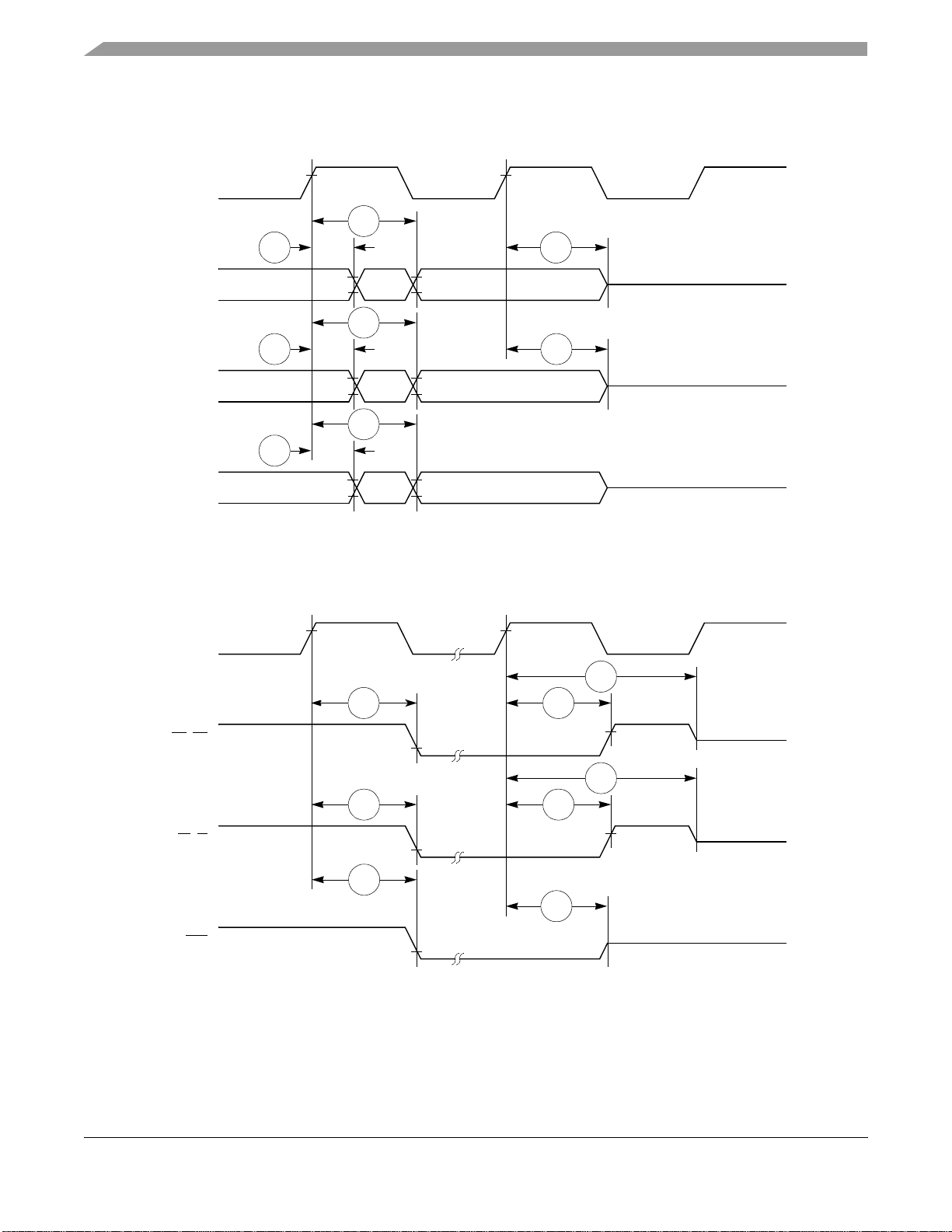
Figure 16 through Figure 18 provide the timing for the external bus write controlled by various GPCM factors.
CLKOUT
TS
A[0:31]
CSx
WE[0:3]
OE
D[0:31]
B11
B8
B22 B23
B26
B12
B8 B9
B30
B28B25
B29
B29
Figure 16. External Bus Write Timing (GPCM Controlled—TRLX = 0, CSNT = 0)
MPC885/MPC880 Hardware Specifications, Rev. 3
30 Freescale Semiconduct or
Page 31

Bus Signal Timing
CLKOUT
TS
A[0:31]
CSx
WE[0:3]
OE
D[0:31]
B11
B8
B22
B26
B8
B12
B28 B28
B25
B28B9B28
B30 B30
B23
B29 B29
B29 B29f
Figure 17. External Bus Write Timing (GPCM Controlled—TRLX = 0, CSNT = 1)
MPC885/MPC880 Hardware Specifications, Rev. 3
31 Freescale Semiconduct or
Page 32

Bus Signal Timing
CLKOUT
TS
B12B11
B8
A[0:31]
B28 B28
CSx
B25 B29 B29i
WE[0:3]
B26 B29 B29
OE
B28 B28 B9B8
D[0:31]
B30B30
B29
Figure 18. External Bus Write Timing (GPCM Controlled—TRLX = 1, CSNT = 1)
B23B22
MPC885/MPC880 Hardware Specifications, Rev. 3
32 Freescale Semiconduct or
Page 33

Bus Signal Timing
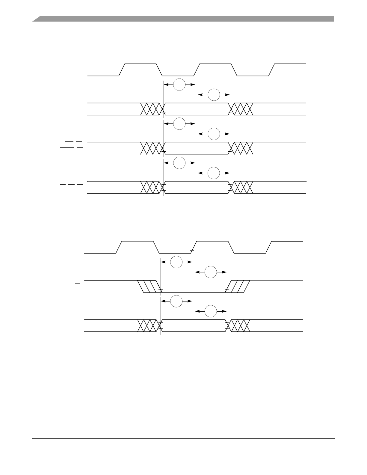
Figure 19 provides the timing for the external bus controlled by the UPM.
CLKOUT
B8
A[0:31]
B31
B31
B31
CSx
B34
B34
B34
B32 B32
B32
B31
B32
B31
B32
BS_A
[0:3],
[0:3]
BS_B
GPL_A[0:5],
[0:5]
GPL_B
B36
B35
B35
B35
B33
B33
Figure 19. External Bus Timing (UPM-Controlled Signals)
MPC885/MPC880 Hardware Specifications, Rev. 3
33 Freescale Semiconduct or
Page 34

Bus Signal Timing
Figure 20 provides the timing for the asynchronous asserted UPWAIT signal controlled by the UPM.
CLKOUT
B37
UPWAIT
B38
CSx
BS_A[0:3],
BS_B
[0:3]
GPL_A[0:5],
[0:5]
GPL_B
Figure 20. Asynchronous UPWAIT Asserted Detection in UPM-Handled Cycles Timing
Figure 21 provides the timing for the asynchronous negated UPWAIT signal controlled by the UPM.
CLKOUT
B37
UPWAIT
B38
CSx
BS_A[0:3],
[0:3]
BS_B
GPL_A
[0:5],
[0:5]
GPL_B
Figure 21. Asynchronous UPWAIT Negated Detection in UPM-Handled Cycles Timing
MPC885/MPC880 Hardware Specifications, Rev. 3
34 Freescale Semiconduct or
Page 35

Bus Signal Timing
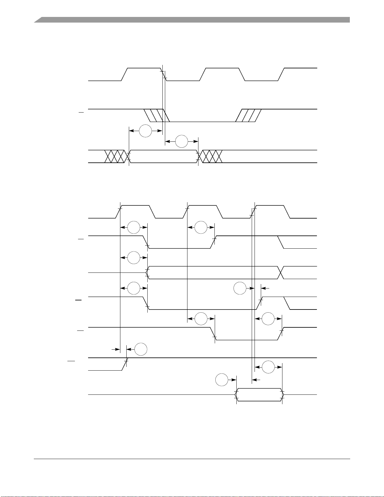
Figure 22 provides the timing for the synchronous external master access controlled by the GPCM.
CLKOUT
B41 B42
TS
B40
A[0:31],
TSIZ[0:1],
, BURST
R/W
B22
CSx
Figure 22. Synchronous External Master Access Timing (GPCM Handled—ACS = 00)
Figure 23 provides the timing for the asynchronous external master memory access controlled by the GPCM.
CLKOUT
B39
AS
B40
A[0:31],
TSIZ[0:1],
R/W
B22
CSx
Figure 23. Asynchronous External Master Memory Access Timing (GPCM Controlled—ACS = 00)
Figure 24 provides the timing for the asynchronous external master control signals negation.
AS
B43
CSx, WE[0:3],
OE, GPLx,
[0:3]
BS
Figure 24. Asynchronous External Master—Control Signals Negation Timing
MPC885/MPC880 Hardware Specifications, Rev. 3
35 Freescale Semiconduct or
Page 36

Bus Signal Timing
Table 10 provides the interrupt timing for the MPC885/880.
Table 10. Interrupt Timing
Num Characteristic
I39 IRQ
I40 IRQx hold time after CLKOUT 2.00 ns
I41 IRQx pulse width low 3.00 ns
I42 IRQx pulse width high 3.00 ns
I43 IRQx edge-to-edge time 4 × T
1
The I39 and I40 tim ing s des cri be the tes tin g c on diti on s u nde r w hi ch the IRQ lines are tested when being defined as
level sensitive. The IRQ
to the CLKOUT.
The I41, I42, and I43 timings are specified to allow correct functioning of the IRQ lines detection circuitry and have
no direct relation with the total system interrupt latency that the MPC885/880 is able to support.
x valid to CLKOUT rising edge (setup time) 6.00 ns
lines are synchronized interna lly and do no t have to be assert ed or nega ted with refe rence
1
All Frequencies
Min Max
CLOCKOUT
Figure 25 provides the interrupt detection timing for the external level-sensitive lines.
CLKOUT
I39
I40
Unit
—
x
IRQ
Figure 25. Interrupt Detection Timing for External Level Sensitive Lines
Figure 26 provides t he interrupt d etection timing for the ex ternal edge-s ensitive lines.
CLKOUT
I41 I42
IRQx
I43
I43
Figure 26. Interrupt Detection Timing for External Edge Sensitive Lines
MPC885/MPC880 Hardware Specifications, Rev. 3
36 Freescale Semiconduct or
Page 37

Bus Signal Timing
Table 11 shows the PCMCIA timing for the MPC885/880.
Table 11. PCMCIA Timing
33 MHz 40 MHz 66 MHz 80 MHz
Num Characteristic
Min Max Min Max Min Max Min Max
Unit
A(0:31), REG
strobe asserted
P44
valid to PCMCIA
(MIN = 0.75 × B1 – 2.00)
A(0:31), REG valid to ALE
P45
negation
1
(MIN = 1.00 × B1 – 2.00)
CLKOUT to REG valid
P46
(MAX = 0.25 × B1 + 8.00)
CLKOUT to REG
P47
(MIN = 0.25 – B1 + 1.00)
CLKOUT to CE1
P48
(MAX = 0.25 × B1 + 8.00)
CLKOUT to CE1
P49
(MAX = 0.25 × B1 + 8.00)
CLKOUT to PCOE
P50
, IOWR assert time
PCWE
(MAX = 0.00 × B1 + 11.00)
CLKOUT to PCOE
P51
, IOWR negate time
PCWE
(MAX = 0.00 × B1 + 11.00)
CLKOUT to ALE assert time
P52
(MAX = 0.25 × B1 + 6.30)
1
invalid
, CE2 asserted
, CE2 negated
, IORD,
, IORD,
20.70 — 16.70 — 9.40 — 7.40 — ns
28.30 — 23.00 — 13.20 — 10.50 — ns
7.60 15.60 6.30 14.30 3.80 11.80 3.13 11.13 ns
8.60 — 7.30 — 4.80 — 4.13 — ns
7.60 15.60 6.30 14.30 3.80 11.80 3.13 11.13 ns
7.60 15.60 6.30 14.30 3.80 11.80 3.13 11.13 ns
— 11.00 — 11.00 — 11.00 — 11.00 ns
2.00 11.00 2.00 11.00 2.00 11.00 2.00 11.00 ns
7.60 13.80 6.30 12.50 3.80 10.00 3.13 9.40 ns
CLKOUT to ALE negate time
P53
(MAX = 0.25 × B1 + 8.00)
, IOWR negated to
P54
PCWE
D(0:31) invalid
1
— 15.60 — 14.30 — 11.80 — 11.13 ns
5.60 — 4.30 — 1.80 — 1.13 — ns
(MIN = 0.25 × B1 – 2.00)
WAITA and WAITB valid to
P55
CLKOUT rising edge
1
8.00 — 8.00 — 8.00 — 8.00 — ns
(MIN = 0.00 × B1 + 8.00)
CLKOUT rising edge to WAITA
P56
and WAITB
invalid
1
2.00 — 2.00 — 2.00 — 2.00 — ns
(MIN = 0.00 × B1 + 2.00)
1
PSST = 1. Otherwise add PSST times cycle time.
PSHT = 0. Otherwise add PSHT times cycle time.
These synchronous tim ings define when the WAITx
current cycle. The W AITx
assertion will be ef fective only if it is dete cted 2 cycles before th e PSL timer expiration. See
signals are detected in or der to freez e (or relie ve) the PCMCIA
Chapter 16, “PCMCIA Interface,” in the MPC885 PowerQUICC Family User’s Manual.
MPC885/MPC880 Hardware Specifications, Rev. 3
37 Freescale Semiconduct or
Page 38

Bus Signal Timing
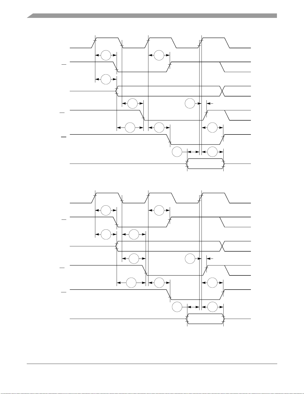
Figure 27 provides the PCMCIA access cycle timing for the external bus read.
CLKOUT
TS
P44
A[0:31]
REG
CE1/CE2
PCOE, IORD
ALE
D[0:31]
P46 P45
P48 P49
P53P52 P52
P47
P51P50
Figure 27. PCMCIA Access Cycles Timing External Bus Read
B19B18
MPC885/MPC880 Hardware Specifications, Rev. 3
38 Freescale Semiconduct or
Page 39

Bus Signal Timing
Figure 28 provides t he PCMCIA access cycle timing for the external bus write.
CLKOUT
TS
P44
A[0:31]
P46 P45
REG
P48 P49
CE1/CE2
PCWE, IOWR
P53P52 P52
ALE
D[0:31]
Figure 28. PCMCIA Access Cycles Timing External Bus Write
Figure 29 provides the PCMCIA WAIT signals detection timing.
P47
P51P50
P54
B9B8
CLKOUT
P55
P56
WAITx
Figure 29. PCMCIA WAIT Signals Detection Timing
MPC885/MPC880 Hardware Specifications, Rev. 3
39 Freescale Semiconduct or
Page 40

Bus Signal Timing
Table 12 shows the PCMCIA port timing for the MPC885/880.
Table 12. PCMCIA Port Timing
33 MHz 40 MHz 66 MHz 80 MHz
Num Characteristic
Min Max Min Max Min Max Min Max
Unit
CLKOUT to OPx valid
P57
(MAX = 0.00 × B1 + 19.00)
HRESET
P58
(MIN = 0.75 × B1 + 3.00)
IP_Xx valid to CLKOUT rising edge
P59
(MIN = 0.00 × B1 + 5.00)
CLKOUT rising edge to IP_Xx invalid
P60
(MIN = 0.00 × B1 + 1.00)
1
OP2 and OP3 only.
negated to OPx drive 1
— 19.00 — 19.00 — 19.00 — 19.00 ns
25.70 — 21.70 — 14.40 — 12.40 — ns
5.00 — 5.00 — 5.00 — 5.00 — ns
1.00 — 1.00 — 1.00 — 1.00 — ns
Figure 30 provides the PCMCIA output port timing for the MPC885/880.
CLKOUT
P57
Output
Signals
HRESET
P58
OP2, OP3
Figure 30. PCMCIA Output Port Timing
Figure 31 provides the PCMCIA input port timing for the MPC885/880.
CLKOUT
P59
P60
Input
Signals
Figure 31. PCMCIA Input Port Timing
MPC885/MPC880 Hardware Specifications, Rev. 3
40 Freescale Semiconduct or
Page 41

Bus Signal Timing
Table 13 shows the debug port timing for the MPC885/880.
Table 13. Debug Port Timing
Num Characteristic
All Frequencies
Unit
Min Max
DSCK cycle time 3 × T
D61
DSCK clock pulse width 1.25 × T
D62
D63 DSCK rise and fall times 0.00 3.00 ns
D64 DSDI input data setup time 8.00 ns
D65 DSDI data hold time 5.00 ns
D66 DSCK low to DSDO data valid 0.00 15.00 ns
D67 DSCK low to DSDO invalid 0.00 2.00 ns
CLOCKO
UT
CLO
CKOUT
Figure 32 provides the input timing for the debug port clock.
DSCK
D61
D61
D63
Figure 32. Debug Port Clock Input Timing
D62
D62
D63
-
-
Figure 33 provides the timing for the debug port.
DSCK
DSDI
D66
DSDO
Figure 33. Debug Port Timings
MPC885/MPC880 Hardware Specifications, Rev. 3
D64
D65
D67
41 Freescale Semiconduct or
Page 42

Bus Signal Timing
Table 14 shows the reset timing for the MPC885/880.
T a b l e 14. Re se t Timing
33 MHz 40 MHz 66 MHz 80 MHz
Num Characteristic
Min Max Min Max Min Max Min Max
Unit
CLKOUT to HRESET
impedance
R69
(MAX = 0.00 × B1 + 20.00)
CLKOUT to SRESET high
R70
impedance
(MAX = 0.00 × B1 + 20.00)
RSTCONF pulse width
R71
(MIN = 17.00 × B1)
R72 — —————————
Configuration data to HRESET
R73
rising edge setup time
(MIN = 15.00 × B1 + 50.00)
Configuration data to RSTCONF
rising edge setup time
R74
(MIN = 0.00 × B1 + 350.00)
Configuration data hold time after
R75
RSTCONF
(MIN = 0.00 × B1 + 0.00)
Configuration data hold time after
R76
HRESET
(MIN = 0.00 × B1 + 0.00)
HRESET
R77
asserted t o data out drive
(MAX = 0.00 × B1 + 25.00)
negation
negation
and RSTCONF
high
— 20.00 — 20.00 — 20.00 — 20.00 ns
— 20.00 — 20.00 — 20.00 — 20.00 ns
515.20 — 425.00 — 257.60 — 212.50 — ns
504.50 — 425.00 — 277.30 — 237.50 — ns
350.00 — 350.00 — 350.00 — 350.00 — ns
0.00 — 0.00 — 0.00 — 0.00 — ns
0.00 — 0.00 — 0.00 — 0.00 — ns
— 25.00 — 25.00 — 25.00 — 25.00 ns
RSTCONF
high impedance
R78
(MAX = 0.00 × B1 + 25.00)
CLKOUT of last rising edge
before chip three-states
R79
HRESET to data out high
impedance
(MAX = 0.00 × B1 + 25.00)
DSDI, DSCK setup
R80
(MIN = 3.00 × B1)
DSDI, DSCK hold time
R81
(MIN = 0.00 × B1 + 0.00)
SRESET
rising edge for DSDI and DSCK
R82
sample (MIN = 8.00 × B1)
42 Freescale Semiconduct or
negated to data out
negated to CLKOUT
MPC885/MPC880 Hardware Specifications, Rev. 3
— 25.00 — 25.00 — 25.00 — 25.00 ns
— 25.00 — 25.00 — 25.00 — 25.00 ns
90.90 — 75.00 — 45.50 — 37.50 — ns
0.00 — 0.00 — 0.00 — 0.00 — ns
242.40 — 200.00 — 121.20 — 100.00 — ns
Page 43

Bus Signal Timing
Figure 34 shows the reset timing for the data bus configuration.
HRESET
R71
R76
RSTCONF
R73
R74
D[0:31] (IN)
R75
Figure 34. Reset Timing—Configuration from Data Bus
Figure 35 provides the reset timing for the data bus weak drive during configuration.
CLKOUT
HRESET
RSTCONF
D[0:31] (OUT)
(Weak)
R69
R79
R77 R78
Figure 35. Reset Timing—Data Bus Weak Drive During Configuration
MPC885/MPC880 Hardware Specifications, Rev. 3
43 Freescale Semiconduct or
Page 44

IEEE 1149.1 Electrical Specifications
Figure 36 provides the reset timing for the debug port configuration.
CLKOUT
R70
R82
SRESET
R80R80
R81
DSCK, DSDI
R81
Figure 36. Reset Timing—Debug Port Configuration
11 IEEE 1149.1 Electrical Specifications
Table 15 provides the JTAG timings for the MPC885/880 shown in Figure 37 to Figure 40.
Table 15. JTAG Timing
All
Num Characteristic
J82 TCK cycle time 100.00 — ns
J83 TCK clock pulse width measured at 1.5 V 40.00 — ns
J84 TCK rise and fall times 0.00 10.00 ns
J85 TMS, TDI data setup time 5.00 — ns
J86 TMS, TDI data hold time 25.00 — ns
J87 TCK low to TDO data valid — 27.00 ns
J88 TCK low to TDO data invalid 0.00 — ns
J89 TCK low to TDO high impedance — 20.00 ns
J90 TRST
J91 TRST setup time to TCK low 40.00 — ns
J92 TCK falling edge to output valid — 50.00 ns
J93 TCK falling edge to output valid out of high impedance — 50.00 ns
J94 TCK falling edge to output high impedance — 50.00 ns
J95 Boundary scan input valid to TCK rising edge 50.00 — ns
assert time 100.00 — ns
Frequencies
Min Max
Unit
J96 TCK rising edge to boundary scan input invalid 50.00 — ns
MPC885/MPC880 Hardware Specifications, Rev. 3
44 Freescale Semiconduct or
Page 45

IEEE 1149.1 Electrical Specifications
TCK
TCK
TMS, TDI
J82 J83
J82 J83
J84 J84
Figure 37. JTAG Test Clock Input Timing
J85
J86
J87
J88 J89
TDO
TCK
TRST
Figure 38. JTAG Test Access Port Timing Diagram
J91
J90
Figure 39. JTAG TRST
Timing Diagram
MPC885/MPC880 Hardware Specifications, Rev. 3
45 Freescale Semiconduct or
Page 46

CPM Electrical Characteristics
TCK
J92 J94
Output
Signals
J93
Output
Signals
J95 J96
Output
Signals
Figure 40. Boundary Scan (JTAG) Timing Diagram
12 CPM Electrical Characteristics
This section pr ovi des t he AC and DC electrical specifications for the communicat ions processor module (CPM ) of
the MPC885/880.
12.1 PIP/PIO AC Electrical Specifications
Table 16 provides the PIP/PIO AC timings as shown in Figure 41 to Figure 45.
Table 16. PIP/PIO Timing
Num Characteristic
21 Data-in setup time to STBI low 0 — ns
22 Data-In hold time to STBI high 0 — clk
23 STBI pulse width 1.5 — clk
24 STBO pulse width 1 clk – 5 ns — n s
25 Data-out setup time to STBO low 2 — clk
26 Data-out hold time from STBO high 5 — clk
27 STBI low to STBO low (Rx interlock) — 4.5 clk
28 STBI low to STBO high (Tx interlock) 2 — clk
29 Data-in setup time to clock high 15 — ns
30 Data-in hold time from clock high 7.5 — ns
31 Clock low to data-out valid (CPU writes data, control, or direction) — 25 ns
All Frequencies
Unit
Min Max
MPC885/MPC880 Hardware Specifications, Rev. 3
46 Freescale Semiconduct or
Page 47

CPM Electrical Characteristics
DA TA-IN
STBI
STBO
DA TA-OUT
STBO
(Output)
21
23
27
24
22
Figure 41. PIP Rx (Interlock Mode) Timing Diagram
25
24
28
23
26
STBI
(Input)
DA TA-IN
STBI
(Input)
STBO
(Output)
Figure 42. PIP Tx (Interlock Mode) Timing Diagram
2221
23
24
Figure 43. PIP Rx (Pulse Mode) Timing Diagram
MPC885/MPC880 Hardware Specifications, Rev. 3
47 Freescale Semiconduct or
Page 48

CPM Electrical Characteristics
DA T A-OUT
STBO
(Output)
STBI
(Input)
CLKO
2625
24
23
Figure 44. PIP TX (Pulse Mode) Timing Diagram
29
30
DA TA-IN
31
DA T A-OUT
Figure 45. Parallel I/O Data-In/Data-Out Timing Diagram
12.2 Port C Interrupt AC Electrical Specifications
Table 17 provides the timings for port C interrupts.
Table 17. Port C Interrupt Timing
Num Characteristic
35 Port C interrupt pulse width low (edge-triggered mode) 55 — ns
36 Port C interrupt minimum time between active edges 55 — ns
33.34 MHz
Unit
Min Max
MPC885/MPC880 Hardware Specifications, Rev. 3
48 Freescale Semiconduct or
Page 49

CPM Electrical Characteristics
Figure 46 shows the port C interrupt detection timing.
36
Port C
(Input)
35
Figure 46. Port C Interrupt Detection Timing
12.3 IDMA Controller AC Electrical Specifications
Table 18 provides the IDMA controller timings as shown in Figure 47 to Figure 50.
Table 18. IDMA Controller Timing
Num Characteristic
40 DREQ setup time to clock high 7 — ns
41 DREQ hold time from clock high
1
All Frequencies
Unit
Min Max
TBD — ns
42 SDACK assertion delay from clock high — 12 ns
43 SDACK negation delay from clock low — 12 ns
44 SDACK negation delay from TA low — 20 ns
45 SDACK negation delay from clock high — 15 ns
46 TA assertion to falling edge of the clock setup time (applies to external TA)7 — ns
1
Applies to high-to-low mode (EDM=1)
CLKO
(Output)
41
40
DREQ
(Input)
Figure 47. IDMA External Requests Timing Diagram
MPC885/MPC880 Hardware Specifications, Rev. 3
49 Freescale Semiconduct or
Page 50

CPM Electrical Characteristics
CLKO
(Output)
TS
(Output)
R/W
(Output)
42
DA T A
TA
(Input)
SDACK
43
46
Figure 48. SDACK Timing Diagram—Peripheral Write, Externally-Generate d TA
CLKO
(Output)
TS
(Output)
R/W
(Output)
42 44
DA T A
TA
(Output)
SDACK
Figure 49. SDACK Timing Diagram—Peripheral Write, Internally-Generated TA
MPC885/MPC880 Hardware Specifications, Rev. 3
50 Freescale Semiconduct or
Page 51

CPM Electrical Characteristics
CLKO
(Output)
TS
(Output)
R/W
(Output)
DA T A
TA
(Output)
SDACK
42 45
Figure 50. SDACK Timing Diagram—Peripheral Read, Internally-Generated TA
12.4 Baud Rate Generator AC Electrical Specifications
Table 19 provides the baud rate generator timings as shown in Figure 51.
Table 19. Baud Rate Generator Timing
All Frequencies
Num Characteristic
Min Max
50 BRGO rise and fall time — 10 ns
51 BRGO duty cycle 40 60 %
52 BRGO cycle 40 — ns
50
BRGOX
51
52
50
51
Unit
Figure 51. Baud Rate Generator Timing Diagram
MPC885/MPC880 Hardware Specifications, Rev. 3
51 Freescale Semiconduct or
Page 52

CPM Electrical Characteristics
12.5 Timer AC Electrical Specifications
Table 20 provides the general-purpose timer timings as shown in Figure 52.
Num Characteristic
61 TIN/TGATE rise and fall time 10 — ns
62 TIN/TGATE low time 1 — clk
63 TIN/TGATE high time 2 — clk
64 TIN/TGATE cycle time 3 — clk
65 CLKO low to TOUT valid 3 25 ns
CLKO
Table 20. Timer Ti ming
60
All Frequencies
Unit
Min Max
626361
TIN/TGATE
(Input)
61
65
TOUT
(Output)
64
Figure 52. CPM General-Purpose Timers Timing Diagram
12.6 Serial Interface AC Electrical Specifications
Table 21 provides the serial interface timings as shown in Figure 53 to Figure 57.
Num Characteristic
70 L1RCLK, L1TCLK frequency (DSC = 0)
71 L1RCLK, L1TCLK width low (DSC = 0)
71a L1RCLK, L1TCLK width high (D SC = 0)
Table 21. SI Timing
All Frequencies
Min Max
1, 2
— SYNCCLK
2
3
P + 10 — ns
P + 10 — ns
Unit
MHz
/2.5
72 L1TXD, L1ST(1–4), L1RQ, L1CLKO rise/fall time — 15.00 ns
73 L1RSYNC, L1TSYNC valid to L1CLK edge (SYNC setup time) 20.00 — ns
74 L1CLK edge to L1RSYNC, L1TSYNC, invalid (SYNC hold time) 35.00 — ns
MPC885/MPC880 Hardware Specifications, Rev. 3
52 Freescale Semiconduct or
Page 53

CPM Electrical Characteristics
Table 21. SI Timing (continued)
All Frequencies
Num Characteristic
Min Max
75 L1RSYNC, L1TSYNC rise/fall time — 15.00 ns
76 L1RXD valid to L1CLK edge (L1RXD setup time) 17.00 — ns
77 L1CLK edge to L1RXD invalid (L1RXD hold time) 13.00 — ns
78 L1CLK edge to L1ST(1–4) valid
78A L1SYNC valid to L1ST(1–4) valid 10.00 45.00 ns
79 L1CLK edge to L1ST(1–4) invalid 10.00 45.00 ns
80 L1CLK edge to L1TXD valid 10.00 55.00 ns
80A L1TSYNC valid to L1TXD valid
81 L1CLK edge to L1TXD high impedance 0.00 42.00 ns
4
4
10.00 45.00 ns
10.00 55.00 ns
Unit
82 L1RCLK, L1TCLK frequency (DSC =1) — 16.00 or
MHz
SYNCCLK
/2
83 L1RCLK, L1TCLK width low (DSC =1) P + 10 — ns
83a L1RCLK, L1TCLK width high (D SC = 1)
3
P + 10 — ns
84 L1CLK edge to L1CLKO valid (DSC = 1) — 30.00 ns
85 L1RQ valid before falling edge of L1TSYNC
86 L1GR setup time
2
4
1.00 — L1TCLK
42.00 — ns
87 L1GR hold time 42.00 — ns
88 L1CLK edge to L1SYNC valid (FSD = 00) CNT = 0000, BYT = 0,
—0.00ns
DSC = 0)
1
The ratio SyncCLK/L1RCLK must be greater than 2.5/1.
2
These specs are valid for IDL mode only.
3
Where P = 1/CLKOUT. Thus for a 25-MHz CLKO1 rate, P = 40 ns.
4
These strobes and TxD on the first bit of the frame become valid after L1CLK edge or L1SYNC, whichever comes later.
MPC885/MPC880 Hardware Specifications, Rev. 3
53 Freescale Semiconduct or
Page 54

CPM Electrical Characteristics
(
(
L1RCLK
FE=0, CE=0)
(Input)
71
L1RCLK
FE=1, CE=1)
(Input)
L1RSYNC
(Input)
73
70 71a
72
RFSD=1
75
74 77
L1RXD
(Input)
76
L1ST(4-1)
(Output)
BIT0
78
79
Figure 53. SI Receive Timing Diagram with Normal Clocking (DSC = 0)
MPC885/MPC880 Hardware Specifications, Rev. 3
54 Freescale Semiconduct or
Page 55

CPM Electrical Characteristics
(
(
L1RCLK
FE=1, CE=1)
(Input)
82
L1RCLK
FE=0, CE=0)
(Input)
L1RSYNC
(Input)
72
RFSD=1
75
73
74 77
83a
L1RXD
(Input)
76
L1ST(4-1)
(Output)
L1CLKO
(Output)
BIT0
84
78
79
Figure 54. SI Receive Timing with Double-Speed Clocking (DSC = 1)
MPC885/MPC880 Hardware Specifications, Rev. 3
55 Freescale Semiconduct or
Page 56

CPM Electrical Characteristics
(
(
L1TCLK
FE=0, CE=0)
(Input)
71 70
L1TCLK
FE=1, CE=1)
(Input)
73
L1TSYNC
(Input)
80a
72
TFSD=0
75
74
81
L1TXD
(Output)
L1ST(4-1)
(Output)
BIT0
80
78
79
Figure 55. SI Transmit Timing Diagram (DSC = 0)
MPC885/MPC880 Hardware Specifications, Rev. 3
56 Freescale Semiconduct or
Page 57

CPM Electrical Characteristics
(
(
L1RCLK
FE=0, CE=0)
(Input)
L1RCLK
FE=1, CE=1)
(Input)
L1RSYNC
(Input)
73
75
74
72
82
TFSD=0
83a
81
L1TXD
(Output)
L1ST(4-1)
(Output)
L1CLKO
(Output)
BIT0
80
84
78a
78
79
Figure 56. SI Transmit Timing with Double Speed Clocking (DSC = 1)
MPC885/MPC880 Hardware Specifications, Rev. 3
57 Freescale Semiconduct or
Page 58

CPM Electrical Characteristics
81
78
87
72
71
71
12345678910 11 12 13 14 15 16 17 18 19 20
73
74
76
B17 B16 B15 B14 B13 B12 B11 B10 D1 A B27 B26 B25 B24 B23 B22 B21 B20 D2 M
B17 B16 B14 B13 B12 B11 B10 D1 A B27 B26 B25 B24 B23 B22 B21 B20 D2 MB15
85
86
77
80
(Input)
L1RCLK
(Input)
L1RSYNC
L1TXD
(Output)
(Input)
L1RXD
(Output)
L1ST(4-1)
L1RQ
(Output)
L1GR
(Input)
Figure 57. IDL Timing
MPC885/MPC880 Hardware Specifications, Rev. 3
58 Freescale Semiconduct or
Page 59

CPM Electrical Characteristics
12.7 SCC in NMSI Mode Electrical Specifications
Table 22 provides the NMSI external clock timing.
Table 22. NMSI External Clock Timing
All Frequencies
Num Characteristic
Min Max
100 RCLK1 and TCLK1 width high
101 RCLK1 and TCLK1 width low 1/SYNCCLK + 5 — ns
102 RCLK1 and TCLK1 rise/fall time — 15.00 ns
103 TXD1 active delay (from TCLK1 falling edge) 0.00 50.00 ns
104 RTS1 active/inactive delay (from TCLK1 falling edge) 0.00 50.00 ns
105 CTS1 setup time to TCLK1 rising edge 5.00 — ns
106 RXD1 setup time to RCLK1 rising edge 5.00 — ns
107 RXD1 hold time from RCLK1 rising edge
108 CD1 setup time to RCLK1 rising edge 5.00 — ns
1
The ratios SyncCLK/RCLK1 and SyncCLK/TCLK1 must be greater than or equal to 2.25/1.
2
Also applies to CD and CTS hold time when they are used as external sync signals.
1
2
1/SYNCCLK — ns
5.00 — ns
Unit
Table 23 provides the NMSI internal clock timing.
Table 23. NMSI Internal Clo ck Timing
All Frequencies
Num Characteristic
Min Max
100 RCLK1 and TCLK1 frequency
102 RCLK1 and TCLK1 rise/fall time — — ns
103 TXD1 active delay (from TCLK1 falling edge) 0.00 30.00 ns
104 RTS1 active/inactive delay (from TCLK1 falling edge) 0.00 30.00 ns
105 CTS1 setup time to TCLK1 rising edge 40.00 — ns
106 RXD1 setup time to RCLK1 rising edge 40.00 — ns
107 RXD1 hold time from RCLK1 rising edge
108 CD1 setup time to RCLK1 rising edge 40.00 — ns
1
The ratios SyncCLK/RCLK1 and SyncCLK/TCLK1 must be greater than or equal to 3/1.
2
Also applies to CD and CTS hold time when they are used as external sync signals
1
2
0.00 SYNCCLK/3 MHz
0.00 — ns
Unit
MPC885/MPC880 Hardware Specifications, Rev. 3
59 Freescale Semiconduct or
Page 60

CPM Electrical Characteristics
Figure 58 through Figure 60 show the NMSI timings.
RCLK1
RxD1
(Input)
CD1
(Input)
CD1
(SYNC Input)
TCLK1
106
102
102
102 101
100
107
Figure 58. SCC NMSI Receive Timing Diagram
102 101
100
108
107
TxD1
(Output)
RTS1
(Output)
CTS1
(Input)
CTS1
(SYNC Input)
103
105
104
Figure 59. SCC NMSI Transmit Timing Diagram
104
107
MPC885/MPC880 Hardware Specifications, Rev. 3
60 Freescale Semiconduct or
Page 61

CPM Electrical Characteristics
TCLK1
102
TxD1
(Output)
RTS1
(Output)
CTS1
(Echo Input)
102 101
100
103
104
105
Figure 60. HDLC Bus Timing Diagram
12.8 Ethernet Electrical Specifications
Table 24 provides the Ethernet timings as shown in Figure 61 to Figure 63.
Table 24. Ethernet Timing
104107
All Frequencies
Num Characteristic
Min Max
120 CLSN width high 40 — ns
121 RCLK1 rise/fall time — 15 ns
122 RCLK1 width low 40 — ns
123 RCLK1 clock period
124 RXD1 setup time 20 — ns
125 RXD1 hold time 5 — ns
126 RENA active delay (from RCLK1 rising edge of the last data bit) 10 — ns
127 RENA width low 10 0 — ns
128 TCLK1 rise/fall time — 15 ns
129 TCLK1 width low 40 — ns
130 TCLK1 clock period
131 TXD1 active delay (from TCLK1 rising edge) — 50 ns
132 TXD1 inactive delay (from TCLK1 rising edge) 6.5 50 ns
133 TENA active delay (from TCLK1 rising edge) 10 50 ns
1
1
80 120 ns
99 101 ns
Unit
MPC885/MPC880 Hardware Specifications, Rev. 3
61 Freescale Semiconduct or
Page 62

CPM Electrical Characteristics
Table 24. Ethernet Timing (continued)
All Frequencies
Num Characteristic
Min Max
134 TENA inactive delay (from TCLK1 rising edge) 10 50 ns
138 CLKO1 low to SDACK asserted
139 CLKO1 low to SDACK negated
1
The ratios SyncCLK/RCLK1 and SyncCLK/TCLK1 must be greater than or equal to 2/1.
2
SDACK is asserted whenever the SDMA writes the incoming frame DA into memory.
2
2
—20ns
—20ns
CLSN(CTS1)
(Input)
120
Figure 61. Ethernet Collision Timing Diagram
RCLK1
Unit
RxD1
(Input)
RENA(CD1)
(Input)
121
121
124 123
125
126
Figure 62. Ethernet Receive Timing Diagram
Last Bit
127
MPC885/MPC880 Hardware Specifications, Rev. 3
62 Freescale Semiconduct or
Page 63

CPM Electrical Characteristics
TCLK1
TxD1
(Output)
TENA(RTS1)
(Input)
RENA(CD1)
(Input)
(NOTE 2)
128
131 121
133 134
NOTES:
Transmit clock invert (TCI) bit in GSMR is set.
1.
If RENA is negated before TENA or RENA is not asserted at all during transmit, then the
2.
CSL bit is set in the buffer descriptor at the end of the frame transmission.
128
129
132
Figure 63. Ethernet Transmit Timing Diagram
12.9 SMC Transparent AC Electrical Specifications
Table 25 provides the SMC transparent timings as shown in Figure 64.
T able 25. SMC Transp arent Timing
All Frequencies
Num Characteristic
Min Max
150 SMCLK clock period
151 SMCLK width low 50 — ns
151A SMCLK width high 50 — ns
152 SMCLK rise/fall time — 15 ns
153 SMTXD active delay (from SMCLK falling edge) 10 50 ns
154 SMRXD/SMSYNC setup time 20 — ns
155 RXD1/SMSYNC hold time 5 — ns
1
SyncCLK must be at least twice as fast as SMCLK.
1
100 — ns
Unit
MPC885/MPC880 Hardware Specifications, Rev. 3
63 Freescale Semiconduct or
Page 64

CPM Electrical Characteristics
SMCLK
152
SMTXD
(Output)
SMSYNC
SMRXD
(Input)
NOTE:
This delay is equal to an integer number of charac ter-length clocks.1.
152 151
NOTE
154 153
155
154
155
151
150
Figure 64. SMC Transparent Timing Diagram
12.10SPI Master AC Electrical Specifications
Table 26 provides the SPI master timings as shown in Figure 65 and Figure 66.
Table 26. SPI Master Timing
All Frequencies
Num Characteristic
Min Max
160 MASTER cycle time 4 1024 t
161 MASTER clock (SCK) high or low time 2 512 t
162 MASTER data setup time (inputs) 15 — ns
163 Master data hold time (inputs) 0 — ns
164 Master data valid (after SCK edge) — 10 ns
165 Master data hold time (outputs) 0 — ns
166 Rise time output — 15 ns
167 Fall time output — 15 ns
Unit
cyc
cyc
MPC885/MPC880 Hardware Specifications, Rev. 3
64 Freescale Semiconduct or
Page 65

CPM Electrical Characteristics
SPICLK
(CI=0)
(Output)
161 160
SPICLK
(CI=1)
(Output)
163
162
166167161
167
166
SPIMISO
(Input)
SPIMOSI
(Output)
SPICLK
(CI=0)
(Output)
SPICLK
(CI=1)
(Output)
SPIMISO
(Input)
msb Data lsb msb
165 164
167 166
msb lsb msb
Data
Figure 65. SPI Master (CP = 0) Timing Diagram
166167161
161 160
162
163
166
msb Data lsb msb
167
165 164
167 166
SPIMOSI
(Output)
msb lsb msb
Data
Figure 66. SPI Master (CP = 1) Timing Diagram
MPC885/MPC880 Hardware Specifications, Rev. 3
65 Freescale Semiconduct or
Page 66

CPM Electrical Characteristics
12.11SPI Slave AC Electrical Specifications
Table 27 provides the SPI slave timings as shown in Figure 67 and Figure 68.
Table 27. SPI Slave Timing
Num Characteristic
All Frequencies
Unit
Min Max
170 Slave cycle time 2 — t
171 Slave enable lead time 15 — ns
172 Slave enable lag time 15 — ns
173 Slave clock (SPICLK) high or low time 1 — t
174 Slave sequential transfer delay (does not require deselect) 1 — t
175 Slave data setup time (inputs) 20 — ns
176 Slave data hold time (inputs) 20 — ns
177 Slave access time — 50 ns
SPISEL
(Input)
171172
174
SPICLK
(CI=0)
(Input)
181182173
173 170
SPICLK
(CI=1)
(Input)
177 182
180
181
178
cyc
cyc
cyc
SPIMISO
(Output)
SPIMOSI
(Input)
175 179
176 182
msb lsb msb
Datamsb lsb msbUndef
181
Data
Figure 67. SPI Slave (CP = 0) Timing Diagram
MPC885/MPC880 Hardware Specifications, Rev. 3
66 Freescale Semiconduct or
Page 67

CPM Electrical Characteristics
SPISEL
(Input)
171 170
SPICLK
(CI=0)
(Input)
173
SPICLK
(CI=1)
(Input)
177 182
173
180
172
174
181182
181
178
SPIMISO
(Output)
175 179
SPIMOSI
(Input)
msb
176 182
msb lsb
Data
181
Data
lsbUndef
Figure 68. SPI Slave (CP = 1) Timing Diagram
12.12I2C AC Electrical Specifications
Table 28 provides the I2C (SCL < 100 KHz) timings.
Table 28. I2C Timing (SCL < 100 KHZ)
All Frequencies
Num Characteristic
Min Max
200 SCL clock frequency (slave) 0 100 KHz
200 SCL clock frequency (master)
202 Bus free time between transmissions 4.7 — µs
203 Low period of SCL 4.7 — µs
1
1.5 100 KHz
msb
msb
Unit
204 High period of SCL 4.0 — µs
205 Start condition setup time 4.7 — µs
206 Start condition hold time 4.0 — µs
207 Data hold time 0 — µs
208 Data setup time 250 — ns
209 SDL/SCL rise time — 1 µs
MPC885/MPC880 Hardware Specifications, Rev. 3
67 Freescale Semiconduct or
Page 68

CPM Electrical Characteristics
Table 28. I2C Timing (SCL < 100 KHZ) (continued)
All Frequencies
Num Characteristic
Min Max
210 SDL/SCL fall time — 300 ns
211 Stop condition setup time 4.7 — µs
1
SCL frequency is given by SCL = BRGCLK_frequency / ((BRG register + 3) × pre_scaler × 2).
The ratio SyncClk/(BRGCLK/pre_scaler) must be greater or equal to 4/1.
Table 29 provides the I2C (SCL > 100 KHz) timings.
2
Table 29. I
Num Characteristic Expression
200 SCL clock frequency (slave) fSCL 0 BRGCLK/48 Hz
200 SCL clock frequency (master)
202 Bus free time between transmissions — 1/(2.2 × fSCL) — s
1
C Timing (SCL > 100 KHZ)
All Frequencies
Min Max
fSCL BRGCLK/16512 BRGCLK/48 Hz
Unit
Unit
203 Low period of SCL — 1/(2.2 × fSCL) — s
204 High period of SCL — 1/(2.2 × fSCL) — s
205 Start condition setup time — 1/(2.2 × fSCL) — s
206 Start condition hold time — 1/(2.2 × fSCL) — s
207 Data hold time — 0 — s
208 Data setup time — 1 /(40 × fSCL) — s
209 SDL/SCL rise time — — 1/(10× fSCL) s
210 SDL/SCL fall time — — 1/(33 × fSCL) s
211 Stop condition setup time — 1/2(2.2 × fSCL) — s
1
SCL frequency is give n by SCL = BrgClk_freq uency / ((BRG reg ister + 3)× pre_scaler × 2).
The ratio SyncClk/(Brg_Clk/pre_scaler) must be greater or equal to 4/1.
MPC885/MPC880 Hardware Specifications, Rev. 3
68 Freescale Semiconduct or
Page 69

UTOPIA AC Electrical Specifications
Figure 69 shows the I2C bus timing.
SDA
202
205
SCL
206 209 211210
203
207
204
208
Figure 69. I2C Bus Timing Diagram
13 UTOPIA AC Electrical Specifications
Table 30, Table 31, and Table 32, show the AC electrical sp ecifications for the UTOPIA interface.
T able 30. UTOPIA Master (Muxed Mode) Electrical Specifications
Num Signal Characteristic Direction Min Max Unit
U1 UtpClk rise/fall time (internal clock option) Output 4 ns ns
Duty cycle 50 50 %
Frequency 33 MHz
U2 UTPB, SOC, RxEnb
PHREQ and PHSEL active delay in multi-PHY mode)
U3 UTPB, SOC, Rxclav and Txclav setup time Input 4 ns ns
, TxEnb, RxAddr, and TxAddr active delay (and
Output 2 ns 16 ns ns
U4 UTPB, SOC, Rxclav and Txclav hold time Input 1 ns ns
Table 31. UTOPIA Master (Split Bus Mode) Electrical Specifications
Num Signal Characteristic Direction Min Max Unit
U1 UtpClk rise/fall time (Internal clock option) Output 4 ns ns
Duty cycle 50 50 %
Frequency 33 MHz
U2 UTPB, SOC, RxEnb
(PHREQ and PHSEL active delay in multi-PHY mode)
U3 UTPB_Aux, SOC_Aux, Rxclav and Txclav setup time Input 4 ns ns
U4 UTPB_Aux, SOC_Aux, Rxclav and Txclav hold time Input 1 ns ns
, TxEnb, RxAddr and TxAddr active delay
MPC885/MPC880 Hardware Specifications, Rev. 3
Output 2 ns 16 ns ns
69 Freescale Semiconduct or
Page 70

UTOPIA AC Electrical Specifications
Table 32. UTOPIA Slave (Split Bus Mode) Electrical Specifications
Num Signal Characteristic Direction Min Max Unit
U1 UtpClk rise/fall time (external clock option) Input 4 ns ns
Duty cycle 40 60 %
Frequency 33 MHz
U2 UTPB, SOC, Rxclav and Txclav active delay Output 2 ns 16 ns ns
U3 UTPB_AUX, SOC_Aux, RxEnb
time
U4 UTPB_AUX, SOC_Aux, RxEnb
time
, TxEnb, RxAddr, and TxAddr setup
, TxEnb, RxAddr, and TxAddr hold
Figure 70 shows signal timings during UTOPIA receive operations.
U1
UtpClk
U2
PHREQn
U3 U4
3
RxClav
RxEnb
UTPB
SOC
High-Z at MPH Y
U2
2
Input 4 ns ns
Input 1 ns ns
U1
4
High-Z at MPH Y
U3
U4
3
4
Figure 70. UTOPIA Receive Timing
MPC885/MPC880 Hardware Specifications, Rev. 3
70 Freescale Semiconduct or
Page 71

USB Electrical Characteristics
YP
Figure 71 shows signal timings during UTOPIA transmit operations.
UtpClk
U2
5
PHSELn
TxClav
TxEnb
UTPB
SOC
High-Z at MPH Y High-Z at Multi -PH
U2
2
U2
5
Figure 71. UTOPIA Transmit Timing
14 USB Electrical Characteristics
This section provides the AC timings for the USB interface.
U1
1
U3 U4
3
4
U1
14.1 USB Interface AC Timing Specifications
The USB Port uses the transmit clock on SCC1. Table 33 lists th e USB interface timings.
Table 33. USB Interface AC Timing Specifications
Name Characteristic
US1 USBCLK frequency of operation
Low speed
Full speed
US4 USBCLK duty cycle (measured at 1.5 V) 45 55 %
1
USBCLK accuracy should be ±500 ppm or better. USBCLK may be stopped to conserve power.
1
All Frequencies
Min Max
6
48
Unit
MHz
MHz
15 FEC Electrical Characteristics
This section provides the AC electrical specifications for the fast Ethernet controller (FEC). Note that the timing
specifications for the MII signals are independent of system clock frequency (part speed designation). Also, MII
signals use TTL signal levels compatible with devices operating at either 5.0 V or 3.3 V.
MPC885/MPC880 Hardware Specifications, Rev. 3
71 Freescale Semiconduct or
Page 72

FEC Electrical Characteristics
15.1 MII and Reduced MII Receive Signal Timing
The receiver functions correctly up to a MII_RX_CLK maximum frequency of 25 MHz + 1%. The reduced MII
(RMII) receiver functions correctly up to a RMII_REFCLK maximum frequency of 50 MHz + 1%. There is no
minimum frequency requirement. In addition, the processor clock frequency must exceed the MII_RX_CLK
frequency
Table 34 provides information on the MII and RMII receive signal timing.
– 1%.
Table 34. MII Receive Signal Timing
Num Characteristic Min Max Unit
M1 MII_RXD[3:0], MII_RX_DV, MII_RX_ERR to MII_RX_CLK setup 5 — ns
M2 MII_RX_CLK to MII_RXD[3:0], MII_RX_DV, MII_RX_ER hold 5 — ns
M3 MII_RX_CLK pulse width high 35% 65% MII_RX_C LK period
M4 MII_RX_CLK pulse width low 35% 65% MII_RX_CLK period
M1_RMII RMII_RXD[1:0], RMII_CRS_DV , RMII_RX_ERR to RMII_REFCLK
setup
M2_RMII RMII_REFCLK to RMII_RXD[1:0], RMII_CRS_DV , RMII_RX_ERR
hold
Figure 72 shows MII receive signal timing.
M3
MII_RX_CLK (input)
MII_RXD[3:0] (inputs)
MII_RX_DV
MII_RX_ER
M1
Figure 72. MII Receive Signal Timing Diagram
M2
4— ns
2— ns
M4
15.2 MII and Reduced MII Transmit Signal Timing
The transmitter functions correctly up to a MII_TX_CLK maximum frequency of 25 MHz +1%. The RMII
transmitter functions correctly up to a RMII_REFCLK maximum freq uency of 50 MHz +1%. The re is no minimum
frequency requirement . In a ddi ti on, t he processor clock frequenc y must exc eed the MII_TX_CLK frequency
MPC885/MPC880 Hardware Specifications, Rev. 3
72 Freescale Semiconduct or
– 1%.
Page 73

FEC Electrical Characteristics
Table 35 provides info rmation on the MII and RMII transmit signal timing.
Table 35. MII Transmit Signal Timing
Num Characteristic Min Max Unit
M5 MII_TX_CLK to MII_TXD[3:0], MII_TX_EN, MII_TX_ER invalid 5 — ns
M6 MII_TX_CLK to MII_TXD[3:0], MII_TX_EN, MII_TX_ER valid — 25 ns
M20_R
M21_R
RMII_TXD[1:0], RMII_TX_EN to RMII_REFCLK setup 4 — ns
MII
RMII_TXD[1:0], RMII_TX_EN data hold from RMII_REFCLK rising
MII
edge
M7 MII_TX_CLK and RMII_REFCLK pulse width high 35% 65% MII_TX_CLK or
M8 MII_TX_CLK and RMII_REFCLK pulse width low 35% 65% MII_TX_CLK or
2— ns
Figure 73 shows the MII transmit signal timing diagram.
M7
MII_TX_CLK (input)
RMII_REFCLK
MII_TXD[3:0] (outputs)
MII_TX_EN
MII_TX_ER
M5
M8
RMII_REFCLK
period
RMII_REFCLK
period
M6
Figure 73. MII Transmit Signal Timing Diagram
15.3 MII Async Inputs Signal Timing (MII_CRS, MII_COL)
Table 36 provides information on the MII async inputs signal timing.
Table 36. MII Async Inputs Signal Timing
Num Characteristic Min Max Unit
M9 MII_CRS, MII_COL minimum pulse width 1.5 — MII_TX_CLK period
MPC885/MPC880 Hardware Specifications, Rev. 3
73 Freescale Semiconduct or
Page 74

FEC Electrical Characteristics
Figure 74 shows the MII asynchronous inputs signal timing diagram.
MII_CRS, MII_COL
M9
Figure 74. MII Async Inputs Timing Diagram
15.4 MII Serial Management Channel Timing (MII_MDIO, MII_MDC)
Table 37 provides information on the MII serial management channel signal timing. The FEC functions correctly
with a maximum MDC frequency in excess of 2.5 MHz. The exact upper bound is under investigation.
Table 37. MII Serial Management Channel Timing
Num Characteristic Min Max Unit
M10 MII_MDC falling edge to MII_MDIO output invalid (minimum
propagation delay)
M11 MII_MDC falling edge to MII_MDIO output valid (max prop delay) — 25 ns
M12 MII_MDIO (input) to MII_MDC rising edge setup 10 — ns
M13 MII_MDIO (input) to MII_MDC rising edge hold 0 — ns
M14 MII_MDC pulse width high 40% 60% MII_MDC period
M15 MII_MDC pulse width low 40% 60% MII_MDC period
0— ns
Figure 75 shows the MII serial management channel timing diagram.
M14
MM15
MII_MDC (output)
M10
MII_MDIO (output)
M11
MII_MDIO (input)
M12
M13
Figure 75. MII Serial Management Channel Timing Diagram
MPC885/MPC880 Hardware Specifications, Rev. 3
74 Freescale Semiconduct or
Page 75

Mechanical Data and Ordering Information
16 Mechanical Data and Ordering Information
Table 38 identifies the available packages and operating frequencies for the MPC885/880 derivative devices.
Table 38. Available MPC885/880 Packages/Frequencies
Package Type Temperature (Tj) Frequency (MHz) Order Number
Plastic ball grid array
ZP suffix — Leaded
VR suffix — Lead-Free are available as needed
Plastic ball grid array
CZP suffix — Leaded
CVR suffix — Lead-Free are available as needed
0°C to 95°C 66 KMPC885ZP66
KMPC880ZP66
MPC885ZP66
MPC880ZP66
80 KMPC885ZP80
KMPC880ZP80
MPC885ZP80
MPC880ZP80
133 KMPC885ZP133
KMPC880ZP133
MPC885ZP133
MPC880ZP133
-40°C to 100°C 66 KMPC885CZP66
KMPC880CZP66
MPC885CZP66
MPC880CZP66
133 KMPC885CZP133
KMPC880CZP133
MPC885CZP133
MPC880CZP133
MPC885/MPC880 Hardware Specifications, Rev. 3
75 Freescale Semiconduct or
Page 76

Mechanical Data and Ordering Information
16.1 Pin Assignments
Figure 76 shows the top-view pinout of the PBGA package. For additional information, see the MPC885
PowerQUICC Family User’s Manual.
NOTE: This is the top view of the device.
TRST PA10
TMS PC11 PA7 PB19 PC7 PB16 PC13 PE21 PE24 PE14 PD5 PE28 PB31 PE23PE27PB25 PB22
PB28
PB14 PB24 PB21 PA6 MII1_COL PC6 PB15 PE31 PD15 PD14 PD13 PD12 PA0 PD9PA4TCK PC10 PA1PB27
PC12 TDI PC9 PB20 PB18 MII1_CRS PC5 PD3 PE29 PE16 PE19 MII1_TXEN PE25 PD10PA2TDO PA9 PE26PB29
PB26 PE18PC15
PC14
PB30 PA12
A1 PA15
N/C D4A2
A3
A4
A5 A0
A9 A6 D10 D11D9A8 D2A7
A11 A13 D14 D3D5A12 D15A10
A16 A17 D19 D16D22A15 D18A14
A19
A29 TSIZ0 D26 D24CLKOUTA23 D25A21
A30 BSA3
A28 WE1
A31 GPL_AB2 CS3 WR BI BR IRQ6 IPB1 ALEB AS MODCK1 EXTAL IPA7 IPA4RSTCONFBSA0 CS6 IPA5A26
BSA1 CS4 CS1 GPL_A5 TA BG BURST IPB3 IPB2 IRQ4 OP1 BA DDR28 WAIT_B VSSSYN1TEXPWE2 CE2_A IPA1BSA2
WE0 CS7 CS0 GPL_A4 TEA BB IRQ2 IPB4 IPB7 ALEA OP0 BADDR29 POR ESETVDDLSYNHRESETGPL_A0 CE1_A IPA0WE3
OE
18 16 14 13 12 11 10 9 8 7 6 5 3 2417 15 119
PB23 PA8 PC8 PA5 PB17 PA13 PC4 PA11 PE17 PE30 PE15 PD6 PD7 PA3PD4
GND
GND
GND
VDDH
VDDL
VDDH
VDDLVDDLVDDL
GND
GND
VDDL
VDDH
VDDH
GND
VDDH
VDDL
VDDL
VDDL
VDDH
VDDL
PE20
IRQ7PA14 D8MII_MDIO
IRQ0
D17
VDDL
GND
VDDH
VDDL
VDDL
VDDH
A24 D6 D20D28A20 D21A27
VDDL
CS5 GPL_B4 BDIP TS IRQ3 IPB5 IPB0 IPB6 BADDR30 MODCK2 EXTCLK SRESET WAIT_AXTALGPL_AB3 CS2
VDDH
VDDH
GND
GND
GND
VDDL
VDDH
PD8
IRQ1
D12
D31 D7IPA2A22 D29A25
IPA3 IPA6VSSSYNTSIZ1 D30A18
D23
PD11
D0
D13
D27
W
V
PE22
U
T
R
P
N
M
D1
L
K
J
H
G
F
E
D
C
B
A
Figure 76. Pinout of the PBGA Package
MPC885/MPC880 Hardware Specifications, Rev. 3
76 Freescale Semiconduct or
Page 77

Mechanical Data and Ordering Information
Table 39 contains a list of the MPC885 input and output signals and shows multiplexing and pin assignments.
Table 39. Pin Assignments
Name Pin Number Type
A[0:31] M16, N18, N19, M19, M17, M18, L16, L19, L17, L18, K19, K18, K17,
K16, J19, J17, J18, J16, E19, H18, H17, G19, F17, G17, H16, F19, D19,
H19, E18, G18, F18, D18
D[0:31] P2, M1, L1, K2, N1, K4, H3, F2, P1, L4, L3 , L2, N3, N2, K3 , K1, J 2, M4 ,
J1, J3, H2, H1, J4, M3, G2, G1, G3, M2, H4, F1, E1, F3
TSIZ0
REG
TSIZ1 E17 Bidirectional
RD/WR D13 Bidirectional
BURST
BDIP
GPL_B5
TS
TA
TEA
BI D12 Bidirectional
G16 Bidirectional
C10 Bidirectional
A13 Output
A12 Bidirectional
C12 Bidirectional
B12 Open-drain
Bidirectional
Three-state
Bidirectional
Three-state
Three-state
Three-state
Three-state
Three-state
Active pull-up
Active pull-up
Active pull-up
IRQ2
RSV
IRQ4
KR
RETRY
SPKROUT
CR
IRQ3
BR
BG C11 Bidirectional
BB B11 Bidirectional
FRZ
IRQ6
IRQ0
IRQ1 P3 Input
IRQ7 P4 Input
77 Freescale Semiconduct or
B10 Bidirectional
Three-state
C7 Bidirectional
Three-state
A11 Input
D11 Bidirectional
Active pull-up
D10 Bidirectional
N4 Input
MPC885/MPC880 Hardware Specifications, Rev. 3
Page 78

Mechanical Data and Ordering Information
Table 39. Pin Assignments (continued)
Name Pin Number Type
CS[0:5] B14, C14, A15, D14, C16, A16 Output
CS6
CE1_B
CS7
CE2_B
WE0
BS_B0
IORD
WE1
BS_B1
IOWR
WE2
BS_B2
PCOE
WE3
BS_B3
PCWE
BS_A[0:3] D17, C18, C19, F16 Output
GPL_A0
GPL_B0
OE
GPL_A1
GPL_B1
D15 Output
B16 Output
B18 Output
E16 Output
C17 Output
B19 Output
B17 Output
A18 Output
GPL_A[2:3]
[2:3]
GPL_B
CS
[2:3]
UPWAITA
GPL_A4
UPWAITB
GPL_B4
GPL_A5
PORESET B3 Input
RSTCONF D4 Input
HRESET B4 Open-drain
SRESET A3 Open-drain
XTAL A4 Analog output
EXTAL D5 Analog input (3.3 V only)
CLKOUT G4 Output
EXTCLK A5 Input (3.3 V only)
D16, A17 Output
B13 Bidirectional
A14 Bidirectional
C13 Output
MPC885/MPC880 Hardware Specifications, Rev. 3
78 Freescale Semiconduct or
Page 79

Mechanical Data and Ordering Information
Table 39. Pin Assignments (continued)
Name Pin Number Type
TEXP C4 Output
ALE_A B7 Output
CE1_A B15 Output
CE2_A C15 Output
WAIT_A
SOC_Split
1
WAIT_B
IP_A0
UTPB_Split0
IP_A1
UTPB_Split1
IP_A2
IOIS16_A
UTPB_Split2
IP_A3
UTPB_Split3
IP_A4
UTPB_Split4
IP_A5
UTPB_Split5
IP_A6
UTPB_Split6
IP_A7
UTPB_Split7
A2 Input
C3 Input
B1 Input
1
C1 Input
1
F4 Input
1
E3 Input
1
D2 Input
1
D1 Input
1
E2 Input
1
D3 Input
1
ALE_B
DSCK/AT1
IP_B[0:1]
D8 Bidirectional
Three-state
A9, D9 Bidirectional
IWP[0:1]
VFLS[0:1]
IP_B2
IOIS16_B
C8 Bidirectional
Three-state
AT2
IP_B3
C9 Bidirectional
IWP2
VF2
IP_B4
B9 Bidirectional
LWP0
VF0
IP_B5
A10 Bidirectional
LWP1
VF1
MPC885/MPC880 Hardware Specifications, Rev. 3
79 Freescale Semiconduct or
Page 80

Mechanical Data and Ordering Information
Table 39. Pin Assignments (continued)
Name Pin Number Type
IP_B6
DSDI
A8 Bidirectional
Three-state
AT0
IP_B7
PTR
B8 Bidirectional
Three-state
AT3
OP0
UtpClk_Split
B6 Bidirectional
1
OP1 C6 Output
OP2
D6 Bidirectional
MODCK1
STS
OP3
A6 Bidirectional
MODCK2
DSDO
BADDR30
A7 Output
REG
BADDR[28:29] C5, B5 Output
AS
PA15
D7 Input
N16 Bidirectional
USBRXD
PA14
USBOE
PA13
RXD2
PA12
TXD2
PA11
RXD4
MII1-TXD0
RMII1-TXD0
PA10
MII1-TXER
TIN4
CLK7
PA9
L1TXDA
RXD3
PA8
L1RXDA
TXD3
P17 Bidirectional
(Optional: open-drain)
W11 Bidirectional
P16 Bidirectional
(Optional: open-drain)
W9 Bidirectional
(Optional: open-drain)
W17 Bidirectional
(Optional: open-drain)
T15 Bidirectional
(Optional: open-drain)
W15 Bidirectional
(Optional: open-drain)
MPC885/MPC880 Hardware Specifications, Rev. 3
80 Freescale Semiconduct or
Page 81

Mechanical Data and Ordering Information
Table 39. Pin Assignments (continued)
Name Pin Number Type
PA7
CLK1
L1RCLKA
BRGO1
TIN1
PA6
CLK2
TOUT1
PA5
CLK3
L1TCLKA
BRGO2
TIN2
PA4
CTS4
MII1-TXD1
RMII1-TXD1
PA3
MII1-RXER
RMII1-RXER
BRGO3
PA2
MII1-RXDV
RMII1-CRS_DV
TXD4
V14 Bidirectional
U13 Bidirectional
W13 Bidirectional
U4 Bidirectional
W2 Bidirectional
T4 Bidirectional
PA1
MII1-RXD0
RMII1-RXD0
BRGO4
PA0
MII1-RXD1
RMII1-RXD1
TOUT4
PB31
SPISEL
MII1 - TXCLK
RMII1-REFCLK
PB30
SPICLK
PB29
SPIMOSI
PB28
SPIMISO
BRGO4
U1 Bidirectional
U3 Bidirectional
V3 Bidirectional
(Optional: open-drain)
P18 Bidirectional
(Optional: open-drain)
T19 Bidirectional
(Optional: open-drain)
V19 Bidirectional
(Optional: open-drain)
MPC885/MPC880 Hardware Specifications, Rev. 3
81 Freescale Semiconduct or
Page 82

Mechanical Data and Ordering Information
Table 39. Pin Assignments (continued)
Name Pin Number Type
PB27
I2CSDA
BRGO1
PB26
I2CSCL
BRGO2
PB25
RXADDR3
TXADDR3
SMTXD1
PB24
TXADDR3
RXADDR3
SMRXD1
PB23
TXADDR2
RXADDR2
SDACK1
SMSYN1
PB22
TXADDR4
RXADDR4
SDACK2
SMSYN2
U19 Bidirectional
R17 Bidirectional
V17 Bidirectional
1
U16 Bidirectional
1
W16 Bidirectional
1
V15 Bidirectional
1
(Optional: open-drain)
(Optional: open-drain)
(Optional: open-drain)
(Optional: open-drain)
(Optional: open-drain)
(Optional: open-drain)
PB21
SMTXD2
TXADDR1
BRG01
RXADDR1
PHSEL[1]
PB20
SMRXD2
L1CLKOA
TXADDR0
RXADDR0
PHSEL[0]
PB19
MII1-RXD3
RTS4
PB18
RXADDR4
TXADDR4
RTS2
L1ST2
U14 Bidirectional
1
T13 Bidirectional
1
V13 Bidirectional
T12 Bidirectional
1
(Optional: open-drain)
(Optional: open-drain)
(Optional: open-drain)
(Optional: open-drain)
MPC885/MPC880 Hardware Specifications, Rev. 3
82 Freescale Semiconduct or
Page 83

Mechanical Data and Ordering Information
Table 39. Pin Assignments (continued)
Name Pin Number Type
PB17
L1ST3
BRGO2
RXADDR1
TXADDR1
PHREQ[1]
PB16
L1RQa
L1ST4
RTS4
RXADDR0
TXADDR0
PHREQ[0]
PB15
TXCLAV
BRG03
RXCLAV
PB14
RXADDR2
TXADDR2
PC15
DREQ0
RTS3
L1ST1
TXCLAV
RXCLAV
W12 Bidirectional
1
V11 Bidirectional
1
U10 Bidirectional
U18 Bidirectional
1
R19 Bidirectional
(Optional: open-drain)
(Optional: open-drain)
PC14
DREQ1
RTS2
L1ST2
PC13
MII1-TXD3
SDACK1
PC12
MII1-TXD2
TOUT1
PC1 1
USBRXP
PC10
USBRXN
TGATE1
PC9
CTS2
PC8
CD2
TGATE2
R18 Bidirectional
V10 Bidirectional
T18 Bidirectional
V16 Bidirectional
U15 Bidirectional
T14 Bidirectional
W14 Bidirectional
MPC885/MPC880 Hardware Specifications, Rev. 3
83 Freescale Semiconduct or
Page 84

Mechanical Data and Ordering Information
Table 39. Pin Assignments (continued)
Name Pin Number Type
PC7
CTS4
L1TSYNCB
USBTXP
PC6
CD4
L1RSYNCB
USBTXN
PC5
CTS3
L1TSYNCA
SDACK2
PC4
CD3
L1RSYNCA
PD15
L1TSYNCA
UTPB0
PD14
L1RSYNCA
UTPB1
PD13
L1TSYNCB
UTPB2
V12 Bidirectional
U11 Bidirectional
T10 Bidirectional
W10 Bidirectional
U8 Bidirectional
U7 Bidirectional
U6 Bidirectional
PD12
L1RSYNCB
UTPB3
PD1 1
RXD3
RXENB
PD10
TXD3
TXENB
PD9
TXD4
UTPCLK
PD8
RXD4
MII-MDC
RMII-MDC
PD7
RTS3
UTPB4
U5 Bidirectional
R2 Bidirectional
T2 Bidirectional
U2 Bidirectional
R3 Bidirectional
W3 Bidirectional
MPC885/MPC880 Hardware Specifications, Rev. 3
84 Freescale Semiconduct or
Page 85

Mechanical Data and Ordering Information
Table 39. Pin Assignments (continued)
Name Pin Number Type
PD6
RTS4
UTPB5
PD5
CLK8
L1TCLKB
UTPB6
PD4
CLK4
UTPB7
PD3
CLK7
TIN4
SOC
PE31
CLK8
L1TCLKB
MII1-RXCLK
PE30
L1RXDB
MII1-RXD2
PE29
MII2-CRS
W5 Bidirectional
V6 Bidirectional
W4 Bidirectional
T9 Bidirectional
U9 Bidirectional
(Optional: open-drain)
W7 Bidirectional
(Optional: open-drain)
T8 Bidirectional
(Optional: open-drain)
PE28
TOUT3
MII2-COL
PE27
RTS3
L1RQB
MII2-RXER
RMII2-RXER
PE26
L1CLKOB
MII2-RXDV
RMII2-CRS_DV
PE25
RXD4
MII2-RXD3
L1ST2
PE24
SMRXD1
BRGO1
MII2-RXD2
V5 Bidirectional
(Optional: open-drain)
V4 Bidirectional
(Optional: open-drain)
T1 Bidirectional
(Optional: open-drain)
T3 Bidirectional
(Optional: open-drain)
V8 Bidirectional
(Optional: open-drain)
MPC885/MPC880 Hardware Specifications, Rev. 3
85 Freescale Semiconduct or
Page 86

Mechanical Data and Ordering Information
Table 39. Pin Assignments (continued)
Name Pin Number Type
PE23
SMSYN2
TXD4
MII2-RXCLK
L1ST1
PE22
TOUT2
MII2-RXD1
RMII2-RXD1
SDACK1
PE21
SMRXD2
TOUT1
MII2-RXD0
RMII2-RXD0
RTS3
PE20
L1RSYNCA
SMTXD2
CTS3
MII2-TXER
PE19
L1TXDB
MII2-TXEN
RMII2-TXEN
V2 Bidirectional
(Optional: open-drain)
V1 Bidirectional
(Optional: open-drain)
V9 Bidirectional
(Optional: open-drain)
R4 Bidirectional
(Optional: open-drain)
T6 Bidirectional
(Optional: open-drain)
PE18
L1TSYNCA
SMTXD1
MII2-TXD3
PE17
TIN3
CLK5
BRGO3
SMSYN1
MII2-TXD2
PE16
L1RCLKB
CLK6
TXD3
MII2-TXCLK
RMII2-REFCLK
PE15
TGATE1
MII2-TXD1
RMII2-TXD1
R1 Bidirectional
(Optional: open-drain)
W8 Bidirectional
(Optional: open-drain)
T7 Bidirectional
(Optional: open-drain)
W6 Bidirectional
MPC885/MPC880 Hardware Specifications, Rev. 3
86 Freescale Semiconduct or
Page 87

Mechanical Data and Ordering Information
Table 39. Pin Assignments (continued)
Name Pin Number Type
PE14
V7 Bidirectional
RXD3
MII2-TXD0
RMII2-TXD0
TMS V18 Input
TDI
T16 Input
DSDI
TCK
U17 Input
DSCK
TRST W18 Input
TDO
T17 Output
DSDO
MII1_CRS T11 Input
MII_MDIO P19 Bidirectional
MII1_TXEN
T5 Output
RMII1_TXEN
MII1_COL U12 Input
V
SSSYN1
V
SSSYN
V
DDLSYN
GND G6, G7, G8, G9, G10, G11 , G12, G13, H7, H8, H9, H10, H11, H12, H13,
C2 PLL analo g VDD and GND
E4 Power
B2 Power
Power
H14, J7, J8, J9, J10, J1 1, J1 2, J13, K7, K8, K9, K10, K11, K12, K13, L7,
L8, L9, L10, L11, L12, L13, M7, M8, M9, M10, M11, M12, M13, N7, N8,
N9, N10, N11, N12, N13, N14, P7, P13, R16
V
DDL
E5, E6, E9, E1 1, E14, G15, H5, J5 , J15, K15, L5, M15, N5, R6, R9, R1 0,
Power
R12, R15
V
DDH
E7, E8, E10, E12, E13, E15, F5, F6, F7, F8, F9, F10, F11, F12, F13,
Power
F14, F15, G5, G14, H6, H15, J6, J14, K5, K6, K14, L6, L14, L15, M5,
M6, M14, N6, N15, P5, P6, P8, P9, P10, P11, P12, P14, P15, R5, R7,
R8, R11, R13, R14
N/C N17 No-connect
1
ESAR mode only.
MPC885/MPC880 Hardware Specifications, Rev. 3
87 Freescale Semiconduct or
Page 88

Mechanical Data and Ordering Information
16.2 Mechanical Dimensions of the PBGA Package
Figure 77 shows the mechanical dimensions of the PBGA package.
NOTES:
1. ALL DIMENSIONS ARE IN MILLIMETERS.
2. INTERPRET DIMENSIONS AND TOLERANCES PER ASME Y14.5M—1994.
3. MAXIMUM SOLDER BALL DIAMETER MEASURED PARALLEL TO DATUM A.
4. DATUM A, THE SEATING PLANE, IS DEFINED BY THE SPHERICAL CROWNS OF THE SOLDER BALLS.
Figure 77. Mechanical Dimensions and Bottom Surface Nomenclature of the PBGA Package
MPC885/MPC880 Hardware Specifications, Rev. 3
88 Freescale Semiconduct or
Page 89

Document Revision History
17 Document Revision History
Table 40 lists significant changes between revisions of this hardware specification.
Table 40. Document Revision History
Revision
Number
0 02/2003 Initial rev isi on .
0.1 04/2003 Added pino ut and pinou t assignment s tabl e. Added the USB timing to Section 14 . Added
0.2 05/2003 Made the chan ges to the RMII T iming, Made su re all the V
0.3 05/2003 Corrected the signals that had overlines on them.
0.4 5/2003 Changed the pin descriptions for PD8 and PD9.
0.5 5/2003 Changed some more typos, put in the phsel and phreq pins. Corrected the USB timing.
0.6 6/2003 Changed the pin descriptions per the June 22 spec.
0.7 7/2003 Added the RxClav and TxClav signals to PC15.
0.8 8/2003 Added the Reference to USB 2.0 to the Features l ist an d rem ov ed 1.1 from USB o n th e
0.9 8/2003 Changed the USB description to full-/low-speed compatible.
1.0 9/2003 Added the DSP information in the Features list
Date Changes
the Reduced MII to Section 15. Removed the Data Parity. Made some changes to the
Features list.
on the pinout diagram. Changed the SPI Master Timing Specs. 162 and 164.
block diagrams.
Fixed table formatting.
Nontechnical edits.
Released to the external web.
DDL
, V
, and GND show up
DDH
2.0 12/2003 Changed the maximum operating frequency to 133 MHz.
Put in the orderable part numbers that are orderable.
Put the timing in the 80 MHz column.
Rounded the timings to hundredths in the 80 MHz column.
Put the pin numbers in footnotes by the maximum currents in Table 6.
Changed 22 and 41 in the Timing.
Put in the Thermal numbers.
3.0 7/22/2004 • Added sentence to Spec B1A about EXTCLK and CLKOUT being in Alignment for
Integer Values
• Added a footnote to Spec 41 specifying that EDM = 1
• Added RMII1_EN under M1II_EN in Table 36 Pin Assignments
• Added a tablefootnote to Table 6 DC Electrical Specifications about meeting the VIL
Max of the I2C Sta nda rd
• Put the new part numbers in the Ordering Information Section
MPC885/MPC880 Hardware Specifications, Rev. 3
89 Freescale Semiconduct or
Page 90

Document Revision History
THIS PAGE INTENTIONALLY LEFT BLANK
MPC885/MPC880 Hardware Specifications, Rev. 3
90 Freescale Semiconduct or
Page 91

THIS PAGE INTENTIONALLY LEFT BLANK
Document Revision History
MPC885/MPC880 Hardware Specifications, Rev. 3
Freescale Semiconduc tor 91
Page 92

How to Reach Us:
USA/Europe/Locations Not Listed:
Freescale Semiconductor
Literature Distribution Center
P.O. Box 5405,
Denver, Colorado 80217
1-480-768-2130
(800) 521-6274
Japan:
Freescale Semiconductor Japan Ltd.
Technical Information Center
3-20-1, Minami-Azabu, Minato-ku
Tokyo 106-8573, Japan
81-3-3440-3569
Asia/Pacific:
Freescale Semiconductor Hong Kong Ltd.
2 Dai King Street
Tai Po Industrial Estate
Tai Po, N.T. Hong Kong
852-26668334
Home Page:
www.freescale.com
Information in this document is provided solely to enable system and software implementers to use
Freescale Semiconductor products. There are no express or implied copyright licenses granted
hereunder to design or fabricate any integrated circuits or integrated circuits based on the information
in this document.
Freescale Semiconductor reserves the right to make changes without further notice to any products
herein. Freescale Semiconductor makes no warranty, representation or guarantee regarding the
suitability of its products for any particular purpose, nor does Freescale Semiconductor assume any
liability arising out of the application or use of any product or circuit, and specifically disclaims any
and all liability, inclu ding without limitation consequential or incidental damages. “Typ ical” parameters
which may be provided in Freescale Semiconductor data sheets and/or specifications can and do
vary in different applications and actual performance may vary over time. All operating parameters,
including “Typicals” must be validated for each customer application by customer’s technical experts.
Freescale Semiconductor does not convey any license under its patent rights nor the rights of others.
Freescale Semiconductor products are not designed, intended, or authorized for use as components
in systems intended for surgical implant into the body, or other applications intended to support or
sustain life, or for any other application in which the failure of the Freescale Semiconductor product
could create a situation where personal injury or death may occur. Should Buyer purchase or use
Freescale Semiconductor products for any such unintended or unauthorized application, Buyer shall
indemnify and hold Freescale Semiconductor and its officers, employees, subsidiaries, affiliates, and
distributors harmless against all claims, costs, damages, and expenses, and reasonable attorney
fees arising out of, directly or indirectly, any claim of personal injury or death associated with such
unintended or unauthorized use, even if such claim alleges that Freescale Semiconductor was
negligent regarding the design or manufacture of the part.
Learn More: For more information about Freescale Semiconductor products, please visit
www.freescale.com
MPC885EC
Rev. 3
07/2004
Freescale™ and the Freescale logo are trademarks of Freescale Semiconductor, Inc. The described
product contains a PowerPC processor core. The PowerPC name is a trademark of IBM Corp. and
used under license. All other product or service names are the property of their respective owners.
© Freescale Semiconductor, Inc. 2004.
 Loading...