

Page 1

Freescale Semiconductor
Technical Data
MPC860 Family Hardware Specifications
MPC860EC
Rev. 7, 09/2004
This hardware specification contains detailed informatio n on
power considerations, DC/AC electrical characteristics, and AC
timing specifications for the MPC860 family.
1Overview
The MPC860 Power Quad I ntegrated Communi cations Contro ller
(PowerQUICC™) is a versatile one-chip integrated
microprocessor and per ipheral combinati on designed for a variety
of controller applications. It particularly excels in
communications and networking s ystems. The Po werQUICC unit
is referred t o as the MPC860 in this hardw are specification.
The MPC860 implements t he PowerPC architectur e and contains
a superset of Freescale’s MC68360 Quad Integrated
Communications Controller (QUICC
QUICC, RISC Communications Procces sor Module (CPM). The
CPM from the MC68360 QUICC has been enhanced by the
addition of the inter-integrated controller (I
memory controller has been enhanced, enabling the MPC860 to
support any type of memory, including high-performance
memories and new types of DRAMs. A PCMCIA socket
controller supports up to two sockets. A real-time clock has also
been integrated.
™
), referred to here as the
2
C) channel. The
Contents
1. Overview . . . . . . . . . . . . . . . . . . . . . . . . . . . . . . . . . . . 1
2. Features . . . . . . . . . . . . . . . . . . . . . . . . . . . . . . . . . . . . 2
3. Maximum Tolerated Ratings . . . . . . . . . . . . . . . . . . . 5
4. Thermal Characteristics . . . . . . . . . . . . . . . . . . . . . . . 6
5. Power Dissipation . . . . . . . . . . . . . . . . . . . . . . . . . . . . 7
6. DC Characteristics . . . . . . . . . . . . . . . . . . . . . . . . . . . 8
7. Thermal Calculation and Measurement . . . . . . . . . . . 9
8. Layout Practices . . . . . . . . . . . . . . . . . . . . . . . . . . . . 11
9. Bus Signal Timing . . . . . . . . . . . . . . . . . . . . . . . . . . 12
10. IEEE 1149.1 Electrical Specifications . . . . . . . . . . . 41
11. CPM Electrical Characteristics . . . . . . . . . . . . . . . . . 43
12. UTOPIA AC Electrical Specifications . . . . . . . . . . . 67
13. FEC Electrical Characteristics . . . . . . . . . . . . . . . . . 68
14. Mechanical Dat a and Ordering Information . . . . . . . 71
15. Document Revision History . . . . . . . . . . . . . . . . . . . 77
Table 1 shows the functionality supported by the members of the
MPC860 family.
© Freescale Semiconductor, Inc., 2004. All rights reserved.
Page 2
Features
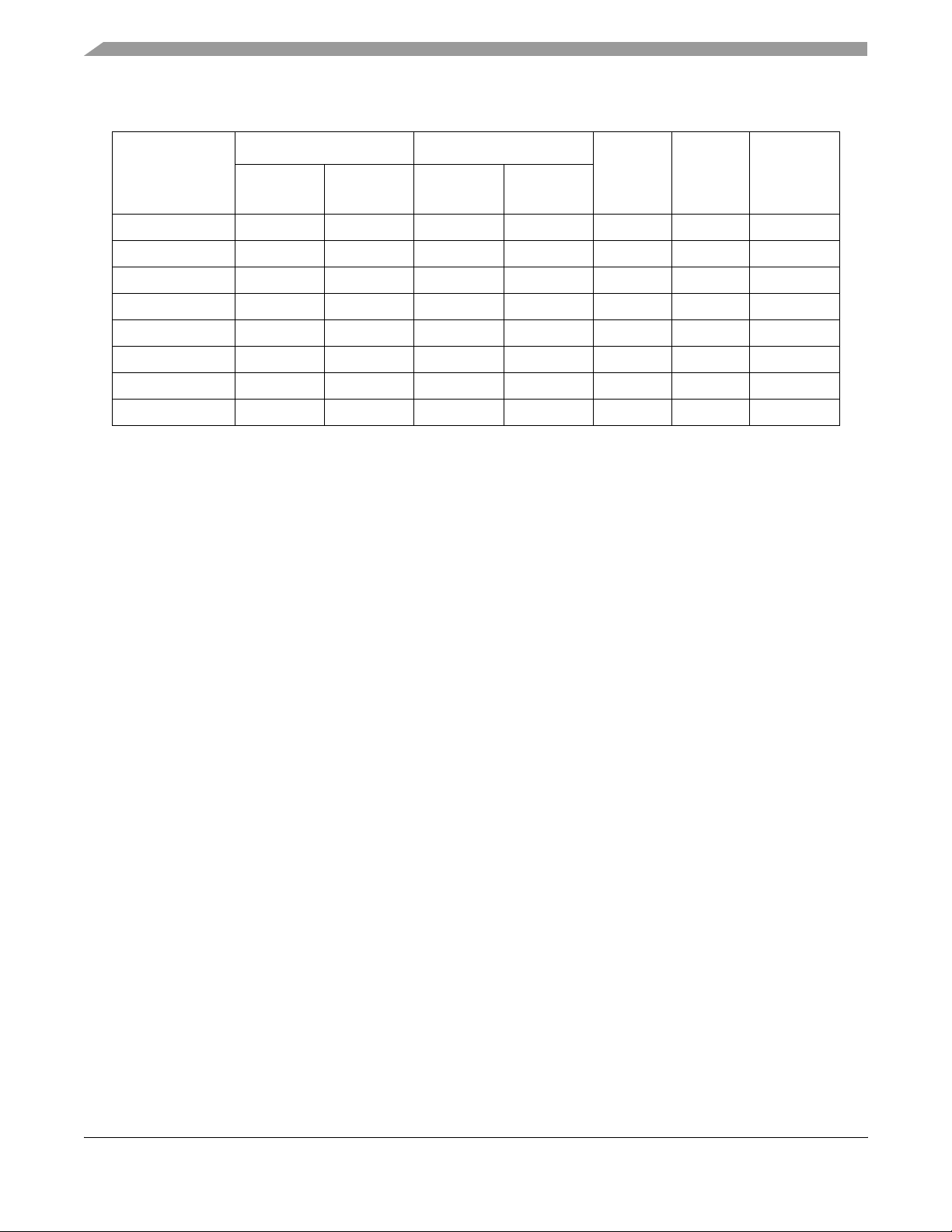
Table 1. MPC860 Family Functionality
Cache (Kbytes) Ethernet
Part
MPC860DE 4 4 Up to 2 — — 2 1
MPC860DT 4 4 Up to 2 1 Yes 2 1
MPC860DP 16 8 Up to 2 1 Yes 2 1
MPC860EN 4 4 Up to 4 — — 4 1
MPC860SR 4 4 Up to 4 — Yes 4 1
MPC860T 4 4 Up to 4 1 Yes 4 1
MPC860P 16 8 Up to 4 1 Yes 4 1
MPC855T 4 4 1 1 Yes 1 2
1
Supporting documentation for these devices refers to the following:
1. MPC860 PowerQUICC Family User’s Manual (MPC860UM, Rev. 3)
2. MPC855T User’s Manual (MPC855TUM/D, Rev. 1)
Instruction
Cache
Data Cache 10T 10/100
ATM SCC Reference
1
2Features
The following list summarizes the key MPC860 features:
• Embedded single-issue, 32-bit PowerPCTM core (implementing the PowerPC architecture) with
thirty-two
— The core performs branch prediction with conditional prefetch without conditional execution.
— 4- or 8-Kbyte data cache and 4- or 16-Kbyte instruction cache (see Table 1)
— MMUs with 32-entry TLB, fully-associative instruction, and data TLBs
— MMUs support multipl e page size s of 4-, 16-, and 512-Kbyt es, and 8-Mbyt es; 16 virtual address spa ces
— Advanced on-chip-emulation debug mode
• Up to 32-bit data bus (dynamic bus sizing for 8, 16, and 32 bits)
• 32 address lines
• Operates at up to 80 MHz
• Memory controller (eight banks)
— Contains complete dynamic RAM (DRAM) controller
32-bit general-purpose registers (GPRs)
– 16-Kbyte instruction cach es are four -way, set-associative with 256 sets ; 4-Kbyt e inst ructi on cache s
are two-way, set-associative with 128 sets.
– 8-Kbyte data caches are two-way, set-associative with 256 sets; 4-Kbyte data caches are two-way,
set-associative with 128 sets.
– Cache coherency for both instruction and data caches is maintained on 128-bit (4-word) cache
blocks.
– Caches are physi cally addresse d, implement a leas t recently u sed (LRU) repl acement algori thm, and
are lockable on a cache block basis.
and 16 protection groups
MPC860 Family Hardware Specifications, Rev. 7
2 Freescale Semiconduct or
Page 3

Features
— Each bank can be a chip select or RAS to support a DRAM bank.
— Up to 15 wait states programmable per memory bank
— Glueless interface to DRAM, SIMMS, SRAM, EPROM, Flash EPROM, and other memory devices
— DRAM controller programmable to support most size and speed memory interfaces
—Four CAS lines, four WE lines, and one OE line
— Boot chip-select available at reset (options for 8-, 16-, or 32-bit memory)
— Variable block sizes (32 Kbyte to 256 Mbyte)
— Selectable write protection
— On-chip bus arbitration logic
• General-purpose timers
— Four 16-bit timers or two 32-bit timers
— Gate mode can enable/disable counting
— Interrupt can be masked on reference match and event capture.
• System integration unit (SIU)
— Bus monitor
— Software watchdog
— Periodic interrupt timer (PIT)
— Low-power stop mode
— Clock synthesizer
— Decrementer, time base, and real-time clock (RTC) from the PowerPC architecture
— Reset controller
— IEEE 1149.1 test access port (JTAG)
• Interrupts
— Seven external interrupt request (IRQ) lines
— 12 port pins with interrupt capability
— 23 internal interrupt sources
— Programmable priority between SCCs
— Programmable highest priority request
• 10/100 Mbps Ethernet support, fully compliant with the IEEE 802.3u Standard (not available when using
ATM over UTOPIA interface)
• ATM support compliant with ATM forum UNI 4.0 specification
— Cell processing up to 50–70 Mbps at 50-MHz system clock
— Cell multiplexing/demultiplexing
— Support of AAL5 and AAL0 protocols on a per-VC basis. AAL0 support enables OAM and software
implementation of other protocols.
— ATM pace control (APC) scheduler, providing direct support for constant bit rate (CBR) and
unspecified bit rate (UBR) and providing control mechanisms enabling software support of available
bit rate (ABR)
— Physical interface support for UTOPIA (10/100-Mbps is not supported with this interface) and
byte-aligned serial (for example, T1/E1/ADSL)
MPC860 Family Hardware Specifications, Rev. 7
Freescale Semiconduc tor 3
Page 4

Features
— UTOPIA-mode ATM supports level- 1 master with cell-level ha ndshake, multi-PHY (up to four p hysical
layer devices), conne ction to 25-, 5 1-, or 155-Mbps fr amers, and UT OPIA/system cloc k ratios of 1 /2 or
1/3.
— Serial-mode ATM connection sup ports transmiss ion convergenc e (TC) function for T1/E1/ADSL li nes,
cell delineation, cell payload scrambling/descrambling, automatic idle/unassigned cell
insertion/stripping, header error control (HEC) generation, checking, and statistics.
• Communications processor module (CPM)
— RISC communications processor (CP)
— Communication-specifi c commands (for example, GRACEFUL STOP TRANSMIT, ENTER HUNT MODE, and
RESTART TRANSMIT)
— Supports continuous mode transmission and reception on all serial channels
— Up to 8 Kbytes of dual-port RAM
— 16 serial DMA (SDMA) channels
— Three parallel I/O registers with open-drain capability
• Four baud-rate generators (BRGs)
— Independent (can be tied to any SCC or SMC)
— Allows changes during operation
— Autobaud support option
• Four serial communi cations controllers (SCCs)
— Ethernet/IEEE 802.3 optional on SCC1–4, supporting full 10-Mbps operation (available only on
specially programmed devices)
— HDLC/SDLC (all channels supported at 2 Mbps)
— HDLC bus (implements an HDLC-based local area network (LAN))
— Asynchronous HDLC to support point-to-point protocol (PPP)
—AppleTalk
— Universal asynchronous receiver transmitter (UART)
— Synchronous UART
— Serial infrared (IrDA)
— Binary synchronous communication (BISYNC)
— Totally transparent (bit streams)
— Totally transparent (frame-based with optional cyclic redundancy check (CRC))
• Two SMCs (serial management channels)
— UART
— Transparent
— General circuit interface (GCI) controller
— Can be connected to the time-division multiplexed (TDM) channels
• One SPI (se rial periphe ral interface)
— Supports master and slave modes
— Supports multimaster operation on the same bus
•One I2C (inter-integrated circuit) port
— Supports master and slave modes
MPC860 Family Hardware Specifications, Rev. 7
4 Freescale Semiconduct or
Page 5

Maximum Tolerated Ratings
— Multiple-master environment support
• Time-slot assigner (TSA)
— Allows SCCs and SMCs to run in multiplexed and/or non-multiplexed operation
— Supports T1, CEPT, PCM highway, ISDN basic rate, ISDN primary rate, user defined
— 1- or 8-bit resolution
— Allows independent transmit and receive routing, frame synchronization, and clocking
— Allows dynamic changes
— Can be internally connected to six serial channels (four SCCs and two SMCs)
• Parallel i nterface port (PIP)
— Centronics interfa ce supp ort
— Supports fast connection between compatible ports on the MPC860 or the MC68360
• PCMCIA interface
— Master (so cket) interface, release 2.1 compliant
— Supports two independent PCMCIA sockets
— Supports eight memory or I/O windows
• Low power support
— Full on—all units fully powered
— Doze—core functional un its disabled except ti me base decrementer , PLL, memory controll er, R TC, and
CPM in low-power standby
— Sleep—all units disabled except RTC and PIT, PLL active for fast wake up
— Deep sleep—all units disabled including PLL except RTC and PIT
— Power down mode—all units powered down except PLL, RTC, PIT, time base, and decrementer
• Debug interface
— Eight comparators: four operate on instruc tion address, two oper ate on data address, and two operate on
data
— Supports conditions: = ≠ < >
— Each watchpoint can generate a break -po int inte rnally.
• 3.3-V operation with 5-V TTL compatibility except EXTAL and EXTCLK
• 357-pin ball grid array (BGA) package
3 Maximum Tolerated Ratings
This section provides the maximum tolerated voltag e and temperature ranges for the MPC860. Table 2 provides the
maximum ratings.
This device contains circuitry protecting against damage due to high-static voltage or electrical fields; however, it
is advised that normal prec autions be taken to avoid applicat ion of any voltages higher than maxi mum-rated voltages
to this high-i mpeda nce ci rcuit. Reliabilit y of operation is enhanced if unused inputs are tied t o a n appropriate logic
voltage level (for example, either GND or V
MPC860 Family Hardware Specifications, Rev. 7
Freescale Semiconduc tor 5
dd
).
Page 6
Thermal Characterist ics
(GND = 0 V)
Supply voltage
Input voltage
1
2
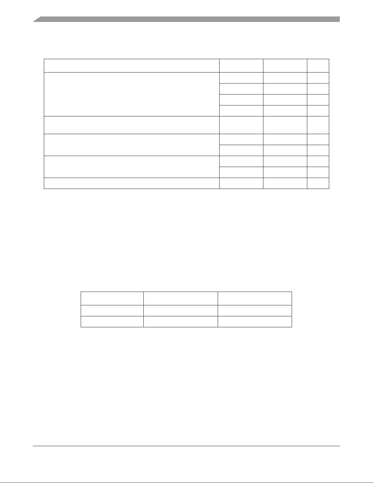
Table 2. Maximum Tolerated Ratings
Rating Symbol Value Unit
V
DDH
V
DDL
KAPWR –0.3 to 4.0 V
VDDSYN –0.3 to 4.0 V
V
in
–0.3 to 4.0 V
–0.3 to 4.0 V
GND – 0.3 to
VDDH
V
Temperature 3 (standard)
Temperature 3 (extended) T
Storage temperature range T
1
The power supply of the device must start its ramp from 0.0 V.
2
Functional operating conditions are provided with the DC electrical specifications in Table 6. Absolute maximum
T
A(min)
T
j(max)
A(min)
T
j(max)
stg
0 °C
95 °C
–40 °C
95 °C
–55 to 150 °C
ratings are stress rat ings only ; functiona l operation at the maxim a is not gua ranteed. Stress beyond those listed may
affect device reliability or cause permanent damage to the device.
Caution: All inputs that tole rate 5 V cannot be more than 2.5 V gre ater than the supply volt age. This restrictio n applies
to power-up and normal operation (that is, if the MPC860 is unpowered, voltage greater than 2.5 V must not be
applied to its inputs).
3
Minimum temperatures are guaranteed as ambient temperature, TA. Maximum temperatures are guaranteed as
junction temperature, T
.
j
4 Thermal Characteristics
Table 3. Package Description
Package Designator Package Code (Case No.) Package Description
ZP 5050 (1103-01) PBGA 357 25*25*0.9P1.27
ZQ / VR 5058 (1103D-02) PBGA 357 25*25*1.2P1.27
Table 4 shows the thermal characteristics for the MPC860.
MPC860 Family Hardware Specifications, Rev. 7
6 Freescale Semiconduct or
Page 7
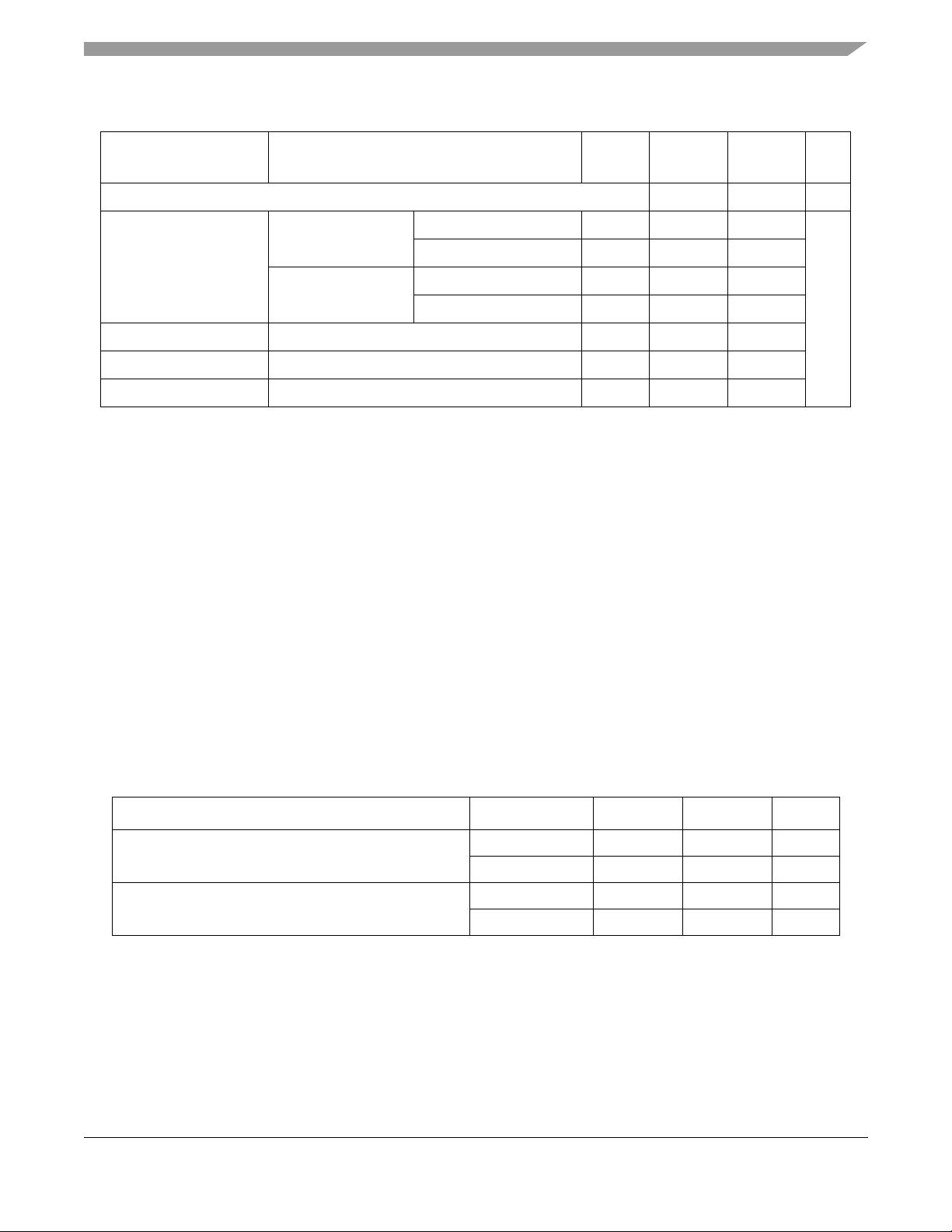
Table 4. MPC860 Thermal Resistance Data
Power Dissipation
Rating Environment Symbol
ZP
MPC860P
ZQ / VR
MPC860P
Unit
Mold Compound Thickness 0.85 1.15 mm
Junction-to-ambient
1
Natural convection Single-layer board (1s) R
Four-layer board (2s2p) R
Airflow (200 ft/min) Single-layer board (1s) R
Four-layer board (2s2p) R
Junction-to-board
Junction-to-case
Junction-to-package top
1
Junction temperature is a function of on-chip power dissipation, package thermal resistance, mounting site (board)
4
5
6
Natural convection Ψ
θJA
θJMA
θJMA
θJMA
R
θJB
R
θJC
2
3
3
3
34 34 °C/W
22 22
27 27
18 18
14 13
6 8
JT
2 2
temperature, ambient temperature, air flow, power dissipation of other components on the board, and board thermal
resistance.
2
Per SEMI G38-87 and JEDEC JESD51-2 with the single layer board horizontal.
3
Per JEDEC JESD51-6 with the board horizontal.
4
Thermal resistan ce between the die and the prin ted circuit board per JEDEC JESD51- 8. Board temperature is measured
on the top surface of the board near the package.
5
Indicates the average thermal resistance between the die and the case top surface as measured by the cold plate
method (MIL SPEC-883 Metho d 1012.1) with the cold plate tempe rature used for the case temperature. F or exposed pad
packages whe re the pad wo uld be expecte d to be soldered , junction-to-ca se thermal resis tance is a simulated val ue from
the junction to the exposed pad without contact resistance.
6
Thermal characterization parameter indicating the temperature difference between the package top and the junction
temperature per JEDEC JESD51-2.
5 Power Dissipation
Table 5 provides power dissipation in for m at ion . The mode s a re 1: 1, where CPU and bus speeds are equal, and 2:1,
where CPU frequency is twice the bus speed.
Table 5. P ow er Dissi pation (PD)
Die Revision Frequency (MHz) Typical
D.4
(1:1 mode)
D.4
(2:1 mode)
1
Typical power dissipation is measured at 3.3 V.
2
Maximum power dissipation is measured at 3.5 V.
Values in Table 5 represent V
power dissipation over V
DDH
due to buffer current, depending on external circuitry.
MPC860 Family Hardware Specifications, Rev. 7
1
Maximum
50 656 735 mW
66 TBD TBD mW
66 722 762 mW
80 851 909 mW
NOTE
-based power dissipatio n and do not include I/O
DDL
. I/O power dissipation varies widely by application
2
Unit
Freescale Semiconduc tor 7
Page 8
DC Characteristics
6 DC Characteristics
Table 6 provides the DC electrical characteristics for the MPC860.
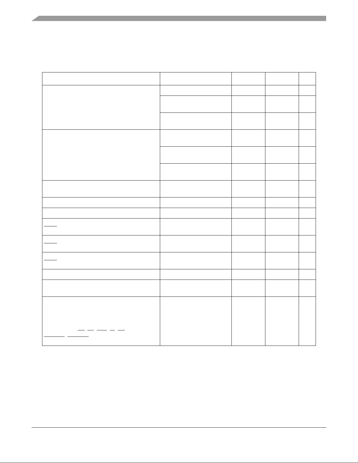
Table 6. DC Electrical Specifications
Characteristic Symbol Min Max Unit
Operating voltage at 40 MHz or less V
DDH
, V
DDL
KAPWR
(power-down mode)
KAPWR
(all other operating mo des)
Operating voltage greater than 40 MHz V
DDH
, V
VDDSYN
KAPWR
(power-down mode)
KAPWR
(all other operating mo des)
Input high voltage (all inputs except EXTAL and
EXTCLK)
Input low voltage
1
EXTAL, EXTCLK input high voltage V
Input leakage current, Vin = 5.5 V (except TMS,
TRST, DSCK, and DSDI pins)
Input leakage current, Vin = 3.6 V (except TMS,
TRST, DSCK, and DSDI pins)
Input leakage current, Vin = 0 V (except TMS,
TRST, DSCK, and DSDI pins)
Input capacitance
Output high voltag e, IOH = –2.0 mA, V
2
= 3.0 V
DDH
(except XTAL, XFC, and open-drain pins)
, VDDSYN 3.0 3.6 V
2.0 3.6 V
V
– 0.4 V
, KAPWR,
DDL
DDH
3.135 3.465 V
DDH
2.0 3.6 V
V
– 0.4 V
DDH
V
IH
V
IL
IHC
I
in
I
In
I
In
C
in
V
OH
2.0 5.5 V
GND 0.8 V
0.7 × (V
DDH
) V
— 100 µA
— 10 µA
— 10 µA
— 20 pF
2.4 — V
DDH
+ 0.3 V
DDH
V
V
Output low voltage
IOL = 2.0 mA, CLKOUT
IOL = 3.2 mA
IOL = 5.3 mA
3
4
V
OL
— 0.5 V
IOL = 7.0 mA, TXD1/PA14, TXD2/PA12
IOL = 8.9 mA, TS, TA, TEA, BI, BB,
HRESET, SRESET
1
VIL(max) for the I2C interface is 0.8 V rather than the 1.5 V as specified in the I2C standard.
2
Input capacitance is periodically sampled.
MPC860 Family Hardware Specifications, Rev. 7
8 Freescale Semiconduct or
Page 9

Thermal Calculation and Measurement
3
A(0:31), TSIZ0/REG, TSIZ1, D(0:31), DP(0:3)/IRQ(3:6), RD/WR, BURST, RSV/IRQ2, IP_B(0:1)/IWP(0:1)/
VFLS(0:1), IP_B2/IOIS16_B/AT2, IP_B3/IWP2/VF2, IP_B4/LWP0/VF0, IP_B5/LWP1/VF1, IP_B6/DSDI/AT0,
IP_B7/PTR/AT3, RXD1 /PA15, RXD2/PA13, L1TXDB/PA11, L1RXDB/PA10, L1TXDA/PA9, L1RXDA/PA8,
TIN1/L1RCLKA/BRGO1/CLK1/PA7, BRGCLK1/
TOUT2/CLK4/PA4, TIN3/BRGO3/CLK5/PA3, BRGCLK2/L1RCLKB/TOUT3/CLK6/PA2, TIN4/BRGO4/CLK7/
P A1, L1TCLKB/TOUT4/CLK8/PA0, REJCT1/SPISEL/PB31, SPICLK/PB30, SPIMOSI/PB29, BRGO4/SPIMISO/
PB28, BRGO1/I2CSDA/PB27, BRGO2/I2CSCL/PB26, SMTXD1/PB25, SMRXD1/PB24, SMSYN1/SDACK1/
PB23, SMSYN2/SDACK2/PB22, SMTXD2/L1CLKOB/PB21, SMRXD2/L1CLKOA/PB20, L1ST1/RTS1/PB19,
L1ST2/
RTS2/PB18, L1ST3/L1RQB/PB17, L1ST4/L1RQA/PB1 6, BRGO3/PB15, RSTRT1/PB14, L1ST1/RTS1/
DREQ0/PC15, L1ST2/RTS2/DREQ1/PC14, L1ST 3/L1RQB/PC13, L1ST4/L1RQA/PC12, CTS1/PC11,
TGATE1/CD1/PC10, CTS2/PC9, TGA TE2/CD2/PC8, SDACK2/L1TSYNCB/PC7, L1RSYNCB/PC6, SDACK1/
L1T SYNCA/PC5, L1RSYNCA/PC4, PD15, PD14, PD13, PD12, PD 1 1, PD10, PD9, PD8, PD5, PD6, PD7, PD4, PD3,
MII_MDC, MII_TX_ER, MII_EN, MII_MDIO, MII_TXD[0:3]
4
BDIP/GPL_B(5), BR, BG, FRZ/IRQ6, CS(0:5), CS(6)/CE(1)_B, CS(7)/CE(2)_B, WE0/BS_B0/IORD,
WE1/BS_B1/IOWR, WE2/BS_B2/PCOE, WE3/BS_B3/PCWE, BS_A(0:3), GPL_A0/GPL_B0, OE/GPL_A1/
GPL_B1, GPL_A(2:3)/GPL_B(2:3)/CS(2:3), UPWAITA/GPL_A4, UPWAITB/GPL_B4, GPL_A5, ALE_A, CE1_A,
CE2_A, ALE_B/DSCK/AT1, OP(0:1), OP2/MODCK1/STS, OP3/MODCK2/DSDO, BADDR(28:30)
TOUT1/CLK2/PA6, TIN2/L1TCLKA/BRGO2/CLK3/PA5,
7 Thermal Calculation and Measurement
For the foll owing discu ssions, PD = (VDD × IDD) + PI/O, where PI/O is the power dissipation of the I/O drivers.
7.1 Estimation with Junction-to-Ambient Thermal Resistance
An estimation of the chip junction temperature, TJ, in °C can be obtained from the equation:
TJ = TA + (R
θJA
× PD)
where:
TA = ambient temperature (ºC)
R
= package j unction-to-a mbient ther mal resistance (ºC/W)
θJA
PD = power dissipation in package
The junction-to-a mbient thermal resis tance is an industry s tandard value whic h provides a quick and eas y estimation
of thermal perform ance. However , the answer is o nly an estimate; t est cases have demo nstrated that err ors of a factor
of two (in the quantity T
– TA) are possible.
J
7.2 Estimation with Junction-to-Case Thermal Resistance
Historically , the thermal resistance has frequently been expressed as the sum of a junction-to-case thermal resistance
and a case-to-ambient thermal resistance:
R
= R
θJA
where:
R
= junction-to-ambient thermal resistance (ºC/W)
θJA
R
= junction-to-case thermal resistance (ºC/W)
θJC
R
= case-to-ambient thermal resistance (ºC/W)
θCA
R
is device related and cannot be influenced by the user. The user adjusts the thermal environment to affect the
θJC
case-to-am bient therm al resistance, R
heat sink, change the mounting arrangement on the printed circuit board, or change the thermal dissipation on the
θJC
+ R
θCA
. For instance, the user can change the air flow around the device, add a
θCA
MPC860 Family Hardware Specifications, Rev. 7
Freescale Semiconduc tor 9
Page 10
Thermal Calculation and Measuremen t
printed circuit boar d surrounding the device. Thi s thermal model is most usefu l for ceramic packages wit h heat sinks
where some 90% of the heat flows through the case and the heat sink to the ambient environment. For most
packages, a better model is required.
7.3 Estimation with Junction-to-Board Thermal Resistance
A simple package thermal mode l which has demonst rated re asonable ac curacy (abo ut 20%) is a two-resi stor model
consisting of a junc ti on-to- board and a ju nctio n-to- case t herma l res ista nce. The j unc tion- to-ca se the rmal re sist ance
covers the situ ation where a heat sink i s u sed or where a subst antia l am ount of heat is di ssipa ted from t he top of the
package. The junction-to-board thermal resistance describes the thermal performance when most of the heat is
conducted to the pri nt ed c ir cui t boa rd. It has been observ ed t hat the thermal perf or mance of most plastic pa cka ges ,
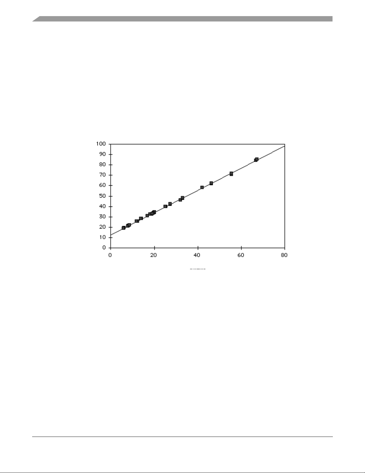
especially PBGA packages, is strongly dependent on the board temperature; see
Figure 1.
Junction Temperature Rise Above
Ambient Divided by Package Power
Board T emperature Rise Above Ambient Divided by Package Power
Figure 1. Effect of Board Temperature Rise on Thermal Behavior
If the board temperature is known, an estimate of the junction temperature in the environment can be made using
the following equation:
TJ = TB + (R
θJB
× PD)
where:
R
= junction-to-board thermal resistance (ºC/W)
θJB
TB = board temperature (ºC)
PD = power dissipation in package
If the board temperature is known and the heat loss from the package case to the air can be ignored, acceptable
predictions of junction temperature can be made. For this method to work, the board and board mounting must be
similar to the test board used to determine the junction-to-board thermal resistance, namely a 2s2p (board with a
power and a ground plane) and by attaching the thermal balls to the ground plane.
MPC860 Family Hardware Specifications, Rev. 7
10 Freescale Semiconduct or
Page 11

Layout Practices
7.4 Estimation Using Simulation
When the board temperatur e is not known, a therma l simulation of the appl ication is needed . The simple two-resistor
model can be used with the therma l simula tion of t he app licat ion [2] , or a more ac curate and co mple x model of the
package can be used in the thermal simulation.
7.5 Experimental Determination
To determine the junction temperature of the device in the application after prototypes are available, the thermal
characterization parameter (Ψ
temperature at the top center of the package case using the following equation:
TJ = TT + (ΨJT × PD)
where:
Ψ
= thermal characterization parameter
JT
TT = thermocouple temperature on top of package
PD = power dissipation in package
The thermal characterization parameter is measured per JEDEC JESD51-2 specification using a 40 gauge type T
thermocouple epoxied to the top center of the package case. The thermocouple should be positioned so that the
thermocouple juncti on rests on the p ackage. A small a mount of ep oxy is placed o ver the thermocoupl e juncti on and
over 1 mm of wire extending from the junction. The thermocouple wire is placed flat against the package case to
avoid measurement errors caused by cooling effects of the thermocouple wire.
) can be use d to determine the junction temperature with a measurement of the
JT
7.6 References
Semiconductor Equipment and Materials International (415) 964-5111
805 East Middlefield Rd.
Mountain View, CA 94043
MIL-SPEC and EIA/JESD (JEDEC) Specifications 800-854-7179 or
(Available from Global Engineering Documents) 303-397-7956
JEDEC Specifications http://www.jedec.org
1. C.E. Triplett and B. Joiner, “An Experimental Characterization of a 272 PBGA Within an Automotive
Engine Controller Module,” Proceedings of SemiTherm, San Diego, 1998, pp. 47–54.
2. B. Joiner and V. Adams, “Measurement and Simulation of Junction to Board Thermal Resistance and Its
Application in Thermal Modeling,” Proceedings of SemiTherm, San Diego, 1999, pp. 212–220.
8 Layout Practices
Each VDD pin on the MPC860 should be provided with a low-impe dance path to th e board’s supply. Each GND pin
should likewise be provided with a low-impedance path to ground. The power supply pins drive distinct groups of
logic on the chip. The V
located as close as possible to the four sides of t he package. The capa citor leads and associated printed circ uit traces
connecting to chip V
employing two inner layers as V
power supply should be bypasse d to groun d using at least four 0.1 µF-bypass capacitors
DD
and GND should be kept to less than half an inch per capacitor lead. A four-layer board
DD
and GND planes is recommended.
CC
MPC860 Family Hardware Specifications, Rev. 7
Freescale Semiconduc tor 11
Page 12
Bus Signal Timing
All output pins on the MPC860 have fa st rise and fall times. Printed c ircuit (PC) tr ace interc onnection le ngth should
be minimized in order to minimize undershoot and reflections caused by these fast output switching times. This
recommendation particularly applies to the address and data buses. Maximum PC trace lengths of 6 inches are
recommended. Capaci tance calc ulations s hould conside r all devi ce loads as well as pa rasitic c apacitances due to the
PC traces. Attention to proper PCB layout and bypassing becomes especially critical in systems with higher
capacitive loads because these loads create higher transient currents in the V
and GND circuits. Pull up all unused
CC
inputs or signals that will be inputs during reset. Special care should be taken to minimize the noise levels on the
PLL supply pins.
9 Bus Signal Timing
Table 7 provides the bus operation timing for the MPC860 at 33, 40, 50, and 66 MHz.
The maximum bus speed supported by the MPC860 i s 6 6 MHz. Hi ghe r-speed parts must be operated in half -s pee d
bus mode (for example, an MPC860 used at 80 MHz must be configured for a 40 MHz bus).
The timing for the MPC860 bus shown assumes a 50-pF load for maximum delays and a 0-pF load for minimum
delays.
Table 7. Bus Operation Timings
33 MHz 40 MHz 50 MHz 66 MHz
Num Characteristic
Min Max Min Max Min Max Min Max
Unit
B1 CLKOUT period 30.30 30.30 25.00 30.30 20.00 30.30 15.15 30.30 ns
B1a EXTCLK to CLKOUT phase skew
(EXTCLK > 15 MHz and MF <= 2)
B1b EXTCLK to CLKOUT phase skew
(EXTCLK > 10 MHz and MF < 10)
B1c CLKOUT phase jitter (EXTCLK >
15 MHz and MF <= 2)
B1d CLKOUT phase jitter
B1e CLKOUT frequency jitte r (M F < 1 0) 1— 0.50 — 0.50 — 0.50 — 0.50 %
B1f CLKOUT frequency jitter (10 < MF
B1g CLKOUT frequency jitter ( MF > 500) 1— 3.00 — 3.00 — 3.00 — 3.00 %
B1h Frequency jitter on EXTCLK
B2 CLKOUT pulse width low 12.12 — 10.00 — 8.00 — 6.06 — ns
B3 CLKOUT width high 12.12 — 10.00 — 8.00 — 6.06 — ns
B4 CLKOUT rise time
B533CLKOUT fall time
B7 CLKOUT to A(0:31), BADDR(28:30),
1
500)
<
WR, BURST, D(0:3 1), DP(0:3)
RD/
invalid
1
1
2
3
3
–0.90 0.90 –0.90 0.90 –0.90 0.90 –0.90 0.90 ns
–2.30 2.30 –2.30 2.30 –2.30 2.30 –2.30 2.30 ns
–0.60 0.60 –0.60 0.60 –0.60 0.60 –0.60 0.60 ns
–2.00 2.00 –2.00 2.00 –2.00 2.00 –2.00 2.00 ns
— 2.00 — 2.00 — 2.00 — 2.00 %
— 0.50 — 0.50 — 0.50 — 0.50 %
— 4.00 — 4.00 — 4.00 — 4.00 ns
— 4.00 — 4.00 — 4.00 — 4.00 ns
7.58 — 6.25 — 5.00 — 3.80 — ns
MPC860 Family Hardware Specifications, Rev. 7
12 Freescale Semiconduct or
Page 13
Num Characteristic
Bus Signal Timing
Table 7. Bus Operation Timings (continued)
33 MHz 40 MHz 50 MHz 66 MHz
Unit
Min Max Min Max Min Max Min Max
B7a CLKOUT to TSIZ(0:1), REG, RSV,
AT(0:3),
BDIP, PTR invalid
B7b CLKOUT to BR, BG, FRZ,
VFLS(0:1), VF(0:2) IWP(0:2),
LWP(0:1), STS invalid
4
B8 CLKOUT to A(0:31), BADDR(28:30)
WR, BURST, D(0:3 1), DP(0:3)
RD/
7.58 — 6.25 — 5.00 — 3.80 — ns
7.58 — 6.25 — 5.00 — 3.80 — ns
7.58 14.33 6.25 13.00 5.00 11.75 3.80 10.04 ns
valid
B8a CLKOUT to TSIZ(0:1), REG, RSV,
AT(0:3)
BDIP, PTR valid
B8b CLKOUT to BR, BG, VFLS(0:1),
VF(0:2), IWP(0:2), FRZ, LWP(0:1),
STS valid
4
B9 CLKOUT to A(0:31), BADDR(28:30),
WR, BURST, D(0:3 1), DP(0:3),
RD/
TSIZ(0:1),
REG, RSV, AT(0:3), PTR
7.58 14.33 6.25 13.00 5.00 11.75 3.80 10.04 ns
7.58 14.33 6.25 13.00 5.00 11.75 3.80 10.04 ns
7.58 14.33 6.25 13.00 5.00 11.75 3.80 10.04 ns
High-Z
B11 CLKOUT to TS, BB assertion 7.58 13.58 6.25 12.25 5.00 11.00 3.80 11.29 ns
B11a CLKOUT to TA, BI assertion (when
2.50 9.25 2.50 9.25 2.50 9.25 2.50 9.75 ns
driven by the memory control ler or
PCMCIA interface)
B12 CLKOUT to TS, BB negation 7.58 14.33 6.25 13.00 5.00 11.75 3.80 8.54 ns
B12a CLKOUT to TA, BI negation (when
2.50 11.00 2.50 11.00 2.50 11.00 2.50 9.00 ns
driven by the memory control ler or
PCMCIA interface)
B13 CLKOUT to TS, BB High-Z 7.58 21.58 6.25 20.25 5.00 19.00 3.80 14.04 ns
B13a CLKOUT to TA, BI High-Z (when
2.50 15.00 2.50 15.00 2.50 15.00 2.50 15.00 ns
driven by the memory control ler or
PCMCIA interface)
B14 CLKOUT to TEA assertion 2.50 10.00 2.50 10.00 2.50 10.00 2.50 9.00 ns
B15 CLKOUT to TEA High-Z 2.50 15.00 2.50 15.00 2.50 15.00 2.50 15.00 ns
B16 TA, BI valid to CLKOUT (setup time) 9.75 — 9.75 — 9.75 — 6.00 — ns
B16a TEA, KR, RETRY, CR valid to
10.00 — 10.00 — 10.00 — 4.50 — ns
CLKOUT (setup time)
B16b BB, BG, BR, valid to CLKOUT (setup
time)
5
B17 CLKOUT to TA, TEA, BI, BB, BG, BR
8.50 — 8.50 — 8.50 — 4.00 — ns
1.00 — 1.00 — 1.00 — 2.00 — ns
valid (hold time)
B17a CLKOUT to KR, RETRY, CR valid
2.00 — 2.00 — 2.00 — 2.00 — ns
(hold time)
MPC860 Family Hardware Specifications, Rev. 7
Freescale Semiconduc tor 13
Page 14
Bus Signal Timing
Num Characteristic
Table 7. Bus Operation Timings (continued)
33 MHz 40 MHz 50 MHz 66 MHz
Unit
Min Max Min Max Min Max Min Max
B18 D(0:31), DP(0:3) valid to CLKOUT
rising edge (setup tim e)
B19 CLKOUT rising edge to D(0:31),
DP(0:3) valid (hold time)
B20 D(0:31), DP(0:3) valid to CLKOUT
falling edge (setup time)
B21 CLKOUT falling edge to D(0:31),
DP(0:3) valid (hold time)
6
6
7
7
B22 CLKOUT rising edge t o CS asserted
GPCM ACS = 00
B22a CLKOUT fall ing edge to CS assert ed
GPCM ACS = 10, TRLX = 0
B22b CLKOUT fall ing edge to CS assert ed
GPCM ACS = 11, TRLX = 0,
EBDF = 0
B22c CLKOUT falling edge to CS asserted
GPCM ACS = 11, TRLX = 0,
= 1
EBDF
B23 CLKOUT rising edge to CS negated
GPCM read access, GPCM write
access ACS = 00, TRLX = 0, and
CSNT = 0
6.00 — 6.00 — 6.00 — 6.00 — ns
1.00 — 1.00 — 1.00 — 2.00 — ns
4.00 — 4.00 — 4.00 — 4.00 — ns
2.00 — 2.00 — 2.00 — 2.00 — ns
7.58 14.33 6.25 13.00 5.00 11.75 3.80 10.04 ns
— 8.00 — 8.00 — 8.00 — 8.00 ns
7.58 14.33 6.25 13.00 5.00 11.75 3.80 10.54 ns
10.86 17.99 8.88 16.00 7.00 14.13 5.18 12.31 ns
2.00 8.00 2.00 8.00 2.00 8.00 2.00 8.00 ns
B24 A(0:31) and BADDR(28:30) to CS
5.58 — 4.25 — 3.00 — 1.79 — ns
asserted GPCM ACS = 10,
TRLX = 0
B24a A(0:31) and BADDR(28:30) to CS
asserted GPCM ACS = 11, TRLX =
B25 CLKOUT rising edge to OE, WE(0:3)
13.15 — 10.50 — 8.00 — 5.58 — ns
0
— 9.00 — 9.00 — 9.00 — 9.00 ns
asserted
B26 CLKOUT rising edge to OE negated 2.00 9.00 2.00 9.00 2.00 9.00 2.00 9.00 ns
B27 A(0:31) and BADDR(28:30) to CS
asserted GPCM ACS = 10, TRLX =
B27a A(0:31) and BADDR(28:30) to CS
asserted GPCM ACS = 11, TRLX =
B28 CLKOUT rising edge to WE(0:3)
35.88 — 29.25 — 23.00 — 16.94 — ns
1
43.45 — 35.50 — 28.00 — 20.73 — ns
1
— 9.00 — 9.00 — 9.00 — 9.00 ns
negated GPCM write access
CSNT = 0
B28a CLKOUT falling edge to WE(0:3)
7.58 14.33 6.25 13.00 5.00 11.75 3.80 10.54 ns
negated GPCM write access
TRLX = 0, 1, CSNT = 1, EBDF = 0
MPC860 Family Hardware Specifications, Rev. 7
14 Freescale Semiconduct or
Page 15

Num Characteristic
Bus Signal Timing
Table 7. Bus Operation Timings (continued)
33 MHz 40 MHz 50 MHz 66 MHz
Unit
Min Max Min Max Min Max Min Max
B28b CLKOUT fal ling edge to CS neg ated
GPCM write access TRLX = 0, 1,
CSNT = 1, ACS = 10, or ACS = 11,
EBDF = 0
B28c CLKOUT falling edge to WE(0:3)
negated GPCM write access
TRLX = 0, 1, CSNT = 1 write access
= 0, CSNT = 1, EBDF = 1
TRLX
B28d CLKOUT fal ling edge to CS neg ated
GPCM write access TRLX = 0, 1,
CSNT = 1, ACS = 10, or ACS = 11,
EBDF = 1
B29 WE(0:3) negated to D(0:31), DP(0:3)
High-Z GPCM write access
CSNT = 0, EBDF = 0
B29a WE(0:3) negated to D(0:31), DP(0:3)
High-Z GPCM write access,
= 0, CSNT = 1, EBDF = 0
TRLX
B29b CS negated to D(0:31), DP(0:3),
High-Z GPCM write access,
ACS = 00, TRLX = 0, 1, an d CSNT =
0
B29c CS negated to D(0:31), DP(0:3)
High-Z GPCM write access,
TRLX = 0, CSNT = 1, AC S = 10, or
= 11, EBDF = 0
ACS
— 14.33 — 13.00 — 11.75 — 10.54 ns
10.86 17.99 8.88 16.00 7.00 14.13 5.18 12.31 ns
— 17.99 — 16.00 — 14.13 — 12.31 ns
5.58 — 4.25 — 3.00 — 1.79 — ns
13.15 — 10.5 — 8.00 — 5.58 — ns
5.58 — 4.25 — 3.00 — 1.79 — ns
13.15 — 10.5 — 8.00 — 5.58 — ns
B29d WE(0:3) negated to D(0:31), DP(0:3)
High-Z GPCM write access,
TRLX = 1, CSNT = 1, EBDF = 0
B29e CS negated to D(0:31), DP(0:3)
High-Z GPCM write access,
TRLX = 1, CSNT = 1, AC S = 10, or
ACS = 11, EBDF = 0
B29f WE(0:3) negated to D (0:31), DP(0:3)
High-Z GPCM write access,
TRLX = 0, CSNT = 1, EBDF = 1
B29g CS negated to D(0:31), DP(0:3)
High-Z GPCM write access,
= 0, CSNT = 1, ACS = 10, or
TRLX
ACS = 11, EBDF = 1
B29h WE(0:3) negated to D(0:31), DP(0:3)
High-Z GPCM write access,
= 1, CSNT = 1, EBDF = 1
TRLX
MPC860 Family Hardware Specifications, Rev. 7
Freescale Semiconduc tor 15
43.45 — 35.5 — 28.00 — 20.73 — ns
43.45 — 35.5 — 28.00 — 29.73 — ns
8.86 — 6.88 — 5.00 — 3.18 — ns
8.86 — 6.88 — 5.00 — 3.18 — ns
38.67 — 31.38 — 24.50 — 17.83 — ns
Page 16

Num Characteristic
Table 7. Bus Operation Timings (continued)
33 MHz 40 MHz 50 MHz 66 MHz
Unit
Min Max Min Max Min Max Min Max
B29i CS negated to D(0:31), DP(0:3)
High-Z GPCM write access,
How to Reach Us:
Home Page:
www.freescale.com
email:
support@freescale.com
USA/Europe or Locations Not List e d:
Freescale Semiconductor
Techn ical Information Center, CH370
1300 N. Alma School Road
Chandler, Arizona 85224
(800) 521-6274
480-768-2130
support@freescale.com
Europe, Middle East, and Africa:
Freescale Halbleiter Deutschland GmbH
Techn ical Information Center
Schatzbogen 7
81829 Muenchen, Germany
+44 1296 380 456 (English)
+46 8 52200080 (English)
+49 89 92103 559 (German)
+33 1 69 35 48 48 (French)
support@freescale.com
Japan:
Freescale Semiconductor Japan Ltd.
Techn ical Information Center
3-20-1, Minami-Azabu, Minato-ku
Tokyo 106-0047 Japan
0120 191014
+81 3 3440 3569
support.japan@freescale.com
Asia/Pacific:
Freescale Semiconductor Hong Kong Ltd.
Techn ical Information Center
2 Dai King Street
Tai Po Industrial Estate,
Tai Po, N.T., Hong Kong
+800 2666 8080
support.asia@freescale.com
For Literature Requests Only:
Freescale Semiconductor
Literature Distribution Center
P.O. Box 5405
Denver, Colorado 80217
(800) 441-2447
303-675-2140
Fax: 303-675-2150
LDCForFreescaleSemiconductor@
hibbertgroup.com
TRLX = 1, CSNT = 1, AC S = 10, or
= 11, EBDF = 1
ACS
38.67 — 31.38 — 24.50 — 17.83 — ns
Information in this document is provided solely to enable system and software implementers to
use Freescale Semiconductor products. There are no express or implied copyright licenses
granted hereunder to design or fabricate any integrated circuits or integrated circuits based on the
information in this document.
Freescale Semiconductor reserves the right to make changes without further notice to any
products herein. Freescale Semiconductor makes no warranty, representation or guarantee
regarding the suitability of its products for any particular purpose, nor does Freescale
Semiconductor assume any liability arising out of the application or use of any product or circuit,
and specifically disclaims any and all liability, including without limitation consequential or
incidental damages. “Typical” parameters which may be provided in Freescale Semiconductor
data sheets and/or specifications can and do vary in different applications and actual performance
may vary over time. All operating parameters, including “Typicals” must be validated for each
customer application by customer’s technical experts. Freescale Semiconductor does not convey
any license under its patent rights nor the rights of others. Freescale Semiconductor products are
not designed, intended, or authorized for use as components in systems intended for surgical
implant into the body, or other applications intended to support or sustain life, or for any other
application in which the failure of the Freescale Semiconductor product could create a situation
where personal injury or death may occur. Should Buyer purchase or use Freescale
Semiconductor products for any such unintended or unauthorized application, Buyer shall
indemnify and hold Freescale Semiconductor and its officers, employees, subsidiaries, affiliates,
and distributors harmless against all claims, costs, damages, and expenses, and reasonable
attorney fees arising out of, directly or indirectly, any claim of personal injury or death associated
with such unintended or unauthorized use, even if such claim alleges that Freescale
Semiconductor was negligent regarding the design or manufacture of the part.
Freescale™ and the Freescale logo are trademarks of Freescale Semiconductor, Inc. The
PowerPC name is a trademark of IBM Corp. and is used under license. All other product or service
names are the property of their respective owners.
© Freescale Semiconductor, Inc. 2004.
MPC860EC
Rev. 7
09/2004
Page 17
Num Characteristic
Bus Signal Timing
Table 7. Bus Operation Timings (continued)
33 MHz 40 MHz 50 MHz 66 MHz
Unit
Min Max Min Max Min Max Min Max
B30 CS, WE(0:3) negated to A(0:31),
BADDR(28:30) invalid GPCM write
8
access
B30a WE(0:3) negated to A(0:31),
BADDR(28:30) invalid GPCM, write
access, TRLX = 0, CSNT = 1,
CS negated to A(0:31) inv alid GPCM
write access, TRLX = 0, CSNT =1
ACS = 10, or ACS = 11, EBDF = 0
B30b WE(0:3) negated to A(0:31),
invalid GPCM BADDR(28:3 0) invalid
GPCM write access, TRLX = 1,
CSNT = 1.
CS negated to A(0:31),
Invalid GPCM, write access,
TRLX = 1, CSNT = 1, AC S = 10, or
ACS = 11, EBDF = 0
B30c WE(0:3) negated to A(0:31),
BADDR(28:30) invalid GPCM write
access, TRLX = 0, CSNT = 1.
CS negated to A(0:31) inv alid GPCM
write access, TRLX = 0, CSNT = 1,
ACS = 10, ACS = 11, EBDF = 1
B30d WE(0:3) negated to A(0:31),
BADDR(28:30) invalid GPCM write
access, TRLX = 1, CSNT =1.
CS negated to A(0:31) inv alid GPCM
write access TRLX = 1, CSNT = 1,
ACS = 10, or ACS = 11, EBDF = 1
5.58 — 4.25 — 3.00 — 1.79 — ns
13.15 — 10.50 — 8.00 — 5.58 — ns
43.45 — 35.50 — 28.00 — 20.73 — ns
8.36 — 6.38 — 4.50 — 2.68 — ns
38.67 — 31.38 — 24.50 — 17.83 — ns
B31 CLKOUT falling edge to CS
1.50 6.00 1.50 6.00 1.50 6.00 1.50 6.00 ns
valid—as requested by control bit
CST4 in the corresponding word in
UPM
B31a CLKOUT falling edge to CS
7.58 14.33 6.25 13.00 5.00 11.75 3.80 10.54 ns
valid—as requested by control bit
CST1 in the corresponding word in
UPM
B31b CLKOUT rising edg e to CS valid—as
1.50 8.00 1.50 8.00 1.50 8.00 1.50 8.00 ns
requested by control b it CS T2 in th e
corresponding word in UPM
B31c CLKOUT rising edge to CS val id—as
7.58 14.33 6.25 13.00 5.00 11.75 3.80 10.04 ns
requested by control b it CS T3 in th e
corresponding word in UPM
MPC860 Family Hardware Specifications, Rev. 7
Freescale Semiconduc tor 17
Page 18
Bus Signal Timing
Num Characteristic
Table 7. Bus Operation Timings (continued)
33 MHz 40 MHz 50 MHz 66 MHz
Unit
Min Max Min Max Min Max Min Max
B31d CLKOUT falling edge to CS
valid—as requested by control bit
CST1 in the corresponding word in
UPM, EBDF = 1
B32 CLKOUT falling edge to BS
valid—as requested by control bit
BST4 in the corresponding word in
UPM
B32a CLKOUT falling edge to BS
valid—as requested by control bit
BST1 in the corresponding word in
UPM, EBDF = 0
B32b CLKOUT risi ng edge to BS valid—as
requested by control bit BST2 in the
corresponding word in UPM
B32c CLKOUT rising edge to BS valid—as
requested by control bit BST3 in the
corresponding word in UPM
B32d CLKOUT falling edge to BS
valid—as requested by control bit
BST1 in the corresponding word in
UPM, EBDF = 1
B33 CLKOUT falling edge to GPL
valid—as requested by control bit
GxT4 in the corresponding word in
UPM
13.26 17.99 11.28 16.00 9.40 14.13 7.58 12.31 ns
1.50 6.00 1.50 6.00 1.50 6.00 1.50 6.00 ns
7.58 14.33 6.25 13.00 5.00 11.75 3.80 10.54 ns
1.50 8.00 1.50 8.00 1.50 8.00 1.50 8.00 ns
7.58 14.33 6.25 13.00 5.00 11.75 3.80 10.54 ns
13.26 17.99 11.28 16.00 9.40 14.13 7.58 12.31 ns
1.50 6.00 1.50 6.00 1.50 6.00 1.50 6.00 ns
B33a CLKOUT rising edge to GPL
valid—as requested by control bit
GxT3 in the corresponding word in
UPM
B34 A(0:31), BADDR(28:3 0), and D(0:31)
to
CS valid—as requested by con trol
bit CST4 in the corresponding word
in UPM
B34a A(0:31), BADDR(28:3 0), and D(0:31)
to
CS valid—as requested by con trol
bit CST1 in the corresponding word
in UPM
B34b A(0:31), BADDR(28:3 0), and D(0:31)
to
CS valid—as requested by con trol
bit CST2 in the corresponding word
in UPM
MPC860 Family Hardware Specifications, Rev. 7
18 Freescale Semiconduct or
7.58 14.33 6.25 13.00 5.00 11.75 3.80 10.54 ns
5.58 — 4.25 — 3.00 — 1.79 — ns
13.15 — 10.50 — 8.00 — 5.58 — ns
20.73 — 16.75 — 13.00 — 9.36 — ns
Page 19
Num Characteristic
Bus Signal Timing
Table 7. Bus Operation Timings (continued)
33 MHz 40 MHz 50 MHz 66 MHz
Unit
Min Max Min Max Min Max Min Max
B35 A(0:31), BADDR(28:30) to CS
valid—as requested by control bit
BST4 in the corresponding word in
UPM
B35a A(0:31), BADDR(28:3 0), and D(0:31)
BS valid—as reques ted by control
to
bit BST1 in the corresponding word
in UPM
B35b A(0:31), BADDR(28:3 0), and D(0:31)
BS valid—as reques ted by control
to
bit BST2 in the corresponding word
in UPM
B36 A(0:31), BADDR(28:30), and D(0: 31)
GPL valid—as requested by
to
control bit GxT4 in the corres ponding
word in UPM
B37 UPWAIT valid to CLKOUT falling
B38 CLKOUT falling edge to UPWAIT
B39 AS valid to CLKOUT rising edge
edge
valid
9
9
10
B40 A(0:31), TSIZ(0:1), RD/WR, BURST,
valid to CLKOUT rising edge
5.58 — 4.25 — 3.00 — 1.79 — ns
13.15 — 10.50 — 8.00 — 5.58 — ns
20.73 — 16.75 — 13.00 — 9.36 — ns
5.58 — 4.25 — 3.00 — 1.79 — ns
6.00 — 6.00 — 6.00 — 6.00 — ns
1.00 — 1.00 — 1.00 — 1.00 — ns
7.00 — 7.00 — 7.00 — 7.00 — ns
7.00 — 7.00 — 7.00 — 7.00 — ns
B41 TS valid to CLKOUT rising edge
7.00 — 7.00 — 7.00 — 7.00 — ns
(setup time)
B42 CLKOUT rising edge to TS valid
2.00 — 2.00 — 2.00 — 2.00 — ns
(hold time)
B43 AS negation to memory controller
— TBD — TBD — TBD — TBD ns
signals negation
1
Phase and frequency jitter performance results are only valid if the input jitter is less than the prescribed value.
2
If the rate of change of the fre quency of EXTAL is slow (that is, it does not jump b etween the minim um and maxi mum
values in one cycle) or the frequency of the jitter is fast (that is, it does not stay at an extreme value for a long time)
then the maximum allowed jitter on EXTAL can be up to 2%.
3
The timings specified in B4 and B5 are based on full strength clock.
4
The timing for BR output is relevant when the MPC860 is selected to work with external bus arbiter. The timing for
BG output is relevant when the MPC860 is selected to work with internal bus arbiter.
5
The timing required fo r BR input is relevant when the MPC860 is selected to work with internal bus arbiter . The timing
for
BG input is relevant when the MPC860 is selected to work with external bus arbiter.
6
The D(0:31) and DP(0:3) input timings B18 and B19 refer to the rising edge of the CLKOUT in which the TA input
signal is asserted.
7
The D(0:31) and DP(0:3) in put timing s B20 and B21 refer to the fa lling edge of t he CLKOUT. This timing is valid only
for read accesses con trolled by chip-sel ects u nder control of the UPM in th e memory c ontroller, for data beats where
DLT3 = 1 in the UPM RAM words. (This is only the case where data is latched on the falling edge of CLKOUT.)
MPC860 Family Hardware Specifications, Rev. 7
Freescale Semiconduc tor 19
Page 20
Bus Signal Timing
8
The timing B30 refers to CS when ACS = 00 and to WE(0:3) when CSNT = 0.
9
The signal UPW AIT i s cons idered async hronou s to the CLKO UT an d sync hronized inte rnally. The timings specified
in B37 and B38 are specified to enable the freeze of the UPM output signals as described in Figure 17.
10
The AS si gnal is consid ered asynch ronous to the C LKOUT. The timing B39 is spec ified in order t o allow the b ehavior
specified in Figure 20.
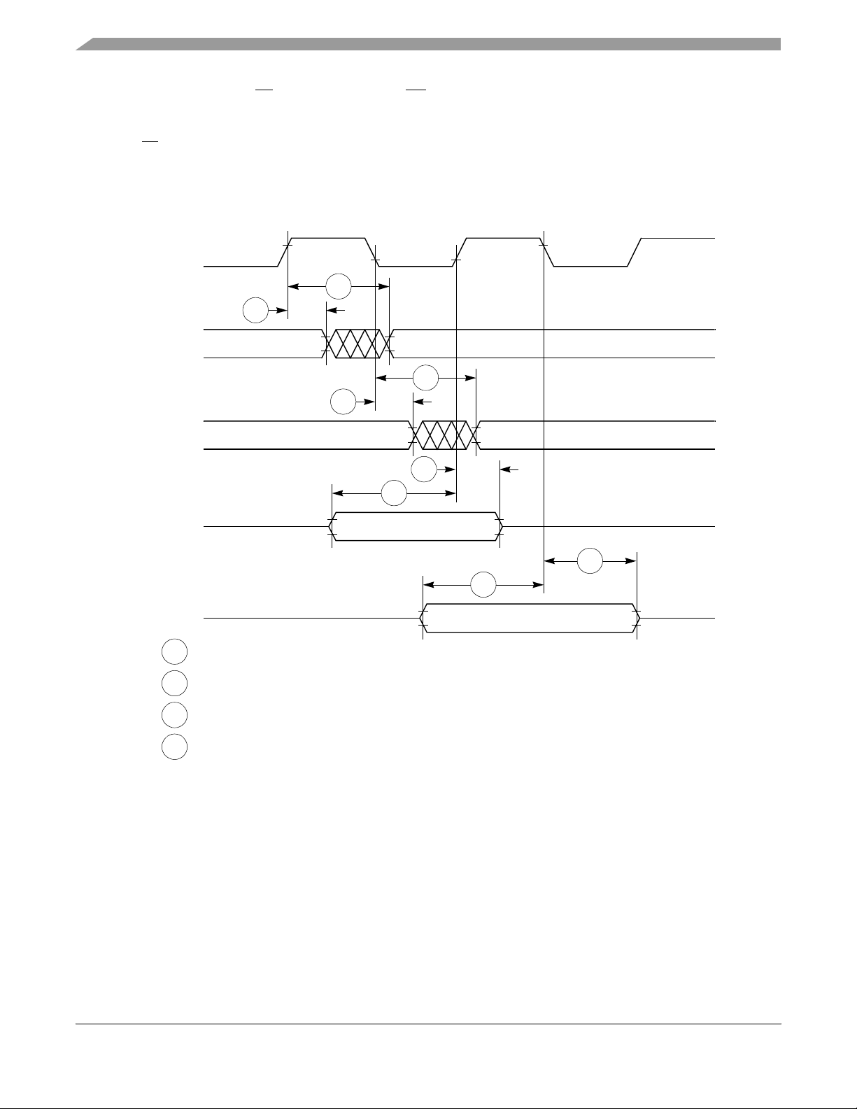
Figure 2 is the control timing diagram.
CLKOUT
Outputs
Outputs
Inputs
Inputs
2.0 V
B
2.0 V
0.8 V
0.8 V
A
B
2.0 V
0.8 V
2.0 V
0.8 V
C
2.0 V
0.8 V
0.8 V
A
D
2.0 V
0.8 V
2.0 V
2.0 V
0.8 V
2.0 V
0.8 V
D
C
2.0 V
0.8 V
A Maximum output delay specification
B Minimum output hold time
C Minimum input se tup tim e spe cif ic atio n
D Minimum input hold time specification
Figure 2. Control Timing
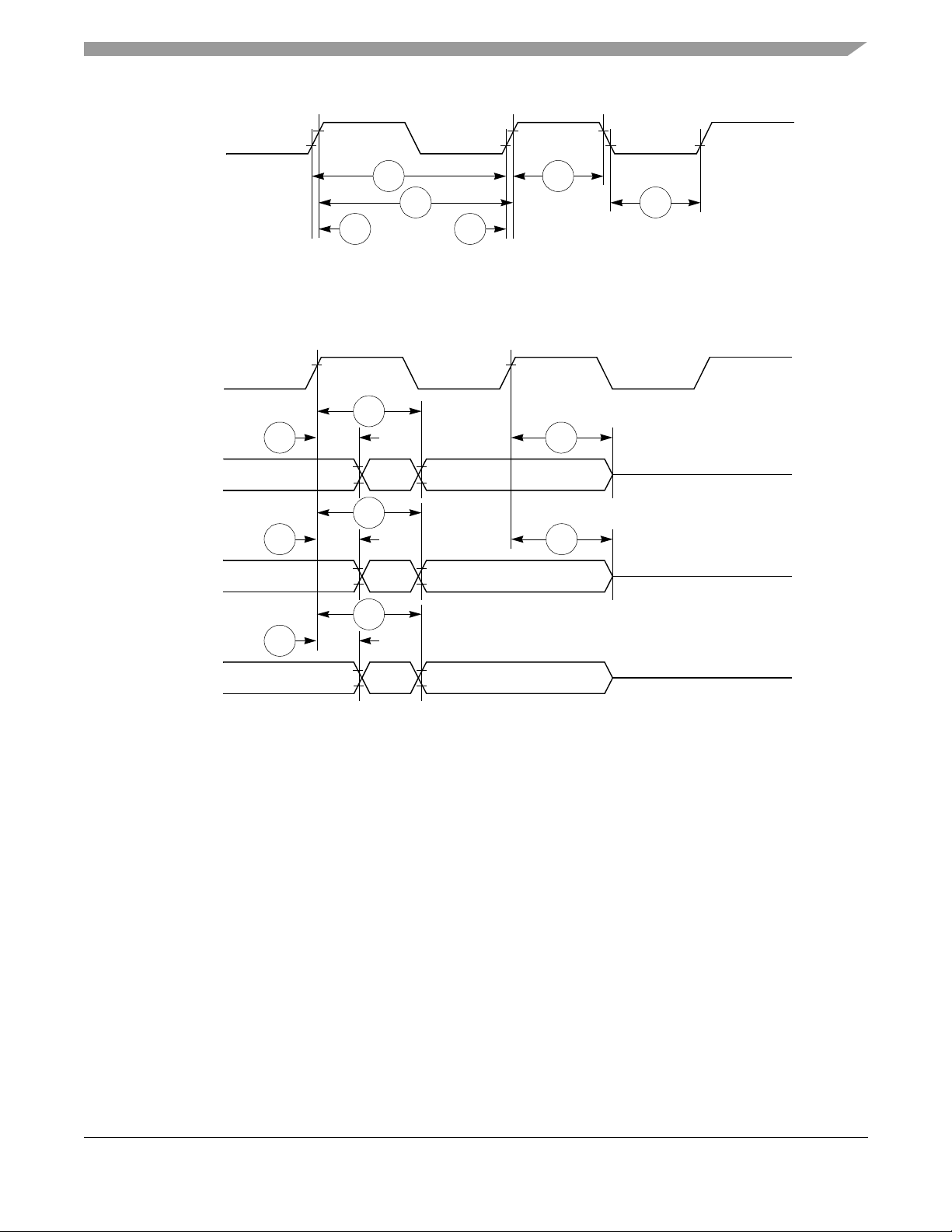
Figure 3 provides the timing for the external clock.
MPC860 Family Hardware Specifications, Rev. 7
20 Freescale Semiconduct or
Page 21
C
LKOUT
C
Bus Signal Timing
B1
B1
B4
B5
Figure 3. External Clock Timing
Figure 4 provides the timing for the synchronous output signals.
LKOUT
B8
B7 B9
Output
Signals
B8a
Output
Signals
B8b
B3
B2
B9B7a
B7b
Output
Signals
Figure 4. Synchronous Output Signals Timing
MPC860 Family Hardware Specifications, Rev. 7
Freescale Semiconduc tor 21
Page 22
Bus Signal Timing
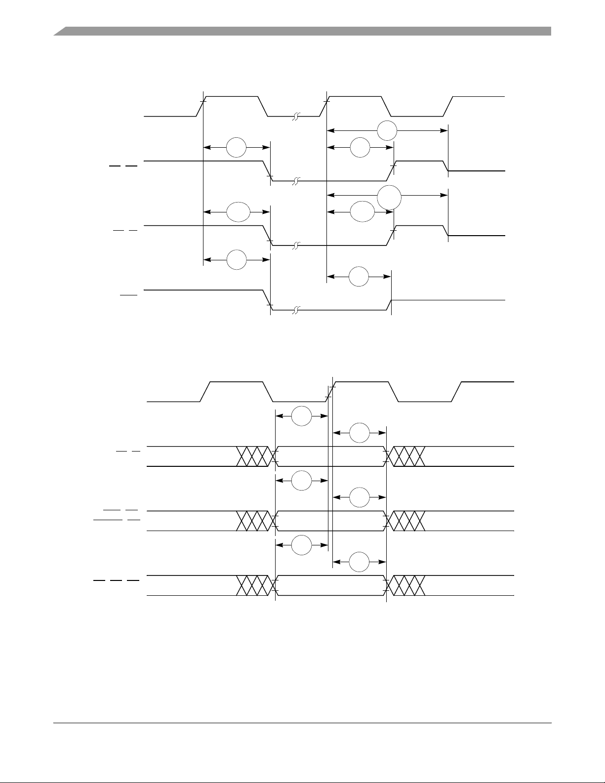
Figure 5 provides the timing for the synchronous active pull-up and open-drain output signals.
CLKOUT
B13
B12B11
TS
, BB
B13a
B11a B12a
TA, BI
B14
B15
TEA
Figure 5. Synchronous Active Pull-Up Resistor and Open-Drain Outputs Signals Timing
Figure 6 provides the timing for the synchronous input signals.
CLKOUT
B16
B17
TA, BI
B16a
B17a
TEA, KR,
, CR
RETRY
B16b
B17
BB, BG, BR
Figure 6. Synchronous Input Signals Timing
Figure 7 provides normal case ti ming for in put dat a. It also appl ies t o normal r ead acc ess es under the con trol o f the
UPM in the memo ry controller.
MPC860 Family Hardware Specifications, Rev. 7
22 Freescale Semiconduct or
Page 23
Bus Signal Timing
CLKOUT
B16
B17
TA
B18
B19
D[0:31],
DP[0:3]
Figure 7. Input Data Timing in Normal Case
Figure 8 provides the timing for the input data controlled by the UPM for data beats where DLT3 = 1 in the UPM
RAM words. (This is only the case where data is latched on the falling edge of CLKOUT.)
CLKOUT
TA
B20
B21
D[0:31],
DP[0:3]
Figure 8. Input Data Timing when Controlled by UPM in the Memory Controller
and DLT3 = 1
Figure 9 through Figure 12 provide the timing for the external bus read controlled by various GPCM factors.
MPC860 Family Hardware Specifications, Rev. 7
Freescale Semiconduc tor 23
Page 24
Bus Signal Timing
CLKOUT
A[0:31]
B11 B12
TS
B8
CSx
OE
WE[0:3]
D[0:31],
DP[0:3]
B22
B25
B28
B23
B26
B19
B18
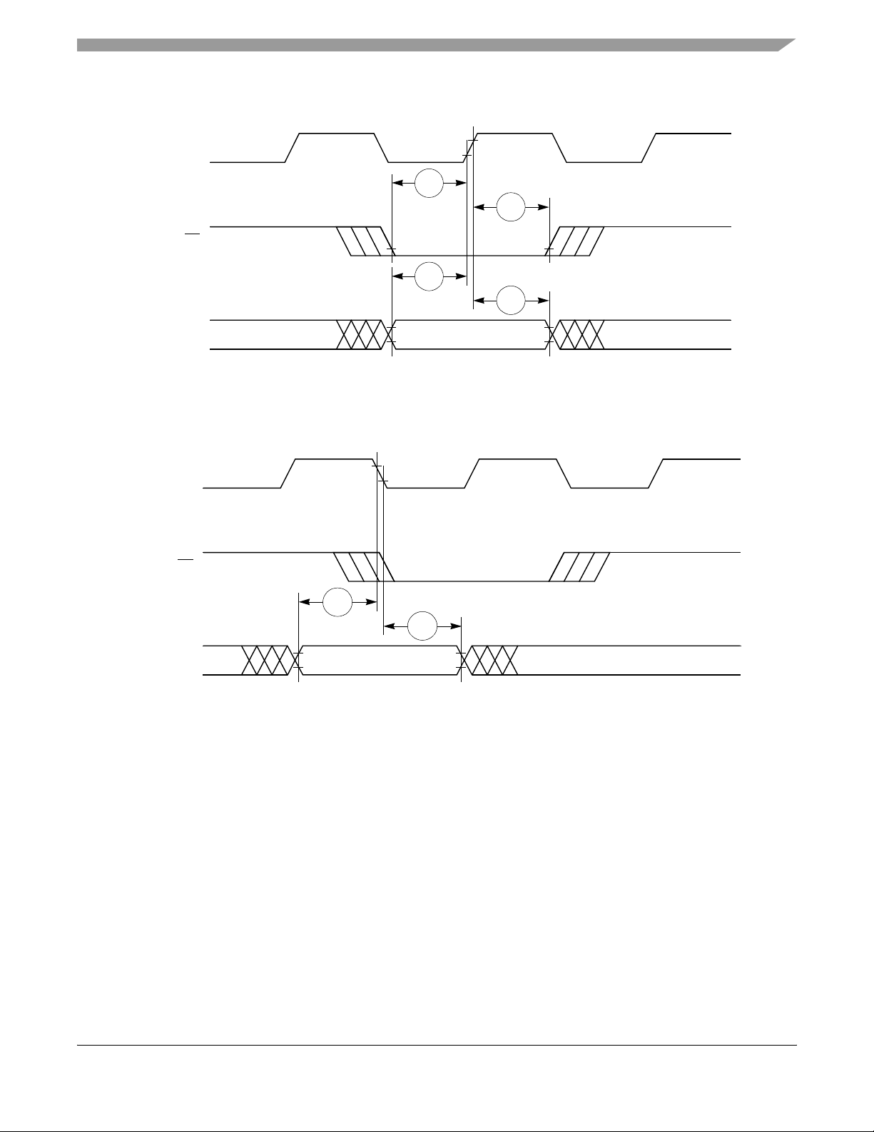
Figure 9. External Bus Read Timing (GPCM Controlled—ACS = 00)
MPC860 Family Hardware Specifications, Rev. 7
24 Freescale Semiconduct or
Page 25

CLKOUT
TS
A[0:31]
Bus Signal Timing
B11 B12
B8
B22a
B23
CSx
B25B24
B26
OE
B19B18
D[0:31],
DP[0:3]
Figure 10. External Bus Read Timing (GPCM Controlled—TRLX = 0, ACS = 10)
CLKOUT
B11 B12
TS
B22bB8
A[0:31]
B22c B23
CSx
B24a B25 B26
OE
B19B18
D[0:31],
DP[0:3]
Figure 11. External Bus Read Timing (GPCM Controlled—TRLX = 0, ACS = 11)
MPC860 Family Hardware Specifications, Rev. 7
Freescale Semiconduc tor 25
Page 26

Bus Signal Timing
CLKOUT
A[0:31]
B11 B12
TS
B8
B22a
B23
CSx
OE
B27
B27a
B22bB22c B19B18
B26
D[0:31],
DP[0:3]
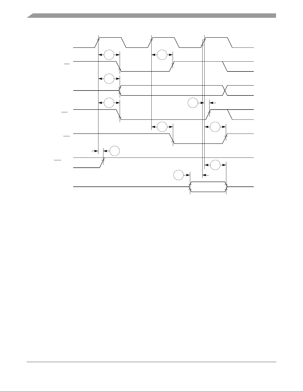
Figure 12. External Bus Read Timing (GPCM Controlled—TRLX = 0 or 1, ACS = 10, ACS = 11)
Figure 13 through Figure 15 provide the timin g for the exte rnal bus write controlled by various GPCM factors.
MPC860 Family Hardware Specifications, Rev. 7
26 Freescale Semiconduct or
Page 27

C
LKOUT
Bus Signal Timing
TS
A[0:31]
CSx
WE[0:3]
OE
D[0:31],
DP[0:3]
B11
B12
B8
B22 B23
B26
B8 B9
B30
B28B25
B29b
B29
Figure 13. External Bus Write Timing (GPCM Controlled—TRLX = 0 or 1, CSNT = 0)
MPC860 Family Hardware Specifications, Rev. 7
Freescale Semiconduc tor 27
Page 28

Bus Signal Timing
CLKOUT
TS
A[0:31]
CSx
WE[0:3]
OE
D[0:31],
DP[0:3]
B11
B8
B22
B26
B8
B12
B28bB28d
B25
B28aB9B28c
B30aB30c
B23
B29c B29g
B29aB29f
Figure 14. External Bus Write Timing (GPCM Controlled—TRLX = 0 or 1, CSNT = 1)
MPC860 Family Hardware Specifications, Rev. 7
28 Freescale Semiconduct or
Page 29

C
LKOUT
TS
Bus Signal Timing
B12B11
B8
A[0:31]
B28b B28d
CSx
B25 B29eB29i
WE[0:3]
B26 B29dB29h
OE
B28aB28c B9B8
D[0:31],
DP[0:3]
Figure 15. External Bus Write Timing (GPCM Controlled—TRLX = 0 or 1, CSNT = 1)
Figure 16 provides the timing for the external bus controlled by the UPM.
B30dB30b
B23B22
B29b
MPC860 Family Hardware Specifications, Rev. 7
Freescale Semiconduc tor 29
Page 30

Bus Signal Timing
CLKOUT
A[0:31]
BS_A
BS_B
CSx
[0:3],
[0:3]
B8
B34
B34b
B31
B34a
B32
B31a
B31d
B32aB32d
B31c
B31b
B32c
B32b
B36
B35
B35a
B35b
B33a
B33
GPL_A[0:5],
[0:5]
GPL_B
Figure 16. External Bus Timing (UPM Controlled Signals)
Figure 17 provides the timing for the asynchronous asserted UPWAIT signal controlled by the UPM.
MPC860 Family Hardware Specifications, Rev. 7
30 Freescale Semiconduct or
Page 31

Bus Signal Timing
CLKOUT
B37
UPWAIT
B38
CSx
BS_A[0:3],
[0:3]
BS_B
GPL_A
[0:5],
GPL_B
[0:5]
Figure 17. Asynchronous UPWAIT Asserted Detection in UPM Handled Cycles Timing
Figure 18 provides the timing for the asynchronous negated UPWAIT signal controlled by the UPM.
CLKOUT
B37
UPWAIT
B38
CSx
BS_A[0:3],
BS_B
[0:3]
GPL_A[0:5],
[0:5]
GPL_B
Figure 18. Asynchronous UPWAIT Negated Detection in UPM Handled Cycles Timing
Figure 19 provides the timing for the synchronous external master access controlled by the GPCM.
MPC860 Family Hardware Specifications, Rev. 7
Freescale Semiconduc tor 31
Page 32

Bus Signal Timing
C
CLKOUT
B41 B42
TS
B40
A[0:31],
TSIZ[0:1],
, BURST
R/W
B22
CSx
Figure 19. Synchronous External Master Access Timing (GPCM Handled ACS = 00)
Figure 20 provides the timing for the asynchronous external master memory access controlled by the GPCM.
CLKOUT
B39
AS
B40
A[0:31],
TSIZ[0:1],
R/W
B22
CSx
Figure 20. Asynchronous External Master Memory Access Timing
(GPCM Controlled—ACS = 00)
Figure 21 provides the timing for the asynchronous external master control signals negation.
AS
B43
Sx, WE[0:3],
, GPLx,
OE
BS[0:3]
Figure 21. Asynchronous External Master—Control Signals Negation Timing
MPC860 Family Hardware Specifications, Rev. 7
32 Freescale Semiconduct or
Page 33

Table 8 provides interrupt timing for the MPC860.
Table 8. Interrupt Timing
Bus Signal Timing
Num Characteristic
I39 IRQx valid to CLKOUT rising edge (setup time) 6.00 — ns
I40 IRQx hold time after CLKOUT 2.00 — ns
I41 IRQx pulse width low 3.00 — ns
I42 IRQx pulse width high 3.00 — ns
I43 IRQx edge-to-edge time 4 × T
1
The timings I39 and I40 des cribe the test ing condi tions u nder whic h the IRQ line s ar e tested when bei ng de fined a s
level-sensitive. The
to the CLKOUT.
The timings I41, I42, and I43 are specified to allow the correct function of the IRQ lines detection circuitry and have
no direct relation with the total system interrupt latency that the MPC860 is able to support.
IRQ lines are synchronized interna lly and do no t hav e to be ass ert ed or n egated with reference
1
All Frequencies
Min Max
CLOCKOUT
— —
Figure 22 provides the interrupt detection timing for the external level-sensitive lines.
CLKOUT
I39
I40
Unit
x
IRQ
Figure 22. Interrupt Detection Timing for External Level Sensitive Lines
Figure 23 provides the interrupt d etection timing for the external edge-sensitive lines.
CLKOUT
I41 I42
IRQx
I43
I43
Figure 23. Interrupt Detection Timing for Exter nal Edge Sensitive Lines
MPC860 Family Hardware Specifications, Rev. 7
Freescale Semiconduc tor 33
Page 34

Bus Signal Timing
Table 9 shows the PCMCIA timing for the MPC860.
Table 9. PCMCIA Timing
33 MHz 40 MHz 50 MHz 66 MHz
Num Characteristic
Min Max Min Max Min Max Min Max
Unit
P44 A(0:31), REG valid to PCMCIA
Strobe asserted
P45 A(0:31), REG valid to ALE negation 128.30 — 23.00 — 18.00 — 13.15 — ns
P46 CLKOUT to REG valid 7.58 15.58 6.25 14.25 5.00 13.00 3.79 11.84 ns
P47 CLKOUT to REG invalid 8.58 — 7.25 — 6.00 — 4.84 — ns
P48 CLKOUT to CE1, CE2 asserted 7.58 15.58 6.25 14.25 5.00 13.00 3.79 11.84 ns
P49 CLKOUT to CE1, CE2 negated 7.58 15.58 6.25 14.25 5.00 13.00 3.79 11.84 ns
P50 CLKOUT to PCOE, IORD, PCWE,
IOWR assert time
P51 CLKOUT to PCOE, IORD, PCWE,
IOWR negate time
P52 CLKOUT to ALE assert time 7.58 15.58 6.25 14.25 5.00 13.00 3.79 10.04 ns
P53 CLKOUT to ALE negate time — 15.58 14.25 — 13.00 — 11.84 ns
P54 PCWE, IOWR negated to D(0:31)
P55 WAITA and WAITB valid to CLKOUT
P56 CLKOUT rising edge to WAITA and
1
PSST = 1. Otherwise add PSST times cycle time.
PSHT = 0. Otherwise add PSHT times cycle time.
1
invalid
rising edge
WAITB invalid
1
1
1
20.73 — 16.75 — 13.00 — 9.36 — ns
— 11.00 11.00 — 11.00 — 11.00 ns
2.00 11.00 2.00 11.00 2.00 11.00 2.00 11.00 ns
5.58 — 4.25 — 3.00 — 1.79 — ns
8.00 — 8.00 — 8.00 — 8.00 — ns
2.00 — 2.00 — 2.00 — 2.00 — ns
These synchronous timings define when the WAITx signals are detected in order to freeze (or relieve) the
PCMCIA current cycle. The
WAITx assertion will be effective only if it is detected 2 cycles be fore the PSL
timer expiration. See Chapter 16, “PC M CIA Interface,” in the MPC860 PowerQUICC User’s Manual.
Figure 24 provides the PCMCIA access cycle timing for the external bus read.
MPC860 Family Hardware Specifications, Rev. 7
34 Freescale Semiconduct or
Page 35

CLKOUT
TS
A[0:31]
Bus Signal Timing
P44
P46 P45
REG
P48 P49
CE1/CE2
PCOE, IORD
P53P52 P52
ALE
D[0:31]
Figure 24. PCMCIA Access Cycle Timing External Bus Read
Figure 25 provides the PCMCIA access cycle timing for the external bus write.
P47
P51P50
B19B18
MPC860 Family Hardware Specifications, Rev. 7
Freescale Semiconduc tor 35
Page 36

Bus Signal Timing
P
CLKOUT
A[0:31]
TS
P44
P46 P45
REG
P48 P49
CE1/CE2
CWE, IOWR
ALE
D[0:31]
Figure 25. PCMCIA Access Cycle Timing External Bus Write
Figure 26 provides the PCMCIA WAIT signal detection timing.
P47
P51P50
P53P52 P52
B9B8
P54
CLKOUT
P55
P56
WAITx
Figure 26. PCMCIA WAIT Signal Detection Timing
Table 10 shows the PCMCIA port timing for the MPC860.
MPC860 Family Hardware Specifications, Rev. 7
36 Freescale Semiconduct or
Page 37

Bus Signal Timing
Table 10. PCMCIA Port Timing
33 MHz 40 MHz 50 MHz 66 MHz
Num Characteristic
Min Max Min Max Min Max Min Max
P57 CLKOUT to OPx valid — 19.00 — 19.00 — 19.00 — 19.00 ns
P58 HRESET negated to OPx drive
P59 IP_Xx valid to CLKOUT rising edge 5.00 — 5.00 — 5.00 — 5.00 — ns
1
25.73 — 21.75 — 18.00 — 14.36 — ns
Unit
P60 CLKOUT rising edge to IP_Xx
invalid
1
OP2 and OP3 only
1.00 — 1.00 — 1.00 — 1.00 — ns
Figure 27 provides the PCMCIA output port timing for the MPC860.
CLKOUT
P57
Output
Signals
HRESET
P58
OP2, OP3
Figure 27. PCMCIA Output Port Timing
Figure 28 provides the PCMCIA output port timing for the MPC860.
CLKOUT
P59
P60
Input
Signals
Figure 28. PCMCIA Input Port Timing
Table 11 shows the debug port timing for the MPC860.
MPC860 Family Hardware Specifications, Rev. 7
Freescale Semiconduc tor 37
Page 38

Bus Signal Timing
Num Characteristic
Table 11. Debug Port Timing
All Frequencies
Unit
Min Max
P61 DSCK cy cle time 3 × T
P62 DSCK clock pulse width 1.25 × T
P63 DSCK rise and fall times 0.00 3.00 ns
P64 DSDI input data setup time 8.00 — ns
P65 DSDI data hold time 5.00 — ns
P66 DSCK low to DSDO data valid 0.00 15.00 ns
P67 DSCK low to DSDO invalid 0.00 2.00 ns
CLOCKOUT
CLOCKOUT
— —
— —
Figure 29 provides the input timing for the debug port clock.
DSCK
D61
D61
D63
D62
D62
D63
Figure 29. Debug Port Clock Input Timing
Figure 30 provides the timing for the debug port.
DSCK
DSDI
DSDO
D64
D65
D66
D67
Figure 30. Debug Port Timings
MPC860 Family Hardware Specifications, Rev. 7
38 Freescale Semiconduct or
Page 39

Table 12 shows the reset timing for the MPC860.
Table 12. Reset Timing
Num Characteristic
Min Max Min Max Min Max Min Max
Bus Signal Timing
33 MHz 40 MHz 50 MHz 66 MHz
Unit
R69 CLKOUT to HRESET high
impedance
R70 CLKOUT to SRESET high
impedance
R71 RSTCONF pulse width 515.15— 425.0
R72 — — — — — — — — —
R73 Configuration data to HRESET rising
edge setup time
R74 Configuration data to RSTCONF
rising edge setup time
R75 Configuration data hold time after
RSTCONF negation
R76 Configuration data hold time after
HRESET negation
R77 HRESET and RSTCONF asserted to
data out drive
R78 RSTCONF negated to data out high
impedance
R79 CLKOUT of last rising edge before
chip three-state
high impedance
HRESET to data out
— 20.00 — 20.00 — 20.00 — 20.00 ns
— 20.00 — 20.00 — 20.00 — 20.00 ns
340.00— 257.58— ns
0
504.55— 425.00— 350.00— 277.27— ns
350.00— 350.00— 350.00— 350.00— ns
0.00 — 0.00 — 0.00 — 0.00 — ns
0.00 — 0.00 — 0.00 — 0.00 — ns
— 25.00 25.00 — 25.00 — 25.00 ns
— 25.00 — 25.00 — 25.00 — 25.00 ns
— 25.00 — 25.00 — 25.00 — 25.00 ns
R80 DSDI, DSCK setup 90.91 — 75.00 — 60.00 — 45.45 — ns
R81 DSDI, DSCK hold time 0.00 — 0.00 — 0.00 — 0.00 — ns
R82 SRESET negated to CLKOUT rising
edge for DSDI and DSCK sample
242.42— 200.00— 160.00— 121.21— ns
Figure 31 shows the reset timing for the data bus configuration.
MPC860 Family Hardware Specifications, Rev. 7
Freescale Semiconduc tor 39
Page 40

Bus Signal Timing
HRESET
R71
R76
RSTCONF
R73
R74
D[0:31] (IN)
R75
Figure 31. Reset Timing—Configuration from Data Bus
Figure 32 provides the reset timing for the data bus weak drive during configuration.
CLKOUT
R69
HRESET
RSTCONF
R77 R78
D[0:31] (OUT)
(Weak)
Figure 32. Reset Timing—Data Bus Weak Drive During Configuration
Figure 33 provides the reset timing for the debug port configuration.
R79
MPC860 Family Hardware Specifications, Rev. 7
40 Freescale Semiconduct or
Page 41

IEEE 1149.1 Electrical Specifications
CLKOUT
R70
R82
SRESET
R80R80
R81
DSCK, DSDI
R81
Figure 33. Reset Timing—Debug Port Configuration
10 IEEE 1149.1 Electrical Specifications
Table 13 provides the JTAG timings for the MPC860 shown in Figure 34 through Figure 37.
Table 13. JTAG Timin g
All Frequencies
Num Characteristic
Min Max
J82 TCK cycle time 100.00 — ns
J83 TCK clock pulse width measured at 1.5 V 40.00 — ns
J84 TCK rise and fall times 0.00 10.00 ns
J85 TMS, TDI data setup time 5.00 — ns
J86 TMS, TDI data hold time 25.00 — ns
J87 TCK low to TDO data valid — 27.00 ns
J88 TCK low to TDO data invalid 0.00 — ns
J89 TCK low to TDO high impedance — 20.00 ns
J90 TRST assert time 100.00 — ns
J91 TRST setup time to TCK low 40.00 — ns
J92 TCK falling edge to output valid — 50.00 ns
J93 TCK falling edge to output valid out of high impedance — 50.00 ns
J94 TCK falling edge to output high impedance — 50.00 ns
Unit
J95 Boundary scan input valid to TCK rising edge 50.00 — ns
J96 TCK rising edge to boundary scan input invalid 50.00 — ns
MPC860 Family Hardware Specifications, Rev. 7
Freescale Semiconduc tor 41
Page 42

IEEE 1149.1 Electrical Specifications
TCK
TCK
TMS, TDI
TDO
J82 J83
J82 J83
J84 J84
Figure 34. JTAG Test Clock Input Timing
J85
J86
J87
J88 J89
TCK
TRST
TCK
Output
Signals
Output
Signals
Figure 35. JTAG Test Access Port Timing Diagram
J91
J90
Figure 36. JTAG TRST Timing Diagram
J92 J94
J93
J95 J96
Output
Signals
Figure 37. Boundary Scan (JTAG) Timing Diagram
MPC860 Family Hardware Specifications, Rev. 7
42 Freescale Semiconduct or
Page 43

CPM Electrical Characteristics
11 CPM Electrical Characteristics
This section pr ovi des t he AC and DC electric al specifications f or the communications processor module (CPM ) of
the MPC860.
11.1 PIP/PIO AC Electrical Specifications
Table 14 provides the PIP/PIO AC timings as shown in Figure 38 through Figure 42.
Table 14. PIP/PIO Timing
All Frequencies
Num Characteristic
Min Max
21 Data-in setup time to STBI low 0 — ns
22 Data-in hold time to STBI high 2.5 – t3
23 STBI pulse width 1.5 — CLK
24 STBO pulse width 1 CLK – 5 ns — ns
25 Data-out setup time to STBO low 2 — CLK
1
— CLK
Unit
26 Data-out hold time from STBO high 5 — CLK
27 STBI low to STBO low (Rx interlock) — 2 CLK
28 STBI low to STBO high (Tx interlock) 2 — CLK
29 Data-in setup time to clock high 15 — ns
30 Data-in hold time from clock high 7.5 — ns
31 Clock low to data-out valid (CPU writes data, control, or direction) — 25 ns
1
t3 = Specification 23.
DATA-IN
21
23
STBI
27
24
STBO
22
Figure 38. PIP Rx (Interlock Mode) Timing Diagram
MPC860 Family Hardware Specifications, Rev. 7
Freescale Semiconduc tor 43
Page 44

CPM Electrical Characteristics
DATA-OUT
STBO
(Output)
STBI
(Input)
DATA-IN
STBI
(Input)
25
24
28
23
26
Figure 39. PIP Tx (Interlock Mode) Timing Diagram
2221
23
STBO
(Output)
DATA-OUT
STBO
(Output)
STBI
(Input)
24
Figure 40. PIP Rx (Pulse Mode) Timing Diagram
2625
24
23
Figure 41. PIP TX (Pulse Mode) Timing Diagram
MPC860 Family Hardware Specifications, Rev. 7
44 Freescale Semiconduct or
Page 45

CLKO
29
30
DATA-IN
31
DATA-OUT
Figure 42. Parallel I/O Data-In/Data-Out Timing Diagram
11 .2 Port C Interrupt AC Electrical Specifications
Table 15 provides the timings for port C interrupts.
Table 15. Port C Interrupt Timing
CPM Electrical Characteristics
≥ 33.34 MHz
Num Characteristic
Min Max
35 Port C interrupt pulse width low (edge-triggered mode) 55 — ns
36 Port C interrupt minimum time between active edges 55 — ns
1
External bus frequency of greater than or equal to 33.34 MHz.
Figure 43 shows the port C interrupt detection timing.
36
Port C
(Input)
35
Figure 43. Port C Interrupt Detection Timing
11.3 IDMA Controller AC Electrical Specifications
Table 16 provides the IDMA controller timings as shown in Figure 44 through Figure 47.
1
Unit
MPC860 Family Hardware Specifications, Rev. 7
Freescale Semiconduc tor 45
Page 46

CPM Electrical Characteristics
Num Characteristic
40 DREQ setup time to clock high 7 — ns
41 DREQ hold time from clock high 3 — ns
42 SDACK assertion delay from clock high — 12 ns
43 SDACK negation delay from clock low — 12 ns
44 SDACK negation de lay from TA low — 20 ns
45 SDACK negation delay from clock high — 15 ns
Table 16. IDMA Controller Timing
All Frequencies
Unit
Min Max
46 TA assertion to falling edge of the clock setup time (applies to
external TA)
CLKO
(Output)
40
DREQ
(Input)
Figure 44. IDMA External Requests Timing Diagram
7 — ns
41
MPC860 Family Hardware Specifications, Rev. 7
46 Freescale Semiconduct or
Page 47

CLKO
(Output)
TS
(Output)
R/W
(Output)
CPM Electrical Characteristics
42
DATA
TA
(Input)
SDACK
43
46
Figure 45. SDACK Timing Diagram—Peripheral Write, Externally-Generated TA
CLKO
(Output)
TS
(Output)
R/W
(Output)
42 44
DATA
TA
(Output)
SDACK
Figure 46. SDACK Timing Diagram—Peripheral Write, Internally-Generated TA
MPC860 Family Hardware Specifications, Rev. 7
Freescale Semiconduc tor 47
Page 48

CPM Electrical Characteristics
CLKO
(Output)
TS
(Output)
R/W
(Output)
DATA
TA
(Output)
SDACK
42 45
Figure 47. SDACK Timing Diagram—Peripheral Read, Internally-Generated TA
11.4 Baud Rate Generator AC Electrical Specifications
Table 17 provides the baud rate generator timings as shown in Figure 48.
Table 17. Baud Rate Generator Timing
All Frequencies
Num Characteristic
Min Max
50 BRGO rise and fall time — 10 ns
51 BRGO duty cycle 40 60 %
52 BRGO cycle 40 — ns
50
BRGOX
51
52
50
51
Unit
Figure 48. Baud Rate Generator Timing Diagram
MPC860 Family Hardware Specifications, Rev. 7
48 Freescale Semiconduct or
Page 49

11.5 Timer AC Electrical Specifications
Table 18 provides the general-purpose timer timings as shown in Figure 49.
Num Characteristic
61 TIN/TGATE rise and fall time 10 — ns
62 TIN/TGATE low time 1 — CLK
63 TIN/TGATE high time 2 — CLK
64 TIN/TGATE cycle time 3 — CLK
65 CLKO low to TOUT valid 3 25 ns
CLKO
Table 18. Timer Timin g
60
CPM Electrical Characteristics
All Frequencies
Unit
Min Max
626361
TIN/TGATE
(Input)
61
65
TOUT
(Output)
64
Figure 49. CPM General-Purpose Timers Timing Diagram
11.6 Serial Interface AC Electrical Specifications
Table 19 provides the serial interface timings as shown in Figure 50 through Figure 54.
Table 19. SI Timing
All Frequencies
Num Characteristic
Min Max
70 L1RCLK, L1TCLK frequency (DSC = 0)
71 L1RCLK, L1TCLK width low (DSC = 0)
71a L1RCLK, L1TCLK wid th high (D SC = 0)
72 L1TXD, L1S T(1–4), L1RQ, L1CLKO rise/fall time — 15.00 ns
1, 2
— SYNCCLK/2.5 MHz
2
3
P + 10 — ns
P + 10 — ns
Unit
73 L1RSYNC, L1TSYNC valid to L1CLK edge (SYNC setup time) 20.00 — ns
74 L1CLK edge to L1RSYNC, L1TSYNC, invalid (SYNC hold time) 35.00 — ns
MPC860 Family Hardware Specifications, Rev. 7
Freescale Semiconduc tor 49
Page 50

CPM Electrical Characteristics
Table 19. SI Timing (continued)
All Frequencies
Num Characteristic
Min Max
75 L1RSYNC, L 1TSYNC rise/fall time — 15.00 ns
76 L1RXD valid to L1CLK edge (L1RXD setup time) 17.00 — ns
77 L1CLK edge to L1RXD invalid (L1RXD hold time) 13.00 — ns
78 L1CLK edge to L1ST(1–4) valid
78A L1SYNC valid to L1ST(1–4) valid 10.00 45.00 ns
79 L1CLK edge to L1ST(1–4) invalid 10.00 45.00 ns
80 L1CLK edge to L1TXD valid 10.00 55.00 ns
80A L1TSYNC valid to L1TXD valid
81 L1CLK edge to L1TXD high impedance 0.00 42.00 ns
4
4
10.00 45.00 ns
10.00 55.00 ns
Unit
82 L1RCLK, L1TCLK frequency (DSC =1) — 16.00 or
SYNCCLK/2
83 L1RCLK, L1TCLK width low (DSC =1) P + 10 — ns
83a L1RCLK, L1TCLK wid th high (D SC = 1)
3
P + 10 — ns
84 L1CLK edge to L 1CLKO valid (DSC = 1) — 30.00 ns
85 L1RQ valid before falling edge of L1TSYNC
86 L1GR setup time
2
4
1.00 — L1TCL
42.00 — ns
87 L1GR hold time 42.00 — ns
88 L1CLK edge to L1SYNC valid (FSD = 00) CNT = 0000, BYT = 0,
— 0.00 ns
DSC = 0)
1
The ratio SYNCCLK/L1RCLK must be greater than 2.5/1.
2
These specs are valid for IDL mode only.
3
Where P = 1/CLKOUT. Thus, for a 25-MHz CLKO1 rate, P = 40 ns.
4
These strobes and TxD on the first bit of the frame become valid after L1CLK edge or L1SYNC, whichever comes
later.
MHz
K
MPC860 Family Hardware Specifications, Rev. 7
50 Freescale Semiconduct or
Page 51

L1RCLK
(FE=0, CE=0)
(Input)
L1RCLK
(FE=1, CE=1)
(Input)
L1RSYNC
(Input)
73
71
CPM Electrical Characteristics
70 71a
72
RFSD=1
75
74 77
L1RXD
(Input)
L1ST(4-1)
(Output)
BIT0
76
78
79
Figure 50. SI Re ceive Timing Diag ram with Normal Clocking (DSC = 0)
MPC860 Family Hardware Specifications, Rev. 7
Freescale Semiconduc tor 51
Page 52

CPM Electrical Characteristics
L1RCLK
(FE=1, CE=1)
(Input)
82
L1RCLK
(FE=0, CE=0)
(Input)
L1RSYNC
(Input)
72
RFSD=1
75
73
74 77
83a
L1RXD
(Input)
L1ST(4-1)
(Output)
L1CLKO
(Output)
BIT0
76
78
84
79
Figure 51. SI Receive Timing with Double-Speed Clocking (DSC = 1)
MPC860 Family Hardware Specifications, Rev. 7
52 Freescale Semiconduct or
Page 53

L1TCLK
(FE=0, CE=0)
(Input)
L1TCLK
(FE=1, CE=1)
(Input)
L1TSYNC
(Input)
73
71 70
72
TFSD=0
75
74
80a
CPM Electrical Characteristics
81
L1TXD
(Output)
L1ST(4-1)
(Output)
BIT0
80
78
Figure 52. SI Transmit Timing Diagram (DSC = 0)
79
MPC860 Family Hardware Specifications, Rev. 7
Freescale Semiconduc tor 53
Page 54

CPM Electrical Characteristics
L1RCLK
(FE=0, CE=0)
(Input)
L1RCLK
(FE=1, CE=1)
(Input)
L1RSYNC
(Input)
73
75
74
72
82
TFSD=0
83a
81
L1TXD
(Output)
L1ST(4-1)
(Output)
L1CLKO
(Output)
BIT0
80
78a
78
84
79
Figure 53. SI Transmit Timing with Double Speed Clocking (DSC = 1)
MPC860 Family Hardware Specifications, Rev. 7
54 Freescale Semiconduct or
Page 55

81
CPM Electrical Characteristics
78
87
71
73
12345678910 11 12 13 14 15 16 17 18 19 20
(Input)
L1RCLK
71
74
80
(Input)
L1RSYNC
72
76
77
B17 B16 B14 B13 B12 B11 B10 D1 A B27 B26 B25 B24 B23 B22 B21 B20 D2 MB15
(Input)
L1RXD
L1ST(4-1)
(Output)
B17 B16 B15 B14 B13 B12 B11 B10 D1 A B27 B26 B25 B24 B23 B22 B21 B20 D2 M
L1TXD
(Output)
85
86
L1RQ
(Output)
L1GR
(Input)
Figure 54. IDL Timing
MPC860 Family Hardware Specifications, Rev. 7
Freescale Semiconduc tor 55
Page 56

CPM Electrical Characteristics
11.7 SCC in NMSI Mode Electrical Specifications
Table 20 provides the NMSI external clock timing.
Table 20. NMSI External Clock Timing
All Frequencies
Num Characteristic
Min Max
100 RCLK1 and TCLK1 width high
101 RCLK1 and TCLK1 width low 1/SYNCCLK + 5 — ns
102 RCLK1 and TCLK1 rise/fall time — 15.00 ns
103 TXD1 active delay (from TCLK1 falling edge) 0.00 50.00 ns
104 RTS1 active/inactive delay (from TCLK1 falling edge) 0.00 50.00 ns
105 CTS1 setup time to TCLK1 rising edge 5.00 — ns
106 RXD1 setup time to RCLK1 rising edge 5.00 — ns
107 RXD1 hold time from RCLK1 rising edge
108 CD1 setup Time to RCLK1 rising edge 5.00 — ns
1
The ratios SYNCCLK/RCLK1 and SYNCCLK/TCLK1 must be greater than or equal to 2.25/1.
2
Also applies to CD and CTS hold time when they are us ed as external sync signals.
1
2
1/SYNCCLK — ns
5.00 — ns
Unit
Table 21 provides the NMSI internal clock timing.
Table 21. NMSI Internal Clock Timing
All Frequencies
Num Characteristic
Min Max
100 RCLK1 and TCLK1 frequency
102 RCLK1 and TCLK1 rise/fall time — — ns
103 TXD1 active delay (from TCLK1 falling edge) 0.00 30.00 ns
104 RTS1 active/inactive delay (from TCLK1 falling edge) 0.00 30.00 ns
105 CTS1 setup time to TCLK1 rising edge 40.00 — ns
106 RXD1 setup time to RCLK1 rising edge 40.00 — ns
107 RXD1 hold time from RCLK1 rising edge
108 CD1 setup time to RCLK1 rising edge 40.00 — ns
1
The ratios SYNCCLK/RCLK1 and SYNCCLK/TCLK1 must be greater than or equal to 3/1.
2
Also applies to CD and CTS hold time when they are us ed as external sync signals.
1
2
0.00 SYNCCLK/3 MHz
0.00 — ns
Figure 55 through Figure 57 show the NMSI timings.
Unit
MPC860 Family Hardware Specifications, Rev. 7
56 Freescale Semiconduct or
Page 57

RCLK1
CPM Electrical Characteristics
RxD1
(Input)
CD1
(Input)
CD1
(SYNC Input)
TCLK1
106
102
102 101
100
107
Figure 55. SCC NMSI Receive Timing Diagram
102
102 101
100
108
107
TxD1
(Output)
RTS1
(Output)
CTS1
(Input)
CTS1
(SYNC Input)
103
105
104
Figure 56. SCC NMSI Transmit Timing Diagram
104
107
MPC860 Family Hardware Specifications, Rev. 7
Freescale Semiconduc tor 57
Page 58

CPM Electrical Characteristics
TCLK1
102
TxD1
(Output)
RTS1
(Output)
CTS1
(Echo Input)
102 101
100
103
104
105
Figure 57. HDLC Bus Timing Diagram
11.8 Ethernet Electrical Specifications
Table 22 provides the Ethernet timings as shown in Figure 58 through Figure 62.
Table 22. Ethernet Timing
104107
All Frequencies
Num Characteristic
Min Max
120 CLSN width high 40 — ns
121 RCLK1 rise/fall time — 15 ns
122 RCLK1 width low 40 — ns
123 RCLK1 clock period
124 RXD1 setup time 20 — ns
125 RXD1 hold time 5 — ns
126 RENA active delay (from RCLK1 rising edge of the last data bit) 10 — ns
127 RENA width low 100 — ns
128 TCLK1 rise/fall time — 15 ns
129 TCLK1 width low 40 — ns
130 TCLK1 clock period
131 TXD1 active delay (fr om TCLK1 rising edge) 10 50 ns
132 TXD1 ina c tive delay (from TCLK1 risi ng edge) 10 50 ns
133 TENA active delay (from TCLK1 rising edge) 10 50 ns
1
1
80 120 ns
99 101 ns
Unit
MPC860 Family Hardware Specifications, Rev. 7
58 Freescale Semiconduct or
Page 59

CPM Electrical Characteristics
Table 22. Ethernet Timing (continued)
All Frequencies
Num Characteristic
Min Max
134 TENA inactive delay (from TCLK1 rising edge) 10 50 ns
135 RSTRT active delay (from TCLK1 falling edge) 10 50 ns
136 RSTRT inactive delay (from TCLK1 falling edge) 10 50 ns
137 REJECT width low 1 — CLK
138 CLKO1 low to SDACK asserted
139 CLKO1 low to SDACK negated
1
The ratios SYNCCLK/RCLK1 and SYNCCLK/TCLK1 must be greater than or equal to 2/1.
2
SDACK is asserted whenever the SDMA writes the incoming frame DA into memory.
CLSN(CTS1)
(Input)
2
2
— 20 ns
— 20 ns
120
Unit
RCLK1
RxD1
(Input)
RENA(CD1)
(Input)
Figure 58. Ethernet Collision Timing Diagram
121
124 123
125
121
126
Figure 59. Ethernet Receive Timing Diagram
Last Bit
127
MPC860 Family Hardware Specifications, Rev. 7
Freescale Semiconduc tor 59
Page 60

CPM Electrical Characteristics
TCLK1
128
128
131 121
TxD1
(Output)
132
133 134
TENA(RTS1)
(Input)
RENA(CD1)
(Input)
(NOTE 2)
NOTES:
Transmit clock invert (TCI) bit in GSMR is set.
1.
If RENA is deasserted before TENA, or RENA is not asserted at all during transmit, then the
2.
CSL bit is set in the buffer descriptor at the end of the frame transmission.
Figure 60. Ethernet Transmit Timing Diagram
RCLK1
129
RxD1
(Input)
RSTRT
(Output)
REJECT
0
1 1 BIT1 BIT2
Start Frame De-
125
Figure 61. CAM Interface Receive Start Timing Diagram
137
Figure 62. CAM Interface REJECT Timing Diagram
MPC860 Family Hardware Specifications, Rev. 7
136
60 Freescale Semiconduct or
Page 61

CPM Electrical Characteristics
11.9 SMC Transparent AC Electrical Specifications
Table 23 provides the SMC transparent timings as shown in Figure 63.
Table 23. SMC Transparent Timing
All Frequencies
Num Characteristic
Min Max
150 SMCLK clock period
151 SMCLK width low 50 — ns
151A SMCLK width high 50 — ns
152 SMCLK rise/fall time — 15 ns
153 SMTXD active delay (from SMCLK falling edge) 10 50 ns
154 SMRXD/SMSYNC setup time 20 — ns
155 RXD1/SMSYNC hold time 5 — ns
1
SYNCCLK must be at least twice as fast as SMCLK.
1
100 — ns
Unit
SMCLK
152
SMTXD
(Output)
SMSYNC
SMRXD
(Input)
NOTE:
This delay is equal to an integer number of character-length clocks.1.
152 151
NOTE
154 153
155
154
155
151
150
Figure 63. SMC Transparent Timing Diagram
11.10SPI Master AC Electrical Specifications
Table 24 provides the SPI master timings as shown in Figure 64 and Figure 65.
MPC860 Family Hardware Specifications, Rev. 7
Freescale Semiconduc tor 61
Page 62

CPM Electrical Characteristics
Num Characteristic
Table 24. SPI Master Timing
All Frequencies
Unit
Min Max
160 MASTER cycle time 4 1024 t
161 MASTER clock (SCK) high or low time 2 512 t
cyc
cyc
162 MASTER data setup time (inputs) 50 — ns
163 Master data hold time (inputs) 0 — ns
164 Master data valid (after SCK edge) — 20 ns
165 Master data hold time (outputs) 0 — ns
166 Rise time output — 15 ns
167 Fall time output — 15 ns
SPICLK
(CI=0)
(Output)
166167161
161 160
SPICLK
(CI=1)
(Output)
163
162
166
167
SPIMISO
(Input)
SPIMOSI
(Output)
msb Data lsb msb
165 164
167 166
msb lsb msb
Data
Figure 64. SPI Master (CP = 0) Timing Diagram
MPC860 Family Hardware Specifications, Rev. 7
62 Freescale Semiconduct or
Page 63

SPICLK
(CI=0)
(Output)
SPICLK
(CI=1)
(Output)
161 160
163
162
CPM Electrical Characteristics
166167161
167
166
SPIMISO
(Input)
SPIMOSI
(Output)
msb Data lsb msb
165 164
167 166
msb lsb msb
Data
Figure 65. SPI Master (CP = 1) Timing Diagram
11.11SPI Slave AC Electrical Specifications
Table 25 provides the SPI slave timings as shown in Figure 66 and Figure 67.
Table 25. SPI Slave Timing
All Frequencies
Num Characteristic
Min Max
170 Slave cycle time 2 — t
171 Slave enable lead time 15 — ns
172 Slave enable lag time 15 — ns
Unit
cyc
173 Slave clock (SPICLK) high or low time 1 — t
174 Slave sequential transfer delay (does not require deselect) 1 — t
175 Slave data setup time (inputs) 20 — ns
176 Slave data hold time (inputs) 20 — ns
177 Slave access time — 50 ns
MPC860 Family Hardware Specifications, Rev. 7
Freescale Semiconduc tor 63
cyc
cyc
Page 64

CPM Electrical Characteristics
SPISEL
(Input)
SPICLK
(CI=0)
(Input)
173 170
SPICLK
(CI=1)
(Input)
177 182
180
171172
174
181182173
181
178
SPIMISO
(Output)
SPIMOSI
(Input)
Datamsb lsb msbUndef
175 179
176 182
msb lsb msb
Data
181
Figure 66. SPI Slave (CP = 0) Timing Diagram
MPC860 Family Hardware Specifications, Rev. 7
64 Freescale Semiconduct or
Page 65

S
S
SPISEL
b
b
(Input)
SPICLK
(CI=0)
(Input)
SPICLK
(CI=1)
(Input)
171 170
173
173
177 182
181
180
CPM Electrical Characteristics
172
174
181182
178
PIMISO
(Output)
175 179
PIMOSI
(Input)
msb
176 182
msb lsb
Data
181
Data
lsbUndef
Figure 67. SPI Slave (CP = 1) Timing Diagram
11.12I2C AC Electrical Specifications
Table 26 provides the I2C (SCL < 100 kHz) timings.
Table 26. I2C Timing (SCL < 100 kHZ)
All Frequencies
Num Characteristic
Min Max
200 SCL clock frequency (slave) 0 100 kHz
200 SCL clock frequency (master)
202 Bus free time between transmissions 4.7 — µs
203 Low period of SCL 4.7 — µs
1
1.5 100 kHz
ms
ms
Unit
204 High period of SCL 4.0 — µs
205 Start condition setup time 4.7 — µs
206 Start condition hold time 4.0 — µs
207 Data hold time 0 — µs
208 Data setup time 250 — ns
209 SDL/SCL rise time — 1 µs
MPC860 Family Hardware Specifications, Rev. 7
Freescale Semiconduc tor 65
Page 66

CPM Electrical Characteristics
Table 26. I2C Timing (SCL < 100 kHZ) (continued)
All Frequencies
Num Characteristic
Min Max
210 SDL/SCL fall time — 300 ns
211 Stop condition setup time 4.7 — µs
1
SCL frequency is given by SCL = BRGCLK_frequency / ((BRG register + 3 × pre_scaler × 2).
The ratio SYNCCLK/(BRGCLK / pre_scaler) must be greater than or equal to 4/1.
Table 27 provides the I2C (SCL > 100 kHz) timings.
Table 27. . I2C Timing (SCL > 100 kHZ)
All Frequencies
Num Characteristic Expression
Min Max
200 SCL clock frequency (slave) fSCL 0 BRGCLK/48 Hz
200 SCL clock frequency (master)
202 Bus free time between transmissions 1/(2.2 * fSCL) — s
203 Low period of SCL 1/(2.2 * fSCL) — s
1
fSCL BRGCLK/16512 BRGCLK/48 Hz
Unit
Unit
204 High period of SCL 1/(2.2 * fSCL) — s
205 Start condition setup time 1/(2.2 * fSCL) — s
206 Start condition hold time 1/(2.2 * fSCL) — s
207 Data hold time 0 — s
208 Data setup time 1/(40 * fSCL) — s
209 SDL/SCL rise time — 1/(10 * fSCL) s
210 SDL/SCL fall time — 1/(33 * fSCL) s
211 Stop condition setup time 1/2(2.2 * fSCL) — s
1
SCL frequency is given by SCL = BRGCLK_frequency / ((BRG register + 3) × pre_scaler × 2).
The ratio SYNCCLK/(BRGCLK / pre_scaler) must be greater than or equal to 4/1.
Figure 68 shows the I2C bus timing.
SDA
202
205
SCL
203
207
204
208
206 209 211210
Figure 68. I2C Bus Timing Diagram
MPC860 Family Hardware Specifications, Rev. 7
66 Freescale Semiconduct or
Page 67

UTOPIA AC Electrical Specifications
Y
12 UTOPIA AC Electrical Specifications
Table 28 shows the AC electrical specifications for the UTOPIA interface.
Table 28. UTOPIA AC Electrical Specifications
Num Signal Characteristic Direction Min Max Unit
U1 UtpClk rise/fall time (Internal clock option) Output — 3.5 ns
Duty cycle 50 50 %
Frequency — 50 MHz
U1a UtpClk rise/fall time (external clock option) Input — 3.5 ns
Duty cycle 40 60 %
Frequency — 50 MHz
U2 RxEnb and TxEnb active delay Output 2 16 ns
U3 UTPB, SOC, Rxclav and Txclav setup time Input 8 — ns
U4 UTPB, SOC, Rxclav and Txclav hold time Input 1 — ns
U5 UTPB, SOC active delay (and PHREQ and PHSEL active dela y
in MPHY mode)
Figure 69 shows signal timings during UTOPIA receive operations.
U1
UtpClk
U5
PHREQn
U3 U4
3
RxClav
RxEnb
UTPB
SOC
HighZ at MPHY
Figure 69. UTOPIA Receive Timing
U2
2
Output 2 16 ns
U1
4
HighZ at MPH
U3
3
U4
4
Figure 70 shows signal timings during UTOPIA transmit operations.
MPC860 Family Hardware Specifications, Rev. 7
Freescale Semiconduc tor 67
Page 68

FEC Electrical Characteristics
Y
U1
HighZ at MPH
UtpClk
PHSELn
TxClav
TxEnb
UTPB
SOC
U5
5
HighZ at MPHY
U2
U1
1
U3 U4
3
2
U5
5
4
Figure 70. UTOPIA Transmit Timing
13 FEC Electrical Characteristics
This section provides the AC electrical specifications for the Fast Ethernet controller (FEC). Note that the timing
specifications for the MII signals are independent of system clock frequency (part speed designation). Also, MII
signals use TTL signal levels compatible with devices operating at either 5.0 V or 3.3
V.
13.1 MII Receive Signal Timing (MII_RXD[3:0], MII_RX_DV, MII_RX_ER, MII_RX_CLK)
The receiver functi ons correctl y up to a MII_RX_CLK ma ximum frequency of 25 MHz +1%. There is no minimum
frequency requirement . In addit ion, the proces sor clo ck frequ ency mu st exce ed the MII_ RX_CLK frequen cy – 1%.
Table 29 provides information on the MII receive signal timing.
Table 29. MII Receive Signal Timing
Num Characteristic Min Max Unit
M1 MII_RXD[3:0], MII_RX_DV, MII_RX_ER to MII_RX_CLK setup 5 — ns
M2 MII_RX_CLK to MII_RXD[3:0], MII_RX_DV, MII_RX_ER hold 5 — ns
M3 MII_RX_CLK pulse width high 35% 65% MII_RX_CL
K period
M4 MII_RX_CLK pulse width low 35% 65% MII_RX_CL
K period
Figure 71 shows MII receive signal ti ming.
MPC860 Family Hardware Specifications, Rev. 7
68 Freescale Semiconduct or
Page 69

MII_RX_CLK (Input)
MII_RXD[3:0] (Inputs)
MII_RX_DV
MII_RX_ER
FEC Electrical Characteristics
M3
M4
M1
M2
Figure 71. MII Receive Signal Timing Diagram
13.2 MII Transmit Signal Timing (MII_TXD[3:0], MII_TX_EN, MII_TX_ER, MII_TX_CLK)
The transmitter functions correctly up to a MII_TX_CLK maximum frequency of 25 MHz +1%. Ther e is no
minimum frequency requirement. In addition, the processor clock frequency must exceed the MII_TX_CLK
frequency – 1%.
Table 30 provides information on the MII transmit signal timing.
Table 30. MII Transmit Signal Timing
Num Characteristic Min Max Unit
M5 MII_TX_CLK to MII_TXD[3:0], MII_TX_EN, MII_TX_ER invalid 5 — ns
M6 MII_TX_CLK to MII_TXD[3:0], MII_TX_EN, MII_TX_ER valid — 25
M7 MII_TX_CLK pulse width high 35 65% MII_TX_CLK
period
M8 MII_TX_CLK pulse width low 35% 65% MII_TX_CLK
period
Figure 72 shows the MII transmit signal timing diagram.
MPC860 Family Hardware Specifications, Rev. 7
Freescale Semiconduc tor 69
Page 70

FEC Electrical Characteristics
M7
MII_TX_CLK (Input)
M5
M8
MII_TXD[3:0] (Outputs)
MII_TX_EN
MII_TX_ER
M6
Figure 72. MII Transmit Signal Timing Diagram
13.3 MII Async Inputs Signal Timing (MII_CRS, MII_COL)
Table 31 provides information on the MII async inputs signal timing.
Table 31. MII Async Inputs Signal Timing
Num Characteristic Min Max Unit
M9 MII_CRS, MII_COL minimum puls e width 1.5 — MII_TX_CLK
period
Figure 73 shows the MII asynchronous inputs signal timing diagram.
MII_CRS, MII_COL
M9
Figure 73. MII Async Inputs Timing Diagram
13.4 MII Serial Management Channel Timing (MII_MDIO, MII_MDC)
Table 32 provides information on the MII serial management channel signal timing. The FEC functions correctly
with a maximum MDC frequency in excess of 2.5 MHz. The exact upper bound is under investigation.
Table 32. MII Serial Management Channel Timing
Num Characteristic Min Max Unit
M10 MII_MDC falling edge to MII_MDIO output invalid (minimum
propagation delay)
0 — ns
M11 MII_MDC falling edge to MII_MDIO output valid (max prop delay) — 25 ns
M12 MII_MDIO (input) to MII_MDC rising edge setup 10 — ns
MPC860 Family Hardware Specifications, Rev. 7
70 Freescale Semiconduct or
Page 71

Mechanical Data and Ordering Information
Table 32. MII Serial Management Channel Timing
Num Characteristic Min Max Unit
M13 MII_MDIO (input) to MII_MDC rising edge hold 0 — ns
M14 MII_MDC pulse width high 40% 60% MII_MDC
M15 MII_MDC pulse width low 40% 60% MII_MDC
Figure 74 shows the MII serial management channel timing diagram.
M14
MM15
MII_MDC (Output)
M10
MII_MDIO (Output)
period
period
M11
MII_MDIO (Input)
M12
M13
Figure 74. MII Serial Management Channel Timing Diagram
14 Mechanical Data and Ordering Information
Table 33 provides information on the MPC860 Revision D.4 derivative devices.
Table 33. MPC860 Family Revision D.4 Derivatives
Device
MPC855T 1 10/100 Yes Yes
MPC860DE 2 10 N/A N/A
MPC860DT 10/100 Yes Yes
MPC860DP 10/100 Yes Yes
Number of
SCCs
Ethernet Support
1
(Mbps)
2
Multichannel
HDLC Support
ATM
Support
MPC860 Family Hardware Specifications, Rev. 7
Freescale Semiconduc tor 71
Page 72

Mechanical Data and Ordering Information
Table 33. MPC860 Family Revision D.4 Derivatives (continued)
Device
Number of
SCCs
1
Ethernet Support
(Mbps)
2
Multichannel
HDLC Support
MPC860EN 4 10 N/A N/A
MPC860SR 10 Yes Yes
MPC860T 10/100 Yes Yes
MPC860P 10/100 Yes Yes
1
Serial communications controller (SCC)
2
Up to 4 channels at 40 MHz or 2 channels at 25 MHz
Table 34 identifies the packages and operating frequencies available for the MPC860.
Ball grid array
ZP suffix — Leaded
ZQ suffix — Leaded
VR suffix — Lead-Free are available as needed
Table 3 4. MPC8 60 Family Pac kage /F requ enc y Availability
Package Type
Freq (MHz) /
Temp (Tj)
50
0° to 95°C
Package Order Number
ZP/ZQ
1
MPC855TZQ50D4
MPC860DEZQ50D4
MPC860DTZQ50D4
MPC860ENZQ50D4
MPC860SRZQ50D4
MPC860TZQ50D4
MPC860DPZQ50D4
MPC860PZQ50D4
ATM
Support
66
0° to 95°C
Tape and Reel MPC855TZQ50D4R2
MPC860DEZQ50D4R2
MPC860ENZQ50D4R2
MPC860SRZQ50D4R2
MPC860TZQ50D4R2
MPC860DPZQ50D4R2
Sample KMPC855TZQ50D4
KMPC860DEZQ50D4
KMPC860DTZQ50D4
KMPC860TZQ50D4
KMPC860SRZQ50D4
1
ZP/ZQ
MPC855TZQ66D4
MPC860DEZQ66D4
MPC860DTZQ66D4
MPC860ENZQ66D4
MPC860SRZQ66D4
MPC860TZQ66D4
MPC860DPZQ66D4
MPC860PZQ66D4
Tape and Reel MPC860SRZQ66D4R2
MPC860PZQ66D4R2
MPC860 Family Hardware Specifications, Rev. 7
72 Freescale Semiconduct or
Page 73

Mechanical Data and Ordering Information
Table 34. MPC860 Family Package/Frequency Availability (continued)
Package Type
Ball grid array (CZP suffix)
CZP suffix — Leaded
CZQ suffix — Leaded
CVR suffix — Lead-Free are available as needed
Freq (MHz) /
Temp (Tj)
80
0° to 95°C
50
–40° to 95°C
Package Order Number
Sample KMPC855TZQ66D4
KMPC860SRZQ66D4
KMPC860TZQ66D4
KMPC860ENZQ66D4
KMPC860PZQ66D4
1
ZP/ZQ
MPC855TZQ80D4
MPC860DEZQ80D4
MPC860DTZQ80D4
MPC860ENZQ80D4
MPC860SRZQ80D4
MPC860TZQ80D4
MPC860DPZQ80D4
MPC860PZQ80D4
Tape and Reel MPC860PZQ80D4R2
Sample KMPC855TZQ80D4
KMPC860DEZQ80D4
KMPC860DTZQ80D4
KMPC860ENZQ80D4
KMPC860SRZQ80D4
KMPC860TZQ80D4
KMPC860DPZQ80D4
KMPC860PZQ80D4
1
ZP/ZQ
MPC855TCZQ50D4
MPC860DECZQ50D4
MPC860DTCZQ50D4
MPC860ENCZQ50D4
MPC860SRCZQ50D4
MPC860TCZQ50D4
MPC860DPCZQ50D4
MPC860PCZQ50D4
Tape and Reel MPC855TCZQ50D4R2
66
–40° to 95°C
ZP/ZQ
1
MPC855TCZQ66D4
MPC860ENCZQ66D4
MPC860SRCZQ66D4
MPC860TCZQ66D4
MPC860DPCZQ66D4
MPC860PCZQ66D4
1
The ZP package is no longer recommended for use. The ZQ package replaces the ZP package.
MPC860 Family Hardware Specifications, Rev. 7
Freescale Semiconduc tor 73
Page 74

Mechanical Data and Ordering Information
14.1 Pin Assignments
Figure 75 shows the top view pinout of the PBGA package. For additional information, see the MPC860
PowerQUICC User’s Manual, or the MPC855T User’s Manual.
NOTE: This is the top view of the device.
PD10 PD8
PD14
PD13 PD6 IRQ0
PB14 PD4 IRQ1 D8 D23 D11 D16 D19 D21 D26 D30 IPA5 IPA2 N/CIPA4PD15 PD5 VSSSYNPA0
PC5 PD11 VDDH D12 D17 D9 D15 D22 D25 D31 IPA6 IPA0 IPA7 XFCIPA1PC4 PD7 VDDSYNPA1
PA2 PD12
PB17 VDDL GND
PA5 PB16
PA7
PC8 PC7
PC9 PB20 AS
PA9 PB21 GND IPB6 ALEABADDR30PB23 IRQ4PC10
PB24 PB25 IPB1 IPB2IPB5PA10 ALEBPC11
M_MDIO
TMS PA11 IRQ6
PC12 VDDL
PC13 PB29
PC14 PC15 N/C N/C A15 A19 A25 A18 BSA0
PA15 A3 A12 A16 A20 A24 A26 TSIZ1 BSA1
A1 A6 A13 A17 A21 A23 A22 TSIZ0 BSA3
A2 A7 A14 A27 A29 A30 A28 A31 VDDL BSA2
18 16 14 13 12 11 10 9 8 7 6 5 3 2417 15 119
PD3 IRQ7 D0 D4 D1 D2 D3 D5 VDDL D6 D7 D29 CLKOUT IPA3DP2
D13 D27 D10 D14 D18 D20 D24 D28 DP1 DP0 N/CDP3PD9 M _Tx _EN
PB15
PB18 EXTALPB19
PA6
TCK IRQ2 IPB0M_COLTDI IPB7VDDL
VDDH
GND GND
VDDH VDDH
GPLA0 N/C CS6 GPLA5 BDIPCS2PA14 A8 TEAPB28
WE0 GPLA1 GPLA3 CS0 TACS7PB31 A9 GPLA4PB30
M_CRS WE2 GPLA2 CE1A WRCS5A4 A10 GPLB4A0
WE1 WE3 CE2A CS1CS4A5 A11
VDDH
WAIT_B
VDDLPA3 GND XTA LPA4
HRESET
MODCK2
WAIT_A
RSTCONF
TEXP
BADDR28
TS
BI
PORESET
SRESET
EXTCLK
BADDR29
OP1OP0PA8 MODCK1PB22
IPB4BRTDO IPB3TRST
IRQ3VDDLPA12 BURSTPB26
BGCS3PA13 BBPB27
W
V
VSSSYN1
U
T
R
KAPWRPC6
P
N
M
VDDL
L
K
J
H
G
F
E
D
C
B
A
Figure 75. Pinout of the PBGA Package
14.2 Mechanical Dimensions of the PBGA Package
Figure 76 shows the mechanical dimensions of the ZP PBGA package.
MPC860 Family Hardware Specifications, Rev. 7
74 Freescale Semiconduct or
Page 75

Mechanical Data and Ordering Information
C
18X
E1
0.2
A
EE2
B
e
D
D2
TOP VIEW
D1
W
V
U
T
R
P
N
M
L
K
J
H
G
F
E
D
C
B
A
12345678910111213141516171819
4X
357X b
BOTTOM VIEW
0.3
M
0.15MC
NOTE
1.
Dimensions and tolerance per ASME Y14.5M, 1994
2. Dimensions in millimeters
3. Dimension b is the maximum solder ball diameter
C
AB
0.2 C
0.25 C
0.35 C
A2
A3
A1
SIDE VIEW
MILLIMETERS
DIM MIN MAX
A --- 2.05
0.50 0. 70
A1
A2 0.95 1.35
A3 0.70 0.90
b 0.60 0.90
D 25.00 BSC
D1 22.86 BSC
D2 22.40 22.60
e 1.27 BSC
E 25.00 BSC
E1 22.86 BSC
E2 22. 40 22.60
A
Figure 76. Mechanical Dimensions and Bottom Surface Nomenclature
of the ZP PBGA Package
Figure 77 shows the mechanical dimensions of the ZQ PBGA package.
MPC860 Family Hardware Specifications, Rev. 7
Freescale Semiconduc tor 75
Page 76

Mechanical Data and Ordering Information
NOTE
1.
All Dimensions in millimeters
2. Dimensions and tolerance per ASME Y14.5M, 1994
3. Maximum Solder Ball Diameter measured parallel to Datum A
Figure 77. Mechanical Dimensions and Bottom Surface Nomenclature
of the ZQ PBGA Package
MPC860 Family Hardware Specifications, Rev. 7
76 Freescale Semiconduct or
Page 77

15 Document Revision History
Table 35 lists significant changes between revisions of this hardware specification.
Table 35. Document Revision History
Revision Date Changes
5.1 11/2001 • Revised template format, rem ov ed refe renc es to M AC fu nc tio nal ity, changed Table 7
B23 max value @ 66 MHz from 2ns to 8ns, added this revision history table
6 10/2002 • Added the MPC855T. Corrected Figure 25 on page 36.
6.1 11/2002 • Corrected UTOPIA RXenb* and TXenb* timing values
• Changed incorrect usage of Vcc to Vdd
• Corrected dual port RAM to 8 Kbytes
6.2 8/2003 • Changed B28a through B28d and B29d to show that TRLX can be 0 or 1
• Changed reference docum entation to reflec t the Rev 2 MPC860 PowerQU ICC Family
Users Manual
• Nontechnical reformatting
6.3 9/2003 • •Added Section 11.2 on the Port C interrupt pins
• •Nontechnical reformatting
7.0 9/2004 • Added a tablefootnote to Table 6 DC Electrical Specifications about meeting the VIL
Max of the I2C Sta nda rd
• Replaced the thermal characteristics in Table 4 by the ZQ package
• Add the new parts to the Ordering and Availablity Chart in Table 34
• Added the mechanical spec of the ZQ package in Figure 77
• Removed all of the old revisions from Table 5
Document Revision History
MPC860 Family Hardware Specifications, Rev. 7
Freescale Semiconduc tor 77
Page 78

Document Revision History
THIS PAGE INTENTIONALLY LEFT BLANK
MPC860 Family Hardware Specifications, Rev. 7
78 Freescale Semiconduct or
Page 79

THIS PAGE INTENTIONALLY LEFT BLANK
Document Revision History
MPC860 Family Hardware Specifications, Rev. 7
Freescale Semiconduc tor 79
Page 80

How to Reach Us:
Home Page:
www.freescale.com
email:
support@freescale.com
USA/Europe or Locations Not List e d:
Freescale Semiconductor
Techn ical Information Center, CH370
1300 N. Alma School Road
Chandler, Arizona 85224
(800) 521-6274
480-768-2130
support@freescale.com
Europe, Middle East, and Africa:
Freescale Halbleiter Deutschland GmbH
Techn ical Information Center
Schatzbogen 7
81829 Muenchen, Germany
+44 1296 380 456 (English)
+46 8 52200080 (English)
+49 89 92103 559 (German)
+33 1 69 35 48 48 (French)
support@freescale.com
Japan:
Freescale Semiconductor Japan Ltd.
Techn ical Information Center
3-20-1, Minami-Azabu, Minato-ku
Tokyo 106-0047 Japan
0120 191014
+81 3 3440 3569
support.japan@freescale.com
Asia/Pacific:
Freescale Semiconductor Hong Kong Ltd.
Techn ical Information Center
2 Dai King Street
Tai Po Industrial Estate,
Tai Po, N.T., Hong Kong
+800 2666 8080
support.asia@freescale.com
For Literature Requests Only:
Freescale Semiconductor
Literature Distribution Center
P.O. Box 5405
Denver, Colorado 80217
(800) 441-2447
303-675-2140
Fax: 303-675-2150
LDCForFreescaleSemiconductor@
hibbertgroup.com
Information in this document is provided solely to enable system and software implementers to
use Freescale Semiconductor products. There are no express or implied copyright licenses
granted hereunder to design or fabricate any integrated circuits or integrated circuits based on the
information in this document.
Freescale Semiconductor reserves the right to make changes without further notice to any
products herein. Freescale Semiconductor makes no warranty, representation or guarantee
regarding the suitability of its products for any particular purpose, nor does Freescale
Semiconductor assume any liability arising out of the application or use of any product or circuit,
and specifically disclaims any and all liability, including without limitation consequential or
incidental damages. “Typical” parameters which may be provided in Freescale Semiconductor
data sheets and/or specifications can and do vary in different applications and actual performance
may vary over time. All operating parameters, including “Typicals” must be validated for each
customer application by customer’s technical experts. Freescale Semiconductor does not convey
any license under its patent rights nor the rights of others. Freescale Semiconductor products are
not designed, intended, or authorized for use as components in systems intended for surgical
implant into the body, or other applications intended to support or sustain life, or for any other
application in which the failure of the Freescale Semiconductor product could create a situation
where personal injury or death may occur. Should Buyer purchase or use Freescale
Semiconductor products for any such unintended or unauthorized application, Buyer shall
indemnify and hold Freescale Semiconductor and its officers, employees, subsidiaries, affiliates,
and distributors harmless against all claims, costs, damages, and expenses, and reasonable
attorney fees arising out of, directly or indirectly, any claim of personal injury or death associated
with such unintended or unauthorized use, even if such claim alleges that Freescale
Semiconductor was negligent regarding the design or manufacture of the part.
Freescale™ and the Freescale logo are trademarks of Freescale Semiconductor, Inc. The
PowerPC name is a trademark of IBM Corp. and is used under license. All other product or service
names are the property of their respective owners.
© Freescale Semiconductor, Inc. 2004.
MPC860EC
Rev. 7
09/2004
 Loading...