

Page 1

Freescale Semiconductor
© Freescale Semiconductor, Inc., 2004. All rights reserved.
MPC750UM/D
12/2001
Rev. 1
nc...
MPC750 RISC Microprocessor
Family User’s Manual
Freescale Semiconductor, I
Devices Supported:
MPC755
MPC750
MPC745
MPC740
Page 2

Home Page:
www.freescale.com
email:
support@freescale.com
USA/Europe or Locations Not Listed:
Freescale Semiconductor
Technical Information Center, CH370
1300 N. Alma School Road
Chandler, Arizona 85224
(800) 521-6274
480-768-2130
support@freescale.com
Europe, Middle East, and Africa:
Freescale Halbleiter Deutschland GmbH
Technical Information Center
Schatzbogen 7
81829 Muenchen, Germany
+44 1296 380 456 (English)
+46 8 52200080 (English)
+49 89 92103 559 (German)
+33 1 69 35 48 48 (French)
support@freescale.com
Japan:
Freescale Semiconductor Japan Ltd.
Headquarters
ARCO Tower 15F
1-8-1, Shimo-Meguro, Meguro-ku
Tokyo 153-0064, Japan
0120 191014
+81 2666 8080
support.japan@freescale.com
Asia/Pacific:
Freescale Semiconductor Hong Kong Ltd.
Technical Information Center
2 Dai King Street
Tai Po Industrial Estate,
Tai Po, N.T., Hong Kong
+800 2666 8080
support.asia@freescale.com
For Literature Requests Only:
Freescale Semiconductor
Literature Distribution Center
P.O. Box 5405
Denver, Colorado 80217
(800) 441-2447
303-675-2140
Fax: 303-675-2150
LDCForFreescaleSemiconductor
@hibbertgroup.com
Information in this document is provided solely to enable system and software
implementers to use Freescale Semiconductor products. There are no express or
implied copyright licenses granted hereunder to design or fabricate any integrated
circuits or integrated circuits based on the information in this document.
Freescale Semiconductor reserves the right to make changes without further notice to
any products herein. Freescale Semiconductor makes no warranty, representation or
guarantee regarding the suitability of its products for any particular purpose, nor does
Freescale Semiconductor assume any liability arising out of the application or use of
any product or circuit, and specifically disclaims any and all liability, including without
limitation consequential or incidental damages. “Typical” parameters which may be
provided in Freescale Semiconductor data sheets and/or specifications can and do
vary in different applications and actual performance may vary over time. All operating
parameters, including “Typicals” must be validated for each customer application by
customer’s technical experts. Freescale Semiconductor does not convey any license
under its patent rights nor the rights of others. Freescale Semiconductor pro ducts are
not designed, intended, or authorized for use as components in systems intended for
surgical implant into the body, or other applications intended to support or sustain life,
or for any other application in which the failure of the Freescale Semiconductor product
could create a situation where personal injury or death may occur. Should Buyer
purchase or use Freescale Semiconductor products for any such unintended or
unauthorized application, Buyer shall indemnify and hold Freescale Semiconductor
and its officers, employees, subsidiaries, affiliates, and distributors harmless against all
claims, costs, damages, and expenses, and reasonable attorney fees arising out of,
directly or indirectly, any claim of personal injury or death associated with such
unintended or unauthorized use, even if such claim alleges that Freescale
Semiconductor was negligent regarding the design or manufacture of the part.
..
.
nc
Freescale Semiconductor, Inc.
Freescale Semiconductor, I
For More Information On This Product,
Go to: www.freescale.com
Page 3

Freescale Semiconductor, Inc.
..
.
nc
Overview
Programming Model
Cache
Exceptions
Memory Management Unit
Instruction Timing
Signals
System Interface
L2 Cache Interface
Power Management
Performance Monitor
Instruction Set Listings
1
2
3
4
5
6
7
8
9
10
11
A
Freescale Semiconductor, I
Invalid Instructions
MPC755 Microprocessor
User’s Manual Revision History
Glossary
Index
For More Information On This Product,
Go to: www.freescale.com
B
C
D
GLO
IND
Page 4

Freescale Semiconductor, Inc.
..
.
nc
1
2
3
4
5
6
7
8
Overview
Programming Model
Cache
Exceptions
Memory Management Unit
Instruction Timing
Signals
System Interface
9
10
11
A
B
Freescale Semiconductor, I
C
D
LO
L2 Cache Interface
Power Management
Performance Monitor
Instruction Set Listings
Invalid Instructions
MPC755 Microprocessor
User’s Manual Revision History
Glossary
IND
Index
For More Information On This Product,
Go to: www.freescale.com
Page 5

Freescale Semiconductor, Inc.
Contents
Contents
..
.
nc
Freescale Semiconductor, I
Section
Paragraph
Number Title
Number Title
Page
Page
Number
Number
About This Book
Audience........................................................................................................... xxxii
Organization..................................................................................................... xxxiii
Suggested Reading........................................................................................... xxxiv
General Information ........................................................................... xxxiv
Related Documentation ...................................................................... xxxiv
Conventions .......................................................................................................xxxv
Acronyms and Abbreviations...........................................................................xxxvi
Terminology Conventions................................................................................ xxxix
Chapter 1
Overview
1.1 MPC750 Microprocessor Overview....................................................................1-1
1.2 MPC750 Microprocessor Features ......................................................................1-4
1.2.1 Overview of the MPC750 Microprocessor Features ....................................... 1-4
1.2.2 Instruction Flow...............................................................................................1-7
1.2.2.1 Instruction Queue and Dispatch Unit ..........................................................1-8
1.2.2.2 Branch Processing Unit (BPU)....................................................................1-8
1.2.2.3 Completion Unit .......................................................................................... 1-9
1.2.2.4 Independent Execution Units..................................................................... 1-10
1.2.2.4.1 Integer Units (IUs).................................................................................1-10
1.2.2.4.2 Floating-Point Unit (FPU)..................................................................... 1-10
1.2.2.4.3 Load/Store Unit (LSU)..........................................................................1-11
1.2.2.4.4 System Register Unit (SRU).................................................................. 1-11
1.2.3 Memory Management Units (MMUs)...........................................................1-12
1.2.4 On-Chip Instruction and Data Caches...........................................................1-13
1.2.5 L2 Cache Implementation (Not Supported in the MPC740)......................... 1-14
1.2.6 System Interface/Bus Interface Unit (BIU)...................................................1-15
1.2.7 Signals............................................................................................................ 1-16
1.2.8 Signal Configuration......................................................................................1-17
1.2.9 Clocking.........................................................................................................1-18
1.3 MPC750 Microprocessor Implementation......................................................... 1-19
1.4 PowerPC Registers and Programming Model ................................................... 1-21
Contents
For More Information On This Product,
Go to: www.freescale.com
v
Page 6

Freescale Semiconductor, Inc.
Contents
..
.
nc
Freescale Semiconductor, I
Paragraph
Number Title
1.5 Instruction Set.................................................................................................... 1-25
1.5.1 PowerPC Instruction Set................................................................................1-25
1.5.2 MPC750 Microprocessor Instruction Set ......................................................1-27
1.6 On-Chip Cache Implementation........................................................................1-27
1.6.1 PowerPC Cache Model..................................................................................1-28
1.6.2 MPC750 Microprocessor Cache Implementation..........................................1-28
1.7 Exception Model................................................................................................1-28
1.7.1 PowerPC Exception Model............................................................................ 1-28
1.7.2 MPC750 Microprocessor Exception Implementation ................................... 1-30
1.8 Memory Management........................................................................................1-31
1.8.1 PowerPC Memory Management Model........................................................1-32
1.8.2 MPC750 Microprocessor Memory Management Implementation................1-32
1.9 Instruction Timing..............................................................................................1-33
1.10 Power Management ...........................................................................................1-35
1.11 Thermal Management........................................................................................ 1-36
1.12 Performance Monitor.........................................................................................1-37
Page
Number
Chapter 2
Programming Model
2.1 The MPC750 Processor Register Set...................................................................2-1
2.1.1 Register Set......................................................................................................2-2
2.1.2 MPC750-Specific Registers.............................................................................2-9
2.1.2.1 Instruction Address Breakpoint Register (IABR)........................................2-9
2.1.2.2 Hardware Implementation-Dependent Register 0 ..................................... 2-10
2.1.2.3 Hardware Implementation-Dependent Register 1 ..................................... 2-14
2.1.2.4 Performance Monitor Registers.................................................................2-14
2.1.2.4.1 Monitor Mode Control Register 0 (MMCR0)....................................... 2-15
2.1.2.4.2 User Monitor Mode Control Register 0 (UMMCR0)............................ 2-16
2.1.2.4.3 Monitor Mode Control Register 1 (MMCR1)....................................... 2-17
2.1.2.4.4 User Monitor Mode Control Register 1 (UMMCR1)............................ 2-17
2.1.2.4.5 Performance Monitor Counter Registers (PMC1–PMC4) .................... 2-17
2.1.2.4.6 User Performance Monitor Counter Registers (UPMC1–UPMC4)...... 2-21
2.1.2.4.7 Sampled Instruction Address Register (SIA)......................................... 2-21
2.1.2.4.8 User Sampled Instruction Address Register (USIA) ............................. 2-21
2.1.2.4.9 Sampled Data Address Register (SDA) and User Sampled
Data Address Register (USDA)............................................................. 2-21
2.1.3 Instruction Cache Throttling Control Register (ICTC)..................................2-22
2.1.4 Thermal Management Registers (THRM1–THRM3) ................................... 2-22
2.1.5 L2 Cache Control Register (L2CR)...............................................................2-25
2.1.6 Reset Settings................................................................................................. 2-27
MPC750 RISC Microprocessor Family User’s Manual
For More Information On This Product,
Go to: www.freescale.com
Page 7

Freescale Semiconductor, Inc.
Contents
..
.
nc
Freescale Semiconductor, I
Paragraph
Number Title
2.2 Operand Conventions.........................................................................................2-28
2.2.1 Floating-Point Execution Models—UISA.....................................................2-28
2.2.2 Data Organization in Memory and Data Transfers........................................ 2-29
2.2.3 Alignment and Misaligned Accesses.............................................................2-29
2.2.4 Floating-Point Operand..................................................................................2-30
2.3 Instruction Set Summary....................................................................................2-31
2.3.1 Classes of Instructions...................................................................................2-33
2.3.1.1 Definition of Boundedly Undefined........................................................... 2-33
2.3.1.2 Defined Instruction Class........................................................................... 2-33
2.3.1.3 Illegal Instruction Class............................................................................. 2-34
2.3.1.4 Reserved Instruction Class.........................................................................2-35
2.3.2 Addressing Modes ......................................................................................... 2-35
2.3.2.1 Memory Addressing................................................................................... 2-35
2.3.2.2 Memory Operands ..................................................................................... 2-35
2.3.2.3 Effectiv e Address Calculation....................................................................2-36
2.3.2.4 Synchronization......................................................................................... 2-36
2.3.2.4.1 Context Synchronization ....................................................................... 2-36
2.3.2.4.2 Execution Synchronization....................................................................2-37
2.3.2.4.3 Instruction-Related Exceptions.............................................................. 2-37
2.3.3 Instruction Set Overview...............................................................................2-38
2.3.4 PowerPC UISA Instructions.......................................................................... 2-38
2.3.4.1 Integer Instructions.................................................................................... 2-38
2.3.4.1.1 Integer Arithmetic Instructions..............................................................2-38
2.3.4.1.2 Integer Compare Instructions ................................................................ 2-40
2.3.4.1.3 Integer Logical Instructions...................................................................2-40
2.3.4.1.4 Integer Rotate and Shift Instructions..................................................... 2-41
2.3.4.2 Floating-Point Instructions ........................................................................ 2-42
2.3.4.2.1 Floating-Point Arithmetic Instructions .................................................. 2-42
2.3.4.2.2 Floating-Point Multiply-Add Instructions............................................. 2-43
2.3.4.2.3 Floating-Point Rounding and Conversion Instructions ......................... 2-43
2.3.4.2.4 Floating-Point Compare Instructions..................................................... 2-44
2.3.4.2.5 Floating-Point Status and Control Register Instructions....................... 2-44
2.3.4.2.6 Floating-Point Move Instructions..........................................................2-45
2.3.4.3 Load and Store Instructions....................................................................... 2-45
2.3.4.3.1 Self-Modifying Code.............................................................................2-46
2.3.4.3.2 Integer Load and Store Address Generation..........................................2-46
2.3.4.3.3 Register Indirect Integer Load Instructions........................................... 2-46
2.3.4.3.4 Integer Store Instructions....................................................................... 2-48
2.3.4.3.5 Integer Store Gathering..........................................................................2-49
2.3.4.3.6 Integer Load and Store with Byte-Reverse Instructions........................2-49
2.3.4.3.7 Integer Load and Store Multiple Instructions........................................2-49
Page
Number
Contents
For More Information On This Product,
Go to: www.freescale.com
vii
Page 8

Freescale Semiconductor, Inc.
Contents
..
.
nc
Freescale Semiconductor, I
Paragraph
Number Title
2.3.4.3.8 Integer Load and Store String Instructions............................................2-50
2.3.4.3.9 Floating-Point Load and Store Address Generation..............................2-51
2.3.4.3.10 Floating-Point Store Instructions...........................................................2-52
2.3.4.4 Branch and Flow Control Instructions....................................................... 2-54
2.3.4.4.1 Branch Instruction Address Calculation................................................2-54
2.3.4.4.2 Branch Instructions................................................................................2-54
2.3.4.4.3 Condition Register Logical Instructions................................................2-55
2.3.4.4.4 Trap Instructions....................................................................................2-55
2.3.4.5 System Linkage Instruction—UISA..........................................................2-56
2.3.4.6 Processor Control Instructions—UISA ..................................................... 2-56
2.3.4.6.1 Move to/from Condition Register Instructions...................................... 2-56
2.3.4.6.2 Move to/from Special-Purpose Register Instructions (UISA)...............2-56
2.3.4.7 Memory Synchronization Instructions—UISA......................................... 2-59
2.3.5 PowerPC VEA Instructions............................................................................ 2-60
2.3.5.1 Processor Control Instructions—VEA ......................................................2-60
2.3.5.2 Memory Synchronization Instructions—VEA .......................................... 2-61
2.3.5.3 Memory Control Instructions—VEA ........................................................ 2-62
2.3.5.3.1 User-Level Cache Instructions—VEA ..................................................2-62
2.3.5.4 Optional External Control Instructions...................................................... 2-64
2.3.6 PowerPC OEA Instructions...........................................................................2-65
2.3.6.1 System Linkage Instructions—OEA ......................................................... 2-65
2.3.6.2 Processor Control Instructions—OEA ......................................................2-65
2.3.6.3 Memory Control Instructions—OEA ........................................................ 2-66
2.3.6.3.1 Supervisor-Level Cache Management Instruction—(OEA)..................2-66
2.3.6.3.2 Segment Register Manipulation Instructions (OEA)............................. 2-67
2.3.6.3.3 Translation Lookaside Buffer Management Instructions—(OEA)........ 2-67
2.3.7 Recommended Simplified Mnemonics..........................................................2-68
Page
Number
Chapter 3
L1 Instruction and Data Cache Operation
3.1 Data Cache Organization..................................................................................... 3-3
3.2 Instruction Cache Organization ........................................................................... 3-4
3.3 Memory and Cache Coherency............................................................................ 3-5
3.3.1 Memory/Cache Access Attributes (WIMG Bits)............................................. 3-6
3.3.2 MEI Protocol....................................................................................................3-7
3.3.2.1 MEI Hardware Considerations .................................................................... 3-9
3.3.3 Coherency Precautions in Single Processor Systems....................................3-10
3.3.4 Coherency Precautions in Multiprocessor Systems.......................................3-10
3.3.5 MPC750-Initiated Load/Store Operations.....................................................3-10
3.3.5.1 Performed Loads and Stores......................................................................3-11
MPC750 RISC Microprocessor Family User’s Manual
For More Information On This Product,
Go to: www.freescale.com
Page 9

Freescale Semiconductor, Inc.
Contents
..
.
nc
Freescale Semiconductor, I
Paragraph
Number Title
3.3.5.2 Sequential Consistency of Memory Accesses ...........................................3-11
3.3.5.3 Atomic Memory References......................................................................3-11
3.4 Cache Control .................................................................................................... 3-13
3.4.1 Cache Control Parameters in HID0...............................................................3-13
3.4.1.1 Data Cache Flash Invalidation................................................................... 3-13
3.4.1.2 Data Cache Enabling/Disabling................................................................. 3-13
3.4.1.3 Data Cache Locking ..................................................................................3-14
3.4.1.4 Instruction Cache Flash Invalidation ......................................................... 3-14
3.4.1.5 Instruction Cache Enabling/Disabling.......................................................3-14
3.4.1.6 Instruction Cache Locking......................................................................... 3-15
3.4.2 Cache Control Instructions ............................................................................ 3-15
3.4.2.1 Data Cache Block Touch (dcbt) and
Data Cache Block Touch for Store (dcbtst)...........................................3-15
3.4.2.2 Data Cache Block Zero (
3.4.2.3 Data Cache Block Store (
3.4.2.4 Data Cache Block Flush (
3.4.2.5 Data Cache Block Invalidate (
3.4.2.6 Instruction Cache Block Invalidate (
3.5 Cache Operations...............................................................................................3-18
3.5.1 Cache Block Replacement/Castout Operations............................................. 3-18
3.5.2 Cache Flush Operations.................................................................................3-21
3.5.3 Data Cache-Block-Fill Operations.................................................................3-21
3.5.4 Instruction Cache-Block-Fill Operations.......................................................3-21
3.5.5 Data Cache-Block-Push Operation................................................................3-22
3.5.5.1 Enveloped High-Priority Cache-Block-Push Operation............................ 3-22
3.6 L1 Caches and 60x Bus Transactions................................................................ 3-22
3.6.1 Read Operations and the MEI Protocol......................................................... 3-23
3.6.2 Bus Operations Caused by Cache Control Instructions.................................3-23
3.6.3 Snooping........................................................................................................ 3-25
3.6.4 Snoop Response to 60x Bus Transactions..................................................... 3-26
3.6.5 Transfer Attributes......................................................................................... 3-28
3.7 Bus Interface...................................................................................................... 3-30
3.8 MEI State Transactions......................................................................................3-31
dcbz ).................................................................. 3-16
dcbst )................................................................ 3-17
dcbf )................................................................. 3-17
dcbi )...........................................................3-17
icbi )..................................................3-18
Page
Number
Chapter 4
Exceptions
4.1 MPC750 Microprocessor Exceptions..................................................................4-2
4.2 Exception Recognition and Priorities .................................................................. 4-4
4.3 Exception Processing...........................................................................................4-7
4.3.1 Enabling and Disabling Exceptions...............................................................4-10
Contents
For More Information On This Product,
Go to: www.freescale.com
ix
Page 10

Freescale Semiconductor, Inc.
Contents
..
.
nc
Freescale Semiconductor, I
Paragraph
Number Title
4.3.2 Steps for Exception Processing......................................................................4-10
4.3.3 Setting MSR[RI]............................................................................................4-11
4.3.4 Returning from an Exception Handler...........................................................4-11
4.4 Process Switching.............................................................................................. 4-12
4.5 Exception Definitions.........................................................................................4-12
4.5.1 System Reset Exception (0x00100)...............................................................4-13
4.5.2 Machine Check Exception (0x00200) ........................................................... 4-14
4.5.2.1 Machine Check Exception Enabled (MSR[ME] = 1)................................4-16
4.5.2.2 Checkstop State (MSR[ME] = 0) ..............................................................4-16
4.5.3 DSI Exception (0x00300).............................................................................. 4-17
4.5.4 ISI Exception (0x00400)................................................................................ 4-17
4.5.5 External Interrupt Exception (0x00500)........................................................ 4-17
4.5.6 Alignment Exception (0x00600) ...................................................................4-18
4.5.7 Program Exception (0x00700).......................................................................4-18
4.5.8 Floating-Point Unavailable Exception (0x00800)......................................... 4-19
4.5.9 Decrementer Exception (0x00900)................................................................4-19
4.5.10 System Call Exception (0x00C00) ................................................................4-19
4.5.11 Trace Exception (0x00D00)...........................................................................4-19
4.5.12 Floating-Point Assist Exception (0x00E00)..................................................4-20
4.5.13 Performance Monitor Interrupt (0x00F00)....................................................4-20
4.5.14 Instruction Address Breakpoint Exception (0x01300)...................................4-21
4.5.15 System Management Interrupt (0x01400)..................................................... 4-22
4.5.16 Thermal Management Interrupt Exception (0x01700).................................. 4-23
Page
Number
Chapter 5
Memory Management
5.1 MMU Overview...................................................................................................5-2
5.1.1 Memory Addressing......................................................................................... 5-3
5.1.2 MMU Organization..........................................................................................5-4
5.1.3 Address Translation Mechanisms.................................................................... 5-7
5.1.4 Memory Protection Facilities...........................................................................5-9
5.1.5 Page History Information...............................................................................5-10
5.1.6 General Flow of MMU Address Translation.................................................5-11
5.1.6.1 Real Addressing Mode and Block Address
Translation Selection.............................................................................5-11
5.1.6.2 Page Address Translation Selection........................................................... 5-12
5.1.7 MMU Exceptions Summary.......................................................................... 5-14
5.1.8 MMU Instructions and Register Summary....................................................5-16
5.2 Real Addressing Mode....................................................................................... 5-18
5.3 Block Address Translation................................................................................. 5-18
MPC750 RISC Microprocessor Family User’s Manual
For More Information On This Product,
Go to: www.freescale.com
Page 11

Freescale Semiconductor, Inc.
Contents
..
.
nc
Freescale Semiconductor, I
Paragraph
Number Title
5.4 Memory Segment Model ................................................................................... 5-19
5.4.1 Page History Recording.................................................................................5-19
5.4.1.1 Referenced Bit ........................................................................................... 5-20
5.4.1.2 Changed Bit ...............................................................................................5-21
5.4.1.3 Scenarios for Referenced and Changed Bit Recording ............................. 5-21
5.4.2 Page Memory Protection ...............................................................................5-23
5.4.3 TLB Description............................................................................................5-23
5.4.3.1 TLB Organization......................................................................................5-23
5.4.3.2 TLB Invalidation........................................................................................5-25
5.4.4 Page Address Translation Summary ..............................................................5-26
5.4.5 Page Table Search Operation.........................................................................5-27
5.4.6 Page Table Updates........................................................................................ 5-31
5.4.7 Segment Register Updates.............................................................................5-32
Page
Number
Chapter 6
Instruction Timing
6.1 Terminology and Conventions.............................................................................6-1
6.2 Instruction Timing Overvie w...............................................................................6-3
6.3 Timing Considerations.........................................................................................6-7
6.3.1 General Instruction Flow.................................................................................6-8
6.3.2 Instruction Fetch Timing................................................................................6-10
6.3.2.1 Cache Arbitration.......................................................................................6-11
6.3.2.2 Cache Hit ................................................................................................... 6-11
6.3.2.3 Cache Miss................................................................................................. 6-14
6.3.2.4 L2 Cache Access Timing Considerations ................................................. 6-15
6.3.3 Instruction Dispatch and Completion Considerations...................................6-16
6.3.3.1 Rename Register Operation.......................................................................6-17
6.3.3.2 Instruction Serialization.............................................................................6-17
6.4 Execution Unit Timings.....................................................................................6-18
6.4.1 Branch Processing Unit Execution Timing....................................................6-18
6.4.1.1 Branch Folding and Removal of Fall-Through Branch Instructions ......... 6-18
6.4.1.2 Branch Instructions and Completion ......................................................... 6-20
6.4.1.3 Branch Prediction and Resolution ............................................................. 6-21
6.4.1.3.1 Static Branch Prediction........................................................................6-22
6.4.1.3.2 Predicted Branch Timing Examples...................................................... 6-22
6.4.2 Integer Unit Execution Timing ...................................................................... 6-24
6.4.3 Floating-Point Unit Execution Timing ..........................................................6-24
6.4.4 Effect of Floating-Point Exceptions on Performance.................................... 6-25
6.4.5 Load/Store Unit Execution Timing................................................................6-25
6.4.6 Effect of Operand Placement on Performance...............................................6-25
Contents
For More Information On This Product,
Go to: www.freescale.com
xi
Page 12

Freescale Semiconductor, Inc.
Contents
..
.
nc
Freescale Semiconductor, I
Paragraph
Number Title
6.4.7 Integer Store Gathering.................................................................................. 6-26
6.4.8 System Register Unit Execution Timing........................................................6-27
6.5 Memory Performance Considerations ............................................................... 6-27
6.5.1 Caching and Memory Coherency..................................................................6-27
6.5.2 Effect of TLB Miss........................................................................................6-28
6.6 Instruction Scheduling Guidelines.....................................................................6-28
6.6.1 Branch, Dispatch, and Completion Unit Resource Requirements.................6-29
6.6.1.1 Branch Resolution Resource Requirements .............................................. 6-29
6.6.1.2 Dispatch Unit Resource Requirements......................................................6-30
6.6.1.3 Completion Unit Resource Requirements ................................................. 6-30
6.7 Instruction Latency Summary............................................................................6-31
Page
Number
Chapter 7
Signal Descriptions
7.1 Signal Configuration............................................................................................ 7-2
7.2 Signal Descriptions.............................................................................................. 7-3
7.2.1 Address Bus Arbitration Signals......................................................................7-4
7.2.1.1 Bus Request (BR
7.2.1.2 Bus Grant (BG
7.2.1.3 Address Bus Busy (ABB
7.2.1.3.1 Address Bus Busy (ABB
7.2.1.3.2 Address Bus Busy (ABB
7.2.2 Address Transfer Start Signals.........................................................................7-6
7.2.2.1 Transfer Start (TS
7.2.2.1.1 Transfer Start (TS
7.2.2.1.2 Transfer Start (TS
7.2.3 Address Transfer Signals................................................................................. 7-7
7.2.3.1 Address Bus (A[0–31])................................................................................7-7
7.2.3.1.1 Address Bus (A[0–31])—Output............................................................. 7-7
7.2.3.1.2 Address Bus (A[0–31])—Input ............................................................... 7-7
7.2.3.2 Address Bus Parity (AP[0–3])..................................................................... 7-7
7.2.3.2.1 Address Bus Parity (AP[0–3])—Output..................................................7-8
7.2.3.2.2 Address Bus Parity (AP[0–3])—Input.....................................................7-8
7.2.4 Address Transfer Attribute Signals..................................................................7-8
7.2.4.1 Transfer Type (TT[0–4]).............................................................................. 7-8
7.2.4.1.1 Transfer Type (TT[0–4])—Output...........................................................7-9
7.2.4.1.2 Transfer Type (TT[0–4])—Input .............................................................7-9
7.2.4.2 Transfer Size (TSIZ[0–2])—Output.......................................................... 7-11
7.2.4.3 Transfer Burst (TBST
7.2.4.3.1 Transfer Burst (TBST
)—Output......................................................................... 7-4
)—Input ............................................................................... 7-4
)............................................................................7-5
)—Output......................................................... 7-5
)—Input ........................................................... 7-5
)....................................................................................... 7-6
)—Output....................................................................7-6
)—Input.......................................................................7-6
)...............................................................................7-12
)—Output............................................................ 7-12
MPC750 RISC Microprocessor Family User’s Manual
For More Information On This Product,
Go to: www.freescale.com
Page 13

Freescale Semiconductor, Inc.
Contents
..
.
nc
Freescale Semiconductor, I
Paragraph
Number Title
7.2.4.3.2 Transfer Burst (TBST)—Input..............................................................7-12
7.2.4.4 Cache Inhibit (CI
7.2.4.5 Write-Through (WT
7.2.4.6 Global (GBL
7.2.4.6.1 Global (GBL
7.2.4.6.2 Global (GBL
7.2.5 Address Transfer Termination Signals...........................................................7-14
7.2.5.1 Address Acknowledge (AA
7.2.5.2 Address Retry (ARTRY
7.2.5.2.1 Address Retry (AR
7.2.5.2.2 Address Retry (AR
7.2.6 Data Bus Arbitration Signals......................................................................... 7-16
7.2.6.1 Data Bus Grant (DBG
7.2.6.2 Data Bus Write Only (DBW
7.2.6.3 Data Bus Busy (DBB
7.2.6.3.1 Data Bus Busy (DBB
7.2.6.3.2 Data Bus Busy (DBB
7.2.7 Data Transfer Signals..................................................................................... 7-17
7.2.7.1 Data Bus (DH[0–31], DL[0–31]) ..............................................................7-18
7.2.7.1.1 Data Bus (DH[0–31], DL[0–31])—Output ........................................... 7-18
7.2.7.1.2 Data Bus (DH[0–31], DL[0–31])—Input..............................................7-18
7.2.7.2 Data Bus Parity (DP[0–7])......................................................................... 7-19
7.2.7.2.1 Data Bus Parity (DP[0–7])—Output ..................................................... 7-19
7.2.7.2.2 Data Bus Parity (DP[0–7])—Input........................................................ 7-19
7.2.7.3 Data Bus Disable (DBDIS
7.2.8 Data Transfer Termination Signals ................................................................7-20
7.2.8.1 Transfer Acknowledge (T
7.2.8.2 Data Retry (DR
7.2.8.3 Transfer Error Acknowledge (TEA
7.2.9 System Status Signals.................................................................................... 7-22
7.2.9.1 Interrupt (INT
7.2.9.2 System Management Interrupt (SMI
7.2.9.3 Machine Check Interrupt (MCP
7.2.9.4 Checkstop Input (CKSTP_IN
7.2.9.5 Checkstop Output (CKSTP_OUT
7.2.9.6 Reset Signals.............................................................................................. 7-24
7.2.9.6.1 Hard Reset (HRESET
7.2.9.6.2 Soft Reset (SRESET
7.2.9.7 Processor Status Signals............................................................................7-25
7.2.9.7.1 Quiescent Request (QREQ
7.2.9.7.2 Quiescent Acknowledge (QACK
)—Output.......................................................................7-13
)—Output.................................................................. 7-13
).............................................................................................7-13
)—Output.......................................................................... 7-13
)—Input ............................................................................ 7-14
CK)—Input....................................................7-14
)........................................................................... 7-14
TRY)—Output ........................................................7-14
TRY)—Input...........................................................7-15
)—Input..................................................................7-16
O)—Input ..................................................... 7-16
) ...............................................................................7-17
)—Output ............................................................ 7-17
)—Input...............................................................7-17
)—Input ........................................................... 7-19
A)—Input..........................................................7-20
TRY)—Input.....................................................................7-21
)—Input.............................................. 7-21
)—Input............................................................................... 7-22
)—Input ...........................................7-22
)—Input................................................... 7-22
)—Input ......................................................7-23
)—Output.............................................7-23
)—Input..............................................................7-24
)—Input................................................................ 7-24
)—Output.................................................... 7-25
)—Input.............................................7-25
Page
Number
Contents
For More Information On This Product,
Go to: www.freescale.com
xiii
Page 14

Freescale Semiconductor, Inc.
Contents
..
.
nc
Freescale Semiconductor, I
Paragraph
Number Title
7.2.9.7.3 Reservation (RSRV)—Output...............................................................7-25
7.2.9.7.4 Time Base Enable (TBEN)—Input........................................................7-26
7.2.9.7.5 TLBI Sync (TLBISYNC
7.2.9.7.6 L2 Cache Interface................................................................................. 7-26
7.2.9.8 L2 Address (L2ADDR[16–0])—Output.................................................... 7-26
7.2.9.9 L2 Data (L2DATA[0–63]) ......................................................................... 7-27
7.2.9.9.1 L2 Data (L2DATA[0–63])—Output ...................................................... 7-27
7.2.9.9.2 L2 Data (L2DATA[0–63])—Input......................................................... 7-27
7.2.9.10 L2 Data Parity (L2DP[0–7])...................................................................... 7-27
7.2.9.10.1 L2 Data Parity (L2DP[0–7])—Output...................................................7-27
7.2.9.10.2 L2 Data Parity (L2DP[0–7])—Input .....................................................7-27
7.2.9.11 L2 Chip Enable (L2CE)—Output..............................................................7-28
7.2.9.12 L2 Write Enable (L2WE)—Output ...........................................................7-28
7.2.9.13 L2 Clock Out A (L2CLK_OUTA)—Output..............................................7-28
7.2.9.14 L2 Clock Out B (L2CLK_OUTB)—Output..............................................7-28
7.2.9.15 L2 Sync Out (L2SYNC_OUT)—Output...................................................7-29
7.2.9.16 L2 Sync In (L2SYNC_IN)—Input ............................................................ 7-29
7.2.9.17 L2 Low-Power Mode Enable (L2ZZ)—Output......................................... 7-29
7.2.10 IEEE 1149.1a-1993 Interface Description.....................................................7-30
7.2.11 Clock Signals................................................................................................. 7-30
7.2.11.1 System Clock (SYSCLK)—Input.............................................................. 7-30
7.2.11.2 Clock Out (CLK_OUT)—Output..............................................................7-31
7.2.11.3 PLL Configuration (PLL_CFG[0–3])—Input ...........................................7-31
7.2.12 Power and Ground Signals.............................................................................7-31
)—Input.......................................................... 7-26
Page
Number
Chapter 8
System Interface Operation
8.1 MPC750 System Interface Overview .................................................................. 8-1
8.1.1 Operation of the Instruction and Data L1 Caches............................................8-2
8.1.2 Operation of the L2 Cache...............................................................................8-4
8.1.3 Operation of the System Interface...................................................................8-4
8.1.4 Direct-Store Accesses......................................................................................8-6
8.2 Memory Access Protocol ..................................................................................... 8-6
8.2.1 Arbitration Signals...........................................................................................8-7
8.2.2 Address Pipelining and Split-Bus Transactions...............................................8-8
8.3 Address Bus Tenure .............................................................................................8-9
8.3.1 Address Bus Arbitration...................................................................................8-9
8.3.2 Address Transfer............................................................................................8-12
8.3.2.1 Address Bus Parity.....................................................................................8-13
8.3.2.2 Address Transfer Attribute Signals............................................................ 8-13
MPC750 RISC Microprocessor Family User’s Manual
For More Information On This Product,
Go to: www.freescale.com
Page 15

Freescale Semiconductor, Inc.
Contents
..
.
nc
Freescale Semiconductor, I
Paragraph
Number Title
8.3.2.2.1 Transfer Type (TT[0–4]) Signals........................................................... 8-13
8.3.2.2.2 Transfer Size (TSIZ[0–2]) Signals ........................................................ 8-14
8.3.2.2.3 Write-Through (WT) Signal..................................................................8-14
8.3.2.2.4 Cache Inhibit (CI) Signal....................................................................... 8-15
8.3.2.3 Burst Ordering During Data Transfers ...................................................... 8-15
8.3.2.4 Effect of Alignment in Data Transfers....................................................... 8-15
8.3.2.4.1 Alignment of External Control Instructions..........................................8-17
8.3.3 Address Transfer Termination........................................................................ 8-17
8.4 Data Bus Tenure.................................................................................................8-19
8.4.1 Data Bus Arbitration......................................................................................8-19
8.4.1.1 Using the DBB
8.4.2 Data Bus Write Only......................................................................................8-21
8.4.3 Data Transfer..................................................................................................8-21
8.4.4 Data Transfer Termination ............................................................................. 8-22
8.4.4.1 Normal Single-Beat Termination............................................................... 8-22
8.4.4.2 Normal Burst Termination ......................................................................... 8-24
8.4.4.3 Data Transfer Termination Due to a Bus Error..........................................8-26
8.4.5 Memory Coherency—MEI Protocol .............................................................8-26
8.5 Timing Examples...............................................................................................8-28
8.6 No-DRTRY
8.7 Interrupt, Checkstop, and Reset Signal Operation.............................................8-34
8.7.1 External Interrupts ......................................................................................... 8-34
8.7.2 Checkstops.....................................................................................................8-35
8.7.3 Reset Inputs....................................................................................................8-35
8.7.4 System Quiesce Control Signals....................................................................8-35
8.8 Processor State Signals......................................................................................8-35
8.8.1 Support for the
8.8.2 TLBISYNC
8.9 IEEE 1149.1a-1993 Compliant Interface........................................................... 8-36
8.9.1 JTAG/COP Interface...................................................................................... 8-36
8.10 Using Data Bus Write Only............................................................................... 8-37
Mode ............................................................................................. 8-33
Signal ...............................................................................8-20
lwarx/stwcx. Instruction Pair...............................................8-36
Input ..........................................................................................8-36
Page
Number
Chapter 9
L2 Cache Interface Operation
9.1 L2 Cache Interface Overview.............................................................................. 9-1
9.1.1 L2 Cache Operation.........................................................................................9-2
9.1.2 L2 Cache Flushing...........................................................................................9-4
9.1.3 L2 Cache Control Register (L2CR).................................................................9-4
9.1.4 L2 Cache Initialization.....................................................................................9-6
9.1.5 L2 Cache Global Invalidation.......................................................................... 9-7
Contents
For More Information On This Product,
Go to: www.freescale.com
xv
Page 16

Freescale Semiconductor, Inc.
Contents
..
.
nc
Paragraph
Number Title
9.1.6 L2 Cache Test Features and Methods .............................................................. 9-8
9.1.6.1 L2CR Support for L2 Cache Testing ........................................................... 9-8
9.1.6.2 L2 Cache Testing .........................................................................................9-9
9.1.7 L2 Clock Configuration.................................................................................9-10
9.1.8 L2 Cache SRAM Timing Examples.............................................................. 9-10
9.1.8.1 Flow-Through Burst SRAM...................................................................... 9-10
9.1.8.2 Pipelined Burst SRAM..............................................................................9-12
9.1.8.3 Late-Write SRAM .....................................................................................9-13
Page
Number
Chapter 10
Power and Thermal Management
10.1 Dynamic Power Management............................................................................10-1
10.2 Programmable Power Modes.............................................................................10-1
10.2.1 Power Management Modes............................................................................10-2
10.2.1.1 Full-Power Mode with DPM Disabled......................................................10-2
10.2.1.2 Full-Power Mode with DPM Enabled ....................................................... 10-2
10.2.1.3 Doze Mode.................................................................................................10-3
10.2.1.4 Nap Mode ..................................................................................................10-3
10.2.1.5 Sleep Mode ................................................................................................ 10-4
10.2.2 Power Management Software Considerations...............................................10-5
10.3 Thermal Assist Unit ...........................................................................................10-5
10.3.1 Thermal Assist Unit Overview.......................................................................10-6
10.3.2 Thermal Assist Unit Operation......................................................................10-7
10.3.2.1 TAU Single Threshold Mode..................................................................... 10-8
10.3.2.2 TAU Dual-Threshold Mode.......................................................................10-9
10.3.2.3 MPC750 Junction Temperature Determination.........................................10-9
10.3.2.4 Power Saving Modes and TAU Operation...............................................10-10
10.4 Instruction Cache Throttling............................................................................10-10
Freescale Semiconductor, I
Chapter 11
Performance Monitor
11.1 Performance Monitor Interrupt..........................................................................11-2
11.2 Special-Purpose Registers Used by Performance Monitor................................11-2
11.2.1 Performance Monitor Registers.....................................................................11-3
11.2.1.1 Monitor Mode Control Register 0 (MMCR0) ........................................... 11-3
11.2.1.2 User Monitor Mode Control Register 0 (UMMCR0)................................11-5
11.2.1.3 Monitor Mode Control Register 1 (MMCR1) ........................................... 11-5
11.2.1.4 User Monitor Mode Control Register 1 (UMMCR1)................................11-6
11.2.1.5 Performance Monitor Counter Registers (PMC1–PMC4)......................... 11-6
MPC750 RISC Microprocessor Family User’s Manual
For More Information On This Product,
Go to: www.freescale.com
Page 17

Freescale Semiconductor, Inc.
Contents
..
.
nc
Freescale Semiconductor, I
Paragraph
Number Title
11.2.1.6 User Performance Monitor Counter Registers (UPMC1–UPMC4) .......... 11-9
11.2.1.7 Sampled Instruction Address Register (SIA)........................................... 11-10
11.2.1.8 User Sampled Instruction Address Register (USIA)...............................11-10
11.3 Event Counting ................................................................................................ 11-10
11.4 Event Selection ................................................................................................ 11-11
11.5 Warnings .......................................................................................................... 11-12
Page
Number
Appendix A
PowerPC Instruction Set Listings
A.1 Instructions Sorted by Mnemonic.......................................................................A-1
A.2 Instructions Sorted by Opcode............................................................................A-7
A.3 Instructions Grouped by Functional Categories ...............................................A-13
A.4 Instructions Sorted by Form.............................................................................. A-22
A.5 Instruction Set Legend...................................................................................... A-31
Appendix B
Instructions Not Implemented
Appendix C
MPC755 Embedded G3 Microprocessor
C.1 MPC755 Overview ..............................................................................................C-2
C.2 MPC755 Functional Description .........................................................................C-3
C.3 MPC755 Features.................................................................................................C-6
C.4 The MPC755 Programming Model (Chapter 2)................................................C-10
C.4.1 MPC755-Specific Registers...........................................................................C-12
C.4.1.1 The MPC755 Additional SPR Encodings........................................C-13
C.4.1.2 Processor Version Register (PVR)...................................................C-14
C.4.1.3 Hardware Implementation-Dependent Register 2 (HID2)...............C-15
C.4.2 MPC750 and MPC755 Instruction Use.........................................................C-16
C.4.2.1
C.4.2.2
C.4.3
C.5 MPC755 L1 Instruction and Data Cache Operation (Chapter 3).......................C-19
C.5.1 L1 Cache Coherency......................................................................................C-20
stfd Instruction Use..........................................................................C-16
isync Instruction Use with mtsr and mtsrin.....................................C-16
tlbld and tlbli Instructions.............................................................................C-17
C.5.1.1 Coherency Precautions in Single Processor Systems ......................C-20
C.5.1.2
C.5.2 Cache Locking...............................................................................................C-21
dcbz and L1 Cache Coherency........................................................C-21
C.5.2.1 Cache Locking Terminology ...........................................................C-21
Contents
For More Information On This Product,
Go to: www.freescale.com
xvii
Page 18

Freescale Semiconductor, Inc.
Contents
..
.
nc
Freescale Semiconductor, I
Paragraph
Number Title
Page
Number
C.5.2.2 Cache Locking Register Summary ..................................................C-22
C.5.2.3 Performing Data and Instruction Cache Locking ............................C-23
C.5.2.3.1 Enabling the Data Cache..............................................................C-23
C.5.2.3.2 Address Translation for Data Cache Locking..............................C-24
C.5.2.3.3 Disabling Exceptions for Data Cache Locking............................C-24
C.5.2.3.4 Invalidating the Data Cache.........................................................C-25
C.5.2.3.5 Loading the Data Cache...............................................................C-26
C.5.2.3.6 Entire Data Cache Locking ..........................................................C-26
C.5.2.3.7 Data Cache Way Locking ............................................................C-27
C.5.2.3.8 Invalidating the Data Cache (Even if Locked).............................C-27
C.5.2.3.9 Enabling the Instruction Cache ....................................................C-28
C.5.2.3.10 Address Translation for Instruction Cache Locking ....................C-28
C.5.2.3.11 Disabling Exceptions for Instruction Cache Locking ..................C-29
C.5.2.3.12 Preloading Instructions into the Instruction Cache ......................C-29
C.5.2.3.13 MPC755 Prefetching Considerations...........................................C-31
C.5.2.3.14 Entire Instruction Cache Locking ................................................C-31
C.5.2.3.15 Instruction Cache Way Locking...................................................C-31
C.5.2.3.16 Invalidating the Instruction Cache (Even if Locked)...................C-32
C.6 MPC755 Exceptions (Chapter 4).......................................................................C-32
C.6.1 Instruction TLB Miss Exception (0x01000)..................................................C-34
C.6.2 Data TLB Miss for Load Exception (0x01100).............................................C-34
C.6.3 Data TLB Miss for Store Exception (0x01200).............................................C-35
C.7 MPC755 Memory Management (Chapter 5).....................................................C-35
C.7.1 Software Table Search Resources..................................................................C-36
C.7.2 Software Table Search Registers...................................................................C-37
C.7.2.1 Data and Instruction TLB Miss Address Registers
(DMISS, IMISS)..............................................................................C-37
C.7.2.2 Data and Instruction TLB Compare Registers (DCMP, ICMP)......C-38
C.7.2.3 Primary and Secondary Hash Address Registers
(HASH1, HASH2)...........................................................................C-38
C.7.2.4 Required Physical Address Register (RPA).....................................C-39
C.7.3 Software Table Search Operation..................................................................C-39
C.7.3.1 Flow for Example Exception Handlers............................................C-40
C.7.3.2 Code for Example Exception Handlers............................................C-44
C.8 MPC755 Instruction Timing (Chapter 6)...........................................................C-51
C.9 MPC755 Signal Descriptions (Chapter 7) .........................................................C-51
C.10 MPC755 System Interface Operation (Chapter 8).............................................C-51
C.10.1 MPC755 System Interface Overview............................................................C-51
C.10.2 Address Bus Pipelining..................................................................................C-52
C.10.3 Bus Clocking..................................................................................................C-53
MPC750 RISC Microprocessor Family User’s Manual
For More Information On This Product,
Go to: www.freescale.com
Page 19

Freescale Semiconductor, Inc.
Contents
..
.
nc
Freescale Semiconductor, I
Paragraph
Number Title
C.10.4 32-Bit Data Bus Mode...................................................................................C-53
Page
Number
C.10.4.1 Burst Ordering..................................................................................C-54
C.10.4.2 Aligned Transfers.............................................................................C-54
C.10.4.3 Misaligned Data Transfers...............................................................C-55
C.10.4.4 Selecting D32 Mode.........................................................................C-56
C.10.4.5 Signal Relationships.........................................................................C-56
C.11 MPC755 L2 Cache Interface Operation (Chapter 9).........................................C-58
C.11.1 MPC755 L2 Cache Interface Overview.........................................................C-58
C.11.1.1 L2 Cache Organization ....................................................................C-59
C.11.1.2 L2 Cache Control.............................................................................C-60
C.11.1.3 L2 Private Memory..........................................................................C-60
C.11.2 L2 Interface Operation...................................................................................C-60
C.11.2.1 L2 Cache Operation.........................................................................C-61
C.11.2.1.1 L2 Cache Access Priorities ..........................................................C-61
C.11.2.1.2 L2 Cache Services........................................................................C-61
C.11.2.1.3 L2 Cache Coherency and WIMG Bits .........................................C-62
C.11.2.1.4 Single-Beat Accesses to L2 Interface...........................................C-62
C.11.2.2 L2 Private Memory Operation.........................................................C-62
C.11.3 L2 Clocking ...................................................................................................C-64
C.11.4 L2 Registers...................................................................................................C-65
C.11.4.1 L2 Cache Control Register (L2CR).................................................C-65
C.11.4.2 L2 Private Memory Control Register (L2PM).................................C-68
C.11.5 L2 Address and Data Parity Signals..............................................................C-69
C.11.6 L2 Cache Programming Considerations........................................................C-70
C.11.6.1 Enabling and Disabling the L2 Cache..............................................C-70
C.11.6.2 L2 Cache Global Invalidation..........................................................C-71
C.11.6.3 L2 Cache Flushing...........................................................................C-72
C.11.6.4 Other Cache Control Instructions and Effect on L2 Cache .............C-72
C.11.6.5 Cache Control Instructions and Effect on Private Memory
Operation..........................................................................................C-73
C.11.6.6 L2 Cache Testing.............................................................................C-73
C.11.7 L2 Cache SRAM Timing Examples..............................................................C-76
C.11.7.1 Pipelined PB3 Burst SRAM.............................................................C-76
C.11.8 Private Memory SRAM Timing....................................................................C-78
C.12 Power and Thermal Management (Chapter 10).................................................C-78
C.13 Performance Monitor (Chapter 11)....................................................................C-78
Contents xix
For More Information On This Product,
Go to: www.freescale.com
Page 20

Freescale Semiconductor, Inc.
Contents
..
.
nc
Paragraph
Number Title
Appendix D
User’s Manual Revision History
Index
Page
Number
Freescale Semiconductor, I
MPC750 RISC Microprocessor Family User’s Manual
For More Information On This Product,
Go to: www.freescale.com
Page 21

Freescale Semiconductor, Inc.
Figures
..
.
nc
Freescale Semiconductor, I
Figure
Number Title
1-1 MPC750 Microprocessor Block Diagram ....................................................................1-3
1-2 Cache Organization..................................................................................................... 1-13
1-3 System Interface..........................................................................................................1-16
1-4 MPC750 Microprocessor Signal Groups....................................................................1-18
1-5 MPC750 Microprocessor Programming Model—Registers....................................... 1-22
1-6 Pipeline Diagram ........................................................................................................1-34
2-1 Programming Model—MPC750 Microprocessor Registers......................................... 2-3
2-2 Instruction Address Breakpoint Register......................................................................2-9
2-3 Hardware Implementation-Dependent Register 0 (HID0).......................................... 2-10
2-4 Hardware Implementation-Dependent Register 1 (HID1).......................................... 2-14
2-5 Monitor Mode Control Register 0 (MMCR0) ............................................................ 2-15
2-6 Monitor Mode Control Register 1 (MMCR1) ............................................................ 2-17
2-7 Performance Monitor Counter Registers (PMC1–PMC4).......................................... 2-17
2-8 Sampled instruction Address Registers (SIA) ............................................................ 2-21
2-9 Instruction Cache Throttling Control Register (ICTC)............................................... 2-22
2-10 Thermal Management Registers 1–2 (THRM1–THRM2) .........................................2-23
2-11 Thermal Management Register 3 (THRM3)...............................................................2-24
2-12 L2 Cache Control Register (L2CR)............................................................................ 2-25
3-1 Cache Integration..........................................................................................................3-2
3-2 Data Cache Organization.............................................................................................. 3-4
3-3 Instruction Cache Organization .................................................................................... 3-5
3-4 MEI Cache Coherency Protocol—State Diagram (WIM = 001).................................. 3-8
3-5 PLRU Replacement Algorithm...................................................................................3-19
3-6 Double-Word Address Ordering—Critical Double Word First..................................3-23
3-7 Bus Interface Address Buffers....................................................................................3-31
4-1 Machine Status Save/Restore Register 0 (SRR0)......................................................... 4-7
4-2 Machine Status Save/Restore Register 1 (SRR1)......................................................... 4-8
4-3 Machine State Register (MSR)..................................................................................... 4-8
5-1 MMU Conceptual Block Diagram—32-Bit Implementations...................................... 5-5
5-2 MPC750 Microprocessor IMMU Block Diagram........................................................ 5-6
5-3 MPC750 Microprocessor DMMU Block Diagram.......................................................5-7
5-4 Address Translation Types ...........................................................................................5-9
5-5 General Flow of Address Translation (Real Addressing Mode and Block)............... 5-12
5-6 General Flow of Page and Direct-Store Interface Address Translation .....................5-13
5-7 Segment Register and DTLB Organization................................................................ 5-24
Page
Number
Figures xxi
For More Information On This Product,
Go to: www.freescale.com
Page 22

Freescale Semiconductor, Inc.
Figures
..
.
nc
Freescale Semiconductor, I
Figure
Number Title
5-8 Page Address Translation Flow—TLB Hit.................................................................5-27
5-9 Primary Page Table Search.........................................................................................5-30
5-10 Secondary Page Table Search Flow............................................................................ 5-31
6-1 Pipelined Execution Unit.............................................................................................. 6-4
6-2 Superscalar/Pipeline Diagram....................................................................................... 6-5
6-3 MPC750 Microprocessor Pipeline Stages ....................................................................6-7
6-4 Instruction Flow Diagram...........................................................................................6-10
6-5 Instruction Timing—Cache Hit .................................................................................. 6-12
6-6 Instruction Timing—Cache Miss................................................................................ 6-15
6-7 Branch Folding............................................................................................................6-19
6-8 Removal of Fall-Through Branch Instruction.............................................................6-19
6-9 Branch Completion..................................................................................................... 6-20
6-10 Branch Instruction Timing..........................................................................................6-23
7-1 MPC750 Signal Groups................................................................................................ 7-3
8-1 MPC750 Microprocessor Block Diagram ....................................................................8-3
8-2 Timing Diagram Legend...............................................................................................8-5
8-3 Overlapping Tenures on the MPC750 Bus for a Single-Beat Transfer........................8-6
8-4 Address Bus Arbitration ............................................................................................. 8-10
8-5 Address Bus Arbitration Showing Bus Parking..........................................................8-11
8-6 Address Bus Transfer.................................................................................................. 8-13
8-7 Snooped Address Cycle with ARTRY
8-8 Data Bus Arbitration...................................................................................................8-20
8-9 Normal Single-Beat Read Termination ......................................................................8-23
8-10 Normal Single-Beat Write Termination......................................................................8-23
8-11 Normal Burst Transaction...........................................................................................8-24
8-12 Termination with DRTRY
8-13 Read Burst with TA
8-14 MEI Cache Coherency Protocol—State Diagram (WIM = 001)................................ 8-27
8-15 Fastest Single-Beat Reads...........................................................................................8-28
8-16 Fastest Single-Beat Writes..........................................................................................8-29
8-17 Single-Beat Reads Showing Data-Delay Controls .....................................................8-30
8-18 Single-Beat Writes Showing Data Delay Controls.....................................................8-31
8-19 Burst Transfers with Data Delay Controls..................................................................8-32
8-20 Use of Transfer Error Acknowledge (TEA
8-21 IEEE 1149.1a-1993 Compliant Boundary Scan Interface.......................................... 8-37
8-22 Data Bus Write Only Transaction...............................................................................8-38
9-1 Typical 1-Mbyte L2 Cache Configuration.................................................................... 9-2
9-2 Burst Read-Write-Read L2 Cache Access (Flow-Through).......................................9-11
9-3 Burst Read-Modify-Write L2 Cache Access (Flow-Through)................................... 9-11
9-4 Burst Read-Write-Write L2 Cache Access (Flow-Through)......................................9-11
9-5 Burst Read-Write-Read L2 Cache Access (Pipelined)............................................... 9-12
Wait States and DRTRY............................................................8-25
..........................................................................................8-25
.......................................................................8-19
) ............................................................... 8-33
Page
Number
MPC750 RISC Microprocessor Family User’s Manual
For More Information On This Product,
Go to: www.freescale.com
Page 23

Freescale Semiconductor, Inc.
Figures
..
.
nc
Freescale Semiconductor, I
Figure
Number Title
9-6 Burst Read-Modify-Write L2 Cache Access (Pipelined) ........................................... 9-12
9-7 Burst Read-Write-Write L2 Cache Access (Pipelined)..............................................9-13
9-8 Burst Read-Write-Read L2 Cache Access (Late-Write SRAM) ................................ 9-13
9-9 Burst Read-Modify-Write L2 Cache Access (Late-Write SRAM).............................9-14
9-10 Burst Read-Write-Write L2 Cache Access (Late-Write SRAM) ...............................9-14
10-1 Thermal Assist Unit Block Diagram...........................................................................10-6
11-1 Monitor Mode Control Register 0 (MMCR0) ............................................................ 11-3
11-2 Monitor Mode Control Register 1 (MMCR1) ............................................................ 11-5
11-3 Performance Monitor Counter Registers (PMC1–PMC4).......................................... 11-6
11-4 Sampled instruction Address Registers (SIA) .......................................................... 11-10
C-1 MPC755 Block Diagram...............................................................................................C-5
C-2 Programming Model—MPC755 Microprocessor Registers.......................................C-11
C-3 Processor Version Register (PVR)..............................................................................C-14
C-4 Hardware Implementation-Dependent Register 2 (HID2)..........................................C-15
C-5 Derivation of Key Bit for SRR1 .................................................................................C-34
C-6 DMISS and IMISS Registers......................................................................................C-37
C-7 DCMP and ICMP Registers........................................................................................C-38
C-8 HASH1 and HASH2 Registers...................................................................................C-38
C-9 Required Physical Address (RPA) Register ...............................................................C-39
C-10 Flow for Example Software Table Search Operation.................................................C-41
C-11 Check and Set R and C Bit Flow................................................................................C-42
C-12 Page Fault Setup Flow................................................................................................C-43
C-13 Setup for Protection Violation Exceptions .................................................................C-44
C-14 32-Bit Data Bus Mode—8-Beat Burst (No Retry Conditions)...................................C-57
C-15 32-Bit Data Bus Mode—2-Beat Burst (with DRTRY)...............................................C-57
C-16 Typical Synchronous 1-Mbyte L2 Cache System Using PB3 SRAM........................C-59
C-17 L2 Cache Control Register (L2CR)............................................................................C-65
C-18 L2 Private Memory Control Register (L2PM)............................................................C-69
C-19 Burst Read-Read-Read L2 Cache Access (Pipelined)................................................C-77
C-20 Burst Write-Write-Write L2 Cache Access (Pipelined) .............................................C-77
C-21 Burst Read-Write-Read L2 Cache Access (Pipelined)...............................................C-78
Page
Number
Figures xxiii
For More Information On This Product,
Go to: www.freescale.com
Page 24

..
.
nc
Freescale Semiconductor, Inc.
Figures
Freescale Semiconductor, I
MPC750 RISC Microprocessor Family User’s Manual
For More Information On This Product,
Go to: www.freescale.com
Page 25

Freescale Semiconductor, Inc.
Tables
..
.
nc
Freescale Semiconductor, I
Table
Number Title
i Acronyms and Abbreviated Terms.......................................................................... xxxvi
ii Terminology Conventions....................................................................................... xxxix
iii Instruction Field Conventions....................................................................................... xl
1-1 Architecture-Defined Registers on the MPC750 (Excluding SPRs).........................1-23
1-2 Architecture-Defined SPRs Implemented by the MPC750....................................... 1-24
1-3 MPC750-Specific Registers....................................................................................... 1-24
1-4 MPC750 Microprocessor Exception Classifications................................................. 1-30
1-5 Exceptions and Conditions........................................................................................ 1-30
2-1 Additional MSR Bits...................................................................................................2-5
2-2 Additional SRR1 Bits.................................................................................................. 2-7
2-3 Instruction Address Breakpoint Register Bit Settings...............................................2-10
2-4 HID0 Bit Functions ...................................................................................................2-10
2-5 HID0[BCLK] and HID0[ECLK] CLK_OUT Configuration .................................... 2-14
2-6 HID1 Bit Functions ...................................................................................................2-14
2-7 MMCR0 Bit Settings.................................................................................................2-15
2-8 MMCR1 Bit Settings.................................................................................................2-17
2-9 PMCn Bit Settings.....................................................................................................2-18
2-10 PMC1 Events—MMCR0[19–25] Select Encodings................................................. 2-18
2-11 PMC2 Events—MMCR0[26–31] Select Encodings................................................. 2-19
2-12 PMC3 Events—MMCR1[0–4] Select Encodings..................................................... 2-19
2-13 PMC4 Events—MMCR1[5–9] Select Encodings..................................................... 2-20
2-14 ICTC Bit Settings ...................................................................................................... 2-22
2-15 THRM1–THRM2 Bit Settings .................................................................................. 2-23
2-16 Valid THRM1/THRM2 States...................................................................................2-24
2-17 THRM3 Bit Settings..................................................................................................2-24
2-18 L2CR Bit Settings...................................................................................................... 2-25
2-19 Settings Caused by Hard Reset (Used at Power-On).................................................2-27
2-20 Floating-Point Operand Data Type Behavior ............................................................2-30
2-21 Floating-Point Result Data Type Behavior................................................................2-31
2-22 Integer Arithmetic Instructions.................................................................................. 2-39
2-23 Integer Compare Instructions .................................................................................... 2-40
2-24 Integer Logical Instructions.......................................................................................2-40
2-25 Integer Rotate Instructions.........................................................................................2-41
2-26 Integer Shift Instructions...........................................................................................2-42
2-27 Floating-Point Arithmetic Instructions ...................................................................... 2-42
Page
Number
Tables xxv
For More Information On This Product,
Go to: www.freescale.com
Page 26

Freescale Semiconductor, Inc.
Tables
..
.
nc
Freescale Semiconductor, I
Table
Number Title
2-28 Floating-Point Multiply-Add Instructions.................................................................2-43
2-29 Floating-Point Rounding and Conversion Instructions .............................................2-44
2-30 Floating-Point Compare Instructions.........................................................................2-44
2-31 Floating-Point Status and Control Register Instructions........................................... 2-44
2-32 Floating-Point Move Instructions..............................................................................2-45
2-33 Integer Load Instructions...........................................................................................2-47
2-34 Integer Store Instructions...........................................................................................2-48
2-35 Integer Load and Store with Byte-Reverse Instructions............................................2-49
2-36 Integer Load and Store Multiple Instructions............................................................2-50
2-37 Integer Load and Store String Instructions................................................................2-50
2-38 Floating-Point Load Instructions...............................................................................2-52
2-39 Floating-Point Store Instructions...............................................................................2-52
2-40 Store Floating-Point Single Behavior........................................................................2-53
2-41 Store Floating-Point Double Behavior......................................................................2-53
2-42 Branch Instructions....................................................................................................2-55
2-43 Condition Register Logical Instructions....................................................................2-55
2-44 Trap Instructions........................................................................................................2-55
2-45 System Linkage Instruction—UISA.......................................................................... 2-56
2-46 Move to/from Condition Register Instructions.......................................................... 2-56
2-47 Move to/from Special-Purpose Register Instructions (UISA)................................... 2-56
2-48 PowerPC Encodings..................................................................................................2-57
2-49 SPR Encodings for MPC750-Defined Registers (mfspr) ......................................... 2-58
2-50 Memory Synchronization Instructions—UISA.........................................................2-59
2-51 Move from Time Base Instruction............................................................................. 2-60
2-52 Memory Synchronization Instructions—VEA.......................................................... 2-62
2-53 User-Level Cache Instructions................................................................................... 2-63
2-54 External Control Instructions.....................................................................................2-65
2-55 System Linkage Instructions—OEA.........................................................................2-65
2-56 Move to/from Machine State Register Instructions................................................... 2-66
2-57 Move to/from Special-Purpose Register Instructions (OEA)....................................2-66
2-58 Supervisor-Level Cache Management Instruction ....................................................2-66
2-59 Segment Register Manipulation Instructions.............................................................2-67
2-60 Translation Lookaside Buffer Management Instruction............................................2-67
3-1 MEI State Definitions.................................................................................................. 3-7
3-2 PLRU Bit Update Rules.............................................................................................3-20
3-3 PLRU Replacement Block Selection......................................................................... 3-20
3-4 Bus Operations Caused by Cache Control Instructions (WIM = 001)......................3-24
3-5 Response to Snooped Bus Transactions ................................................................... 3-26
3-6 Address/Transfer Attribute Summary........................................................................3-29
3-7 MEI State Transitions................................................................................................3-31
4-1 MPC750 Microprocessor Exception Classifications................................................... 4-3
Page
Number
MPC750 RISC Microprocessor Family User’s Manual
For More Information On This Product,
Go to: www.freescale.com
Page 27

Freescale Semiconductor, Inc.
Tables
..
.
nc
Freescale Semiconductor, I
Table
Number Title
4-2 Exceptions and Conditions.......................................................................................... 4-3
4-3 MPC750 Exception Priorities......................................................................................4-6
4-4 MSR Bit Settings.........................................................................................................4-8
4-5 IEEE Floating-Point Exception Mode Bits ...............................................................4-10
4-6 MSR Setting Due to Exception .................................................................................4-12
4-7 System Reset Exception—Register Settings............................................................. 4-13
4-8 HID0 Machine Check Enable Bits ............................................................................ 4-15
4-9 Machine Check Exception—Register Settings..........................................................4-16
4-10 Performance Monitor Interrupt Exception—Register Settings.................................4-21
4-11 Instruction Address Breakpoint Exception—Register Settings.................................4-21
4-12 System Management Interrupt Exception—Register Settings.................................. 4-22
4-13 Thermal Management Interrupt Exception—Register Settings ................................ 4-23
5-1 MMU Feature Summary.............................................................................................. 5-3
5-2 Access Protection Options for Pages.........................................................................5-10
5-3 Translation Exception Conditions.............................................................................5-14
5-4 Other MMU Exception Conditions for the MPC750 Processor................................5-15
5-5 MPC750 Microprocessor Instruction Summary—Control MMUs...........................5-17
5-6 MPC750 Microprocessor MMU Registers................................................................5-17
5-7 Table Search Operations to Update History Bits—TLB Hit Case ............................5-20
5-8 Model for Guaranteed R and C Bit Settings..............................................................5-22
6-1 Performance Effects of Memory Operand Placement..............................................6-25
6-2 TLB Miss Latencies...................................................................................................6-28
6-3 Branch Instructions....................................................................................................6-31
6-4 System Register Instructions.....................................................................................6-31
6-5 Condition Register Logical Instructions....................................................................6-32
6-6 Integer Instructions....................................................................................................6-32
6-7 Floating-Point Instructions........................................................................................6-34
6-8 Load and Store Instructions.......................................................................................6-35
7-1 Transfer Type Encodings for MPC750 Bus Master..................................................... 7-9
7-2 MPC750 Snoop Hit Response................................................................................... 7-10
7-3 Data Transfer Size ..................................................................................................... 7-12
7-4 Data Bus Lane Assignments......................................................................................7-18
7-5 DP[0–7] Signal Assignments.....................................................................................7-19
7-6 IEEE Interface Pin Descriptions................................................................................7-30
8-1 Transfer Size Signal Encodings................................................................................. 8-14
8-2 Burst Ordering........................................................................................................... 8-15
8-3 Aligned Data Transfers.............................................................................................. 8-16
8-4 Misaligned Data Transfers (Four-Byte Examples)....................................................8-17
9-1 L2 Cache Control Register..........................................................................................9-4
10-1 MPC750 Microprocessor Programmable Power Modes...........................................10-2
10-2 THRM1 and THRM2 Bit Field Settings ................................................................... 10-7
Page
Number
Tables xxvii
For More Information On This Product,
Go to: www.freescale.com
Page 28

Freescale Semiconductor, Inc.
Tables
..
.
nc
Freescale Semiconductor, I
Table
Number Title
10-3 THRM3 Bit Field Settings......................................................................................... 10-7
10-4 Valid THRM1 and THRM2 Bit Settings...................................................................10-8
10-5 ICTC Bit Field Settings........................................................................................... 10-11
11-1 Performance Monitor SPRs.......................................................................................11-3
11-2 MMCR0 Bit Settings.................................................................................................11-4
11-3 MMCR1 Bit Settings.................................................................................................11-5
11-4 PMCn Bit Settings.....................................................................................................11-6
11-5 PMC1 Events—MMCR0[19–25] Select Encodings................................................. 11-7
11-6 PMC2 Events—MMCR0[26–31] Select Encodings................................................. 11-7
11-7 PMC3 Events—MMCR1[0–4] Select Encodings..................................................... 11-8
11-8 PMC4 Events—MMCR1[5–9] Select Encodings..................................................... 11-9
A-1 Complete Instruction List Sorted by Mnemonic........................................................A-1
A-2 Complete Instruction List Sorted by Opcode............................................................. A-7
A-3 Integer Arithmetic Instructions ................................................................................ A-13
A-4 Integer Compare Instructions...................................................................................A-14
A-5 Integer Logical Instructions ..................................................................................... A-14
A-6 Integer Rotate Instructions....................................................................................... A-15
A-7 Integer Shift Instructions.......................................................................................... A-15
A-8 Floating-Point Arithmetic Instructions.....................................................................A-15
A-9 Floating-Point Multiply-Add Instructions ............................................................... A-16
A-10 Floating-Point Rounding and Conversion Instructions............................................ A-16
A-11 Floating-Point Compare Instructions....................................................................... A-16
A-12 Floating-Point Status and Control Register Instructions.......................................... A-16
A-13 Integer Load Instructions ......................................................................................... A-17
A-14 Integer Store Instructions......................................................................................... A-17
A-15 Integer Load and Store with Byte Reverse Instructions........................................... A-18
A-16 Integer Load and Store Multiple Instructions .......................................................... A-18
A-17 Integer Load and Store String Instructions .............................................................. A-18
A-18 Memory Synchronization Instructions.....................................................................A-18
A-19 Floating-Point Load Instructions ............................................................................. A-18
A-20 Floating-Point Store Instructions ............................................................................. A-19
A-21 Floating-Point Move Instructions ............................................................................ A-19
A-22 Branch Instructions .................................................................................................. A-19
A-23 Condition Register Logical Instructions .................................................................. A-19
A-24 System Linkage Instructions.................................................................................... A-20
A-25 Trap Instructions ...................................................................................................... A-20
A-26 Processor Control Instructions................................................................................. A-20
A-27 Cache Management Instructions.............................................................................. A-20
A-28 Segment Register Manipulation Instructions........................................................... A-21
A-29 Lookaside Buffer Management Instructions............................................................A-21
A-30 External Control Instructions................................................................................... A-21
Page
Number
MPC750 RISC Microprocessor Family User’s Manual
For More Information On This Product,
Go to: www.freescale.com
Page 29

Freescale Semiconductor, Inc.
Tables
..
.
nc
Freescale Semiconductor, I
Table
Number Title
A-31 I-Form ...................................................................................................................... A-22
A-32 B-Form..................................................................................................................... A-22
A-33 SC-Form...................................................................................................................A-22
A-34 D-Form.....................................................................................................................A-22
A-35 X-Form.....................................................................................................................A-24
A-36 XL-Form .................................................................................................................. A-27
A-37 XFX-Form................................................................................................................ A-28
A-38 XFL-Form................................................................................................................ A-28
A-39 XO-Form.................................................................................................................. A-29
A-40 A-Form.....................................................................................................................A-29
A-41 M-Form.................................................................................................................... A-30
A-42 PowerPC Instruction Set Legend............................................................................. A-31
B-1 32-Bit Instructions Not Implemented by the MPC750 Processor...............................B-1
B-2 64-Bit Instructions Not Implemented by the MPC750 Processor...............................B-1
C-1 Document Revision History........................................................................................C-2
C-2 Additional SPR Encodings........................................................................................C-13
C-3 Hardware Implementation Dependent Register 2 (HID2) Field Descriptions..........C-15
C-4 Translation Lookaside Buffer Management Instructions..........................................C-17
C-5 Cache Organization...................................................................................................C-22
C-6 HID0 Bits Used to Perform Cache Locking .............................................................C-22
C-7 HID2 Bits Used to Perform Cache Locking .............................................................C-22
C-8 MSR Bits Used to Perform Cache Locking ..............................................................C-23
C-9 Example BAT Settings for Cache Locking ...............................................................C-24
C-10 MSR Bits for Disabling Exceptions..........................................................................C-25
C-11 MPC755 DWLCK[0–2] Encodings ..........................................................................C-27
C-12 Example BAT Settings for Cache Locking ...............................................................C-28
C-13 MSR Bits for Disabling Exceptions..........................................................................C-29
C-14 MPC755 IWLCK[0–2] Encodings............................................................................C-31
C-15 Software Table Search Exceptions and Conditions...................................................C-33
C-16 Instruction and Data TLB Miss Exceptions—Register Settings...............................C-33
C-17 Implementation-Specific Resources for Software Table Search Operations—
Summary..........................................................................................................C-36
C-18 DCMP and ICMP Bit Settings ..................................................................................C-38
C-19 HASH1 and HASH2 Bit Settings .............................................................................C-39
C-20 RPA Bit Settings........................................................................................................C-39
C-21 TLB Load and Store Instruction Latencies ...............................................................C-51
C-22 Voltage-Select Signal Descriptions...........................................................................C-51
C-23 Burst Ordering...........................................................................................................C-54
C-24 Aligned Data Transfers—32-Bit Data Bus Mode.....................................................C-55
C-25 Misaligned Data Transfers Example—32-Bit Data Bus Mode.................................C-55
C-26 L2 Cache Sizes and Data RAM Organizations.........................................................C-60
Page
Number
Tables xxix
For More Information On This Product,
Go to: www.freescale.com
Page 30

Freescale Semiconductor, Inc.
Tables
..
.
nc
Table
Number Title
C-27 L2 Cache Control Register........................................................................................C-66
C-28 L2PM Bit Settings.....................................................................................................C-69
C-29 L2 SRAM Configuration...........................................................................................C-69
C-30 L2 Data Parity Signal Associations...........................................................................C-70
Page
Number
Freescale Semiconductor, I
MPC750 RISC Microprocessor Family User’s Manual
For More Information On This Product,
Go to: www.freescale.com
Page 31

..
.
nc
Freescale Semiconductor, Inc.
About This Book
The primary objective of this user’s manual is to describe the functionality of the
MPC750 RISC microprocessor family, which includes the MPC750, MPC755, MPC740
and MPC745 microprocessors. Unless noted otherwise, descriptions in this manual that
refer to MPC750 apply to all members of the MPC750 family.
This book is intended as a companion to the Pro gramming En vir onments Manual for 32-Bit
Implementations of the PowerPC Architecture (referred to as the Programming
Environments Manual).
NOTE: About the Companion Programming Environments Manual
The MPC750 RISC Microprocessor User’s Manual, which
describes MPC750 features not defined by the architecture, is
to be used with the Programming Environments Manual.
Because the PowerPC architecture definition is flexible to
support a broad range of processors, The Programming
Environments Manual describes generally those features
common to these processors and indicates which features are
optional or may be implemented differently in the design of
each processor.
Note that the Programming Environments Manual describes
features of the PowerPC architecture only for 32-bit
implementations.
Contact your sales representative for a copy of the
Freescale Semiconductor, I
Programming Environments Manual.
This document and the Programming Environments Manual distinguish between the three
levels, or programming environments, of the PowerPC architecture, which are as follows:
• PowerPC user instruction set architecture (UISA)—The UISA defines the level of
the architecture to which user-lev el software should conform. The UISA defines the
base user-lev el instruction set, user-le vel registers, data types, memory con v entions,
and the memory and programming models seen by application programmers.
• PowerPC virtual en vironment architecture (VEA)—The VEA, which is the smallest
component of the PowerPC architecture, defines additional user-level functionality
that falls outside typical user-level software requirements. The VEA describes the
For More Information On This Product,
Go to: www.freescale.com
About This Book
Page 32

Freescale Semiconductor, Inc.
memory model for an environment in which multiple processors or other de vices can
access external memory and defines aspects of the cache model and cache control
instructions from a user-lev el perspectiv e. VEA resources are particularly useful for
optimizing memory accesses and for managing resources in an environment in
which other processors and other devices can access external memory.
Implementations that conform to the VEA also conform to the UISA but may not
necessarily adhere to the OEA.
• PowerPC operating environment architecture (OEA)—The OEA defines
supervisor-level resources typically required by an operating system. It defines the
memory management model, supervisor-level registers, and the exception model.
Implementations that conform to the OEA also conform to the UISA and VEA.
..
.
nc
Freescale Semiconductor, I
Note that some resources are defined more generally at one level in the architecture and
more specifically at another. For example, conditions that cause a floating-point exception
are defined by the UISA, but the exception mechanism itself is defined by the OEA.
Because it is important to distinguish between the levels of the architecture to ensure
compatibility across multiple platforms, those distinctions are shown clearly throughout
this book.
For ease in reference, topics in this book are presented in the same order as the
Programming Environments Manual. Topics build upon one another, beginning with a
description and complete summary of the MPC750 programming model (registers and
instructions) and progressing to more specific, architecture-based topics regarding the
cache, exception, and memory management models. As such, chapters may include
information from multiple levels of the architecture. For example, the discussion of the
cache model uses information from both the VEA and the OEA.
The PowerPC Architecture: A Specification for a New Family of RISC Processors defines
the architecture from the perspective of the three programming environments and remains
the defining document for the PowerPC architecture. For information about ordering
Freescale documentation, see “Suggested Reading,” on page xxxiv.
Information in this book is subject to change without notice, as described in the disclaimers
on the title page of this book. As with any technical documentation, it is the readers’
responsibility to be sure they are using the most recent version of the documentation.
For updates to this document, refer to http://www.freescale.com.
Audience
This manual is intended for system software and hardware developers and applications
programmers who want to develop products for the MPC750. It is assumed that the reader
understands operating systems, microprocessor system design, basic principles of RISC
processing, and details of the PowerPC architecture.
MPC750 RISC Microprocessor Family User’s Manual
For More Information On This Product,
Go to: www.freescale.com
Page 33

Freescale Semiconductor, Inc.
Organization
Following is a summary and a brief description of the major sections of this manual:
• Chapter 1, “Overview,” is useful for readers who want a general understanding of
the features and functions of the PowerPC architecture and the MPC750. This
chapter describes the flexible nature of the PowerPC architecture definition, and
provides an overview of how the PowerPC architecture defines the register set,
operand conventions, addressing modes, instruction set, cache model, exception
model, and memory management model.
• Chapter 2, “Programming Model,”is useful for software engineers who need to
understand the MPC750-specific registers, operand conventions, and details
..
.
regarding how Po werPC instructions are implemented on the MPC750. Instructions
are organized by function.
nc
Freescale Semiconductor, I
• Chapter 3, “L1 Instruction and Data Cache Operation,” discusses the cache and
memory model as implemented on the MPC750.
• Chapter 4, “Exceptions,” describes the exception model defined in the PowerPC
OEA and the specific exception model implemented on the MPC750.
• Chapter 5, “Memory Management,” describes the MPC750’s implementation of the
memory management unit specifications provided by the OEA.
• Chapter 6, “Instruction Timing,” provides information about latencies, interlocks,
special situations, and various conditions to help make programming more ef ficient.
This chapter is of special interest to software engineers and system designers.
• Chapter 7, “Signal Descriptions,” describes signals of the MPC750.
• Chapter 8, “System Interface Operation,” describes signal timings for various
operations. It also provides information for interfacing to the MPC750.
• Chapter 9, “L2 Cache Interface Operation,” describes the use of the MPC750 L2
cache and cache controller. Note that this feature is not supported on the MPC740
or the MPC745.
• Chapter 10, “Power and Thermal Management,” provides information about power
saving and thermal management modes for the MPC750 family.
• Chapter 11, “Performance Monitor,” describes the operation of the performance
monitor diagnostic tool incorporated in the MPC750 family.
• Appendix A, “PowerPC Instruction Set Listings,” lists PowerPC instructions,
indicating those that are not implemented by the MPC750; it also includes those that
are specific to the MPC750. Separate tables are provided, listing the instructions by
mnemonic, opcode, function, and form. A quick reference table contains general
information for each instruction, such as the architecture level, privilege level, and
form, and indicates if the instruction is 64-bit and optional.
• Appendix B, “Instructions Not Implemented, ” provides a list of the 32-bit and 64-bit
PowerPC instructions that are not implemented in the MPC750.
For More Information On This Product,
Go to: www.freescale.com
About This Book
Page 34

..
.
nc
Freescale Semiconductor, Inc.
• Appendix C, “MPC755 Embedded G3 Microprocessor,” describes the differences
between the MPC750 and the MPC755. The appendix also serves to identify any
differences between the MPC740 and the MPC745.
• Appendix D, “User’s Manual Revision History,” provides a revision history for this
book, and identifies all the major changes that were made between Revision 0 of this
book and Revision 1.
• This manual also includes a glossary and an index.
Suggested Reading
This section lists additional reading that provides background for the information in this
manual as well as general information about the PowerPC architecture.
General Information
The following documentation, available through Morgan-Kaufmann Publishers, 340 Pine
Street, Sixth Floor, San Francisco, CA, provides useful information about the PowerPC
architecture and computer architecture in general:
• The PowerPC Architecture: A Specification for a New Family of RISC Processors,
Second Edition, by International Business Machines, Inc.
For updates to the specification, see http://www .austin.ibm.com/tech/ppc-chg.html.
• PowerPC Microprocessor Common Hardware Reference Platform: A System
Architecture, by Apple Computer, Inc., International Business Machines, Inc., and
Freescale Semiconductor, Inc.
• Computer Arc hitecture: A Quantitative Approach, Second Edition, by
John L. Hennessy and David A. Patterson
• Computer Organization and Design: The Hardware/Software Interface, Second
Edition, David A. Patterson and John L. Hennessy
Related Documentation
Freescale Semiconductor, I
Freescale documentation is available from the sources listed on the back cover of this
manual; the document order numbers are included in parentheses for ease in ordering:
• Programming Environments Manual for 32-Bit Implementations of the PowerPC
Architecture (MPEFPC32B/AD)—Describes resources defined by the PowerPC
architecture.
• User’ s manuals—These books provide details about individual implementations and
are intended for use with the Programming Environments Manual.
• Addenda/errata to user’s manuals—Because some processors have follow-on parts
an addendum is provided that describes the additional features and functionality
changes. These addenda are intended for use with the corresponding user’ s manuals.
MPC750 RISC Microprocessor Family User’s Manual
For More Information On This Product,
Go to: www.freescale.com
Page 35

Freescale Semiconductor, Inc.
• Hardware specifications—Hardware specifications provide specific data regarding
bus timing, signal behavior, and AC, DC, and thermal characteristics, as well as
other design considerations. Separate hardware specifications are provided for each
part described in this book.
• Technical summaries—Each device has a technical summary that provides an
overview of its features. This document is roughly the equivalent to the overview
(Chapter 1) of an implementation’s user’s manual.
• The Programmer’s Reference Guide for the PowerPC Architecture:
MPCPRG/D—This concise reference includes the register summary, memory
control model, exception vectors, and the PowerPC instruction set.
• The Programmer’s Pocket Reference Guide for the PowerPC Architecture:
..
.
MPCPRGREF/D—This foldout card provides an overview of PowerPC registers,
instructions, and exceptions for 32-bit implementations.
nc
Freescale Semiconductor, I
• Application notes—These short documents address specific design issues useful to
programmers and engineers working with Freescale processors.
Additional literature is published as new processors become available. For a current list of
documentation, refer to http://www.freescale.com.
Conventions
This document uses the following notational conventions:
cleared/set When a bit tak es the value zero, it is said to be cleared; when it tak es
a value of one, it is said to be set.
mnemonics Instruction mnemonics are shown in lowercase bold.
italics Italics indicate variable command parameters, for example, bcctrx.
Book titles in text are set in italics
Internal signals are set in italics, for example, qual BG
0x0 Prefix to denote hexadecimal number
0b0 Prefix to denote binary number
rA, rB Instruction syntax used to identify a source GPR
rD Instruction syntax used to identify a destination GPR
frA, frB, frC Instruction syntax used to identify a source FPR
frD Instruction syntax used to identify a destination FPR
REG[FIELD] Abbreviations for registers are sho wn in uppercase text. Specific bits,
fields, or ranges appear in brackets. For example, MSR[LE] refers to
the little-endian mode enable bit in the machine state register.
For More Information On This Product,
Go to: www.freescale.com
About This Book
Page 36

Freescale Semiconductor, Inc.
x In some contexts, such as signal encodings, an unitalicized x
indicates a don’t care.
x An italicized x indicates an alphanumeric variable.
n An italicized n indicates an numeric variable.
¬ NOT logical operator
& AND logical operator
| OR logical operator
..
.
nc
Freescale Semiconductor, I
0 0 0 0
Indicates reserved bits or bit fields in a register. Although these bits
can be written to as ones or zeros, they are always read as zeros.
Acronyms and Abbreviations
Table i contains acronyms and abbreviations that are used in this document.
Table i. Acronyms and Abbreviated Terms
Term Meaning
BAT Block address translation
BIST Built-in self test
BHT Branch history table
BIU Bus interface unit
BPU Branch processing unit
BTIC Branch target instruction cache
BSDL Boundary-scan description language
BUID Bus unit ID
CMOS Complementary metal-oxide semiconductor
COP Common on-chip processor
CR Condition register
CQ Completion queue
CTR Count register
DABR Data address breakpoint register
DAR Data address register
DBAT Data BAT
DCMP Data TLB compare
DEC Decrementer register
DLL Delay-locked loop
DMISS Data TLB miss address
DMMU Data MMU
MPC750 RISC Microprocessor Family User’s Manual
For More Information On This Product,
Go to: www.freescale.com
Page 37

..
.
nc
Freescale Semiconductor, Inc.
Table i. Acronyms and Abbreviated Terms (continued)
Term Meaning
DPM Dynamic power management
DSISR Register used for determining the source of a DSI exception
DTLB Data translation lookaside buffer
EA Effective address
EAR External access register
ECC Error checking and correction
FIFO First-in- rst-out
FPR Floating-point register
FPSCR Floating-point status and control register
FPU Floating-point unit
GPR General-purpose register
HIDn Hardware implementation-dependent register
IABR Instruction address breakpoint register
IBAT Instruction BAT
ICTC Instruction cache throttling control register
IEEE Institute for Electrical and Electronics Engineers
IMMU Instruction MMU
IQ Instruction queue
ITLB Instruction translation lookaside buffer
IU Integer unit
JTAG Joint Test Action Group
L2 Secondary cache (Level 2 cache)
L2CR L2 cache control register
LIFO Last-in- rst-out
LR Link register
Freescale Semiconductor, I
LRU Least recently used
LSB Least-signi cant b yte
lsb Least-signi cant bit
LSU Load/store unit
MEI Modi ed/e xclusive/invalid
MESI Modi ed/e xclusive/shared/invalid—cache coherency protocol
MMCRn Monitor mode control registers
MMU Memory management unit
MSB Most-signi cant b yte
About This Book
For More Information On This Product,
Go to: www.freescale.com
Page 38

..
.
nc
Freescale Semiconductor, Inc.
Table i. Acronyms and Abbreviated Terms (continued)
Term Meaning
msb Most-signi cant bit
MSR Machine state register
NaN Not a number
No-op No operation
OEA Operating environment architecture
PID Processor identi cation tag
PLL Phase-locked loop
PLRU Pseudo least recently used
PMCn Performance monitor counter registers
POR Power-on reset
POWER Performance Optimized with Enhanced RISC architecture
PTE Page table entry
PTEG Page table entry group
PVR Processor version register
RAW Read-after-write
RISC Reduced instruction set computing
RTL Register transfer language
RWITM Read with intent to modify
RWNITM Read with no intent to modify
SDA Sampled data address register
SDR1 Register that speci es the page tab le base address for virtual-to-physical address translation
SIA Sampled instruction address register
SPR Special-purpose register
SRn Segment register
SRU System register unit
Freescale Semiconductor, I
SRR0 Machine status save/restore register 0
SRR1 Machine status save/restore register 1
SRU System register unit
TAU Thermal management assist unit
TB Time base facility
TBL Time base lower register
TBU Time base upper register
THRMn Thermal management registers
TLB Translation lookaside buffer
MPC750 RISC Microprocessor Family User’s Manual
For More Information On This Product,
Go to: www.freescale.com
Page 39

..
.
nc
Freescale Semiconductor, Inc.
Table i. Acronyms and Abbreviated Terms (continued)
Term Meaning
TTL Transistor-to-transistor logic
UIMM Unsigned immediate value
UISA User instruction set architecture
UMMCRn User monitor mode control registers
UPMCn User performance monitor counter registers
USIA User sampled instruction address register
VEA Virtual environment architecture
WAR Write-after-read
WAW Write-after-write
WIMG Write-through/caching-inhibited/memory-coherency enforced/guarded bits
XATC Extended address transfer code
XER Register used for indicating conditions such as carries and over o ws for integer operations
Terminology Conventions
Table ii describes terminology conventions used in this manual and the equivalent
terminology used in the PowerPC architecture specification.
Table ii. Terminology Conventions
The Architecture Specification This Manual
Data storage interrupt (DSI) DSI exception
Extended mnemonics Simpli ed mnemonics
Fixed-point unit (FXU) Integer unit (IU)
Instruction storage interrupt (ISI) ISI exception
Interrupt Exception
Privileged mode (or privileged state) Supervisor-level privilege
Freescale Semiconductor, I
Problem mode (or problem state) User-level privilege
Real address Physical address
Relocation Translation
Storage (locations) Memory
Storage (the act of) Access
Store in Write back
Store through Write through
Table iii describes instruction field notation used in this manual.
For More Information On This Product,
Go to: www.freescale.com
About This Book
Page 40

Freescale Semiconductor, Inc.
Table iii. Instruction Field Conventions
The Architecture Specification Equivalent to:
BA, BB, BT crbA, crbB, crbD (respectively)
BF, BFA crfD, crfS (respectively)
Dd
DS ds
FLM FM
FRA, FRB, FRC, FRT, FRS frA, frB, frC, frD, frS (respectively)
FXM CRM
RA, RB, RT, RS rA, rB, rD, rS (respectively)
..
.
SI SIMM
nc
Freescale Semiconductor, I
U IMM
UI UIMM
/, //, /// 0...0 (shaded)
MPC750 RISC Microprocessor Family User’s Manual
For More Information On This Product,
Go to: www.freescale.com
Page 41

..
.
nc
Freescale Semiconductor, Inc.
Chapter 1
Overview
This chapter provides an overview of the MPC750 microprocessor features, including a
block diagram showing the major functional components. It provides information about
how the MPC750 implementation complies with the PowerPC architecture definition.
Note that the MPC755 microprocessor is a derivative of the MPC750 and all descriptions
for the MPC750 apply for the MPC755 except as noted in Appendix C, “MPC755
Embedded G3 Microprocessor.”
1.1 MPC750 Microprocessor Overview
This section describes the features and general operation of the MPC750 and provides a
block diagram showing major functional units. The MPC750 is a reduced instruction set
computer (RISC) CPU, which implements the PowerPC architecture. The MPC750
implements the 32-bit portion of the PowerPC architecture, which provides 32-bit ef fecti ve
addresses, integer data types of 8, 16, and 32 bits, and floating-point data types of 32 and
64 bits. The MPC750 is a superscalar processor that can complete two instructions
simultaneously. It incorporates the following six execution units:
• Floating-point unit (FPU)
• Branch processing unit (BPU)
• System register unit (SRU)
• Load/store unit (LSU)
• Two integer units (IUs): IU1 executes all integer instructions. IU2 executes all
Freescale Semiconductor, I
integer instructions except multiply and divide instructions.
The ability to execute se veral instructions in parallel and the use of simple instructions with
rapid execution times yield high efficiency and throughput for MPC750-based systems.
Most integer instructions execute in one clock cycle. The FPU is pipelined, the tasks it
performs are broken into subtasks, implemented as three successive stages. Typically, a
floating-point instruction can occupy only one of the three stages at a time, freeing the
previous stage to work on the next floating-point instruction. Thus, three single-precision
floating-point instructions can be in the FPU execute stage at a time. Double-precision add
instructions have a three-cycle latency; double-precision multiply and multiply-add
instructions have a four-cycle latency.
For More Information On This Product,
Chapter 1. Overview
Go to: www.freescale.com
Page 42

Freescale Semiconductor, Inc.
MPC750 Microprocessor Overview
Figure 1-1 shows the parallel organization of the execution units (shaded in the diagram).
The instruction unit fetches, dispatches, and predicts branch instructions. Note that this is
a conceptual model that shows basic features rather than attempting to show how features
are implemented physically.
The MPC750 has independent on-chip, 32-Kbyte, eight-way set-associative, physically
addressed caches for instructions and data and independent instruction and data memory
management units (MMUs). Each MMU has a 128-entry, two-way set-associative
translation lookaside buffer (DTLB and ITLB) that saves recently used page address
translations. Block address translation is done through the four-entry instruction and data
block address translation (IBAT and DBAT) arrays, defined by the PowerPC architecture.
During block translation, effective addresses are compared simultaneously with all four
BAT entries. For information about the L1 cache, see Chapter 3, “L1 Instruction and Data
..
.
Cache Operation.”
nc
Freescale Semiconductor, I
The L2 cache is implemented with an on-chip, two-way, set-associative tag memory, and
with external, synchronous SRAMs for data storage. The external SRAMs are accessed
through a dedicated L2 cache port that supports a single bank of up to 1 Mbyte of
synchronous SRAMs. The L2 cache interface is not implemented in the MPC740. For
information about the L2 cache implementation, see Chapter 9, “L2 Cache Interface
Operation.”
The MPC750 has a 32-bit address bus and a 64-bit data bus. Multiple devices compete for
system resources through a central external arbiter. The MPC750’s three-state
cache-coherency protocol (MEI) supports the exclusive, modified, and invalid states, a
compatible subset of the MESI (modified/exclusiv e/shared/in valid) four -state protocol, and
it operates coherently in systems with four-state caches. The MPC750 supports single-beat
and burst data transfers for memory accesses and memory-mapped I/O operations. The
system interface is described in Chapter 7, “Signal Descriptions,” and Chapter 8, “System
Interface Operation.”
The MPC750 has four software-controllable power-saving modes. Three static modes,
doze, nap, and sleep, progressively reduce power dissipation. When functional units are
idle, a dynamic power management mode causes those units to enter a low-power mode
automatically without affecting operational performance, software execution, or external
hardware. The MPC750 also provides a thermal assist unit (TAU) and a way to reduce the
instruction fetch rate for limiting power dissipation. Power management is described in
Chapter 10, “Power and Thermal Management.”
The MPC750 uses an advanced CMOS process technology and is fully compatible with
TTL devices.
MPC750 RISC Microprocessor Family User’s Manual
For More Information On This Product,
Go to: www.freescale.com
Page 43

128-Bit
(4 Instructions)
I Cache
32-Kbyte
Tags
IBAT
Array
Freescale Semiconductor, Inc.
Unit
Reservation Station
Floating-Point
64-Bit
+ x ÷
MPC750 Microprocessor Overview
FPSCR
FPSCR
L2CR
L2 Controller
Unit
L2 Bus Interface
L2 Castout Queue
L2 Tags
Not in the MPC740
..
.
nc
SRs
Instruction MMU
(Shadow)
LR
CTR
Unit
BTIC
Branch Processing
Instruction Unit
Fetcher
64 Entry
(6 Word)
Instruction Queue
BHT
ITLB
64-Bit
(2 Instructions)
Dispatch Unit
(6)
FPR File
Rename Buffers
64-Bit
+
(2 Entry)
Reservation Station
GPR File
Reservation Station
Load/Store Unit
32-Bit
(6)
Rename Buffers
Unit
System Register
Store Queue
(EA Calculation)
32-Bit
CR
64-Bit
Data Load Queue
60x Bus Interface Unit
EAPA
L1 Castout Queue
Instruction Fetch Queue
64-Bit
Data MMU
DBAT
SRs
(Original)
D Cache
32-Kbyte
Tags
Array
DTLB
64-Bit L2 Data Bus
17-Bit L2 Address Bus
64-Bit Data Bus
32-Bit Address Bus
Freescale Semiconductor, I
+
Reservation Station
2 Instructions
Additional Features
• Time Base Counter/Decre-
menter
• Clock Multiplier
• JTAG/COP Interface
• Thermal/Power Manage-
Reservation Station
Figure 1-1. MPC750 Microprocessor Block Diagram
Chapter 1. Overview
For More Information On This Product,
Go to: www.freescale.com
Integer Unit 2
32-Bit
+ x ÷
Integer Unit 1
(6 Entry)
Reorder Buffer
Completion Unit
Page 44

Freescale Semiconductor, Inc.
MPC750 Microprocessor Features
1.2 MPC750 Microprocessor Features
This section lists features of the MPC750. The interrelationship of these features is shown
in Figure 1-1.
1.2.1 Overview of the MPC750 Microprocessor Features
Major features of the MPC750 are as follows:
• High-performance, superscalar microprocessor
— As many as four instructions can be fetched from the instruction cache per clock
cycle
..
.
nc
Freescale Semiconductor, I
— As many as two instructions can be dispatched per clock
— As many as six instructions can execute per clock (including two integer
instructions)
— Single-clock-cycle execution for most instructions
• Six independent execution units and two register files
— BPU featuring both static and dynamic branch prediction
– 64-entry (16-set, four-way set-associative) branch target instruction cache
(BTIC), a cache of branch instructions that have been encountered in
branch/loop code sequences. If a target instruction is in the BTIC, it is fetched
into the instruction queue a cycle sooner than it can be made available from
the instruction cache. T ypically, if a fetch access hits the BTIC, it provides the
first two instructions in the target stream.
– 512-entry branch history table (BHT) with two bits per entry for four levels of
prediction—not-taken, strongly not-taken, taken, strongly taken
– Branch instructions that do not update the count register (CTR) or link register
(LR) are removed from the instruction stream.
— Two integer units (IUs) that share thirty-two GPRs for integer operands
– IU1 can execute any integer instruction.
– IU2 can execute all integer instructions except multiply and divide
instructions (shift, rotate, arithmetic, and logical instructions). Most
instructions that execute in the IU2 take one cycle to execute. The IU2 has a
single-entry reservation station.
— Three-stage FPU
– Fully IEEE 754-1985-compliant FPU for both single- and double-precision
operations
– Supports non-IEEE mode for time-critical operations
– Hardware support for denormalized numbers
– Single-entry reservation station
MPC750 RISC Microprocessor Family User’s Manual
For More Information On This Product,
Go to: www.freescale.com
Page 45

..
.
nc
Freescale Semiconductor, Inc.
MPC750 Microprocessor Features
– Thirty-two 64-bit FPRs for single- or double-precision operands
— Two-stage LSU
– Two-entry reservation station
– Single-cycle, pipelined cache access
– Dedicated adder performs EA calculations
– Performs alignment and precision conversion for floating-point data
– Performs alignment and sign extension for integer data
– Three-entry store queue
– Supports both big- and little-endian modes
— SRU handles miscellaneous instructions
– Executes CR logical and Move to/Move from SPR instructions (mtspr and
mfspr)
– Single-entry reservation station
• Rename buffers
— Six GPR rename buffers
— Six FPR rename buffers
— Condition register buffering supports two CR writes per clock
• Completion unit
— The completion unit retires an instruction from the six-entry reorder buffer
(completion queue) when all instructions ahead of it have been completed, the
instruction has finished execution, and no exceptions are pending.
— Guarantees sequential programming model (precise exception model)
— Monitors all dispatched instructions and retires them in order
— Tracks unresolved branches and flushes instructions from the mispredicted
branch
— Retires as many as two instructions per clock
Freescale Semiconductor, I
• Separate on-chip instruction and data caches (Harvard architecture)
— 32-Kbyte, eight-way set-associative instruction and data caches
— Pseudo least-recently-used (PLRU) replacement algorithm
— 32-byte (eight-word) cache block
— Physically indexed/physical tags. (Note that the PowerPC architecture refers to
physical address space as real address space.)
— Cache write-back or write-through operation programmable on a per-page or
per-block basis
— Instruction cache can provide four instructions per clock; data cache can provide
two words per clock
For More Information On This Product,
Chapter 1. Overview
Go to: www.freescale.com
Page 46

Freescale Semiconductor, Inc.
MPC750 Microprocessor Features
— Caches can be disabled in software
— Caches can be locked in software
— Data cache coherency (MEI) maintained in hardware
— The critical double word is made av ailable to the requesting unit when it is b urst
into the line-fill buffer. The cache is nonblocking, so it can be accessed during
this operation.
• Level 2 (L2) cache interface (The L2 cache interface is not supported in the
MPC740.)
— On-chip two-way set-associative L2 cache controller and tags
— External data SRAMs
..
.
nc
— Support for 256-Kbyte, 512-Kbyte, and 1-Mbyte L2 caches
— 64-byte (256-Kbyte/512-Kbyte) and 128-byte (1 Mbyte) sectored line size
— Supports flow-through (register-buffer), pipelined (register-register), and
pipelined late-write (register-register) synchronous burst SRAMs
• Separate memory management units (MMUs) for instructions and data
— 52-bit virtual address; 32-bit physical address
— Address translation for 4-Kbyte pages, variable-sized blocks, and 256-Mbyte
segments
— Memory programmable as write-back/write-through, cacheable/noncacheable,
and coherency enforced/coherency not enforced on a page or block basis
— Separate IBATs and DBATs (four each) also defined as SPRs
— Separate instruction and data translation lookaside buffers (TLBs)
– Both TLBs are 128-entry, two-way set associative, and use LR U replacement
algorithm
– TLBs are hardware-reloadable (that is, the page table search is performed in
hardware)
• Separate bus interface units for system memory and for the L2 cache
Freescale Semiconductor, I
— Bus interface features include the following:
– Selectable bus-to-core clock frequency ratios of 2x, 2.5x, 3x, 3.5x, 4x, 4.5x ...
8x. (2x to 8x, all half-clock multipliers in-between)
– A 64-bit, split-transaction external data bus with burst transfers
– Support for address pipelining and limited out-of-order bus transactions
– Single-entry load queue
– Single-entry instruction fetch queue
– Two-entry L1 cache castout queue
MPC750 RISC Microprocessor Family User’s Manual
For More Information On This Product,
Go to: www.freescale.com
Page 47

Freescale Semiconductor, Inc.
MPC750 Microprocessor Features
– No-DRTRY mode eliminates the DRTRY signal from the qualified b us grant.
This allows the forwarding of data during load operations to the internal core
one bus cycle sooner than if the use of DR
TRY is enabled.
— L2 cache interface features (which are not implemented on the MPC740) include
the following:
– Core-to-L2 frequency divisors of 1, 1.5, 2, 2.5, and 3
– Four-entry L2 cache castout queue in L2 cache BIU
– 17-bit address bus
– 64-bit data bus
• Multiprocessing support features include the following:
..
.
nc
— Hardware-enforced, three-state cache coherency protocol (MEI) for data cache.
— Load/store with reservation instruction pair for atomic memory references,
semaphores, and other multiprocessor operations
• Power and thermal management
— Three static modes, doze, nap, and sleep, progressively reduce power
dissipation:
– Doze—All the functional units are disabled except for the time
base/decrementer registers and the bus snooping logic.
– Nap—The nap mode further reduces power consumption by disabling bus
snooping, leaving only the time base register and the PLL in a po wered state.
– Sleep—All internal functional units are disabled, after which external system
logic may disable the PLL and SYSCLK.
— Thermal management facility provides software-controllable thermal
management. Thermal management is performed through the use of three
supervisor-level registers and an MPC750-specific thermal management
exception.
— Instruction cache throttling provides control of instruction fetching to limit
power consumption.
Freescale Semiconductor, I
• Performance monitor can be used to help debug system designs and improve
software efficiency.
• In-system testability and debugging features through JTAG boundary-scan
capability
1.2.2 Instruction Flow
As shown in Figure 1-1, the MPC750 instruction unit provides centralized control of
instruction flow to the execution units. The instruction unit contains a sequential fetcher,
six-entry instruction queue (IQ), dispatch unit, and BPU. It determines the address of the
For More Information On This Product,
Chapter 1. Overview
Go to: www.freescale.com
Page 48

Freescale Semiconductor, Inc.
MPC750 Microprocessor Features
next instruction to be fetched based on information from the sequential fetcher and from
the BPU.
See Chapter 6, “Instruction Timing,” for a detailed discussion of instruction timing.
The sequential fetcher loads instructions from the instruction cache into the instruction
queue. The BPU extracts branch instructions from the sequential fetcher. Branch
instructions that cannot be resolved immediately are predicted using either the
MPC750-specific dynamic branch prediction or the architecture-defined static branch
prediction.
Branch instructions that do not affect the LR or CTR are removed from the instruction
stream. The BPU folds branch instructions when a branch is taken (or predicted as taken);
..
.
branch instructions that are not taken, or predicted as not taken, are removed from the
instruction stream through the dispatch mechanism.
nc
Freescale Semiconductor, I
Instructions issued beyond a predicted branch do not complete execution until the branch
is resolved, preserving the programming model of sequential execution. If branch
prediction is incorrect, the instruction unit flushes all predicted path instructions, and
instructions are fetched from the correct path.
1.2.2.1 Instruction Queue and Dispatch Unit
The instruction queue (IQ), shown in Figure 1-1, holds as many as six instructions and
loads up to four instructions from the instruction cache during a single processor clock
cycle. The instruction fetcher continuously attempts to load as many instructions as there
were vacancies in the IQ in the previous clock cycle. All instructions except branch
instructions are dispatched to their respective e xecution units from the bottom two positions
in the instruction queue (IQ0 and IQ1) at a maximum rate of two instructions per cycle.
Reservation stations are provided for the IU1, IU2, FPU, LSU, and SRU. The dispatch unit
checks for source and destination register dependencies, determines whether a position is
available in the completion queue, and inhibits subsequent instruction dispatching as
required.
Branch instructions can be detected, decoded, and predicted from anywhere in the
instruction queue. For a more detailed discussion of instruction dispatch, see Section 6.3.3,
“Instruction Dispatch and Completion Considerations.”
1.2.2.2 Branch Processing Unit (BPU)
The BPU receives branch instructions from the sequential fetcher and performs CR
lookahead operations on conditional branches to resolve them early, achieving the effect of
a zero-cycle branch in many cases.
Unconditional branch instructions and conditional branch instructions in which the
condition is known can be resolved immediately. For unresolved conditional branch
instructions, the branch path is predicted using either the architecture-defined static branch
MPC750 RISC Microprocessor Family User’s Manual
For More Information On This Product,
Go to: www.freescale.com
Page 49

..
.
nc
Freescale Semiconductor, Inc.
MPC750 Microprocessor Features
prediction or the MPC750-specific dynamic branch prediction. Dynamic branch prediction
is enabled if HID0[BHT] = 1.
When a prediction is made, instruction fetching, dispatching, and execution continue from
the predicted path, but instructions cannot complete and write back results to architected
registers until the prediction is determined to be correct (resolved). When a prediction is
incorrect, the instructions from the incorrect path are flushed from the processor and
processing begins from the correct path. The MPC750 allows a second branch instruction
to be predicted; instructions from the second predicted instruction stream can be fetched
but cannot be dispatched.
Dynamic prediction is implemented using a 512-entry branch history table (BHT), a cache
that provides two bits per entry that together indicate four levels of prediction for a branch
instruction—not-taken, strongly not-taken, taken, strongly taken. When dynamic branch
prediction is disabled, the BPU uses a bit in the instruction encoding to predict the direction
of the conditional branch. Therefore, when an unresolved conditional branch instruction is
encountered, the MPC750 executes instructions from the predicted target stream although
the results are not committed to architected registers until the conditional branch is
resolved. This execution can continue until a second unresolved branch instruction is
encountered.
When a branch is taken (or predicted as taken), the instructions from the untaken path must
be flushed and the target instruction stream must be fetched into the IQ. The BTIC is a
64-entry cache that contains the most recently used branch target instructions, typically in
pairs. When an instruction fetch hits in the BTIC, the instructions arrive in the instruction
queue in the next clock cycle, a clock cycle sooner than they would arrive from the
instruction cache. Additional instructions arrive from the instruction cache in the ne xt clock
cycle. The BTIC reduces the number of missed opportunities to dispatch instructions and
gives the processor a one-cycle head start on processing the target stream.
The BPU contains an adder to compute branch target addresses and three user-control
registers—the link register (LR), the count register (CTR), and the CR. The BPU calculates
the return pointer for subroutine calls and saves it into the LR for certain types of branch
instructions. The LR also contains the branch target address for the Branch Conditional to
Freescale Semiconductor, I
Link Register (bclrx) instruction. The CTR contains the branch target address for the
Branch Conditional to Count Register (bcctrx) instruction. Because the LR and CTR are
SPRs, their contents can be copied to or from any GPR. Because the BPU uses dedicated
registers rather than GPRs or FPRs, execution of branch instructions is lar gely independent
from execution of integer and floating-point instructions.
1.2.2.3 Completion Unit
The completion unit operates closely with the instruction unit. Instructions are fetched and
dispatched in program order. At the point of dispatch, the program order is maintained by
assigning each dispatched instruction a successive entry in the six-entry completion queue.
For More Information On This Product,
Chapter 1. Overview
Go to: www.freescale.com
Page 50

..
.
nc
Freescale Semiconductor, Inc.
MPC750 Microprocessor Features
The completion unit tracks instructions from dispatch through execution and retires them
in program order from the two bottom entries in the completion queue (CQ0 and CQ1).
Instructions cannot be dispatched to an execution unit unless there is a vacancy in the
completion queue. Branch instructions that do not update the CTR or LR are removed from
the instruction stream and do not take an entry in the completion queue. Instructions that
update the CTR and LR follow the same dispatch and completion procedures as non-branch
instructions, except that they are not issued to an execution unit.
Completing an instruction commits execution results to architected registers (GPRs, FPRs,
LR, and CTR). In-order completion ensures the correct architectural state when the
MPC750 must recover from a mispredicted branch or any e xception. Retiring an instruction
removes it from the completion queue.
For a more detailed discussion of instruction completion, see Section 6.3.3, “Instruction
Dispatch and Completion Considerations.”
1.2.2.4 Independent Execution Units
In addition to the BPU, the MPC750 provides the five execution units described in the
following sections.
1.2.2.4.1 Integer Units (IUs)
The integer units IU1 and IU2 are shown in Figure 1-1. The IU1 can execute any integer
instruction; the IU2 can execute any integer instruction except multiplication and division
instructions. Each IU has a single-entry reservation station that can receive instructions
from the dispatch unit and operands from the GPRs or the rename buffers.
Each IU consists of three single-cycle subunits—a fast adder/comparator, a subunit for
logical operations, and a subunit for performing rotates, shifts, and count-leading-zero
operations. These subunits handle all one-cycle arithmetic instructions; only one subunit
can execute an instruction at a time.
The IU1 has a 32-bit integer multiplier/divider as well as the adder, shift, and logical units
Freescale Semiconductor, I
of the IU2. The multiplier supports early exit for operations that do not require full 32-
x
32-bit multiplication.
Each IU has a dedicated result bus (not shown in Figure 1-1) that connects to rename
buffers.
1.2.2.4.2 Floating-Point Unit (FPU)
The FPU, shown in Figure 1-1, is designed such that single-precision operations require
only a single pass, with a latency of three cycles. As instructions are dispatched to the FPU’ s
reservation station, source operand data can be accessed from the FPRs or from the FPR
MPC750 RISC Microprocessor Family User’s Manual
For More Information On This Product,
Go to: www.freescale.com
Page 51

..
.
nc
Freescale Semiconductor, Inc.
MPC750 Microprocessor Features
rename buffers. Results in turn are written to the rename buffers and are made available to
subsequent instructions. Instructions pass through the reservation station in dispatch order.
The FPU contains a single-precision multiply-add array and the floating-point status and
control register (FPSCR). The multiply-add array allows the MPC750 to efficiently
implement multiply and multiply-add operations. The FPU is pipelined so that one singleor double-precision instruction can be issued per clock cycle. Thirty-two 64-bit
floating-point registers are provided to support floating-point operations. Stalls due to
contention for FPRs are minimized by automatic allocation of the six floating-point rename
registers. The MPC750 writes the contents of the rename registers to the appropriate FPR
when floating-point instructions are retired by the completion unit.
The MPC750 supports all IEEE 754 floating-point data types (normalized, denormalized,
NaN, zero, and infinity) in hardware, eliminating the latency incurred by software
exception routines. (Note that exception is also referred to as interrupt in the architecture
specification.)
1.2.2.4.3 Load/Store Unit (LSU)
The LSU executes all load and store instructions and provides the data transfer interface
between the GPRs, FPRs, and the cache/memory subsystem. The LSU calculates effective
addresses, performs data alignment, and provides sequencing for load/store string and
multiple instructions.
Load and store instructions are issued and translated in program order; however, some
memory accesses can occur out of order . Synchronizing instructions can be used to enforce
strict ordering. When there are no data dependencies and the guarded bit for the page or
block is cleared, a maximum of one out-of-order cacheable load operation can execute per
cycle, with a two-cycle total latenc y on a cache hit. Data returned from the cache is held in
a rename register until the completion logic commits the value to a GPR or FPR. Stores
cannot be executed out of order and are held in the store queue until the completion logic
signals that the store operation is to be completed to memory. The MPC750 executes store
instructions with a maximum throughput of one per cycle and a three-cycle total latency to
the data cache. The time required to perform the actual load or store operation depends on
Freescale Semiconductor, I
the processor/bus clock ratio and whether the operation involves the on-chip cache, the L2
cache, system memory, or an I/O device.
1.2.2.4.4 System Register Unit (SRU)
The SRU executes various system-level instructions, as well as condition register logical
operations and move to/from special-purpose register instructions. To maintain system
state, most instructions executed by the SRU are execution-serialized; that is, the
instruction is held for execution in the SRU until all previously issued instructions have
executed. Results from execution-serialized instructions executed by the SRU are not
available or forwarded for subsequent instructions until the instruction completes.
For More Information On This Product,
Chapter 1. Overview
Go to: www.freescale.com
Page 52

Freescale Semiconductor, Inc.
MPC750 Microprocessor Features
1.2.3 Memory Management Units (MMUs)
The MPC750’s MMUs support up to 4 Petabytes (252) of virtual memory and 4 Gigabytes
32
(2
) of physical memory for instructions and data. The MMUs also control access
privileges for these spaces on block and page granularities. Referenced and changed status
is maintained by the processor for each page to support demand-paged virtual memory
systems.
The LSU calculates effective addresses for data loads and stores; the instruction unit
calculates effective addresses for instruction fetching. The MMU translates the effective
address to determine the correct physical address for the memory access.
The MPC750 supports the following types of memory translation:
..
.
nc
Freescale Semiconductor, I
• Real addressing mode—In this mode, translation is disabled by clearing bits in the
machine state register (MSR): MSR[IR] for instruction fetching or MSR[DR] for
data accesses. When address translation is disabled, the physical address is identical
to the effective address.
• Page address translation—translates the page frame address for a 4-Kbyte page size
• Block address translation—translates the base address for blocks (128 Kbytes to 256
Mbytes)
If translation is enabled, the appropriate MMU translates the higher-order bits of the
effective address into physical address bits. The lower-order address bits (that are
untranslated and therefore, considered both logical and physical) are directed to the on-chip
caches where they form the index into the eight-way set-associative tag array. After
translating the address, the MMU passes the higher-order physical address bits to the cache
and the cache lookup completes. For caching-inhibited accesses or accesses that miss in the
cache, the untranslated lower-order address bits are concatenated with the translated
higher-order address bits; the resulting 32-bit physical address is used by the memory unit
and the system interface, which accesses external memory.
The TLBs store page address translations for recent memory accesses. For each access, an
effectiv e address is presented for page and block translation simultaneously. If a translation
is found in both the TLB and the B AT array, the block address translation in the BAT array
is used. Usually the translation is in a TLB and the physical address is readily available to
the on-chip cache. When a page address translation is not in a TLB, hardware searches for
one in the page table following the model defined by the PowerPC architecture.
Instruction and data TLBs provide address translation in parallel with the on-chip cache
access, incurring no additional time penalty in the event of a TLB hit. The MPC750’s TLBs
are 128-entry, two-way set-associative caches that contain instruction and data address
translations. The MPC750 automatically generates a TLB search on a TLB miss.
MPC750 RISC Microprocessor Family User’s Manual
For More Information On This Product,
Go to: www.freescale.com
Page 53

Freescale Semiconductor, Inc.
MPC750 Microprocessor Features
1.2.4 On-Chip Instruction and Data Caches
The MPC750 implements separate instruction and data caches. Each cache is 32-Kbyte and
eight-way set associative. As defined by the PowerPC architecture, they are physically
indexed. Each cache block contains eight contiguous words from memory that are loaded
from an 8-word boundary (that is, bits EA[27–31] are zeros); thus, a cache block never
crosses a page boundary. An entire cache block can be updated by a four-beat burst load.
Misaligned accesses across a page boundary can incur a performance penalty. Caches are
nonblocking, write-back caches with hardware support for reloading on cache misses. The
critical double word is transferred on the first beat and is simultaneously written to the
cache and forwarded to the requesting unit, minimizing stalls due to load delays. The cache
being loaded is not blocked to internal accesses while the load completes.
..
.
nc
The MPC750 cache organization is shown in Figure 1-2.
128 Sets
Block 0
Block 1
Block 2
Block 3
Block 4
Block 5
Block 6
Block 7
Address Tag 0
Address Tag 1
Address Tag 2
Address Tag 3
Address Tag 4
Address Tag 5
Address Tag 6
Address Tag 7
State
State
State
State
State
State
State
State
Words [0–7]
Words [0–7]
Words [0–7]
Words [0–7]
Words [0–7]
Words [0–7]
Words [0–7]
Words [0–7]
8 Words/Block
Freescale Semiconductor, I
Figure 1-2. Cache Organization
Within one cycle, the data cache provides double-word access to the LSU. Like the
instruction cache, the data cache can be invalidated all at once or on a per-cache-block
basis. The data cache can be disabled and invalidated by clearing HID0[DCE] and setting
HID0[DCFI]. The data cache can be locked by setting HID0[DLOCK]. To ensure cache
coherency, the data cache supports the three-state MEI protocol. The data cache tags are
single-ported, so a simultaneous load or store and a snoop access represent a resource
collision. If a snoop hit occurs, the LSU is blocked internally for one cycle to allow the
eight-word block of data to be copied to the write-back buffer.
For More Information On This Product,
Chapter 1. Overview
Go to: www.freescale.com
Page 54

Freescale Semiconductor, Inc.
MPC750 Microprocessor Features
Within one cycle, the instruction cache provides up to four instructions to the instruction
queue. The instruction cache can be invalidated entirely or on a cache-block basis. The
instruction cache can be disabled and invalidated by clearing HID0[ICE] and setting
HID0[ICFI]. The instruction cache can be locked by setting HID0[ILOCK]. The instruction
cache supports only the valid/invalid states.
The MPC750 also implements a 64-entry (16-set, four-way set-associative) branch target
instruction cache (BTIC). The BTIC is a cache of branch instructions that have been
encountered in branch/loop code sequences. If the target instruction is in the BTIC, it is
fetched into the instruction queue a cycle sooner than it can be made available from the
instruction cache. T ypically the BTIC contains the first tw o instructions in the target stream.
The BTIC can be disabled and invalidated through software.
..
.
nc
Freescale Semiconductor, I
For more information and timing examples sho wing cache hit and cache miss latencies, see
Section 6.3.2, “Instruction Fetch Timing.”
1.2.5 L2 Cache Implementation (Not Supported in the MPC740)
The L2 cache is a unified cache that receives memory requests from both the L1 instruction
and data caches independently. The L2 cache is implemented with an on-chip, two-way,
set-associative tag memory, and with external, synchronous SRAMs for data storage. The
external SRAMs are accessed through a dedicated L2 cache port that supports a single bank
of up to 1 Mbyte of synchronous SRAMs. The L2 cache normally operates in write-back
mode and supports system cache coherency through snooping.
Depending on its size, the L2 cache is organized into 64- or 128-byte lines, which in turn
are subdivided into 32-byte sectors (blocks), the unit at which cache coherency is
maintained.
The L2 cache controller contains the L2 cache control register (L2CR), which includes bits
for enabling parity checking, setting the L2-to-processor clock ratio, and identifying the
type of RAM used for the L2 cache implementation. The L2 cache controller also manages
the L2 cache tag array , two-w ay set-associati v e with 4K tags per way. Each sector (32-byte
cache block) has its own valid and modified status bits.
Requests from the L1 cache generally result from instruction misses, data load or store
misses, write-through operations, or cache management instructions. Requests from the L1
cache are looked up in the L2 tags and serviced by the L2 cache if they hit; they are
forwarded to the bus interface if they miss.
The L2 cache can accept multiple, simultaneous accesses. The L1 instruction cache can
request an instruction at the same time that the L1 data cache is requesting one load and two
store operations. The L2 cache also services snoop requests from the bus. If there are
multiple pending requests to the L2 cache, snoop requests have highest priority. The next
MPC750 RISC Microprocessor Family User’s Manual
For More Information On This Product,
Go to: www.freescale.com
Page 55

..
.
nc
Freescale Semiconductor, I
Freescale Semiconductor, Inc.
MPC750 Microprocessor Features
priority consists of load and store requests from the L1 data cache. The next priority
consists of instruction fetch requests from the L1 instruction cache.
For more information, see Chapter 9, “L2 Cache Interface Operation.”
1.2.6 System Interface/Bus Interface Unit (BIU)
The address and data buses operate independently; address and data tenures of a memory
access are decoupled to provide a more flexible control of memory traffic. The primary
activity of the system interface is transferring data and instructions between the processor
and system memory. There are two types of memory accesses:
• Single-beat transfers—These memory accesses allow transfer sizes of 8, 16, 24, 32,
or 64 bits in one bus clock cycle. Single-beat transactions are caused by uncacheable
read and write operations that access memory directly (that is, when caching is
disabled), cache-inhibited accesses, and stores in write-through mode.
• Four-beat b urst (32 bytes) data transfers—Burst transactions, which always transfer
an entire cache block (32 bytes), are initiated when an entire cache block is
transferred. Because the first-level caches on the MPC750 are write-back caches,
burst-read memory, burst operations are the most common memory accesses,
followed by burst-write memory operations, and single-beat (noncacheable or
write-through) memory read and write operations.
The MPC750 also supports address-only operations, variants of the burst and single-beat
operations, (for example, atomic memory operations and global memory operations that are
snooped), and address retry activity (for example, when a snooped read access hits a
modified block in the cache). The broadcast of some address-only operations is controlled
through HID0[ABE]. I/O accesses use the same protocol as memory accesses.
Access to the system interface is granted through an external arbitration mechanism that
allows devices to compete for bus mastership. This arbitration mechanism is flexible,
allowing the MPC750 to be integrated into systems that implement v arious fairness and bus
parking procedures to avoid arbitration overhead.
Typically, memory accesses are weakly ordered—sequences of operations, including
load/store string and multiple instructions, do not necessarily complete in the order they
begin—maximizing the efficiency of the bus without sacrificing data coherency. The
MPC750 allows read operations to go ahead of store operations (except when a dependenc y
exists, or in cases where a noncacheable access is performed), and provides support for a
write operation to go ahead of a previously queued read data tenure (for example, letting a
snoop push be enveloped between address and data tenures of a read operation). Because
the MPC750 can dynamically optimize run-time ordering of load/store traffic, overall
performance is improved.
The system interface is specific for each microprocessor.
For More Information On This Product,
Chapter 1. Overview
Go to: www.freescale.com
Page 56

Freescale Semiconductor, Inc.
MPC750 Microprocessor Features
The MPC750 signals are grouped as shown in Figure 1-3. Signals are provided for clocking
and control of the L2 caches, as well as separate L2 address and data buses. Test and control
signals provide diagnostics for selected internal circuits.
..
.
nc
Freescale Semiconductor, I
Address Arbitration
Address Start
Address Transfer
Transfer Attribute
Address Termination
Clocks
System Status
MPC750
V
DDVDD
(I/O)
1
Data Arbitration
Data Transfer
Data Termination
L2 Cache Clock/Control
L2 Cache Address/Data
Processor Status/Control
Test and Control
Not supported in the MPC740
1
1
Figure 1-3. System Interface
The system interface supports address pipelining, which allows the address tenure of one
transaction to overlap the data tenure of another. The extent of the pipelining depends on
external arbitration and control circuitry. Similarly, the MPC750 supports split-bus
transactions for systems with multiple potential bus masters—one device can have
mastership of the address bus while another has mastership of the data bus. Allowing
multiple bus transactions to occur simultaneously increases the av ailable bus bandwidth for
other activity.
The MPC750’s clocking structure supports a wide range processor-to-bus clock ratios.
1.2.7 Signals
The MPC750’s signals are grouped as follows:
• Address arbitration signals—The MPC750 uses these signals to arbitrate for address
bus mastership.
• Address start signals—These signals indicate that a bus master has begun a
transaction on the address bus.
• Address transfer signals—These signals include the address bus and address parity
signals. They are used to transfer the address and to ensure the integrity of the
transfer.
• Transfer attribute signals—These signals provide information about the type of
transfer, such as the transfer size and whether the transaction is bursted,
write-through, or caching-inhibited.
• Address termination signals—These signals are used to acknowledge the end of the
address phase of the transaction. They also indicate whether a condition exists that
requires the address phase to be repeated.
MPC750 RISC Microprocessor Family User’s Manual
For More Information On This Product,
Go to: www.freescale.com
Page 57

Freescale Semiconductor, Inc.
MPC750 Microprocessor Features
• Data arbitration signals—The MPC750 uses these signals to arbitrate for data bus
mastership.
• Data transfer signals—These signals, which consist of the data bus and data parity
signals, are used to transfer the data and to ensure the integrity of the transfer.
• Data termination signals—Data termination signals are required after each data beat
in a data transfer . In a single-beat transaction, a data termination signal also indicates
the end of the tenure; in burst accesses, data termination signals apply to individual
beats and indicate the end of the tenure only after the final data beat. They also
indicate whether a condition exists that requires the data phase to be repeated.
• L2 cache clock/control signals—These signals provide clocking and control for the
L2 cache. (Not supported in the MPC740.)
..
.
nc
Freescale Semiconductor, I
• L2 cache address/data—The MPC750 has separate address and data buses for
accessing the L2 cache. (Not supported in the MPC740.)
• Interrupt signals—These signals include the interrupt signal, checkstop signals, and
both soft reset and hard reset signals. These signals are used to generate interrupt
exceptions and, under various conditions, to reset the processor.
• Processor status/control signals—These signals are used to set the reservation
coherency bit, enable the time base, and other functions.
• Miscellaneous signals—These signals are used in conjunction with such resources
as secondary caches and the time base facility.
• JTAG/COP interface signals—The common on-chip processor (COP) unit provides
a serial interface to the system for performing board-level boundary scan
interconnect tests.
• Clock signals—These signals determine the system clock frequency. These signals
can also be used to synchronize multiprocessor systems.
NOTE
A bar over a signal name indicates that the signal is active
low—for example, AR
TRY (address retry) and TS (transfer
start). Active-low signals are referred to as asserted (active)
when they are low and ne gated when they are high. Signals that
are not active lo w, such as AP[0–3] (address bus parity signals)
and TT[0–4] (transfer type signals) are referred to as asserted
when they are high and negated when they are low.
1.2.8 Signal Configuration
Figure 1-4 shows the MPC750's logical pin configuration. The signals are grouped by
function.
For More Information On This Product,
Chapter 1. Overview
Go to: www.freescale.com
Page 58

..
.
nc
Freescale Semiconductor, Inc.
MPC750 Microprocessor Features
Address
Arbitratio
Termination
Arbitration
Termination
Address
Start
Address
Bus
Transfer
Attributes
Address
Data
Data
Transfer
Data
n
A[0–31]
AP[0–3]
TT[0–4]
TSIZ[0–2]
ARTRY
DBWO
D[0–63]
DP[0–7]
DBDIS
DRTRY
BR
BG
ABB
TBST
GBL
WT
CK
AA
DBG
DBB
TEA
L2V
DD
L2AV
DD
1
1
1
TS
CI
T
1
32
4
5
1
3
1
1
MPC75
1
1
1
1
1
1
64
8
1
A
1
1
1
17
64
8
1
1
2
1
1
1
1
1
1
1
1
1
1
1
1
1
1
1
1
4
1
5
3
L2ADDR[16–0]
L2DATA[0–63]
L2DP[0–7]
L2CE
L2WE
L2CLK_OUT[A–B]
L2SYNC_OUT
L2SYNC_IN
L2ZZ
INT
SMI
MCP
SRESET
HRESET
CKSTP_IN
CKSTP_OUT
RSRV
TBEN
TLBISYNC
QREQ
QACK
SYSCLK
PLL_CFG[0–3]
CLK_OUT
JTAG/COP
Factory Test
Not supported
in the MPC740
L2 Cache
Address/
Data
L2 Cache
Clock/
Control
Interrupts/
Resets
Processor
Status/
Contro
Clock
Control
Test
Interface
l
Freescale Semiconductor, I
VDDVDD (I/O)
Figure 1-4. MPC750 Microprocessor Signal Groups
Signal functionality is described in detail in Chapter 7, “Signal Descriptions,” and
Chapter 8, “System Interface Operation.”
1.2.9 Clocking
The MPC750 requires a single system clock input, SYSCLK, that represents the bus
interface frequency. Internally, the processor uses a phase-locked loop (PLL) circuit to
MPC750 RISC Microprocessor Family User’s Manual
For More Information On This Product,
Go to: www.freescale.com
AV
DD
Page 59

..
.
nc
Freescale Semiconductor, Inc.
MPC750 Microprocessor Implementation
generate a master core clock that is frequency-multiplied and phase-locked to the SYSCLK
input. This core frequency is used to operate the internal circuitry.
The PLL is configured by the PLL_CFG[0–3] signals, which select the multiplier that the
PLL uses to multiply the SYSCLK frequency up to the internal core frequency. The
feedback in the PLL guarantees that the processor clock is phase locked to the bus clock,
regardless of process variations, temperature changes, or parasitic capacitances. The PLL
also ensures a 50% duty cycle for the processor clock.
The MPC750 supports various processor-to-bus clock frequency ratios, although not all
ratios are available for all frequencies. Configuration of the processor/bus clock ratios is
displayed through a MPC750-specific register, HID1. For information about supported
clock frequencies, see the MPC750 hardware specifications.
1.3 MPC750 Microprocessor Implementation
The PowerPC architecture is derived from the POWER architecture (Performance
Optimized with Enhanced RISC architecture). The PowerPC architecture shares the
benefits of the POWER architecture optimized for single-chip implementations. The
PowerPC architecture design facilitates parallel instruction ex ecution and is scalable to take
advantage of future technological gains.
This section describes the PowerPC architecture in general, and specific details about the
implementation of the MPC750 as a low-power, 32-bit device that implements this
architecture. The structure of this section follows the organization of the user’s manual;
each subsection provides an overview of each chapter.
• Registers and programming model—Section 1.4, “PowerPC Registers and
Programming Model,” describes the registers for the operating environment
architecture common among processors of this family and describes the
programming model. It also describes the registers that are unique to the MPC750.
The information in this section is described more fully in Chapter 2, “Programming
Model.”
• Instruction set and addressing modes—Section 1.5, “Instruction Set, ” describes the
Freescale Semiconductor, I
PowerPC instruction set and addressing modes for the PowerPC operating
environment architecture, and defines and describes the PowerPC instructions
implemented in the MPC750. The information in this section is described more fully
in Chapter 2, “Programming Model.”
• Cache implementation—Section 1.6, “On-Chip Cache Implementation,” describes
the cache model that is defined generally by the virtual environment architecture. It
also provides specific details about the MPC750 cache implementation. The
information in this section is described more fully in Chapter 3, “L1 Instruction and
Data Cache Operation.”
• Exception model—Section 1.7, “Exception Model, ” describes the e xception model
of the PowerPC operating environment architecture and the differences in the
For More Information On This Product,
Chapter 1. Overview
Go to: www.freescale.com
Page 60

Freescale Semiconductor, Inc.
MPC750 Microprocessor Implementation
MPC750 exception model. The information in this section is described more fully
in Chapter 4, “Exceptions.”
• Memory management—Section 1.8, “Memory Management,” describes generally
the conv entions for memory management among the processors of this family. This
section also describes the MPC750’s implementation of the 32-bit PowerPC
memory management specification. The information in this section is described
more fully in Chapter 5, “Memory Management
• Instruction timing—Section 1.9, “Instruction Timing,” provides a general
description of the instruction timing provided by the superscalar , parallel ex ecution
supported by the PowerPC architecture and the MPC750. The information in this
section is described more fully in Chapter 6, “Instruction Timing,”
..
.
nc
Freescale Semiconductor, I
• Power management—Section 1.10, “Power Management,” describes ho w the power
management can be used to reduce power consumption when the processor, or
portions of it, are idle. The information in this section is described more fully in
Chapter 10, “Power and Thermal Management.”
• Thermal management—Section 1.11, “Thermal Management,” describes how the
thermal management unit and its associated registers (THRM1–THRM3) and
exception can be used to manage system activity in a way that prevents exceeding
system and junction temperature thresholds. This is particularly useful in
high-performance portable systems, which cannot use the same cooling mechanisms
(such as fans) that control overheating in desktop systems. The information in this
section is described more fully in Chapter 10, “Power and Thermal Management.”
• Performance monitor—Section 1.12, “Performance Monitor,” describes the
performance monitor facility, which system designers can use to help bring up,
debug, and optimize software performance. The information in this section is
described more fully in Chapter 10, “Power and Thermal Management.”
The following sections summarize the features of the MPC750, distinguishing those that
are defined by the architecture and from those that are unique to the MPC750
implementation.
The PowerPC architecture consists of the following layers, and adherence to the PowerPC
architecture can be described in terms of which of the following levels of the architecture
is implemented:
• PowerPC user instruction set architecture (UISA)—Defines the base user-level
instruction set, user-level registers, data types, floating-point exception model,
memory models for a uniprocessor environment, and programming model for a
uniprocessor environment.
• PowerPC virtual environment architecture (VEA)—Describes the memory model
for a multiprocessor environment, defines cache control instructions, and describes
other aspects of virtual environments. Implementations that conform to the VEA
also adhere to the UISA, but may not necessarily adhere to the OEA.
MPC750 RISC Microprocessor Family User’s Manual
For More Information On This Product,
Go to: www.freescale.com
Page 61

Freescale Semiconductor, Inc.
PowerPC Registers and Programming Model
• PowerPC operating environment architecture (OEA)—Defines the memory
management model, supervisor-level registers, synchronization requirements, and
the exception model. Implementations that conform to the OEA also adhere to the
UISA and the VEA.
The PowerPC architecture allows a wide range of designs for such features as cache and
system interface implementations. The MPC750 implementations support the three levels
of the architecture described above. For more information about the Po werPC architecture,
see Programming Environments Manual.
Specific features of the MPC750 are listed in Section 1.2, “MPC750 Microprocessor
Features.”
..
.
nc
Freescale Semiconductor, I
1.4 PowerPC Registers and Programming Model
The PowerPC architecture defines register-to-register operations for most computational
instructions. Source operands for these instructions are accessed from the registers or are
provided as immediate values embedded in the instruction opcode. The three-register
instruction format allows specification of a target register distinct from the two source
operands. Load and store instructions transfer data between registers and memory.
Processors of this family have two levels of privilege—supervisor mode of operation
(typically used by the operating system) and user mode of operation (used by the
application software). The programming models incorporate 32 GPRs, 32 FPRs,
special-purpose registers (SPRs), and sev eral miscellaneous registers. Each microprocessor
also has its own unique set of hardware implementation-dependent (HID) registers.
Having access to privile ged instructions, registers, and other resources allo ws the operating
system to control the application environment (providing virtual memory and protecting
operating-system and critical machine resources). Instructions that control the state of the
processor, the address translation mechanism, and supervisor re gisters can be executed only
when the processor is operating in supervisor mode.
Figure 1-5 shows all the MPC750 registers available at the user and supervisor level. The
numbers to the right of the SPRs indicate the number that is used in the syntax of the
instruction operands to access the register.
For more information, see Chapter 2, “Programming Model.”
For More Information On This Product,
Chapter 1. Overview
Go to: www.freescale.com
Page 62

Freescale Semiconductor, Inc.
PowerPC Registers and Programming Model
SUPERVISOR MODEL—OEA
USER MODEL—VEA
Time Base Facility (For Reading)
TBL
TBR 268
TBU
TBR 269
Hardware
Implementation
Registers
HID0
HID1
1
Configuration Registers
Processor
Version
Register
SPR 1008
SPR 1009
Machine State
Register
SPR 287PVR
MSR
..
.
nc
Freescale Semiconductor, I
USER MODEL—UISA
Count
Register
CTR
XER
XER
Link Register
LR
SPR 9
SPR 1
SPR 8
Performance
Monitor Registers
(For Reading)
Performance Counters
UPMC1
UPMC2
UPMC3
UPMC4
Sampled Instruction
Address
USIA
Monitor Control
UMMCR0
UMMCR1
SPR 937
SPR 938
SPR 941
SPR 942
1
SPR 939
1
SPR 936
SPR 940
Performance Monitor Registers
Performance
1
Counters
PMC1
PMC2
PMC3
PMC4
SPR 953
SPR 954
SPR 957
SPR 958
1
General-Purpose
Registers
GPR0
GPR1
GPR31
Floating-Point
Registers
FPR0
FPR1
FPR31
Condition
Register
CR
Floating-Point
Status and
Control Register
FPSCR
Sampled
Instruction
1
Address
SIA SPR 955
Monitor Control
MMCR0
MMCR1
1
SPR 952
SPR 956
Memory Management Registers
Instruction BAT
Registers
IBAT0U
IBAT0L
IBAT1U
IBAT1L
IBAT2U
IBAT2L
IBAT3U
IBAT3L
SPR 528
SPR 529
SPR 530
SPR 531
SPR 532
SPR 533
SPR 534
SPR 535
Exception Handling Registers
SPRGs
SPRG0
SPRG1
SPRG2
SPRG3
SPR 272
SPR 273
SPR 274
SPR 275
Miscellaneous Registers
Register
EAR
Data Address
Breakpoint Register
DABR SPR 1013
SPR 282
Power/Thermal Management Registers
Thermal Assist
Unit Registers
THRM1
THRM2
THRM3
Data BAT
Registers
DBAT0U
DBAT0L
DBAT1U
DBAT1L
DBAT2U
DBAT2L
DBAT3U
DBAT3L
Data Address
Register
DAR
DSISR
DSISR
Time Base
(For Writing)
TBL SPR 284
TBU SPR 285
L2 Control
1, 2
Register
L2CR SPR 1017
1
SPR 1020
SPR 1021
SPR 1022
SPR 536
SPR 537
SPR 538
SPR 539
SPR 540
SPR 541
SPR 542
SPR 543
SPR 19
SPR 18
Instruction Cache
Throttling Control
1
Register
ICTC SPR 1019
Segment
Registers
SR0
SR1
SR15
SDR1
SDR1 SPR 25
Save and Restore
Registers
SRR0 SPR 26
SRR1 SPR 27
DecrementerExternal Access
DEC SPR 22
Instruction Address
Breakpoint Register
IABR SPR 1010
1
1
These registers are MPC750-speci c registers . They may not be supported by other processors that implement the
PowerPC architecture.
2
Not supported by the MPC740.
Figure 1-5. MPC750 Microprocessor Programming Model—Registers
MPC750 RISC Microprocessor Family User’s Manual
For More Information On This Product,
Go to: www.freescale.com
Page 63

Freescale Semiconductor, Inc.
PowerPC Registers and Programming Model
The following tables summarize the registers implemented in the MPC750; Table 1-1
describes registers (excluding SPRs) defined by the architecture.
Table 1-1. Architecture-Defined Registers on the MPC750 (Excluding SPRs)
Register Level Function
CR User The condition register (CR) consists of eight four-bit elds that re ect the results of cer tain
operations, such as move, integer and oating-point compare , arithmetic, and logical
instructions, and provide a mechanism for testing and branching.
FPRs User The 32 oating-point registers (FPRs) ser ve as the data source or destination for oating-point
instructions. These 64-bit registers can hold either single- or double-precision oating-point
values.
FPSCR User The oating-point status and control register (FPSCR) contains the oating-point e xception
..
.
signal bits, exception summary bits, exception enable bits, and rounding control bits needed
for compliance with the IEEE-754 standard.
nc
Freescale Semiconductor, I
GPRs User The 32 GPRs serve as the data source or destination for integer instructions.
MSR Supervisor The machine state register (MSR) de nes the processor state . Its contents are saved when an
exception is taken and restored when exception handling completes. The MPC750 implements
MSR[POW], (de ned b y the architecture as optional), which is used to enable the power
management feature. The MPC750-speci c MSR[PM] bit is used to mar k a process for the
performance monitor.
SR0–SR15Supervisor The sixteen 32-bit segment registers (SRs) de ne the 4-Gb yte space as sixteen 256-Mbyte
segments. The MPC750 implements segment registers as two arrays—a main array for data
accesses and a shadow array for instruction accesses; see Figure 1-1. Loading a segment
entry with the Move to Segment Register (mtsr) instruction loads both arrays. The mfsr
instruction reads the master register, shown as part of the data MMU in Figure 1-1.
The OEA defines numerous special-purpose registers that serve a v ariety of functions, such
as providing controls, indicating status, configuring the processor, and performing special
operations. During normal execution, a program can access the registers, shown in
Figure 1-5, depending on the program’s access privile ge (supervisor or user , determined by
the privilege-level (PR) bit in the MSR). GPRs and FPRs are accessed through operands
that are part of the instructions. Access to registers can be explicit (that is, through the use
of specific instructions for that purpose such as Move to Special-Purpose Register (mtspr)
and Move from Special-Purpose Register (mfspr) instructions) or implicit, as the part of
the execution of an instruction. Some registers can be accessed both explicitly and
implicitly.
In the MPC750, all SPRs are 32 bits wide. Table 1-2 describes the architecture-defined
SPRs implemented by the MPC750. The Programming Environments Manual describes
these registers in detail, including bit descriptions. Section 2.1.1, “Register Set,” describes
how these registers are implemented in the MPC750. In particular, this section describes
which features the PowerPC architecture defines as optional are implemented on the
MPC750.
For More Information On This Product,
Chapter 1. Overview
Go to: www.freescale.com
Page 64

Freescale Semiconductor, Inc.
PowerPC Registers and Programming Model
Table 1-2. Architecture-Defined SPRs Implemented by the MPC750
Register Level Function
LR User The link register (LR) can be used to provide the branch target address and to hold the
return address after branch and link instructions.
BATs Supervisor The architecture de nes 16 b lock address translation registers (BATs), which operate in
pairs. There are four pairs of data BATs (DBATs) and four pairs of instruction BATs (IBATs).
BATs are used to de ne and con gure b locks of memory.
CTR User The count register (CTR) is decremented and tested by branch-and-count instructions.
..
.
nc
Freescale Semiconductor, I
DABR Supervisor The optional
breakpoint facility.
DAR User The data address register (DAR) holds the address of an access after an alignment or DSI
exception.
DEC Supervisor The decrementer register (DEC) is a 32-bit decrementing counter that provides a way to
schedule decrementer exceptions.
DSISR User The DSISR de nes the cause of data access and alignment e xceptions.
EAR Supervisor The external access register (EAR) controls access to the external access facility through
the External Control In Word Indexed (eciwx) and External Control Out Word Indexed
(ecowx) instructions.
PVR Supervisor The processor version register (PVR) is a read-only register that identi es the processor .
SDR1 Supervisor SDR1 speci es the page tab le format used in virtual-to-physical page address translation.
SRR0 Supervisor The machine status save/restore register 0 (SRR0) saves the address used for restarting
an interrupted program when a Return from Interrupt (rfi) instruction executes.
SRR1 Supervisor The machine status save/restore register 1 (SRR1) is used to save machine status on
exceptions and to restore machine status when an rfi instruction is executed.
SPRG0–S
PRG3
TB User: read
XER User The XER contains the summary over o w bit, integer carry bit, over o w bit, and a eld
Supervisor SPRG0–SPRG3 are provided for operating system use.
The time base register (TB) is a 64-bit register that maintains the time of day and operates
Supervisor:
read/write
interval timers. The TB consists of two 32-bit elds—time base upper (TB U) and time base
lower (TBL).
specifying the number of bytes to be transferred by a Load String Word Indexed (lswx) or
Store String Word Indexed (stswx) instruction.
data address breakpoint register (DABR) supports the data address
Table 1-3 describes the supervisor-level SPRs in the MPC750 that are not defined by the
PowerPC architecture. Section 2.1.2, “MPC750-Specific Registers,” gives detailed
descriptions of these registers, including bit descriptions.
Table 1-3. MPC750-Specific Registers
Register Level Function
HID0 Supervisor The hardware implementation-dependent register 0 (HID0) provides checkstop enables
and other functions.
MPC750 RISC Microprocessor Family User’s Manual
For More Information On This Product,
Go to: www.freescale.com
Page 65

Freescale Semiconductor, Inc.
Instruction Set
Table 1-3. MPC750-Specific Registers (continued)
Register Level Function
HID1 Supervisor The hardware implementation-dependent register 1 (HID1) allows software to read the
con gur ation of the PLL con gur ation signals.
IABR Supervisor The instruction address breakpoint register (IABR) supports instruction address
breakpoint exceptions. It can hold an address to compare with instruction addresses in the
IQ. An address match causes an instruction address breakpoint exception.
ICTC Supervisor The instruction cache-throttling control register (ICTC) has bits for controlling the interval
at which instructions are fetched into the instruction buffer in the instruction unit. This helps
control the MPC750’s overall junction temperature.
L2CR Supervisor The L2 cache control register (L2CR) is used to con gure and oper ate the L2 cache. It has
bits for enabling parity checking, setting the L2-to-processor clock ratio, and identifying the
..
.
type of RAM used for the L2 cache implementation. (The L2 cache feature is not supported
in the MPC740.)
nc
Freescale Semiconductor, I
MMCR0–MM
CR1
PMC1–PMC4Supervisor The performance monitor counter registers (PMC1–PMC4) are used to count speci ed
SIA Supervisor The sampled instruction address register (SIA) holds the EA of an instruction executing at
THRM1,
THRM2
THRM3 Supervisor THRM3 is used to enable the TAU and to control the output sample time.
UMMCR0–U
MMCR1
UPMC1–UP
MC4
USIA User The user sampled instruction address register (USIA) provides user-level read access to
Supervisor The monitor mode control registers (MMCR0–MMCR1) are used to enable various
performance monitoring interrupt functions. UMMCR0–UMMCR1 provide user-level read
access to MMCR0–MMCR1.
events. UPMC1–UPMC4 provide user-level read access to these registers.
or around the time the processor signals the performance monitor interrupt condition. The
USIA register provides user-level read access to the SIA.
Supervisor THRM1 and THRM2 provide a way to compare the junction temperature against two
user-provided thresholds. The thermal assist unit (TAU) can be operated so that the
thermal sensor output is compared to only one threshold, selected in THRM1 or THRM2.
User The user monitor mode control registers (UMMCR0–UMMCR1) provide user-level read
access to MMCR0–MMCR1.
User The user performance monitor counter registers (UPMC1–UPMC4) provide user-level
read access to PMC1–PMC4.
the SIA register.
1.5 Instruction Set
All PowerPC instructions are encoded as single-word (32-bit) opcodes. Instruction formats
are consistent among all instruction types, permitting efficient decoding to occur in parallel
with operand accesses. This fixed instruction length and consistent format greatly simplifies
instruction pipelining.
For more information, see Chapter 2, “Programming Model.”
1.5.1 PowerPC Instruction Set
The PowerPC instructions are divided into the following categories:
For More Information On This Product,
Chapter 1. Overview
Go to: www.freescale.com
Page 66

Instruction Set
Freescale Semiconductor, Inc.
• Integer instructions—These include computational and logical instructions.
— Integer arithmetic instructions
— Integer compare instructions
— Integer logical instructions
— Integer rotate and shift instructions
• Floating-point instructions—These include floating-point computational
instructions, as well as instructions that affect the FPSCR.
— Floating-point arithmetic instructions
— Floating-point multiply/add instructions
— Floating-point rounding and conversion instructions
..
.
— Floating-point compare instructions
nc
Freescale Semiconductor, I
— Floating-point status and control instructions
• Load/store instructions—These include integer and floating-point load and store
instructions.
— Integer load and store instructions
— Integer load and store multiple instructions
— Floating-point load and store
— Primitives used to construct atomic memory operations (lwarx and stwcx.
instructions)
• Flow control instructions—These include branching instructions, condition register
logical instructions, trap instructions, and other instructions that affect the
instruction flow.
— Branch and trap instructions
— Condition register logical instructions
• Processor control instructions—These instructions are used for synchronizing
memory accesses and management of caches, TLBs, and the segment registers.
— Move to/from SPR instructions
— Move to/from MSR
— Synchronize
— Instruction synchronize
— Order loads and stores
• Memory control instructions—These instructions provide control of caches, TLBs,
and SRs.
— Supervisor-level cache management instructions
— User-level cache instructions
— Segment register manipulation instructions
MPC750 RISC Microprocessor Family User’s Manual
For More Information On This Product,
Go to: www.freescale.com
Page 67

..
.
nc
Freescale Semiconductor, Inc.
On-Chip Cache Implementation
— Translation lookaside buffer management instructions
This grouping does not indicate the execution unit that executes a particular instruction or
group of instructions.
Integer instructions operate on byte, half-word, and word operands. Floating-point
instructions operate on single-precision (one word) and double-precision (one double
word) floating-point operands. The PowerPC architecture uses instructions that are four
bytes long and word-aligned. It provides for byte, half-word, and word operand loads and
stores between memory and a set of 32 GPRs. It also provides for word and double-word
operand loads and stores between memory and a set of 32 floating-point registers (FPRs).
Computational instructions do not modify memory. To use a memory operand in a
computation and then modify the same or another memory location, the memory contents
must be loaded into a register, modified, and then written back to the target location with
distinct instructions.
Processors in this family follow the program flow when they are in the normal execution
state. However, the flow of instructions can be interrupted directly by the execution of an
instruction or by an asynchronous event. Either kind of e xception may cause one of se veral
components of the system software to be invoked.
Effective address computations for both data and instruction accesses use 32-bit unsigned
binary arithmetic. A carry from bit 0 is ignored in 32-bit implementations.
1.5.2 MPC750 Microprocessor Instruction Set
The MPC750 instruction set is defined as follows:
• The MPC750 provides hardware support for all 32-bit PowerPC instructions.
• The MPC750 implements the following instructions optional to the PowerPC
architecture:
— External Control In Word Indexed (eciwx)
— External Control Out Word Indexed (ecowx)
Freescale Semiconductor, I
— Floating Select (fsel)
— Floating Reciprocal Estimate Single-Precision (fres)
— Floating Reciprocal Square Root Estimate (frsqrte)
— Store Floating-Point as Integer Word (stfiwx)
1.6 On-Chip Cache Implementation
The following subsections describe the PowerPC architecture’s treatment of cache in
general, and the MPC750-specific implementation, respectively. A detailed description of
For More Information On This Product,
Chapter 1. Overview
Go to: www.freescale.com
Page 68

Exception Model
Freescale Semiconductor, Inc.
the MPC750 cache implementation is provided in Chapter 3, “L1 Instruction and Data
Cache Operation.”
1.6.1 PowerPC Cache Model
The PowerPC architecture does not define hardware aspects of cache implementations. For
example, processors can have unified caches, separate instruction and data caches (Harv ard
architecture), or no cache at all. The microprocessors control the following memory access
modes on a page or block basis:
• Write-back/write-through mode
• Caching-inhibited mode
..
.
nc
Freescale Semiconductor, I
• Memory coherency
The caches are physically addressed, and the data cache can operate in either write-back or
write-through mode as specified by the PowerPC architecture.
The PowerPC architecture defines the term ‘cache block’ as the cacheable unit. The VEA
and OEA define cache management instructions a programmer can use to affect cache
contents.
1.6.2 MPC750 Microprocessor Cache Implementation
The MPC750 cache implementation is described in Section 1.2.4, “On-Chip Instruction
and Data Caches,” and Section 1.2.5, “L2 Cache Implementation (Not Supported in the
MPC740).” The BPU also contains a 64-entry BTIC that provides immediate access to
cached target instructions. For more information, see Section 1.2.2.2, “Branch Processing
Unit (BPU).”
1.7 Exception Model
The following sections describe the PowerPC exception model and the MPC750
implementation. A detailed description of the MPC750 exception model is provided in
Chapter 4, “Exceptions.”
1.7.1 PowerPC Exception Model
The PowerPC exception mechanism allows the processor to interrupt the instruction flow
to handle certain situations caused by external signals, errors, or unusual conditions arising
from the instruction execution. When exceptions occur, information about the state of the
processor is saved to certain registers and the processor begins execution at an address
(exception vector) predetermined for each exception. Exception processing occurs in
supervisor mode.
MPC750 RISC Microprocessor Family User’s Manual
For More Information On This Product,
Go to: www.freescale.com
Page 69

Freescale Semiconductor, Inc.
Exception Model
Although multiple exception conditions can map to a single exception vector, a more
specific condition may be determined by examining a register associated with the
exception—for example, the DSISR and the FPSCR. Additionally, some exception
conditions can be enabled or disabled explicitly by software.
The PowerPC architecture requires that exceptions be handled in program order; therefore,
although a particular implementation may recognize exception conditions out of order , they
are handled in order. When an instruction-caused exception is recognized, any unexecuted
instructions that appear earlier in the instruction stream, including any that are
undispatched, are required to complete before the exception is taken, and any exceptions
those instructions cause must also be handled first. Likewise, asynchronous, precise
exceptions are recognized when they occur, but are not handled until the instructions
currently in the completion queue successfully retire or generate an exception, and the
..
.
completion queue is emptied.
nc
Freescale Semiconductor, I
Unless a catastrophic condition causes a system reset or machine check exception, only one
exception is handled at a time. For example, if one instruction encounters multiple
exception conditions, those conditions are handled sequentially . After the exception handler
handles an exception, the instruction processing continues until the next exception
condition is encountered. Recognizing and handling exception conditions sequentially
guarantees that exceptions are recoverable.
When an exception is taken, information about the processor state before the exception was
taken is saved in SRR0 and SRR1. Exception handlers should save the information stored
in SRR0 and SRR1 early to prevent the program state from being lost due to a system reset
and machine check exception or to an instruction-caused exception in the exception
handler, and before enabling external interrupts.
The PowerPC architecture supports four types of exceptions:
• Synchronous, precise—These are caused by instructions. All instruction-caused
exceptions are handled precisely; that is, the machine state at the time the exception
occurs is known and can be completely restored. This means that (e xcluding the trap
and system call exceptions) the address of the faulting instruction is provided to the
exception handler and that neither the faulting instruction nor subsequent
instructions in the code stream will complete execution before the exception is
taken. Once the exception is processed, execution resumes at the address of the
faulting instruction (or at an alternate address provided by the exception handler).
When an exception is taken due to a trap or system call instruction, execution
resumes at an address provided by the handler.
• Synchronous, imprecise—The PowerPC architecture defines two imprecise
floating-point exception modes, recoverable and nonrecoverable. Even though the
MPC750 provides a means to enable the imprecise modes, it implements these
modes identically to the precise mode (that is, enabled floating-point exceptions are
always precise).
For More Information On This Product,
Chapter 1. Overview
Go to: www.freescale.com
Page 70

Exception Model
Freescale Semiconductor, Inc.
• Asynchronous, maskable—The PowerPC architecture defines external and
decrementer interrupts as maskable, asynchronous exceptions. When these
exceptions occur, their handling is postponed until the next instruction, and any
exceptions associated with that instruction, completes execution. If no instructions
are in the execution units, the exception is tak en immediately upon determination of
the correct restart address (for loading SRR0). As sho wn in Table 1-4, the MPC750
implements additional asynchronous, maskable exceptions.
• Asynchronous, nonmaskable—There are two nonmaskable asynchronous
exceptions: system reset and the machine check exception. These exceptions may
not be recoverable, or may provide a limited degree of recoverability. Exceptions
report recoverability through the MSR[RI] bit.
..
.
1.7.2 MPC750 Microprocessor Exception Implementation
nc
Freescale Semiconductor, I
The MPC750 exception classes described above are shown in Table 1-4.
Table 1-4. MPC750 Microprocessor Exception Classifications
Synchronous/Asynchronous Precise/Imprecise Exception T ype
Asynchronous, nonmaskable Imprecise Machine check, system reset
Asynchronous, maskable Precise External, decrementer, system management, performance
monitor, and thermal management interrupts
Synchronous Precise Instruction-caused exceptions
Although exceptions have other characteristics, such as priority and recoverability,
Table 1-4 describes categories of exceptions the MPC750 handles uniquely. Table 1-4
includes no synchronous imprecise exceptions; although the PowerPC architecture
supports imprecise handling of floating-point exceptions, the MPC750 implements these
exception modes precisely. Table 1-5 lists MPC750 exceptions and conditions that cause
them. Exceptions specific to the MPC750 are indicated.
Table 1-5. Exceptions and Conditions
Exception Type
Vector Offset
(hex)
Causing Conditions
Reserved 00000 —
System reset 00100 Assertion of either HRESET or SRESET or at power-on reset
Machine check 00200 Assertion of TEA
address, data, or L2 bus parity error. MSR[ME] must be set.
DSI 00300 As speci ed in the P owerPC architecture. For TLB misses on load, store, or
cache operations, a DSI exception occurs if a page fault occurs.
ISI 00400 As de ned b y the PowerPC architecture.
MPC750 RISC Microprocessor Family User’s Manual
For More Information On This Product,
Go to: www.freescale.com
during a data bus transaction, assertion of MCP, or an
Page 71

Freescale Semiconductor, Inc.
Memory Management
Table 1-5. Exceptions and Conditions (continued)
..
.
nc
Freescale Semiconductor, I
Exception Type
External interrupt 00500 MSR[EE] = 1 and INT is asserted.
Alignment 00600 • •A oating-point load/store , stmw, stwcx, lmw, lwarx, eciwx or ecowx
Program 00700 As de ned b y the PowerPC architecture.
Floating-point
unavailable
Decrementer 00900 As de ned b y the PowerPC architecture, when the most signi cant bit of the
Reserved 00A00–00BFF —
System call 00C00 Execution of the System Call (sc) instruction.
Trace 00D00 MSR[SE] = 1 or a branch instruction completes and MSR[BE] = 1. Unlike the
Reserved 00E00 The MPC750 does not generate an exception to this vector. Other processors
Reserved 00E10–00EFF —
Performance monitor
Instruction address
breakpoint
System management
interrupt
Reserved 01500–016FF —
Thermal management
interrupt
Reserved 01800–02FFF —
1
1
1
Vector Offset
(hex)
instruction operand is not word-aligned.
• •A multiple/string load/store operation is attempted in little-endian mode.
• •The operand of dcbz is in memory that is write-through-required or
caching-inhibited or the cache is disabled
00800 As de ned b y the PowerPC architecture.
DEC register changes from 0 to 1 and MSR[EE] = 1.
architecture de nition, isync does not cause a trace exception
may use this vector for oating-point assist e xceptions.
1
00F00 The limit speci ed in a PMC register is reached and MMCR0[ENINT] = 1
01300 IABR[0–29] matches EA[0–29] of the next instruction to complete,
IABR[TE] matches MSR[IR], and IABR[BE] = 1.
01400 MSR[EE] = 1 and SMI is asserted.
01700 Thermal management is enabled, the junction temperature exceeds the
threshold speci ed in THRM1 or THRM2, and MSR[EE] = 1.
Causing Conditions
Note:
1
MPC750-speci c
1.8 Memory Management
The following subsections describe the memory management features of the PowerPC
architecture, and the MPC750 implementation, respectively. A detailed description of the
MPC750 MMU implementation is provided in Chapter 5, “Memory Management.”
For More Information On This Product,
Chapter 1. Overview
Go to: www.freescale.com
Page 72

Memory Management
Freescale Semiconductor, Inc.
1.8.1 PowerPC Memory Management Model
The primary functions of the MMU are to translate logical (effectiv e) addresses to physical
addresses for memory accesses and to provide access protection on blocks and pages of
memory. There are two types of accesses generated by the MPC750 that require address
translation—instruction accesses, and data accesses to memory generated by load, store,
and cache control instructions.
The PowerPC architecture defines different resources for 32- and 64-bit processors; the
MPC750 implements the 32-bit memory management model. The memory-management
model provides 4 Gbytes of logical address space accessible to supervisor and user
programs with a 4-Kbyte page size and 256-Mbyte segment size. BAT block sizes range
from 128 Kbyte to 256 Mbyte and are software selectable. In addition, it defines an interim
..
.
52-bit virtual address and hashed page tables for generating 32-bit physical addresses.
nc
Freescale Semiconductor, I
The architecture also provides independent four-entry B AT arrays for instructions and data
that maintain address translations for blocks of memory. These entries define blocks that
can vary from 128 Kbytes to 256 Mbytes. The BAT arrays are maintained by system
software.
The PowerPC MMU and exception model support demand-paged virtual memory. Virtual
memory management permits execution of programs larger than the size of physical
memory; demand-paged implies that individual pages are loaded into physical memory
from system memory only when they are first accessed by an executing program.
The hashed page table is a variable-sized data structure that defines the mapping between
virtual page numbers and physical page numbers. The page table size is a power of 2, and
its starting address is a multiple of its size. The page table contains a number of page table
entry groups (PTEGs). A PTEG contains eight page table entries (PTEs) of eight bytes
each; therefore, each PTEG is 64 bytes long. PTEG addresses are entry points for table
search operations.
Setting MSR[IR] enables instruction address translations and MSR[DR] enables data
address translations. If the bit is cleared, the respective effective address is the same as the
physical address.
1.8.2 MPC750 Microprocessor Memory Management Implementation
The MPC750 implements separate MMUs for instructions and data. It implements a copy
of the segment registers in the instruction MMU, however, read and write accesses (mfsr
and mtsr) are handled through the segment registers implemented as part of the data MMU.
The MPC750 MMU is described in Section 1.2.3, “Memory Management Units (MMUs).”
MPC750 RISC Microprocessor Family User’s Manual
For More Information On This Product,
Go to: www.freescale.com
Page 73

Freescale Semiconductor, Inc.
Instruction Timing
The R (referenced) bit is updated in the PTE in memory (if necessary) during a table search
due to a TLB miss. Updates to the C (changed) bit are treated like TLB misses. A complete
table search is performed and the entire TLB entry is rewritten to update the C bit.
1.9 Instruction Timing
The MPC750 is a pipelined, superscalar processor. A pipelined processor is one in which
instruction processing is divided into discrete stages, allowing w ork to be done on dif ferent
instructions in each stage. For example, after an instruction completes one stage, it can pass
on to the next stage leaving the pre vious stage available to the subsequent instruction. This
improves overall instruction throughput.
..
.
nc
A superscalar processor is one that issues multiple independent instructions into separate
execution units, allowing instructions to execute in parallel. The MPC750 has six
independent execution units, two for integer instructions, and one each for floating-point
instructions, branch instructions, load/store instructions, and system register instructions.
Having separate GPRs and FPRs allows integer, floating-point calculations, and load and
store operations to occur simultaneously without interference. Additionally , rename buf fers
are provided to allow operations to post e xecution results for use by subsequent instructions
without committing them to the architected FPRs and GPRs.
As shown in Figure 1-6, the common pipeline of the MPC750 has four stages through
which all instructions must pass—fetch, decode/dispatch, execute, and complete/write
back. Some instructions occupy multiple stages simultaneously and some individual
execution units have additional stages. For example, the floating-point pipeline consists of
three stages through which all floating-point instructions must pass.
Freescale Semiconductor, I
For More Information On This Product,
Chapter 1. Overview
Go to: www.freescale.com
Page 74
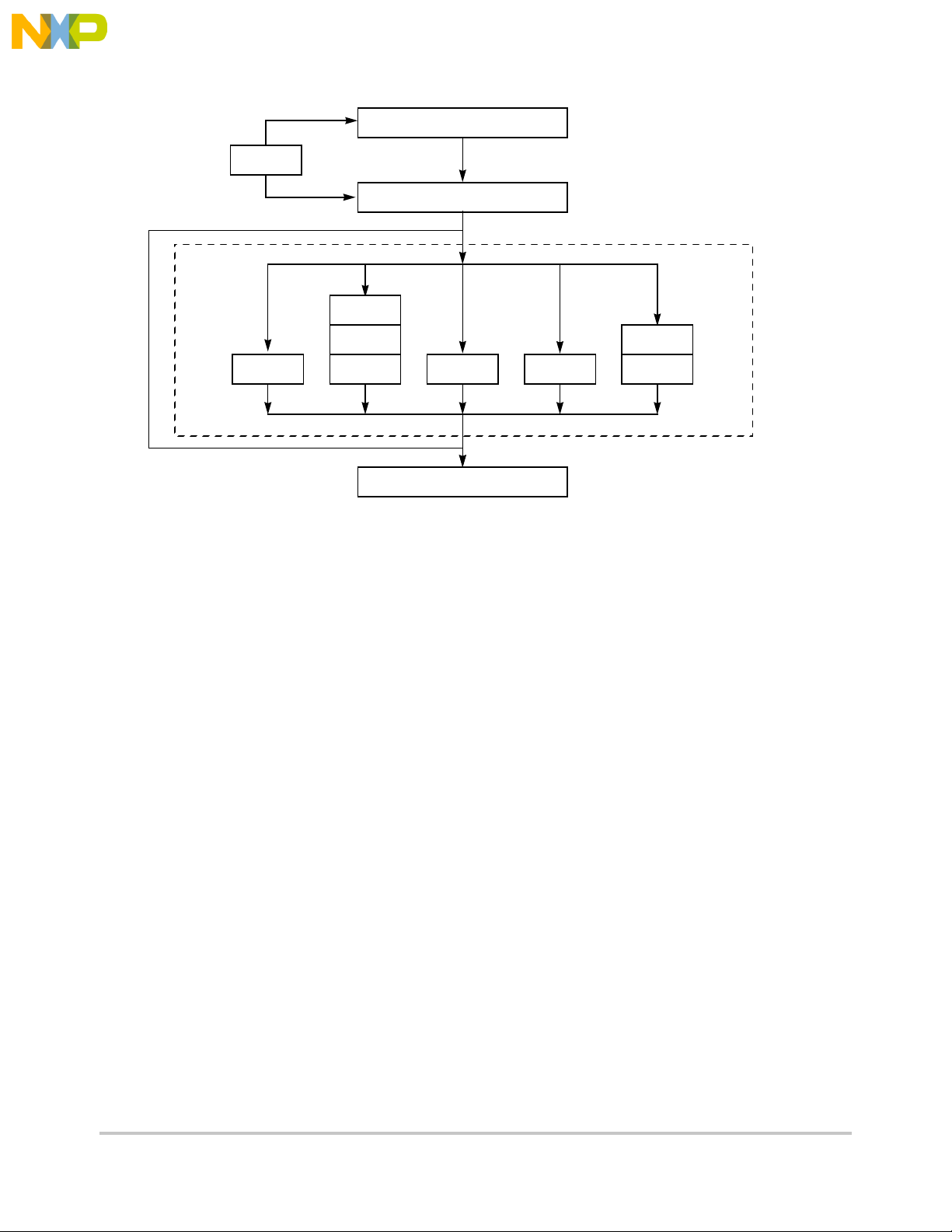
Instruction Timing
Freescale Semiconductor, Inc.
..
.
nc
BPU
Fetch
Dispatch
FPU1
FPU2
FPU3SRU IU2IU1
Complete (Write-Back)
Figure 1-6. Pipeline Diagram
Maximum four-instruction fetch
per clock cycle
Maximum three-instruction dispatch
per clock cycle (includes one branch
instruction)
Execute Stage
LSU1
LSU2
Maximum two-instruction completion per clock cycle
Note that Figure 1-6 does not sho w features, such as reservation stations and rename buf fers
that reduce stalls and improve instruction throughput.
The instruction pipeline in the MPC750 has four major pipeline stages, described as
follows:
• The fetch pipeline stage primarily inv olves retrie ving instructions from the memory
system and determining the location of the next instruction fetch. The BPU decodes
branches during the fetch stage and removes those that do not update CTR or LR
from the instruction stream.
• The dispatch stage is responsible for decoding the instructions supplied by the
instruction fetch stage and determining which instructions can be dispatched in the
current cycle. If source operands for the instruction are av ailable, they are read from
Freescale Semiconductor, I
the appropriate register file or rename register to the execute pipeline stage. If a
source operand is not available, dispatch pro vides a tag that indicates which rename
register will supply the operand when it becomes available. At the end of the
dispatch stage, the dispatched instructions and their operands are latched by the
appropriate execution unit.
• Instructions executed by the IUs, FPU, SRU, and LSU are dispatched from the
bottom two positions in the instruction queue. In a single clock cycle, a maximum
of two instructions can be dispatched to these execution units in any combination.
When an instruction is dispatched, it is assigned a position in the six-entry
completion queue. A branch instruction can be issued on the same clock cycle for a
maximum three-instruction dispatch.
MPC750 RISC Microprocessor Family User’s Manual
For More Information On This Product,
Go to: www.freescale.com
Page 75

..
.
nc
Freescale Semiconductor, I
Freescale Semiconductor, Inc.
Power Management
• During the execute pipeline stage, each execution unit that has an executable
instruction executes the selected instruction (perhaps over multiple cycles), writes
the instruction's result into the appropriate rename register, and notifies the
completion stage that the instruction has finished execution. In the case of an internal
exception, the execution unit reports the e xception to the completion pipeline stage
and (except for the FPU) discontinues instruction execution until the exception is
handled. The exception is not signaled until that instruction is the next to be
completed. Execution of most floating-point instructions is pipelined within the FPU
allowing up to three instructions to be ex ecuting in the FPU concurrently. The FPU
stages are multiply, add, and round-convert. Execution of most load/store
instructions is also pipelined. The load/store unit has two pipeline stages. The first
stage is for effectiv e address calculation and MMU translation and the second stage
is for accessing the data in the cache.
• The complete pipeline stage maintains the correct architectural machine state and
transfers execution results from the rename registers to the GPRs and FPRs (and
CTR and LR, for some instructions) as instructions are retired. As with dispatching
instructions from the instruction queue, instructions are retired from the two bottom
positions in the completion queue. If completion logic detects an instruction causing
an exception, all following instructions are cancelled, their execution results in
rename registers are discarded, and instructions are fetched from the appropriate
exception vector.
Because the PowerPC architecture can be applied to such a wide variety of
implementations, instruction timing varies among processors of this family.
For a detailed discussion of instruction timing with examples and a table of latencies for
each execution unit, see Chapter 6, “Instruction Timing.”
1.10 Power Management
The MPC750 provides four power modes, selectable by setting the appropriate control bits
in the MSR and HID0 registers. The four power modes are as follows:
• Full-power—This is the default power state of the MPC750. The MPC750 is fully
powered and the internal functional units are operating at the full processor clock
speed. If the dynamic power management mode is enabled, functional units that are
idle will automatically enter a low-power state without affecting performance,
software execution, or external hardware.
• Doze—All the functional units of the MPC750 are disabled except for the time
base/decrementer registers and the bus snooping logic. When the processor is in
doze mode, an external asynchronous interrupt, a system management interrupt, a
decrementer exception, a hard or soft reset, or machine check brings the MPC750
into the full-power state. The MPC750 in doze mode maintains the PLL in a fully
For More Information On This Product,
Chapter 1. Overview
Go to: www.freescale.com
Page 76

..
.
nc
Thermal Management
Freescale Semiconductor, Inc.
powered state and locked to the system external clock input (SYSCLK) so a
transition to the full-power state takes only a few processor clock cycles.
• Nap—The nap mode further reduces power consumption by disabling bus snooping,
leaving only the time base register and the PLL in a powered state. The MPC750
returns to the full-power state upon receipt of an external asynchronous interrupt, a
system management interrupt, a decrementer exception, a hard or soft reset, or a
machine check input (MCP
a few processor clock cycles. When the processor is in nap mode, if QA
). A return to full-power state from a nap state takes only
CK is
negated, the processor is put in doze mode to support snooping.
• Sleep—Sleep mode minimizes power consumption by disabling all internal
functional units, after which external system logic may disable the PLL and
SYSCLK. Returning the MPC750 to the full-power state requires the enabling of the
PLL and SYSCLK, followed by the assertion of an external asynchronous interrupt,
a system management interrupt, a hard or soft reset, or a machine check input (MCP
signal after the time required to relock the PLL.
)
Chapter 10, “Power and Thermal Management,” provides information about power saving
and thermal management modes for the MPC750.
1.11 Thermal Management
The MPC750’s thermal assist unit (TAU) provides a way to control heat dissipation. This
ability is particularly useful in portable computers, which, due to power consumption and
size limitations, cannot use desktop cooling solutions such as fans. Therefore, better heat
sink designs coupled with intelligent thermal management is of critical importance for high
performance portable systems.
Primarily, the thermal management system monitors and regulates the system’s operating
temperature. For example, if the temperature is about to exceed a set limit, the system can
be made to slow down or even suspend operations temporarily in order to lower the
temperature.
The thermal management facility also ensures that the processor’s junction temperature
Freescale Semiconductor, I
does not exceed the operating specification. To avoid the inaccuracies that arise from
measuring junction temperature with an external thermal sensor, the MPC750’s on-chip
thermal sensor and logic tightly couples the thermal management implementation.
The TAU consists of a thermal sensor, digital-to-analog convertor, comparator, control
logic, and the dedicated SPRs described in Section 1.4, “PowerPC Registers and
Programming Model.” The TAU does the following:
• Compares the junction temperature against user-programmable thresholds
• Generates a thermal management interrupt if the temperature crosses the threshold
• Enables the user to estimate the junction temperature by way of a software
successive approximation routine
MPC750 RISC Microprocessor Family User’s Manual
For More Information On This Product,
Go to: www.freescale.com
Page 77

..
.
nc
Freescale Semiconductor, Inc.
Performance Monitor
The TAU is controlled through the privileged mtspr/mfspr instructions to the three SPRs
provided for configuring and controlling the sensor control logic, which function as
follows:
• THRM1 and THRM2 provide the ability to compare the junction temperature
against two user-provided thresholds. Having dual thresholds gives the thermal
management software finer control of the junction temperature. In single threshold
mode, the thermal sensor output is compared to only one threshold in either THRM1
or THRM2.
• THRM3 is used to enable the TAU and to control the comparator output sample
time. The thermal management logic manages the thermal management interrupt
generation and time multiplexed comparisons in the dual threshold mode as well as
other control functions.
Instruction cache throttling provides control of the MPC750’ s o v erall junction temperature
by determining the interval at which instructions are fetched. This feature is accessed
through the ICTC register.
Chapter 10, “Power and Thermal Management,” provides information about power saving
and thermal management modes for the MPC750.
1.12 Performance Monitor
The MPC750 incorporates a performance monitor facility that system designers can use to
help bring up, debug, and optimize software performance. The performance monitor counts
events during execution of code, relating to dispatch, execution, completion, and memory
accesses.
The performance monitor incorporates several registers that can be read and written to by
supervisor-level software. User-level versions of these registers provide read-only access
for user-level applications. These registers are described in Section 1.4, “PowerPC
Registers and Programming Model.” Performance monitor control registers, MMCR0 or
MMCR1, can be used to specify which events are to be counted and the conditions for
which a performance monitoring interrupt is taken. Additionally, the sampled instruction
Freescale Semiconductor, I
address register , SIA (USIA), holds the address of the first instruction to complete after the
counter overflowed.
Attempting to write to a user-read-only performance monitor register causes a program
exception, regardless of the MSR[PR] setting.
When a performance monitoring interrupt occurs, program execution continues from
vector offset 0x00F00.
Chapter 11, “Performance Monitor,” describes the operation of the performance monitor
diagnostic tool incorporated in the MPC750.
For More Information On This Product,
Chapter 1. Overview
Go to: www.freescale.com
Page 78

..
.
nc
Performance Monitor
Freescale Semiconductor, Inc.
Freescale Semiconductor, I
MPC750 RISC Microprocessor Family User’s Manual
For More Information On This Product,
Go to: www.freescale.com
Page 79

Freescale Semiconductor, Inc.
Chapter 2
Programming Model
This chapter describes the MPC750 programming model, emphasizing those features
specific to the MPC750 processor and summarizing those that are common to the
..
.
processors that implement the PowerPC architecture. It consists of three major sections,
which describe the following:
nc
Freescale Semiconductor, I
• Registers implemented in the MPC750
• Operand conventions
• The MPC750 instruction set
For detailed information about architecture-defined features, see the Programming
Environments Manual.
Note that the MPC755 microprocessor is a derivative of the MPC750 and all descriptions
for the MPC750 apply for the MPC755 except as noted in Appendix C, “MPC755
Embedded G3 Microprocessor.”
2.1 The MPC750 Processor Register Set
This section describes the registers implemented in the MPC750. It includes an overview
of registers defined by the PowerPC architecture, highlighting differences in how these
registers are implemented in the MPC750, and a detailed description of MPC750-specific
registers. Full descriptions of the architecture-defined register set are provided in Chapter 2,
“PowerPC Register Set,” in the Programming Environments Manual.
Registers are defined at all three levels of the PowerPC architecture—user instruction set
architecture (UISA), virtual environment architecture (VEA), and operating environment
architecture (OEA). The PowerPC architecture defines re gister-to-register operations for all
computational instructions. Source data for these instructions are accessed from the on-chip
registers or are provided as immediate values embedded in the opcode. The three-register
instruction format allows specification of a target register distinct from the two source
registers, thus preserving the original data for use by other instructions and reducing the
number of instructions required for certain operations. Data is transferred between memory
and registers with explicit load and store instructions only.
Chapter 2. Programming Model
For More Information On This Product,
Go to: www.freescale.com
Page 80

..
.
nc
Freescale Semiconductor, Inc.
The MPC750 Processor Register Set
2.1.1 Register Set
The PowerPC UISA registers are user-level. General-purpose registers (GPRs) and
floating-point registers (FPRs) are accessed through instruction operands. Access to
registers can be explicit (by using instructions for that purpose such as Move to
Special-Purpose Register (mtspr) and Move from Special-Purpose Register (mfspr)
instructions) or implicit as part of the execution of an instruction. Some registers are
accessed both explicitly and implicitly.
The registers implemented on the MPC750 are shown in Figure 2-1. The number to the
right of the special-purpose registers (SPRs) indicates the number that is used in the syntax
of the instruction operands to access the register (for example, the number used to access
the integer exception register (XER) is SPR 1). These registers can be accessed using the
mtspr and mfspr instructions.
Freescale Semiconductor, I
MPC750 RISC Microprocessor Family User’s Manual
For More Information On This Product,
Go to: www.freescale.com
Page 81

USER MODEL—VEA
Time Base Facility (For Reading)
TBL
TBR 268
TBU
Freescale Semiconductor, Inc.
The MPC750 Processor Register Set
SUPERVISOR MODEL—OEA
Configuration Registers
Processor
Version
Register
SPR 287PVR
TBR 269
Hardware
Implementation
Registers
HID0
HID1
1
SPR 1008
SPR 1009
Machine State
Register
MSR
..
.
nc
Freescale Semiconductor, I
USER MODEL—UISA
Count
Register
CTR
XER
XER
Link Register
LR
SPR 9
SPR 1
SPR 8
Performance
Monitor Registers
(For Reading)
Performance Counters
UPMC1
UPMC2
UPMC3
UPMC4
Sampled Instruction
Address
USIA
Monitor Control
UMMCR0
UMMCR1
SPR 937
SPR 938
SPR 941
SPR 942
1
SPR 939
1
SPR 936
SPR 940
Performance Monitor Registers
Performance
1
Counters
PMC1
PMC2
PMC3
PMC4
SPR 953
SPR 954
SPR 957
SPR 958
1
General-Purpose
Registers
GPR0
GPR1
GPR31
Floating-Point
Registers
FPR0
FPR1
FPR31
Condition
Register
CR
Floating-Point
Status and
Control Register
FPSCR
Sampled
Instruction
1
Address
SIA SPR 955
Monitor Control
MMCR0
MMCR1
1
SPR 952
SPR 956
Memory Management Registers
Instruction BAT
Registers
IBAT0U
IBAT0L
IBAT1U
IBAT1L
IBAT2U
IBAT2L
IBAT3U
IBAT3L
SPR 528
SPR 529
SPR 530
SPR 531
SPR 532
SPR 533
SPR 534
SPR 535
Exception Handling Registers
SPRGs
SPRG0
SPRG1
SPRG2
SPRG3
SPR 272
SPR 273
SPR 274
SPR 275
Miscellaneous Registers
Register
EAR
Data Address
Breakpoint Register
DABR SPR 1013
SPR 282
Power/Thermal Management Registers
Thermal Assist
Unit Registers
THRM1
THRM2
THRM3
Data BAT
Registers
DBAT0U
DBAT0L
DBAT1U
DBAT1L
DBAT2U
DBAT2L
DBAT3U
DBAT3L
Data Address
Register
DAR
DSISR
DSISR
Time Base
(For Writing)
TBL SPR 284
TBU SPR 285
L2 Control
1, 2
Register
L2CR SPR 1017
1
SPR 1020
SPR 1021
SPR 1022
SPR 536
SPR 537
SPR 538
SPR 539
SPR 540
SPR 541
SPR 542
SPR 543
SPR 19
SPR 18
Instruction Cache
Throttling Control
1
Register
ICTC SPR 1019
Segment
Registers
SR0
SR1
SR15
SDR1
SDR1 SPR 25
Save and Restore
Registers
SRR0 SPR 26
SRR1 SPR 27
DecrementerExternal Access
DEC SPR 22
Instruction Address
Breakpoint Register
IABR SPR 1010
1
1
These registers are MPC750-speci c registers . They may not be supported by other processors that implement the
PowerPC architecture.
2
Not supported by the MPC740.
Figure 2-1. Programming Model—MPC750 Microprocessor Registers
Chapter 2. Programming Model
For More Information On This Product,
Go to: www.freescale.com
Page 82

..
.
nc
Freescale Semiconductor, Inc.
The MPC750 Processor Register Set
Implementation Note—The MPC750 fully decodes the SPR field of the instruction. If the
SPR specified is undefined, the illegal instruction program exception occurs. The user -level
registers are described as follows:
• User-level registers (UISA)—The user-level registers can be accessed by all
software with either user or supervisor privileges. They include the following:
— General-purpose registers (GPRs). The thirty-two GPRs (GPR0–GPR31) serve
as data source or destination registers for integer instructions and provide data
for generating addresses. See “General Purpose Registers (GPRs), ” in Chapter 2,
“PowerPC Register Set,” of the Programming Environments Manual for more
information.
— Floating-point registers (FPRs). The thirty-two FPRs (FPR0–FPR31) serve as
the data source or destination for all floating-point instructions. See
“Floating-Point Registers (FPRs), ” in Chapter 2, “PowerPC Register Set,” of the
Programming Environments Manual.
— Condition register (CR). The 32-bit CR consists of eight 4-bit fields, CR0–CR7,
that reflect results of certain arithmetic operations and provide a mechanism for
testing and branching. See “Condition Register (CR),” in Chapter 2, “PowerPC
Register Set,” of the Programming Environments Manual.
— Floating-point status and control register (FPSCR). The FPSCR contains all
floating-point exception signal bits, exception summary bits, exception enable
bits, and rounding control bits needed for compliance with the IEEE 754
standard. See “Floating-Point Status and Control Register (FPSCR),” in
Chapter 2, “PowerPC Register Set,” of the Programming Environments Manual.
The remaining user-level registers are SPRs. Note that the PowerPC architecture
provides a separate mechanism for accessing SPRs (the mtspr and mfspr
instructions). These instructions are commonly used to explicitly access certain
registers, while other SPRs may be more typically accessed as the side effect of
executing other instructions.
— Integer exception register (XER). The XER indicates overflow and carries for
integer operations. See “XER Register (XER), ” in Chapter 2, “Po werPC Register
Freescale Semiconductor, I
Set,” of the Programming Environments Manual for more information.
Implementation Note—To allow emulation of the lscbx instruction defined by
the POWER architecture, XER[16–23] is implemented so that they can be read
with mfspr[XER] and written with mtxer[XER] instructions.
— Link register (LR). The LR provides the branch target address for the Branch
Conditional to Link Register (bclrx) instruction, and can be used to hold the
logical address of the instruction that follows a branch and link instruction,
typically used for linking to subroutines. See “Link Register (LR), ” in Chapter 2,
“PowerPC Register Set,” of the Programming Environments Manual.
— Count register (CTR). The CTR holds a loop count that can be decremented
during execution of appropriately coded branch instructions. The CTR can also
MPC750 RISC Microprocessor Family User’s Manual
For More Information On This Product,
Go to: www.freescale.com
Page 83

Freescale Semiconductor, Inc.
The MPC750 Processor Register Set
provide the branch target address for the Branch Conditional to Count Register
(bcctrx) instruction. See “Count Register (CTR),” in Chapter 2, “PowerPC
Register Set,” of the Programming Environments Manual.
• User-level registers (VEA)—The PowerPC VEA defines the time base facility
(TB), which consists of two 32-bit registers—time base upper (TBU) and time base
lower (TBL). The time base registers can be written to only by supervisor-level
instructions but can be read by both user- and supervisor-level software. For more
information, see “PowerPC VEA Register Set—Time Base,” in Chapter 2,
“PowerPC Register Set,” of the Programming Environments Manual.
• Supervisor-level registers (OEA)—The OEA defines the registers an operating
system uses for memory management, configuration, exception handling, and other
operating system functions. The OEA defines the following supervisor-level
..
.
registers for 32-bit implementations:
nc
Freescale Semiconductor, I
— Configuration registers
– Machine state register (MSR). The MSR defines the state of the processor.
The MSR can be modified by the Move to Machine State Register (mtmsr),
System Call (sc), and Return from Exception (rfi) instructions. It can be read
by the Move from Machine State Register (mfmsr) instruction. When an
exception is taken, the contents of the MSR are saved to the machine status
save/restore register 1 (SRR1), which is described below . See “Machine State
Register (MSR), ” in Chapter 2, “PowerPC Register Set,” of the Programming
Environments Manual for more information.
Implementation Note—Table 2-1 describes MSR bits the MPC750
implements that are not required by the PowerPC architecture.
Table 2-1. Additional MSR Bits
Bit Name Description
13 POW Power management enable. Optional to the PowerPC architecture.
0 Power management is disabled.
1 Power management is enabled. The processor can enter a power-saving mode when additional
conditions are present. The mode chosen is determined by the DOZE, NAP, and SLEEP bits in
the hardware implementation-dependent register 0 (HID0), described in Table 2-4.
29 PM Performance monitor marked mode. This bit is speci c to the MPC750, and is de ned as reser ved
by the PowerPC architecture. See Chapter 11, “Performance Monitor.”
0 Process is not a marked process.
1 Process is a marked process.
Note that setting MSR[EE] masks not only the architecture-defined external
interrupt and decrementer exceptions but also the MPC750-specific system
management, performance monitor, and thermal management exceptions.
– Processor version register (PVR). This register is a read-only register that
identifies the version (model) and revision level of the processor. For more
Chapter 2. Programming Model
For More Information On This Product,
Go to: www.freescale.com
Page 84

..
.
nc
Freescale Semiconductor, Inc.
The MPC750 Processor Register Set
information, see “Processor Version Register (PVR),” in Chapter 2,
“PowerPC Register Set,” of the Programming Environments Manual.
Implementation Note—The processor version number is 0x0008 for the
MPC750. The processor revision le vel starts at 0x0100 and is updated for each
silicon revision.
— Memory management registers
– Block-address translation (BAT) registers. The PowerPC OEA includes an
array of block address translation registers that can be used to specify four
blocks of instruction space and four blocks of data space. The BAT registers
are implemented in pairs—four pairs of instruction BATs (IB AT0U–IBAT3U
and IBAT0L–IB AT3L) and four pairs of data BATs (DB AT0U–DBAT3U and
DBAT0L–DB AT3L). Figure 2-1 lists the SPR numbers for the BAT registers.
For more information, see “BAT Registers,” in Chapter 2, “Po werPC Register
Set,” of the Programming Environments Manual. Because BAT upper and
lower words are loaded separately , software must ensure that B A T translations
are correct during the time that both BAT entries are being loaded.
The MPC750 implements the G bit in the IBAT registers; ho wever , attempting
to execute code from an IBAT area with G = 1 causes an ISI exception. This
complies with the revision of the architecture described in the Programming
Environments Manual
– SDR1. The SDR1 register specifies the page table base address used in
virtual-to-physical address translation. See “SDR1, ” in Chapter 2, “PowerPC
Register Set,” of the Programming Environments Manual.”
– Segment registers (SR). The PowerPC OEA defines sixteen 32-bit segment
registers (SR0–SR15). Note that the SRs are implemented on 32-bit
implementations only. The fields in the segment register are interpreted
differently depending on the value of bit 0. See “Segment Registers,” in
Chapter 2, “PowerPC Register Set,” of the Programming Environments
Manual for more information.
Note that the MPC750 implements separate memory management units
Freescale Semiconductor, I
(MMUs) for instruction and data. It associates the architecture-defined SRs
.
with the data MMU (DMMU). It reflects the values of the SRs in separate,
so-called ‘shadow’ segment registers in the instruction MMU (IMMU).
— Exception-handling registers
– Data address register (D AR). After a DSI or an alignment e xception, DAR is
set to the effective address (EA) generated by the faulting instruction. See
“Data Address Register (DAR),” in Chapter 2, “Po werPC Register Set, ” of the
Programming Environments Manual for more information.
– SPRG0–SPRG3. The SPRG0–SPRG3 registers are provided for operating
system use. See “SPRG0–SPRG3, ” in Chapter 2, “PowerPC Register Set,” of
the Programming Environments Manual for more information.
MPC750 RISC Microprocessor Family User’s Manual
For More Information On This Product,
Go to: www.freescale.com
Page 85
Freescale Semiconductor, Inc.
The MPC750 Processor Register Set
– DSISR. The DSISR register defines the cause of DSI and alignment
exceptions. See “DSISR,” in Chapter 2, “PowerPC Register Set,” of the
Programming Environments Manual for more information.
– Machine status save/restore register 0 (SRR0). The SRR0 register is used to
save the address of the instruction at which execution continues when rfi
executes at the end of an exception handler routine.
See “Machine Status
Save/Restore Register 0 (SRR0),” in Chapter 2, “PowerPC Register Set,” of
the Programming Environments Manual for more information.
– Machine status save/restore register 1 (SRR1). The SRR1 register is used to
save machine status on exceptions and to restore machine status when rfi
executes.
See “Machine Status Save/Restore Register 1 (SRR1),” in
Chapter 2, “PowerPC Register Set,” of the Programming Environments
..
.
Manual for more information.
nc
Freescale Semiconductor, I
Implementation Note—When a machine check exception occurs, the
MPC750 sets one or more error bits in SRR1. Table 2-2 describes SRR1 bits
the MPC750 implements that are not required by the PowerPC architecture.
Table 2-2. Additional SRR1 Bits
Bit Name Description
11 L2DP Set by a data parity error on the L2 bus. The MPC740 does not implement the L2 cache interface.
12 MCPIN Set by the assertion of MCP
13 TEA Set by a TEA assertion on the 60x bus
14 DP Set by a data parity error on the 60x bus
15 AP Set by an address parity error on the 60x bus
— Miscellaneous registers
– Time base (TB). The TB is a 64-bit structure provided for maintaining the
time of day and operating interval timers. The TB consists of two 32-bit
registers—time base upper (TBU) and time base lower (TBL). The time base
registers can be written to only by supervisor-level software, but can be read
by both user- and supervisor-level software. See “Time Base Facility
(TB)—OEA,” in Chapter 2, “PowerPC Register Set,” of the Programming
Environments Manual for more information.
– Decrementer register (DEC). This register is a 32-bit decrementing counter
that provides a mechanism for causing a decrementer exception after a
programmable delay; the frequency is a subdivision of the processor clock.
See “Decrementer Register (DEC), ” in Chapter 2, “PowerPC Register Set, ” of
the Programming Environments Manual for more information.
Implementation Note—In the MPC750 the decrementer register is
decremented and the time base is incremented at a speed that is one-fourth the
speed of the bus clock.
Chapter 2. Programming Model
For More Information On This Product,
Go to: www.freescale.com
Page 86

Freescale Semiconductor, Inc.
The MPC750 Processor Register Set
– Data address breakpoint register (DABR)—This optional register is used to
cause a breakpoint exception if a specified data address is encountered. See
“Data Address Breakpoint Register (DABR),” in Chapter 2, “PowerPC
Register Set,” of the Programming Environments Manual.
– External access register (EAR). This optional register is used in conjunction
with eciwx and ecowx. Note that the EAR register and the eciwx and ecowx
instructions are optional in the PowerPC architecture and may not be
supported in all processors that implement the OEA. See “External Access
Register (EAR),” in Chapter 2, “PowerPC Re gister Set,” of the Programming
Environments Manual for more information.
• MPC750-specific registers—The PowerPC architecture allows implementationspecific SPRs. Those incorporated in the MPC750 are described as follows. Note
..
.
that in the MPC750, these registers are all supervisor-level registers.
nc
Freescale Semiconductor, I
— Instruction address breakpoint register (IABR)—This register can be used to
cause a breakpoint exception if a specified instruction address is encountered.
— Hardware implementation-dependent register 0 (HID0)—This register controls
various functions, such as enabling checkstop conditions, and locking, enabling,
and invalidating the instruction and data caches.
— Hardware implementation-dependent register 1 (HID1)—This register reflects
the state of PLL_CFG[0–3] clock signals.
— The L2 cache control register (L2CR) is used to configure and operate the L2
cache. It includes bits for enabling parity checking, setting the L2-to-processor
clock ratio, and identifying the type of RAM used for the L2 cache
implementation. (Not supported in the MPC740.)
— Performance monitor registers. The following registers are used to define and
count events for use by the performance monitor:
– The performance monitor counter registers (PMC1–PMC4) are used to record
the number of times a certain event has occurred. UPMC1–UPMC4 provide
user-level read access to these registers.
– The monitor mode control registers (MMCR0–MMCR1) are used to enable
various performance monitor interrupt functions. UMMCR0–UMMCR1
provide user-level read access to these registers.
– The sampled instruction address register (SIA) contains the effecti v e address
of an instruction executing at or around the time that the processor signals the
performance monitor interrupt condition. USIA provides user-level read
access to the SIA.
– The MPC750 does not implement the sampled data address register (SD A) or
the user-level, read-only USDA registers. However, for compatibility with
processors that do, those registers can be written to by boot code without
causing an exception. SDA is SPR 959; USDA is SPR 943.
MPC750 RISC Microprocessor Family User’s Manual
For More Information On This Product,
Go to: www.freescale.com
Page 87

..
.
nc
Freescale Semiconductor, Inc.
The MPC750 Processor Register Set
— The instruction cache throttling control register (ICTC) has bits for enabling the
instruction cache throttling feature and for controlling the interval at which
instructions are forwarded to the instruction buffer in the fetch unit. This
provides control over the processor’s overall junction temperature.
— Thermal management registers (THRM1, THRM2, and THRM3). Used to
enable and set thresholds for the thermal management facility.
– THRM1 and THRM2 provide the ability to compare the junction temperature
against two user-provided thresholds. The dual thresholds allow the thermal
management software differing degrees of action in lowering the junction
temperature. The TAU can be also operated in a single threshold mode in
which the thermal sensor output is compared to only one threshold in either
THRM1 or THRM2.
– THRM3 is used to enable the thermal management assist unit (TAU) and to
control the comparator output sample time.
Note that while it is not guaranteed that the implementation of MPC750-specific registers
is consistent among processors of this family, other processors may implement similar or
identical registers.
2.1.2 MPC750-Specific Registers
This section describes registers that are defined for the MPC750 but are not included in the
PowerPC architecture.
2.1.2.1 Instruction Address Breakpoint Register (IABR)
The address breakpoint register (IABR), shown in Figure 2-2, supports the instruction
address breakpoint exception. When this exception is enabled, instruction fetch addresses
are compared with an effective address stored in the IABR. If the word specified in the
IABR is fetched, the instruction breakpoint handler is inv oked. The instruction that triggers
the breakpoint does not execute before the handler is invoked. For more information, see
Section 4.5.14, “Instruction Address Breakpoint Exception (0x01300).” The IABR can be
Freescale Semiconductor, I
accessed with mtspr and mfspr using the SPR1010.
Address
0 29 30 31
Figure 2-2. Instruction Address Breakpoint Register
The IABR bits are described in Table 2-3.
BE TE
Chapter 2. Programming Model
For More Information On This Product,
Go to: www.freescale.com
Page 88

Freescale Semiconductor, Inc.
The MPC750 Processor Register Set
Table 2-3. Instruction Address Breakpoint Register Bit Settings
Bits Name Description
0–29 Address Word address to be compared
30 BE Breakpoint enabled. Setting this bit indicates that breakpoint checking is to be done.
31 TE Translation enabled. An IABR match is signaled if this bit matches MSR[IR].
2.1.2.2 Hardware Implementation-Dependent Register 0
The hardware implementation-dependent register 0 (HID0) controls the state of several
functions within the MPC750. The HID0 register is shown in Figure 2-3.
..
.
nc
Freescale Semiconductor, I
DLOCK
EMCP BCLK ECLK DOZE SLEEP ILOCK
DBP
EBDEBA PAR NAP DPM NHR ICE DCE DCFI
0 1 2 3 4 5 6 7 8 9 10111213141516171819202122232425262728293031
0
0
0
0
ICFI SPD
IFEM SGE
DCFA BTIC
0
BHTABE
Reserved
NOOPTI
0
Figure 2-3. Hardware Implementation-Dependent Register 0 (HID0)
The HID0 bits are described in Table 2-4.
Table 2-4. HID0 Bit Functions
Bits Name Function
0 EMCP Enable MCP
by assertion of MCP
0 Masks MCP
1 Asserting MCP
1 DBP Disable 60x bus address and data parity generation.
0 The system generates address and data parity.
1 Parity generation is disabled and parity signals are driven to 0 during bus operations. When parity
generation is disabled, all parity checking should also be disabled and parity signals need not be
connected.
2 EBA Enable/disable 60x bus address parity checking
0 Prevents address parity checking.
1 Allows a address parity error to cause a checkstop if MSR[ME] = 0 or a machine check exception
if MSR[ME] = 1.
EBA and EBD allow the processor to operate with memory subsystems that do not generate parity.
. The primary purpose of this bit is to mask out further machine check exceptions caused
, similar to how MSR[EE] can mask external interrupts.
. Asserting MCP does not generate a machine check exception or a checkstop.
causes checkstop if MSR[ME] = 0 or a machine check exception if ME = 1.
3 EBD Enable 60x bus data parity checking
0 Parity checking is disabled.
1 Allows a data parity error to cause a checkstop if MSR[ME] = 0 or a machine check exception if
MSR[ME] = 1.
EBA and EBD allow the processor to operate with memory subsystems that do not generate parity.
4 BCLK CLK_OUT output enable and clock type selection. Used in conjunction with HID0[ECLK] and the
HRESET
5 — Not used. De ned as EICE on some ear lier processors.
signal to con gure CLK_OUT. See Table 2-5.
MPC750 RISC Microprocessor Family User’s Manual
For More Information On This Product,
Go to: www.freescale.com
Page 89

Freescale Semiconductor, Inc.
The MPC750 Processor Register Set
Table 2-4. HID0 Bit Functions (continued)
Bits Name Function
6 ECLK CLK_OUT output enable and clock type selection. Used in conjunction with HID0[BCLK] and the
HRESET
7 PAR Disable precharge of ARTRY.
0 Precharge of AR
1 Alters bus protocol slightly by preventing the processor from driving AR
8 DOZE Doze mode enable. Operates in conjunction with MSR[POW].
0 Doze mode disabled.
1 Doze mode enabled. Doze mode is invoked by setting MSR[POW] while this bit is set. In doze
signal to con gure CLK_OUT. See Table 2-5.
TRY enabled
TRY to high (negated)
state. If this is done, the system must restore the signals to the high state.
mode, the PLL, time base, and snooping remain active.
..
.
nc
Freescale Semiconductor, I
9 NAP Nap mode enable. Operates in conjunction with MSR[POW].
0 Nap mode disabled.
1 Nap mode enabled. Doze mode is invoked by setting MSR[POW] while this bit is set. In nap mode,
the PLL and the time base remain active.
10 SLEEP Sleep mode enable. Operates in conjunction with MSR[POW].
0 Sleep mode disabled.
1 Sleep mode enabled. Sleep mode is invoked by setting MSR[POW] while this bit is set. QREQ
asserted to indicate that the processor is ready to enter sleep mode. If the system logic
determines that the processor may enter sleep mode, the quiesce acknowledge signal, QA
asserted back to the processor. Once QA
mode after several processor clocks. At this point, the system logic may turn off the PLL by rst
con gur ing PLL_CFG[0–3] to PLL bypass mode, then disabling SYSCLK.
11 DPM Dynamic power management enable.
0 Dynamic power management is disabled.
1 Functional units enter a low-power mode automatically if the unit is idle. This does not affect
operational performance and is transparent to software or any external hardware.
12–14 — Not used
15 NHR Not hard reset (software-use only)—Helps software distinguish a hard reset from a soft reset.
0 A hard reset occurred if software had previously set this bit.
1 A hard reset has not occurred. If software sets this bit after a hard reset, when a reset occurs and
this bit remains set, software can tell it was a soft reset.
16 ICE Instruction cache enable
0 The instruction cache is neither accessed nor updated. All pages are accessed as if they were
marked cache-inhibited (WIM = xlx). Potential cache accesses from the bus (snoop and cache
operations) are ignored. In the disabled state for the L1 caches, the cache tag state bits are
ignored and all accesses are propagated to the L2 cache or bus as single-beat transactions. For
those transactions, however, CI
regardless of cache disabled status. ICE is zero at power-up.
1 The instruction cache is enabled
re ects the or iginal state determined by address translation
CK assertion is detected, the processor enters sleep
is
CK, is
17 DCE Data cache enable
0 The data cache is neither accessed nor updated. All pages are accessed as if they were marked
cache-inhibited (WIM = xlx). Potential cache accesses from the bus (snoop and cache operations)
are ignored. In the disabled state for the L1 caches, the cache tag state bits are ignored and all
accesses are propagated to the L2 cache or bus as single-beat transactions. For those
transactions, however, CI
of cache disabled status. DCE is zero at power-up.
1 The data cache is enabled.
For More Information On This Product,
re ects the or iginal state determined by address translation regardless
Chapter 2. Programming Model
Go to: www.freescale.com
Page 90

..
.
nc
Freescale Semiconductor, I
Freescale Semiconductor, Inc.
The MPC750 Processor Register Set
Table 2-4. HID0 Bit Functions (continued)
Bits Name Function
18 ILOCK Instruction cache lock
0 Normal operation
1 Instruction cache is locked. A locked cache supplies data normally on a hit, but are treated as a
cache-inhibited transaction on a miss. On a miss, the transaction to the bus or the L2 cache is
single-beat, however, CI
independent of cache locked or disabled status.
To prevent locking during a cache access, an isync instruction must precede the setting of ILOCK.
19 DLOCK Data cache lock.
0 Normal operation
1 Data cache is locked. A locked cache supplies data normally on a hit but is treated as a
cache-inhibited transaction on a miss. On a miss, the transaction to the bus or the L2 cache is
single-beat, however, CI
independent of cache locked or disabled status. A snoop hit to a locked L1 data cache performs
as if the cache were not locked. A cache block invalidated by a snoop remains invalid until the
cache is unlocked.
To prevent locking during a cache access, a sync instruction must precede the setting of DLOCK.
20 ICFI Instruction cache ash in validate
0 The instruction cache is not invalidated. The bit is cleared when the invalidation operation begins
(usually the next cycle after the write operation to the register). The instruction cache must be
enabled for the invalidation to occur.
1 An invalidate operation is issued that marks the state of each instruction cache block as invalid
without writing back modi ed cache b locks to memory. Cache access is blocked during this time.
Bus accesses to the cache are signaled as a miss during invalidate-all operations. Setting ICFI
clears all the valid bits of the blocks and the PLRU bits to point to way L0 of each set. Once the
L1 ash in validate bits are set through a mtspr operations, hardware automatically resets these
bits in the next cycle (provided that the corresponding cache enable bits are set in HID0).
Note that in the MPC603e processors, the proper use of the ICFI and DCFI bits was to set them and
clear them in two consecutive mtspr operations. Software that already has this sequence of
operations does not need to be changed to run on the MPC750.
21 DCFI Data cache ash in validate
0 The data cache is not invalidated. The bit is cleared when the invalidation operation begins
(usually the next cycle after the write operation to the register). The data cache must be enabled
for the invalidation to occur.
1 An invalidate operation is issued that marks the state of each data cache block as invalid without
writing back modi ed cache b locks to memory. Cache access is blocked during this time. Bus
accesses to the cache are signaled as a miss during invalidate-all operations. Setting DCFI clears
all the valid bits of the blocks and the PLRU bits to point to way L0 of each set. Once the L1 ash
invalidate bits are set through a mtspr operations, hardware automatically resets these bits in the
next cycle (provided that the corresponding cache enable bits are set in HID0).
Setting this bit clears all the valid bits of the blocks and the PLRU bits to point to way L0 of each set.
Note that in the MPC603e processors, the proper use of the ICFI and DCFI bits was to set them and
clear them in two consecutive mtspr operations. Software that already has this sequence of
operations does not need to be changed to run on the MPC750.
still re ects the or iginal state as determined by address translation
still re ects the or iginal state as determined by address translation
22 SPD Speculative cache access disable
0 Speculative bus accesses to nonguarded space (G = 0) from both the instruction and data caches
is enabled
1 Speculative bus accesses to nonguarded space in both caches is disabled
23 IFEM Enable M bit on bus for instruction fetches.
0 M bit not re ected on b us for instruction fetches. Instruction fetches are treated as nonglobal on
the bus
1 Instruction fetches re ect the M bit from the WIM settings.
MPC750 RISC Microprocessor Family User’s Manual
For More Information On This Product,
Go to: www.freescale.com
Page 91

..
.
nc
Freescale Semiconductor, Inc.
The MPC750 Processor Register Set
Table 2-4. HID0 Bit Functions (continued)
Bits Name Function
24 SGE Store gathering enable
0 Store gathering is disabled
1 Integer store gathering is performed for write-through to nonguarded space or for cache-inhibited
stores to nonguarded space for 4-byte, word-aligned stores. The LSU combines stores to form a
double word that is sent out on the 60x bus as a single-beat operation. Stores are gathered only
if successive, eligible stores, are queued and pending. Store gathering is performed regardless
of address order or endian mode.
25 DCFA Data cache ush assist. (Force data cache to ignore invalid sets on miss replacement selection.)
0 The data cache ush assist f acility is disabled
1 The miss replacement algorithm ignores invalid entries and follows the replacement sequence
de ned b y the PLRU bits. This reduces the series of uniquely addressed load or dcbz instructions
to eight per set. The bit should be set just before beginning a cache ush routine and should be
cleared when the series of instructions is complete.
26 BTIC BTIC enable. Used to enable use of the 64-entry branch instruction cache.
0 The BTIC contents are invalidated and the BTIC behaves as if it were empty. New entries cannot
be added until the BTIC is enabled.
1 The BTIC is enabled and new entries can be added.
27 — Not used. De ned as FBIOB on ear lier 603-type processors.
28 ABE Address broadcast enable—controls whether certain address-only operations (such as cache
operations, eieio, and sync) are broadcast on the 60x bus.
0 Address-only operations affect only local L1 and L2 caches and are not broadcast.
1 Address-only operations are broadcast on the 60x bus.Affected instructions are eieio, sync,
dcbi, dcbf, and dcbst. A sync instruction completes only after a successful broadcast. Execution
of eieio causes a broadcast that may be used to prevent any external devices, such as a bus
bridge chip, from store gathering.
Note that dcbz (with M = 1, coherency required) always broadcasts on the 60x bus regardless of the
setting of this bit. An icbi is never broadcast. No cache operations, except dcbz, are snooped by the
MPC750 regardless of whether ABE is set. Bus activity caused by these instructions results directly
from performing the operation on the MPC750 cache.
29 BHT Branch history table enable
0 BHT disabled. The MPC750 uses static branch prediction as de ned b y the PowerPC architecture
(UISA) for those branch instructions the BHT would have otherwise used to predict (that is, those
that use the CR as the only mechanism to determine direction). For more information on static
branch prediction, see “Conditional Branch Control,” in Chapter 4 of The Programming
Environments Manual.
1 Allows the use of the 512-entry branch history table (BHT).
The BHT is disabled at power-on reset. All entries are set to weakly, not-taken.
Freescale Semiconductor, I
30 — Not used
31 NOOPTI No-op the data cache touch instructions.
0 The dcbt and dcbtst instructions are enabled.
1 The dcbt and dcbtst instructions are no-oped globally.
Table 2-5 shows how HID0[BCLK], HID0[ECLK], and HRESET are used to configure
CLK_OUT. See Section 7.2.11.2, “Clock Out (CLK_OUT)—Output,” for more
information.
Chapter 2. Programming Model
For More Information On This Product,
Go to: www.freescale.com
Page 92

Freescale Semiconductor, Inc.
The MPC750 Processor Register Set
..
.
nc
Table 2-5. HID0[BCLK] and HID0[ECLK] CLK_OUT Configuration
HRESET HID0[ECLK] HID0[BCLK] CLK_OUT
Asserted x x Bus
Negated 0 0 High impedance
Negated 0 1 Bus/ 2
Negated 1 0 Core
Negated 1 1 Bus
HID0 can be accessed with mtspr and mfspr using SPR1008.
2.1.2.3 Hardware Implementation-Dependent Register 1
The hardware implementation-dependent register 1 (HID1) reflects the state of the
PLL_CFG[0–3] signals. The HID1 bits are shown in Figure 2-4.
Reserved
0
0
0
0
0
0
0
0
0
0
PC1
PC3
PC2PC0
0
234 31
1
0
0
0
0
0
0
0
0
0
0
0
0
0
0
0
0
0
0
Figure 2-4. Hardware Implementation-Dependent Register 1 (HID1)
The HID1 bits are described in Table 2-6.
Table 2-6. HID1 Bit Functions
Bit(s) Name Description
0 PC0 PLL con gur ation bit 0 (read-only)
1 PC1 PLL con gur ation bit 1 (read-only)
2 PC2 PLL con gur ation bit 2 (read-only)
3 PC3 PLL con gur ation bit 3 (read-only)
4–31 — Reserved
Freescale Semiconductor, I
Note: The clock con gur ation bits re ect the state of the PLL_CFG[0–3] signals .
HID1 can be accessed with mtspr and mfspr using SPR 1009.
2.1.2.4 Performance Monitor Registers
This section describes the registers used by the performance monitor , which is described in
Chapter 11, “Performance Monitor.”
MPC750 RISC Microprocessor Family User’s Manual
For More Information On This Product,
Go to: www.freescale.com
Page 93

..
.
nc
Freescale Semiconductor, Inc.
The MPC750 Processor Register Set
2.1.2.4.1 Monitor Mode Control Register 0 (MMCR0)
The monitor mode control register 0 (MMCR0), shown in Figure 2-5, is a 32-bit SPR
provided to specify ev ents to be counted and recorded. The MMCR0 can be accessed only
in supervisor mode. User-level software can read the contents of MMCR0 by issuing an
mfspr instruction to UMMCR0, described in Section 2.1.2.4.2, “User Monitor Mode
Control Register 0 (UMMCR0).”
INTONBITTRANS
RTCSELECT
DISCOUNT
DPDIS
DMSDU PMC1SELECT PMC2SELECT
DMR THRESHOLD
0 1 2 3 4 5 6 7 8 9 10 15 16 17 18 19 25 26 31
PMC2INTCONTROL
PMC1INTCONTROLENINT
PMCTRIGGER
Figure 2-5. Monitor Mode Control Register 0 (MMCR0)
This register must be cleared at power up. Reading this register does not change its
contents. The bits of the MMCR0 register are described in Table 2-7.
Table 2-7. MMCR0 Bit Settings
Bits Name Description
0 DIS Disables counting unconditionally
0 The values of the PMCn counters can be changed by hardware.
1 The values of the PMCn counters cannot be changed by hardware.
1 DP Disables counting while in supervisor mode
0 The PMCn counters can be changed by hardware.
1 If the processor is in supervisor mode (MSR[PR] is cleared), the counters are not
changed by hardware.
2 DU Disables counting while in user mode
0 The PMCn counters can be changed by hardware.
1 If the processor is in user mode (MSR[PR] is set), the PMCn counters are not
changed by hardware.
3 DMS Disables counting while MSR[PM] is set
0 The PMCn counters can be changed by hardware.
1 If MSR[PM] is set, the PMCn counters are not changed by hardware.
Freescale Semiconductor, I
4 DMR Disables counting while MSR(PM) is zero.
0 The PMCn counters can be changed by hardware.
1 If MSR[PM] is cleared, the PMCn counters are not changed by hardware.
5 ENINT Enables performance monitor interrupt signaling.
0 Interrupt signaling is disabled.
1 Interrupt signaling is enabled.
Cleared by hardware when a performance monitor interrupt is signaled. To reenable
these interrupt signals, software must set this bit after handling the performance monitor
interrupt. The IPL ROM code clears this bit before passing control to the operating
system.
Chapter 2. Programming Model
For More Information On This Product,
Go to: www.freescale.com
Page 94

Freescale Semiconductor, Inc.
The MPC750 Processor Register Set
Table 2-7. MMCR0 Bit Settings (continued)
Bits Name Description
6 DISCOUNT Disables counting of PMCn when a performance monitor interrupt is signaled (that is,
((PMCnINTCONTROL = 1) & (PMCn[0] = 1) & (ENINT = 1)) or the occurrence of an
enabled time base transition with ((INTONBITTRANS =1) & (ENINT = 1)).
0 Signaling a performance monitor interrupt does not affect counting status of PMCn.
1 The signaling of a performance monitor interrupt prevents changing of PMC1
counter. The PMCn counter do not change if PMC2COUNTCTL = 0.
Because a time base signal could have occurred along with an enabled counter
over o w condition, software should always reset INTONBITTRANS to zero, if the value
in INTONBITTRANS was a one.
7–8 RTCSELECT 64-bit time base, bit selection enable
00 Pick bit 63 to count
01 Pick bit 55 to count
..
.
10 Pick bit 51 to count
11 Pick bit 47 to count
nc
Freescale Semiconductor, I
9 INTONBITTRANS Cause interrupt signaling on bit transition (identi ed in R TCSELECT) from off to on
0 Do not allow interrupt signal if chosen bit transitions.
1 Signal interrupt if chosen bit transitions.
Software is responsible for setting and clearing INTONBITTRANS.
10–15 THRESHOLD Threshold value. The MPC750 supports all 6 bits, allowing threshold values from 0–63.
The intent of the THRESHOLD support is to characterize L1 data cache misses.
16 PMC1INTCONTROL Enables interrupt signaling due to PMC1 counter over o w.
0 Disable PMC1 interrupt signaling due to PMC1 counter over o w
1 Enable PMC1 Interrupt signaling due to PMC1 counter over o w
17 PMCINTCONTROL Enable interrupt signaling due to any PMC2–PMC4 counter over o w. Overrides the
setting of DISCOUNT.
0 Disable PMC2–PMC4 interrupt signaling due to PMC2–PMC4 counter over o w.
1 Enable PMC2–PMC4 interrupt signaling due to PMC2–PMC4 counter over o w.
18 PMCTRIGGER Can be used to trigger counting of PMC2–PMC4 after PMC1 has over o wed or after a
performance monitor interrupt is signaled.
0 Enable PMC2–PMC4 counting.
1 Disable PMC2–PMC4 counting until either PMC1[0] = 1 or a performance monitor
interrupt is signaled.
19–25 PMC1SELECT PMC1 input selector, 128 events selectable. See Table 2-10.
26–31 PMC2SELECT PMC2 input selector, 64 events selectable. See Table 2-11.
MMCR0 can be accessed with mtspr and mfspr using SPR 952.
2.1.2.4.2 User Monitor Mode Control Register 0 (UMMCR0)
The contents of MMCR0 are reflected to UMMCR0, which can be read by user-level
software. MMCR0 can be accessed with mfspr using SPR 936.
MPC750 RISC Microprocessor Family User’s Manual
For More Information On This Product,
Go to: www.freescale.com
Page 95

Freescale Semiconductor, Inc.
The MPC750 Processor Register Set
2.1.2.4.3 Monitor Mode Control Register 1 (MMCR1)
The monitor mode control register 1 (MMCR1) functions as an event selector for
performance monitor counter registers 3 and 4 (PMC3 and PMC4). The MMCR1 register
is shown in Figure 2-6.
Reserved
..
.
nc
Freescale Semiconductor, I
0
0
0
0
0
0
0
0
PMC3SELECT
045 10 31
PMC4SELECT
9
0
0
0
0
0
0
0
0
0
0
0
0
0
0
Figure 2-6. Monitor Mode Control Register 1 (MMCR1)
Bit settings for MMCR1 are shown in Table 2-8. The corresponding events are described
in Section 2.1.2.4.5, “Performance Monitor Counter Registers (PMC1–PMC4).”
Table 2-8. MMCR1 Bit Settings
Bits Name Description
0–4 PMC3SELECT PMC3 input selector. 32 events selectable. See Table 2-12 for de ned selections .
5–9 PMC4SELECT PMC4 input selector. 32 events selectable. See Table 2-13 for de ned selections .
10–31 — Reserved
MMCR1 can be accessed with mtspr and mfspr using SPR 956. User-level software can
read the contents of MMCR1 by issuing an mfspr instruction to UMMCR1, described in
Section 2.1.2.4.4, “User Monitor Mode Control Register 1 (UMMCR1).”
2.1.2.4.4 User Monitor Mode Control Register 1 (UMMCR1)
The contents of MMCR1 are reflected to UMMCR1, which can be read by user-level
software. MMCR1 can be accessed with mfspr using SPR 940.
2.1.2.4.5 Performance Monitor Counter Registers (PMC1–PMC4)
PMC1–PMC4, shown in Figure 2-7, are 32-bit counters that can be programmed to
generate interrupt signals when they overflow.
OV
01 31
Counter Value
Figure 2-7. Performance Monitor Counter Registers (PMC1–PMC4)
The bits contained in the PMCn registers are described in Table 2-9.
Chapter 2. Programming Model
For More Information On This Product,
Go to: www.freescale.com
Page 96

..
.
nc
Freescale Semiconductor, Inc.
The MPC750 Processor Register Set
Table 2-9. PMCn Bit Settings
Bits Name Description
0 OV Over o w. When this bit is set it indicates that this counter has reached its maximum value.
1–31 Counter value Indicates the number of occurrences of the speci ed e vent.
Counters are considered to overflo w when the high-order bit (the sign bit) becomes set; that
is, they reach the value 2147483648 (0x8000_0000). However, an interrupt is not signaled
unless both PMCn[INTCONTROL] and MMCR0[ENINT] are also set.
Note that the interrupts can be masked by clearing MSR[EE]; the interrupt signal condition
may occur with MSR[EE] cleared, but the exception is not taken until EE is set. Setting
MMCR0[DISCOUNT] forces counters to stop counting when a counter interrupt occurs.
Software is expected to use mtspr to set PMC explicitly to nono verflo w v alues. If software
sets an overflow value, an erroneous exception may occur. For example, if both
PMCn[INTCONTROL] and MMCR0[ENINT] are set and mtspr loads an o v erflow value,
an interrupt signal may be generated without any event counting having taken place.
The event to be monitored can be chosen by setting MMCR0[0–9]. The selected e v ents are
counted beginning when MMCR0 is set until either MMCR0 is reset or a performance
monitor interrupt is generated. Table 2-10 lists the selectable events and their encodings.
Table 2-10. PMC1 Events—MMCR0[19–25] Select Encodings
Encoding Description
000 0000 Register holds current value.
000 0001 Number of processor cycles
000 0010 Number of completed instructions. Does not include folded branches.
0000011 Number of transitions from 0 to 1 of speci ed bits in time base lo wer register. Bits are speci ed through
RTCSELECT (MMRC0[7–8]). 00 = 15, 01 = 19, 10 = 23, 11 = 31
0000100 Number of instructions dispatched—0, 1, or 2 instructions per cycle
0000101 Number of eieio instructions completed
Freescale Semiconductor, I
0000110 Number of cycles spent performing table search operations for the ITLB
0000111 Number of accesses that hit the L2
0001000 Number of valid instruction EAs delivered to the memory subsystem
0001001 Number of times the address of an instruction being completed matches the address in the IABR
0001010 Number of loads that miss the L1 with latencies that exceeded the threshold value
0001011 Number of branches that are unresolved when processed
0001100 Number of cycles the dispatcher stalls due to a second unresolved branch in the instruction stream
All others Reserved. May be used in a later revision.
Bits MMCR0[26–31] specify events associated with PMC2, as shown in Table 2-11.
MPC750 RISC Microprocessor Family User’s Manual
For More Information On This Product,
Go to: www.freescale.com
Page 97

Freescale Semiconductor, Inc.
The MPC750 Processor Register Set
Table 2-11. PMC2 Events—MMCR0[26–31] Select Encodings
Encoding Description
00 0000 Register holds current value.
00 0001 Counts processor cycles.
00 0010 Counts completed instructions. Does not include folded branches.
00 0011 Counts transitions from 0 to 1 of TBL bits speci ed through MMRC0[R TCSELECT]. 00 = 47, 01 = 51, 10
= 55, 11 = 63.
00 0100 Counts instructions dispatched. 0, 1, or 2 instructions per cycle.
00 0101 Counts L1 instruction cache misses.
00 0110 Counts ITLB misses.
..
.
nc
Freescale Semiconductor, I
00 0111 Counts L2 instruction misses.
00 1000 Counts branches predicted or resolved not taken.
00 1001 Counts MSR[PR] bit toggles.
00 1010 Counts times reserved load operations completed.
00 1011 Counts completed load and store instructions.
00 1100 Counts snoops to the L1 and the L2.
00 1101 Counts L1 cast-outs to the L2.
00 1110 Counts completed system unit instructions.
00 1111 Counts instruction fetch misses in the L1.
01 0000 Counts branches allowing out-of-order execution that resolved correctly.
All others Reserved.
Bits MMCR1[0–4] specify events associated with PMC3, as shown in Table 2-12.
Table 2-12. PMC3 Events—MMCR1[0–4] Select Encodings
Encoding Description
0 0000 Register holds current value.
0 0001 Number of processor cycles
0 0010 Number of completed instructions, not including folded branches.
0 0011 Number of transitions from 0 to 1 of speci ed bits in the time base lo wer register. Bits are speci ed
through RTCSELECT (MMRC0[7–8]). 0 = 47, 1 = 51, 2 = 55, 3 = 63.
0 0100 Number of instructions dispatched. 0, 1, or 2 per cycle.
0 0101 Number of L1 data cache misses
0 0110 Number of DTLB misses
0 0111 Number of L2 data misses
0 1000 Number of taken branches, including predicted branches.
0 1001 Number of transitions between marked and unmarked processes while in user mode. That is, the
number of MSR[PM] toggles while the processor is in user mode.
Chapter 2. Programming Model
For More Information On This Product,
Go to: www.freescale.com
Page 98

Freescale Semiconductor, Inc.
The MPC750 Processor Register Set
Table 2-12. PMC3 Events—MMCR1[0–4] Select Encodings (continued)
Encoding Description
0 1010 Number of store conditional instructions completed
0 1011 Number of instructions completed from the FPU
0 1100 Number of L2 castouts caused by snoops to modi ed lines
0 1101 Number of cache operations that hit in the L2 cache
0 1110 Reserved
0 1111 Number of cycles generated by L1 load misses
1 0000 Number of branches in the second speculative stream that resolve correctly
1 0001 Number of cycles the BPU stalls due to LR or CR unresolved dependencies
..
.
All others Reserved. May be used in a later revision.
nc
Freescale Semiconductor, I
Bits MMCR1[5–9] specify events associated with PMC4, as shown in Table 2-13.
Table 2-13. PMC4 Events—MMCR1[5–9] Select Encodings
Encoding Comments
00000 Register holds current value
00001 Number of processor cycles
00010 Number of completed instructions, not including folded branches
00011 Number of transitions from 0 to 1 of speci ed bits in the time base lo wer register. Bits are speci ed
through RTCSELECT (MMRC0[7–8]). 0 = 47, 1 = 51, 2 = 55, 3 = 63.
00100 Number of instructions dispatched. 0, 1, or 2 per cycle.
00101 Number of L2 castouts
00110 Number of cycles spent performing tables searches for DTLB accesses
00111 Reserved. May be used in a later revision.
01000 Number of mispredicted branches
01001 Number of transitions between marked and unmarked processes while in user mode. That is, the number
of MSR[PM] toggles while the processor is in supervisor mode.
01010 Number of store conditional instructions completed with reservation intact
01011 Number of completed sync instructions
01100 Number of snoop request retries
01101 Number of completed integer operations
01110 Number of cycles the BPU cannot process new branches due to having two unresolved branches
All others Reserved. May be used in a later revision.
The PMC registers can be accessed with mtspr and mfspr using following SPR numbers:
• PMC1 is SPR 953
• PMC2 is SPR 954
MPC750 RISC Microprocessor Family User’s Manual
For More Information On This Product,
Go to: www.freescale.com
Page 99

Freescale Semiconductor, Inc.
The MPC750 Processor Register Set
• PMC3 is SPR 957
• PMC4 is SPR 958
2.1.2.4.6 User Performance Monitor Counter Registers (UPMC1–UPMC4)
The contents of the PMC1–PMC4 are reflected to UPMC1–UPMC4, which can be read by
user-level software. The UPMC registers can be read with mfspr using the following SPR
numbers:
• UPMC1 is SPR 937
• UPMC2 is SPR 938
• UPMC3 is SPR 941
..
.
nc
• UPMC4 is SPR 942
2.1.2.4.7 Sampled Instruction Address Register (SIA)
The sampled instruction address register (SIA) is a supervisor-level register that contains
the effective address of an instruction executing at or around the time that the processor
signals the performance monitor interrupt condition. The SIA is shown in Figure 2-8.
Instruction Address
0 31
Figure 2-8. Sampled instruction Address Registers (SIA)
If the performance monitor interrupt is triggered by a threshold event, the SIA contains the
exact instruction (called the sampled instruction) that caused the counter to overflow.
If the performance monitor interrupt was caused by something besides a threshold event,
the SIA contains the address of the last instruction completed during that cycle. SIA can be
accessed with the mtspr and mfspr instructions using SPR 955.
2.1.2.4.8 User Sampled Instruction Address Register (USIA)
Freescale Semiconductor, I
The contents of SIA are reflected to USIA, which can be read by user-lev el software. USIA
can be accessed with the mfspr instructions using SPR 939.
2.1.2.4.9 Sampled Data Address Register (SDA) and User Sampled Data Address Register (USDA)
The MPC750 does not implement the sampled data address register (SDA) or the
user-level, read-only USDA registers. However, for compatibility with processors that do,
those registers can be written to by boot code without causing an exception. SDA is
SPR 959; USDA is SPR 943.
Chapter 2. Programming Model
For More Information On This Product,
Go to: www.freescale.com
Page 100

..
.
nc
Freescale Semiconductor, Inc.
The MPC750 Processor Register Set
2.1.3 Instruction Cache Throttling Control Register (ICTC)
Reducing the rate of instruction fetching can control junction temperature without the
complexity and overhead of dynamic clock control. System software can control
instruction forwarding by writing a nonzero value to the ICTC register, a supervisor-level
register shown in Figure 2-9. The overall junction temperature reduction comes from the
dynamic power management of each functional unit when the MPC750 is idle in between
instruction fetches. PLL (phase-locked loop) and DLL (delay-locked loop) configurations
are unchanged.
Reserved
0
0
0
0
0
0
0
0
0
0
0
0
0
0
0
0
0
0 22 23 30 31
0
0
0
0
0
0
Figure 2-9. Instruction Cache Throttling Control Register (ICTC)
Table 2-14 describes the bit fields for the ICTC register.
EFI
Table 2-14. ICTC Bit Settings
Bits Name Description
0–22 — Reserved
23–30 FI Instruction forwarding interval expressed in processor clocks.
0x00 0 clock cycle
0x01 1 clock cycle
.
.
0xFF 255 clock cycles
31 E Cache throttling enable
0 Disable instruction cache throttling.
1 Enable instruction cache throttling.
Instruction cache throttling is enabled by setting ICTC[E] and writing the instruction
forwarding interval into ICTC[FI]. Enabling, disabling, and changing the instruction
forwarding interval affect instruction forwarding immediately.
Freescale Semiconductor, I
The ICTC register can be accessed with the mtspr and mfspr instructions using SPR 1019.
2.1.4 Thermal Management Registers (THRM1–THRM3)
The on-chip thermal management assist unit provides the following functions:
• Compares the junction temperature against user programmed thresholds
• Generates a thermal management interrupt if the temperature crosses the threshold
• Provides a way for a successive approximation routine to estimate junction
temperature
MPC750 RISC Microprocessor Family User’s Manual
For More Information On This Product,
Go to: www.freescale.com
 Loading...