

Page 1

查询MPC7448EC供应商
Freescale Semiconductor
Technical Data
MPC7448
RISC Microprocessor
Hardware Specifications
This document is primarily concerned with the PowerPC™
MPC7448. The MPC7448 is an implementation of the
PowerPC microprocessor family of reduced instruction set
computer (RISC) microprocessors. This document describes
pertinent electrical and physical characteristics of the
MPC7448. For information regarding specific MPC7448
part numbers covered by this document and part numbers
covered by other documents, refer to Section 11, “Part
Numbering and Marking.” For functional characteristics of
the processor, refer to the MPC7450 RISC Microprocessor
Family Reference Manual.
1. Overview . . . . . . . . . . . . . . . . . . . . . . . . . . . . . . . . . . . .1
2. Features . . . . . . . . . . . . . . . . . . . . . . . . . . . . . . . . . . . . .3
3. Comparison with the MPC7447A, MPC7447,
4. General Parameters . . . . . . . . . . . . . . . . . . . . . . . . . . . .9
5. Electrical and Thermal Characteristics . . . . . . . . . . . . .9
6. Pin Assignments . . . . . . . . . . . . . . . . . . . . . . . . . . . . .24
7. Pinout Listings. . . . . . . . . . . . . . . . . . . . . . . . . . . . . . .25
8. Package Description . . . . . . . . . . . . . . . . . . . . . . . . . .29
9. System Design Information . . . . . . . . . . . . . . . . . . . . .35
10. Document Revision History. . . . . . . . . . . . . . . . . . . . .56
11. Part Numbering and Marking . . . . . . . . . . . . . . . . . . .57
MPC7448EC
Rev. 1, 11/2005
Contents
MPC7445, and MPC7441 . . . . . . . . . . . . . . . . . . . . . . .7
To locate any published updates for this document, refer to
the website listed on the back cover of this document.
1 Overview
The MPC7448 is the sixth implementation of fourthgeneration (G4) microprocessors from Freescale. The
MPC7448 implements the full PowerPC 32-bit architecture
and is targeted at networking and computing systems
applications. The MPC7448 consists of a processor core and
a 1-Mbyte L2.
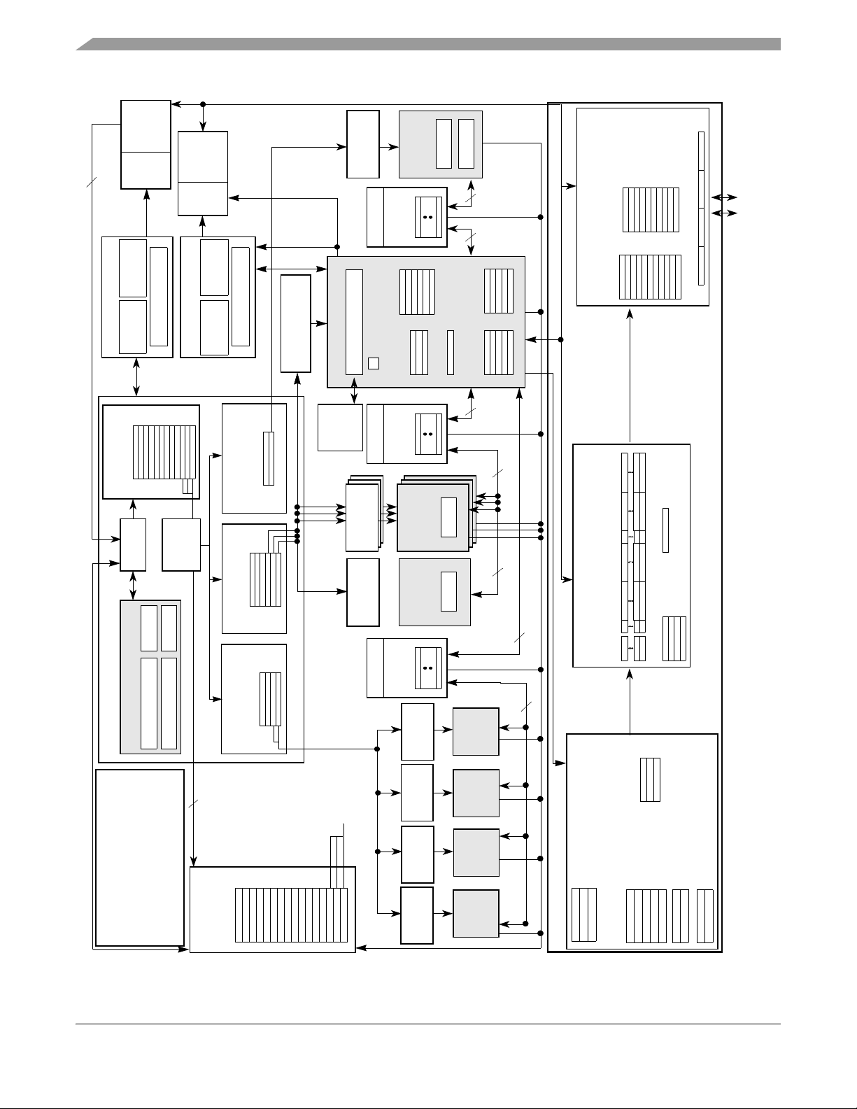
Figure 1 shows a block diagram of the MPC7448. The core
is a high-performance superscalar design supporting a
double-precision floating-point unit and a SIMD multimedia
unit. The memory storage subsystem supports the MPX bus
protocol and a subset of the 60x bus protocol to main
memory and other system resources.
© Freescale Semiconductor, Inc., 2005. All rights reserved.
Page 2
Overview
128-Bit (4 Instructions)
Instruction MMU
Instruction Unit
1
I Cache
32-Kbyte
Stations (2)
D Cache
IBAT Array
LR
32-Kbyte
Data MMU
Unit
Dispatch
Tags
128-Entry
SRs
DTLB
(Original)
GPR Issue
DBAT Array
(6-Entry/3-Issue) (4-Entry/2-Issue) (2-Entry/1-Issue)
EA
Reservation
Stations (2-Entry)
Tags
ITLB
128-Entry
SRs
(Shadow)
(12-Word)
Instruction Queue
Fetcher
CTR
Reservation
FPR File
Vector Touch Engine
Reservation
Reservation
Reservation
Reservation
(EA Calculation)
+
GPR File
Station
Station
Station
Stations (2)
VR File
16 Rename
L1 Castout
Finished
16 Rename
16 Rename
PA
Load/Store Unit
Touch
Vec to r
Queue
+ x ÷
FPSCR
Unit 2
(3)
FPSCR
L1 Push
Completed
+
+
+
x ÷
64-Bit
64-Bit
Load Miss
Stores
32-Bit
32-Bit
32-Bit
Push
Queue (6)
Castout
Queue (5) /
Bus Store Queue
System Bus Interface
Load
Queue (11)
Snoop Push/
Interventions
Block 1 (32-Byte)
Status
L2 Store Queue (L2SQ)
(4)
L1 Castouts
Block 0 (32-Byte)
Status
128-Bit
1-Mbyte Unified L2 Cache Controller
Line
Ta gs
Bus Accumulator
64-Bit
36-Bit
Data Bus
Address Bus
Floating-
Point Unit
Buffers
Stores
Buffers
Integer
Unit 2
Integer
Integer
Unit 2 Unit 1
Integer
Buffers
Additional Features
Branch Processing Unit
BTIC (128-Entry)
BHT (2048-Entry)
• Time Base Counter/Decrementer
• Clock Multiplier
• JTAG/COP Interface
• Thermal/Power Management
• Performance Monitor
• Out-of-Order Issue of AltiVec Instr.
VR Issue FPR Issue
96-Bit (3 Instructions)
(16-Entry)
Completion Unit
Completion Queue
Station
Reservation
Station
Completes up
to three
per clock
instructions
Reservation
Station
Reservation
Station
Reservation
Vect or
Vector
Vector
Vector
Integer
Integer
Permute
FPU
Unit 1
Unit 2
Unit
128-Bit
Queues
L1 Service
L1 Store Queue
(LSQ)
Memory Subsystem
L1 Load Miss (5)
L2 Prefetch (3)
Instruction Fetch (2)
Cacheable Store Miss (2)
The Castout Queue itself is limited to 5 entries, ensuring 1 entr y will be available for a push.
The Castout Queue and Push Queue share resources such for a combined total of 6 entries.
L1 Load Queue (LLQ)
Notes:
Figure 1. MPC7448 Block Diagram
MPC7448 RISC Microprocessor Hardware Specifications, Rev. 1
2 Freescale Semiconductor
Page 3

2Features
This section summarizes features of the MPC7448 implementation of the PowerPC architecture.
Major features of the MPC7448 are as follows:
• High-performance, superscalar microprocessor
— Up to four instructions can be fetched from the instruction cache at a time.
— Up to three instructions plus a branch instruction can be dispatched to the issue queues at a
time.
— Up to 12 instructions can be in the instruction queue (IQ).
— Up to 16 instructions can be at some stage of execution simultaneously.
— Single-cycle execution for most instructions
— One instruction per clock cycle throughput for most instructions
— Seven-stage pipeline control
• Eleven independent execution units and three register files
— Branch processing unit (BPU) features static and dynamic branch prediction
– 128-entry (32-set, four-way set-associative) branch target instruction cache (BTIC), a cache
of branch instructions that have been encountered in branch/loop code sequences. If a target
instruction is in the BTIC, it is fetched into the instruction queue a cycle sooner than it can
be made available from the instruction cache. T ypically, a fetch that hits the BTIC provides
the first four instructions in the target stream.
– 2048-entry branch history table (BHT) with 2 bits per entry for four levels of
prediction—not taken, strongly not taken, taken, and strongly taken
– Up to three outstanding speculative branches
– Branch instructions that do not update the count register (CTR) or link register (LR) are
often removed from the instruction stream.
– Eight-entry link register stack to predict the target address of Branch Conditional to Link
Register (bclr) instructions
Features
— Four integer units (IUs) that share 32 GPRs for integer operands
– Three identical IUs (IU1a, IU1b, and IU1c) can execute all integer instructions except
multiply, divide, and move to/from special-purpose register instructions.
– IU2 executes miscellaneous instructions, including the CR logical operations, integer
multiplication and division instructions, and move to/from special-purpose register
instructions.
— Five-stage FPU and 32-entry FPR file
– Fully IEEE 754-1985–compliant FPU for both single- and double-precision operations
– Supports non-IEEE mode for time-critical operations
– Hardware support for denormalized numbers
– Thirty-two 64-bit FPRs for single- or double-precision operands
MPC7448 RISC Microprocessor Hardware Specifications, Rev. 1
Freescale Semiconductor 3
Page 4

Features
— Four vector units and 32-entry vector register file (VRs)
– Vector permute unit (VPU)
– Vecto r integer unit 1 (VIU1) handles short-latency AltiVec™ integer instructions, such as vector add
instructions (for example, vaddsbs, vaddshs, and vaddsws).
– Vector integer unit 2 (VIU2) handles longer-latency AltiVec integer instructions, such as vector
multiply add instructions (for example, vmhaddshs, vmhraddshs, and vmladduhm).
– Vector floating-point unit (VFPU)
— Three-stage load/store unit (LSU)
– Supports integer, floating-point, and vector instruction load/store traffic
– Four-entry vector touch queue (VTQ) supports all four architected AltiVec data stream
operations
– Three-cycle GPR and AltiVec load latency (byte, half word, word, vector) with one-cycle
throughput
– Four-cycle FPR load latency (single, double) with one-cycle throughput
– No additional delay for misaligned access within double-word boundary
– A dedicated adder calculates effective addresses (EAs).
– Supports store gathering
– Performs alignment, normalization, and precision conversion for floating-point data
– Executes cache control and TLB instructions
– Performs alignment, zero padding, and sign extension for integer data
– Supports hits under misses (multiple outstanding misses)
– Supports both big- and little-endian modes, including misaligned little-endian accesses
• Three issue queues, FIQ, VIQ, and GIQ, can accept as many as one, two, and three instructions,
respectively, in a cycle. Instruction dispatch requires the following:
— Instructions can only be dispatched from the three lowest IQ entries—IQ0, IQ1, and IQ2.
— A maximum of three instructions can be dispatched to the issue queues per clock cycle.
— Space must be available in the CQ for an instruction to dispatch (this includes instructions that
are assigned a space in the CQ but not in an issue queue).
• Rename buffers
— 16 GPR rename buffers
— 16 FPR rename buffers
— 16 VR rename buffers
• Dispatch unit
— Decode/dispatch stage fully decodes each instruction
• Completion unit
— Retires an instruction from the 16-entry completion queue (CQ) when all instructions ahead of
it have been completed, the instruction has finished executing, and no exceptions are pending
— Guarantees sequential programming model (precise exception model)
— Monitors all dispatched instructions and retires them in order
MPC7448 RISC Microprocessor Hardware Specifications, Rev. 1
4 Freescale Semiconductor
Page 5

— Tracks unresolved branches and flushes instructions after a mispredicted branch
— Retires as many as three instructions per clock cycle
• Separate on-chip L1 instruction and data caches (Harvard architecture)
— 32-Kbyte, eight-way set-associative instruction and data caches
— Pseudo least-recently-used (PLRU) replacement algorithm
— 32-byte (eight-word) L1 cache block
— Physically indexed/physical tags
— Cache write-back or write-through operation programmable on a per-page or per-block basis
— Instruction cache can provide four instructions per clock cycle; data cache can provide four
words per clock cycle
— Caches can be disabled in software.
— Caches can be locked in software.
— MESI data cache coherency maintained in hardware
— Separate copy of data cache tags for efficient snooping
— Parity support on cache
— No snooping of instruction cache except for icbi instruction
Features
— Data cache supports AltiVec LRU and transient instructions
— Critical double- and/or quad-word forwarding is performed as needed. Critical quad-word
forwarding is used for AltiVec loads and instruction fetches. Other accesses use critical
double-word forwarding.
• Level 2 (L2) cache interface
— On-chip, 1-Mbyte, eight-way set-associative unified instruction and data cache
— Cache write-back or write-through operation programmable on a per-page or per-block basis
— Parity support on cache tags
— ECC or parity support on data
— Error injection allows testing of error recovery software
• Separate memory management units (MMUs) for instructions and data
— 52-bit virtual address, 32- or 36-bit physical address
— Address translation for 4-Kbyte pages, variable-sized blocks, and 256-Mbyte segments
— Memory programmable as write-back/write-through, caching-inhibited/caching-allowed, and
memory coherency enforced/memory coherency not enforced on a page or block basis
— Separate IBATs and DBATs (eight each) also defined as SPRs
— Separate instruction and data translation lookaside buffers (TLBs)
– Both TLBs are 128-entry, two-way set-associative and use an LRU replacement algorithm.
– TLBs are hardware- or software-reloadable (that is, a page table search is performed in
hardware or by system software on a TLB miss).
MPC7448 RISC Microprocessor Hardware Specifications, Rev. 1
Freescale Semiconductor 5
Page 6

Features
• Efficient data flow
— Although the VR/LSU interface is 128 bits, the L1/L2 bus interface allows up to 256 bits.
— The L1 data cache is fully pipelined to provide 128 bits/cycle to or from the VRs.
— The L2 cache is fully pipelined to provide 32 bytes per clock every other cycle to the L1 caches.
— As many as 16 out-of-order transactions can be present on the MPX bus.
— Store merging for multiple store misses to the same line. Only coherency action taken
(address-only) for store misses merged to all 32 bytes of a cache block (no data tenure needed).
— Three-entry finished store queue and five-entry completed store queue between the LSU and
the L1 data cache
— Separate additional queues for efficient buffering of outbound data (such as castouts and
write-through stores) from the L1 data cache and L2 cache
• Multiprocessing support features include the following:
— Hardware-enforced, MESI cache coherency protocols for data cache
— Load/store with reservation instruction pair for atomic memory references, semaphores, and
other multiprocessor operations
• Power and thermal management
— Dynamic frequency switching (DFS) feature allows processor core frequency to be halved or
quartered through software to reduce power consumption.
— The following three power-saving modes are available to the system:
– Nap—Instruction fetching is halted. Only the clocks for the time base, decrementer, and
JTAG logic remain running. The part goes into the doze state to snoop memory operations
on the bus and then back to nap using a QREQ/QACK processor-system handshake
protocol.
– Sleep—Power consumption is further reduced by disabling bus snooping, leaving only the
PLL in a locked and running state. All internal functional units are disabled.
– Deep sleep—When the part is in the sleep state, the system can disable the PLL. The system
can then disable the SYSCLK source for greater system power savings. Power-on reset
procedures for restarting and relocking the PLL must be followed upon exiting the deep
sleep state.
— Instruction cache throttling provides control of instruction fetching to limit device temperature.
— A new temperature diode that can determine the temperature of the microprocessor
— Support for core voltage derating to further reduce power consumption
• Performance monitor can be used to help debug system designs and improve software efficiency.
• In-system testability and debugging features through JTAG boundary-scan capability
• Testability
— LSSD scan design
— IEEE 1149.1 JTAG interface
MPC7448 RISC Microprocessor Hardware Specifications, Rev. 1
6 Freescale Semiconductor
Page 7
Comparison with the MPC7447A, MPC7447, MPC7445, and MPC7441
• Reliability and serviceability
— Parity checking on system bus
— Parity checking on the L1 caches and L2 data tags
— ECC or parity checking on L2 data
3 Comparison with the MPC7447A, MPC7447, MPC7445,
and MPC7441
Table 1 compares the key features of the MPC7448 with the key features of the earlier MPC7447A,
MPC7447, MPC7445, and MPC7441. All are based on the MPC7450 RISC microprocessor and are
architecturally very similar. The MPC7448 is identical to the MPC7447A, but the MPC7448 supports 1
Mbyte of L2 cache with ECC and the use of dynamic frequency switching (DFS) with more bus-to-core
ratios.
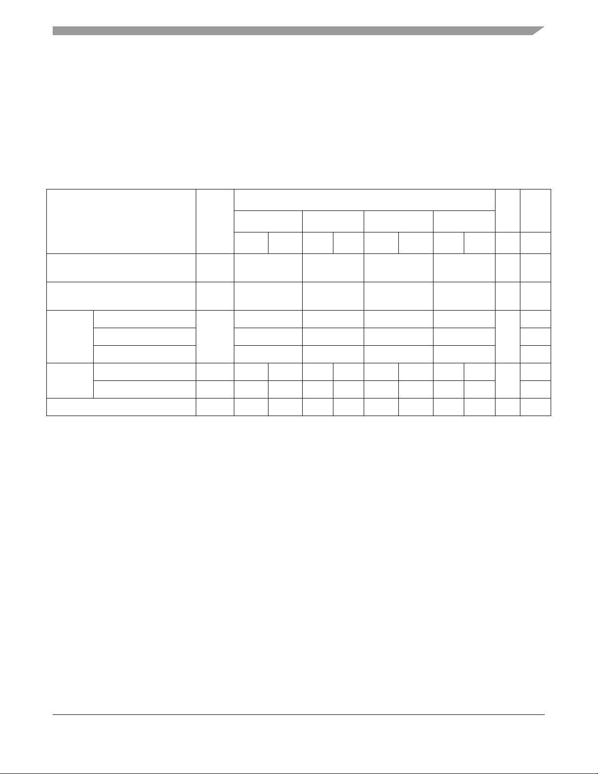
Table 1. Microarchitecture Comparison
Microarchitectural Specs MPC7448 MPC7447A MPC7447 MPC7445 MPC7441
Basic Pipeline Functions
Logic inversions per cycle 18
Pipeline stages up to execute 5
Total pipeline stages (minimum) 7
Pipeline maximum instruction throughput 3 + branch
Pipeline Resources
Instruction buffer size 12
Completion buffer size 16
Renames (integer, float, vector) 16, 16, 16
Maximum Execution Throughput
SFX 3
Vector 2 (any 2 of 4 units)
Scalar floating-point 1
Out-of-Order Window Size in Execution Queues
SFX integer units 1 entry × 3 queues
Vector units In order, 4 queues
Scalar floating-point unit In order
Branch Processing Resources
Prediction structures BTIC, BHT, link stack
BTIC size, associativity 128-entry, 4-way
BHT size 2K-entry
Link stack depth 8
Unresolved branches supported 3
Branch taken penalty (BTIC hit) 1
Minimum misprediction penalty 6
MPC7448 RISC Microprocessor Hardware Specifications, Rev. 1
Freescale Semiconductor 7
Page 8
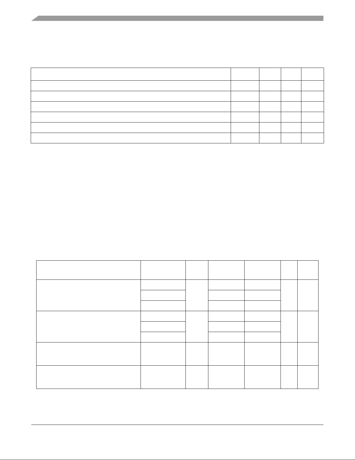
Comparison with the MPC7447A, MPC7447, MPC7445, and MPC7441
Table 1. Microarchitecture Comparison (continued)
Microarchitectural Specs MPC7448 MPC7447A MPC7447 MPC7445 MPC7441
Execution Unit Timings (Latency-Throughput)
Aligned load (integer, float, vector) 3-1, 4-1, 3-1
Misaligned load (integer, float, vector) 4-2, 5-2, 4-2
L1 miss, L2 hit latency with ECC (data/instruction) 12/16 —
L1 miss, L2 hit latency without ECC (data/instruction) 11/15 9/13
SFX (add, sub, shift, rot, cmp, logicals) 1-1
Integer multiply (32 × 8, 32 × 16, 32 × 32) 4-1, 4-1, 5-2
Scalar float 5-1
VSFX (vector simple) 1-1
VCFX (vector complex) 4-1
VFPU (vector float) 4-1
VPER (vector permute) 2-1
MMUs
TLBs (instruction and data) 128-entry, 2-way
Tablewalk mechanism Hardware + software
Instruction BATs/data BATs 8/8 8/8 8/8 8/8 4/4
L1 I Cache/D Cache Features
Size 32K/32K
Associativity 8-way
Locking granularity Way
Parity on I cache Word
Parity on D cache Byte
Number of D cache misses (load/store) 5/2 5/1
Data stream touch engines 4 streams
On-Chip Cache Features
Cache level L2
Size/associativity 1-Mbyte/
512-Kbyte/8-way 256-Kbyte/8-way
8-way
Access width 256 bits
Number of 32-byte sectors/line 2 2
Parity tag Byte Byte
Parity data Byte Byte
Data ECC 64-bit —
Thermal Control
Dynamic frequency switching divide-by-two mode Yes Yes No No No
Dynamic frequency switching divide-by-four mode Yes No No No No
Thermal diode Yes Yes No No No
MPC7448 RISC Microprocessor Hardware Specifications, Rev. 1
8 Freescale Semiconductor
Page 9
General Parameters
4 General Parameters
The following list summarizes the general parameters of the MPC7448:
Technology 90 nm CMOS SOI, nine-layer metal
Die size 8.0 mm × 7.3 mm
Transistor count 90 million
Logic design Mixed static and dynamic
Packages Surface mount 360 ceramic ball grid array (HCTE)
Surface mount 360 ceramic land grid array (HCTE)
Surface mount 360 ceramic ball grid array with lead-free spheres (HCTE)
Core power supply 1.30 V (1700 MHz device)
1.25 V (1600 MHz device)
1.20 V (1420 MHz device)
1.15 V (1000 MHz device)
I/O power supply 1.5 V, 1.8 V, or 2.5 V
5 Electrical and Thermal Characteristics
This section provides the AC and DC electrical specifications and thermal characteristics for the
MPC7448.
5.1 DC Electrical Characteristics
The tables in this section describe the MPC7448 DC electrical characteristics. Table 2 provides the
absolute maximum ratings. See Section 9.2, “Power Supply Design and Sequencing” for power
sequencing requirements.
Table 2. Absolute Maximum Ratings
Characteristic Symbol Maximum Value Unit Notes
Core supply voltage V
PLL supply voltage AV
Processor bus supply voltage I/O Voltage Mode = 1.5 V OV
I/O Voltage Mode = 1.8 V –0.3 to 2.2 3
I/O Voltage Mode = 2.5 V –0.3 to 3.0 3
Input voltage Processor bus V
JTAG signals V
Storage temperature range T
Notes:
1. Functional and tested operating conditions are given in Ta b le 4 . Absolute maximum ratings are stress ratings only and
functional operation at the maximums is not guaranteed. Stresses beyond those listed may affect device reliability or cause
permanent damage to the device.
2. See Section 9.2, “Power Supply Design and Sequencing” for power sequencing requirements.
3. Bus must be configured in the corresponding I/O voltage mode; see Ta b le 3 .
4. Caution: Vin must not exceed OV
the overshoot specifications. V
by more than 0.3 V at any time including during power-on reset except as allowed by
DD
may overshoot/undershoot to a voltage and for a maximum duration as shown in Figure 2.
in
DD
DD
DD
in
in
stg
1
–0.3 to 1.4 V 2
–0.3 to 1.4 V 2
–0.3 to 1.8 V 3
–0.3 to OVDD + 0.3 V 4
–0.3 to OVDD + 0.3 V
– 55 to 150 °C
MPC7448 RISC Microprocessor Hardware Specifications, Rev. 1
Freescale Semiconductor 9
Page 10
Electrical and Thermal Characteristics
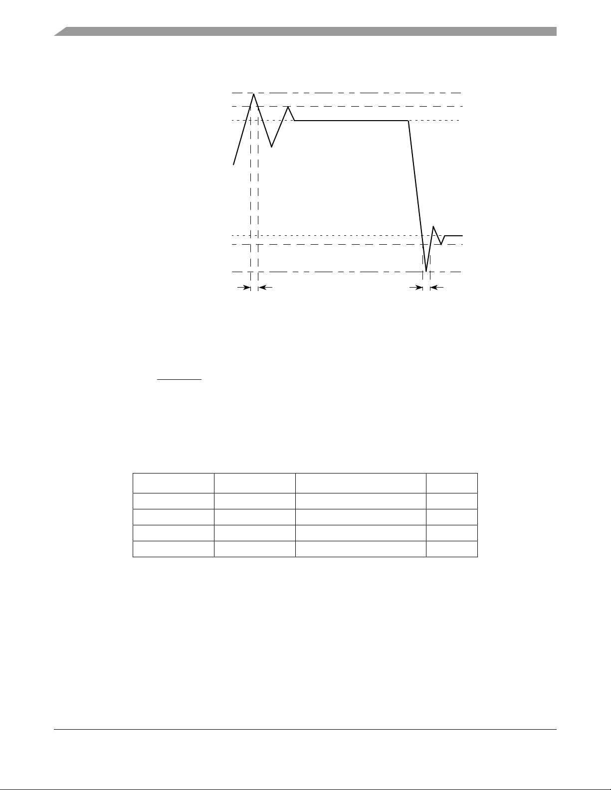
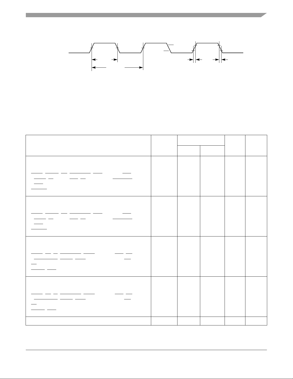
Figure 2 shows the undershoot and overshoot voltage on the MPC7448.
OVDD + 20%
OVDD + 5%
OV
DD
V
IH
V
IL
GND
GND – 0.3 V
GND – 0.7 V
Not to Exceed 10%
of t
SYSCLK
Figure 2. Overshoot/Undershoot Voltage
The MPC7448 provides several I/O voltages to support both compatibility with existing systems and
migration to future systems. The MPC7448 core voltage must always be provided at the nominal voltage
(see Table 4) or at the supported derated voltage (see Section 5.3, “Voltage and Frequency Derating”). The
input voltage threshold for each bus is selected by sampling the state of the voltage select pins at the
negation of the signal HRESET . The output voltage will swing from GND to the maximum voltage applied
to the OVDD power pins. Table 3 provides the input threshold voltage settings. Because these settings may
change in future products, it is recommended that BVSEL[0:1] be configured using resistor options,
jumpers, or some other flexible means, with the capability to reconfigure the termination of this signal in
the future, if necessary.
Table 3. Input Threshold Voltage Setting
BVSEL0 BVSEL1 I/O Voltage Mode
0 0 1.8 V 2, 3
0 1 2.5 V 2, 4
1 0 1.5 V 2
1 1 2.5 V 4
Notes:
1. Caution: The I/O voltage mode selected must agree with the OV
supplied. See Ta bl e 4 .
2. If used, pull-down resistors should be less than 250 Ω.
3. The pin configuration used to select 1.8V mode on the MPC7448 is not compatible
with the pin configuration used to select 1.8V mode on the MPC7447A and earlier
devices.
4. The pin configuration used to select 2.5V mode on the MPC7448 is fully compatible
with the pin configuration used to select 2.5V mode on the MPC7447A and earlier
devices.
MPC7448 RISC Microprocessor Hardware Specifications, Rev. 1
10 Freescale Semiconductor
1
DD
Notes
voltages
Page 11
Electrical and Thermal Characteristics
Table 4 provides the recommended operating conditions for the MPC7448 part numbers described by this
document; see Section 11.1, “Part Numbers Fully Addressed by This Document,” for more information.
See Section 9.2, “Power Supply Design and Sequencing” for power sequencing requirements.
NOTE
Table 4 describes the nominal operating conditions of the device. For
information on the operation of the device at supported derated core voltage
conditions, see Section 5.3, “Voltage and Frequency Derating.”
Table 4. Recommended Operating Conditions
Characteristic Symbol
Recommended Value
1000 MHz 1420 MHz 1600 MHz 1700 MHz
Min Max Min Max Min Max Min Max
1
Unit Notes
Core supply voltage V
1.15 V ± 50 mV 1.2 V ± 50 mV 1.25 V ± 50 mV 1.3 V +20/
DD
V 3, 4, 5
–50mV
PLL supply voltage AV
1.15 V ± 50 mV 1.2 V ± 50 mV 1.25 V ± 50 mV 1.3 V +20/
DD
V 2, 3, 4
–50mV
Processor
bus
supply
voltage
Input
voltage
I/O Voltage Mode = 1.5 V OV
I/O Voltage Mode = 1.8 V 1.8 V ± 5% 1.8 V ± 5% 1.8 V ± 5% 1.8 V ± 5% 4
I/O Voltage Mode = 2.5 V 2.5 V ± 5% 2.5 V ± 5% 2.5 V ± 5% 2.5 V ± 5% 4
Processor bus V
JTAG signals V
Die-junction temperature T
DD
in
in
j
1.5 V ± 5% 1.5 V ± 5% 1.5 V ± 5% 1.5 V ± 5% V 4
GND OV
GND OV
DD
DD
GND OV
GND OV
DD
DD
GND OV
GND OV
DD
DD
GND OV
GND OV
DD
DD
V
0 105 0 105 0 105 0 105 °C
Notes:
1. These are the recommended and tested operating conditions. Some speed grades in addition support voltage derating; see
Section 5.3, “Voltage and Frequency Derating.” Proper device operation outside of these conditions and those specified in
Section 5.3 is not guaranteed.
2. This voltage is the input to the filter discussed in Section 9.2.2, “PLL Power Supply Filtering,” and not necessarily the voltage at
the AV
3. V
pin, which may be reduced from VDD by the filter.
DD
and AVDD may be reduced for some speed grades in order to reduce power consumption if further maximum core
DD
frequency constraints are observed. See Section 5.3, “Voltage and Frequency Derating,” for specific information.
4. Caution: Power sequencing requirements must be met; see Section 9.2, “Power Supply Design and Sequencing”.
5. Caution: See Section 9.2.3, “Transient Specifications” for information regarding transients on this power supply.
MPC7448 RISC Microprocessor Hardware Specifications, Rev. 1
Freescale Semiconductor 11
Page 12
Electrical and Thermal Characteristics
Table 5 provides the package thermal characteristics for the MPC7448. For more information regarding
thermal management, see Section 9.7, “Thermal Management Information.”
Table 5. Package Thermal Characteristics
Characteristic Symbol Value Unit Notes
1
Junction-to-ambient thermal resistance, natural convection, single-layer (1s) board R
Junction-to-ambient thermal resistance, natural convection, four-layer (2s2p) board R
Junction-to-ambient thermal resistance, 200 ft/min airflow, single-layer (1s) board R
Junction-to-ambient thermal resistance, 200 ft/min airflow, four-layer (2s2p) board R
Junction-to-board thermal resistance R
Junction-to-case thermal resistance R
θ
θ
θ
θ
JA
θ
JMA
JMA
JMA
JB
θ
JC
26 °C/W 2, 3
19 °C/W 2, 4
22 °C/W 2, 4
16 °C/W 2, 4
11 °C/W 5
< 0.1 °C/W 6
Notes:
1. Refer to Section 9.7, “Thermal Management Information,” for details about thermal management.
2. Junction temperature is a function of on-chip power dissipation, package thermal resistance, mounting site (board)
temperature, ambient temperature, airflow, power dissipation of other components on the board, and board thermal
resistance.
3. Per JEDEC JESD51-2 with the single-layer board horizontal
4. Per JEDEC JESD51-6 with the board horizontal
5. Thermal resistance between the die and the printed-circuit board per JEDEC JESD51-8. Board temperature is measured on
the top surface of the board near the package.
6. This is the thermal resistance between die and case top surface as measured by the cold plate method (MIL SPEC-883
Method 1012.1) with the calculated case temperature. The actual value of R
for the part is less than 0.1°C/W.
θJC
Table 6 provides the DC electrical characteristics for the MPC7448.
Table 6. DC Electrical Specifications
At recommended operating conditions. See Ta bl e 4 .
Characteristic
Input high voltage
(all inputs)
Nominal Bus
Volt ag e
1.5 V
Symbol Min Max Unit Notes
1
OVDD × 0.65 OVDD + 0.3 V 2
IH
1.8 OVDD × 0.65 OVDD + 0.3
2.5 1.7 OVDD + 0.3
Input low voltage
(all inputs)
1.5 V
IL
–0.3 OVDD × 0.35 V 2
1.8 –0.3 OVDD × 0.35
2.5 –0.3 0.7
Input leakage current,
V
= GVDD/OVDD
in
= GND
V
in
High-impedance (off-state) leakage current,
= GVDD/OVDD
V
in
= GND
V
in
—I
—I
in
TSI
—
—
µA 2, 3
50
– 50
µA 2, 3, 4
50
– 50
MPC7448 RISC Microprocessor Hardware Specifications, Rev. 1
12 Freescale Semiconductor
Page 13
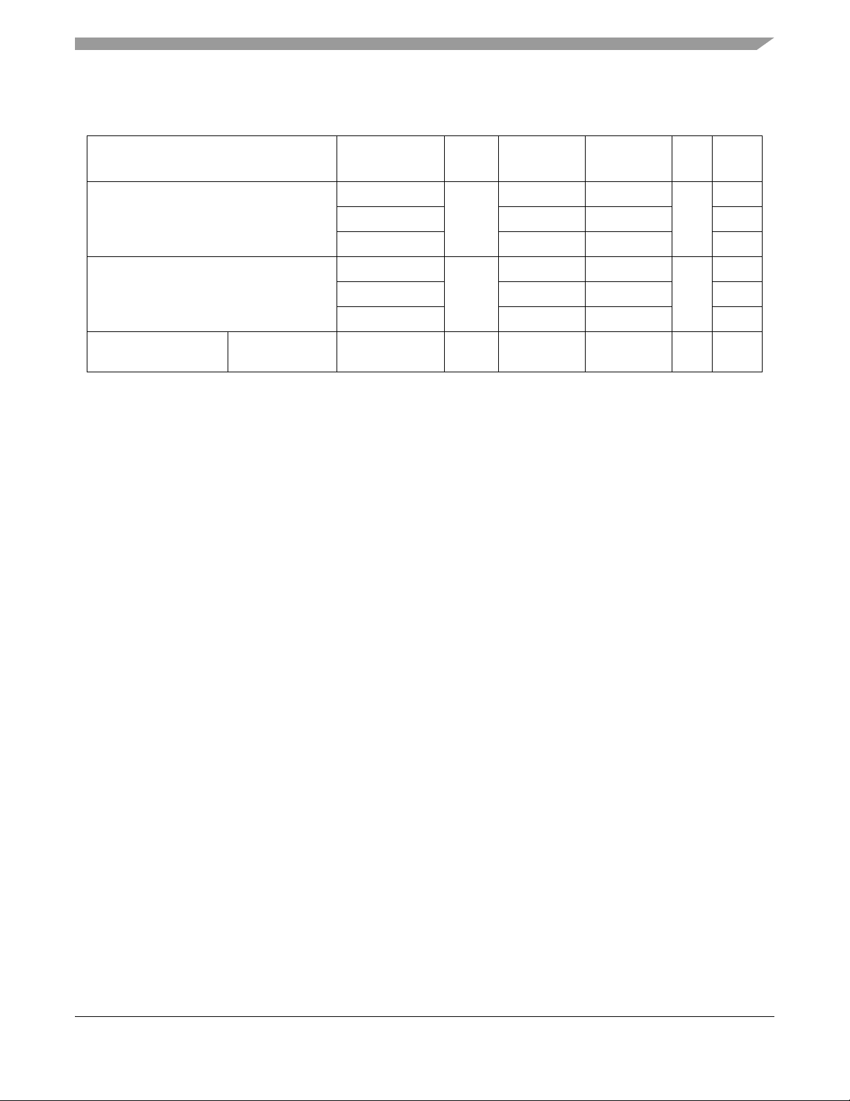
Table 6. DC Electrical Specifications (continued)
At recommended operating conditions. See Ta bl e 4 .
Electrical and Thermal Characteristics
Characteristic
Output high voltage @ IOH = –5 mA 1.5 V
Output low voltage @ I
Capacitance,
0 V, f = 1 MHz
V
=
in
Notes:
1. Nominal voltages; see Ta b le 4 for recommended operating conditions.
2. All I/O signals are referenced to OV
3. Excludes test signals and IEEE 1149.1 boundary scan (JTAG) signals
4. The leakage is measured for nominal OV
example, both OVDD and VDD vary by either +5% or –5%).
5. Capacitance is periodically sampled rather than 100% tested.
5 mA 1.5 V
=
OL
All inputs C
DD
Nominal Bus
Volt ag e
1.8 OVDD – 0.45 —
2.5 1.8 —
1.8 — 0.45
2.5 — 0.6
.
and VDD, or both OVDD and VDD must vary in the same direction (for
DD
Symbol Min Max Unit Notes
1
OVDD – 0.45 — V
OH
OL
in
—0.45V
—8.0pF5
Table 7 provides the power consumption for the MPC7448 part numbers described by this document; see
Section 11.1, “Part Numbers Fully Addressed by This Document,” for more information. The MPC7448
RISC Microprocessor Hardware Specifications presents guidelines on the use of these parameters for
system design. For information on power consumption when dynamic frequency switching is enabled, see
Section 9.7.5, “Dynamic Frequency Switching (DFS).” Several power specifications are provided for
Full-Power mode. The Nominal – T ypical value represents the sustained power consumption of the device
when running a typical benchmark at temperatures in a typical system. The Nominal – Thermal value is
intended to represent the sustained power consumption of the device when running a typical code sequence
at high temperature and is recommended to be used as the basis for designing a thermal solution; see
Section 9.7, “Thermal Management Information” for more information on thermal solutions. The
Maximum value is recommended to be used for power supply design because this represents the maximum
peak power draw of the device that a power supply must be capable of sourcing without voltage droop.
NOTE
The power consumption information in this table applies when the device
operates at the nominal core voltage indicated in Table 4. For power
consumption at derated core voltage conditions, see Section 5.3, “Voltage
and Frequency Derating.”
MPC7448 RISC Microprocessor Hardware Specifications, Rev. 1
Freescale Semiconductor 13
Page 14
Electrical and Thermal Characteristics
Table 7. Power Consumption for MPC7448
Die Junction
Temperature
(Tj)
Typical – Nominal 65 °C 15.0 19.0 20.0 21.0 W 1, 2
Typical – Thermal 105 °C 18.6 23.3 24.4 25.6 W 1, 5
Maximum 105 °C 21.6 27.1 28.4 29.8 W 1, 3
Typical 105 °C 11.1 11.8 13.0 13.0 W 1, 6
Typical 105 °C 10.8 11.4 12.5 12.5 W 1, 6
Typical 105 °C 10.4 11.0 12.0 12.0 W 1, 6
Notes:
1. These values specify the power consumption for the core power supply (V
processor bus frequencies and configurations. The values do not include I/O supply power (OVDD) or PLL supply power
). OVDD power is system dependent but is typically < 5% of VDD power. Worst case power consumption for
(AV
DD
AVDD<13mW.
2. Typical nominal power consumption is an average value measured at the nominal recommended V
while running the Dhrystone 2.1 benchmark and achieving 2.3 Dhrystone MIPs/MHz. This parameter is not 100% tested but
periodically sampled.
3. Maximum power consumption is the average measured at nominal V
Ta bl e 4 ) while running an entirely cache-resident, contrived sequence of instructions to keep all the execution units maximally
busy.
4. Doze mode is not a user-definable state; it is an intermediate state between full-power and either nap or sleep mode. As a
result, power consumption for this mode is not tested.
5. Typical thermal power consumption is an average value measured at the nominal recommended V
105 °C while running the Dhrystone 2.1 benchmark and achieving 2.3 Dhrystone MIPs/MHz. This parameter is not 100%
tested but periodically sampled.
6. Typical power consumption for these modes is measured at the nominal recommended V
mode described. This parameter is not 100% tested but is periodically sampled.
1000 MHz 1420 MHz 1600 MHz 1700 MHz
Deep Sleep Mode (PLL Disabled)
Processor (CPU) Frequency
Full-Power Mode
Nap Mode
Sleep Mode
DD
and maximum operating junction temperature (see
DD
Unit Notes
) at nominal voltage and apply to all valid
(see Ta bl e 4 ) and 65°C
DD
(see Ta b le 4 ) and
DD
(see Ta bl e 4 ) and 105 °C in the
DD
5.2 AC Electrical Characteristics
This section provides the AC electrical characteristics for the MPC7448. After fabrication, functional parts
are sorted by maximum processor core frequency as shown in Section 5.2.1, “Clock AC Specifications,”
and tested for conformance to the AC specifications for that frequency. The processor core frequency,
determined by the bus (SYSCLK) frequency and the settings of the PLL_CFG[0:5] signals, can be
dynamically modified using dynamic frequency switching (DFS). Parts are sold by maximum processor
core frequency; see Section 11, “Part Numbering and Marking,” for information on ordering parts. DFS is
described in Section 9.7.5, “Dynamic Frequency Switching (DFS).”
MPC7448 RISC Microprocessor Hardware Specifications, Rev. 1
14 Freescale Semiconductor
Page 15
Electrical and Thermal Characteristics
5.2.1 Clock AC Specifications
Table 8 provides the clock AC timing specifications as defined in Figure 3 and represents the tested
operating frequencies of the devices. The maximum system bus frequency, f
SYSCLK
considered a practical maximum in a typical single-processor system. This does not exclude
multi-processor systems, but these typically require considerably more design effort to achieve the
maximum rated bus frequency. The actual maximum SYSCLK frequency for any application of the
MPC7448 will be a function of the AC timings of the microprocessor(s), the AC timings for the system
controller, bus loading, printed-circuit board topology , trace lengths, and so forth, and may be less than the
value given in Table 8.
NOTE
The core frequency information in this table applies when the device operates at
the nominal core voltage indicated in
Table 4. For core frequency
specifications at derated core voltage conditions, see Section 5.3, “Voltage
and Frequency Derating.”
Table 8. Clock AC Timing Specifications
At recommended operating conditions. See Ta bl e 4 .
Maximum Processor Core Frequency
, given in Table 8, is
Characteristic Symbol
Min Max Min Max Min Max Min Max
Processor
core
frequency
VCO frequency f
SYSCLK frequency f
SYSCLK cycle time t
SYSCLK rise and fall time tKR, t
SYSCLK duty cycle measured at
OV
DD
SYSCLK cycle-to-cycle jitter — 150 — 150 — 150 — 150 ps 5, 6
DFS mode disabled f
DFS mode enabled f
/2
core
core_DF
VCO
SYSCLK
SYSCLK
t
KHKL
t
SYSCLK
600 1000 600 1420 600 1600 600 1700 MHz 1, 8, 9
300 500 300 710 300 800 300 850 10
600 1000 600 1420 600 800 600 1700 MHz 1, 9, 11
33 200 33 200 33 200 33 200 MHz 1, 2, 8
5.0305.0305.0305.030ns 2
—0.5—0.5—0.5—0.5ns 3
KF
/
40 60 40 60 40 60 40 60 % 4
Unit Notes1000 MHz 1420 MHz 1600 MHz 1700 MHz
MPC7448 RISC Microprocessor Hardware Specifications, Rev. 1
Freescale Semiconductor 15
Page 16
Electrical and Thermal Characteristics
Table 8. Clock AC Timing Specifications (continued)
At recommended operating conditions. See Ta bl e 4 .
Maximum Processor Core Frequency
Characteristic Symbol
Unit Notes1000 MHz 1420 MHz 1600 MHz 1700 MHz
Min Max Min Max Min Max Min Max
Internal PLL relock time — 100 — 100 — 100 — 100 µs7
Notes:
1. Caution: The SYSCLK frequency and PLL_CFG[0:5] settings must be chosen such that the resulting SYSCLK (bus)
frequency, processor core frequency, and PLL (VCO) frequency do not exceed their respective maximum or minimum
operating frequencies. Refer to the PLL_CFG[0:5] signal description in Section 9.1.1, “PLL Configuration,” for valid
PLL_CFG[0:5] settings.
2. Actual maximum system bus frequency is system-dependent. See Section 5.2.1, “Clock AC Specifications.”
3. Rise and fall times for the SYSCLK input measured from 0.4 to 1.4 V
4. Timing is guaranteed by design and characterization.
5. Guaranteed by design
6. The SYSCLK driver’s closed loop jitter bandwidth should be less than 1.5 MHz at –3 dB.
7. Relock timing is guaranteed by design and characterization. PLL-relock time is the maximum amount of time required for PLL
lock after a stable V
and SYSCLK are reached during the power-on reset sequence. This specification also applies when
DD
the PLL has been disabled and subsequently re-enabled during sleep mode. Also note that HRESET must be held asserted
for a minimum of 255 bus clocks after the PLL-relock time during the power-on reset sequence.
8. This reflects the maximum and minimum core frequencies when the dynamic frequency switching feature (DFS) is disabled.
f
core_DFS
provides the maximum and minimum core frequencies when operating in a DFS mode.
9. Caution: These values specify the maximum processor core and VCO frequencies when the device is operated at the
nominal core voltage. If operating the device at the derated core voltage, the processor core and VCO frequencies must be
reduced. See Section 5.3, “Voltage and Frequency Derating,” for more information.
10.This specification supports the Dynamic Frequency Switching (DFS) feature and is applicable only when one of the DFS
modes (divide-by-2 or divide-by-4) is enabled. When DFS is disabled, the core frequency must conform to the maximum and
minimum frequencies stated for f
core
.
11.Use of the DFS feature does not affect VCO frequency.
MPC7448 RISC Microprocessor Hardware Specifications, Rev. 1
16 Freescale Semiconductor
Page 17
Electrical and Thermal Characteristics
Figure 3 provides the SYSCLK input timing diagram.
CV
SYSCLK
V
M
CV
IL
t
SYSCLK
V
M
V
M
t
KHKL
IH
t
KR
t
KF
VM = Midpoint Voltage (OVDD/2)
Figure 3. SYSCLK Input Timing Diagram
5.2.2 Processor Bus AC Specifications
Table 9 provides the processor bus AC timing specifications for the MPC7448 as defined in Figure 4 and
Figure 5.
Table 9. Processor Bus AC Timing Specifications
At recommended operating conditions. See Ta bl e 4 .
Parameter Symbol
All Speed Grades
2
Min Max
1
Unit Notes
Input setup times:
A[0:35], AP[0:4]
D[0:63], DP[0:7]
, ARTRY, BG, CKSTP_IN, DBG, DTI[0:3], GBL, TT[0:3],
AACK
, TA, TBEN, TEA, TS, EXT_QUAL, PMON_IN,
QACK
SHD[0:1]
BMODE[0:1], BVSEL[0:1]
Input hold times:
A[0:35], AP[0:4]
D[0:63], DP[0:7]
, ARTRY, BG, CKSTP_IN, DBG, DTI[0:3], GBL, TT[0:3],
AACK
, TA, TBEN, TEA, TS, EXT_QUAL, PMON_IN,
QACK
SHD[0:1]
BMODE[0:1], BVSEL[0:1]
Output valid times:
A[0:35], AP[0:4]
D[0:63], DP[0:7]
, BR, CI, CKSTP_IN, DRDY, DTI[0:3], GBL, HIT,
AACK
PMON_OUT, QREQ, TBST, TSIZ[0:2], TT[0:3], WT
TS
ARTRY, SHD[0:1]
Output hold times:
A[0:35], AP[0:4]
D[0:63], DP[0:7]
, BR, CI, CKSTP_IN, DRDY, DTI[0:3], GBL, HIT,
AACK
PMON_OUT, QREQ, TBST, TSIZ[0:2], TT[0:3], WT
TS
ARTRY, SHD[0:1]
SYSCLK to output enable t
t
AVKH
t
DVKH
t
IVKH
t
MVKH
t
AXKH
t
DXKH
t
IXKH
t
MXKH
t
KHAV
t
KHDV
t
KHOV
t
KHTSV
t
KHARV
t
KHAX
t
KHDX
t
KHOX
t
KHTSX
t
KHARX
KHOE
ns
1.5
1.5
1.5
1.5
—
—
—
—
ns
0
0
0
0
—
—
—
—
ns
—
—
—
—
—
1.8
1.8
1.8
1.8
1.8
ns
0.5
0.5
0.5
0.5
0.5
—
—
—
—
—
0.5 — ns 5
—
—
—
8
—
—
—
—
8
MPC7448 RISC Microprocessor Hardware Specifications, Rev. 1
Freescale Semiconductor 17
Page 18
Electrical and Thermal Characteristics
Table 9. Processor Bus AC Timing Specifications1 (continued)
At recommended operating conditions. See Ta bl e 4 .
Parameter Symbol
All Speed Grades
2
Min Max
Unit Notes
SYSCLK to output high impedance (all except TS, ARTRY, SHD0,
)
SHD1
SYSCLK to TS
high impedance after precharge t
Maximum delay to ARTRY/SHD0/SHD1 precharge t
SYSCLK to ARTRY/SHD0/SHD1 high impedance after
t
KHOZ
KHTSPZ
KHARP
t
KHARPZ
—1.8ns5
—1t
—1t
—2t
SYSCLK
SYSCLK
SYSCLK
3, 4, 5
3, 5, 6, 7
3, 5, 6, 7
precharge
Notes:
1. All input specifications are measured from the midpoint of the signal in question to the midpoint of the rising edge of the input
SYSCLK. All output specifications are measured from the midpoint of the rising edge of SYSCLK to the midpoint of the signal
in question. All output timings assume a purely resistive 50-Ω load (see Figure 4). Input and output timings are measured at
the pin; time-of-flight delays must be added for trace lengths, vias, and connectors in the system.
2. The symbology used for timing specifications herein follows the pattern of t
t
(reference)(state)(signal)(state)
for outputs. For example, t
symbolizes the time input signals (I) reach the valid state (V) relative
IVKH
to the SYSCLK reference (K) going to the high (H) state or input setup time. And t
(signal)(state)(reference)(state)
symbolizes the time from SYSCLK(K)
KHOV
for inputs and
going high (H) until outputs (O) are valid (V) or output valid time. Input hold time can be read as the time that the input signal
(I) went invalid (X) with respect to the rising clock edge (KH) (note the position of the reference and its state for inputs) and
output hold time can be read as the time from the rising edge (KH) until the output went invalid (OX).
3. t
is the period of the external clock (SYSCLK) in ns. The numbers given in the table must be multiplied by the period of
sysclk
SYSCLK to compute the actual time duration (in ns) of the parameter in question.
4. According to the bus protocol, TS
before returning to high impedance, as shown in Figure 6. The nominal precharge width for TS is t
is driven only by the currently active bus master. It is asserted low and precharged high
, that is, one clock
SYSCLK
period. Since no master can assert TS on the following clock edge, there is no concern regarding contention with the
precharge. Output valid and output hold timing is tested for the signal asserted. Output valid time is tested for precharge.The
high-impedance behavior is guaranteed by design.
5. Guaranteed by design and not tested
6. According to the bus protocol, ARTRY
. Bus contention is not an issue because any master asserting ARTRY will be driving it low. Any master asserting it low
AACK
can be driven by multiple bus masters through the clock period immediately following
in the first clock following AACK will then go to high impedance for a fraction of a cycle, then negated for up to an entire cycle
(crossing a bus cycle boundary) before being three-stated again. The nominal precharge width for ARTRY is 1.0 t
that is, it should be high impedance as shown in Figure 6 before the first opportunity for another master to assert ARTRY
SYSCLK
;
.
Output valid and output hold timing is tested for the signal asserted.The high-impedance behavior is guaranteed by design.
7. According to the MPX bus protocol, SHD0
and SHD1 can be driven by multiple bus masters beginning two cycles after TS.
Timing is the same as ARTRY, that is, the signal is high impedance for a fraction of a cycle, then negated for up to an entire
cycle (crossing a bus cycle boundary) before being three-stated again. The nominal precharge width for SHD0 and SHD1 is
1.0 t
8. BMODE
BVSEL[0:1] are sampled before HRESET
. The edges of the precharge vary depending on the programmed ratio of core to bus (PLL configurations).
SYSCLK
[0:1] and BVSEL[0:1] are mode select inputs. BMODE[0:1] are sampled before and after HRESET negation.
negation. These parameters represent the input setup and hold times for each
sample. These values are guaranteed by design and not tested. BMODE[0:1] must remain stable after the second sample;
BVSEL[0:1] must remain stable after the first (and only) sample. See Figure 5 for sample timing.
MPC7448 RISC Microprocessor Hardware Specifications, Rev. 1
18 Freescale Semiconductor
Page 19

Figure 4 provides the AC test load for the MPC7448.
Electrical and Thermal Characteristics
Output
Z0 = 50 Ω
= 50 Ω
R
L
OVDD/2
Figure 4. AC Test Load
Figure 5 provides the BMODE[0:1] input timing diagram for the MPC7448. These mode select inputs are
sampled once before and once after HRESET negation.
SYSCLK
HRESET
BMODE[0:1]
V
M
1st Sample
VM = Midpoint Voltage (OVDD/2)
2nd Sample
Figure 5. BMODE[0:1] Input Sample Timing Diagram
V
M
MPC7448 RISC Microprocessor Hardware Specifications, Rev. 1
Freescale Semiconductor 19
Page 20

Electrical and Thermal Characteristics
Figure 6 provides the input/output timing diagram for the MPC7448.
SYSCLK
All Inputs
All Outputs
(Except TS,
ARTRY, SHD0, SHD1)
All Outputs
(Except TS
ARTRY, SHD0, SHD1)
TS
V
M
t
AXKH
t
IXKH
t
MXKH
t
KHAX
t
KHDX
t
KHOX
t
KHOZ
V
M
t
KHOE
V
M
t
AVKH
t
IVKH
t
MVKH
t
KHAV
t
KHDV
t
KHOV
,
t
KHTSPZ
t
KHTSV
t
t
KHTSV
KHTSX
ARTRY,
SHD0,
SHD1
t
KHARV
t
KHARP
t
KHARX
VM = Midpoint Voltage (OVDD/2)
Figure 6. Input/Output Timing Diagram
t
KHARPZ
MPC7448 RISC Microprocessor Hardware Specifications, Rev. 1
20 Freescale Semiconductor
Page 21

Electrical and Thermal Characteristics
5.2.3 IEEE 1149.1 AC Timing Specifications
Table 10 provides the IEEE 1149.1 (JTAG) AC timing specifications as defined in Figure 8 through
Figure 11.
Table 10. JTAG AC Timing Specifications (Independent of SYSCLK)
At recommended operating conditions. See Ta bl e 4 .
Parameter Symbol Min Max Unit Notes
1
TCK frequency of operation f
TCK cycle time t
TCK clock pulse width measured at 1.4 V t
TCLK
TCLK
JHJL
TCK rise and fall times tJR and t
TRST assert time t
TRST
Input setup times:
Boundary-scan data
TMS, TDI
t
DVJ H
t
IVJH
Input hold times:
Boundary-scan data
TMS, TDI
t
DXJH
t
IXJH
Valid times:
Boundary-scan data
TDO
t
JLDV
t
JLOV
Output hold times:
Boundary-scan data
TDO
t
JLDX
t
JLOX
TCK to output high impedance:
Boundary-scan data
TDO
t
JLDZ
t
JLOZ
JF
033.3MHz
30 — ns
15 — ns
—2ns
25 — ns 2
ns 3
4
0
—
—
ns 3
20
25
—
—
ns 4
4
4
20
25
ns 4
30
30
—
—
ns 4, 5
3
3
19
9
Notes:
1. All outputs are measured from the midpoint voltage of the falling/rising edge of TCLK to the midpoint of the signal in question.
The output timings are measured at the pins. All output timings assume a purely resistive 50-Ω load (see Figure 7).
Time-of-flight delays must be added for trace lengths, vias, and connectors in the system.
2. TRST
is an asynchronous level sensitive signal. The time is for test purposes only.
3. Non-JTAG signal input timing with respect to TCK.
4. Non-JTAG signal output timing with respect to TCK.
5. Guaranteed by design and characterization.
Figure 7 provides the AC test load for TDO and the boundary-scan outputs of the MPC7448.
Output
Z0 = 50 Ω
= 50 Ω
R
L
Figure 7. Alternate AC Test Load for the JTAG Interface
MPC7448 RISC Microprocessor Hardware Specifications, Rev. 1
Freescale Semiconductor 21
OVDD/2
Page 22

Electrical and Thermal Characteristics
Figure 8 provides the JTAG clock input timing diagram.
TCLK
t
TCLK
V
M
V
M
t
JHJL
V
M
VM = Midpoint Voltage (OVDD/2)
Figure 8. JTAG Clock Input Timing Diagram
Figure 9 provides the TRST timing diagram.
V
TRST
M
t
TRST
VM = Midpoint Voltage (OVDD/2)
Figure 9. TRST Timing Diagram
Figure 10 provides the boundary-scan timing diagram.
TCK
Boundary
Data Inputs
Boundary
Data Outputs
V
M
t
JLDV
t
JLDX
t
DVJ H
t
JR
V
M
Data Valid
Output Data Valid
V
M
Input
t
DXJH
t
JF
t
JLDZ
Boundary
Data Outputs
Output Data Valid
V
= Midpoint Voltage (OVDD/2)
M
Figure 10. Boundary-Scan Timing Diagram
MPC7448 RISC Microprocessor Hardware Specifications, Rev. 1
22 Freescale Semiconductor
Page 23

Figure 11 provides the test access port timing diagram.
Electrical and Thermal Characteristics
TCK
TDI, TMS
TDO
TDO Output Data Valid
V
M
t
JLOV
t
JLOX
t
JLOZ
V
= Midpoint Voltage (OV
M
t
IVJH
Data Valid
Output Data Valid
/2)
DD
V
Input
M
t
IXJH
Figure 11. Test Access Port Timing Diagram
5.3 Voltage and Frequency Derating
To reduce power consumption, some speed grades support voltage and frequency derating in which the
core voltage (VDD) may be reduced if the reduced maximum processor core frequency requirements are
observed. The supported derated core voltage, resulting maximum processor core frequency (f
power consumption are provided in Table 11. Only those parameters in Table 11 are affected; all other
parameter specifications are unaffected.
core
), and
Table 11. Supported Voltage, Core Frequency, and Power Consumption Derating
Maximum Rated
Core Frequency
(Device Marking)
1700 1.0 V ± 50 mV 1250 MHz 8.4 W 10.3 W 12.0 W
1600 N/A
1420 N/A
1000 N/A
Supported
Derated Core
Volt a g e (V
Maximum Derated
Core Frequency
)
DD
(f
core
)
Typical – Nominal Typical – Thermal Maximum
Full-Power Mode Power Consumption
MPC7448 RISC Microprocessor Hardware Specifications, Rev. 1
Freescale Semiconductor 23
Page 24

Pin Assignments
6 Pin Assignments
Figure 12 (in Part A) shows the pinout of the MPC7448, 360 high coefficient of thermal expansion ceramic
ball grid array (HCTE) package as viewed from the top surface. Part B shows the side profile of the HCTE
package to indicate the direction of the top surface view.
Part A
Part B
1 2 3 4 5 6 7 8 9 10 11 12 13 14 15 16
A
B
C
D
E
F
G
H
J
K
L
M
N
P
R
T
U
V
W
Not to Scale
Substrate Assembly
Encapsulant
View
Die
17 18 19
Figure 12. Pinout of the MPC7448, 360 HCTE Package as Viewed from the Top Surface
MPC7448 RISC Microprocessor Hardware Specifications, Rev. 1
24 Freescale Semiconductor
Page 25

Pinout Listings
7 Pinout Listings
Table 12 provides the pinout listing for the MPC7448, 360 HCTE package. The pinouts of the MPC7448
and MPC7447A are compatible, but the requirements regarding the use of the additional power and ground
pins have changed. The MPC7448 requires these pins be connected to the appropriate power or ground
plane to achieve high core frequencies; see Section 9.3, “Connection Recommendations,” for additional
information. As a result, these pins should be connected in all new designs.
Additionally, the MPC7448 may be populated on a board designed for a MPC7447 (or MPC7445 or
MPC7441), provided the core voltage can be made to match the requirements in Table 4 and all pins
defined as ‘no connect’ for the MPC7447 are unterminated, as required by the MPC7457 RISC
Micropr ocessor Hardwar e Specifications. The MPC7448 uses pins previously marked ‘no connect’ for the
temperature diode pins and for additional power and ground connections. The additional power and
ground pins are required to achieve high core frequencies and core frequency will be limited if they are
not connected; see Section 9.3, “Connection Recommendations,” for additional information. Because
these ‘no connect’ pins in the MPC7447 360 pin package are not driven in functional mode, an MPC7447
can be populated in an MPC7448 board.
NOTE
Caution must be exercised when performing boundary scan test operations
on a board designed for an MPC7448, but populated with an MPC7447 or
earlier device. This is because in the MPC7447 it is possible to drive the
latches associated with the former ‘no connect’ pins in the MPC7447,
potentially causing contention on those pins. To prevent this, ensure that
these pins are not connected on the board or, if they are connected, ensure
that the states of internal MPC7447 latches do not cause these pins to be
driven during board testing.
For the MPC7448, pins that were defined as the TEST[0:4] factory test signal group on the MPC7447A
and earlier devices have been assigned new functions. For most of these, the termination recommendations
for the TEST[0:4] pins of the MPC7447A are compatible with the MPC7448 and will allow correct
operation with no performance loss. The exception is BVSEL1 (TEST3 on the MPC7447A and earlier
devices), which may require a different termination depending which I/O voltage mode is desired; see
Table 3 for more information.
NOTE
This pinout is not compatible with the MPC750, MPC7400, or MPC7410
360 BGA package.
Table 12. Pinout Listing for the MPC7448, 360 HCTE Package
Signal Name Pin Number Active I/O Notes
A[0:35] E11, H1, C11, G3, F10, L2, D11, D1, C10, G2, D12, L3, G4, T2, F4, V1,
J4, R2, K5, W2, J2, K4, N4, J3, M5, P5, N3, T1, V2, U1, N5, W1, B12,
C4, G10, B11
AACK R1 Low Input
AP[0:4] C1, E3, H6, F5, G7 High I/O 2
ARTRY
N2 Low I/O 3
MPC7448 RISC Microprocessor Hardware Specifications, Rev. 1
High I/O 2
Freescale Semiconductor 25
Page 26

Pinout Listings
Table 12. Pinout Listing for the MPC7448, 360 HCTE Package (continued)
Signal Name Pin Number Active I/O Notes
AV
DD
A8 — Input
BG M1 Low Input
BMODE0 G9 Low Input 4
BMODE1 F8 Low Input 5
BR
D2 Low Output
BVSEL0 B7 High Input 1, 6
BVSEL1 E10 High Input 1, 20
CI
J1 Low Output
CKSTP_IN A3 Low Input
CKSTP_OUT B1 Low Output
CLK_OUT H2 High Output
D[0:63] R15, W15, T14, V16, W16, T15, U15, P14, V13, W13, T13, P13, U14,
High I/O
W14, R12, T12, W12, V12, N11, N10, R11, U11, W11, T11, R10, N9,
P10, U10, R9, W10, U9, V9, W5, U6, T5, U5, W7, R6, P7, V6, P17, R19,
V18, R18, V19, T19, U19, W19, U18, W17, W18, T16, T18, T17, W3,
V17, U4, U8, U7, R7, P6, R8, W8, T8
DBG M2 Low Input
DFS2 A12 Low Input 20, 21
DFS4
B6 Low Input 12, 20, 21
DP[0:7] T3, W4, T4, W9, M6, V3, N8, W6 High I/O
DRDY R3 Low Output 7
DTI[0:3] G1, K1, P1, N1 High Input 8
EXT_QUAL A11 High Input 9
GBL
GND B5, C3, D6, D13, E17, F3, G17, H4, H7, H9, H11, H13, J6, J8, J10, J12,
E2 Low I/O
——
K7, K3, K9, K11, K13, L6, L8, L10, L12, M4, M7, M9, M11, M13, N7, P3,
P9, P12, R5, R14, R17, T7, T10, U3, U13, U17, V5, V8, V11, V15
GND A17, A19, B13, B16, B18, E12, E19, F13, F16, F18, G19, H18, J14, L14,
—— 15
M15, M17, M19, N14, N16, P15, P19
GND_SENSE G12, N13 — — 19
HIT
B2 Low Output 7
HRESET D8 Low Input
INT D4 Low Input
L1_TSTCLK G8 High Input 9
L2_TSTCLK B3 High Input 10
LV RA M
NC (no connect) A6, A14, A15, B14, B15, C14, C15, C16, C17, C18, C19, D14, D15, D16,
B10 — — 12, 20, 22
—— 11
D17, D18, D19, E14, E15, F14, F15, G14, G15, H15, H16, J15, J16, J17,
J18, J19, K15, K16, K17, K18, K19, L15, L16, L17, L18, L19
LSSD_MODE
E8 Low Input 6, 12
MPC7448 RISC Microprocessor Hardware Specifications, Rev. 1
26 Freescale Semiconductor
Page 27

Pinout Listings
Table 12. Pinout Listing for the MPC7448, 360 HCTE Package (continued)
Signal Name Pin Number Active I/O Notes
MCP C9 Low Input
OV
DD
OVDD_SENSE E18, G18 — — 16
PLL_CFG[0:4] B8, C8, C7, D7, A7 High Input
PLL_CFG[5] D10 High Input 9, 20
PMON_IN
PMON_OUT A9 Low Output
QACK G5 Low Input
QREQ
SHD[0:1] E4, H5 Low I/O 3
SMI F9 Low Input
SRESET
SYSCLK A10 — Input
TA K6 Low Input
TBEN E1 High Input
TBST
TCK C6 High Input
TDI B9 High Input 6
TDO A4 High Output
TEA
TEMP_ANODE N18 — — 17
TEMP_CATHODE N19 — — 17
TMS F1 High Input 6
TRST
TS
TSIZ[0:2] G6, F7, E7 High Output
TT[0:4] E5, E6, F6, E9, C5 High I/O
WT
V
DD
V
DD
B4, C2, C12, D5, F2, H3, J5, K2, L5, M3, N6, P2, P8, P11, R4, R13, R16,
——
T6, T9, U2, U12, U16, V4, V7, V10, V14
D9 Low Input 13
P4 Low Output
A2 Low Input
F11 Low Output
L1 Low Input
A5 Low Input 6, 14
L4 Low I/O 3
D3 Low Output
H8, H10, H12, J7, J9, J11, J13, K8, K10, K12, K14, L7, L9, L11, L13, M8,
——
M10, M12
A13, A16, A18, B17, B19, C13, E13, E16, F12, F17, F19, G11, G16,
—— 15
H14, H17, H19, M14, M16, M18, N15, N17, P16, P18
MPC7448 RISC Microprocessor Hardware Specifications, Rev. 1
Freescale Semiconductor 27
Page 28

Pinout Listings
Table 12. Pinout Listing for the MPC7448, 360 HCTE Package (continued)
Signal Name Pin Number Active I/O Notes
VDD_SENSE G13, N12 — — 18
Notes:
1. OV
2. Unused address pins must be pulled down to GND and corresponding address parity pins pulled up to OV
3. These pins require weak pull-up resistors (for example, 4.7 KΩ) to maintain the control signals in the negated state after they
4. This signal selects between MPX bus mode (asserted) and 60x bus mode (negated) and will be sampled at HRESET
5. This signal must be negated during reset, by pull-up resistor to OV
6. Internal pull up on die.
7. Ignored in 60x bus mode.
8. These signals must be pulled down to GND if unused, or if the MPC7448 is in 60x bus mode.
9. These input signals are for factory use only and must be pulled down to GND for normal machine operation.
10.This test signal is recommended to be tied to HRESET
11.These signals are for factory use only and must be left unconnected for normal machine operation. Some pins that were NCs
12.These input signals are for factory use only and must be pulled up to OV
13.This pin can externally cause a performance monitor event. Counting of the event is enabled through software.
14.This signal must be asserted during reset, by pull down to GND or assertion by HRESET
15.These pins were NCs on the MPC7447, MPC7445, and MPC7441. See Section 9.3, “Connection Recommendations,” for
16.These pins were OV
17.These pins provide connectivity to the on-chip temperature diode that can be used to determine the die junction temperature
18.These pins are internally connected to V
19.These pins are internally connected to GND and are intended to allow an external device to detect the processor ground
20.These pins were in the TEST[0:4] factory test pin group on the MPC7447A, MPC7447, MPC7445, and MPC7441. They have
21.These pins can be used to enable the supported dynamic frequency switching (DFS) modes via hardware. If both are pulled
22.This pin is provided to allow operation of the L2 cache at low core voltages and is for factory use only. See the MPC7450
supplies power to the processor bus, JTAG, and all control signals; VDD supplies power to the processor core and the
DD
PLL (after filtering to become AVDD). To program the I/O voltage, see Ta b le 3 . If used, the pull-down resistor should be less
than 250 Ω. Because these settings may change in future products, it is recommended BVSEL[0:1] be configured using
resistor options, jumpers, or some other flexible means, with the capability to reconfigure the termination of this signal in the
future if necessary. For actual recommended value of V
or supply voltages see Ta bl e 4 .
in
DD
.
have been actively negated and released by the MPC7448 and other bus masters.
going
high.
or negation by ¬HRESET (inverse of HRESET), to
DD
ensure proper operation.
; however, other configurations will not adversely affect performance.
on the MPC7447, MPC7445, and MPC7441 have now been defined for other purposes.
for normal machine operation.
DD
, to ensure proper operation.
more information.
pins on the MPC7447, MPC7445, and MPC7441. These pins are internally connected to OVDD and
DD
are intended to allow an external device to detect the I/O voltage level present inside the device package. If unused, they
must be connected directly to OV
or left unconnected.
DD
of the processor. These pins may be left unterminated if unused.
and are intended to allow an external device to detect the processor core voltage
level present inside the device package. If unused, they must be connected directly to V
DD
or left unconnected.
DD
voltage level present inside the device package. If unused, they must be connected directly to GND or left unconnected.
been assigned new functions on the MPC7448.
down, DFS mode is disabled completely and cannot be enabled via software. If unused, they should be pulled up to OV
DD
to allow software control of DFS. See the MPC7450 RISC Microprocessor Family Reference Manual for more information.
RISC Microprocessor Family Reference Manual for more information.
MPC7448 RISC Microprocessor Hardware Specifications, Rev. 1
28 Freescale Semiconductor
Page 29

Package Description
8 Package Description
The following sections provide the package parameters and mechanical dimensions for the HCTE
package.
8.1 Package Parameters for the MPC7448, 360 HCTE BGA
The package parameters are as provided in the following list. The package type is 25 × 25 mm, 360-lead
high coefficient of thermal expansion ceramic ball grid array (HCTE).
Package outline 25 × 25 mm
Interconnects 360 (19 × 19 ball array – 1)
Pitch 1.27 mm (50 mil)
Minimum module height 2.32 mm
Maximum module height 2.80 mm
Ball diameter 0.89 mm (35 mil)
Coefficient of thermal expansion 12.3 ppm/°C
MPC7448 RISC Microprocessor Hardware Specifications, Rev. 1
Freescale Semiconductor 29
Page 30

Package Description
8.2 Mechanical Dimensions for the MPC7448, 360 HCTE BGA
Figure 13 provides the mechanical dimensions and bottom surface nomenclature for the MPC7448, 360
HCTE BGA package.
A1 CORNER
E
2X
0.2
C
2X
0.2
D3
D
D1
B
D2
1
Capacitor Region
A
0.15 A
NOTES:
1. Dimensioning and
tolerancing per ASME
Y14.5M, 1994
2. Dimensions in millimeters.
3. Top side A1 corner index is a
metalized feature with
various shapes. Bottom side
A1 corner is designated with
a ball missing from the array.
E3
E4
Millimeters
E1
E2
Dim Min Max
A 2.32 2.80
A1 0.80 1.00
D4
12345678910111213141516
1718 19
W
V
U
T
R
P
N
M
L
K
J
H
G
F
E
D
C
B
A
0.35 A
A3
A2
A1
A
A2 0.70 0.90
A3 — 0.6
b 0.82 0.93
D 25.00 BSC
D1 — 11.3
D2 8.0 —
D3 — 6.5
D4 7.2 7.4
e 1.27 BSC
E 25.00 BSC
E1 — 11.3
E2 8.0 —
e
360X
b
0.15
E3 — 6.5
A
B0.3
C
A
E4 7.9 8.1
Figure 13. Mechanical Dimensions and Bottom Surface Nomenclature for the MPC7448,
360 HCTE BGA Package
MPC7448 RISC Microprocessor Hardware Specifications, Rev. 1
30 Freescale Semiconductor
Page 31

Package Description
8.3 Package Parameters for the MPC7448, 360 HCTE LGA
The package parameters are as provided in the following list. The package type is 25 × 25 mm, 360 pin
high coefficient of thermal expansion ceramic land grid array (HCTE).
Package outline 25 × 25 mm
Interconnects 360 (19 × 19 ball array – 1)
Pitch 1.27 mm (50 mil)
Minimum module height 1.52 mm
Maximum module height 1.80 mm
Pad diameter 0.89 mm (35 mil)
Coefficient of thermal expansion 12.3 ppm/°C
MPC7448 RISC Microprocessor Hardware Specifications, Rev. 1
Freescale Semiconductor 31
Page 32

Package Description
8.4 Mechanical Dimensions for the MPC7448, 360 HCTE LGA
Figure 13 provides the mechanical dimensions and bottom surface nomenclature for the MPC7448, 360
HCTE LGA package.
A1 CORNER
E
2X
0.2
C
2X
0.2
D3
D
D1
B
D2
1
Capacitor Region
A
0.15 A
NOTES:
1. Dimensioning and
tolerancing per ASME
Y14.5M, 1994
2. Dimensions in millimeters
3. Top side A1 corner index is a
metalized feature with
various shapes. Bottom side
A1 corner is designated with
a pad missing from the array.
E3
E4
Millimeters
E1
E2
Dim Min Max
A 1.52 1.80
A1 0.70 0.90
D4
12345678910111213141516
1718 19
W
V
U
T
R
P
N
M
L
K
J
H
G
F
E
D
C
B
A
0.35 A
A2
A1
A
A2 — 0.6
b 0.82 0.93
D 25.00 BSC
D1 — 11.3
D2 8.0 —
D3 — 6.5
D4 7.2 7.4
e 1.27 BSC
E 25.00 BSC
E1 — 11.3
E2 8.0 —
E3 — 6.5
e
360X
b
0.15
E4 7.9 8.1
C
A
B0.3
A
Figure 14. Mechanical Dimensions and Bottom Surface Nomenclature for the MPC7448,
360 HCTE LGA Package
MPC7448 RISC Microprocessor Hardware Specifications, Rev. 1
32 Freescale Semiconductor
Page 33

Package Description
8.5 Package Parameters for the MPC7448, 360 HCTE
RoHS-Compliant BGA
The package parameters are as provided in the following list. The package type is 25 × 25 mm, 360-lead
high coefficient of thermal expansion ceramic ball grid array (HCTE) with RoHS-compliant lead-free
spheres.
Package outline 25 × 25 mm
Interconnects 360 (19 × 19 ball array – 1)
Pitch 1.27 mm (50 mil)
Minimum module height 1.92 mm
Maximum module height 2.40 mm
Ball diameter 0.75 mm (30 mil)
Coefficient of thermal expansion 12.3 ppm/°C
MPC7448 RISC Microprocessor Hardware Specifications, Rev. 1
Freescale Semiconductor 33
Page 34

Package Description
8.6 Mechanical Dimensions for the MPC7448, 360 HCTE
RoHS-Compliant BGA
Figure 13 provides the mechanical dimensions and bottom surface nomenclature for the MPC7448, 360
HCTE BGA package with RoHS-compliant lead-free spheres.
A1 CORNER
E
2X
0.2
C
E1
E3
E2
2X
0.2
D3
D
D1
D2
B
1
E4
Capacitor Region
A
0.15 A
NOTES:
1. Dimensioning and
tolerancing per ASME
Y14.5M, 1994
2. Dimensions in millimeters.
3. Top side A1 corner index is a
metalized feature with
various shapes. Bottom side
A1 corner is designated with
a ball missing from the array.
4. Dimension A1 represents the
collapsed sphere diameter.
Millimeters
Dim Min Max
A 1.92 2.40
4
0.40 0.60
b 0.60 0.90
e 1.27 BSC
D4
12345678910111213141516
1718 19
A1
A2 0.70 0.90
A3 — 0.6
W
V
U
T
R
P
N
M
L
K
J
H
G
F
E
D
C
B
A
0.35 A
A3
A2
A1
A
D 25.00 BSC
D1 — 11.3
D2 8.0 —
D3 — 6.5
D4 7.2 7.4
E 25.00 BSC
E1 — 11.3
E2 8.0 —
e
360X
b
0.15
E3 — 6.5
C
A
B0.3
A
E4 7.9 8.1
Figure 15. Mechanical Dimensions and Bottom Surface Nomenclature for the MPC7448,
360 HCTE RoHS-Compliant BGA Package
MPC7448 RISC Microprocessor Hardware Specifications, Rev. 1
34 Freescale Semiconductor
Page 35

System Design Information
9 System Design Information
This section provides system and thermal design requirements and recommendations for successful
application of the MPC7448.
9.1 Clocks
The following sections provide more detailed information regarding the clocking of the MPC7448.
9.1.1 PLL Configuration
The MPC7448 PLL is configured by the PLL_CFG[0:5] signals. For a given SYSCLK (bus) frequency,
the PLL configuration signals set the internal CPU and VCO frequency of operation. The PLL
configuration for the MPC7448 is shown in Table 13. In this example, shaded cells represent settings that,
for a given SYSCLK frequency, result in core and/or VCO frequencies that do not comply with Table 8.
When enabled, dynamic frequency switching (DFS) also affects the core frequency by halving or
quartering the bus-to-core multiplier; see Section 9.7.5, “Dynamic Frequency Switching (DFS),” for more
information. Note that when DFS is enabled the resulting core frequency must meet the adjusted minimum
core frequency requirements (f
core_DFS
for factory test only and should be tied low, and that the MPC7448 PLL configuration settings are
compatible with the MPC7447A PLL configuration settings when PLL_CFG[5] = 0.
) described in Table 8. Note that the PLL_CFG[5] is currently used
Table 13. MPC7448 Microprocessor PLL Configuration Example
PLL_CFG[0:5]
010000 2x
100000 3x
101000 4x
101100 5x 1x
100100 5.5x 1x
110100 6x 1x
010100 6.5x 1x
001000 7x 1x
000100 7.5x 1x
110000 8x 1x
011000 8.5x 1x
011110 9x 1x
Bus-to-Core
Multiplier
5
6
6
6
Example Core and VCO Frequency in MHz
Bus (SYSCLK) Frequency
Core-to-VCO
Multiplier
5
33.3
MHz50MHz
1x
1x 600
1x 667 800
66.6
MHz75MHz83MHz
623 750 1000 1253 1500
600 664 800 1064 1336 1600
638 706 850 1131 1417 1700
600 675 747 900 1197 1500
100
MHz
600 800 1002 1200
650 866 1086 1300
700 931 1169 1400
133
MHz
667 835 1000
733 919 1100
MHz
167
200
MHz
011100 9.5x 1x 633 712 789 950 1264 1583
101010 10x 1x 667 750 830 1000 1333 1667
MPC7448 RISC Microprocessor Hardware Specifications, Rev. 1
Freescale Semiconductor 35
Page 36

System Design Information
Table 13. MPC7448 Microprocessor PLL Configuration Example (continued)
Example Core and VCO Frequency in MHz
PLL_CFG[0:5]
Bus-to-Core
Multiplier
5
Core-to-VCO
Multiplier
5
33.3
MHz50MHz
Bus (SYSCLK) Frequency
66.6
MHz75MHz83MHz
100
MHz
100010 10.5x 1x 700 938 872 1050 1397
100110 11x 1x 733 825 913 1100 1467
000000 11.5x 1x 766 863 955 1150 1533
101110 12x 1x 600 800 900 996 1200 1600
111110 12.5x 1x 625 833 938 1038 1250 1667
010110 13x 1x 650 865 975 1079 1300
111000 13.5x 1x 675 900 1013 1121 1350
110010 14x 1x 700 933 1050 1162 1400
000110 15x 1x 750 1000 1125 1245 1500
110110 16x 1x 800 1066 1200 1328 1600
000010 17x 1x 850 1132 1275 1417 1700
001010 18x 1x 600 900 1200 1350 1500
001110 20x 1x 667 1000 1332 1500 1666
010010 21x 1x 700 1050 1399 1575
011010 24x 1x 800 1200 1600
111010 28x 1x 933 1400
001100 PLL bypass PLL off, SYSCLK clocks core circuitry directly
133
MHz
167
MHz
200
MHz
111100 PLL off PLL off, no core clocking occurs
Notes:
1. PLL_CFG[0:5] settings not listed are reserved.
2. The sample bus-to-core frequencies shown are for reference only. Some PLL configurations may select bus, core, or VCO
frequencies which are not useful, not supported, or not tested for by the MPC7448; see Section 5.2.1, “Clock AC
Specifications,” for valid SYSCLK, core, and VCO frequencies.
3. In PLL-bypass mode, the SYSCLK input signal clocks the internal processor directly and the PLL is disabled. However, the
bus interface unit requires a 2x clock to function. Therefore, an additional signal, EXT_QUAL, must be driven at half the
frequency of SYSCLK and offset in phase to meet the required input setup t
and hold time t
IVKH
(see Ta b le 9 ). The result
IXKH
will be that the processor bus frequency will be one-half SYSCLK, while the internal processor is clocked at SYSCLK
frequency. This mode is intended for factory use and emulator tool use only.
Note: The AC timing specifications given in this document do not apply in PLL-bypass mode.
4. In PLL-off mode, no clocking occurs inside the MPC7448 regardless of the SYSCLK input.
5. Applicable when DFS modes are disabled. These multipliers change when operating in a DFS mode. See Section 9.7.5,
“Dynamic Frequency Switching (DFS)” for more information.
6. Bus-to-core multipliers less than 5x require that assertion of AACK be delayed by one or two bus cycles to allow the
processor to generate a response to a snooped transaction. See the MPC7450 RISC Microprocessor Reference Manual for
more information.
MPC7448 RISC Microprocessor Hardware Specifications, Rev. 1
36 Freescale Semiconductor
Page 37

System Design Information
9.1.2 System Bus Clock (SYSCLK) and Spread Spectrum Sources
Spread spectrum clock sources are an increasingly popular way to control electromagnetic interference
emissions (EMI) by spreading the emitted noise to a wider spectrum and reducing the peak noise
magnitude in order to meet industry and government requirements. These clock sources intentionally add
long-term jitter in order to diffuse the EMI spectral content. The jitter specification given in Table 8
considers short-term (cycle-to-cycle) jitter only and the clock generator’s cycle-to-cycle output jitter
should meet the MPC7448 input cycle-to-cycle jitter requirement. Frequency modulation and spread are
separate concerns, and the MPC7448 is compatible with spread spectrum sources if the recommendations
listed in Table 14 are observed.
Table 14. Spread Spectrum Clock Source Recommendations
At recommended operating conditions. See Ta bl e 4 .
Parameter Min Max Unit Notes
Frequency modulation — 50 kHz 1
Frequency spread — 1.0 % 1, 2
Notes:
1. Guaranteed by design
2. SYSCLK frequencies resulting from frequency spreading, and the resulting core and VCO
frequencies, must meet the minimum and maximum specifications given in Ta b le 8 .
It is imperative to note that the processor’s minimum and maximum SYSCLK, core, and VCO frequencies
must not be exceeded regardless of the type of clock source. Therefore, systems in which the processor is
operated at its maximum rated core or bus frequency should avoid violating the stated limits by using
down-spreading only.
9.2 Power Supply Design and Sequencing
The following sections provide detailed information regarding power supply design for the MPC7448.
9.2.1 Power Supply Sequencing
The MPC7448 requires its power rails and clock to be applied in a specific sequence to ensure proper
device operation and to prevent device damage. The power sequencing requirements are as follows:
•AV
•OV
Additionally, the following requirements exist regarding the application of SYSCLK:
• The voltage at the SYSCLK input must not exceed V
• The voltage at the SYSCLK input must not exceed OVDD by more 20% during transients (see
must be delayed with respect to VDD by the RC time constant of the PLL filter circuit
DD
described in Section 9.2.2, “PLL Power Supply Filtering”. This time constant is nominally 100 µs.
may ramp anytime before or after V
DD
and AVDD.
DD
until VDD has ramped to 0.9 V.
DD
overshoot/undershoot specifications in Figure 2) or 0.3 V DC (see Table 2) at any time.
MPC7448 RISC Microprocessor Hardware Specifications, Rev. 1
Freescale Semiconductor 37
Page 38

System Design Information
These requirements are shown graphically in Figure 16.
no restrictions between
0.9 V
100 µs (nominal) delay from VDD to AV
limit imposed by OVDD if VDD ramps up first
limit imposed by VDD if OVDD ramps up first
0.9 V
SYSCLK
OV
DD
and V
DD
DD
OV
V
AV
DD
DD
DD
Figure 16. MPC7448 Power Up Sequencing Requirements
Certain stipulations also apply to the manner in which the power rails of the MPC7448 power down, as
follows:
•OVDD may ramp down any time before or after VDD.
• The voltage at the SYSCLK input must not exceed V
once VDD has ramped down below 0.9 V.
DD
• The voltage at the SYSCLK input must not exceed OVDD by more 20% during transients (see
overshoot/undershoot specifications in Figure 2) or 0.3 V DC (see Table 2) at any time.
MPC7448 RISC Microprocessor Hardware Specifications, Rev. 1
38 Freescale Semiconductor
Page 39

System Design Information
OV
V
DD
AV
SYSCLK
DD
DD
limit imposed by OV
note also restrictions between SYSCLK and OV
if OVDD ramps down first
DD
no restrictions between V
0.9 V
no restrictions between V
limit imposed by V
0.9 V
DD
DD
and OV
DD
if VDD ramps down first
DD
DD
and AV
DD
Figure 17. MPC7448 Power Down Sequencing Requirements
There is no requirement regarding AVDD during power down, but it is recommended that AVDD track VDD
within the RC time constant of the PLL filter circuit described in Section 9.2.2, “PLL Power Supply
Filtering” (nominally 100 µs).
9.2.2 PLL Power Supply Filtering
The AVDD power signal is provided on the MPC7448 to provide power to the clock generation PLL. To
ensure stability of the internal clock, the power supplied to the AVDD input signal should be filtered of any
noise in the 500-KHz to 10-MHz resonant frequency range of the PLL. The circuit shown in Figure 18
using surface mount capacitors with minimum effective series inductance (ESL) is strongly recommended.
In addition to filtering noise from the AV
AVDD as described in Section 9.2.1, “Power Supply Sequencing.”
The circuit should be placed as close as possible to the AVDD pin to minimize noise coupled from nearby
circuits. It is often possible to route directly from the capacitors to the AVDD pin, which is on the periphery
of the device footprint.
V
DD
10 Ω
Figure 18. PLL Power Supply Filter Circuit
input, it also provides the required delay between VDD and
DD
AV
DD
2.2 µF 2.2 µF
Low ESL Surface Mount Capacitors
GND
MPC7448 RISC Microprocessor Hardware Specifications, Rev. 1
Freescale Semiconductor 39
Page 40

System Design Information
9.2.3 Transient Specifications
The ensure the long-term reliability of the device, the MPC7448 requires that transients on the core power
rail (VDD) be constrained. The recommended operating voltage specifications provided in Table 4 are DC
specifications. That is, the device may be operated continuously with V
without adversely affecting the device’s reliability. Excursions above the stated recommended operation
range, including overshoot during power-up, can impact the long-term reliability of the device. Excursions
are described by their amplitude and duration. Duration is defined as the time period during which the V
power plane, as measured at the VDD_SENSE pins, will be within a specific voltage range, expressed as
percentage of the total time the device will be powered up over the device lifetime. In practice, the period
over which transients are measured can be any arbitrary period of time that accurately represents the
expected range of processor and system activity. The voltage ranges and durations for normal operation
and transients are described in Table 15.
Table 15. VDD Power Supply Transient Specifications
At recommended operating temperatures. See Ta bl e 4 .
within the specified range
DD
DD
Voltage Range (V)
Voltage Region
Min Max
Normal V
Low Transient VDD maximum 1.35 V 10% 2, 3
High Transient 1.35 V 1.40 V 0.2% 4
Notes:
1. Permitted duration is defined as the percentage of the total time the device is powered on that the VDD
power supply voltage may exist within the specified voltage range.
2. See Ta bl e 4 for nominal V
3. To simplify measurement, excursions into the High Transient region are included in this duration.
4. Excursions above the absolute maximum rating of 1.4 V are not permitted; see Ta bl e 2 .
DD
minimum VDD maximum 100% 2
DD
specifications.
Permitted
Duration
1
Notes
Note that, to simplify transient measurements, the duration of the excursion into the High Transient region
is also included in the Low Transient duration, so that only the time the voltage is above each threshold
must be considered. Figure 19 shows an example of measuring voltage transients.
T
1.40 V
1.35 V
V
DD (maximum)
High Transient
Low Transient
V
DD (nominal)
V
DD (minimum)
A
A + B < T • 10%
C < T • 0.2%
C
B
Normal
Figure 19. Voltage Transient Example
MPC7448 RISC Microprocessor Hardware Specifications, Rev. 1
40 Freescale Semiconductor
Page 41

System Design Information
9.2.4 Decoupling Recommendations
Due to the MPC7448 dynamic power management feature, large address and data buses, and high
operating frequencies, the MPC7448 can generate transient power surges and high frequency noise in its
power supply , especially while driving large capacitive loads. This noise must be prevented from reaching
other components in the MPC7448 system, and the MPC7448 itself requires a clean, tightly regulated
source of power. Therefore, it is recommended that the system designer use sufficient decoupling
capacitors, typically one capacitor for every VDD pin, and a similar amount for the OVDD pins, placed as
close as possible to the power pins of the MPC7448. It is also recommended that these decoupling
capacitors receive their power from separate VDD, OVDD, and GND power planes in the PCB, using short
traces to minimize inductance.
These capacitors should have a value of 0.01 or 0.1 µF. Only ceramic surface mount technology (SMT)
capacitors should be used to minimize lead inductance. Orientations where connections are made along
the length of the part, such as 0204, are preferable but not mandatory. Consistent with the
recommendations of Dr. Howard Johnson in High Speed Digital Design: A Handbook of Black Magic
(Prentice Hall, 1993) and contrary to previous recommendations for decoupling Freescale
microprocessors, multiple small capacitors of equal value are recommended over using multiple values of
capacitance.
In addition, it is recommended that there be several bulk storage capacitors distributed around the PCB,
feeding the VDD and OVDD planes, to enable quick recharging of the smaller chip capacitors. These bulk
capacitors should have a low equivalent series resistance (ESR) rating to ensure the quick response time
necessary. They should also be connected to the power and ground planes through two vias to minimize
inductance. Suggested bulk capacitors are 100–330 µF (AVX TPS tantalum or Sanyo OSCON).
9.3 Connection Recommendations
To ensure reliable operation, it is highly recommended to connect unused inputs to an appropriate signal
level. Unless otherwise noted, unused active low inputs should be tied to OVDD and unused active high
inputs should be connected to GND. All NC (no connect) signals must remain unconnected.
Power and ground connections must be made to all external VDD, OVDD, and GND pins in the MPC7448.
For backward compatibility with the MPC7447, MPC7445, and MP7441, or for migrating a system
originally designed for one of these devices to the MPC7448, the new power and ground signals (formerly
NC, see Table 12) may be left unconnected if the core frequency is 1 GHz or less. Operation above 1 GHz
requires that these additional power and ground signals be connected, and it is strongly recommended that
all new designs include the additional connections. See also Section 7, “Pinout Listings,” for additional
information.
9.4 Output Buffer DC Impedance
The MPC7448 processor bus drivers are characterized over process, voltage, and temperature. T o measure
, an external resistor is connected from the chip pad to OVDD or GND. The value of each resistor is
Z
0
varied until the pad voltage is OVDD/2. Figure 20 shows the driver impedance measurement.
MPC7448 RISC Microprocessor Hardware Specifications, Rev. 1
Freescale Semiconductor 41
Page 42

System Design Information
OV
DD
R
N
SW2
Data
Figure 20. Driver Impedance Measurement
Pad
R
SW1
P
OGND
The output impedance is the average of two components—the resistances of the pull-up and pull-down
devices. When data is held low, SW2 is closed (SW1 is open), and RN is trimmed until the voltage at the
pad equals OVDD/2. RN then becomes the resistance of the pull-down devices. When data is held high,
SW1 is closed (SW2 is open), and RP is trimmed until the voltage at the pad equals OVDD/2. RP then
becomes the resistance of the pull-up devices. RP and RN are designed to be close to each other in value.
Then, Z0 = (RP + RN)/2.
Table 16 summarizes the signal impedance results. The impedance increases with junction temperature
and is relatively unaffected by bus voltage.
Table 16. Impedance Characteristics
At recommended operating conditions. See Ta bl e 4
Impedance Processor Bus Unit
Z
0
Typical 33–42 Ω
Maximum 31–51 Ω
9.5 Pull-Up/Pull-Down Resistor Requirements
The MPC7448 requires high-resistive (weak: 4.7-KΩ) pull-up resistors on several control pins of the bus
interface to maintain the control signals in the negated state after they have been actively negated and
released by the MPC7448 or other bus masters. These pins are: TS, ARTRY, SHDO, and SHD1.
Some pins designated as being factory test pins must be pulled up to OVDD or down to GND to ensure
proper device operation. The pins that must be pulled up to OV
pins that must be pulled down to GND are L1_TSTCLK and TEST[4]. The CKSTP_IN
likewise be pulled up through a pull-up resistor (weak or stronger: 4.7–1 KΩ) to prevent erroneous
assertions of this signal.
In addition, the MPC7448 has one open-drain style output that requires a pull-up resistor (weak or
stronger: 4.7–1 KΩ) if it is used by the system. This pin is CKSTP_OUT.
are LSSD_MODE and TEST[0:3]; the
DD
signal should
MPC7448 RISC Microprocessor Hardware Specifications, Rev. 1
42 Freescale Semiconductor
Page 43

System Design Information
BVSEL0 and BVSEL1 should not be allowed to float, and should be configured either via pull-up or
pull-down resistors or actively driven by external logic. If pull-down resistors are used to configure
BVSEL0 or BVSEL1, the resistors should be less than 250 Ω (see Table 12). Because PLL_CFG[0:5]
must remain stable during normal operation, strong pull-up and pull-down resistors (1 KΩ or less) are
recommended to configure these signals in order to protect against erroneous switching due to ground
bounce, power supply noise, or noise coupling.
During inactive periods on the bus, the address and transfer attributes may not be driven by any master and
may , therefore, float in the high-impedance state for relatively long periods of time. Because the MPC7448
must continually monitor these signals for snooping, this float condition may cause excessive power draw
by the input receivers on the MPC7448 or by other receivers in the system. These signals can be pulled up
through weak (10-KΩ) pull-up resistors by the system, address bus driven mode enabled (see the MPC7450
RISC Micropr ocessor Family Users’ Manual for more information on this mode), or they may be otherwise
driven by the system during inactive periods of the bus to avoid this additional power draw. Preliminary
studies have shown the additional power draw by the MPC7448 input receivers to be negligible and, in any
event, none of these measures are necessary for proper device operation. The snooped address and transfer
attribute inputs are: A[0:35], AP[0:4], TT[0:4], CI, WT, and GBL.
If address or data parity is not used by the system, and respective parity checking is disabled through HID1,
the input receivers for those pins are disabled and do not require pull-up resistors, therefore they may be
left unconnected by the system. If extended addressing is not used (HID0[XAEN] = 0), A[0:3] are unused
and must be pulled low to GND through weak pull-down resistors; additionally , if address parity checking
is enabled (HID1[EBA] = 1) and extended addressing is not used, AP[0] must be pulled up to OVDD
through a weak pull-up resistor . If the MPC7448 is in 60x bus mode, DTI[0:3] must be pulled low to GND
through weak pull-down resistors.
The data bus input receivers are normally turned off when no read operation is in progress and, therefore,
do not require pull-up resistors on the bus. Other data bus receivers in the system, however, may require
pull-ups or require that those signals be otherwise driven by the system during inactive periods. The data
bus signals are D[0:63] and DP[0:7].
9.6 JTAG Configuration Signals
Boundary-scan testing is enabled through the JTAG interface signals. The TRST signal is optional in the
IEEE 1149.1 specification, but is provided on all processors that implement the PowerPC architecture.
While it is possible to force the T AP controller to th e reset state using only the TCK and TMS signals, more
reliable power-on reset performance will be obtained if the TRST
Because the JTAG interface is also used for accessing the common on-chip processor (COP) function,
simply tying TRST to HRESET is not practical.
The COP function of these processors allows a remote computer system (typically a PC with dedicated
hardware and debugging software) to access and control the internal operations of the processor. The COP
interface connects primarily through the JTAG port of the processor, with some additional status
monitoring signals. The COP port requires the ability to independently assert HRESET
to fully control the processor . If the target system has independent reset sources, such as voltage monitors,
watchdog timers, power supply failures, or push-button switches, then the COP reset signals must be
merged into these signals with logic.
signal is asserted during power-on reset.
or TRST in order
MPC7448 RISC Microprocessor Hardware Specifications, Rev. 1
Freescale Semiconductor 43
Page 44

System Design Information
The arrangement shown in Figure 21 allows the COP port to independently assert HRESET or TRST,
while ensuring that the target can drive HRESET as well. If the JTAG interface and COP header will not
be used, TRST should be tied to HRESET through a 0-Ω isolation resistor so that it is asserted when the
system reset signal (HRESET) is asserted, ensuring that the JTAG scan chain is initialized during
power-on. Although Freescale recommends that the COP header be designed into the system as shown in
Figure 21, if this is not possible, the isolation resistor will allow future access to TRST in the case where
a JTAG interface may need to be wired onto the system in debug situations.
The COP header shown in Figure 21 adds many benefits—breakpoints, watchpoints, register and memory
examination/modification, and other standard debugger features are possible through this interface—and
can be as inexpensive as an unpopulated footprint for a header to be added when needed.
The COP interface has a standard header for connection to the target system, based on the 0.025"
square-post, 0.100" centered header assembly (often called a Berg header). The connector typically has
pin 14 removed as a connector key.
There is no standardized way to number the COP header shown in Figure 21; consequently , many different
pin numbers have been observed from emulator vendors. Some are numbered top-to-bottom then
left-to-right, while others use left-to-right then top-to-bottom, while still others number the pins counter
clockwise from pin 1 (as with an IC). Regardless of the numbering, the signal placement recommended in
Figure 21 is common to all known emulators.
The QACK signal shown in Figure 21 is usually connected to the PCI bridge chip in a system and is an
input to the MPC7448 informing it that it can go into the quiescent state. Under normal operation this
occurs during a low-power mode selection. In order for COP to work, the MPC7448 must see this signal
asserted (pulled down). While shown on the COP header, not all emulator products drive this signal. If the
product does not, a pull-down resistor can be populated to assert this signal. Additionally , some emulator
products implement open-drain type outputs and can only drive QACK asserted; for these tools, a pull-up
resistor can be implemented to ensure this signal is negated when it is not being driven by the tool. Note
that the pull-up and pull-down resistors on the QACK signal are mutually exclusive and it is never
necessary to populate both in a system. To preserve correct power-down operation, QACK should be
merged through logic so that it also can be driven by the PCI bridge.
MPC7448 RISC Microprocessor Hardware Specifications, Rev. 1
44 Freescale Semiconductor
Page 45

System Design Information
From Target
Board Sources
2
1
4
3
516
7
8
9
10
11
12
KEY
13
No Pin
15
16
COP Connector
Physical Pin Out
(if any)
SRESET
HRESET
Key
14
COP Header
QACK
HRESET
13
SRESET
11
TRST
4
VDD_SENSE
6
1
5
CHKSTP_OUT
15
2
CHKSTP_IN
8
TMS
9
TDO
1
TDI
3
TCK
7
QACK
2
10
12
16
NC
NC
2 KΩ
3
0 Ω
2 KΩ
10 KΩ
10 KΩ
5
10 KΩ
10 KΩ
10 KΩ
10 KΩ
10 KΩ
10 KΩ
10 KΩ
4
SRESET
HRESET
OV
OV
OV
OV
TRST
OV
OV
6
DD
DD
DD
DD
6
DD
DD
CHKSTP_OUT
OV
DD
OV
DD
CHKSTP_IN
TMS
TDO
TDI
TCK
QACK
OV
DD
OV
DD
Notes:
1. RUN/STOP
, normally found on pin 5 of the COP header, is not implemented on the MPC7448. Connect
pin 5 of the COP header to OVDD with a 10-KΩ pull-up resistor.
2. Key location; pin 14 is not physically present on the COP header.
3. Component not populated. Populate only if debug tool does not drive QACK
4. Populate only if debug tool uses an open-drain type output and does not actively negate QACK
5. If the JTAG interface is implemented, connect HRESET
header though an AND gate to TRST
of the part. If the JTAG interface is not implemented, connect
from the target source to TRST from the COP
.
.
HRESET from the target source to TRST of the part through a 0-Ω isolation resistor.
6. The COP port and target board should be able to independently assert HRESET
and TRST to the
processor in order to fully control the processor as shown above.
Figure 21. JTAG Interface Connection
MPC7448 RISC Microprocessor Hardware Specifications, Rev. 1
Freescale Semiconductor 45
Page 46

System Design Information
9.7 Thermal Management Information
This section provides thermal management information for the high coefficient of thermal expansion
(HCTE) package for air-cooled applications. Proper thermal control design is primarily dependent on the
system-level design—the heat sink, airflow, and thermal interface material. The MPC7448 implements
several features designed to assist with thermal management, including DFS and the temperature diode.
DFS reduces the power consumption of the device by reducing the core frequency; see Section 9.7.5.1,
“Power Consumption with DFS Enabled,” for specific information regarding power reduction and DFS.
The temperature diode allows an external device to monitor the die temperature in order to detect excessive
temperature conditions and alert the system; see Section 9.7.4, “Temperature Diode,” for more
information.
To reduce the die-junction temperature, heat sinks may be attached to the package by several
methods—spring clip to holes in the printed-circuit board or package, and mounting clip and screw
assembly (see Figure 22); however, due to the potential lar ge mass of the heat sink, attachment through the
printed-circuit board is suggested. In any implementation of a heat sink solution, the force on the die
should not exceed ten pounds (45 Newtons).
Heat Sink
Heat Sink
Clip
Thermal
Interface Material
Figure 22. BGA Package Exploded Cross-Sectional View with Several Heat Sink Options
HCTE BGA Package
Printed-Circuit Board
NOTE
A clip on heat sink is not recommended for LGA because there may not be
adequate clearance between the device and the circuit board. A through-hole
solution is recommended, as shown in Figure 23.
MPC7448 RISC Microprocessor Hardware Specifications, Rev. 1
46 Freescale Semiconductor
Page 47

System Design Information
Heat Sink
Heat Sink
Clip
Thermal
Interface Material
Figure 23. LGA Package Exploded Cross-Sectional View with Several Heat Sink Options
HCTE LGA Package
Printed-Circuit Board
There are several commercially-available heat sinks for the MPC7448 provided by the following vendors:
Aavid Thermalloy 603-224-9988
80 Commercial St.
Concord, NH 03301
Internet: www.aavidthermalloy.com
Alpha Novatech 408-567-8082
473 Sapena Ct. #12
Santa Clara, CA 95054
Internet: www.alphanovatech.com
Calgreg Thermal Solutions 401-732-8100
60 Alhambra Road, Suite 1
Warwic k, RI 02886
Internet: www.calgregthermalsolutions.com
International Electronic Research Corporation (IERC) 818-842-7277
413 North Moss St.
Burbank, CA 91502
Internet: www.ctscorp.com
Tyco Electronics 717-564-0100
Chip Coolers™
P.O. Box 3668
Harrisburg, PA 17105-3668
Internet: www.chipcoolers.com
Wakefield Engineering 603-635-2800
33 Bridge St.
Pelham, NH 03076
Internet: www.wakefield.com
Ultimately, the final selection of an appropriate heat sink depends on many factors, such as thermal
performance at a given air velocity, spatial volume, mass, attachment method, assembly, and cost.
MPC7448 RISC Microprocessor Hardware Specifications, Rev. 1
Freescale Semiconductor 47
Page 48

System Design Information
9.7.1 Internal Package Conduction Resistance
For the exposed-die packaging technology described in Table 5, the intrinsic conduction thermal resistance
paths are as follows:
• The die junction-to-case thermal resistance (the case is actually the top of the exposed silicon die)
• The die junction-to-board thermal resistance
Figure 24 depicts the primary heat transfer path for a package with an attached heat sink mounted to a
printed-circuit board.
External Resistance
Heat Sink
Internal Resistance
Printed-Circuit Board
External Resistance
(Note the internal versus external package resistance.)
Figure 24. C4 Package with Heat Sink Mounted to a Printed-Circuit Board
Radiation Convection
Thermal Interface Material
Die/Package
Die Junction
Package/Leads
Radiation Convection
Heat generated on the active side of the chip is conducted through the silicon, through the heat sink attach
material (or thermal interface material), and, finally, to the heat sink, where it is removed by forced-air
convection.
Because the silicon thermal resistance is quite small, the temperature drop in the silicon may be neglected
for a first-order analysis. Thus, the thermal interface material and the heat sink conduction/convective
thermal resistances are the dominant terms.
9.7.2 Thermal Interface Materials
A thermal interface material is recommended at the package lid-to-heat sink interface to minimize the
thermal contact resistance. For those applications where the heat sink is attached by spring clip
mechanism, Figure 25 shows the thermal performance of three thin-sheet thermal-interface materials
(silicone, graphite/oil, fluoroether oil), a bare joint, and a joint with thermal grease as a function of contact
pressure. As shown, the performance of these thermal interface materials improves with increasing contact
pressure. The use of thermal grease significantly reduces the interface thermal resistance. That is, the bare
joint results in a thermal resistance approximately seven times greater than the thermal grease joint.
Often, heat sinks are attached to the package by means of a spring clip to holes in the printed-circuit board
(see Figure 22). Therefore, synthetic grease offers the best thermal performance due to the low interface
pressure and is recommended due to the high power dissipation of the MPC7448. Of course, the selection
MPC7448 RISC Microprocessor Hardware Specifications, Rev. 1
48 Freescale Semiconductor
Page 49

System Design Information
of any thermal interface material depends on many factors—thermal performance requirements,
manufacturability, service temperature, dielectric properties, cost, and so on.
2
1.5
/W)
2
1
0.5
Specific Thermal Resistance (K-in.
0
0 1020304050607080
Contact Pressure (psi)
Silicone Sheet (0.006 in.)
Bare Joint
Fluoroether Oil Sheet (0.007 in.)
Graphite/Oil Sheet (0.005 in.)
Synthetic Grease
Figure 25. Thermal Performance of Select Thermal Interface Material
The board designer can choose between several types of thermal interfaces. Heat sink adhesive materials
should be selected based on high conductivity and mechanical strength to meet equipment shock/vibration
requirements. There are several commercially available thermal interfaces and adhesive materials
provided by the following vendors:
The Bergquist Company 800-347-4572
18930 W est 78
Chanhassen, MN 55317
Internet: www.bergquistcompany.com
Chomerics, Inc. 781-935-4850
77 Dragon Ct.
Woburn, MA 01 801
Internet: www.chomerics.com
Dow-Corning Corporation 800-248-2481
Corporate Center
P.O. Box 994.
Midland, MI 48686-0994
Internet: www.dowcorning.com
th
St.
MPC7448 RISC Microprocessor Hardware Specifications, Rev. 1
Freescale Semiconductor 49
Page 50

System Design Information
Shin-Etsu MicroSi, Inc. 888-642-7674
10028 S. 51st St.
Phoenix, AZ 85044
Internet: www.microsi.com
Thermagon Inc. 888-246-9050
4707 Detroit Ave.
Cleveland, OH 44102
Internet: www.thermagon.com
The following section provides a heat sink selection example using one of the commercially available heat
sinks.
9.7.3 Heat Sink Selection Example
For preliminary heat sink sizing, the die-junction temperature can be expressed as follows:
Tj = Ti + Tr + (R
θJC
+ R
θint
+ R
θsa
) × Pd
where:
Tj is the die-junction temperature
Ti is the inlet cabinet ambient temperature
Tr is the air temperature rise within the computer cabinet
R
is the junction-to-case thermal resistance
θJC
R
is the adhesive or interface material thermal resistance
θint
R
is the heat sink base-to-ambient thermal resistance
θsa
Pd is the power dissipated by the device
During operation, the die-junction temperatures (Tj) should be maintained less than the value specified in
Table 4. The temperature of air cooling the component greatly depends on the ambient inlet air temperature
and the air temperature rise within the electronic cabinet. An electronic cabinet inlet-air temperature (Ti)
may range from 30° to 40°C. The air temperature rise within a cabinet (Tr) may be in the range of 5° to
10°C. The thermal resistance of the thermal interface material (R
example, assuming a T
of 25.6 W, the following expression for T
of 30°C, a Tr of 5°C, an HCTE package R
i
is obtained:
j
) is typically about 1.1 °C/W. For
θint
= 0.1, and a power consumption (Pd)
θJC
Die-junction temperature: Tj = 30°C + 5°C + (0.1°C/W + 1.1°C/W + θsa) × 25.6
For this example, a R
value of 1.53 °C/W or less is required to maintain the die junction temperature
θsa
below the maximum value of Table 4.
Though the die junction-to-ambient and the heat sink-to-ambient thermal resistances are a common
figure-of-merit used for comparing the thermal performance of various microelectronic packaging
technologies, one should exercise caution when only using this metric in determining thermal management
because no single parameter can adequately describe three-dimensional heat flow. The final die-junction
operating temperature is not only a function of the component-level thermal resistance, but the
system-level design and its operating conditions. In addition to the component's power consumption, a
number of factors affect the final operating die-junction temperature—airflow, board population (local
MPC7448 RISC Microprocessor Hardware Specifications, Rev. 1
50 Freescale Semiconductor
Page 51

System Design Information
heat flux of adjacent components), heat sink efficiency, heat sink attach, heat sink placement, next-level
interconnect technology, system air temperature rise, altitude, and so on.
Due to the complexity and variety of system-level boundary conditions for today's microelectronic
equipment, the combined effects of the heat transfer mechanisms (radiation, convection, and conduction)
may vary widely . For these reasons, we recommend using conjugate heat trans fer models for the board as
well as system-level designs.
For system thermal modeling, the MPC7448 thermal model is shown in Figure 26. Four volumes represent
this device. Two of the volumes, solder ball-air and substrate, are modeled using the package outline size
of the package. The other two, die and bump-underfill, have the same size as the die. The silicon die should
be modeled 8.0 × 7.3 × 0.86 mm3 with the heat source applied as a uniform source at the bottom of the
volume. The bump and underfill layer is modeled as 8.0 × 7.3 × 0.07 mm3collapsed in the z-direction with
a thermal conductivity of 5.0 W/(m • K) in the z-direction. The substrate volume is 25 × 25 × 1.14 mm3
and has 9.9 W/(m • K) isotropic conductivity in the xy-plane and 2.95 W/(m • K) in the direction of the
z-axis. The solder ball and air layer are modeled with the same horizontal dimensions as the substrate and
is 0.8 mm thick. For the LGA package the solder and air layer is 0.1 mm thick, but the material properties
are the same. It can also be modeled as a collapsed volume using orthotropic material properties:
0.034 W/(m • K) in the xy-plane direction and 11.2 W/(m • K) in the direction of the z-axis.
Conductivity Value Unit
Die (8.0 × 7.3 × 0.86 mm
Silicon
Bump and Underfill (8.0 × 7.3 × 0.07 mm
k
z
Substrate (25 × 25 × 1.14 mm
k
x
k
y
k
z
Solder Ball and Air (25 × 25 × 0.8 mm
k
x
k
y
k
z
Temperature-
dependent
5.0 W/(m • K)
9.9 W/(m • K)
9.9
2.95
0.034 W/(m • K)
0.034
11.2
3
)
W/(m • K)
3
)
3
)
3
)
Die
z
y
Bump and Underfill
Substrate
Solder and Air
Side View of Model (Not to Scale)
x
Substrate
Die
Top View of Model (Not to Scale)
Figure 26. Recommended Thermal Model of MPC7448
MPC7448 RISC Microprocessor Hardware Specifications, Rev. 1
Freescale Semiconductor 51
Page 52

System Design Information
9.7.4 Temperature Diode
The MPC7448 has a temperature diode on the microprocessor that can be used in conjunction with other
system temperature monitoring devices (such as Analog Devices, ADT7461™). These devices use the
negative temperature coefficient of a diode operated at a constant current to determine the tempe rature of
the microprocessor and its environment. For proper operation, the monitoring device used should
auto-calibrate the device by canceling out the VBE variation of each MPC7448’s internal diode.
The following are the specifications of the MPC7448 on-board temperature diode:
Vf > 0.40 V
Vf < 0.90 V
Operating range 2–300 µA
Diode leakage < 10 nA @ 125°C
Ideality factor over 5–150 µA at 60°C: n = 1.0275 ± 0.9%
Ideality factor is defined as the deviation from the ideal diode equation:
qV
f___
I
= Is e – 1
fw
nKT
Another useful equation is:
KT
VH – VL = n ln – 1
__
q
I
H__
I
L
Where:
Ifw = Forward current
I
= Saturation current
s
V
= Voltage at diode
d
V
= Voltage forward biased
f
V
= Diode voltage while IH is flowing
H
= Diode voltage while IL is flowing
V
L
I
= Larger diode bias current
H
I
= Smaller diode bias current
L
q = Charge of electron (1.6 x 10
n = Ideality factor (normally 1.0)
K = Boltzman’s constant (1.38 x 10
T = Temperature (Kelvins )
–19
C)
–23
Joules/K)
MPC7448 RISC Microprocessor Hardware Specifications, Rev. 1
52 Freescale Semiconductor
Page 53

System Design Information
The ratio of IH to IL is usually selected to be 10:1. The previous equation simplifies to the following:
VH – VL = 1.986 × 10⁻⁴ × nT
Solving for T, the equation becomes:
– V
V
H
nT =
__________
1.986 × 10
L
–4
9.7.5 Dynamic Frequency Switching (DFS)
The DFS feature in the MPC7448 adds the ability to divide the processor-to-system bus ratio by two or
four during normal functional operation. Divide-by-two mode is enabled by setting the HID1[DFS2] bit
in software or by asserting the DFS2 pin via hardware. The MPC7448 can be returned for full speed by
clearing HID1[DFS2] or negating DFS2. Similarly, divide-by-four mode is enabled by setting
HID1[DFS4] in software or by asserting the DFS4 pin. In all cases, the frequency change occurs in 1 clock
cycle and no idle waiting period is required to switch between modes. Note that asserting either DFS2 or
DFS4 overrides software control of DFS, and that asserting both DFS2 and DFS4 disables DFS
completely, including software control. Additional information regarding DFS can be found in the
MPC7450 RISC Microprocessor Family Reference Manual. Note that minimum core frequency
requirements must be observed when enabling DFS, and the resulting core frequency must meet the
requirements for f
core_DFS
given in Table 8.
9.7.5.1 Power Consumption with DFS Enabled
Power consumption with DFS enabled can be approximated using the following formula:
f
DFS
P
DFS
___
= (P– PDS) + P
f
DS
Where:
P
= Power consumption with DFS enabled
DFS
f
= Core frequency with DFS enabled
DFS
f = Core frequency prior to enabling DFS
P = Power consumption prior to enabling DFS (see Table 7)
= Deep sleep mode power consumption (see Table 7)
P
DS
The above is an approximation only. Power consumption with DFS enabled is not tested or guaranteed.
9.7.5.2 Bus-to-Core Multiplier Constraints with DFS
DFS is not available for all bus-to-core multipliers as configured by PLL_CFG[0:5] during hard reset. The
complete listing is shown in Table 17. Shaded cells represent DFS modes that are not available for a
particular PLL_CFG[0:5] setting. Should software or hardware attempt to transition to a multiplier that is
not supported, the device will remain at its current multiplier. For example, if a transition from
MPC7448 RISC Microprocessor Hardware Specifications, Rev. 1
Freescale Semiconductor 53
Page 54

System Design Information
DFS-disabled to an unsupported divide-by-2 or divide-by-4 setting is attempted, the bus-to-core multiplier
will remain at the setting configured by the PLL_CFG[0:5] pins. In the case of an attempted transition from
a supported divide-by-2 mode to an unsupported divide-by-4 mode, the device will remain in divide-by-2
mode. In all cases, the HID1[PC0-5] bits will correctly reflect the current bus-to-core frequency multiplier .
Table 17. Valid Divide Ratio Configurations
DFS mode disabled
Bus-to-Core Multiplier
Configured by
PLL_CFG[0:5]
(see Table 13)
4
2x
4
3x
4
4x
5x 101100 2.5x
5.5x 100100 2.75x
6x 110100 3x
6.5x 010100 3.25x
7x 001000 3.5x
7.5x 000100 3.75x
8x 110000 4x
8.5x 011000 4.25x
9x 011110 4.5x
9.5x 011100 4.75x
10x 101010 5x 101100 2.5x
10.5x 100010 5.25x 101100
11x 100110 5.5x 100100 2.75x
11.5x 000000 5.75x 100100
12x 101110 6x 110100 3x
12.5x 111110 6.25x 110100
13x 010110 6.5x 010100 3.25x
13.5x 111000 6.75 010100
14x 110010 7x 001000 3.5x
15x 000110 7.5x 000100 3.75x
16x 110110 8x 110000 4x
17x 000010 8.5x 011000 4.25x
18x 001010 9x 011110 4.5x
20x 001110 10x 101010 5x 101100
21x 010010 10.5x 100010 5.25x 101100
24x 011010 12x 101110 6x 110100
DFS divide-by-2 mode enabled
(HID1[DFS2] = 1 or DFS2
HID1[PC0-5]
3
Multiplier
HID1[PC0-5]
Bus-to-Core
010000 N/A (unchanged) 1unchanged
100000 N/A (unchanged) 1unchanged
101000 2x
4
4
4
4
4
4
4
4
4
4
4
110101
100000
110101
101000
101000
011101
DFS divide-by-4 mode enabled
=0)
1
1
010000 N/A (unchanged)
010101 N/A (unchanged)
2
100000 N/A (unchanged)
2
110101 N/A (unchanged)
2
4
2
(HID1[DFS4] = 1 or DFS4 =0)
Bus-to-Core
3
Multiplier HID1[PC0-5]
N/A (unchanged)
N/A (unchanged)
N/A (unchanged)
N/A (unchanged)
N/A (unchanged)
2x
N/A (unchanged)
1
1
1
1
1
1
1
1
1
4
1
unchanged
unchanged 1
unchanged 1
unchanged
unchanged
unchanged
unchanged
unchanged
unchanged
010000
unchanged
011101 2.25x 4010000
2
N/A (unchanged)
2
N/A (unchanged)
2
N/A (unchanged)
2
N/A (unchanged)
2
N/A (unchanged)
1
unchanged
4
1
4
1
4
1
4
1
4
4
4
4
4
010101
unchanged
010101
unchanged
100000
unchanged
100000
unchanged
110101
110101
101000
101000
011101
3
1
1
1
1
1
1
1
1
2
1
1
2
1
1
2
1
2
2
2
MPC7448 RISC Microprocessor Hardware Specifications, Rev. 1
54 Freescale Semiconductor
Page 55

Table 17. Valid Divide Ratio Configurations (continued)
System Design Information
DFS mode disabled
Bus-to-Core Multiplier
Configured by
PLL_CFG[0:5]
(see Table 13)
28x 111010 14x 110010 7x 001000
Notes:
1. DFS mode is not supported for this combination of DFS mode and PLL_CFG[0:5] setting. As a result, the processor
will ignore these settings and remain at the previous multiplier, as reflected by the HID1[PC0-PC5] bits.
2. Though supported by the MPC7448 clock circuitry, multipliers of n.25x and n.75x cannot be expressed as valid PLL
configuration codes. As a result, the values displayed in HID1[PC0-PC5] are rounded down to the nearest valid PLL
configuration code. However, the actual bus-to-core multiplier is as stated in this table.
3. Note that in the HID1 register of the MPC7448, the PC0, PC1, PC2, PC3, PC4, and PC5 bits are bits 15, 16, 17, 18,
19, and 14 (respectively). See the MPC7450 RISC Microprocessor Reference Manual for more information.
4. Special considerations regarding snooped transactions must be observed for bus-to-core multipliers less than 5x.
See the MPC7450 RISC Microprocessor Reference Manual for more information.
HID1[PC0-5]
DFS divide-by-2 mode enabled
(HID1[DFS2] = 1 or DFS2
Bus-to-Core
3
Multiplier
HID1[PC0-5]
=0)
DFS divide-by-4 mode enabled
(HID1[DFS4] = 1 or DFS4 =0)
Bus-to-Core
3
Multiplier HID1[PC0-5]
3
9.7.5.3 Minimum Core Frequency Requirements with DFS
In many systems, enabling DFS can result in very low processor core frequencies. However, care must be
taken to ensure that the resulting processor core frequency is within the limits specified in Table 8. Proper
operation of the device is not guaranteed at core frequencies below the specified minimum f
core
.
MPC7448 RISC Microprocessor Hardware Specifications, Rev. 1
Freescale Semiconductor 55
Page 56

Document Revision History
10 Document Revision History
Table 18 provides a revision history for this hardware specification.
Table 18. Document Revision History
Revision Substantive Change(s)
1 Added 1600 MHz, 1420 MHz, and 1000 MHz devices
Section 4: corrected die size
Table 2: Revised Note 4 to consider overshoot/undershoot and combined with Note 5.
Table 4: Revised operating voltage for 1700 MHz device from ± 50 mV to +20 mV / –50 mV.
Table 7: Updated and expanded table to include Typical – Nominal power consumption.
Table 11: Added voltage derating information for 1700 MHz devices; this feature is not supported at this
time for other speed grades.
Added transient specifications for VDD power supply in Section 9.2.3, added Table 15 and Figure 19
and renumbered subsequent tables and figures.
Moved Decoupling Recommendations from Section 9.4 to Section 9.2.4 and renumbered subsequent
sections.
Section 9.2.1: Revised power sequencing requirements.
Section 9.7.4: Added thermal diode ideality factor information (previously TBD).
Table 17: Expanded table to show HID1 register values when DFS modes are enabled.
Section 11.2: updated to include additional N-spec device speed grades
Tables 18 and 19: corrected PVR values and added “MC” product code prefix
0 Initial public release.
MPC7448 RISC Microprocessor Hardware Specifications, Rev. 1
56 Freescale Semiconductor
Page 57

Part Numbering and Marking
11 Part Numbering and Marking
Ordering information for the part numbers fully covered by this specification document is provided in
Section 11.1, “Part Numbers Fully Addressed by This Document.” Note that the individual part numbers
correspond to a maximum processor core frequency. For available frequencies, contact a local Freescale
sales office. In addition to the processor frequency , the part numbering scheme also includes an application
modifier that may specify special application conditions. Each part number also contains a revision level
code that refers to the die mask revision number. Section 11.2, “Part Numbers Not Fully Addressed by This
Document,” lists the part numbers that do not fully conform to the specifications of this document. These
special part numbers require an additional document called a hardware specification addendum.
11.1 Part Numbers Fully Addressed by This Document
Table 19 provides the Freescale part numbering nomenclature for the MPC7448.
Table 19. Part Numbering Nomenclature
xx 7448 xx nnnn L x
Product
Code
MC
1
PPC
Notes:
1. The P prefix in a Freescale part number designates a “Pilot Production Prototype” as defined by Freescale SOP 3-13. These
parts have only preliminary reliability and characterization data. Before pilot production prototypes may be shipped, written
authorization from the customer must be on file in the applicable sales office acknowledging the qualification status and the
fact that product changes may still occur as pilot production prototypes are shipped.
Part
Identifier
7448 HX = HCTE BGA
Package
VS = RoHS LGA
VU = RoHS BGA
Processor
Frequency
1700 L: 1.3 V +20/–50 mV
1600 L: 1.25 V ± 50 mV
1420 L: 1.2 V ± 50 mV
1000 L: 1.15 V ± 50 mV
Application
Modifier
0 to 105°C
0 to 105°C
0 to 105°C
0 to 105°C
Revision Level
C: 2.1; PVR = 8004 0201
MPC7448 RISC Microprocessor Hardware Specifications, Rev. 1
Freescale Semiconductor 57
Page 58

Part Numbering and Marking
11.2 Part Numbers Not Fully Addressed by This Document
Parts with application modifiers or revision levels not fully addressed in this specification document are
described in separate hardware specification addenda which supplement and supersede this document. As
such parts are released, these specifications will be listed in this section.
Table 20. Part Numbers Addressed by MC7448xxnnnnNx Series Hardware Specification Addendum
(Document Order No. MPC7448ECS01AD)
xx 7448 xx nnnn N x
Product
Code
MC
PPC
Part
Identifier
7448 HX = HCTE BGA
Package
VS = RoHS LGA
VU = RoHS BGA
Processor
Frequency
1400
1250
1000
867
667
11.3 Part Marking
Parts are marked as the example shown in Figure 27.
xx7448
xxnnnnLx
AWLYYW W
MMMMMM
YWWLAZ
BGA / LGA
Notes:
AWLYYWW is the test code.
MMMMMM is the M00 (mask) number.
YWWLAZ is the assembly traceability code.
Figure 27. Part Marking for BGA and LGA Device
Application Modifier Revision Level
N: 1.1 V ± 50 mV
0 to 105°C
N: 1.0 V ± 50 mV
0 to 105°C
7448
C: 2.1; PVR = 8004 0201
MPC7448 RISC Microprocessor Hardware Specifications, Rev. 1
58 Freescale Semiconductor
Page 59

THIS PAGE INTENTIONALLY LEFT BLANK
Part Numbering and Marking
MPC7448 RISC Microprocessor Hardware Specifications, Rev. 1
Freescale Semiconductor 59
Page 60

How to Reach Us:
Home Page:
www.freescale.com
email:
support@freescale.com
USA/Europe or Locations Not Listed:
Freescale Semiconductor
Technical Information Center, CH370
1300 N. Alma School Road
Chandler, Arizona 85224
(800) 521-6274
480-768-2130
support@freescale.com
Europe, Middle East, and Africa:
Freescale Halbleiter Deutschland GmbH
Technical Information Center
Schatzbogen 7
81829 Muenchen, Germany
+44 1296 380 456 (English)
+46 8 52200080 (English)
+49 89 92103 559 (German)
+33 1 69 35 48 48 (French)
support@freescale.com
Japan:
Freescale Semiconductor Japan Ltd.
Headquarters
ARCO Tower 15F
1-8-1, Shimo-Meguro, Meguro-ku
Tokyo 153-0064, Japan
0120 191014
+81 2666 8080
support.japan@freescale.com
Asia/Pacific:
Freescale Semiconductor Hong Kong Ltd.
Technical Information Center
2 Dai King Street
Tai Po Industrial Estate,
Tai Po, N.T., Hong Kong
+800 2666 8080
support.asia@freescale.com
For Literature Requests Only:
Freescale Semiconductor
Literature Distribution Center
P.O. Box 5405
Denver, Colorado 80217
(800) 441-2447
303-675-2140
Fax: 303-675-2150
LDCForFreescaleSemiconductor
@hibbertgroup.com
Information in this document is provided solely to enable system and software
implementers to use Freescale Semiconductor products. There are no express or
implied copyright licenses granted hereunder to design or fabricate any integrated
circuits or integrated circuits based on the information in this document.
Freescale Semiconductor reserves the right to make changes without further notice to
any products herein. Freescale Semiconductor makes no warranty, representation or
guarantee regarding the suitability of its products for any particular purpose, nor does
Freescale Semiconductor assume any liability arising out of the application or use of
any product or circuit, and specifically disclaims any and all liability, including without
limitation consequential or incidental damages. “Typical” parameters which may be
provided in Freescale Semiconductor data sheets and/or specifications can and do
vary in different applications and actual performance may vary over time. All operating
parameters, including “Typicals” must be validated for each customer application by
customer’s technical experts. Freescale Semiconductor does not convey any license
under its patent rights nor the rights of others. Freescale Semiconductor products are
not designed, intended, or authorized for use as components in systems intended for
surgical implant into the body, or other applications intended to support or sustain life,
or for any other application in which the failure of the Freescale Semiconductor product
could create a situation where personal injury or death may occur. Should Buyer
purchase or use Freescale Semiconductor products for any such unintended or
unauthorized application, Buyer shall indemnify and hold Freescale Semiconductor
and its officers, employees, subsidiaries, affiliates, and distributors harmless against all
claims, costs, damages, and expenses, and reasonable attorney fees arising out of,
directly or indirectly, any claim of personal injury or death associated with such
unintended or unauthorized use, even if such claim alleges that Freescale
Semiconductor was negligent regarding the design or manufacture of the part.
Freescale™ and the Freescale logo are trademarks of Freescale Semiconductor, Inc.
The described product is a PowerPC microprocessor. The PowerPC name is a
trademark of IBM Corp. and used under license. All other product or service names are
the property of their respective owners.
© Freescale Semiconductor, Inc., 2005.
Document Number: MPC7448EC
Rev. 1
11/2005
 Loading...