

Page 1

MPC7450 RISC Microprocessor
Family Reference Manual
Supports
MPC7448
MPC7447A
MPC7457
MPC7447
MPC7455
MPC7445
MPC7451
MPC7441
MPC7450
MPC7450UM
Rev. 5
1/2005
Page 2

How to Reach Us:
Home Page:
www.freescale.com
email:
support@freescale.com
USA/Europe or Locations Not Listed:
Freescale Semiconductor
Technical Information Center, CH370
1300 N. Alma School Road
Chandler, Arizona 85224
(800) 521-6274
480-768-2130
support@freescale.com
Europe, Middle East, and Africa:
Freescale Halbleiter Deutschland GmbH
Technical Information Center
Schatzbogen 7
81829 Muenchen, Germany
+44 1296 380 456 (English)
+46 8 52200080 (English)
+49 89 92103 559 (German)
+33 1 69 35 48 48 (French)
support@freescale.com
Japan:
Freescale Semiconductor Japan Ltd.
Headquarters
ARCO Tower 15F
1-8-1, Shimo-Meguro, Meguro-ku
Tokyo 153-0064, Japan
0120 191014
+81 2666 8080
support.japan@freescale.com
Asia/Pacific:
Freescale Semiconductor Hong Kong Ltd.
Technical Information Center
2 Dai King Street
Tai Po Industrial Estate,
Tai Po, N.T., Hong Kong
+800 2666 8080
support.asia@freescale.com
For Literature Requests Only:
Freescale Semiconductor
Literature Distribution Center
P.O. Box 5405
Denver, Colorado 80217
(800) 441-2447
303-675-2140
Fax: 303-675-2150
LDCForFreescaleSemiconductor
@hibbertgroup.com
Information in this document is provided solely to enable system and software
implementers to use Freescale Semiconductor products. There are no express or
implied copyright licenses granted hereunder to design or fabricate any integrated
circuits or integrated circuits based on the information in this document.
Freescale Semiconductor reserves the right to make changes without further notice to
any products herein. Freescale Semiconductor makes no warranty, representation or
guarantee regarding the suitability of its products for any particular purpose, nor does
Freescale Semiconductor assume any liability arising out of the application or use of
any product or circuit, and specifically disclaims any and all liability, including without
limitation consequential or incidental damages. “Typical” parameters which may be
provided in Freescale Semiconductor data sheets and/or specifications can and do
vary in different applications and actual performance may vary over time. All operating
parameters, including “Typicals” must be validated for each customer application by
customer’s technical experts. Freescale Semiconductor does not convey any license
under its patent rights nor the rights of others. Freescale Semiconductor products are
not designed, intended, or authorized for use as components in systems intended for
surgical implant into the body, or other applications intended to support or sustain life,
or for any other application in which the failure of the Freescale Semiconductor product
could create a situation where personal injury or death may occur. Should Buyer
purchase or use Freescale Semiconductor products for any such unintended or
unauthorized application, Buyer shall indemnify and hold Freescale Semiconductor
and its officers, employees, subsidiaries, affiliates, and distributors harmless against all
claims, costs, damages, and expenses, and reasonable attorney fees arising out of,
directly or indirectly, any claim of personal injury or death associated with such
unintended or unauthorized use, even if such claim alleges that Freescale
Semiconductor was negligent regarding the design or manufacture of the part.
Freescale™ and the Freescale logo are trademarks of Freescale Semiconductor, Inc. The described
product is a PowerPC microprocessor. The PowerPC name is a trademark of IBM Corp. and used
under license. All other product or service names are the property of their respective owners.
© Freescale Semiconductor, Inc. 2005. All rights reserved.
MPC7450UM
Rev. 5
1/2005
Page 3

Overview 1
Programming Model 2
L1, L2, and L3 Cache Operation 3
Exceptions 4
Memory Management 5
Instruction Timing 6
AltiVec Technology Implementation 7
Signal Descriptions 8
System Interface Operation 9
Power and Thermal Management 10
Performance Monitor 11
MPC7450 Instruction Set Listings A
Instructions Not Implemented B
Special-Purpose Registers C
Revision History D
Glossary GLO
Index IND
Page 4

1 Overview
2 Programming Model
3 L1, L2, and L3 Cache Operation
4 Exceptions
5 Memory Management
6 Instruction Timing
7 AltiVec Technology Implementation
8 Signal Descriptions
9 System Interface Operation
10 Power and Thermal Management
11 Performance Monitor
A MPC7450 Instruction Set Listings
B Instructions Not Implemented
C Special-Purpose Registers
D Revision History
GLO Glossary
IND Index
Page 5

Contents
Paragraph
Number Title
Page
Number
About This Book
Audience......................................................................................................................... xlix
Organization.................................................................................................................... xlix
Suggested Reading........................................................................................................... l
General Information......................................................................................................... l
Related Documentation........................................................................................................ l
Conventions........................................................................................................................ li
Acronyms and Abbreviations ............................................................................................lii
Terminology Conventions................................................................................................. lvi
Chapter 1
Overview
1.1 MPC7450 Microprocessor Overview..............................................................................1-1
1.1.1 MPC7451 Microprocessor Overview..........................................................................1-6
1.1.2 MPC7441 Microprocessor Overview..........................................................................1-6
1.1.3 MPC7455 Microprocessor Overview..........................................................................1-6
1.1.4 MPC7445 Microprocessor Overview..........................................................................1-6
1.1.5 MPC7457 Microprocessor Overview..........................................................................1-6
1.1.6 MPC7447 Microprocessor Overview..........................................................................1-7
1.1.7 MPC7447A Microprocessor Overview ....................................................................... 1-7
1.1.8 MPC7448 Microprocessor Overview..........................................................................1-7
1.2 MPC7450 Microprocessor Features ................................................................................1-8
1.2.1 Overview of the MPC7450 Microprocessor Features ................................................. 1-8
1.2.2 Instruction Flow......................................................................................................... 1-13
1.2.2.1 Instruction Queue and Dispatch Unit .................................................................... 1-14
1.2.2.2 Branch Processing Unit (BPU).............................................................................. 1-14
1.2.2.3 Completion Unit .................................................................................................... 1-15
1.2.2.4 Independent Execution Units................................................................................. 1-15
1.2.2.4.1 AltiVec Vector Permute Unit (VPU) ................................................................. 1-15
1.2.2.4.2 AltiVec Vector Integer Unit 1 (VIU1) ............................................................... 1-15
1.2.2.4.3 AltiVec Vector Integer Unit 2 (VIU2) ............................................................... 1-16
1.2.2.4.4 AltiVec Vector Floating-Point Unit (VFPU) ..................................................... 1-16
1.2.2.4.5 Integer Units (IUs)............................................................................................. 1-16
1.2.2.4.6 Floating-Point Unit (FPU)................................................................................. 1-16
1.2.2.4.7 Load/Store Unit (LSU)......................................................................................1-17
1.2.3 Memory Management Units (MMUs)....................................................................... 1-17
MPC7450 RISC Microprocessor Family Reference Manual, Rev. 5
Freescale Semiconductor v
Page 6

Contents
Paragraph
Number Title
Page
Number
1.2.4 On-Chip L1 Instruction and Data Caches.................................................................. 1-18
1.2.5 L2 Cache Implementation.......................................................................................... 1-20
1.2.6 L3 Cache Implementation.......................................................................................... 1-22
1.2.7 System Interface ........................................................................................................ 1-23
1.2.8 MPC7450 Bus Operation Features............................................................................1-24
1.2.8.1 MPX Bus Features................................................................................................. 1-24
1.2.8.2 60x Bus Features.................................................................................................... 1-24
1.2.9 Overview of System Interface Accesses....................................................................1-25
1.2.9.1 System Interface Operation ................................................................................... 1-25
1.2.9.2 Signal Groupings................................................................................................... 1-26
1.2.9.3 MPX Bus Mode Functional Groupings.................................................................1-27
1.2.9.3.1 Clocking............................................................................................................. 1-32
1.2.10 Power and Thermal Management..............................................................................1-32
1.2.11 Performance Monitor................................................................................................. 1-33
1.3 MPC7450 Microprocessor: Architectural Implementation ........................................... 1-33
1.3.1 PowerPC Registers and Programming Model...........................................................1-34
1.3.2 Instruction Set............................................................................................................1-39
1.3.2.1 PowerPC Instruction Set........................................................................................1-39
1.3.2.2 AltiVec Instruction Set........................................................................................... 1-40
1.3.2.3 MPC7450 Microprocessor Instruction Set ............................................................ 1-41
1.3.3 On-Chip Cache Implementation................................................................................1-42
1.3.3.1 PowerPC Cache Model..........................................................................................1-42
1.3.3.2 MPC7450 Microprocessor Cache Implementation ............................................... 1-42
1.3.4 Exception Model........................................................................................................1-42
1.3.4.1 PowerPC Exception Model....................................................................................1-42
1.3.4.2 MPC7450 Microprocessor Exceptions.................................................................. 1-43
1.3.5 Memory Management................................................................................................1-46
1.3.5.1 PowerPC Memory Management Model................................................................1-46
1.3.5.2 MPC7450 Microprocessor Memory Management Implementation...................... 1-47
1.3.6 Instruction Timing ..................................................................................................... 1-47
1.3.7 AltiVec Implementation............................................................................................. 1-52
1.4 Differences Between MPC7450 and MPC7400/MPC7410........................................... 1-52
1.5 Differences Between MPC7441/MPC7451 and MPC7445/MPC7455......................... 1-55
1.6 Differences Between MPC7441/MPC7451 and MPC7447/MPC7457......................... 1-56
1.7 Differences Between MPC7447 and MPC7447A ......................................................... 1-57
1.8 Differences Between MPC7447A and MPC7448 ......................................................... 1-59
1.9 Revision History............................................................................................................ 1-61
MPC7450 RISC Microprocessor Family Reference Manual, Rev. 5
vi Freescale Semiconductor
Page 7

Contents
Paragraph
Number Title
Page
Number
Chapter 2
Programming Model
2.1 AltiVec Technology and the Programming Model .......................................................... 2-1
2.2 MPC7450 Processor Register Set....................................................................................2-1
2.2.1 Register Set Overview................................................................................................. 2-1
2.2.2 MPC7450 Register Set.................................................................................................2-5
2.2.3 PowerPC Supervisor-Level Registers (OEA)............................................................2-12
2.2.3.1 Processor Version Register (PVR)......................................................................... 2-12
2.2.3.2 System Version Register (SVR)—MPC7448 Specific.......................................... 2-12
2.2.3.3 Processor Identification Register (PIR)................................................................. 2-12
2.2.3.4 Machine State Register (MSR).............................................................................. 2-13
2.2.3.5 Machine Status Save/Restore Registers (SRR0, SRR1)........................................ 2-16
2.2.3.6 SDR1 Register....................................................................................................... 2-16
2.2.4 PowerPC User-Level Registers (VEA)...................................................................... 2-17
2.2.4.1 Time Base Registers (TBL, TBU)......................................................................... 2-17
2.2.5 MPC7450-Specific Register Descriptions................................................................. 2-17
2.2.5.1 Hardware Implementation-Dependent Register 0 (HID0) .................................... 2-18
2.2.5.2 Hardware Implementation-Dependent Register 1 (HID1) .................................... 2-23
2.2.5.2.1 MPC7447A-Specific HID1 PLL Configuration Field....................................... 2-26
2.2.5.3 Memory Subsystem Control Register (MSSCR0)................................................. 2-27
2.2.5.4 Memory Subsystem Status Register (MSSSR0)....................................................2-29
2.2.5.5 Instruction and Data Cache Registers.................................................................... 2-30
2.2.5.5.1 L2 Cache Control Register (L2CR)...................................................................2-30
2.2.5.5.2 L2 Error Injection Mask High Register (L2ERRINJHI)—
MPC7448-Specific ........................................................................................ 2-33
2.2.5.5.3 L2 Error Injection Mask High Register (L2ERRINJLO)—
MPC7448-Specific ........................................................................................ 2-33
2.2.5.5.4 L2 Error Injection Mask Control Register (L2ERRINJCTL)—
MPC7448-Specific ........................................................................................ 2-34
2.2.5.5.5 L2 Error Capture Data High Register (L2CAPTDATAHI)—
MPC7448-Specific ........................................................................................ 2-34
2.2.5.5.6 L2 Error Capture Data Low Register (L2CAPTDATALO)—
MPC7448-Specific ........................................................................................ 2-35
2.2.5.5.7 L2 Error Syndrome Register (L2CAPTECC)—MPC7448-Specific................. 2-35
2.2.5.5.8 L2 Error Detect Register (L2ERRDET)—MPC7448-Specific.........................2-36
2.2.5.5.9 L2 Error Disable Register (L2ERRDIS)—MPC7448-Specific......................... 2-37
2.2.5.5.10 L2 Error Interrupt Enable Register (L2ERRINTEN)—MPC7448-Specific.....2-37
2.2.5.5.11 L2 Error Attributes Capture Register (L2ERRATTR)—MPC7448-Specific....2-38
MPC7450 RISC Microprocessor Family Reference Manual, Rev. 5
Freescale Semiconductor vii
Page 8

Contents
Paragraph
Number Title
Page
Number
2.2.5.5.12 L2 Error Address Error Capture Register (L2ERRADDR)—
MPC7448-Specific ........................................................................................ 2-39
2.2.5.5.13 L2 Error Address Error Capture Register (L2ERREADDR)—
MPC7448-Specific ........................................................................................ 2-40
2.2.5.5.14 L2 Error Control Register (L2ERRCTL)—MPC7448-Specific ....................... 2-40
2.2.5.5.15 L3 Cache Control Register (L3CR)................................................................... 2-41
2.2.5.5.16 L3 Cache Output Hold Control Register (L3OHCR)—MPC7457-Specific..... 2-45
2.2.5.5.17 L3 Cache Input Timing Control (L3ITCR0) ..................................................... 2-47
2.2.5.5.18 L3 Cache Input Timing Control (L3ITCR1)—MPC7457-Specific .................. 2-48
2.2.5.5.19 L3 Cache Input Timing Control (L3ITCR2)—MPC7457-Specific .................. 2-49
2.2.5.5.20 L3 Cache Input Timing Control (L3ITCR3)—MPC7457-Specific .................. 2-49
2.2.5.5.21 Instruction Cache and Interrupt Control Register (ICTRL) .............................. 2-50
2.2.5.5.22 Load/Store Control Register (LDSTCR)...........................................................2-52
2.2.5.5.23 L3 Private Memory Address Register (L3PM) ................................................. 2-53
2.2.5.6 Instruction Address Breakpoint Register (IABR).................................................. 2-54
2.2.5.7 Memory Management Registers Used for Software Table Searching................... 2-54
2.2.5.7.1 TLB Miss Register (TLBMISS)........................................................................ 2-54
2.2.5.7.2 Page Table Entry Registers (PTEHI and PTELO).............................................2-55
2.2.5.8 Thermal Management Register.............................................................................. 2-56
2.2.5.8.1 Instruction Cache Throttling Control Register (ICTC) ..................................... 2-56
2.2.5.9 Performance Monitor Registers............................................................................. 2-57
2.2.5.9.1 Monitor Mode Control Register 0 (MMCR0)...................................................2-57
2.2.5.9.2 User Monitor Mode Control Register 0 (UMMCR0)........................................ 2-60
2.2.5.9.3 Monitor Mode Control Register 1 (MMCR1)...................................................2-60
2.2.5.9.4 User Monitor Mode Control Register 1 (UMMCR1)........................................ 2-61
2.2.5.9.5 Monitor Mode Control Register 2 (MMCR2)...................................................2-61
2.2.5.9.6 User Monitor Mode Control Register 2 (UMMCR2)........................................ 2-62
2.2.5.9.7 Breakpoint Address Mask Register (BAMR).................................................... 2-62
2.2.5.9.8 Performance Monitor Counter Registers (PMC1–PMC6) ................................ 2-63
2.2.5.9.9 User Performance Monitor Counter Registers (UPMC1–UPMC6).................. 2-64
2.2.5.9.10 Sampled Instruction Address Register (SIAR).................................................. 2-64
2.2.5.9.11 User-Sampled Instruction Address Register (USIAR)......................................2-64
2.2.5.9.12 Sampled Data Address Register (SDAR) and User-Sampled Data
Address Register (USDAR) .......................................................................... 2-64
2.2.6 Reset Settings.............................................................................................................2-64
2.3 Operand Conventions .................................................................................................... 2-67
2.3.1 Floating-Point Execution Models—UISA................................................................. 2-67
2.3.2 Data Organization in Memory and Data Transfers.................................................... 2-68
2.3.3 Alignment and Misaligned Accesses......................................................................... 2-68
2.3.4 Floating-Point Operands............................................................................................ 2-69
MPC7450 RISC Microprocessor Family Reference Manual, Rev. 5
viii Freescale Semiconductor
Page 9

Contents
Paragraph
Number Title
Page
Number
2.4 Instruction Set Summary ............................................................................................... 2-69
2.4.1 Classes of Instructions............................................................................................... 2-70
2.4.1.1 Definition of Boundedly Undefined......................................................................2-70
2.4.1.2 Defined Instruction Class ...................................................................................... 2-71
2.4.1.3 Illegal Instruction Class.........................................................................................2-71
2.4.1.4 Reserved Instruction Class .................................................................................... 2-72
2.4.2 Addressing Modes ..................................................................................................... 2-72
2.4.2.1 Memory Addressing .............................................................................................. 2-72
2.4.2.2 Memory Operands ................................................................................................. 2-72
2.4.2.3 Effective Address Calculation...............................................................................2-73
2.4.2.4 Synchronization.....................................................................................................2-73
2.4.2.4.1 Context Synchronization ................................................................................... 2-73
2.4.2.4.2 Execution Synchronization................................................................................ 2-76
2.4.2.4.3 Instruction-Related Exceptions.......................................................................... 2-77
2.4.3 Instruction Set Overview........................................................................................... 2-77
2.4.4 PowerPC UISA Instructions......................................................................................2-78
2.4.4.1 Integer Instructions................................................................................................2-78
2.4.4.1.1 Integer Arithmetic Instructions..........................................................................2-78
2.4.4.1.2 Integer Compare Instructions ............................................................................2-79
2.4.4.1.3 Integer Logical Instructions............................................................................... 2-79
2.4.4.1.4 Integer Rotate and Shift Instructions................................................................. 2-80
2.4.4.2 Floating-Point Instructions .................................................................................... 2-81
2.4.4.2.1 Floating-Point Arithmetic Instructions.............................................................. 2-82
2.4.4.2.2 Floating-Point Multiply-Add Instructions......................................................... 2-82
2.4.4.2.3 Floating-Point Rounding and Conversion Instructions..................................... 2-83
2.4.4.2.4 Floating-Point Compare Instructions................................................................. 2-83
2.4.4.2.5 Floating-Point Status and Control Register Instructions...................................2-83
2.4.4.2.6 Floating-Point Move Instructions...................................................................... 2-84
2.4.4.3 Load and Store Instructions................................................................................... 2-84
2.4.4.3.1 Self-Modifying Code......................................................................................... 2-85
2.4.4.3.2 Integer Load and Store Address Generation...................................................... 2-85
2.4.4.3.3 Register Indirect Integer Load Instructions.......................................................2-85
2.4.4.3.4 Integer Store Instructions................................................................................... 2-87
2.4.4.3.5 Integer Store Gathering...................................................................................... 2-87
2.4.4.3.6 Integer Load and Store with Byte-Reverse Instructions....................................2-88
2.4.4.3.7 Integer Load and Store Multiple Instructions.................................................... 2-88
2.4.4.3.8 Integer Load and Store String Instructions........................................................ 2-88
2.4.4.3.9 Floating-Point Load and Store Address Generation.......................................... 2-89
2.4.4.3.10 Floating-Point Store Instructions....................................................................... 2-90
2.4.4.4 Branch and Flow Control Instructions................................................................... 2-92
MPC7450 RISC Microprocessor Family Reference Manual, Rev. 5
Freescale Semiconductor ix
Page 10

Contents
Paragraph
Number Title
Page
Number
2.4.4.4.1 Branch Instruction Address Calculation............................................................ 2-92
2.4.4.4.2 Branch Instructions............................................................................................ 2-92
2.4.4.4.3 Condition Register Logical Instructions............................................................ 2-93
2.4.4.4.4 Trap Instructions................................................................................................ 2-93
2.4.4.5 System Linkage Instruction...................................................................................2-93
2.4.4.6 Processor Control Instructions............................................................................... 2-94
2.4.4.6.1 Move To/From Condition Register Instructions................................................ 2-94
2.4.4.6.2 Move To/From Special-Purpose Register Instructions...................................... 2-94
2.4.4.7 Memory Synchronization Instructions .................................................................. 2-96
2.4.5 PowerPC VEA Instructions....................................................................................... 2-97
2.4.5.1 Processor Control Instructions............................................................................... 2-97
2.4.5.2 Memory Synchronization Instructions .................................................................. 2-97
2.4.5.3 Memory Control Instructions ................................................................................2-98
2.4.5.3.1 User-Level Cache Instructions .......................................................................... 2-98
2.4.5.4 Optional External Control Instructions................................................................ 2-101
2.4.6 PowerPC OEA Instructions..................................................................................... 2-102
2.4.6.1 System Linkage Instructions................................................................................ 2-102
2.4.6.2 Processor Control Instructions............................................................................. 2-102
2.4.6.3 Memory Control Instructions ..............................................................................2-107
2.4.6.3.1 Supervisor-Level Cache Management Instruction .......................................... 2-107
2.4.6.3.2 Translation Lookaside Buffer Management Instructions ................................ 2-107
2.4.7 Recommended Simplified Mnemonics.................................................................... 2-108
2.4.8 Implementation-Specific Instructions......................................................................2-108
2.5 AltiVec Instructions ..................................................................................................... 2-110
2.6 AltiVec UISA Instructions............................................................................................2-111
2.6.1 Vector Integer Instructions........................................................................................2-111
2.6.1.1 Vector Integer Arithmetic Instructions ................................................................ 2-112
2.6.1.2 Vector Integer Compare Instructions................................................................... 2-113
2.6.1.3 Vector Integer Logical Instructions ..................................................................... 2-114
2.6.1.4 Vector Integer Rotate and Shift Instructions........................................................ 2-115
2.6.2 Vector Floating-Point Instructions........................................................................... 2-115
2.6.2.1 Vector Floating-Point Arithmetic Instructions..................................................... 2-116
2.6.2.2 Vector Floating-Point Multiply-Add Instructions................................................ 2-116
2.6.2.3 Vector Floating-Point Rounding and Conversion Instructions............................ 2-116
2.6.2.4 Vector Floating-Point Compare Instructions....................................................... 2-117
2.6.2.5 Vector Floating-Point Estimate Instructions........................................................ 2-117
2.6.3 Vector Load and Store Instructions.......................................................................... 2-117
2.6.3.1 Vector Load Instructions...................................................................................... 2-118
2.6.3.2 Vector Load Instructions Supporting Alignment................................................. 2-118
2.6.3.3 Vector Store Instructions...................................................................................... 2-119
MPC7450 RISC Microprocessor Family Reference Manual, Rev. 5
x Freescale Semiconductor
Page 11

Contents
Paragraph
Number Title
Page
Number
2.6.4 Control Flow............................................................................................................ 2-119
MPC7450 RISC Microprocessor Family Reference Manual, Rev. 5
Freescale Semiconductor xi
Page 12

Contents
Paragraph
Number Title
Page
Number
2.6.5 Vector Permutation and Formatting Instructions..................................................... 2-119
2.6.5.1 Vector Pack Instructions ...................................................................................... 2-119
2.6.5.2 Vector Unpack Instructions.................................................................................. 2-120
2.6.5.3 Vector Merge Instructions.................................................................................... 2-120
2.6.5.4 Vector Splat Instructions......................................................................................2-121
2.6.5.5 Vector Permute Instructions................................................................................. 2-121
2.6.5.6 Vector Select Instruction...................................................................................... 2-122
2.6.5.7 Vector Shift Instructions ...................................................................................... 2-122
2.6.5.8 Vector Status and Control Register Instructions.................................................. 2-122
2.7 AltiVec VEA Instructions............................................................................................ 2-123
2.7.1 AltiVec Vector Memory Control Instructions.......................................................... 2-123
2.7.2 AltiVec Instructions with Specific Implementations for the MPC7450.................. 2-124
Chapter 3
L1, L2, and L3 Cache Operation
3.1 Overview.......................................................................................................................... 3-2
3.1.1 Block Diagram............................................................................................................. 3-4
3.1.2 Load/Store Unit (LSU) ................................................................................................ 3-7
3.1.2.1 Cacheable Loads and LSU....................................................................................... 3-7
3.1.2.2 LSU Store Queues ................................................................................................... 3-7
3.1.2.3 Store Gathering/Merging......................................................................................... 3-7
3.1.2.4 LSU Load Miss, Castout, and Push Queues............................................................ 3-8
3.1.3 Memory Subsystem Blocks.........................................................................................3-8
3.1.3.1 L1 Service Queues................................................................................................... 3-9
3.1.3.2 L2 Cache Block ..................................................................................................... 3-10
3.1.3.3 System Interface Block.......................................................................................... 3-10
3.1.4 L3 Cache Controller Block........................................................................................ 3-10
3.2 L1 Cache Organizations................................................................................................. 3-11
3.2.1 L1 Data Cache Organization...................................................................................... 3-11
3.2.2 L1 Instruction Cache Organization............................................................................3-13
3.3 Memory and Cache Coherency...................................................................................... 3-14
3.3.1 Memory/Cache Access Attributes (WIMG Bits)....................................................... 3-14
3.3.1.1 Coherency Paradoxes and WIMG ......................................................................... 3-15
3.3.1.2 Out-of-Order Accesses to Guarded Memory.........................................................3-15
3.3.2 Coherency Support ....................................................................................................3-16
3.3.2.1 Coherency Between L1, L2, and L3 Caches ......................................................... 3-17
3.3.2.1.1 Cache Closer to Core with Modified Data ........................................................ 3-17
3.3.2.1.2 Transient Data and Different Coherency States................................................. 3-18
3.3.2.2 Snoop Response.....................................................................................................3-18
MPC7450 RISC Microprocessor Family Reference Manual, Rev. 5
xii Freescale Semiconductor
Page 13

Contents
Paragraph
Number Title
Page
Number
3.3.2.3 Intervention............................................................................................................3-18
3.3.2.4 Simplified Transaction Types ................................................................................ 3-19
3.3.2.5 MESI State Transitions.......................................................................................... 3-20
3.3.2.5.1 MESI Protocol in MPX Bus Mode with Data Intervention Enabled ................ 3-20
3.3.2.5.2 MESI Protocol in 60x Bus Mode and MPX Bus Mode
(with Intervention Disabled).......................................................................... 3-23
3.3.2.6 Reservation Snooping............................................................................................ 3-26
3.3.3 Load/Store Operations and Architecture Implications .............................................. 3-26
3.3.3.1 Performed Loads and Store....................................................................................3-27
3.3.3.2 Sequential Consistency of Memory Accesses.......................................................3-28
3.3.3.3 Load Ordering with Respect to Other Loads......................................................... 3-28
3.3.3.4 Store Ordering with Respect to Other Stores.........................................................3-29
3.3.3.5 Enforcing Store Ordering with Respect to Loads.................................................. 3-29
3.3.3.6 Atomic Memory References.................................................................................. 3-29
3.4 L1 Cache Control........................................................................................................... 3-30
3.4.1 Cache Control Parameters in HID0 ........................................................................... 3-30
3.4.1.1 Enabling and Disabling the Data Cache................................................................3-30
3.4.1.2 Data Cache Locking with DLOCK........................................................................ 3-31
3.4.1.3 Enabling and Disabling the Instruction Cache ...................................................... 3-32
3.4.1.4 Instruction Cache Locking with ILOCK ............................................................... 3-32
3.4.1.5 L1 Instruction and Data Cache Flash Invalidation ................................................ 3-32
3.4.2 Data Cache Way Locking Setting in LDSTCR ......................................................... 3-33
3.4.3 Cache Control Parameters in ICTRL.........................................................................3-33
3.4.3.1 Instruction Cache Way Locking ............................................................................ 3-33
3.4.3.2 Enabling Instruction Cache Parity Checking......................................................... 3-33
3.4.3.3 Instruction and Data Cache Parity Error Reporting...............................................3-34
3.4.4 Cache Control Instructions ........................................................................................ 3-34
3.4.4.1 Data Cache Block Touch (dcbt)............................................................................3-34
3.4.4.2 Data Cache Block Touch for Store (dcbtst).......................................................... 3-35
3.4.4.3 Data Cache Block Zero (dcbz).............................................................................. 3-36
3.4.4.4 Data Cache Block Store (dcbst)............................................................................ 3-36
3.4.4.5 Data Cache Block Flush (dcbf)............................................................................. 3-37
3.4.4.6 Data Cache Block Allocate (dcba)........................................................................ 3-37
3.4.4.7 Data Cache Block Invalidate (dcbi)...................................................................... 3-37
3.4.4.8 Instruction Cache Block Invalidate (icbi).............................................................. 3-38
3.5 L1 Cache Operation.......................................................................................................3-38
3.5.1 Cache Miss and Reload Operations........................................................................... 3-38
3.5.1.1 Data Cache Fills.....................................................................................................3-39
3.5.1.2 Instruction Cache Fills........................................................................................... 3-39
3.5.2 Cache Allocation on Misses ...................................................................................... 3-40
MPC7450 RISC Microprocessor Family Reference Manual, Rev. 5
Freescale Semiconductor xiii
Page 14

Contents
Paragraph
Number Title
Page
Number
3.5.2.1 Instruction Access Allocation in L1 Cache........................................................... 3-40
3.5.2.2 Data Access Allocation in L1 Cache.....................................................................3-40
3.5.3 Store Miss Merging....................................................................................................3-40
3.5.4 Load/Store Miss Handling (MPC7448-Specific) ...................................................... 3-41
3.5.5 Store Hit to a Data Cache Block Marked Shared ...................................................... 3-41
3.5.6 Data Cache Block Push Operation............................................................................. 3-41
3.5.7 L1 Cache Block Replacement Selection.................................................................... 3-41
3.5.7.1 PLRU Replacement............................................................................................... 3-41
3.5.7.2 PLRU Bit Updates.................................................................................................3-42
3.5.7.3 AltiVec LRU Instruction Support..........................................................................3-43
3.5.7.4 Cache Locking and PLRU..................................................................................... 3-44
3.5.8 L1 Cache Invalidation and Flushing.......................................................................... 3-44
3.5.9 L1 Cache Operation Summary .................................................................................. 3-45
3.6 L2 Cache....................................................................................................................... .3-49
3.6.1 L2 Cache Organization..............................................................................................3-49
3.6.2 L2 Cache and Memory Coherency............................................................................3-51
3.6.3 L2 Cache Control.......................................................................................................3-51
3.6.3.1 L2CR Parameters...................................................................................................3-51
3.6.3.1.1 Enabling the L2 Cache and L2 Initialization.....................................................3-51
3.6.3.1.2 Enabling L2 Parity Checking ............................................................................ 3-52
3.6.3.1.3 L2 Instruction-Only and Data-Only Modes....................................................... 3-52
3.6.3.1.4 L2 Cache Invalidation ....................................................................................... 3-52
3.6.3.1.5 Flushing of L1, L2, and L3 Caches ................................................................... 3-53
3.6.3.1.6 L2 Replacement Algorithm Selection ............................................................... 3-54
3.6.3.2 L2 Prefetch Engines and MSSCR0........................................................................ 3-54
3.6.3.3 L2 Parity Error Reporting...................................................................................... 3-55
3.6.3.4 L2 Data ECC (MPC7448-Specific)....................................................................... 3-55
3.6.3.4.1 Enabling or Disabling ECC...............................................................................3-55
3.6.3.4.2 L2 Error Control and Capture............................................................................ 3-55
3.6.3.4.3 ECC Error Reporting......................................................................................... 3-56
3.6.3.4.4 L2 Error Injection..............................................................................................3-56
3.6.3.5 Instruction Interactions with L2............................................................................. 3-57
3.6.4 L2 Cache Operation................................................................................................... 3-57
3.6.4.1 L2 Cache Miss and Reload Operations ................................................................. 3-58
3.6.4.2 L2 Cache Allocation.............................................................................................. 3-58
3.6.4.3 Store Data Merging and L2 ................................................................................... 3-59
3.6.4.4 L2 Cache Line Replacement Algorithms .............................................................. 3-59
3.6.4.5 L2 and L3 Operations Caused by L1 Requests ..................................................... 3-60
3.7 L3 Cache Interface......................................................................................................... 3-66
3.7.1 L3 Cache Interface Overview....................................................................................3-66
MPC7450 RISC Microprocessor Family Reference Manual, Rev. 5
xiv Freescale Semiconductor
Page 15

Contents
Paragraph
Number Title
Page
Number
3.7.2 L3 Cache Organization..............................................................................................3-67
3.7.3 L3 Cache Control Register (L3CR)........................................................................... 3-67
3.7.3.1 Enabling the L3 Cache and L3 Initialization......................................................... 3-67
3.7.3.2 L3 Cache Size........................................................................................................ 3-68
3.7.3.3 L3 Cache SRAM Types ......................................................................................... 3-68
3.7.3.4 L3 Cache Data-Only and Instruction-Only Modes................................................ 3-69
3.7.3.4.1 L3 Instruction-Only and Data-Only Operation ................................................. 3-69
3.7.3.4.2 L3 Cache Locking Using L3CR[L3DO] and L3CR[L3IO] .............................. 3-69
3.7.3.5 L3 Cache Parity Checking and Generation ........................................................... 3-69
3.7.3.6 L3 Cache Invalidation............................................................................................ 3-70
3.7.3.7 L3 Cache Flushing................................................................................................. 3-71
3.7.3.8 L3 Cache Clock and Timing Controls................................................................... 3-71
3.7.3.9 L3 Sample Point Configuration............................................................................. 3-72
3.7.3.9.1 Pipeline Burst and Late-Write SRAM............................................................... 3-72
3.7.3.9.2 MSUG2 DDR SRAM........................................................................................ 3-73
3.7.4 L3 Private Memory Address Register (L3PM).......................................................... 3-74
3.7.5 L3 Parity Error Reporting and MSSSR0................................................................... 3-75
3.7.6 Instruction Interactions with L3................................................................................. 3-75
3.7.7 L3 Cache Operation................................................................................................... 3-75
3.7.7.1 L3 Cache Miss and Reload Operations ................................................................. 3-76
3.7.7.2 L3 Cache Allocation.............................................................................................. 3-76
3.7.7.3 CI
and WT Accesses and L3 ................................................................................. 3-77
3.7.7.4 L3 Cache Replacement Selection..........................................................................3-77
3.7.8 L3 Private Memory Operation................................................................................... 3-77
3.7.8.1 Enabling and Initializing L3 Private Memory....................................................... 3-78
3.7.8.1.1 Initializing the L3 Private Memory when Parity is Enabled............................. 3-80
3.7.8.2 CI and WT Accesses Not Supported for Private Memory .................................... 3-80
3.7.8.3 Castouts and Private Memory................................................................................ 3-80
3.7.8.4 Snoop Hits and Private Memory............................................................................ 3-80
3.7.8.5 Private Memory and Instruction Interactions ........................................................ 3-81
3.7.9 L3 Cache SRAM Timing Examples..........................................................................3-82
3.7.9.1 MSUG2 DDR Interface Timing ............................................................................ 3-82
3.7.9.2 Late-Write SRAM Timing.....................................................................................3-84
3.7.9.3 Pipelined Burst SRAM.......................................................................................... 3-86
3.8 System Bus Interface ..................................................................................................... 3-87
3.8.1 MPC7450 Caches and System Bus Transactions......................................................3-88
3.8.2 Bus Operations Caused by Cache Control Instructions............................................. 3-89
3.8.3 Transfer Attributes..................................................................................................... 3-91
3.8.4 Snooping of External Transactions............................................................................3-93
3.8.4.1 Types of Transactions Snooped by MPC7450....................................................... 3-94
MPC7450 RISC Microprocessor Family Reference Manual, Rev. 5
Freescale Semiconductor xv
Page 16

Contents
Paragraph
Number Title
Page
Number
3.8.4.2 L1 Cache State Transitions and Bus Operations Due to Snoops........................... 3-95
3.8.4.3 L2 and L3 Operations Caused by External Snoops............................................... 3-96
Chapter 4
Exceptions
4.1 MPC7450 Microprocessor Exceptions............................................................................4-3
4.2 MPC7450 Exception Recognition and Priorities............................................................. 4-5
4.3 Exception Processing....................................................................................................... 4-9
4.3.1 Enabling and Disabling Exceptions........................................................................... 4-12
4.3.2 Steps for Exception Processing.................................................................................. 4-13
4.3.3 Setting MSR[RI]........................................................................................................ 4-13
4.3.4 Returning from an Exception Handler.......................................................................4-14
4.4 Process Switching.......................................................................................................... 4-14
4.5 Data Stream Prefetching and Exceptions.......................................................................4-14
4.6 Exception Definitions .................................................................................................... 4-15
4.6.1 System Reset Exception (0x00100)........................................................................... 4-16
4.6.2 Machine Check Exception (0x00200) ....................................................................... 4-17
4.6.2.1 Machine Check Exception Enabled (MSR[ME] = 1)............................................ 4-20
4.6.2.2 Checkstop State (MSR[ME] = 0) .......................................................................... 4-22
4.6.3 DSI Exception (0x00300)..........................................................................................4-22
4.6.3.1 DSI Exception—Page Fault................................................................................... 4-22
4.6.3.2 DSI Exception—Data Address Breakpoint Facility.............................................. 4-23
4.6.4 ISI Exception (0x00400)............................................................................................ 4-23
4.6.5 External Interrupt Exception (0x00500).................................................................... 4-24
4.6.6 Alignment Exception (0x00600) ............................................................................... 4-25
4.6.7 Program Exception (0x00700)...................................................................................4-26
4.6.8 Floating-Point Unavailable Exception (0x00800).....................................................4-26
4.6.9 Decrementer Exception (0x00900)............................................................................ 4-26
4.6.10 System Call Exception (0x00C00) ............................................................................ 4-27
4.6.11 Trace Exception (0x00D00)....................................................................................... 4-27
4.6.12 Floating-Point Assist Exception (0x00E00)..............................................................4-27
4.6.13 Performance Monitor Exception (0x00F00).............................................................. 4-27
4.6.14 AltiVec Unavailable Exception (0x00F20)................................................................ 4-29
4.6.15 TLB Miss Exceptions ................................................................................................ 4-29
4.6.15.1 Instruction Table Miss Exception—ITLB Miss (0x01000)................................... 4-30
4.6.15.2 Data Table Miss-On-Load Exception—DTLB Miss-On-Load (0x01100)........... 4-30
4.6.15.3 Data Table Miss-On-Store Exception—DTLB Miss-On-Store (0x01200) .......... 4-30
4.6.16 Instruction Address Breakpoint Exception (0x01300) .............................................. 4-31
4.6.17 System Management Interrupt Exception (0x01400)................................................ 4-32
MPC7450 RISC Microprocessor Family Reference Manual, Rev. 5
xvi Freescale Semiconductor
Page 17

Contents
Paragraph
Number Title
Page
Number
4.6.18 AltiVec Assist Exception (0x01600).......................................................................... 4-32
Chapter 5
Memory Management
5.1 MMU Overview............................................................................................................... 5-2
5.1.1 Memory Addressing ....................................................................................................5-4
5.1.2 MMU Organization......................................................................................................5-5
5.1.3 Address Translation Mechanisms.............................................................................. 5-10
5.1.4 Memory Protection Facilities.....................................................................................5-14
5.1.5 Page History Information........................................................................................... 5-14
5.1.6 General Flow of MMU Address Translation............................................................. 5-15
5.1.6.1 Real Addressing Mode and Block Address Translation Selection........................ 5-15
5.1.6.2 Page Address Translation Selection ...................................................................... 5-16
5.1.7 MMU Exceptions Summary......................................................................................5-18
5.1.8 MMU Instructions and Register Summary................................................................ 5-21
5.2 Real Addressing Mode................................................................................................... 5-24
5.2.1 Real Addressing Mode—32-Bit Addressing.............................................................5-24
5.2.2 Real Addressing Mode—Extended Addressing........................................................ 5-24
5.3 Block Address Translation............................................................................................. 5-24
5.3.1 BAT Register Implementation of BAT Array—Extended Addressing...................... 5-25
5.3.2 Block Physical Address Generation—Extended Addressing....................................5-28
5.3.2.1 Block Physical Address Generation with an Extended BAT Block Size .............. 5-29
5.3.3 Block Address Translation Summary—Extended Addressing.................................. 5-31
5.4 Memory Segment Model ............................................................................................... 5-33
5.4.1 Page Address Translation Overview.......................................................................... 5-34
5.4.1.1 Segment Descriptor Definitions ............................................................................ 5-35
5.4.1.2 Page Table Entry (PTE) Definition—Extended Addressing..................................5-35
5.4.2 Page History Recording............................................................................................. 5-36
5.4.2.1 Referenced Bit ....................................................................................................... 5-38
5.4.2.2 Changed Bit........................................................................................................... 5-38
5.4.2.3 Scenarios for Referenced and Changed Bit Recording ......................................... 5-39
5.4.3 Page Memory Protection ........................................................................................... 5-40
5.4.4 TLB Description........................................................................................................ 5-40
5.4.4.1 TLB Organization and Operation..........................................................................5-40
5.4.4.2 TLB Invalidation ................................................................................................... 5-42
5.4.4.2.1 tlbie Instruction..................................................................................................5-42
5.4.4.2.2 tlbsync Instruction ............................................................................................. 5-44
5.4.4.2.3 Synchronization Requirements for tlbie and tlbsync......................................... 5-45
5.4.5 Page Address Translation Summary—Extended Addressing....................................5-46
MPC7450 RISC Microprocessor Family Reference Manual, Rev. 5
Freescale Semiconductor xvii
Page 18

Contents
Paragraph
Number Title
Page
Number
5.5 Hashed Page Tables—Extended Addressing................................................................. 5-48
5.5.1 SDR1 Register Definition—Extended Addressing.................................................... 5-48
5.5.1.1 Page Table Size......................................................................................................5-50
5.5.1.2 Page Table Hashing Functions............................................................................... 5-51
5.5.1.3 Page Table Address Generation............................................................................. 5-52
5.5.1.4 Page Table Structure Example—Extended Addressing.........................................5-54
5.5.1.5 PTEG Address Mapping Examples—Extended Addressing................................. 5-55
5.5.2 Page Table Search Operations—Implementation...................................................... 5-57
5.5.2.1 Conditions for a Page Table Search Operation...................................................... 5-58
5.5.2.2 AltiVec Line Fetch Skipping ................................................................................. 5-58
5.5.2.3 Page Table Search Operation—Conceptual Flow ................................................. 5-59
5.5.3 Page Table Updates.................................................................................................... 5-62
5.5.4 Segment Register Updates......................................................................................... 5-63
5.5.5 Implementation-Specific Software Table Search Operation .................................... 5-63
5.5.5.1 Resources for Table Search Operations................................................................. 5-63
5.5.5.1.1 TLB Miss Register (TLBMISS)........................................................................ 5-66
5.5.5.1.2 Page Table Entry Registers (PTEHI and PTELO).............................................5-66
5.5.5.1.3 Special Purpose Registers (4–7)........................................................................5-67
5.5.5.2 Example Software Table Search Operation........................................................... 5-68
5.5.5.2.1 Flow for Example Exception Handlers ............................................................. 5-68
5.5.5.2.2 Code for Example Exception Handlers ............................................................. 5-73
Chapter 6
Instruction Timing
6.1 Terminology and Conventions.........................................................................................6-2
6.2 Instruction Timing Overview........................................................................................... 6-4
6.3 Timing Considerations................................................................................................... 6-11
6.3.1 General Instruction Flow........................................................................................... 6-11
6.3.2 Instruction Fetch Timing............................................................................................6-16
6.3.2.1 Cache Arbitration................................................................................................... 6-16
6.3.2.2 Cache Hit............................................................................................................... 6-16
6.3.2.3 Cache Miss............................................................................................................. 6-20
6.3.2.4 L2 Cache Access Timing Considerations ............................................................. 6-22
6.3.2.4.1 Instruction Cache and L2 Cache Hit.................................................................. 6-22
6.3.2.4.2 Instruction Cache Miss/L3 Cache Hit ............................................................... 6-24
6.3.3 Dispatch, Issue, and Completion Considerations ...................................................... 6-26
6.3.3.1 Rename Register Operation................................................................................... 6-27
6.3.3.2 Instruction Serialization.........................................................................................6-27
6.4 Execution Unit Timings.................................................................................................6-28
MPC7450 RISC Microprocessor Family Reference Manual, Rev. 5
xviii Freescale Semiconductor
Page 19

Contents
Paragraph
Number Title
Page
Number
6.4.1 Branch Processing Unit Execution Timing................................................................6-28
6.4.1.1 Branch Folding and Removal of Fall-Through Branch Instructions..................... 6-28
6.4.1.2 Branch Instructions and Completion..................................................................... 6-30
6.4.1.3 Branch Prediction and Resolution......................................................................... 6-31
6.4.1.3.1 Static Branch Prediction....................................................................................6-32
6.4.1.3.2 Predicted Branch Timing Examples..................................................................6-32
6.4.2 Integer Unit Execution Timing.................................................................................. 6-34
6.4.3 FPU Execution Timing..............................................................................................6-35
6.4.3.1 Effect of Floating-Point Exceptions on Performance............................................ 6-35
6.4.4 Load/Store Unit Execution Timing............................................................................6-35
6.4.4.1 Effect of Operand Placement on Performance ...................................................... 6-35
6.4.4.2 Store Gathering...................................................................................................... 6-36
6.4.4.3 AltiVec Instructions Executed by the LSU............................................................ 6-37
6.4.4.3.1 LRU Instructions ............................................................................................... 6-37
6.4.4.3.2 Transient Instructions ........................................................................................ 6-37
6.4.5 AltiVec Instructions ................................................................................................... 6-38
6.4.5.1 AltiVec Unit Execution Timing............................................................................. 6-38
6.4.5.1.1 AltiVec Permute Unit (VPU) Execution Timing............................................... 6-38
6.4.5.1.2 Vector Simple Integer Unit (VIU1) Execution Timing ..................................... 6-38
6.4.5.1.3 Vector Complex Integer Unit (VIU2) Execution Timing.................................. 6-38
6.4.5.1.4 Vector Floating-Point Unit (VFPU) Execution Timing..................................... 6-38
6.5 Memory Performance Considerations ........................................................................... 6-41
6.5.1 Caching and Memory Coherency .............................................................................. 6-41
6.6 Instruction Latency Summary........................................................................................6-41
6.7 Instruction Scheduling Guidelines................................................................................. 6-54
6.7.1 Fetch/Branch Considerations..................................................................................... 6-55
6.7.1.1 Fetching Examples................................................................................................. 6-55
6.7.1.1.1 Fetch Alignment Example................................................................................. 6-55
6.7.1.1.2 Branch-Taken Bubble Example......................................................................... 6-57
6.7.1.2 Branch Conditionals .............................................................................................. 6-58
6.7.1.2.1 Branch Mispredict Example..............................................................................6-58
6.7.1.2.2 Branch Loop Example.......................................................................................6-58
6.7.1.3 Static versus Dynamic Prediction.......................................................................... 6-60
6.7.1.4 Using the Link Stack for Branch Indirect.............................................................. 6-60
6.7.1.4.1 Link Stack Example........................................................................................... 6-61
6.7.1.4.2 Position-Independent Code Example ................................................................ 6-62
6.7.1.5 Branch Folding ...................................................................................................... 6-63
6.7.2 Dispatch Unit Resource Requirements...................................................................... 6-63
6.7.2.1 Dispatch Groupings............................................................................................... 6-63
6.7.2.1.1 Dispatch Stall Due to Rename Availability....................................................... 6-64
MPC7450 RISC Microprocessor Family Reference Manual, Rev. 5
Freescale Semiconductor xix
Page 20

Contents
Paragraph
Number Title
Page
Number
6.7.2.2 Dispatching Load/Store Strings and Multiples......................................................6-64
6.7.2.2.1 Example of Load/Store Multiple Micro-Operation Generation ........................ 6-65
6.7.3 Issue Queue Resource Requirements.........................................................................6-66
6.7.3.1 GPR Issue Queue (GIQ)........................................................................................6-66
6.7.3.2 Vector Issue Queue (VIQ) ..................................................................................... 6-67
6.7.3.3 Floating-Point Issue Queue (FIQ) ......................................................................... 6-67
6.7.4 Completion Unit Resource Requirements ................................................................. 6-68
6.7.4.1 Completion Groupings........................................................................................... 6-68
6.7.5 Serialization Effects................................................................................................... 6-68
6.7.6 Execution Unit Considerations..................................................................................6-69
6.7.6.1 IU1 Considerations................................................................................................6-69
6.7.6.2 IU2 Considerations................................................................................................6-70
6.7.6.3 FPU Considerations............................................................................................... 6-70
6.7.6.4 Vector Unit Considerations....................................................................................6-72
6.7.6.5 Load/Store Unit (LSU).......................................................................................... 6-72
6.7.6.5.1 Load Hit Pipeline...............................................................................................6-74
6.7.6.5.2 Store Hit Pipeline............................................................................................... 6-74
6.7.6.5.3 Load/Store Interaction....................................................................................... 6-75
6.7.6.5.4 Misalignment Effects......................................................................................... 6-76
6.7.6.5.5 Load Miss Pipeline............................................................................................6-77
6.7.6.5.6 Store Miss Pipeline............................................................................................ 6-79
6.7.6.5.7 DST Instructions and the Vector Touch Engine (VTE)..................................... 6-81
6.7.7 Memory Subsystem Considerations .......................................................................... 6-82
6.7.7.1 L2 Cache Effects.................................................................................................... 6-82
6.7.7.2 L3 Cache Effects.................................................................................................... 6-82
6.7.7.3 Hardware Prefetching............................................................................................ 6-82
Chapter 7
AltiVec Technology Implementation
7.1 AltiVec Technology and the Programming Model .......................................................... 7-2
7.1.1 Register Set.................................................................................................................. 7-2
7.1.1.1 Changes to the Condition Register..........................................................................7-2
7.1.1.2 Addition to the Machine State Register...................................................................7-2
7.1.1.3 Vector Registers (VRs)............................................................................................ 7-2
7.1.1.4 Vector Status and Control Register (VSCR)............................................................ 7-3
7.1.1.5 Vector Save/Restore Register (VRSAVE) ............................................................... 7-4
7.1.2 AltiVec Instruction Set.................................................................................................7-4
7.1.2.1 LRU Instructions ..................................................................................................... 7-5
7.1.2.2 Transient Instructions and Caches...........................................................................7-5
MPC7450 RISC Microprocessor Family Reference Manual, Rev. 5
xx Freescale Semiconductor
Page 21

Contents
Paragraph
Number Title
Page
Number
7.1.2.3 Data Stream Touch Instructions............................................................................... 7-6
7.1.2.3.1 Stream Engine Tags ............................................................................................. 7-7
7.1.2.3.2 Speculative Execution and Pipeline Stalls
for Data Stream Instructions7-8
7.1.2.3.3 Static/Transient Data Stream Touch Instructions ................................................ 7-8
7.1.2.3.4 Relationship with the sync/tblsync Instructions................................................. 7-8
7.1.2.3.5 Data Stream T e rmination.....................................................................................7-9
7.1.2.3.6 Line Fetch Skipping............................................................................................. 7-9
7.1.2.3.7 Context Awareness and Stream Pausing.............................................................. 7-9
7.1.2.3.8 Differences Between dst/dstt and dstst/dststt Instructions.............................. 7-10
7.1.2.4 dss and dssall Instructions.....................................................................................7-10
7.1.2.5 Java Mode, NaNs, Denormalized Numbers, and Zeros......................................... 7-10
7.1.3 Differences between the MPC7400/MPC7410 and the MPC7450 ........................... 7-14
7.1.3.1 Java and Non-Java Mode....................................................................................... 7-14
7.1.3.2 AltiVec Instructions ............................................................................................... 7-14
7.1.3.3 AltiVec Instruction Sequencing.............................................................................7-15
7.2 AltiVec Technology and the Cache Model .................................................................... 7-16
7.3 AltiVec and the Exception Model.................................................................................. 7-17
7.4 AltiVec and the Memory Management Model .............................................................. 7-17
7.5 AltiVec Technology and Instruction Timing.................................................................. 7-17
Chapter 8
Signal Descriptions
8.1 Signal Groupings .............................................................................................................8-1
8.1.1 Signal Summary........................................................................................................... 8-2
8.1.2 Output Signal States During Reset .............................................................................. 8-5
8.2 MPX Bus Signal Configuration....................................................................................... 8-5
8.2.1 MPX/60x Bus Protocol Signal Compatibility ............................................................. 8-6
8.2.2 MPX Bus Mode Signals .............................................................................................. 8-6
8.2.3 60x Bus Signals Not in the MPC7450......................................................................... 8-7
8.2.3.1 Address Bus Busy and Data Bus Busy (ABB
and DBB)........................................8-7
8.2.3.2 Data Bus Write Only (DBWO)................................................................................ 8-7
8.2.3.3 Data Retry (DRTRY)............................................................................................... 8-7
8.2.3.4 Extended Transfer Protocol (XATS)........................................................................ 8-7
8.2.3.5 Transfer Code (TC[0:1]).......................................................................................... 8-7
8.2.3.6 Cache Set Element (CSE[0:1])................................................................................8-7
8.2.3.7 Address Parity Error and Data Parity Error (APE, DPE)........................................ 8-7
8.2.4 MPX Bus Mode Functional Groupings.......................................................................8-7
8.2.5 Address Bus Arbitration Signals................................................................................8-12
MPC7450 RISC Microprocessor Family Reference Manual, Rev. 5
Freescale Semiconductor xxi
Page 22

Contents
Paragraph
Number Title
8.2.5.1 Bus Request (BR
)—Output...................................................................................8-12
Page
Number
8.2.5.2 Bus Grant (BG)—Input ......................................................................................... 8-12
8.2.6 Address Bus and Parity in MPX Bus Mode .............................................................. 8-13
8.2.6.1 Address Bus (A[0:35])........................................................................................... 8-13
8.2.6.1.1 Address Bus (A[0:35])—Output ....................................................................... 8-13
8.2.6.1.2 Address Bus (A[0:35])—Input..........................................................................8-14
8.2.6.2 Address Bus Parity (AP[0:4])................................................................................ 8-14
8.2.6.2.1 Address Bus Parity (AP[0:4])—Output............................................................. 8-14
8.2.6.2.2 Address Bus Parity (AP[0:4])—Input ............................................................... 8-15
8.2.7 Address Transfer Attribute Signals in MPX Bus Mode............................................8-15
8.2.7.1 Transfer Start (TS)................................................................................................. 8-15
8.2.7.1.1 Transfer Start (TS)—Output.............................................................................. 8-15
8.2.7.1.2 Transfer Start (TS)—Input ................................................................................8-16
8.2.7.2 Transfer Type (TT[0:4]).........................................................................................8-16
8.2.7.2.1 Transfer Type (TT[0:4])—Output ..................................................................... 8-16
8.2.7.2.2 Transfer Type (TT[0:4])—Input ........................................................................ 8-16
8.2.7.3 Transfer Burst (TBST)—Output............................................................................ 8-16
8.2.7.4 Transfer Size (TSIZ[0:2])—Output....................................................................... 8-17
8.2.7.5 Global (GBL).........................................................................................................8-17
8.2.7.5.1 Global (GBL)—Output ..................................................................................... 8-17
8.2.7.5.2 Global (GBL)—Input........................................................................................ 8-17
8.2.7.6 Write-Through (WT)—Output..............................................................................8-18
8.2.7.7 Cache Inhibit (CI)—Output................................................................................... 8-18
8.2.8 MPX Address Transfer Termination Signals............................................................. 8-18
8.2.8.1 Address Acknowledge (AACK)—Input ............................................................... 8-18
8.2.8.2 Address Retry (ARTRY).......................................................................................8-19
8.2.8.2.1 Address Retry (ARTRY)—Output.................................................................... 8-19
8.2.8.2.2 Address Retry (ARTRY)—Input....................................................................... 8-19
8.2.8.3 Shared (SHD0, SHD1) Signals.............................................................................. 8-20
8.2.8.3.1 Shared (SHD0, SHD1)—Output ....................................................................... 8-20
8.2.8.3.2 Shared (SHD0, SHD1)—Input..........................................................................8-21
8.2.8.4 Snoop Hit (HIT)—Output...................................................................................... 8-21
8.2.9 Data Bus Arbitration Signals.....................................................................................8-22
8.2.9.1 Data Bus Grant (DBG)—Input.............................................................................. 8-22
8.2.9.2 Data Transaction Index (DTI[0:3])—Input ........................................................... 8-23
8.2.9.3 Data Ready (DRDY)—Output .............................................................................. 8-24
8.2.10 Data Transfer Signals................................................................................................. 8-24
8.2.10.1 Data Bus (D[0:63])................................................................................................8-24
8.2.10.1.1 Data Bus (D[0:63])—Output............................................................................. 8-25
8.2.10.1.2 Data Bus (D[0:63])—Input................................................................................ 8-25
MPC7450 RISC Microprocessor Family Reference Manual, Rev. 5
xxii Freescale Semiconductor
Page 23

Contents
Paragraph
Number Title
Page
Number
8.2.10.2 Data Bus Parity (DP[0:7]) ..................................................................................... 8-25
8.2.10.2.1 Data Bus Parity (DP[0:7])—Output .................................................................. 8-25
8.2.10.2.2 Data Bus Parity (DP[0:7])—Input.....................................................................8-26
8.2.11 Data Transfer Termination Signals ............................................................................ 8-26
8.2.11.1 Transfer Acknowledge (TA
)—Input ..................................................................... 8-26
8.2.11.2 Transfer Error Acknowledge (TEA)—Input......................................................... 8-27
8.3 60x Bus Signal Configuration........................................................................................ 8-27
8.3.1 60x Bus Mode Functional Groupings........................................................................ 8-27
8.3.2 60x Address Bus Arbitration Signals......................................................................... 8-32
8.3.2.1 Bus Request (BR)—Output...................................................................................8-32
8.3.2.2 Bus Grant (BG)—Input ......................................................................................... 8-32
8.3.3 Address Bus and Parity in 60x Bus Mode................................................................. 8-32
8.3.3.1 Address Bus (A[0:35])—Output............................................................................ 8-33
8.3.3.2 Address Bus (A[0:35])—Input .............................................................................. 8-33
8.3.3.3 Address Parity (AP[0:4])—Output........................................................................ 8-33
8.3.3.4 Address Parity (AP[0:4])—Input........................................................................... 8-33
8.3.4 Address Transfer Attribute Signals in 60x Bus Mode............................................... 8-33
8.3.4.1 Transfer Start (TS)................................................................................................. 8-33
8.3.4.1.1 Transfer Start (TS)—Output.............................................................................. 8-34
8.3.4.1.2 Transfer Start (TS)—Input.................................................................................8-34
8.3.4.2 Transfer Type (TT[0:4]).........................................................................................8-34
8.3.4.2.1 Transfer Type (TT[0:4])—Output ..................................................................... 8-34
8.3.4.2.2 Transfer Type (TT[0:4])—Input ........................................................................ 8-34
8.3.4.3 Transfer Burst (TBST)—Output ........................................................................... 8-35
8.3.4.4 Transfer Size (TSIZ[0:2])—Output....................................................................... 8-35
8.3.4.5 Global (GBL).........................................................................................................8-35
8.3.4.5.1 Global (GBL)—Output...................................................................................... 8-35
8.3.4.5.2 Global (GBL)—Input ........................................................................................ 8-35
8.3.4.6 Write-Through (WT)—Output..............................................................................8-36
8.3.4.7 Cache Inhibit (CI)—Output................................................................................... 8-36
8.3.5 60x Address Transfer Termination Signals................................................................ 8-36
8.3.5.1 Address Acknowledge (AACK)—Input................................................................ 8-36
8.3.5.2 Address Retry (ARTRY)........................................................................................ 8-37
8.3.5.2.1 Address Retry (ARTRY)—Output .................................................................... 8-37
8.3.5.2.2 Address Retry (ARTRY)—Input.......................................................................8-37
8.3.5.3 Shared (SHD0) ...................................................................................................... 8-37
8.3.5.3.1 Shared (SHD0)—Output...................................................................................8-38
8.3.5.3.2 Shared (SHD0)—Input......................................................................................8-38
8.3.6 Data Bus Arbitration Signals.....................................................................................8-38
8.3.6.1 Data Bus Grant (DBG)—Input.............................................................................. 8-38
MPC7450 RISC Microprocessor Family Reference Manual, Rev. 5
Freescale Semiconductor xxiii
Page 24

Contents
Paragraph
Number Title
Page
Number
8.3.6.2 Data Transaction Index (DTI[0:3])—Input ........................................................... 8-39
8.3.7 Data Transfer Signals in 60x Bus Mode.................................................................... 8-39
8.3.7.1 Data Bus (D[0:63]) ................................................................................................ 8-39
8.3.7.1.1 Data Bus (D[0:63])—Output.............................................................................8-39
8.3.7.1.2 Data Bus (D[0:63])—Input................................................................................ 8-39
8.3.7.2 Data Bus Parity (DP[0:7]) ..................................................................................... 8-39
8.3.7.2.1 Data Bus Parity (DP[0:7])—Output.................................................................. 8-40
8.3.7.2.2 Data Bus Parity (DP[0:7])—Input..................................................................... 8-40
8.3.8 Data Transfer Termination Signals in 60x Bus Mode ............................................... 8-40
8.3.8.1 Transfer Acknowledge (TA
)—Input ..................................................................... 8-40
8.3.8.2 Transfer Error Acknowledge (TEA)—Input ......................................................... 8-40
8.4 Non-Protocol Signal Descriptions ................................................................................. 8-41
8.4.1 L3 Cache Address/Data............................................................................................. 8-41
8.4.1.1 L3 Address (L3_ADDR[17:0])—Output .............................................................. 8-41
8.4.1.2 L3 Data (L3_DATA[0:63])....................................................................................8-42
8.4.1.2.1 L3 Data (L3_DATA[0:63])—Output................................................................. 8-43
8.4.1.2.2 L3 Data (L3_DATA[0:63])—Input.................................................................... 8-43
8.4.1.3 L3 Data Parity (L3_DP[0:7]).................................................................................8-43
8.4.1.3.1 L3 Data Parity (L3_DP[0:7])—Output.............................................................. 8-43
8.4.1.3.2 L3 Data Parity (L3_DP[0:7])—Input ................................................................ 8-44
8.4.2 L3 Cache Clock/Control............................................................................................8-44
8.4.2.1 L3 Clock (L3_CLK[0:1])—Output ....................................................................... 8-44
8.4.2.2 L3 Clock Synchronization (L3_ECHO_CLK[0:3]) .............................................. 8-44
8.4.2.2.1 L3 Clock Synchronization (L3_ECHO_CLK[1,3])—Output ........................... 8-44
8.4.2.2.2 L3 Clock Synchronization (L3_ECHO_CLK[0:3])—Input.............................. 8-44
8.4.2.3 L3 Control (L3_CNTL[0:1]) ................................................................................. 8-45
8.4.2.3.1 L3 Control (L3_CNTL0)—Output.................................................................... 8-45
8.4.2.3.2 L3 Control (L3_CNTL1)—Output.................................................................... 8-45
8.4.2.4 L3 Voltage Select (L3_VSEL)—Input .................................................................. 8-45
8.4.3 Interrupts/Reset Signals.............................................................................................8-46
8.4.3.1 Interrupt (INT)—Input........................................................................................... 8-46
8.4.3.2 System Management Interrupt (SMI)—Input ....................................................... 8-46
8.4.3.3 Machine Check (MCP)—Input.............................................................................. 8-46
8.4.3.4 Reset Signals.......................................................................................................... 8-47
8.4.3.4.1 Soft Reset (SRESET)—Input............................................................................ 8-47
8.4.3.4.2 Hard Reset (HRESET)—Input.......................................................................... 8-47
8.4.3.5 Checkstop Input (CKSTP_IN)—Input.................................................................. 8-47
8.4.3.6 Checkstop Output (CKSTP_OUT)—Output......................................................... 8-48
8.4.4 Processor Status/Control Signals............................................................................... 8-48
8.4.4.1 Timebase Enable (TBEN)—Input.........................................................................8-48
MPC7450 RISC Microprocessor Family Reference Manual, Rev. 5
xxiv Freescale Semiconductor
Page 25

Contents
Paragraph
Number Title
8.4.4.2 Quiescent Request (QREQ
)—Output....................................................................8-49
Page
Number
8.4.4.3 Quiescent Acknowledge (QACK)—Input............................................................. 8-49
8.4.4.4 Bus Voltage Select (BVSEL)—Input .................................................................... 8-49
8.4.4.5 BVSEL[0:1] (MPC7448 Specific)......................................................................... 8-50
8.4.4.6 DFS Divide-by-Two and Divide-by-Four (DFS2 and DFS4)
(MPC7448-Specific).......................................................................................... 8-50
8.4.4.7 Low Voltage RAM (LVRAM) (MPC7448-Specific) ............................................ 8-50
8.4.4.8 Bus Mode Select (BMODE[0:1])..........................................................................8-51
8.4.4.8.1 Bus Selection Mode (BMODE0)—Input During HRESET.............................. 8-51
8.4.4.8.2 Address Bus Driven Mode (BMODE0)—Input After HRESET ...................... 8-52
8.4.4.8.3 Bus Selection Mode (BMODE1)—Input During HRESET.............................. 8-52
8.4.4.8.4 Bus Selection Mode (BMODE1)—Input After HRESET................................. 8-53
8.4.4.9 Performance Monitor In (PMON_IN)—Input....................................................... 8-53
8.4.4.10 Performance Monitor Out (PMON_OUT)—Output............................................. 8-54
8.4.5 Clock Control Signals................................................................................................8-54
8.4.5.1 System Clock (SYSCLK)—Input.......................................................................... 8-54
8.4.5.2 PLL Configuration (PLL_CFG[0:4])—Input........................................................8-55
8.4.5.3 PLL_CFG[5] (MPC7448-Specific)....................................................................... 8-55
8.4.5.4 Extension Qualifier (EXT_QUAL)—Input........................................................... 8-55
8.4.5.5 Clock Out (CLK_OUT)—Output..........................................................................8-56
8.4.6 IEEE 1149.1a-1993 (JTAG) Interface Description.................................................... 8-56
8.4.6.1 JTAG Test Clock (TCK)—Input............................................................................8-57
8.4.6.2 JTAG Test Data Input (TDI)—Input ..................................................................... 8-57
8.4.6.3 JTAG Test Data Output (TDO)—Output............................................................... 8-57
8.4.6.4 JTAG Test Mode Select (TMS)—Input................................................................. 8-57
8.4.6.5 JTAG Test Reset (TRST)—Input ..........................................................................8-57
8.4.7 Configuration Signals Sampled at Reset ................................................................... 8-58
8.4.8 Power and Ground Signals ........................................................................................8-58
Chapter 9
System Interface Operation
9.1 MPC7450 System Interface Overview ............................................................................ 9-1
9.1.1 MPC7450 Bus Operation Features..............................................................................9-1
9.1.1.1 MPX Bus Features................................................................................................... 9-2
9.1.1.2 60x Bus Features...................................................................................................... 9-2
9.1.2 Overview of System Interface Accesses......................................................................9-2
9.1.3 Summary of L1 Instruction and Data Cache Operation .............................................. 9-6
9.1.4 L2 Cache Overview..................................................................................................... 9-7
9.1.5 L3 Cache Overview..................................................................................................... 9-7
MPC7450 RISC Microprocessor Family Reference Manual, Rev. 5
Freescale Semiconductor xxv
Page 26

Contents
Paragraph
Number Title
Page
Number
9.1.6 Operation of the System Interface ............................................................................... 9-7
9.1.7 Memory Subsystem Control Register (MSSCR0)....................................................... 9-8
9.1.8 Memory Subsystem Status Register (MSSSR0).......................................................... 9-8
9.1.9 Direct-Store Accesses Not Supported.......................................................................... 9-8
9.1.10 Common Timing Diagram Symbols............................................................................ 9-8
9.2 MPX Bus Protocol........................................................................................................... 9-9
9.2.1 MPX Bus Pipelining.................................................................................................. 9-11
9.3 MPX Bus Address Tenure .............................................................................................9-12
9.3.1 MPX Bus Address Bus Arbitration ........................................................................... 9-12
9.3.1.1 Qualified Bus Grant in MPX Bus Mode................................................................ 9-12
9.3.1.2 MPX Address Bus Parking.................................................................................... 9-13
9.3.2 MPX Bus Address Transfer....................................................................................... 9-15
9.3.2.1 Address Bus Driven Mode..................................................................................... 9-17
9.3.2.2 Address Bus Streaming.......................................................................................... 9-17
9.3.2.3 Address Bus Parity ................................................................................................9-17
9.3.2.4 Address Transfer Attributes................................................................................... 9-18
9.3.2.4.1 Transfer Type (TT[0:4]) Signals........................................................................ 9-18
9.3.2.4.2 Transfer Size (TSIZ[0:2]) and Transfer Burst TBST
Signals............................ 9-19
9.3.2.4.3 Write-Through (WT), Cache Inhibit (CI), and Global (GBL) Signals.............. 9-21
9.3.2.5 Burst Ordering During Data Transfers .................................................................. 9-21
9.3.2.6 Effect of Alignment in Data Transfers...................................................................9-22
9.3.2.6.1 Misalignment Example......................................................................................9-23
9.3.2.6.2 Alignment of External Control Instructions......................................................9-23
9.3.3 MPX Bus Address Tenure Termination..................................................................... 9-24
9.3.3.1 Address Retry Window and Qualified ARTRY .................................................... 9-25
9.3.3.2 Snoop Copybacks and the Window-of-Opportunity ............................................. 9-27
9.3.3.3 Shared (SHD0, SHD1) Signals in MPX Bus Mode..............................................9-28
9.3.3.4 Hit (HIT) Signal and Data Intervention................................................................. 9-29
9.4 MPX Bus Data Tenure................................................................................................... 9-30
9.4.1 MPX Bus Data Bus Arbitration................................................................................. 9-30
9.4.1.1 Qualified Data Bus Grant in MPX Bus Mode....................................................... 9-30
9.4.2 MPX Bus Data Transfer.............................................................................................9-31
9.4.2.1 Data Bus Parity......................................................................................................9-31
9.4.2.2 Earliest Transfer of Data........................................................................................ 9-32
9.4.2.2.1 Data Streaming in MPX Bus Mode................................................................... 9-32
9.4.2.3 Data Te nure Reordering......................................................................................... 9-33
9.4.2.4 MPX Bus Data Intervention .................................................................................. 9-33
9.4.2.4.1 Data-Only Transaction Protocol........................................................................ 9-35
9.4.2.4.2 DRDY Timing...................................................................................................9-36
9.4.2.4.3 Pipelining of Data-Only Transactions............................................................... 9-36
MPC7450 RISC Microprocessor Family Reference Manual, Rev. 5
xxvi Freescale Semiconductor
Page 27

Contents
Paragraph
Number Title
Page
Number
9.4.2.4.4 Retrying Data-Only Transactions...................................................................... 9-36
9.4.2.4.5 Ordering of Data-Only Transactions................................................................. 9-37
9.4.2.4.6 Snarfing ............................................................................................................. 9-38
9.4.3 MPX Bus Data Tenure Termination .......................................................................... 9-38
9.4.3.1 Normal Single-Beat Transfer Termination ............................................................ 9-38
9.4.3.2 Normal Burst Transfer Termination....................................................................... 9-39
9.4.3.3 Data Transfer Termination Due to a Bus Error......................................................9-40
9.5 60x Bus Protocol............................................................................................................ 9-41
9.5.1 60x Bus Pipelining..................................................................................................... 9-41
9.6 60x Bus Address Tenure ................................................................................................ 9-42
9.6.1 60x Bus Address Bus Arbitration..............................................................................9-42
9.6.1.1 Qualified Bus Grant in 60x Bus Mode.................................................................. 9-42
9.6.1.2 60x Address Bus Parking....................................................................................... 9-43
9.6.2 60x Bus Address Transfer.......................................................................................... 9-43
9.6.2.1 60x Address Bus Driven Mode.............................................................................. 9-43
9.6.2.2 60x Address Bus Parity ......................................................................................... 9-43
9.6.2.3 60x Address Transfer Attributes............................................................................ 9-44
9.6.2.3.1 60x Transfer Size (TSIZ[0:2]) and Transfer Burst (TBST
) Signals.................. 9-44
9.6.2.4 Aligned and Misaligned Transfers......................................................................... 9-45
9.6.3 60x Bus Address Transfer Termination ..................................................................... 9-45
9.6.3.1 Snoop Response and SHD Signal..........................................................................9-45
9.7 60x Bus Data Tenure...................................................................................................... 9-46
9.7.1 60x Bus Data Bus Arbitration.................................................................................... 9-46
9.7.1.1 Qualified Data Bus Grant in 60x Bus Mode.......................................................... 9-46
9.7.2 60x Bus Data Transfers.............................................................................................. 9-47
9.7.3 60x Bus Data Tenure Termination............................................................................. 9-47
9.8 60x Bus Timing Examples............................................................................................. 9-48
9.9 Reset, Interrupt, Checkstop, and Power Management Signal Interactions.................... 9-54
9.9.1 Reset Inputs................................................................................................................9-54
9.9.2 External Interrupts ..................................................................................................... 9-54
9.9.3 Checkstops.................................................................................................................9-54
9.9.4 Power Management Signals....................................................................................... 9-55
9.10 IEEE 1149.1a-1993 Compliant Interface....................................................................... 9-55
9.10.1 JTAG/COP Interface..................................................................................................9-55
MPC7450 RISC Microprocessor Family Reference Manual, Rev. 5
Freescale Semiconductor xxvii
Page 28

Contents
Paragraph
Number Title
Page
Number
Chapter 10
Power and Thermal Management
10.1 Dynamic Power Management........................................................................................10-1
10.2 Programmable Power Mode ..........................................................................................10-1
10.2.1 Full-Power Mode.......................................................................................................10-3
10.2.2 Nap Mode ..................................................................................................................10-3
10.2.2.1 Entering Nap Mode................................................................................................ 10-3
10.2.2.2 Exiting Nap Mode.................................................................................................. 10-3
10.2.2.3 Snooping in Nap Mode (Doze).............................................................................. 10-3
10.2.3 Sleep Mode................................................................................................................10-4
10.2.3.1 Entering Sleep Mode ............................................................................................. 10-4
10.2.3.2 Exiting Sleep Mode ............................................................................................... 10-4
10.2.3.3 Deep Sleep Mode................................................................................................... 10-4
10.2.4 Power Management Software Considerations........................................................... 10-4
10.2.5 Dynamic Frequency Switching (DFS)....................................................................... 10-5
10.2.5.1 Snooping Restrictions............................................................................................ 10-6
10.2.5.2 DFS in the MPC7447A..........................................................................................10-7
10.2.5.3 DFS in the MPC7448............................................................................................. 10-7
10.3 Instruction Cache Throttling.......................................................................................... 10-7
10.4 MPC7447A and MPC7448 Temperature Diode............................................................ 10-8
Chapter 11
Performance Monitor
11.1 Overview........................................................................................................................ 11-2
11.2 Performance Monitor Exception.................................................................................... 11-2
11.2.1 Performance Monitor Signals.................................................................................... 11-3
11.2.2 Using Timebase Event to Trigger or Freeze a Counter or Generate an Exception.... 11-3
11.3 Performance Monitor Registers..................................................................................... 11-3
11.3.1 Performance Monitor Special-Purpose Registers...................................................... 11-4
11.3.2 Monitor Mode Control Register 0 (MMCR0)........................................................... 11-5
11.3.2.1 User Monitor Mode Control Register 0 (UMMCR0)............................................ 11-8
11.3.3 Monitor Mode Control Register 1 (MMCR1)........................................................... 11-8
11.3.3.1 User Monitor Mode Control Register 1 (UMMCR1)............................................ 11-9
11.3.4 Monitor Mode Control Register 2 (MMCR2)........................................................... 11-9
11.3.4.1 User Monitor Mode Control Register 2 (UMMCR2)............................................ 11-9
11.3.5 Breakpoint Address Mask Register (BAMR).......................................................... 11-10
11.3.6 Performance Monitor Counter Registers (PMC1–PMC6)....................................... 11-10
11.3.6.1 User Performance Monitor Counter Registers (UPMC1–UPMC6) .....................11-11
11.3.7 Sampled Instruction Address Register (SIAR)........................................................ 11-12
MPC7450 RISC Microprocessor Family Reference Manual, Rev. 5
xxviii Freescale Semiconductor
Page 29

Contents
Paragraph
Number Title
Page
Number
11.3.7.1 User Sampled Instruction Address Register (USIAR) ........................................ 11-12
11.4 Event Counting............................................................................................................ 11-12
11.5 Event Selection ............................................................................................................ 11-13
11.5.1 PMC1 Events........................................................................................................... 11-14
11.5.2 PMC2 Events........................................................................................................... 11-19
11.5.3 PMC3 Events........................................................................................................... 11-23
11.5.4 PMC4 Events........................................................................................................... 11-26
11.5.5 PMC5 Events........................................................................................................... 11-28
11.5.6 PMC6 Events........................................................................................................... 11-29
Appendix A
MPC7450 Instruction Set Listings
A.1 Instructions Sorted by Mnemonic (Decimal and Hexadecimal)..................................... A-1
A.2 Instructions Sorted by Primary and Secondary Opcodes (Decimal and
Hexadecimal)........................................................................................................... 12-13
A.3 Instructions Sorted by Mnemonic (Binary) .................................................................. A-24
A.4 Instructions Sorted by Opcode (Binary)....................................................................... A-35
A.5 Instructions Grouped by Functional Categories ........................................................... A-46
A.6 Instructions Sorted by Form ......................................................................................... A-61
A.7 Instruction Set Legend.................................................................................................. A-76
Appendix B
Instructions Not Implemented
Appendix C
Special-Purpose Registers
Appendix D
Revision History
Glossary
Index
MPC7450 RISC Microprocessor Family Reference Manual, Rev. 5
Freescale Semiconductor xxix
Page 30

Contents
Paragraph
Number Title
Page
Number
MPC7450 RISC Microprocessor Family Reference Manual, Rev. 5
xxx Freescale Semiconductor
Page 31

Figures
Figure
Number Title
1-1 MPC7450 Microprocessor Block Diagram............................................................................. 1-4
1-2 MPC7448 Microprocessor Block Diagram............................................................................. 1-5
1-3 L1 Cache Organization ......................................................................................................... 1-19
1-4 Alignment of Target Instructions in the BTIC ...................................................................... 1-20
1-5 L2 Cache Organization for MPC7450 .................................................................................. 1-21
1-6 L2 Cache Organization for the MPC7457, MPC7447, and MPC7447A..............................1-21
1-7 L2 Cache Organization for the MPC7448 ............................................................................1-22
1-8 MPX Bus Signal Groups in the MPC7450, MPC7451, MPC7441,
MPC7455, and MPC7445................................................................................................1-28
1-9 MPX Bus Signal Groups in the MPC7447 and MPC7457...................................................1-29
1-10 MPX Bus Signal Groups in the MPC7447A ........................................................................1-30
1-11 MPX Bus Signal Groups in the MPC7448 ........................................................................... 1-31
1-12 Programming Model—MPC7441/MPC7451 Microprocessor Registers ............................. 1-36
1-13 Programming Model—MPC7445, MPC7447, MPC7455, MPC7457, and MPC7447A
Microprocessor Registers................................................................................................. 1-37
1-14 Programming Model—MPC7448 Microprocessor Registers...............................................1-38
1-15 Pipelined Execution Unit...................................................................................................... 1-48
1-16 Superscalar/Pipeline Diagram............................................................................................... 1-50
2-1 P rogramming Model—MPC7 441/MPC7451 Microprocessor Registers...............................2-2
2-2 Programming Model—MPC7445, MPC7447, MPC7455, MPC7457, and MPC7447A
Microprocessor Registers................................................................................................... 2-3
2-3 Programming Model—MPC7448 Microprocessor Registers.................................................2-4
2-4 Machine State Register (MSR) ............................................................................................. 2-13
2-5 Machine Status Save/Restore Register 0 (SRR0)................................................................. 2-16
2-6 Machine Status Save/Restore Register 1 (SRR1)................................................................. 2-16
2-7 SDR1 Register Format—Extended Addressing.................................................................... 2-17
2-8 Hardware Implementation-Dependent Register 0 (HID0) for MPC7441 and MPC7451 .... 2-18
2-9 Hardware Implementation-Dependent Register 0 (HID0) for MPC7445, MPC7455,
MPC7457, MPC7447, MPC7447A, and MPC7448 ........................................................ 2-18
2-10 Hardware Implementation-Dependent Register 1 (HID1) for the MPC7450....................... 2-23
2-11 Hardware Implementation-Dependent Register 1 (HID1) for the MPC7447A....................2-23
2-12 MPC7448 Hardware Implementation-Dependent Register 1 (HID1)
for the MPC7448.............................................................................................................. 2-24
2-13 Memory Subsystem Control Register (MSSCR0)................................................................ 2-27
2-14 MSS Status Register (MSSSR0) for the MPC7450.............................................................. 2-29
2-15 MSS Status Register (MSSSR0) for the MPC7448.............................................................. 2-29
2-16 L2 Control Register (L2CR) for the MPC7450.................................................................... 2-31
2-17 L2 Control Register (L2CR) for the MPC7448.................................................................... 2-31
Page
Number
MPC7450 RISC Microprocessor Family Reference Manual, Rev. 5
Freescale Semiconductor xxxi
Page 32

Figures
Figure
Number Title
2-18 L2 Error Injection Mask High Register (L2ERRINJHI) for the MPC7448 ......................... 2-33
2-19 L2 Error Injection Mask Low Register (L2ERRINJLO) for the MPC7448.........................2-33
2-20 L2 Error Injection Mask Control Register (L2ERRINJCTL) for the MPC7448.................. 2-34
2-21 L2 Error Capture Data High Register (L2CAPTDATAHI) for the MPC7448......................2-35
2-22 L2 Error Capture Data Low Register (L2CAPTDATALO) for the MPC7448..................... 2-35
2-23 L2 Error Syndrome Register (L2CAPTECC) for the MPC7448.......................................... 2-35
2-24 L2 Error Detect Register (L2ERRDET) for the MPC7448 .................................................. 2-36
2-25 L2 Error Disable Register (L2ERRDIS) for the MPC7448.................................................. 2-37
2-26 L2 Error Interrupt Enable Register (L2ERRINTEN) for the MPC7448 .............................. 2-38
2-27 L2 Error Attributes Capture Register (L2ERRATTR) for the MPC7448............................. 2-38
2-28 L2 Error Address Error Capture Register (L2ERRADDR) for the MPC7448.....................2-39
2-29 L2 Error Address Error Capture Register (L2ERREADDR) for the MPC7448................... 2-40
2-30 L2 Error Control Register (L2ERRCTL) for the MPC7448................................................. 2-40
2-31 L3 Cache Control Register (L3CR) for the MPC7457......................................................... 2-41
2-32 L3 Cache Output Hold Control Register (L3OHCR) for the MPC7457 .............................. 2-45
2-33 L3 Cache Control Register (L3ITCR0) for the MPC7451 and MPC7455........................... 2-47
2-34 L3 Cache Control Register (L3ITCR0) for the MPC7457 ................................................... 2-47
2-35 L3 Cache Control Register (L3ITCR1) for the MPC7457 ................................................... 2-48
2-36 L3 Cache Control Register (L3ITCR2) for the MPC7457 ................................................... 2-49
2-37 L3 Cache Control Register (L3ITCR3) for the MPC7457 ................................................... 2-50
2-38 Instruction Cache and Interrupt Control Register (ICTRL).................................................. 2-50
2-39 Load/Store Control Register (LDSTCR) .............................................................................. 2-52
2-40 L3 Private Memory Address Register (L3PM)..................................................................... 2-53
2-41 Instruction Address Breakpoint Register (IABR)................................................................. 2-54
2-42 TLBMISS Register for MPC7450 ........................................................................................ 2-55
2-43 PTEHI and PTELO Registers—Extended Addressing......................................................... 2-55
2-44 Instruction Cache Throttling Control Register (ICTC).........................................................2-57
2-45 Monitor Mode Control Register 0 (MMCR0)....................................................................... 2-58
2-46 Monitor Mode Control Register 1 (MMCR1)....................................................................... 2-61
2-47 Monitor Mode Control Register 2 (MMCR2)....................................................................... 2-61
2-48 Breakpoint Address Mask Register (BAMR).......................................................................2-62
2-49 Performance Monitor Counter Registers (PMC1–PMC6).................................................... 2-63
2-50 Sampled Instruction Address Registers (SIAR).................................................................... 2-64
3-1 Cache/Memory Subsystem Integration................................................................................... 3-6
3-2 L1 Data Cache Organization................................................................................................. 3-12
3-3 L1 Instruction Cache Organization....................................................................................... 3-13
3-4 Read Transaction—MPX Bus Mode, MSSCR0[EIDIS] = 0................................................ 3-21
3-5 RWITM and Flush Transactions—MPX Bus Mode, MSSCR0[EIDIS] = 0 ........................ 3-21
3-6 Write Transaction—MPX Bus Mode, MSSCR0[EIDIS] = 0 ............................................... 3-22
3-7 Clean Transaction—MPX Bus Mode, MSSCR0[EIDIS] = 0............................................... 3-22
Page
Number
MPC7450 RISC Microprocessor Family Reference Manual, Rev. 5
xxxii Freescale Semiconductor
Page 33

Figures
Figure
Number Title
3-8 Kill Transaction—MPX Bus Mode, MSSCR0[EIDIS] = 0.................................................. 3-23
3-9 Read Transaction—60x and MPX Bus Modes, MSSCR0[EIDIS] = 1................................. 3-24
3-10 RWITM, Write, and Flush Transactions—60x and MPX Bus Modes,
MSSCR0[EIDIS] = 1 ....................................................................................................... 3-24
3-11 Clean Transaction—60x and MPX Bus Modes, MSSCR0[EIDIS] = 1................................3-25
3-12 Kill Transaction—60x and MPX Bus Modes, MSSCR0[EIDIS] = 1................................... 3-25
3-13 Read Transaction Snoop Hit on the Reservation Address Register...................................... 3-26
3-14 Reskill Transaction Snoop Hit on the Reservation Address Register................................... 3-26
3-15 Other Transaction Snoop Hit on the Reservation Address Register..................................... 3-26
3-16 PLRU Replacement Algorithm............................................................................................. 3-42
3-17 L2 Cache Organization for MPC7450 .................................................................................. 3-49
3-18 L2 Cache Organization for the MPC7447 and MPC7457....................................................3-50
3-19 L2 Cache Organization for the MPC7448 ............................................................................ 3-50
3-20 Random Number Generator for L2 (and L3) Replacement Selection .................................. 3-59
3-21 Example L3 Accumulator Sample Point Configuration for PB2 and Late-Write SRAM .... 3-73
3-22 Example L3 Accumulator Sample Point Configuration for MSUG2 DDR SRAM ............. 3-74
3-23 Typical 1-Mbyte L3 Cache Using MSUG2 DDR................................................................. 3-83
3-24 MSUG2 DDR Memory Access Example ............................................................................. 3-84
3-25 L3 Cache Configuration for Late-Write or PB2 SRAMs...................................................... 3-85
3-26 Late-Write SRAM Timing .................................................................................................... 3-86
3-27 Pipeline Burst SRAM Timing...............................................................................................3-87
3-28 Double-Word Address Ordering—Critical Double Word First ............................................ 3-89
4-1 Machine Status Save/Restore Register 0 (SRR0)................................................................... 4-9
4-2 Machine Status Save/Restore Register 1 (SRR1)................................................................... 4-9
4-3 Machine State Register (MSR) ............................................................................................. 4-10
5-1 MMU Conceptual Block Diagram for a 32-Bit Physical Address (Not MPC7450) .............. 5-7
5-2 MPC7450 Microprocessor IMMU Block Diagram,
36-Bit Physical Addressing................................................................................................ 5-8
5-3 MPC7450 Microprocessor DMMU Block Diagram,
36-Bit Physical Addressing................................................................................................ 5-9
5-4 MPC7445, MPC7447, MPC7447A, MPC7448, MPC7455, and MPC7457 Microprocessor
DMMU Block Diagram with Extended Block Size and Additional BATs......................5-10
5-5 Address Translation Types for 32-Bit Physical Addressing ................................................. 5-12
5-6 Address Translation Types for 36-Bit Physical Addressing ................................................. 5-13
5-7 General Flow in Selection of Which Address Translation to Use........................................ 5-16
5-8 General Flow of Page Translation......................................................................................... 5-17
5-9 Format of Upper BAT Register (BATU)—Extended Addressing for the MPC7441,
MPC7450, and MPC7451................................................................................................5-25
5-10 Format of Upper BAT Register (BATU)—Extended Block Size for the MPC7445,
MPC7447, MPC7447A, MPC7448, MPC7455, or MPC7457 ........................................ 5-25
Page
Number
MPC7450 RISC Microprocessor Family Reference Manual, Rev. 5
Freescale Semiconductor xxxiii
Page 34

Figures
Figure
Number Title
5-11 Format of Lower BAT Register (BATL)—Extended Addressing ........................................ 5-26
5-12 Block Physical Address Generation—Extended Addressing ............................................... 5-29
5-13 Block Physical Address Generation—Extended Block Size
for a 36-Bit Physical Address........................................................................................... 5-31
5-14 Block Address Translation Flow—Extended Addressing .................................................... 5-32
5-15 Block Address Translation Flow—Extended Block Size for a 36-Bit Physical Address.....5-33
5-16 Generation of Extended 36-Bit Physical Address
for Page Address Translation...........................................................................................5-35
5-17 Page Table Entry Format—Extended Addressing ................................................................ 5-36
5-18 Segment Register and DTLB Organization .......................................................................... 5-41
5-19 tlbie Instruction Execution and Bus Snooping Flow............................................................ 5-43
5-20 tlbsync Instruction Execution and Bus Snooping Flow....................................................... 5-45
5-21 Page Address Translation Flow—TLB Hit—Extended Addressing .................................... 5-47
5-22 SDR1 Register Format—Extended Addressing.................................................................... 5-49
5-23 Hashing Functions for Page Table Entry Group Address.....................................................5-52
5-24 PTEG Address Generation for Page Table Search—Extended Addressing.......................... 5-53
5-25 Example Page Table Structure—Extended Addressing........................................................ 5-54
5-26 Example Primary PTEG Address Generation....................................................................... 5-56
5-27 Example Secondary PTEG Address Generation...................................................................5-57
5-28 Primary Page Table Search—Conceptual Flow.................................................................... 5-61
5-29 Secondary Page Table Search Flow—Conceptual Flow....................................................... 5-62
5-30 Derivation of Key Bit for SRR1 ........................................................................................... 5-65
5-31 TLBMISS Register ............................................................................................................... 5-66
5-32 PTEHI and PTELO Registers—Extended Addressing......................................................... 5-66
5-33 Flow for Example Software Table Search Operation ........................................................... 5-69
5-34 Flow for Generation of PTEG Address................................................................................. 5-70
5-35 Check and Set R and C Bit Flow .......................................................................................... 5-71
5-36 Page Fault Setup Flow .......................................................................................................... 5-72
5-37 Setup for Protection Violation Exceptions............................................................................ 5-73
6-1 Pipelined Execution Unit ........................................................................................................ 6-4
6-2 Superscalar/Pipeline Diagram.................................................................................................6-6
6-3 Stages and Events.................................................................................................................... 6-9
6-4 MPC7450 Microprocessor Pipeline Stages........................................................................... 6-10
6-5 BTIC Organization................................................................................................................ 6-12
6-6 Alignment of Target Instructions in BTIC............................................................................ 6-13
6-7 Instruction Flow Diagram.....................................................................................................6-15
6-8 Instruction Timing—Cache Hit.............................................................................................6-18
6-9 Instruction Timing—Cache Miss..........................................................................................6-21
6-10 Instruction Timing—Instruction Cache Miss/L2 Cache Hit................................................. 6-23
6-11 Instruction Timing—Instruction Cache Miss/L3 Cache Hit................................................. 6-25
Page
Number
MPC7450 RISC Microprocessor Family Reference Manual, Rev. 5
xxxiv Freescale Semiconductor
Page 35

Figures
Figure
Number Title
6-12 Branch Folding...................................................................................................................... 6-29
6-13 Removal of Fall-Through Branch Instruction....................................................................... 6-29
6-14 Branch Completion (LR/CTR Write-Back)..........................................................................6-30
6-15 Branch Instruction Timing.................................................................................................... 6-33
6-16 Vector Floating-Point Compare Bypass Non-Blocking........................................................ 6-39
6-17 Vector Float Compare Bypass Blocking...............................................................................6-40
6-18 LSU Block Diagram.............................................................................................................. 6-73
7-1 Vector Registers (VRs)............................................................................................................ 7-2
7-2 Vector Status and Control Register (VSCR)...........................................................................7-3
7-3 Vector Save/Restore Register (VRSAVE)...............................................................................7-4
8-1 MPX Bus Signal Groups in the MPC7450, MPC7451, MPC7441,
MPC7455, and MPC7445..................................................................................................8-8
8-2 MPX Bus Signal Groups in the MPC7447 and MPC7457.....................................................8-9
8-3 MPX Bus Signal Groups in MPC7447A .............................................................................. 8-10
8-4 MPX Bus Signal Groups in MPC7448................................................................................. 8-11
8-5 60x Bus Signal Groups in the MPC7450, MPC7451, MPC7441,
MPC7455, and MPC7445................................................................................................8-28
8-6 60x Bus Signal Groups in the MPC7447 and the MPC7457................................................ 8-29
8-7 60x Bus Signal Groups in the MPC7447A...........................................................................8-30
8-8 60x Bus Signal Groups in the MPC7448.............................................................................. 8-31
9-1 MPC7450 Microprocessor Block Diagram............................................................................. 9-4
9-2 MPC7448 Microprocessor Block Diagram............................................................................. 9-5
9-3 Timing Diagram Legend......................................................................................................... 9-9
9-4 Overlapping Tenures on the MPC7450 Bus for Transfers....................................................9-10
9-5 MPX Address Bus Arbitration—Non-Parked Case.............................................................. 9-13
9-6 MPX Address Bus Arbitration—Parked Case......................................................................9-13
9-7 Address Parking in MPX Bus Multiprocessor Systems........................................................ 9-15
9-8 Address Bus Transfer............................................................................................................ 9-16
9-9 Overlapped ARTRY
9-10 Snooped Address Cycle with ARTRY..................................................................................9-28
9-11 SHD0 and SHD1 Negation Timing....................................................................................... 9-29
9-12 Data Intervention for Read (Atomic) and RWITM (Atomic) Using Data-Only
Transfer Protocol.............................................................................................................. 9-34
9-13 Data-Only Transaction for a Flush Operation....................................................................... 9-35
9-14 Pipelined Data-Only Transactions ........................................................................................ 9-36
9-15 Retry Examples of Data-Only Transactions..........................................................................9-37
9-16 Normal Single-Beat Read Termination................................................................................. 9-39
9-17 Normal Single-Beat Write Termination................................................................................9-39
9-18 Normal Burst Transaction..................................................................................................... 9-40
9-19 Read Burst with TA Wait States........................................................................................... 9-40
and TS (with a Delayed AACK) in MPX Bus Mode.......................... 9-26
Page
Number
MPC7450 RISC Microprocessor Family Reference Manual, Rev. 5
Freescale Semiconductor xxxv
Page 36

Figures
Figure
Number Title
9-20 60x Address Bus Arbitration–Non-Parked Case .................................................................. 9-42
9-21 60x Address Bus Arbitration–Parked Case........................................................................... 9-43
9-22 Fastest Single-Beat Reads..................................................................................................... 9-48
9-23 Fastest Single-Beat Writes.................................................................................................... 9-49
9-24 Single-Beat Reads Showing Data-Delay Controls................................................................ 9-50
9-25 Single-Beat Writes Showing Data Delay Controls............................................................... 9-51
9-26 Burst Transfers with Data Delay Controls............................................................................ 9-52
9-27 Use of Transfer Error Acknowledge (TEA
9-28 IEEE 1149.1a-1993 Compliant Boundary-Scan Interface.................................................... 9-56
10-1 Power Management State Diagram....................................................................................... 10-2
10-2 Instruction Cache Throttling Control Register (ICTC).........................................................10-8
11-1 Monitor Mode Control Register 0 (MMCR0)....................................................................... 11-5
11-2 Monitor Mode Control Register 1 (MMCR1)....................................................................... 11-8
11-3 Monitor Mode Control Register 2 (MMCR2)....................................................................... 11-9
11-4 Breakpoint Address Mask Register (BAMR)..................................................................... 11-10
11-5 Performance Monitor Counter Registers (PMC1–PMC6).................................................. 11-10
11-6 Sampled Instruction Address Register (SIAR)................................................................... 11-12
) .........................................................................9-53
Page
Number
MPC7450 RISC Microprocessor Family Reference Manual, Rev. 5
xxxvi Freescale Semiconductor
Page 37

Tables
Table
Number Title
i Acronyms and Abbreviated Terms.......................................................................................... xvi
ii Terminology Conventions.........................................................................................................xx
iii Instruction Field Conventions................................................................................................. xxi
1-1 MPC7450 Microprocessor Exception Classifications .......................................................... 1-44
1-2 Exceptions and Conditions....................................................................................................1-44
1-3 MPC7450 and MPC7400/MPC7410 Feature Comparison................................................... 1-52
1-4 MPC7451 and MPC7455 Differences ..................................................................................1-55
1-5 MPC7451 and MPC7457 Differences ..................................................................................1-56
1-6 Microarchitecture Comparison ............................................................................................. 1-57
1-7 Microarchitecture Comparison ............................................................................................. 1-59
2-1 Register Summary for the MPC7450...................................................................................... 2-5
2-2 PVR Settings......................................................................................................................... 2-12
2-3 Additional PVR Bits ............................................................................................................. 2-12
2-4 MSR Bit Settings ..................................................................................................................2-13
2-5 IEEE Floating-Point Exception Mode Bits........................................................................... 2-15
2-6 SDR1 Register Bit Settings—Extended Addressing ............................................................ 2-17
2-7 HID0 Field Descriptions....................................................................................................... 2-19
2-8 HID1 Field Descriptions....................................................................................................... 2-24
2-9 HID1[BCLK] and HID1[ECLK] CLK_OUT Configuration................................................2-26
2-10 MSSCR0 Field Descriptions................................................................................................. 2-27
2-11 MSSSR0 Field Descriptions ................................................................................................. 2-30
2-12 L2CR Field Descriptions ...................................................................................................... 2-31
2-13 L2ERRINJHI Field Description for the MPC7448............................................................... 2-33
2-14 L2ERRINJLO Field Description for the MPC7448 ............................................................. 2-34
2-15 L2ERRINJCTL Field Descriptions for the MPC7448.......................................................... 2-34
2-16 L2CAPTDATAHI Field Description for the MPC7448........................................................ 2-35
2-17 L2CAPTDATALO Field Description for the MPC7448....................................................... 2-35
2-18 L2CAPTECC Field Descriptions for the MPC7448............................................................. 2-36
2-19 L2ERRDET Field Descriptions for the MPC7448............................................................... 2-36
2-20 L2ERRDIS Field Descriptions for the MPC7448................................................................. 2-37
2-21 L2ERRINTEN Field Descriptions for the MPC7448........................................................... 2-38
2-22 L2ERRATTR Field Descriptions for the MPC7448............................................................. 2-38
2-23 L2ERRADDR Field Description for the MPC7448............................................................. 2-40
2-24 L2ERREADDR Field Description for the MPC7448........................................................... 2-40
2-25 L2ERRCTL Field Descriptions for the MPC7448 ............................................................... 2-40
2-26 L3CR Field Descriptions ...................................................................................................... 2-41
2-27 L3OHCR Field Descriptions................................................................................................. 2-46
2-28 L3ITCR0 Field Descriptions for the MPC7451 and MPC7455 ........................................... 2-47
Page
Number
MPC7450 RISC Microprocessor Family Reference Manual, Rev. 5
Freescale Semiconductor xxxvii
Page 38

Tables
Table
Number Title
2-29 L3ITCR0 Field Descriptions for the MPC7457.................................................................... 2-48
2-30 L3ITCR1 Field Descriptions for the MPC7457.................................................................... 2-48
2-31 L3ITCR2 Field Descriptions for the MPC7457.................................................................... 2-49
2-32 L3ITCR3 Field Descriptions for the MPC7457.................................................................... 2-50
2-33 ICTRL Field Descriptions..................................................................................................... 2-51
2-34 LDSTCR Field Descriptions................................................................................................. 2-53
2-35 L3PM Field Descriptions...................................................................................................... 2-53
2-36 IABR Field Descriptions....................................................................................................... 2-54
2-37 TLBMISS Register—Field and Bit Descriptions for the MPC7450 .................................... 2-55
2-38 PTEHI and PTELO Bit Definitions....................................................................................... 2-56
2-39 ICTC Field Descriptions.......................................................................................................2-57
2-40 MMCR0 Field Descriptions..................................................................................................2-58
2-41 MMCR1 Field Descriptions..................................................................................................2-61
2-42 MMCR2 Field Descriptions..................................................................................................2-62
2-43 BAMR Field Descriptions .................................................................................................... 2-62
2-44 PMCn Field Descriptions......................................................................................................2-63
2-45 Settings Caused by Hard Reset (Used at Power-On)............................................................ 2-65
2-46 Control Registers Synchronization Requirements................................................................2-74
2-47 Integer Arithmetic Instructions.............................................................................................2-78
2-48 Integer Compare Instructions................................................................................................2-79
2-49 Integer Logical Instructions .................................................................................................. 2-80
2-50 Integer Rotate Instructions....................................................................................................2-81
2-51 Integer Shift Instructions....................................................................................................... 2-81
2-52 Floating-Point Arithmetic Instructions ................................................................................. 2-82
2-53 Floating-Point Multiply-Add Instructions ............................................................................2-82
2-54 Floating-Point Rounding and Conversion Instructions......................................................... 2-83
2-55 Floating-Point Compare Instructions.................................................................................... 2-83
2-56 Floating-Point Status and Control Register Instructions....................................................... 2-83
2-57 Floating-Point Move Instructions ......................................................................................... 2-84
2-58 Integer Load Instructions ...................................................................................................... 2-86
2-59 Integer Store Instructions......................................................................................................2-87
2-60 Integer Load and Store with Byte-Reverse Instructions....................................................... 2-88
2-61 Integer Load and Store Multiple Instructions ....................................................................... 2-88
2-62 Integer Load and Store String Instructions ........................................................................... 2-89
2-63 Floating-Point Load Instructions .......................................................................................... 2-89
2-64 Floating-Point Store Instructions.......................................................................................... 2-90
2-65 Store Floating-Point Single Behavior................................................................................... 2-90
2-66 Store Floating-Point Double Behavior.................................................................................. 2-91
2-67 Branch Instructions ............................................................................................................... 2-92
2-68 Condition Register Logical Instructions............................................................................... 2-93
Page
Number
MPC7450 RISC Microprocessor Family Reference Manual, Rev. 5
xxxviii Freescale Semiconductor
Page 39

Tables
Table
Number Title
2-69 Trap Instructions ................................................................................................................... 2-93
2-70 System Linkage Instruction—UISA.....................................................................................2-93
2-71 Move To/From Condition Register Instructions ................................................................... 2-94
2-72 Move To/From Special-Purpose Register Instructions—UISA............................................2-94
2-73 User-Level PowerPC SPR Encodings................................................................................... 2-94
2-74 User-Level SPR Encodings for MPC7450-Defined Registers.............................................. 2-95
2-75 Memory Synchronization Instructions—UISA .................................................................... 2-96
2-76 Move From Time Base Instruction.......................................................................................2-97
2-77 Memory Synchronization Instructions—VEA...................................................................... 2-98
2-78 User-Level Cache Instructions.............................................................................................. 2-99
2-79 External Control Instructions..............................................................................................2-101
2-80 System Linkage Instructions—OEA................................................................................... 2-102
2-81 Segment Register Manipulation Instructions—OEA.......................................................... 2-102
2-82 Move To/From Machine State Register Instructions .......................................................... 2-102
2-83 Move To/From Special-Purpose Register Instructions—OEA........................................... 2-103
2-84 Supervisor-Level PowerPC SPR Encodings.......................................................................2-103
2-85 Supervisor-Level SPR Encodings for MPC7450-Defined Registers.................................. 2-105
2-86 Supervisor-Level Cache Management Instruction..............................................................2-107
2-87 Translation Lookaside Buffer Management Instruction ..................................................... 2-108
2-88 Vector Integer Arithmetic Instructions................................................................................ 2-112
2-89 CR6 Field Bit Settings for Vector Integer Compare Instructions ....................................... 2-114
2-90 Vector Integer Compare Instructions .................................................................................. 2-114
2-91 Vector Integer Logical Instructions..................................................................................... 2-114
2-92 Vector Integer Rotate Instructions....................................................................................... 2-115
2-93 Vector Integer Shift Instructions ......................................................................................... 2-115
2-94 Vector Floating-Point Arithmetic Instructions.................................................................... 2-116
2-95 Vector Floating-Point Multiply-Add Instructions............................................................... 2-116
2-96 Vector Floating-Point Rounding and Conversion Instructions........................................... 2-117
2-97 Vector Floating-Point Compare Instructions....................................................................... 2-117
2-98 Vector Floating-Point Estimate Instructions....................................................................... 2-117
2-99 Vector Integer Load Instructions......................................................................................... 2-118
2-100 Vector Load Instructions Supporting Alignment................................................................ 2-118
2-101 Vector Integer Store Instructions......................................................................................... 2-119
2-102 Vector Pack Instructions...................................................................................................... 2-119
2-103 Vector Unpack Instructions................................................................................................. 2-120
2-104 Vector Merge Instructions................................................................................................... 2-121
2-105 Vector Splat Instructions.....................................................................................................2-121
2-106 Vector Permute Instruction.................................................................................................. 2-121
2-107 Vector Select Instruction..................................................................................................... 2-122
2-108 Vector Shift Instructions...................................................................................................... 2-122
Page
Number
MPC7450 RISC Microprocessor Family Reference Manual, Rev. 5
Freescale Semiconductor xxxix
Page 40

Tables
Table
Number Title
2-109 Move To/From VSCR Register Instructions....................................................................... 2-122
2-110 AltiVec User-Level Cache Instructions............................................................................... 2-123
3-1 Data Cache Status Bits.......................................................................................................... 3-17
3-2 Snoop Response Summary.................................................................................................... 3-18
3-3 Snoop Intervention Summary ............................................................................................... 3-19
3-4 Simplified Transaction Types................................................................................................ 3-19
3-5 Load and Store Ordering with WIMG Bit Settings .............................................................. 3-27
3-6 L1 PLRU Replacement Way Selection................................................................................. 3-42
3-7 PLRU Bit Update Rules........................................................................................................3-43
3-8 PLRU Bit Update Rules for AltiVec LRU Instructions........................................................ 3-43
3-9 Definitions for L1 Cache-State Summary.............................................................................3-45
3-10 L1 Cache-State Transitions and MSS Requests.................................................................... 3-46
3-11 L2 Cache Access Priorities ................................................................................................... 3-58
3-12 Definitions for L2 and L3 Cache-State Summary................................................................. 3-60
3-13 L2/L3 Cache State Transitions for Load, lwarx, Touch, and IFetches.................................3-61
3-14 L2/L3 Cache State Transitions for Store Touch Operations ................................................. 3-61
3-15 L2/L3 Cache State Transitions for Store (and stwcx.) Operations ....................................... 3-62
3-16 L2/L3 Cache State Transitions for Castout Operations ........................................................ 3-63
3-17 L2/L3 Cache State Transitions for L2 Castout Operations................................................... 3-63
3-18 L2/L3 Cache State Transitions for L3 Castout Operations................................................... 3-63
3-19 L2/L3 Cache State Transitions for dcbf Operations.............................................................3-64
3-20 L2/L3 Cache State Transitions for dcbz Operations............................................................. 3-64
3-21 L2/L3 Cache State Transitions for dcbst Operations............................................................ 3-65
3-22 L2/L3 Cache State Transitions for Write with Clean Operations ......................................... 3-65
3-23 L2/L3 Cache State Transitions for Remaining Instructions.................................................. 3-65
3-24 L3 Cache Sizes and Data RAM Organizations for the MPC7450........................................ 3-68
3-25 L3 Data Parity Signal Assignments...................................................................................... 3-69
3-26 L3 Cache Access Priorities ................................................................................................... 3-76
3-27 L3 Cache/Private Memory Configurations...........................................................................3-78
3-28 Signal Function Changes for Late-Write and PB2 SRAMs.................................................. 3-85
3-29 Bus Operations Caused by Cache Control Instructions (WIM = xx1) ............................... 3-89
3-30 Bus Operations Caused by Cache Control Instructions (WIM = xx0) ............................... 3-90
3-31 Address/Transfer Attributes Generated by the MPC7450.................................................... 3-92
3-32 Snooped Bus Transaction Summary ....................................................................................3-94
3-33 Definitions of Snoop Type for L1 Cache/Snoop Summary..................................................3-95
3-34 Definitions of Other Terms for L1 Cache/Snoop Summary................................................. 3-96
3-35 L1 Cache State Transitions Due to Snoops........................................................................... 3-96
3-36 Definitions for L2/L3 Cache/Snoop Summary.....................................................................3-97
3-37 External Snoop Responses and L1, L2, and L3 Actions....................................................... 3-98
4-1 MPC7450 Microprocessor Exception Classifications ............................................................ 4-3
Page
Number
MPC7450 RISC Microprocessor Family Reference Manual, Rev. 5
xl Freescale Semiconductor
Page 41

Tables
Table
Number Title
4-2 Exceptions and Conditions...................................................................................................... 4-3
4-3 MPC7450 Exception Priorities ............................................................................................... 4-7
4-4 MSR Bit Settings ..................................................................................................................4-10
4-5 IEEE Floating-Point Exception Mode Bits........................................................................... 4-12
4-6 MSR Setting Due to Exception............................................................................................. 4-15
4-7 System Reset Exception—Register Settings......................................................................... 4-17
4-8 Machine Check Enable Bits.................................................................................................. 4-18
4-9 Machine Check Exception—Register Settings..................................................................... 4-20
4-10 DSI Exception—Register Settings........................................................................................4-23
4-11 External Interrupt Exception—Register Settings.................................................................. 4-24
4-12 Alignment Interrupt—Register Settings ............................................................................... 4-25
4-13 Performance Monitor Exception—Register Settings............................................................ 4-28
4-14 TLB Miss Exceptions—Register Settings ............................................................................ 4-29
4-15 Instruction Address Breakpoint Exception—Register Settings............................................ 4-31
4-16 System Management Interrupt Exception—Register Settings.............................................. 4-32
4-17 AltiVec Assist Exception—Register Settings ....................................................................... 4-33
5-1 MMU Features Summary........................................................................................................ 5-3
5-2 Access Protection Options for Pages .................................................................................... 5-14
5-3 Translation Exception Conditions......................................................................................... 5-19
5-4 Other MMU Exception Conditions.......................................................................................5-20
5-5 MPC7450 Microprocessor Instruction Summary—Control MMUs .................................... 5-21
5-6 MPC7450 Microprocessor MMU Registers ......................................................................... 5-23
5-7 BAT Registers—Field and Bit Descriptions for Extended Addressing................................ 5-26
5-8 Upper BAT Register Block Size Mask Encoding................................................................. 5-27
5-9 Upper BAT Register Block Size Mask Encoding when the Extended Block Size
is Enabled (HID0[XBBSEN] = 1).................................................................................... 5-30
5-10 PTE Bit Definitions............................................................................................................... 5-36
5-11 Table Search Operations to Update History Bits—TLB Hit Case........................................5-37
5-12 Model for Guaranteed R and C Bit Settings ......................................................................... 5-39
5-13 SDR1 Register Bit Settings—Extended Addressing ............................................................ 5-49
5-14 Minimum Recommended Page Table Sizes—Extended Addressing ................................... 5-50
5-15 Implementation-Specific Resources for Software Table Search Operations........................ 5-64
5-16 Implementation-Specific SRR1 Bits..................................................................................... 5-65
5-17 TLBMISS Register—Field and Bit Descriptions ................................................................. 5-66
5-18 PTEHI and PTELO Bit Definitions....................................................................................... 5-67
6-1 Performance Effects of Memory Operand Placement .......................................................... 6-36
6-2 Branch Operation Execution Latencies................................................................................. 6-41
6-3 System Operation Instruction Execution Latencies..............................................................6-42
6-4 Condition Register Logical Execution Latencies.................................................................. 6-43
6-5 Integer Unit Execution Latencies..........................................................................................6-43
Page
Number
MPC7450 RISC Microprocessor Family Reference Manual, Rev. 5
Freescale Semiconductor xli
Page 42

Tables
Table
Number Title
6-6 Floating-Point Unit (FPU) Execution Latencies................................................................... 6-45
6-7 Load/Store Unit (LSU) Instruction Latencies....................................................................... 6-46
6-8 AltiVec Instruction Latencies................................................................................................6-49
6-9 Fetch Alignment Example .................................................................................................... 6-56
6-10 Loop Example—Three Iterations.......................................................................................... 6-56
6-11 Branch-Taken Bubble Example ............................................................................................ 6-57
6-12 Eliminating the Branch-Taken Bubble.................................................................................. 6-57
6-13 Misprediction Example......................................................................................................... 6-58
6-14 Three Iterations of Code Loop..............................................................................................6-58
6-15 Code Loop Example Using CTR .......................................................................................... 6-60
6-16 Link Stack Example.............................................................................................................. 6-61
6-17 Position-Independent Code Example....................................................................................6-62
6-18 Dispatch Stall Due to Rename Availability ..........................................................................6-64
6-19 Load/Store Multiple Micro-Operation Generation Example................................................6-65
6-20 GIQ Timing Example............................................................................................................ 6-66
6-21 VIQ Timing Example............................................................................................................ 6-67
6-22 Serialization Example ........................................................................................................... 6-69
6-23 IU1 Timing Example.............................................................................................................6-69
6-24 FPU Timing Example ........................................................................................................... 6-70
6-25 FPSCR Rename Timing Example......................................................................................... 6-71
6-26 Vector Execution Latencies...................................................................................................6-72
6-27 Vector Unit Example............................................................................................................. 6-72
6-28 Load Hit Pipeline Example...................................................................................................6-74
6-29 Store Hit Pipeline Example................................................................................................... 6-75
6-30 Execution of Four stfd Instructions ...................................................................................... 6-75
6-31 Load/Store Interaction (Assuming Full Alias)......................................................................6-76
6-32 Misaligned Load/Store Detection ......................................................................................... 6-76
6-33 Data Cache Miss, L2 Cache Hit Timing...............................................................................6-77
6-34 Data Cache Miss, L2 Cache Miss, L3 Cache Hit Timing..................................................... 6-77
6-35 Load Miss Line Alias Example............................................................................................. 6-78
6-36 Load Miss Line Alias Example With Reordered Code......................................................... 6-78
6-37 Store Miss Pipeline Example................................................................................................6-80
6-38 Timing for Load Miss Line Alias Example .......................................................................... 6-83
6-39 Hardware Prefetching Enable Example ................................................................................ 6-83
7-1 VSCR Field Descriptions........................................................................................................7-3
7-2 VRSAVE Bit Settings ............................................................................................................. 7-4
7-3 AltiVec User-Level Cache Instructions................................................................................... 7-6
7-4 Opcodes for dstx Instructions.................................................................................................7-7
7-5 DST[STRM] Description........................................................................................................7-7
7-6 The dstx Stream Termination Conditions ...............................................................................7-9
Page
Number
MPC7450 RISC Microprocessor Family Reference Manual, Rev. 5
xlii Freescale Semiconductor
Page 43

Tables
Table
Number Title
7-7 Denormalization for AltiVec Instructions............................................................................. 7-11
7-8 Vector Floating-Point Compare, Min, and Max in Non-Java Mode..................................... 7-11
7-9 Vector Floating-Point Compare, Min, and Max in Java Mode............................................. 7-12
7-10 Round-to-Integer Instructions in Non-Java Mode ................................................................ 7-13
7-11 Round-to-Integer Instructions in Java Mode ........................................................................ 7-14
7-12 AltiVec Implementation-Specific Differences Between the MPC7400/MPC7410
and the MPC7450.............................................................................................................7-15
7-13 MPC7400/MPC7410 and MPC7450 AltiVec Instructions Using a Different
Execution Unit..................................................................................................................7-16
8-1 MPC7450 Signal Reference.................................................................................................... 8-2
8-2 Output Signal States During System Reset.............................................................................8-5
8-3 Signal Compatibility Summary............................................................................................... 8-6
8-4 Address Parity Bit Assignments ........................................................................................... 8-14
8-5 Data Bus Lane Assignments ................................................................................................. 8-24
8-6 DP[0:7] Signal Assignments................................................................................................. 8-26
8-7 L3 Address to Physical Address Bit Mapping...................................................................... 8-41
8-8 Function of L3_CNTL[0:1] Signal ....................................................................................... 8-45
8-9 MPC7448 DFS Selection...................................................................................................... 8-50
8-10 MPC7448 LVRAM
8-11 BMODE Configuration.........................................................................................................8-51
8-12 IEEE Interface Pin Descriptions ........................................................................................... 8-56
8-13 MPC7450 Reset Configuration Signals................................................................................8-58
9-1 Transfer Type Encodings for MPX Bus Mode......................................................................9-18
9-2 TBST and TSIZ[0:2] Encodings in MPX Bus Mode............................................................ 9-20
9-3 Burst Ordering....................................................................................................................... 9-21
9-4 Aligned Data Transfers......................................................................................................... 9-22
9-5 Misaligned Data Transfers (4-Byte Examples)..................................................................... 9-23
9-6 Required System AACK Delay for Ratios < 5:1..................................................................9-24
9-7 Correspondence of Data Parity Signals with Data Signals...................................................9-32
9-8 TBST and TSIZ[0:2] Encodings in 60x Bus Mode .............................................................. 9-44
10-1 Power Management State Transitions................................................................................... 10-2
10-2 Required System AACK Delay for Ratios < 5:1..................................................................10-6
10-3 ICTC Field Descriptions.......................................................................................................10-8
11-1 Performance Monitor SPRs—Supervisor Level................................................................... 11-4
11-2 Performance Monitor SPRs—User Level (Read-Only)........................................................ 11-4
11-3 MMCR0 Field Descriptions.................................................................................................. 11-5
11-4 MMCR1 Field Descriptions.................................................................................................. 11-8
11-5 MMCR2 Field Descriptions.................................................................................................. 11-9
11-6 BAMR Field Descriptions .................................................................................................. 11-10
11-7 PMCn Field Descriptions.....................................................................................................11-11
Selection ............................................................................................... 8-50
Page
Number
MPC7450 RISC Microprocessor Family Reference Manual, Rev. 5
Freescale Semiconductor xliii
Page 44

Tables
Table
Number Title
11-8 Monitorable States .............................................................................................................. 11-12
11-9 PMC1 Events—MMCR0[PMC1SEL] Select Encodings................................................... 11-14
11-10 PMC2 Events—MMCR0[PMC2SEL] Select Encodings................................................... 11-19
11-11 PMC3 Events—MMCR1[PMC3SEL] Select Encodings................................................... 11-23
11-12 PMC4 Events—MMCR1[PMC4SEL] Select Encodings................................................... 11-26
11-13 PMC5 Events—MMCR1[PMC5SEL] Select Encodings................................................... 11-28
11-14 PMC6 Events—MMCR1[PMC6SEL] Select Encodings................................................... 11-29
A-1 Instructions by Mnemonic (Dec, Hex)................................................................................... A-1
A-2 Instructions by Primary and Secondary Opcodes (Dec, Hex) ............................................. A-13
A-3 Instructions by Mnemonic (Bin).......................................................................................... A-24
A-4 Instructions by Primary and Secondary Opcode (Bin) ........................................................ A-35
A-5 Integer Arithmetic Instructions............................................................................................ A-46
A-6 Integer Compare Instructions............................................................................................... A-47
A-7 Integer Logical Instructions .................................................................................................A-47
A-8 Integer Rotate Instructions...................................................................................................A-48
A-9 Integer Shift Instruction ....................................................................................................... A-48
A-10 Floating-Point Arithmetic Instructions ................................................................................ A-48
A-11 Floating-Point Multiply-Add Instructions ........................................................................... A-49
A-12 Floating-Point Rounding and Conversion Instructions........................................................ A-49
A-13 Floating-Point Compare Instructions................................................................................... A-50
A-14 Floating-Point Status and Control Register Instructions...................................................... A-50
A-15 Integer Load Instructions ..................................................................................................... A-50
A-16 Integer Store Instructions..................................................................................................... A-51
A-17 Integer Load and Store with Byte Reverse Instructions....................................................... A-51
A-18 Integer Load and Store Multiple Instructions ...................................................................... A-52
A-19 Integer Load and Store String Instructions .......................................................................... A-52
A-20 Memory Synchronization Instructions................................................................................. A-52
A-21 Floating-Point Load Instructions ......................................................................................... A-52
A-22 Floating-Point Store Instructions......................................................................................... A-53
A-23 Floating-Point Move Instructions ........................................................................................ A-53
A-24 Branch Instructions .............................................................................................................. A-53
A-25 Condition Register Logical Instructions.............................................................................. A-54
A-26 System Linkage Instructions................................................................................................ A-54
A-27 Trap Instructions .................................................................................................................. A-54
A-28 Processor Control Instructions.............................................................................................A-54
A-29 Cache Management Instructions.......................................................................................... A-55
A-30 Segment Register Manipulation Instructions....................................................................... A-55
A-31 Lookaside Buffer Management Instructions........................................................................ A-55
A-32 External Control Instructions...............................................................................................A-56
A-33 Vector Integer Arithmetic Instructions................................................................................. A-56
Page
Number
MPC7450 RISC Microprocessor Family Reference Manual, Rev. 5
xliv Freescale Semiconductor
Page 45

Tables
Table
Number Title
A-34 Floating-Point Compare Instructions................................................................................... A-58
A-35 Floating-Point Estimate Instructions.................................................................................... A-58
A-36 Vector Load Instructions Supporting Alignment................................................................. A-58
A-37 Integer Store Instructions..................................................................................................... A-58
A-38 Vector Pack Instructions....................................................................................................... A-58
A-39 Vector Unpack Instructions..................................................................................................A-59
A-40 Vector Splat Instructions...................................................................................................... A-59
A-41 Vector Permute Instruction................................................................................................... A-59
A-42 Vector Select Instruction...................................................................................................... A-59
A-43 Vector Shift Instructions....................................................................................................... A-60
A-44 Move To/From Condition Register Instructions .................................................................. A-60
A-45 User-Level Cache Instructions............................................................................................. A-60
A-46 I-Form .................................................................................................................................. A-61
A-47 B-Form................................................................................................................................. A-61
A-48 SC-Form............................................................................................................................... A-61
A-49 D-Form................................................................................................................................. A-61
A-49 Table A-49. D-Form (continued) ......................................................................................... A-62
A-50 X-Form................................................................................................................................. A-63
A-50 Table A-50. X-Form............................................................................................................. A-64
A-51 XL-Form .............................................................................................................................. A-68
A-52 XFX-Form............................................................................................................................ A-68
A-53 XFL-Form............................................................................................................................ A-69
A-54 XO-Form.............................................................................................................................. A-69
A-55 A-Form................................................................................................................................. A-70
A-56 M-Form................................................................................................................................ A-71
A-57 VA-Form .............................................................................................................................. A-71
A-58 VX-Form.............................................................................................................................. A-72
A-59 VXR-Form ........................................................................................................................... A-76
A-60 PowerPC Instruction Set Legend......................................................................................... A-76
B-1 32-Bit Instructions Not Implemented by the MPC7450 .........................................................B-1
C-1 PowerPC SPR Encodings Ordered by Decimal Value............................................................C-1
C-2 PowerPC SPR Encodings Ordered by Register Name............................................................C-5
Page
Number
MPC7450 RISC Microprocessor Family Reference Manual, Rev. 5
Freescale Semiconductor xlv
Page 46

Tables
Table
Number Title
Page
Number
MPC7450 RISC Microprocessor Family Reference Manual, Rev. 5
xlvi Freescale Semiconductor
Page 47

About This Book
The primary objective of this reference manual is to describe the functionality of the MPC7450 for
software and hardware developers. The MPC7450 is a PowerPC™ microprocessor. In addition, this
manual supports the MPC7441, MPC7445, MPC7451, MPC7455, MPC7457, MPC7447, MPC7447A,
and MPC7448. This book is written from t he perspective of the MPC7450, and unless otherwise noted, the
information applies also to the MPC7441, MPC7445, MPC7451, MPC7455, MPC7457, MPC7447,
MPC7447A, and MPC7448. The MPC7450 has the same functionality as the MPC7451 and any
differences in data regarding bus timing, signal behavior, and AC, DC, and thermal characteristics are in
the hardware specifications. The differences between the various processors are summarized in
Section 1.5, “Differences Between MPC7441/MPC7451 and MPC7445/MPC7455,” Section 1.6,
“Differences Between MPC7441/MPC7451 and MPC7447/MPC7457,” Section 1.7, “Differences
Between MPC7447 and MPC7447A,” and Section 1.8, “Differences Between MPC7447A and
MPC7448.”
This book is intended as a companion to the Programming Environments Manual for 32-Bit
Implementations of the PowerPC Architecture (referred to as the Programming Environments Manual).
NOTE
About the Companion
This manual, which describes MPC7450 features not defined by the
architecture, is to be used with the Programming Environments Manual.
Programming Environments Manual
Because the PowerPC architecture definition is flexible to support a broad
range of processors, the Programming Environments Manual describes
generally those features common to these processors and indicates which
features are optional or may be implemented differently in the design of
each processor.
Note that the Pr ogramming Environments Manual describes only PowerPC
architecture features for 32-bit implementations.
Go to www .freescale.com or contact a local sales representative for a copy
of the Programming Environments Manual.
This manual and the Programming Environments Manual distinguish between the three levels, or
programming environments, of the PowerPC architecture, which are as follows:
• PowerPC user instruction set architecture (UISA)—The UISA defines the architecture level to
which user-level software should conform. The UISA defines the base user-level instruction set,
user-level registers, data types, memory conventions, and the memory and programming models
seen by application programmers.
• PowerPC virtual environment architecture (VEA)—The VEA, which is the smallest component of
the PowerPC architecture, defines additional user-level functionality that falls outside typical
user-level software requirements. The VEA describes the memory model for an environment in
MPC7450 RISC Microprocessor Family Reference Manual, Rev. 5
Freescale Semiconductor xlvii
Page 48

About This Book
which multiple processors or other devices can access external memory and defines aspects of the
cache model and cache control instructions from a user-level perspective. VEA resources are
particularly useful for optimizing memory accesses and for managing resources in an environment
in which other processors and other devices can access external memory.
Implementations that conform to the VEA also conform to the UISA but may not necessarily
adhere to the OEA.
• PowerPC operating environment architecture (OEA)—The OEA defines supervisor-level
resources typically required by an operating system. It defines the memory management model,
supervisor-level registers, and the exception model.
Implementations that conform to the OEA also conform to the UISA and VEA.
Note that some resources are defined more generally at one level in the architecture and more specifically
at another. For example, conditions that cause a floating-point exception are defined by the UISA, but the
exception mechanism itself is defined by the OEA.
Because it is important to distinguish between the levels of the architecture to ensure compatibility across
multiple platforms, those distinctions are shown clearly throughout this book.
For ease in reference, topics in this book are presented in the same order as the Programming Envir onments
Manual. Topics build on one another, beginning with a description and complete summary of the
MPC7450 programming model (registers and instructions) and progressing to more specific,
architecture-based topics regarding the cache, exception, and memory management models. As such,
chapters may include information from multiple levels of the architecture. For example, the discussion of
the cache model uses information from both the VEA and the OEA.
Additionally, the MPC7450 implements the AltiVec™ technology resources. The following two books
describe the AltiVec technology:
• AltiVec Technology Programming Environments Manual (AltiVec PEM) is a reference guide for
programmers. The AltiVec PEM uses a standardized format instruction to describe each
instruction, showing syntax, instruction format, register translation language (RTL) code that
describes how the instruction works, and a listing of which, if any, registers are affected. At the
bottom of each instruction entry is a figure that shows the operations on elements within source
operands and where the results of those operations are placed in the destination operand.
• AltiVec Technology Programming Interface Manual (AltiVec PIM) describes how programmers
can access AltiVec functionality from programming languages such as C and C++. The AltiVec
PIM describes the high-level language interface and application binary interface for System V and
embedded applications for use with the AltiVec instruction set extension to the PowerPC
architecture.
The PowerPC Ar chitectur e: A Spec ification for a New Family of RISC Pr ocess ors defines the architecture
from the perspective of the three programming environments and remains the defining document for the
PowerPC architecture. For information on ordering Freescale documentation, see “Related
Documentation,” on page l.
Information in this book is subject to change without notice, as described in the disclaimers on the title
page of this book. As with any technical documentation, it is the readers’ responsibility to be sure they are
using the most recent version of the documentation.
MPC7450 RISC Microprocessor Family Reference Manual, Rev. 5
xlviii Freescale Semiconductor
Page 49

Audience
To locate any published errata or updates for this document, refer to the world-wide web at
http://www.freescale.com.
A list of the major differences between revisions of this manual is provided in Appendix D, “Revision
History.”
Audience
This manual is intended for system software and hardware developers and applications programmers who
want to develop products for the MPC7441, MPC7445, MPC7450, MPC7451, MPC7455, MPC7457,
MPC7447, MPC7447A, and MPC7448. It is assumed that the reader understands operating systems,
microprocessor system design, basic principles of RISC processing, and details of the PowerPC
architecture.
Organization
The following is a summary and a brief description of the chapters in this manual:
• Chapter 1, “Overview,” is useful for readers who want a general understanding of the features and
functions of the PowerPC architecture and the MPC7450. This chapter describes the flexible nature
of the PowerPC architecture definition and provides an overview of how the PowerPC architecture
defines the register set, operand conventions, addressing modes, instruction set, cache model,
exception model, and memory management model.
• Chapter 2, “Programming Model,” is useful for software engineers who need to understand the
MPC7450-specific registers, operand conventions, and details regarding how PowerPC
instructions are implemented on the MPC7450. Instructions are organized by function.
• Chapter 3, “L1, L2, and L3 Cache Operation,” discusses the cache and memory model as
implemented on the MPC7450.
• Chapter 4, “Exceptions,” describes the exception model defined in the OEA and the specific
exception model implemented on the MPC7450.
• Chapter 5, “Memory Management,” describes the implementation of the memory management
unit on the MPC7450 as specified by the OEA.
• Chapter 6, “Instruction Timing,” provides information about latencies, interlocks, special
situations, and various conditions that help make programming more efficient. This chapter is of
special interest to software engineers and system designers.
• Chapter 7, “AltiVec Technology Implementation,” summarizes the features and functionality
provided by the implementation of the AltiVec technology.
• Chapter 8, “Signal Descriptions,” provides descriptions of individual signals of the MPC7450.
• Chapter 9, “System Interface Operation,” describes signal timings for various operations. It also
provides information for interfacing to the MPC7450.
• Chapter 10, “Power and Thermal Management,” provides information about power saving and
thermal management for the MPC7450.
MPC7450 RISC Microprocessor Family Reference Manual, Rev. 5
Freescale Semiconductor xlix
Page 50

About This Book
• Chapter 11, “Performance Monitor,” describes the operation of the performance monitor
diagnostic tool incorporated in the MPC7450.
• Appendix A, “MPC7450 Instruction Set Listings,” lists all PowerPC instruct ions while indicating
those instructions that are not implemented by the MPC7450; it also includes the instructions that
are specific to the MPC7450. Instructions are grouped according to mnemonic, opcode, function,
and form. Also included is a quick reference table that contains general information, such as the
architecture level, privilege level, and form, and indicates if the instruction is 64-bit and optional.
• Appendix B, “Instructions Not Implemented,” provides a list of the 32- and 64-bit PowerPC
instructions not implemented in the MPC7450.
• Appendix C, “Special-Purpose Registers,” lists all MPC7450 SPRs.
• Appendix D, “Revision History,” lists the major differences between revisions of the MPC7450
RISC Microprocessor Reference Manual.
• This manual also includes a glossary and an index.
Suggested Reading
This section lists additional reading that provides background for the information in this manual as well as
general information about the PowerPC architecture.
General Information
The following documentation, available through Morgan-Kaufmann Publishers, 340 Pine Street, Sixth
Floor, San Francisco, CA, provides useful information about the PowerPC architecture and computer
architecture in general:
• The PowerPC Archite cture: A Specification for a New Family of RISC Pr ocessors, Second Edition,
by International Business Machines, Inc.
For updates to the specification, see http://www.austin.ibm.com/tech/ppc-chg.html.
• PowerPC Microprocessor Common Hardware Reference Platform: A System Architecture, by
Apple Computer, Inc., International Business Machines, Inc., and Motorola, Inc.
• Computer Architectur e: A Quantitative Appr oach, Third Edition, by John L. Hennessy and David
A. Patterson.
• Computer Organization and Design: The Har dwar e/Softwar e Interface, Second Edition, David A.
Patterson and John L. Hennessy.
Related Documentation
Freescale documentation is available from the sources listed on the back cover of this manual; the
document order numbers are included in parentheses for ease in ordering:
• Programming Environments Manual for 32-Bit Implementations of the PowerPC Architecture
(MPCFPE32B/AD)—Describes resources defined by the PowerPC architecture.
• Reference manuals—These books provide details about individual implementations and are
intended for use with the Programming Environments Manual.
MPC7450 RISC Microprocessor Family Reference Manual, Rev. 5
l Freescale Semiconductor
Page 51

Conventions
• Addenda/errata to reference manuals—Because some processors have follow-on parts, an
addendum is provided that describes additional features and functi onality changes. These addenda
are intended for use with the corresponding reference manuals.
• Hardware specifications—Hardware specifications provide specific data regarding bus timing,
signal behavior, and AC, DC, and thermal characteristics, as well as other design considerations.
Separate hardware specifications are provided for each part described in this book (MPC7441,
MPC7445, MPC7447, MPC7450, MPC7451, MPC7455, MPC7457, MPC7447A, and MPC7448).
Note that when referring to the hardware specifications throughout this book, make sure to refer to
the appropriate hardware specifications for the part being used.
• Technical summaries—Each device has a technical summary that provides an overview of its
features. This document is roughly the equivalent to the overview (Chapter 1) of an
implementation’s reference manual.
•The Programmer’s Reference Guide for the PowerPC Architecture (MPCPRG)—This concise
reference includes the register summary, memory control model, exception vectors, and the
PowerPC instruction set.
•The Programmer’s Pocket Refer ence Guide for the PowerPC Ar chitectur e (MPCPRGREF)—This
foldout card provides an overview of PowerPC registers, instructions, and exceptions for 32-bit
implementations.
• Application notes—These short documents address specific design issues useful to programmers
and engineers working with Freescale processors.
Additional literature is published as new processors become available. For a current list of documentation,
refer to http://www.freescale.com.
Conventions
This manual uses the following notational conventions:
cleared/set When a bit takes the value zero, it is said to be cleared; when it takes a value of
one, it is said to be set.
mnemonics Instruction mnemonics are shown in lowercase bold
italics Italics indicate variable command parameters, for example, bcctrx
Book titles in text are set in italics
Internal signals are set in italics, for example, qual BG
0x0 Prefix to denote hexadecimal number
0b0 Prefix to denote binary number
rA, rB Instruction syntax used to identify a source GPR
rD Instruction syntax used to identify a destination GPR
frA, frB, frC Instruction syntax used to identify a source FPR
frD Instruction syntax used to identify a destination FPR
MPC7450 RISC Microprocessor Family Reference Manual, Rev. 5
Freescale Semiconductor li
Page 52

About This Book
REG[FIELD] Abbreviations for registers are shown in uppercase text. Specific bits, fields, or
ranges appear in brackets. For example, MSR[LE] refers to the littl e-endian mode
enable bit in the machine state register.
x In some contexts, such as signal encodings, an unitalicized x indicates a don’t
care.
x An italicized x indicates an alphanumeric variable
n An italicized n indicates an numeric variable
¬ NOT logical operator
& AND logical operator
| OR logical operator
0 0 0 0
Indicates reserved bits or bit fields in a register . Although these bits can be written
to as ones or zeros, they are always read as zeros.
Acronyms and Abbreviations
Table i contains acronyms and abbreviations that are used in this document.
Table i. Acronyms and Abbreviated Terms
Term Meaning
ADB Allowable disconnect boundary
ALU Arithmetic logic unit
BAT Block address translation
BHT Branch history table
BIST Built-in self test
BIU Bus interface unit
BPU Branch processing unit
BSDL Boundary-scan description language
BTIC Branch target instruction cache
CMOS Complementary metal-oxide semiconductor
COP Common on-chip processor
CQ Completion queue
CR Condition register
CTR Count register
DABR Data address breakpoint register
DAR Data address register
DBAT Data BAT
MPC7450 RISC Microprocessor Family Reference Manual, Rev. 5
lii Freescale Semiconductor
Page 53

Table i. Acronyms and Abbreviated Terms (continued)
Term Meaning
DCMP Data TLB compare
DEC Decrementer register
DLL Delay-locked loop
DMISS Data TLB miss address
DMMU Data MMU
DPM Dynamic power management
DSISR Register used for determining the source of a DSI exception
DTLB Data translation lookaside buffer
EA Effective address
EAR External access register
ECC Error checking and correction
FIFO First-in-first-out
FIQ Floating-point issue queue
Acronyms and Abbreviations
FPR Floating-point register
FPSCR Floating-point status and control register
FPU Floating-point unit
GIQ General-purpose register issue queue
GPR General-purpose register
HID
n
Hardware implementation-dependent register
IABR Instruction address breakpoint register
IBAT Instruction BAT
ICTC Instruction cache throttling control register
IEEE Institute for Electrical and Electronics Engineers
IMMU Instruction MMU
IQ Instruction queue
ITLB Instruction translation lookaside buffer
IU Integer unit
JTAG Joint Test Action Group
L2 Secondary cache (level 2 cache)
L2CR L2 cache control register
L3 Level 3 cache
LIFO Last-in-first-out
MPC7450 RISC Microprocessor Family Reference Manual, Rev. 5
Freescale Semiconductor liii
Page 54

About This Book
Table i. Acronyms and Abbreviated Terms (continued)
Term Meaning
LR Link register
LRU Least recently used
LSB Least-significant byte
lsb Least-significant bit
LSQ Least-significant quad word
lsq Least-significant quad word
LSU Load/store unit
MESI Modified/exclusive/shared/invalid—cache coherency protocol
n
MMCR
MMU Memory management unit
MSB Most-significant byte
msb Most-significant bit
MSQ Most-significant quad word
Monitor mode control registers
msq Most-significant quad word
MSR Machine state register
NaN Not a number
No-op No operation
OEA Operating environment architecture
PEM
PID Processor identification tag
PIM
PLL Phase-locked loop
PLRU Pseudo least recently used
PMC
POR Power-on reset
POWER Performance optimized with enhanced RISC architecture
PTE Page table entry
PTEG Page table entry group
PVR Processor version register
RAW Read-after-write
Programming Environments Manual
Programming Interface Manual
n
Performance monitor counter registers
RISC Reduced instruction set computing
RTL Register transfer language
MPC7450 RISC Microprocessor Family Reference Manual, Rev. 5
liv Freescale Semiconductor
Page 55

Acronyms and Abbreviations
Table i. Acronyms and Abbreviated Terms (continued)
Term Meaning
RWITM Read with intent to modify
RWNITM Read with no intent to modify
SDA Sampled data address register
SDR1 Register that specifies the page table base address for virtual-to-physical address translation
SIA Sampled instruction address register
SPR Special-purpose register
SR
n
Segment register
SRR0 Machine status save/restore register 0
SRR1 Machine status save/restore register 1
SRU System register unit
TB Time base facility
TBL Time base lower register
TBU Time base upper register
TLB Translation lookaside buffer
TTL Transistor-to-transistor logic
UIMM Unsigned immediate value
UISA User instruction set architecture
n
UMMCR
UPMC
USIA User sampled instruction address register
VEA Virtual environment architecture
VFPU Vector floating-point unit
VIQ Vector issue queue
VIU1 Vector instruction unit 1
VIU2 Vector instruction unit 2
VPN Virtual page number
VPU Vector permute unit
VSID Virtual segment identification
VTQ Vector touch queue
WAR Write-after-read
User monitor mode control registers
n
User performance monitor counter registers
WAW Write-after-write
MPC7450 RISC Microprocessor Family Reference Manual, Rev. 5
Freescale Semiconductor lv
Page 56

About This Book
Table i. Acronyms and Abbreviated Terms (continued)
Term Meaning
WIMG Write-through/caching-inhibited/memory-coherency enforced/guarded bits
XATC Extended address transfer code
XER Register used for indicating conditions such as carries and overflows for integer operations
Terminology Conventions
Table ii describes terminology conventions used in this manual and the equivalent terminology used in the
PowerPC architecture specification.
Table ii. Terminology Conventions
The Architecture Specification This Manual
Data storage interrupt (DSI) DSI exception
Extended mnemonics Simplified mnemonics
Fixed-point unit (FXU) Integer unit (IU)
Instruction storage interrupt (ISI) ISI exception
Interrupt Exception
Privileged mode (or privileged state) Supervisor-level privilege
Problem mode (or problem state) User-level privilege
Real address Physical address
Relocation Translation
Storage (locations) Memory
Storage (the act of) Access
Store in Write back
Store through Write through
MPC7450 RISC Microprocessor Family Reference Manual, Rev. 5
lvi Freescale Semiconductor
Page 57

Table iii describes instruction field notation used in this manual.
Table iii. Instruction Field Conventions
The Architecture Specification Equivalent to:
BA, BB, BT crbA, crbB, crbD (respectively)
BF, BFA crfD, crfS (respectively)
Dd
DS ds
FLM FM
FRA, FRB, FRC, FRT, FRS frA, frB, frC, frD, frS (respectively)
FXM CRM
RA, RB, RT, RS rA, rB, rD, rS (respectively)
SI SIMM
UIMM
UI UIMM
Terminology Conventions
/, //, /// 0...0 (shaded)
MPC7450 RISC Microprocessor Family Reference Manual, Rev. 5
Freescale Semiconductor lvii
Page 58

About This Book
MPC7450 RISC Microprocessor Family Reference Manual, Rev. 5
lviii Freescale Semiconductor
Page 59

Chapter 1 Overview
This chapter provides an overview of the MPC7450 microprocessor features and includes a block diagram
that shows the major functional components. The MPC7450 is a PowerPC™ microprocessor. This chapter
also provides information about how the MPC7450 implementation complies with the PowerPC and
AltiVec™ architecture definitions. In addition, this manual supports the MPC7441, MPC7445, MPC7451,
MPC7455, MPC7457, MPC7447, MPC7447A, and MPC7448. Any differences between the MPC7450
and the other microprocessors, including the MPC7451, are noted in the reference manual.
1.1 MPC7450 Microprocessor Overview
This section describes the features and general operation of the MPC7450 and provides a block diagram
showing the major functional units. The MPC7450 implements the PowerPC architecture and is a reduced
instruction set computer (RISC) microprocessor. The MPC7450 consists of a processor core, 32-Kbyte
separate L1 instruction and data caches, a 256-Kbyte L2 cache (512-Kbyte for MPC7457 and 1 Mbyte for
the MPC7448), and an internal L3 controller with tags that support a glueless backside L3 cache through
a dedicated high-bandwidth interface. The MPC7441, MPC7445, MPC7447, MPC7447A, and MPC7448
do not support the L3 cache and the L3 interface. The core is a high-performance superscalar design
supporting multiple execution units, including four independent units that execute AltiVec instructions.
The MPC7450 implements the 32-bit portion of the PowerPC architecture, which provides 32-bit effective
addresses, integer data types of 8, 16, and 32 bits, and floating-point data types of 32 and 64 bits. The
MPC7450 provides virtual memory support for up to 4 Petabytes (252) of virtual memory and real me mory
support for up to 64 Gigabytes (236) of physical memory.
The MPC7450 also implements the AltiVec instruction set architectural extension. The MPC7450 is a
superscalar processor that can dispatch and complete three instructions s imultaneously. It incorporates the
following execution units:
• 64-bit floating-point unit (FPU)
• Branch processing unit (BPU)
• Load/store unit (LSU)
• Four integer units (IUs):
— Three shorter latency IUs (IU1a–IU1c)—execute all integer instructions except multiply,
divide, and move to/from special-purpose register (SPR) instructions.
— Longer latency IU (IU2)—executes miscellaneous instructions including condition register
(CR) logical operations, integer multiplication and division instructions, and move to/from
SPR instructions.
MPC7450 RISC Microprocessor Family Reference Manual, Rev. 5
Freescale Semiconductor 1-1
Page 60

Overview
• Four vector units that support AltiVec instructions:
— Vector permute unit (VPU)
— Vector integer unit 1 (VIU1)—performs shorter latency integer calculations
— Vector integer unit 2 (VIU2)—performs longer latency integer calculations
— Vector floating-point unit (VFPU)
The ability to execute several instructions in parallel and the use of simple instructions with rapid
execution times yield high efficiency and throughput for MPC7450-based systems. Most integer
instructions (including VIU1 instructions) have a one-clock cycle execution latency.
Several execution units feature multiple-stage pipelines; that is, the tasks they perform are broken into
subtasks executed in successive stages. Typically, instructions follow one another through the stages, so a
four-stage unit can work on four instructions when its pipeline is full. So, although an instruction m ay have
to pass through several stages, the execution unit can achieve a throughput of one instruction per clock
cycle.
AltiVec computational instructions are exe cuted in four independent, pipelined AltiVec execution units. A
maximum of two AltiVec instructions can be issued in order to any combination of AltiVec execution units
per clock cycle. Moreover, the VIU2, VFPU, and VPU are pipelined, so they can operate on multiple
instructions. The VPU has a two-stage pipeline; the VIU2 and VFPU each have four-stage pipelines. As
many as ten AltiVec instructions can be executing concurrently. In the MPC7448, a maximum of two
AltiVec instructions can be issued out-of-order to any combination of AltiVec execution units per clock
cycle from the bottom two VIQ entries (VIQ1–VIQ0). This means an instruction in VIQ1 destined for
VIU1 does not have to wait for an instruction in VIQ0 that is stalled behind an instruction waiting for
operand availability.
Note that for the MPC7450, double- and single-precision versions of floating-point instructions have the
same latency. For example, a floating-point multiply-add instruction take s 5 cycle s to exe cute, re gardl ess
of whether it is single (fmadds) or double precision (fmadd).
The MPC7450 has independent on-chip, 32-Kbyte, eight-way set-associative, physically addressed L1
(level-one) caches for instructions and data, and independent instruction and data memory management
units (MMUs). Each MMU has a 128-entry, two-way set-associative translation lookaside buffer (DTLB
and ITLB) that saves recently used page address translations. Block address translation is implemented
with the four-entry instruction and data block address translation (IBAT and DBA T) arrays defined by the
PowerPC architecture. During block translation, effective addresses are compared simultaneously with all
BA T entries, as described in Chapter 5, “Memory Management.” For information about the L1 caches, see
Chapter 3, “L1, L2, and L3 Cache Operation.”
The MPC7450 L2 cache is implemented with an on-chip, 256-Kbyte, eight-way set-associative physically
addressed memory available for storing data, instructions, or both. In the MPC7447, MPC7457, and
MPC7447A the L2 cache is 512 Kbytes. In the MPC7448, the L2 cache is 1 Mbyte. The L2 cache supports
parity generation and checking for both tags and data. It responds with a 9-cycle load latency for an L1
miss that hits in L2. In the MPC7448, the L2 load access time is 1 1 cycles with ECC disabled and 12 cycles
with ECC enabled. The L2 cache is fully pipelined for single-cycle throughput in the MPC7450 (2-cycle
throughput in the MPC7448). For information about the L2 cache implementation, see Chapter 3, “L1, L2,
and L3 Cache Operation.”
MPC7450 RISC Microprocessor Family Reference Manual, Rev. 5
1-2 Freescale Semiconductor
Page 61

Overview
The L3 cache is implemented with an on-chip, eight-way set-associative tag memory, and with external,
synchronous SRAMs for storing data, instructions, or both. The external SRAMs are accessed through a
dedicated L3 cache port that supports a single bank of 1 or 2 Mbytes of synchronous SRAMs for L3 cache
data. The L3 data bus is 64-bits wide and provides multiple SRAM options as well as quick quad-word
forwarding to reduce latency . Alternately , the L3 interface can be configured to use half or all of the SRAM
area as a direct-mapped, private memory space. For information about the L3 cache implementation, see
Chapter 3, “L1, L2, and L3 Cache Operation.” Note that the MPC7441, MPC7445, MPC7447,
MPC7447A, and MPC7448 do not support the L3 cache or L3 cache interface.
The MPC7450 has three power-saving modes, nap, sleep, and deep sleep, which progressively reduce
power dissipation. When functional units are idle, a dynamic power management mode causes those units
to enter a low-power mode automatically without affecting operational performance, software execution,
or external hardware. Section 1.2.10, “Power and Thermal Management,” describes how the power
management can be used to reduce power consumption when the processor, or portions of it, are idle. It
also describes how the instruction cache throttling mechanism reduces the instruction dispatch rate. The
information in these sections are des cribed more fully in Chapter 10, “Power and Thermal Management.”
The performance monitor facility provides the ability to monitor and count predefined events such as
processor clocks, misses in the instruction cache, data cache, or L2 cache, types of instructions dispatched,
mispredicted branches, and other occurrences. The count of such events (which may be an approximation)
can be used to trigger the performance monitor exception. Section 1.2.11, “Performance Monitor,”
describes the operation of the performance monitor diagnostic tool. This functionality is fully described in
Chapter 11, “Performance Monitor.”
Figure 1-1 shows the parallel organization of the execution units (shaded in the diagram) and the
instruction unit fetches, dispatches, and predicts branch instructions. Note that this is a conceptual model
showing basic features rather than an attempt to show how features are implemented physically. Figure 1-2
shows the organization of the MPC7448 execution units.
MPC7450 RISC Microprocessor Family Reference Manual, Rev. 5
Freescale Semiconductor 1-3
Page 62

Overview
2
I Cache
32-Kbyte
Stations (2)
D Cache
Ta g s
128-Bit (4 Instructions)
ITLB
128-Entry
Instruction MMU
SRs
(Shadow)
(12-Word)
Instruction Queue
Fetcher
CTR
Instruction Unit
Branch Processing Unit
BTIC (128-Entry)
32-Kbyte
Tags
DTLB
128-Entry
IBAT Array
LR
BHT (2048-Entry)
Dispatch
Data MMU
Unit
SRs
DBAT Array
(Original)
GPR Issue
(6-Entry/3-Issue) (4-Entry/2-Issue) (2-Entry/1-Issue)
VR Issue FPR Issue
EA
Reservation
Stations (2-Entry)
Reservation
FPR File
Vector Touch Engine
Reservation
Reservation
Reservation
Station
Reservation
Stations (2)
16 Rename
L1 Castout
(EA Calculation)
+
Finished
GPR File
16 Rename
Station
Station
VR File
16 Rename
PA
Load/Store Unit
To uc h
Vec to r
Queue
+ x ÷
FPSCR
Unit 2
FPSCR
64-Bit
64-Bit
Load Miss
Stores
L1 Push
Completed
32-Bit
32-Bit
+
+
+
(3)
32-Bit
x ÷
128-Bit
128-Bit
FPU
Vector
System Bus Interface
1
256-Kbyte Unified L2 Cache Controller
(512-Kbyte in MPC7447, MPC7457, and MPC7447A)
Bus Store Queue
Load
Queue (11)
L3 Cache Controller
Block 0/1
Line
Block 1 (32-Byte)
Block 0 (32-Byte)
Line
Castout
StatusTags
Status
Status
Ta gs
Push
Queue (9) /
L3CR
Queue (10)
Bus Accumulator
Snoop Push/
L2 Store Queue (L2SQ)
L1 Castouts
Bus Accumulator
64-Bit Data
Interventions
(4)
64-Bit
Data Bus
36-Bit
Address Bus
(1 or 2 Mbytes)
External SRAM
(8-Bit Parity)
18-Bit Address
(19-Bit Address in MPC7447, MPC7457, and MPC7447A)
Floating-
Point U nit
Buffers
Stores
Buffers
Integer
Unit 2
Integer
Integer
Unit 2 Unit 1
Integer
Buffers
Station
Reservation
Queues
Additional Features
Station
Completes up
to three
per clock
instructions
96-Bit (3 Instructions)
• Time Base Counter/Decrementer
• Clock Multiplier
• JTAG/COP Interface
• Thermal/Power Management
• Performance Monitor
(16-Entry)
Completion Unit
Completion Queue
Reservation
Station
Reservation
Station
Reservation
Unit 1
Vector
Integer
Unit 2
Vector
Integer
Unit
Vector
Permute
L1 Service
L1 Store Queue
(LSQ)
Memory Subsystem
L1 Load Queue (LLQ)
L2 Prefetch (3)
L1 Load Miss (5)
Cacheable Store Miss (1)
Instruction Fetch (2)
The Castout Queue itself is limited to 9 entries, ensuring 1 entry will be available for a push.
2. The Castout Queue and Push Queue share resources such for a combined total of 10 entries.
1. The L3 cache interface is not implemented on the MPC7441, MPC7445, MPC7447, or MPC7447A.
Notes:
Figure 1-1. MPC7450 Microprocessor Block Diagram
MPC7450 RISC Microprocessor Family Reference Manual, Rev. 5
1-4 Freescale Semiconductor
Page 63

Overview
1
I Cache
32-Kbyte
Stations (2)
D Cache
Ta g s
128-Bit (4 Instructions)
ITLB
128-Entry
Instruction MMU
SRs
(Shadow)
(12-Word)
Instruction Queue
Fetcher
CTR
Instruction Unit
32-Kbyte
Tags
DTLB
128-Entry
IBAT Array
LR
Data MMU
Unit
Dispatch
SRs
DBAT Array
(Original)
GPR Issue
(6-Entry/3-Issue) (4-Entry/2-Issue) (2-Entry/1-Issue)
EA
Reservation
Stations (2-Entry)
Reservation
FPR File
Vector Touch Engine
Reservation
Reservation
Reservation
Reservation
(EA Calculation)
+
GPR File
Station
Station
Station
Stations (2)
VR File
16 Rename
L1 Castout
Finished
16 Rename
16 Rename
PA
Load/Store Unit
To u ch
Vec to r
Queue
+ x ÷
FPSCR
Unit 2
FPSCR
64-Bit
64-Bit
Load Miss
Stores
L1 Push
Completed
32-Bit
32-Bit
+
+
+
(3)
32-Bit
x ÷
128-Bit
System Bus Interface
1-Mbyte Unified L2 Cache Controller
Bus Store Queue
Load
Queue (11)
Block 1 (32-Byte)
Status
Block 0 (32-Byte)
Status
Line
Ta gs
Castout
Push
Queue (9) /
Queue (10)
Snoop Push/
Interventions
L2 Store Queue (L2SQ)
(4)
L1 Castouts
Bus Accumulator
64-Bit
Data Bus
36-Bit
Address Bus
Floating-
Point U nit
Buffers
Stores
Buffers
Integer
Unit 2
Integer
Integer
Unit 2 Unit 1
Integer
Buffers
Completion Unit
96-Bit (3 Instructions)
VR Issue FPR Issue
Station
Reservation
Station
Completes up
to three
per clock
instructions
(16-Entry)
Completion Queue
Reservation
Station
Reservation
Station
Reservation
Vector
Vector
Vector
Vector
Branch Processing Unit
BTIC (128-Entry)
BHT (2048-Entry)
Additional Features
• Time Base Counter/Decrementer
• Clock Multiplier
• JTAG/COP Interface
• Thermal/Power Management
• Performance Monitor
• Out-of-Order Issue of AltiVec Instr.
128-Bit
FPU
Queues
Unit 1
Integer
Unit 2
Integer
Unit
Permute
L1 Service
L1 Store Queue
(LSQ)
Memory Subsystem
L1 Load Queue (LLQ)
L2 Prefetch (3)
L1 Load Miss (5)
Instruction Fetch (2)
Cacheable Store Miss (2)
The Castout Queue itself is limited to 9 entries, ensuring 1 entry will be available for a push.
The Castout Queue and Push Queue share resources such for a combined total of 10 entries.
otes:
Figure 1-2. MPC7448 Microprocessor Block Diagram
MPC7450 RISC Microprocessor Family Reference Manual, Rev. 5
Freescale Semiconductor 1-5
Page 64

Overview
1.1.1 MPC7451 Microprocessor Overview
The functionality between the MPC7451 and the MPC7450 is the same. This manual describes the
functionality of the MPC7450, and any differences in data regarding bus timing, signal behavior , and AC,
DC, and thermal characteristics can be found in the hardware specifications.
1.1.2 MPC7441 Microprocessor Overview
The MPC7441 is a lower-pin-count device that operates identically to the MPC7451, except that it does
not support the L3 cache and the L3 cache interface. This manual also describes the functionality of the
MPC7441. All information herein applies to the MPC7441, except where otherwise noted (in particular,
the L3 cache information does not apply to the MPC7441).
1.1.3 MPC7455 Microprocessor Overview
The MPC7455 operates similarly to the MPC7451. However, the following changes are visible to the
programmer or system designer. These changes include:
• Four additional IBAT and four additional DBAT registers
• Additional HID0 bits (HID0[HIGH_BAT_EN] and HID0[XBSEN]
• Four additional SPRG registers
The additional IBAT s and DBATs provide mapping for more regions of memory. For more information on
new features, see Section 5.3, “Block Address Translation.”
The SPRGs provide additional registers to be used by system software for table software searching. If the
SPRGs are not used for software table searches, they can be used by other supervisor programs.
1.1.4 MPC7445 Microprocessor Overview
The MPC7445 is a lower-pin-count device that operates identically to the MPC7455, except that it does
not support the L3 cache and the L3 cache interface. This manual also describes the functionality of the
MPC7445. All information herein applies to the MPC7445, except where otherwise noted (in particular,
the L3 cache information does not apply to the MPC7445).
1.1.5 MPC7457 Microprocessor Overview
The MPC7457 operates similarly to the MPC7455. However, the following changes are visible to the
programmer or system designer. These changes include:
• Larger L2 cache (512 Kbytes)
• Additional support for L3 private memory size (4 Mbytes)
• An additional L3_ADDR signal (L3_ADDR[18])
• Modifications to bits in the L3 control register (L3CR)
All information that applies to the MPC7455 also complies to the MPC7457, except where otherwise noted
(in particular, the increased L2 cache and the additional L3 cache support is new for the MPC7457).
MPC7450 RISC Microprocessor Family Reference Manual, Rev. 5
1-6 Freescale Semiconductor
Page 65

Overview
1.1.6 MPC7447 Microprocessor Overview
The MPC7447 is a lower-pin-count device that operates identically to the MPC7457, except that it does
not support the L3 cache and the L3 cache interface. This manual also describes the functionality of the
MPC7447. All information herein applies to the MPC7447, except where otherwise noted (in particular,
the L3 cache information does not apply to the MPC7447).
1.1.7 MPC7447A Microprocessor Overview
There are no micro-architectural differences between the MPC7447A and the MPC7447. The MPC7447A
provides new functionality to reduce the power consumption on the microprocessor. The following
features were also added to the MPC7447A:
• Additional bits to the HID1 register for dynamic frequency switching (DFS)
• Temperature diode
Other than the new features, the MPC7447A supports the same functionality as the MPC7447.
1.1.8 MPC7448 Microprocessor Overview
The MPC7448 operates similarly to the MPC7447A. However, the MPC7448 has a number of changes
over the core in the MPC7447A. Some of these changes are feature improvements and some are
performance changes: improvements or changes necessary for feature improvements. The following
changes were added to the MPC7448:
• Larger L2 cache (1 Mbyte)
• L2 data error correction code (ECC)
• Extended L2 pipeline
• Expanded DFS capability (DFS2 and DFS4 mode)
• Out-of-order issue of AltiVec instructions
• Second cacheable store miss
• Additional bits to the HID1 register for dynamic frequency switching (DFS) and PLL
configuration
• Signals with new functionality: DFS2, DFS4, PLL_CFG[5], BVSEL[1], and LVRAM
This manual also describes the functionality of the MPC7448. All information herein applies to the
MPC7448, except where otherwise noted (in particular, the L3 cache information does not apply to the
MPC7448, which does not support the L3 cache or the L3 cache interface).
MPC7450 RISC Microprocessor Family Reference Manual, Rev. 5
Freescale Semiconductor 1-7
Page 66

Overview
1.2 MPC7450 Microprocessor Features
This section describes the features of the MPC7450. The interrelationships of these features are shown in
Figure 1-1.
1.2.1 Overview of the MPC7450 Microprocessor Features
Major features of the MPC7450 are as follows:
• High-performance, superscalar microprocessor
— As many as 4 instructions can be fetched from the instruction cache at a time
— As many as 3 instructions can be dispatched to the issue queues at a time
— As many as 12 instructions can be in the instruction queue (IQ)
— As many as 16 instructions can be at some stage of execution simultaneously
— Single-cycle execution for most instructions
— One-instruction throughput per clock cycle for most instructions
— Seven-stage pipeline control
• Eleven independent execution units and three register files
— Branch processing unit (BPU) features static and dynamic branch prediction
– 128-entry (32-set, four-way set-associative) branch target instruction cache (BTIC), a cache
of branch instructions that have been encountered in branch/loop code sequences. If a target
instruction is in the BTIC, it is fetched into the instruction queue a cycle sooner than it can
be made available from the instruction cache. Typically, a fetch that hits the BTIC provides
the first 4 instructions in the target stream.
– 2048-entry branch history table (BHT) with 2 bits per entry for four levels of
prediction—not-taken, strongly not-taken, taken, strongly taken
– Up to three outstanding speculative branches
– Branch instructions that do not update the count register (CTR) or link register (LR) are
often removed from the instruction stream.
– Eight-entry link register stack to predict the target address of Branch Conditional to Link
Register (bclr) instructions
— Four integer units (IUs) that share 32 GPRs for integer operands
– Three identical IUs (IU1a, IU1b, and IU1) can execute all integer instructions except
multiply, divide, and move to/from special-purpose register instructions.
– IU2 executes miscellaneous instructions including the CR logical operations, integer
multiplication and division instructions, and move to/from special-purpose register
instructions.
— 64-bit floating-point unit (FPU)
– Five-stage FPU
– Fully IEEE 754-1985 compliant FPU for both single- and double-precision operations
– Supports non-IEEE mode for time-critical operations
MPC7450 RISC Microprocessor Family Reference Manual, Rev. 5
1-8 Freescale Semiconductor
Page 67

– Hardware support for denormalized numbers
– Thirty-two 64-bit FPRs for single- or double-precision operands
— Four vector units and 32-entry vector register file (VRs)
– Vector permute unit (VPU)
– Vector integer unit 1 (VIU1) handles short-latency AltiVec integer instructions, such as
vector add instructions (for example, vaddsbs, vaddshs, and vaddsws)
– Vector integer unit 2 (VIU2) handles longer-latency AltiVec integer instructions, such as
vector multiply add instructions (for example, vmhaddshs, vmhraddshs, and
vmladduhm).
– Vector floating-point unit (VFPU)
— Three-stage load/store unit (LSU)
– Supports integer, floating-point and vector instruction load/store traffic
– Four-entry vector touch queue (VTQ) supports all four architected AltiVec data stream
operations
– Three-cycle GPR and AltiVec load latency (byte, half word, word, vector) with single-cycle
throughput
– Four-cycle FPR load latency (single, double) with single-cycle throughput
Overview
– No additional delay for misaligned access within double-word boundary
– Dedicated adder calculates effective addresses (EAs)
– Supports store gathering
– Performs alignment, normalization, and precision conversion for floating-point data
– Executes cache control and TLB instructions
– Performs alignment, zero padding, and sign extension for integer data
– Supports hits under misses (multiple outstanding misses)
– Supports both big- and little-endian modes, including misaligned little-endian accesses
• Three issue queues, FIQ (floating-point issue queue), VIQ (vector issue queue), and GIQ (general
purpose issue queue), can accept as many as one, two, and three instructions, respectively, in a
cycle. Instruction dispatch requires the following:
— Instructions can be dispatched only from the three lowest IQ entries—IQ0, IQ1, and IQ2.
— A maximum of three instructions can be dispatched to the issue queues per clock cycle.
— Space must be available in the completion queue (CQ) for an instruction to dispatch (this
includes instructions that are assigned a space in the CQ but not in an issue queue).
• Rename buffers
— 16 GPR (general purpose register) rename buffers
— 16 FPR (floating-point register) rename buffers
— 16 VR (vector register) rename buffers
• Dispatch unit—The decode/dispatch stage fully decodes each instruction.
MPC7450 RISC Microprocessor Family Reference Manual, Rev. 5
Freescale Semiconductor 1-9
Page 68

Overview
• Completion unit
— The completion unit retires a n instruction from the 16-entry CQ when a ll instructions ahe ad of
it have been completed, the instruction has finished execution, and no exceptions are pending.
— Guarantees sequential programming model (precise exception model)
— Monitors all dispatched instructions and retires them in order
— Tracks unresolved branches and flushes instructions after a mispredicted branch
— Retires as many as three instructions per clock cycle
• L1 cache has the following characteristics:
— Two separate 32-Kbyte instruction and data caches (Harvard architecture)
— Instruction and data caches are eight-way set-associative
— Instruction and data caches have 32-byte cache blocks. A cache block is the block of memory
that a coherency state describes—it corresponds to a cache line for the L1 data cache.
— Cache directories are physically addressed. The physical (real) address tag is stored in the
cache directory.
— The caches implement a pseudo least-recently-used (PLRU) replacement algorithm within
each way.
— Cache write-back or write-through operation is programmable on a per-page or per-block basis.
— Instruction cache can provide four instructions per clock cycle; data cache can provide four
words per clock cycle
– Two-cycle latency and single-cycle throughput for instruction or data cache accesses
— Caches can be disabled in software
— Caches can be locked in software
— Supports a four-state modified/exclusive/shared/invalid (MESI) coherency protocol
– A single coherency status bit for each instruction cache block allows encoding for the
following two possible states:
Invalid (INV)
Valid (VAL)
– Two status bits (MESI[0–1]) for each data cache block allow encoding for coherency, as
follows:
00 = invalid (I)
01 = shared (S)
10 = exclusive (E)
11 = modified (M)
— Separate copy of data cache tags for efficient snooping
— Both L1 caches support parity generation and checking (enabled through bits in the ICTRL
register) as follows:
– Instruction cache—one parity bit per instruction
– Data cache—one parity bit per byte of data
— No snooping of instruction cache except for icbi instruction
MPC7450 RISC Microprocessor Family Reference Manual, Rev. 5
1-10 Freescale Semiconductor
Page 69

— Caches implement a pseudo least-recently-used (PLRU) replacement algorithm within each
way
— Data cache supports AltiVec LRU and transient instructions, as described in Section 1.3.2.2,
“AltiVec Instruction Set”
— Critical double- and/or quad-word forwarding is performed as needed. Critical quad-word
forwarding is used for AltiVec loads and instruction fetches. Other accesses use critical
double-word forwarding.
• On-chip level 2 (L2) cache has the following features:
— Integrated 256-Kbyte, eight-way set-associative unified instruction and data cache (512-Kbyte
for the MPC7457, MPC7447, and MPC7447A, 1-Mbyte for the MPC7448).
— Fully pipelined to provide 32 bytes per clock cycle to the L1 caches.
— T otal latency of 9 processor cycles for L1 data cache miss that hits in the L2. In the MPC7448,
total latency of 11 processor cycles for L1 data cache miss that hits in the L2 with ECC
disabled, 12 cycles when ECC is enabled
— Uses one of two random replacement algorithms (selectable through L2CR)
— Cache write-back or write-through operation programmable on a per-page or per-block basis
— Organized as 32 bytes/block and 2 bl ocks (sec tors)/line (a cache bl ock is the block of memory
that a coherency state describes).
Overview
— In the MPC7448, supports error correction and detection using a SECDED (single-error
correction, double-error detection) protocol. Every 64 bits of data comes with 8 bits of error
detection/correction, which can be programmed as ECC across the 64 bits of data, byte parity,
or no error detection/correction.
— Supports parity generation and checking for both tags and data (enabled through L2CR). In the
MPC7448, tag parity is enabled separately in the L2ERRDIS register, and data parity can be
enabled through L2CR only when ECC is disabled.
— In the MPC7448, error injection modes provided for testing
• Level 3 (L3) cache interface (not supported on the MPC7441, MPC7445, MPC7447, MPC7447A,
and MPC7448)
— Provides critical double-word forwarding to the requesting unit
— On-chip tags support 1 or 2 Mbytes of external SRAM that is eight-way set-associative
— Maintains instructions, data, or both instructions and data (selectable through L3CR)
— Cache write-back or write-through operation programmable on a per-page or per-block basis
— Organized as 64 bytes/line configured as 2 blocks (sectors) with separate status bits per line for
1-Mbyte configuration.
— Organized as 128 bytes/line configured as 4 blocks (sectors) with separate status bits per line
for 2-Mbyte configuration.
— 1, 2, or 4 Mbytes (4 Mbytes is only for the MPC7457) of the L3 SRAM can be designated as
private memory.
— Supports same four-state (MESI) coherency protocol as L1 and L2 caches
— Supports parity generation and checking for both tags and data (enabled through L3CR)
MPC7450 RISC Microprocessor Family Reference Manual, Rev. 5
Freescale Semiconductor 1-11
Page 70

Overview
— Same choice of two random replacement algorithms used by L2 cache (selectable through
L3CR)
— Configurable core-to-L3 frequency divisors
— 64-bit external L3 data bus sustains 64 bits per L3 clock cycle
— Supports MSUG2 dual data rate (DDR) synchronous burst SRAMs, PB2 pipelined
synchronous burst SRAMs, and pipelined (register-register) late-write synchronous burst
SRAMs
• Separate memory management units (MMUs) for instructions and data
— 52-bit virtual address; 32- or 36-bit physical address
— Address translation for 4-Kbyte pages, variable-sized blocks, and 256-Mbyte segments
— Memory programmable as write-back/write-through, caching-inhibited/caching-allowed, and
memory coherency enforced/memory coherency not enforced on a page or block basis
— Separate IBATs and DBATs (four each) also defined as SPRs. Eight IBATs and eight DBATS
in the MPC7455, MPC7445, MPC7457, MPC7447, MPC7447A, and MPC7448.
— Separate instruction and data translation lookaside buffers (TLBs)
– Both TLBs are 128-entry, two-way set-associative, and use LRU replacement algorithm
– TLBs are hardware or software reloadable (that is, on a TLB miss a page table search is
performed in hardware or by system software)
• Efficient data flow
— Although the VR/LSU interface is 128 bits, the L1/L2/L3 bus interface allows up to 256 bits.
— The L1 data cache is fully pipelined to provide 128 bits/cycle to or from the VRs.
— L2 cache is fully pipelined to provide 32 bytes per processor clock cycle to the L1 cache. In the
MPC7448, the L2 cache is pipelined to provide 32 bytes every other clock cycle to the L1
cache.
— As many as eight outstanding, out-of-order cache misses are allowed between the L1 data
cache and L2/L3 bus.
— As many as 16 out-of-order transactions can be present on the MPX bus.
— Store merging for multiple store misses to the same line. Only coherency action taken
(address-only) for store misses merged to all 32 bytes of a cache block (no data tenure needed)
— Support for a second cacheable store miss
— Three-entry finished store queue and five-entry completed store queue between the LSU and
the L1 data cache
— Separate additional queues for efficient buffering of outbound data (such as castouts and
write-through stores) from the L1 data cache and L2 cache
• Multiprocessing support features include the following:
— Hardware-enforced, MESI cache coherency protocols for data cache
— Load/store with reservation instruction pair for atomic memory references, semaphores, and
other multiprocessor operations
MPC7450 RISC Microprocessor Family Reference Manual, Rev. 5
1-12 Freescale Semiconductor
Page 71

Overview
• Power and thermal management
— The following three power-saving modes are available to the system:
– Nap—Instruction fetching is halted. Only those clocks for the time base, decrementer, and
JTAG logic remain running. The part goes into the doze state to snoop memory operations
on the bus and then back to nap using a QREQ
/QACK processor-system handshake
protocol.
– Sleep—Power consumption is further reduced by disabling bus snooping, leaving only the
PLL in a locked and running state. All internal functional units are disabled.
– Deep sleep—When the part is in the sleep state, the system can disable the PLL. The system
can then disable the SYSCLK source for greater system power savings. Power-on reset
procedures for restarting and relocking the PLL must be followed upon exiting the deep
sleep state.
— In the MPC7447A and MPC7448, DFS (dynamic frequency switching) conserves power by
lowering processor operating frequency. The MPC7447A has the ability to divide the
processor-to-system bus ratio by two during normal functional operation. The MPC7448 has
the additional ability to divide by four.
— Instruction cache throttling provides control of instruction fetching to limit device temp erature.
• Performance monitor can be used to help debug system designs and improve software efficiency
• In-system testability and debugging features through JTAG boundary-scan capability
• Reliability and serviceability
— Parity checking on system bus and L3 cache bus
— Parity checking on L1, L2, and L3 cache arrays
1.2.2 Instruction Flow
As shown in Figure 1-1, the MPC7450 instruction unit provides centralized control of instruction flow to
the execution units. The instruction unit contains a sequential fetcher, 12-entry instruction queue (IQ),
dispatch unit, and branch processing unit (BPU). It determines the address of the next instruction to be
fetched based on information from the sequential fetcher and from the BPU.
See Chapter 6, “Instruction Timing,” for a detailed discussion of instruction timing.
The sequential fetcher loads instructions from the instruction cache into the instruction queue. The BPU
extracts branch instructions from the sequential fetcher. Branch instructions that cannot be resolved
immediately are predicted using either the MPC7450-specific dynamic branch prediction or the
architecture-defined static branch prediction.
Branch instructions that do not affect the LR or CTR are often removed from the instruction stream.
Section 6.4.1.1, “Branch Folding and Removal of Fall-Through Branch Instructions,” describes when a
branch can be removed from the instruction stream.
Instructions dispatched beyond a predicted branch do not complete execution until the branch is resolved,
preserving the programming model of sequential execution. If branch prediction is incorrect, the
instruction unit flushes all predicted path instructions, and instructions are fetched from the correct path.
MPC7450 RISC Microprocessor Family Reference Manual, Rev. 5
Freescale Semiconductor 1-13
Page 72

Overview
1.2.2.1 Instruction Queue and Dispatch Unit
The instruction queue (IQ), shown in Figure 1-1, holds as many as 12 instructions and loads as many as 4
instructions from the instruction cache during a single processor clock cycle.
The fetcher attempts to initiate a new fetch every cycle. The two fetch stages are pipelined, so as many as
four instructions can arrive to the IQ every cycle. All instructions except branch (bx), Return from
Exception (rfi), System Call (sc), Instruction Synchronize (isync), and no-op instructions are dispatched
to their respective issue queues from the bottom three positions in the instruction queue (IQ0–IQ2) at a
maximum rate of three instructions per clock cycle. Reservation stations are provided for the three IU1s,
IU2, FPU, LSU, VPU, VIU2, VIU1, and VFPU. The dispatch unit checks for source and destination
register dependencies, determines whether a position is available in the CQ, and inhibits subsequent
instruction dispatching as required.
Branch instruction can be detected, decoded, and predicted from entries IQ0–IQ7. See Section 6.3.3,
“Dispatch, Issue, and Completion Considerations.”
1.2.2.2 Branch Processing Unit (BPU)
The BPU receives branch instructions from the IQ and executes them early in the pipeline, achieving the
effect of a zero-cycle branch in some cases.
Branches with no outstanding dependencies (CR, LR, or CTR unresolved) can be processed and resolved
immediately . For branches in which only the direction is unresolved due to a CR or CTR dependency , the
branch path is predicted using either architecture-defined static branch prediction or MPC7450-specific
dynamic branch prediction. Dynamic branch prediction is enabled if HID0[BHT] is set. For bclr branches
where the target address is unresolved due to a LR dependency, the branch target can be predicted using
the hardware link stack. Link stack prediction is enabled if HID0[LRSTK] is set.
When a prediction is made, instruction fetching, dispatching, and execution continue from the predicted
path, but instructions cannot complete and write back results to architected registers until the prediction is
determined to be correct (resolved). When a prediction is incorrect, the instructions from the incorrect path
are flushed from the processor and processing begins from the correct path.
Dynamic prediction is implemented using a 2048-entry branch history table (BHT), a cache that provides
two bits per entry that together indicate four levels of prediction for a branch instruction—not-taken,
strongly not-taken, taken, strongly taken. When dynamic branch prediction is disabled, the BPU uses a bit
in the instruction encoding to predict the direction of the conditional branch. Therefore, when an
unresolved conditional branch instruction is encountered, the MPC7450 executes instructions from the
predicted target stream although the results are not committed to architected registers until the conditional
branch is resolved. Unresolved branches are held in a three-entry branch queue. When the branch queue
is full, no further conditional branches can be processed until one of the conditions in the branch queue is
resolved.
When a branch is taken or predicted as taken, instructions from the untaken path must be flushed and the
target instruction stream must be fetched into the IQ. The BTIC is a 128-entry, four-way set associative
cache that contains the most recently used branch target instructions (up to four instructions per entry) for
b and bc branches. When a taken branch instruction of this type hits in the BTIC, th e instruction s arri ve in
the instruction queue 2 clock cycles later , a clock cycle sooner than they would arrive from the instruction
MPC7450 RISC Microprocessor Family Reference Manual, Rev. 5
1-14 Freescale Semiconductor
Page 73

Overview
cache. Additional instructions arrive from the instruction cache in the next clock cycle. The BTIC reduces
the number of missed opportunities to dispatch instructions and gives the processor a 1-cycle head start on
processing the target stream.
The BPU contains an adder to compute branch target addresses and three user-accessible registers—the
link register (LR), the count register (CTR), and the condition register (CR). The BPU calculates the return
pointer for subroutine calls and saves it in the LR for certain types of branch instructions. The LR also
contains the branch target address for Branch Conditional to Link Register (bclrx) instructions. The CTR
contains the branch target address for Branch Conditional to Count Register (bcctrx) instructions. Because
the LR and CTR are SPRs, their contents can be copied to or from any GP R. Also, because the BPU uses
dedicated registers rather than GPRs or FPRs, execution of branch instructions is largely independent from
execution of integer and floating-point instructions.
1.2.2.3 Completion Unit
The completion unit operates closely with the instruction unit. Instructions are fetched and dispatched in
program order. At the point of dispatch, the program order is maintained by assigning each dispatched
instruction a successive entry in the 16-entry CQ. The completion unit tracks instructions from dispatch
through execution and retires them in program order from the three bottom CQ entries (CQ0–CQ2).
Instructions cannot be dispatched to an execution unit unless there is a CQ vacancy.
Branch instructions that do not update the CTR or LR are often removed from the instruction stream.
Those that are removed do not take a CQ entry. Branches that are not removed from the instruction stream
follow the same dispatch and completion procedures as non-branch instructions but are not dispatched to
an issue queue.
Completing an instruction commits executi on results to archi tected regist ers (GPRs, FPRs, VRs, LR, and
CTR). In-order completion ensures the correct architectural state when the MPC7450 must recover from
a mispredicted branch or any exception. An instruction is retired as it is removed from the CQ.
For a more detailed discussion of instruction completion, see Section 6.3.3, “Dispatch, Issue, and
Completion Considerations.”
1.2.2.4 Independent Execution Units
In addition to the BPU, the MPC7450 provides the ten execution units described in the following sections.
1.2.2.4.1 AltiVec Vector Permute Unit (VPU)
The VPU executes permutation instructions such as pack, unpack, merge, splat, and permute on vector
operands.
1.2.2.4.2 AltiVec Vector Integer Unit 1 (VIU1)
The VIU1 executes simple vector integer computational instructions, such as addition, subtraction,
maximum and minimum comparisons, averaging, rotation, shifting, comparisons, and boolean operations.
MPC7450 RISC Microprocessor Family Reference Manual, Rev. 5
Freescale Semiconductor 1-15
Page 74

Overview
1.2.2.4.3 AltiVec Vector Integer Unit 2 (VIU2)
The VIU2 executes longer-latency vector integer instructions, such as multiplication,
multiplication/addition, and sum-across with saturation.
1.2.2.4.4 AltiVec Vector Floating-Point Unit (VFPU)
The VFPU executes all vector floating-point instructions.
A maximum of two AltiVec instructions can be issued in order to any combination of AltiVec execution
units per clock cycle. In the MPC7448, a maximum of two AltiVec instructions can be issued out of order
to any combination of AltiVec execution units per clock cycle from the bottom two VIQ entries
(VIQ1–VIQ0). An instruction in VIQ1 destined for VIU1 does not have to wait for an instruction in VIQ0
that is stalled behind an instruction waiting for operand availability . Moreover , the VIU2, VFPU, and VPU
are pipelined, so they can operate on multiple instructions.
1.2.2.4.5 Integer Units (IUs)
The integer units (three IU1s and IU2) are shown in Figure 1-1. The IU1s execute shorter latency integer
instructions, that is, all integer instructions except multiply, divide, and move to/from special-purpose
register instructions. IU2 executes integer instructions with latencies of 3 cycles or more.
IU2 has a 32-bit integer multiplier/divider and a unit for executing CR logical operations and move to/from
SPR instructions. The multiplier supports early exit for operations that do not require full 32
* 32-bit
multiplication.
1.2.2.4.6 Floating-Point Unit (FPU)
The FPU, shown in Figure 1-1, is designed such that double-precision operations require only a single
pass, with a latency of 5 cycles. As instructions are dispatched to the FPUs reservation station, source
operand data can be accessed from the FPRs or from the FPR rename buffers. Results in turn are written
to the rename buffers and are made available to subsequent instructions. Instructions start execution from
the bottom reservation station only and execute in program order.
The FPU contains a single-precision multiply-add array and the floating-point status and control register
(FPSCR). The multiply-add array allows the MPC7450 to efficiently implement multiply and
multiply-add operations. The FPU is pipelined so that one single- or double-precision instruction can be
issued per clock cycle.
Note that an execution bubble occurs after four consecutive, independent floating-point arithmetic
instructions execute to allow for a normalizat ion special case. Thirty-two 64-bit floating-point registers are
provided to support floating-point operations. Stalls due to contention for FPRs are minimized by
automatic allocation of the 16 floating-point rename registers. The MPC7450 writes the contents of the
rename registers to the appropriate FPR when floating-point instructions are retired by the completion unit.
The MPC7450 supports all IEEE 754 floating-point data types (normalized, denormalized, NaN, zero, and
infinity) in hardware, eliminating the latency incurred by software exception routines.
MPC7450 RISC Microprocessor Family Reference Manual, Rev. 5
1-16 Freescale Semiconductor
Page 75

Overview
1.2.2.4.7 Load/Store Unit (LSU)
The LSU executes all load and store instructions as well as AltiVec LRU and transient instructions and
provides the data transfer interface between the GPRs , FPRs, VRs, and the cache/memory subsystem. The
LSU also calculates effective addresses and aligns data.
Load and store instructions are issued and translated in program order; however, some memory accesses
can occur out-of-order. Synchronizing instructions can be used to enforce strict ordering. When there are
no data dependencies and the guarded bit for the page or block is cleared, a maximum of one out-of-order
cacheable load operation can execute per clock cycle from the perspective of the LSU. Loads to FPRs
require a 4-cycle total latency. Data returned from the cache is held in a rename register until the
completion logic commits the value to a GPR, FPR, or VR. Stores cannot be executed out -of-order and are
held in the store queue until the completion logic signals that the store operation is to be completed to
memory. The MPC7450 executes store instructions with a maximum throughput of one per clock cycle
and a 3-cycle total latency to the data cache. The time required to perform the load or store operation
depends on the processor:bus clock ratio and whether the operation involves the on-chip caches, the L3
cache, system memory, or an I/O device.
1.2.3 Memory Management Units (MMUs)
The MPC7450’s MMUs support up to 4 Petabytes (252) of virtual memory and 64 Gigabytes (236) of
physical memory for instructions and data. The MMUs control access privileges for these spaces on block
and page granularities. Referenced and changed status is maintained by the processor for each page to
support demand-paged virtual memory systems. The memory management units are contained within the
load/store unit.
The LSU calculates effective addresses for data loads and stores; the instruction unit calculates effective
addresses for instruction fetching. The MMU translates the effective address to determine the correct
physical address for the memory access.
The MPC7450 supports the following types of memory translation:
• Real addressing mode—In this mode, translation is disabled by clearing bits in the machine state
register (MSR): MSR[IR] for instruction fetching or MSR[DR] for data accesses. When address
translation is disabled, the physical address is identical to the effective address. When extended
addressing is disabled (HID0[XAEN] = 0) a 32-bit physical address is used, PA[4–35]. For more
details, see Section 5.1.3, “Address Translation Mechanisms.”
• Page address translation—translates the page frame address for a 4-Kbyte page size
• Block address translation—translates the base address for blocks: 128 Kbytes to 256 Mbytes
(MPC7441, MPC7450, MPC7451) or 4 GBytes (MPC7445, MPC7455, MPC7457, MPC7447,
MPC7447A, MPC7448).
If translation is enabled, the appropriate MMU translates the higher-order bits of the effective address into
physical address bits. Lower-order address bits are untranslated and so are the same for both logical and
physical addresses. These bits are directed to the on-chip caches where they form the index into the
eight-way set-associative tag array. After translating the address, the MMU passes the higher-order
physical address bits to the cache and the cache lookup completes. For caching-inhibited accesses or
accesses that miss in the cache, the untranslated lower-order address bits are concatenated with the
MPC7450 RISC Microprocessor Family Reference Manual, Rev. 5
Freescale Semiconductor 1-17
Page 76

Overview
translated higher-order address bits; the resulting 32- or 36-bit physical address is used by the memory
subsystem and the bus interface unit to access external memory.
The TLBs store page address translations for recent memory accesses. For each access, an effective
address is presented for page and block translation simultaneously. If a translation is found in bot h the TLB
and the BAT array, the block address translation in the BAT array is used. Usually the translation is in a
TLB and the physical address is readily available to the on-chip cache. When a page address translation is
not in a TLB, hardware or system software searches for one in the page table following the model defined
by the PowerPC architecture.
Instruction and data TLBs provide address translation in parallel with the on-chip cache access, incurring
no additional time penalty in the event of a TLB hit. The MPC7450 instruction and data TLBs are
128-entry, two-way set-associative caches that contain address translations. The MPC7450 can initiate a
hardware or system software search of the page tables in memory on a TLB miss.
1.2.4 On-Chip L1 Instruction and Data Caches
The MPC7450 implements separate L1 instruction and data caches. Each cache is 32-Kbyte eight-way
set-associative. As defined by the PowerPC architecture, they are physically indexed. Each cache block
contains eight contiguous words from memory that are loaded from an eight-word boundary (that is, bits
EA[27–31] are zeros); thus, a cache block never crosses a page boundary. An entire cache block can be
updated by a four-beat burst load across a 64-bit system bus. Misaligned accesses across a page boundary
can incur a performance penalty. The data cache is a nonblocking, write-back cache with hardware support
for reloading on cache misses. The critical double word is transferred on the first beat and is forwarded to
the requesting unit, minim izing stalls due to load delays. For vector loads, the critical quad word is handled
similarly but is transferred on the second beat. The cache being loaded is not blocked to internal accesses
while the load completes.
The MPC7450 L1 cache organization is shown in Figure 1-3.
MPC7450 RISC Microprocessor Family Reference Manual, Rev. 5
1-18 Freescale Semiconductor
Page 77

128 Sets
Overview
Block 0
Block 1
Block 2
Block 3
Block 4
Block 5
Block 6
Block 7
Address Tag 0
Address Tag 1
Address Tag 2
Address Tag 3
Address Tag 4
Address Tag 5
Address Tag 6
Address Tag 7
Status
Status
Status
Status
Status
Status
Status
Status
Words [0–7]
Words [0–7]
Words [0–7]
Words [0–7]
Words [0–7]
Words [0–7]
Words [0–7]
Words [0–7]
8 Words/Block
Figure 1-3. L1 Cache Organization
The instruction cache provides up to four instructions per clock cycle to the instruction queue. The
instruction cache can be invalidated entirely or on a cache-block basis. It is invalidated and disabled by
setting HID0[ICFI] and then clearing HID0[ICE]. The instruction cache can be locked by setting
HID0[ILOCK]. The instruction cache supports only the valid/invalid states.
The data cache provides four words per clock cycle to the LSU. Like the instruction cache, the data cache
can be invalidated all at once or on a per-cache-block basis. The data cache can be invalidated and disabled
by setting HID0[DCFI] and then clearing HID0[DCE]. The data cache can be locked by setting
HID0[DLOCK]. The data cache tags are dual-ported, so a load or store can occur simultaneously with a
snoop.
The MPC7450 also implements a 128-entry (32-set, four-way set-associative) branch target instruction
cache (BTIC). The BTIC is a cache of branch instructions that have been encountered in branch/loop code
sequences. If the target instruction is in the BTIC, it is fetched into the instruction queue a cycle sooner
than it can be made available from the instruction cache. Typically, the BTIC contains the first four
instructions in the target stream.
The BTIC can be disabled and invalidated through software. As with other aspects of MPC7450
instruction timing, BTIC operation is optimized for cache-line alignment. If the first target instruction is
one of the first five instructions in the cache block, the BTIC entry holds four instructions. If the first target
instruction is the last instruction before the cache block boundary, it is the only instruction in the
corresponding BTIC entry . If the next-to-last instruction in a cache block is the target, the BTIC entry holds
two valid target instructions, as shown in Figure 1-4.
MPC7450 RISC Microprocessor Family Reference Manual, Rev. 5
Freescale Semiconductor 1-19
Page 78

Overview
Branch Target
Instruction Cache Block
BTIC Entry
Instruction Cache Block
BTIC Entry
Figure 1-4. Alignment of Target Instructions in the BTIC
T0 T2 T4 T5 T6 T7T1 T3
T2 T4 T5T3
Branch Target
T0 T2 T4 T5 T6 T7T1 T3
T6 — —T7
BTIC ways are updated using a FIFO algorithm.
For more information and timi ng examples showing cache hit and cache m iss latencies, se e Section 6.3.2,
“Instruction Fetch Timing.”
1.2.5 L2 Cache Implementation
The L2 cache is a unified cache that receives memory requests from both the L1 instruction and data
caches independently. The integrated L2 cache on the MPC7450 is a unified (containing both instructions
and data) 256-Kbyte on-chip cache. In the MPC7447, MPC7457, and MPC7447A, the L2 cache has been
increased to a 512-Kbyte on-chip cache. In the MPC7448, the L2 cache is 1 Mbyte. It is eight-way
set-associative and organized with 32-byte blocks and two blocks/line.
Each line consists of 64 bytes of data organized as two blocks (also called sectors). Although all 16 words
in a cache line share the same address tag, each block maintains the three separate status bits for the
8 words of the cache block, the unit of memory at which coherency is maintained. Thus, each cache line
can contain 16 contiguous words from memory that are read or written as 8-word operations.
The MPC7450 integrated L2 cache organization is shown in Figure 1-5.
MPC7450 RISC Microprocessor Family Reference Manual, Rev. 5
1-20 Freescale Semiconductor
Page 79

512 Sets
Overview
Line 0
Line 1
Line 2
Line 3
Line 4
Line 5
Line 6
Line 7
Address Tag 0
Address Tag 1
Address Tag 2
Address Tag 3
Address Tag 4
Address Tag 5
Address Tag 6
Address Tag 7
Status
Status
Status
Status
Status
Status
Status
Status
Words [0–7]
Words [0–7]
Words [0–7]
Words [0–7]
Words [0–7]
Words [0–7]
Words [0–7]
Words [0–7]
Block 0
Status
Status
Status
Status
Status
Status
Status
Status
Words [8–15]
Words [8–15]
Words [8–15]
Words [8–15]
Words [8–15]
Words [8–15]
Words [8–15]
Words [8–15]
Block 1
Figure 1-5. L2 Cache Organization for MPC7450
The integrated L2 cache organization of the MPC7457, MPC7447, MPC7447A, and MPC7448 is shown
in Figure 1-6.
1024 Sets
Line 0
Line 1
Line 2
Line 3
Line 4
Line 5
Line 6
Line 7
Address Tag 0
Address Tag 1
Address Tag 2
Address Tag 3
Address Tag 4
Address Tag 5
Address Tag 6
Address Tag 7
Status
Status
Status
Status
Status
Status
Status
Status
Words [0–7]
Words [0–7]
Words [0–7]
Words [0–7]
Words [0–7]
Words [0–7]
Words [0–7]
Words [0–7]
Block 0
Status
Status
Status
Status
Status
Status
Status
Status
Words [8–15]
Words [8–15]
Words [8–15]
Words [8–15]
Words [8–15]
Words [8–15]
Words [8–15]
Words [8–15]
Block 1
Figure 1-6. L2 Cache Organization for the MPC7457, MPC7447, and MPC7447A
MPC7450 RISC Microprocessor Family Reference Manual, Rev. 5
Freescale Semiconductor 1-21
Page 80

Overview
The MPC7448 integrated L2 cache organization is shown in Figure 1-7.
2048 Sets
Line 0
Line 1
Line 2
Line 3
Line 4
Line 5
Line 6
Line 7
Address Tag 0
Address Tag 1
Address Tag 2
Address Tag 3
Address Tag 4
Address Tag 5
Address Tag 6
Address Tag 7
Status
Status
Status
Status
Status
Status
Status
Status
Words [0–7]
Words [0–7]
Words [0–7]
Words [0–7]
Words [0–7]
Words [0–7]
Words [0–7]
Words [0–7]
Block 0
Status
Status
Status
Status
Status
Status
Status
Status
Words [8–15]
Words [8–15]
Words [8–15]
Words [8–15]
Words [8–15]
Words [8–15]
Words [8–15]
Words [8–15]
Block 1
Figure 1-7. L2 Cache Organization for the MPC7448
The L2 cache controller contains the L2 cache control register (L2CR), which:
• Includes bits for enabling parity checking on the L2
• Provides for instruction-only and data-only modes
• Provides hardware flushing for the L2
• Selects between two available replacement algorithms for the L2 cache
The L2 implements the MESI cache coherency protocol using three status bits per sector.
Requests from the L1 cache generally result from instruction misses, data load or store misses,
write-through operations, or cache management instructions. Requests from the L1 cache are compared
against the L2 tags and serviced by the L2 cache if they hit; i f they miss in the L2 cache, t hey are forwarded
to the L3 cache.
The L2 cache tags are fully pipelined and non-blocking for efficient operation. Thus the L2 cache can be
accessed internally while a load for a miss is pending (allowing hits under misses). A reload for a cache
miss is treated as a normal access and blocks other accesses for only 1 cycle.
For more information, see Chapter 3, “L1, L2, and L3 Cache Operation.”
1.2.6 L3 Cache Implementation
The unified L3 cache receives memory requests from L1 and L2 instruction and data caches independently .
The L3 cache interface is implemented with an on-chip, two-way set associative tag memory with 2,048
MPC7450 RISC Microprocessor Family Reference Manual, Rev. 5
1-22 Freescale Semiconductor
Page 81

Overview
(2K) tags per way and a dedicated interface with support for up to 2 Mbytes of external synchronous
SRAMs. Note that the L3 cache is not supported on the MPC7441, MPC7445, MPC7447, MPC7447A,
and the MPC7448
T ags are sectored to support either two or four cache blocks per tag entry, depending on the L2 cache size.
Each sector (32-byte cache block) in the L3 cache has three status bits that are used to implement the MESI
cache coherency protocol. Accesses to the L3 cache can be designated as write-back or write-through, and
the L3 maintains cache coherency through snooping.
The L3 interface can be configured to use 1 or 2 Mbytes of the SRAM area as a private memory space.
The MPC7457 in particular can support 1,2, or 4 Mbytes of private memory. Accesses to private memory
do not propagate to the system bus. The MPC7450 can also be configured to use 1 Mbyte of SRAM as L3
cache and a second Mbyte as private memory. Also, in this case, private memory accesses do not propagate
to the L3 cache or the external system bus.
The private memory space provides a low-latency, high-bandwidth area for critical data or instructions.
Accesses to the private memory space do not propagate to the L3 cache nor are they visible to the external
system bus. The private memory space is also not snooped, so the coherency of its contents must be
maintained by software or not at all. For more information, see Chapter 3, “L1, L2, and L3 Cache
Operation.”
The L3 cache control register (L3CR) provides control of L3 cache configuration and interface timi ng. The
L3 private memory control register (L3PM) configures the private memory feature.
The L3 cache interface provides two clock outputs that allow the clock inputs of the SRAMs to be driven
at select frequency divisions of the processor core frequency. For the MPC7457, the L3 cache interface
provides two sets of two differential clock outputs.
Requests from the L3 cache generally result from instruction misses, data load or store misses,
write-through operations, or cache management instructions. Requests from the L1 and L2 cache are
compared against the L3 tags and serviced by the L3 cache if they hit; if they miss in the L3 cache, they
are forwarded to the bus interface. Note that the MPC7441, MPC7445, MPC7447, MPC7447A, and
MPC7448 do not support the L3 cache and the L3 interface.
1.2.7 System Interface
The MPC7450 supports two interface protocols—MPX bus protocol and a subset of the 60 x bus protocol.
Note that although this protocol is implemented by the MPC603e, MPC604e, MPC740, and MPC750
processors, it is referred to as the 60x bus interface. The MPX bus protocol is derived from the 60x bus
protocol. The MPX bus interface includes several additional features that provide higher memory
bandwidth than the 60x bus and more efficient use of the system bus in a multiprocessing environment.
Because the MPC7450’s performance is optimized for the MPX bus, use of the MPX bus is recommended
over the 60x bus.
The MPC7450 bus interface includes a 64-bit data bus with 8 bit s of data parity, a 36-bit address bus with
5 bits of address parity, and additional control signals to allow for unique system level optimizations.
The bus interface protocol is configured using the BMODE0 configuration signal at reset. If BMODE0 is
asserted at the negation of HRESET, the MPC7450 uses the MPX bus protocol; if BMODE0 is negated
MPC7450 RISC Microprocessor Family Reference Manual, Rev. 5
Freescale Semiconductor 1-23
Page 82

Overview
during the negation of HRESET , the MPC7450 uses a limited subset of the 60x bus protocol. Note that the
inverse state of BMODE
[0:1] at the negation of HRESET is saved in MSSCR0[BMODE].
1.2.8 MPC7450 Bus Operation Features
The MPC7450 has a separate address and data bus, each with its own set of arbitration and control signals.
This allows for decoupling the data tenure from the address tenure of a transaction and provides for a wide
range of system-bus implementations including:
• Non-pipelined bus operation
• Pipelined bus operation
• Split transaction operation
The MPC7450 supports only the normal memory-mapped address segments defined in the PowerPC
architecture. Access to direct store segments results in a DSI exception.
1.2.8.1 MPX Bus Features
The MPX bus has the following features:
• Extended 36-bit address bus plus 5 bits of odd parity (41 bits total)
• 64-bit data bus plus 8 bits of odd parity (72 bits total); a 32-bit data bus mode is not supported
• Support for a four-state (MESI) cache coherence protocol
• On-chip snooping to maintain L1 data cache, L2, and L3 cache coherency for multiprocessing
applications and DMA environments
• Support for address-only transfers (useful for a variety of broadcast operations in multiprocessor
applications)
• Address pipelining
• Support for up to 16 out-of-order transactions using 4 data transaction index (DTI[0:3]) signals
• Full data streaming
• Support for data intervention in multiprocessor systems
1.2.8.2 60x Bus Features
The following list summarizes the 60x bus interface features:
• Extended 36-bit address bus plus 5 bits of odd parity (41 bits total)
• 64-bit data bus plus 8 bits of odd parity (72 bits total); a 32-bit data bus mode is not supported
• Support for a four-state (MESI) cache coherence protocol
• On-chip snooping to maintain L1 data cache, L2, and L3 cache coherency for multiprocessing
applications and DMA environments
• Support for address-only transfers (useful for a variety of broadcast operations in multiprocessor
applications)
• Address pipelining
• Support for up to 16 outstanding transactions. No reordering is supported.
MPC7450 RISC Microprocessor Family Reference Manual, Rev. 5
1-24 Freescale Semiconductor
Page 83

Overview
1.2.9 Overview of System Interface Accesses
The system interface includes address register queues, prioritization logic, and a bus control unit. The
system interface latches snoop addresses for snooping in the L1 data, L2, and L3 caches, the memory
hierarchy address register queues, and the reservation controlled by the Load Word and Reserve Indexed
(lwarx) and Store Word Conditional Indexed (stwcx.) instructions. Accesses are prioritized with load
operations preceding store operations. Note that the L3 cache interface is not supported on the MPC7441,
MPC7445, MPC7447, MPC7447A, and MPC7448.
Instructions are automatically fetched from the memory system into the instruction unit where they are
issued to the execution units at a peak rate of three instructions per clock cycle. Conversely, load and store
instructions explicitly specify the movement of operands to and from the integer, floating-point, and
AltiVec register files and the memory system.
When the MPC7450 encounters an instruction or data access, it calculates the effective address and uses
the lower-order address bits to check for a hit in the on-chip, 32-Kbyte L1 instruction and data caches.
During L1 cache lookup, the instruction and data memory management units (MMUs) use the higher-order
address bits to calculate the virtual address, from which they calculate the physical (real) address. The
physical address bits are then compared with the corresponding cache tag bits to determine if a cache hit
occurred in the L1 instruction or data cache. If the access misses in the corresponding cache, the
transaction is sent to L1 load miss queue or the L1 store miss queue. L1 load miss queue transactions are
sent to the internal 256-Kbyte L2 cache (512-Kbyte for MPC7447, MPC7457, and MPC7447A, 1-Mbyte
for the MPC7448) and L3 cache controller simultaneously. S tore miss queue transactions are queued up in
the L2 cache controller and sent to the L3 cache if necessary. If no match is found in the L2 or L3 cache
tags, the physical address is used to access system memory.
In addition to loads, stores, and instruction fetches, the MPC7450 performs hardware table search
operations following TLB misses; L1, L2, and L3 cache castout operations; and cache-line snoop push
operations when a modified cache line detects a snoop hit from another bus master.
1.2.9.1 System Interface Operation
The primary activity of the MPC7450 system interface is transferring data and instructions between the
processor and system memory. There are three types of transfer accesses:
• Single-beat transfers—These memory accesses allow transfer sizes of 1, 2, 3, 4, or 8 bytes in one
bus clock cycle. Single-beat transactions are caused by uncacheable read and write operations that
access memory directly (that is, when caching is disabled), cache-inhibited accesses, and stores in
write-through mode.
• T wo-beat burst (16-byte) data transfers—Generated to support caching-inhibited or write-through
AltiVec loads and stores (only generated in MPX bus mode) and for caching-inhibited instruction
fetches in MPX mode.
• Four-beat burst (32-byte) data transfers—Initiated when an entire cache block is transferred into or
out of the internal caches. Because the first-level caches on the MPC7450 are write-back caches,
burst-read memory operations are the most common memory accesses, followed by burst-write
memory operations, and single-beat (caching-inhibited or write-through) memory read and write
operations.
MPC7450 RISC Microprocessor Family Reference Manual, Rev. 5
Freescale Semiconductor 1-25
Page 84

Overview
Memory accesses can occur in single-beat (1, 2, 3, 4, and 8 bytes), double-beat (16 bytes), and four-beat
(32 bytes) burst data transfers. For memory accesses, the address and data buses are independent to support
pipelining and split transactions. The bus interface can pipeline as many as 16 transactions and, in MPX
bus mode, supports full out-of-order split-bus transactions. The MPC7450 bursts out of reset in MPX bus
mode, fetching eight instructions on the MPX bus at a time.
Access to the system interface is granted through an ex ternal arbitration me chanism that allo ws devices to
compete for bus mastership. This arbitration mechanism is flexible, allowing the MPC7450 to be
integrated into systems that implement various fairness and bus-parking procedures to avoid arbitration
overhead.
Typically, memory accesses are weakly ordered to maximize the efficiency of the bus without sacrificing
coherency of the data. The MPC7450 allows load operations to bypass store operations (except when a
dependency exists). Because the processor can dynamically optimize run-time ordering of load/store
traffic, overall performance is improved.
Note that the synchronize (sync) and enforce in-order execution of I/O (eieio) instructions can be used to
enforce strong ordering.
The system interface is synchronous. All MPC7450 inputs are sampled and all outputs are driven on the
rising edge of the bus clock cycle. The hardware specifications gives timing information. The system
interface is specific for each microprocessor that implements the PowerPC architecture.
1.2.9.2 Signal Groupings
Signals are provided for implementing the bus protocol, clocking, and control of the L3 caches, as well as
separate L3 address and data buses. Test and control signals provide diagnostics for selected internal
circuits.
The MPC7450 MPX and 60x bus interface protocol signals are grouped as follows:
• Address arbitration—The MPC7450 uses these signals to arbitrate for address bus mastership.
• Address transfer start—These signals indicate that a bus master has begun a transaction on the
address bus.
• Address transfer—These signals include the address bus and address parity signals. They are used
to transfer the address and to ensure the integrity of the transfer.
• Transfer attribute—These signals provide information about the type of transfer, such as the
transfer size and whether the transaction is bursted, write-through, or cache-inhibited.
• Address transfer termination—These signals are used to acknowledge the end of the address phase
of the transaction. They also indicate whether a condition exists that requires the address phase to
be repeated.
• Data arbitration—The MPC7450 uses these signals to arbitrate for data bus mastership.
• Data transfer—These signals, which consist of the data bus and data parity signals, are used to
transfer the data and to ensure the integrity of the transfer.
• Data transfer termination—Data termination signals are required after each data beat in a data
transfer. In a single-beat transaction, data termination signals also indicate the end of the tenure. In
burst accesses, data termination signals apply to individual beats and indicate the end of the tenure
MPC7450 RISC Microprocessor Family Reference Manual, Rev. 5
1-26 Freescale Semiconductor
Page 85

Overview
only after the final data beat. Data termination signals also indicate whether a co ndition exists that
requires the data phase to be repeated.
Many other MPC7450 signals control and affect other aspects of the device, aside from the bus protocol.
They are as follows:
• L3 cache address/data—The MPC7450 has separate address and data buses for accessing the L3
cache. Note that the L3 cache interface is not supported by the MPC7441, MPC7445, MPC7447,
MPC7447A, and MPC7448.
• L3 cache clock/control—These signals provide clocking and control for the L3 cache. Note that
the L3 cache interface is not supported by the MPC7441, MPC7445, MPC7447, MPC7447A, and
MPC7448.
• Interrupts/resets—These signals include the external interrupt signal, checkstop signals, and both
soft reset and hard reset signals. They are used to interrupt and, under various conditions, to reset
the processor.
• Processor status and control—These signals enable the time-base facility and are used to select the
bus mode and control sleep mode.
• Clock control—These signals determine the system clock frequency. They are also used to
synchronize multiprocessor systems.
• Test interface—The JTAG (IEEE 1149.1a-1993) interface and the common on-chip processor
(COP) unit provide a serial interface to the system for performing board-level boundary-scan
interconnect tests.
• Voltage selection—These signal control the electrical characteristics of the I/O circuitry of the
device as appropriate to support various signaling levels.
NOTE
Active-low signals are shown with overbars. For example, ARTRY (address
retry) and TS (transfer start). Active-low signals are referred to as asserte d
(active) when they are low and negated when they are high. Signals that are
not active low, such as AP[0:4] (address bus parity signals) and TT[0:4]
(transfer type signals) are referred to as asserted when they are high and
negated when they are low.
1.2.9.3 MPX Bus Mode Functional Groupings
Figure 1-8 illustrates the signal configuration in MPX bus mode for the MPC7450, MPC7451, MPC7441,
MPC7455, and MPC7445, showing how the signals are grouped. A pinout diagram and tables showing pin
numbers are included in the hardware specifications. Note that the left side of each figure depicts the
signals that implement the MPX bus protocol and the right side of each figure shows the remaining signals
on the MPC7450 (not part of the bus protocol).
MPC7450 RISC Microprocessor Family Reference Manual, Rev. 5
Freescale Semiconductor 1-27
Page 86

Overview
Address
Arbitration
Address
Tr an s fe r
Address
Tr an s fe r
Attributes
Address
Tr an s fe r
Termination
Data
Arbitration
Data
Tr an s fe r
Data
Tr an s fe r
Termination
L3_ADDR[17:0]
L3_DATA[0:63]
L3_DP[0:7]
8
L3_VSEL
1
L3_CLK[0:1]
2
L3_ECHO_CLK[0:3]
4
L3_CNTL
2
INT
1
SMI
1
MCP
1
SRESET
1
HRESET
1
CKSTP_IN
1
CKSTP_OUT
1
TBEN
1
QREQ
1
QACK
1
BVSEL
1
BMODE[0:1]
2
PMON_IN
1
PMON_OUT
1
SYSCLK
1
PLL_CFG[0:4]
5
EXT_QUAL
1
CLK_OUT
1
TCK
1
TDI
1
TDO
1
TMS
1
TRST
1
AV
DD
GV
DD
GND
[0:1]
L3 Cache
Address/Data
Note: L3 cache interface is
not supported in the
MPC7441 or the MPC7445.
L3 Cache
Clock/
Control
Interrupts/
Resets
Processor
Status/
Control
Clock
Control
Te st
Interface
(JTAG)
BR
BG
A[0:35]
AP[0:4]
TS
TT[0:4]
TBST
TSIZ[0:2]
GBL
WT
CI
AACK
ARTRY
SHD0/SHD1
HIT
DBG
DTI[0:3]
DRDY
D[0:63]
DP[0:7]
TA
TEA
V
OV
DD
DD
1
1
36
5
1
5
1
3
1
1
1
MPC7450,
MPC7451,
1
MPC7441,
1
MPC7455,
MPC7445
2
1
(MPX)
1
4
1
64
8
1
1
18
64
Figure 1-8. MPX Bus Signal Groups in the MPC7450, MPC7451, MPC7441,
MPC7455, and MPC7445
MPC7450 RISC Microprocessor Family Reference Manual, Rev. 5
1-28 Freescale Semiconductor
Page 87
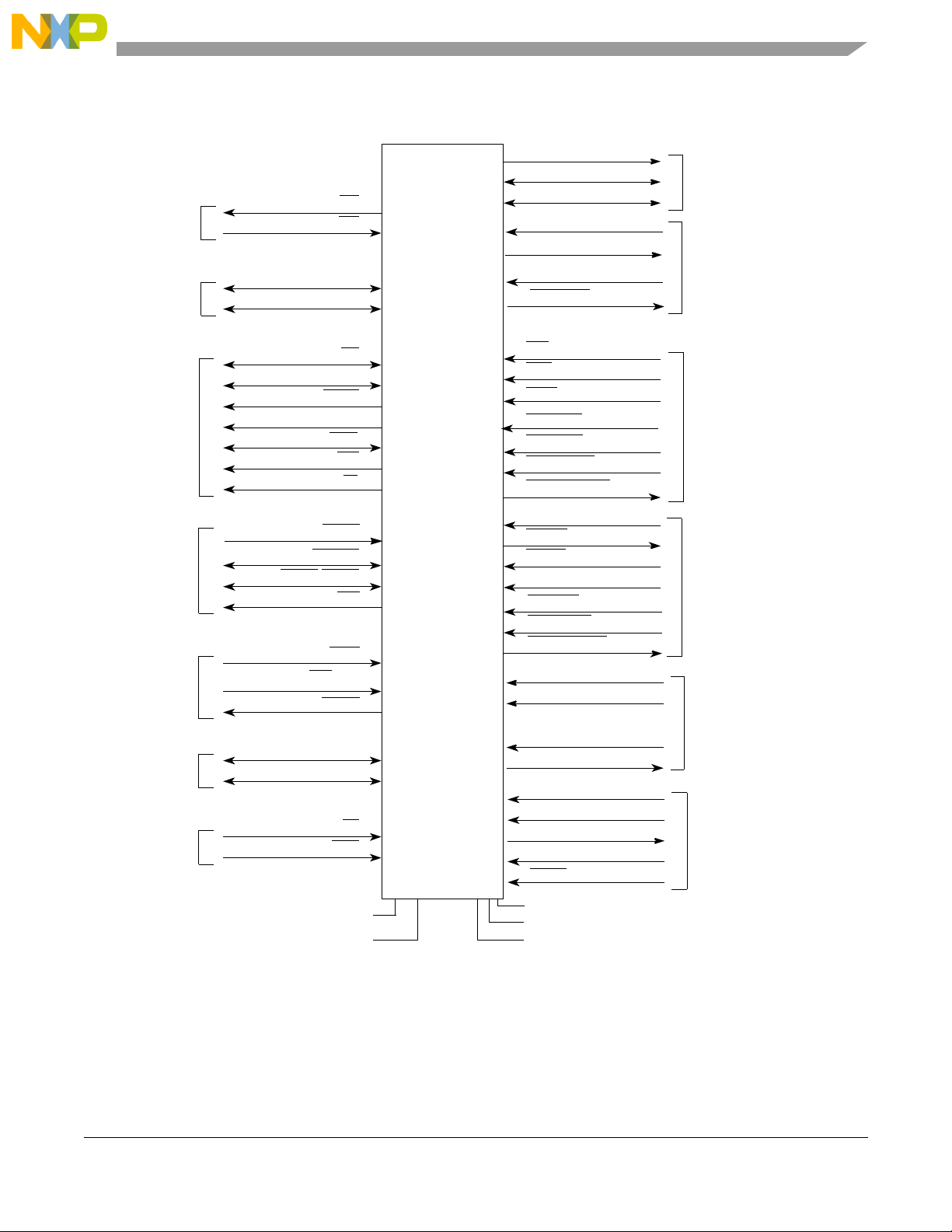
Overview
Figure 1-9 illustrates the signal configuration in MPX bus mode for the MPC7447 and the MPC7457.
Address
Arbitration
Address
Tr an s fe r
Address
Tr an s fe r
Attributes
BR
BG
A[0:35]
AP[0:4]
TS
TT[0:4]
TBST
TSIZ[0:2]
GBL
WT
CI
1
1
36
5
1
5
1
3
1
1
1
MPC7447/
AACK
Address
Tr an s fe r
Termination
ARTRY
SHD0/SHD1
HIT
DBG
Data
Arbitration
Data
Tr an s fe r
Data
Tr an s fe r
DTI[0:3]
DRDY
D[0:63]
DP[0:7]
TA
TEA
Termination
V
DD
OV
DD
1
For the MPC7457, there are 19 L3_ADDR signals, (L3_ADDR[0:18]).
MPC7457
1
(MPX)
1
2
1
1
4
1
64
8
1
1
18
64
L3_ADDR[17:0]
L3_DATA[0:63]
L3_DP[0:7]
8
L3_VSEL
1
L3_CLK[0:1]
2
L3_ECHO_CLK[0:3]
4
L3_CNTL
2
INT
1
SMI
1
MCP
1
SRESET
1
HRESET
1
CKSTP_IN
1
CKSTP_OUT
1
TBEN
1
QREQ
1
QACK
1
BVSEL
1
BMODE[0:1]
2
PMON_IN
1
PMON_OUT
1
SYSCLK
1
PLL_CFG[0:4]
5
EXT_QUAL
1
CLK_OUT
1
TCK
1
TDI
1
TDO
1
TMS
1
TRST
1
AV
DD
GV
DD
GND
[0:1]
1
L3 Cache
Address/Data
Note: L3 cache interface is
not supported in the
MPC7447.
L3 Cache
Clock/
Control
Interrupts/
Resets
Processor
Status/
Control
Clock
Control
Te st
Interface
(JTAG)
Figure 1-9. MPX Bus Signal Groups in the MPC7447 and MPC7457
MPC7450 RISC Microprocessor Family Reference Manual, Rev. 5
Freescale Semiconductor 1-29
Page 88
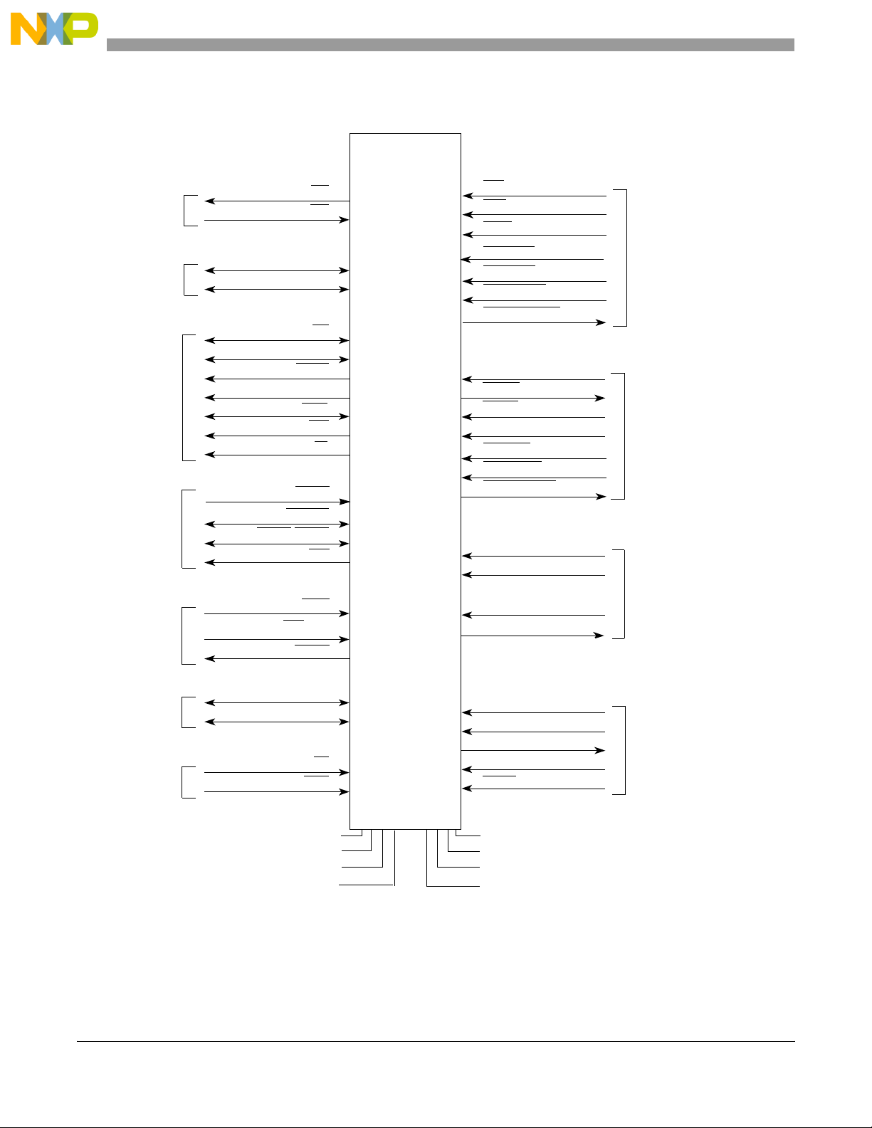
Overview
Figure 1-10 illustrates the signal configuration in MPX bus mode for the MPC7447A.
Address
Arbitration
Address
Tr an s fe r
Address
Tr an s fe r
Attributes
Address
Tr an s fe r
Termination
Data
Arbitration
BR
BG
A[0:35]
AP[0:4]
TS
TT[0:4]
TBST
TSIZ[0:2]
GBL
WT
CI
AACK
ARTRY
SHD0/SHD1
HIT
DBG
DTI[0:3]
DRDY
1
1
36
5
1
5
1
3
1
1
1
MPC7447A
1
(MPX)
1
2
1
1
4
1
INT
1
SMI
1
MCP
1
SRESET
1
HRESET
1
CKSTP_IN
1
CKSTP_OUT
1
TBEN
1
QREQ
1
QACK
1
BVSEL
1
2
1
1
SYSCLK
1
PLL_CFG[0:4]
5
EXT_QUAL
1
CLK_OUT
1
BMODE[0:1]
PMON_IN
PMON_OUT
Interrupts/
Resets
Processor
Status/
Control
Clock
Control
Data
Tr an s fe r
Data
Tr an s fe r
Termination
D[0:63]
DP[0:7]
TA
TEA
V
VDD_SENSE
OV
OVDD_SENSE
DD
DD
64
8
1
1
1
1
1
1
1
TCK
TDI
TDO
TMS
TRST
AV
DD
GV
DD
GND
GND_SENSE
Te st
Interface
(JTAG)
Figure 1-10. MPX Bus Signal Groups in the MPC7447A
MPC7450 RISC Microprocessor Family Reference Manual, Rev. 5
1-30 Freescale Semiconductor
Page 89

Figure 1-11illustrates the signal configuration in MPX bus mode for the MPC7448.
Overview
Address
Arbitration
Address
Tr an s fe r
Address
Tr an s fe r
Attributes
Address
Tr an s fe r
Termination
BR
BG
A[0:35]
AP[0:4]
TS
TT[0:4]
TBST
TSIZ[0:2]
GBL
WT
CI
AACK
ARTRY
SHD0/SHD1
HIT
1
1
36
5
1
5
1
3
1
1
1
MPC7448
1
(MPX)
1
2
1
1
1
1
1
1
1
1
1
1
1
2
1
1
1
1
1
2
INT
SMI
MCP
SRESET
HRESET
CKSTP_IN
CKSTP_OUT
TBEN
QREQ
QACK
BMODE[0:1]
PMON_IN
PMON_OUT
DFS2
DFS4
LV RA M
BVSEL[0:1]
Interrupts/
Reset/
Processor
Status/
Control
Data
Arbitration
Data
Tr an s fe r
Data
Tr an s fe r
Termination
DBG
DTI[0:3]
DRDY
D[0:63]
DP[0:7]
TA
TEA
V
VDD_SENSE
OV
OVDD_SENSE
DD
DD
1
4
1
64
8
1
1
1
4
1
1
1
1
1
1
1
SYSCLK
PLL_CFG[0:5]
EXT_QUAL
CLK_OUT
TCK
TDI
TDO
TMS
TRST
AV
DD
GV
DD
GND
GND_SENSE
Clock
Control
Te st
Interface
(JTAG)
Figure 1-11. MPX Bus Signal Groups in the MPC7448
Signal functionality is described in detail in Chapter 8, “Signal Descriptions,” and Chapter 9, “System
Interface Operation.”
MPC7450 RISC Microprocessor Family Reference Manual, Rev. 5
Freescale Semiconductor 1-31
Page 90

Overview
1.2.9.3.1 Clocking
For functional operation, the MPC7450 uses a single clock input signal, SYSCLK, from which clocking
is derived for the processor core, the L3 interface, and the MPX bus interface. Additionally, internal clock
information is made available at the pins to support debug and development.
The MPC7450’s clocking structure supports a wide range of processor-to-bus clock ratios. The internal
processor core clock is synchronized to SYSCLK with the aid of a VCO-based PLL. The PLL_CFG[0:4]
signals (PLL_CFG[0:5] in the MPC7448) are used to program the internal clock rate to a multiple of
SYSCLK as defined in the hardware specifications. The bus clock is maintained at the same frequency as
SYSCLK. SYSCLK does not need to be a 50% duty-cycle signal.
The MPC7450 generates the clock for the external L3 synchronous data RAMs. The clock frequency for
the RAMs is divided down from (and phase-locked to) the MPC7450 core clock frequency using a divisor
selected through L3CR[L3CLK]. Note that the MPC7441, MPC7445, MPC7447, MPC7447A, and
MPC7448 do not support the L3 cache or the L3 cache interface.
1.2.10 Power and Thermal Management
The MPC7450 is designed for low-power operation. It provides both automatic and program-controlled
power reduction modes. If an MPC7450 functional unit is idle, it automatically goes into a low-power
mode. This mode does not affect operational performance. Dynamic power management automatically
supplies or withholds power to execution units individually, based upon the contents of the instruction
stream. The operation of dynamic power management is transparent to software or any external hardware.
The following three programmable power modes are available to the system:
• Nap—Instruction fetching is halted. Only those clocks for time base, decrementer, and JT AG logic
remain running. The MPC7450 goes into the doze state to snoop memory operations on the bus and
then back to nap using a QREQ/QACK processor-system handshake protocol.
• Sleep—Power consumption is further reduced by disabling bus snooping, leaving only the PLL in
a locked and running state. All internal functional units are disabled.
• Deep sleep—The system can disable the PLL. The system can then disable the SYSCLK source
for greater system power savings. Power-on reset procedures for restarting and relocking the PLL
must be followed upon exiting deep sleep.
The dynamic frequency switching (DFS) feature in the MPC7447A conserves power by lowering
processor operating frequency . The MPC7447A adds the ability to di vide the processor-to-system bus ratio
by two during normal functional operation. With the introduction of DFS4 mode in the MPC7448, the
processor-to-system bus ratio can also be divided by four . Section 10.2.5, “Dynamic Frequency Switching
(DFS),” provide information on power saving with DFS in the MPC7447A and the MPC7448.
The MPC7450 also provides an instruction cache throttling mechanism to effectively reduce the
instruction execution rate without the complexity and overhead of dynamic clock control. When used with
the dynamic power management, instruction cache throttling provides the system designer with a flexible
way to control device temperature while allowing the processor to continue operating. For thermal
management, the MPC7450 provides a supervisor-level instruction cache throttling control register
MPC7450 RISC Microprocessor Family Reference Manual, Rev. 5
1-32 Freescale Semiconductor
Page 91

Overview
(ICTC). Chapter 10, “Power and Thermal Management,” provides information about how to configure the
ICTC register for the MPC7450.
1.2.11 Performance Monitor
The MPC7450 incorporates a performance monitor facility that system designers can use to help bring up,
debug, and optimize software performance. The performance monitor counts events during execution of
instructions related to dispatch, execution, completion, and memory accesses.
The performance monitor incorporates several registers that can be read and written to by supervisor-level
software. User-level versions of these registers provide read-only access for user-level applications. These
registers are described in Section 1.3.1, “PowerPC Registers and Programming Model.” Performance
monitor control registers, MMCR0, MMCR1, and MMCR2 can be used to specify which events are to be
counted and the conditions for which a performance monitoring exception is taken. Additionally, the
sampled instruction address register, SIAR (USIAR), holds the address of the first instruction to complete
after the counter overflowed.
Attempting to write to a user-level read-only performance monitor register causes a program exception,
regardless of the MSR[PR] setting.
When a performance monitor exception occurs, program execution continues from vector offset 0x00F00.
Chapter 11, “Performance Monitor,” describes the operation of the performance monitor diagnostic tool
incorporated in the MPC7450.
1.3 MPC7450 Microprocessor: Architectural Implementation
The PowerPC architecture consists of three layers. Adherence to the PowerPC architecture can be
described in terms of which of the following levels of the architecture is implemented:
• PowerPC user instruction set architecture (UISA)—Defines the base user-level instruction set,
user-level registers, data types, floating-point exception model, memory models for a uniprocessor
environment, and programming model for a uniprocessor environment
• PowerPC virtual environment architecture (VEA)—Describes the memory model for a
multiprocessor environment, defines cache control instructions, and describes other aspects of
virtual environments. Implementations that conform to the VEA also adhere to the UISA but may
not necessarily adhere to the OEA.
• PowerPC operating environment architecture (OEA)—Defines the memory management model,
supervisor-level registers, synchronization requirements, and the exception model.
Implementations that conform to the OEA also adhere to the UISA and the VEA.
The MPC7450 implementation supports the three levels of the architecture described above. For more
information about the PowerPC architecture, see PowerPC Microprocessor Family: the Programming
Environments. Specific MPC7450 features are listed in Section 1.2, “MPC7450 Microprocessor
Features.”
This section describes the PowerPC architecture in general, and specific details about the implementation
of the MPC7450 as a low-power, 32-bit device that implements this architecture. The structure of this
section follows the reference manual organization; each subsection provides an overview of that chapter.
MPC7450 RISC Microprocessor Family Reference Manual, Rev. 5
Freescale Semiconductor 1-33
Page 92

Overview
• Registers and programming model—Section 1.3.1, “PowerPC Registers and Programming
Model,” describes the registers for the operating environment architecture common among
processors of this family and describes the programming model. It also describes the registers that
are unique to the MPC7450.
Instruction set and addressing modes—Section , “Some registers can be accessed both explicitly
and implicitly. In the MPC7450, all SPRs are 32 bits wide. Table 2-1 describes registers
implemented by the MPC7450.,” describes the PowerPC instruction set and addressing modes for
the PowerPC operating environment architecture, and defines and describes the PowerPC
instructions implemented in the MPC7450. The information in this section is described more fully
in Chapter 2, “Programming Model.”
• Cache implementation—Section 1.3.3, “On-Chip Cache Implementation,” describes the cache
model that is defined generally by the virtual environment architecture. It also provides specific
details about the MPC7450 cache implementation. The information in this section is described
more fully in Chapter 3, “L1, L2, and L3 Cache Operation.”
• Exception model—Section 1.3.4, “Exception Model,” describes the exception model of the
PowerPC operating environment architecture and the differences in the MPC7450 exception
model. The information in this section is described more fully in Chapter 4, “Exceptions.”
• Memory management—Section 1.3.5, “Memory Management,” describes generally the
conventions for memory management. This section also describes the MPC7450’s implementation
of the 32-bit PowerPC memory management specification. The information in this section is
described more fully in Chapter 5, “Memory Management.”
• Instruction timing—Section 1.3.6, “Instruction Timing,” provides a general description of the
instruction timing provided by the superscalar, parallel execution supported by the PowerPC
architecture and the MPC7450. The information in this section is described more fully in
Chapter 6, “Instruction Timing.”
• AltiVec implementation—Section 1.3.7, “AltiVec Implementation,” points out that the MPC7450
implements AltiVec registers, instructions, and exceptions as described in the AltiVec Technology
Programming Envir onments Manual. Chapter 7, “AltiVec Technology Implementation,” provides
complete details.
1.3.1 PowerPC Registers and Programming Model
The PowerPC architecture defines register-to-register operations for most computational instructions.
Source operands for these instructions are accessed from the registers or are provided as immediate values
embedded in the instruction opcode. The three-register instruction format allows specification of a target
register distinct from the two source operands. Load and store instructions trans fer data between registers
and memory.
The PowerPC architecture also defines two levels of privilege—supervisor mode of operation (typically
used by the operating system) and user mode of operation (used by the application software). The
programming models incorporate 32 GPRs, 32 FPRs, SPRs, and several miscellaneous registers. The
AltiVec extensions to the PowerPC architecture augment the programming model with 32 VRs, 1 status
and control register, and 1 save and restore register. Each processor that implements the PowerPC
MPC7450 RISC Microprocessor Family Reference Manual, Rev. 5
1-34 Freescale Semiconductor
Page 93

Overview
architecture also has a unique set of implementation-specific registers to support functionality that may not
be defined by the PowerPC architecture.
Having access to privileged instructions, registers, and other resources allows the operating system to
control the application environment (providing virtual memory and protecting operating-system and
critical machine resources). Instructions that control the state of the processor, the address translation
mechanism, and supervisor registers can be executed only when the processor is operating in supervisor
mode.
Figure 1-12 through Figure 1-13 show all the MPC7450 registers available at the user and supervisor level.
The numbers to the right of the SPRs indicate the number that is used in the syntax of the instruction
operands to access the register. For more information, see Chapter 2, “Programming Model.”
The OEA defines numerous SPRs that serve a variety of functions, such as providing controls, indicating
status, configuring the processor, and performing special operati ons. During normal execution, a program
can access the registers shown in Figure 1-12 through Figure 1-13, depending on the program’s access
privilege (supervisor or user, determined by the privilege-level bit, MSR[PR]). GPRs, FPRs, and VRs are
accessed through operands that are part of the instructions. Access to registers can be explicit (that is,
through the use of specific instructions for that purpose such as Move to Special-Purpose Register (mtspr)
and Move from Special-Purpose Register (mfspr) instructions) or implicit, as the part of the execution of
an instruction.
MPC7450 RISC Microprocessor Family Reference Manual, Rev. 5
Freescale Semiconductor 1-35
Page 94

Overview
Figure 1-12 shows the MPC7441 and MPC7451 register set.
USER MODEL – VEA
Time Base Facility (For Reading)
TBL
TBR 268 TBR 269
TBU
USER MODEL – UISA
Count Register
CTR
XER
XER
Link Register
LR
SPR 9
SPR 1
SPR 8
General-Purpose
Performance Monitor Registers
Performance Counters
UPMC1
UPMC2
UPMC3
UPMC4
UPMC5
UPMC6
Sampled Instruction
Address
USIAR
SPR 937
SPR 938
SPR 941
SPR 942
SPR 929
SPR 930
1
SPR 939
Monitor Control
UMMCR0
UMMCR1
UMMCR2
SPR 936
SPR 940
SPR 928
1
Condition Register
1
Control Register
AltiVec Registers
Vector Save/Restore
Register
Vector Status and
Control Register
3
VRSAVE
SPR 256
3
VSCR
Vector Registers
Miscellaneous Registers
Time Base
(For Writing)
TBL
TBU
Instruction Address
Breakpoint Register
IABR
SPR 284
SPR 285
SPR 1010
Data Address
Breakpoint Register
DABR
External Access
Register
1
EAR SPR 282
Decrementer
DEC
Registers
GPR0
GPR1
GPR31
Floating-Point
Registers
FPR0
FPR1
FPR31
CR
Floating-Point
Status and
FPSCR
VR0
VR1
VR31
SPR 1013
2
SPR 22
SUPERVISOR MODEL – OEA
Hardware
Implementation
Registers
HID0
HID1
Configuration Registers
1
SPR 1008
SPR 1009
Memory Management Registers
Instruction BAT
Registers
IBAT0U
IBAT0L
IBAT1U
IBAT1L
IBAT2U
IBAT2L
IBAT3U
IBAT3L
SPR 528
SPR 529
SPR 530
SPR 531
SPR 532
SPR 533
SPR 534
SPR 535
SDR1
SDR1
SPR 25
Exception Handling Registers
SPRGs
SPRG0
SPRG1
SPRG2
SPRG3
SPR 272
SPR 273
SPR 274
SPR 275
Cache/Memory Subsystem Registers
Load/Store
Control Register
3
LDSTCR SPR 1016
Memory Subsystem
Status Control
Registers
MSSCR0
MSSSR0 SPR 1015
1
1
SPR 1014
Performance Monitor Registers
2
Performance
Counters
PMC1
PMC2
PMC3
PMC4
PMC5
PMC6
2
SPR 953
SPR 954
SPR 957
SPR 958
SPR 945
SPR 946
Machine State Register
Processor Version
Register
PVR
Data BAT
Registers
DBAT0U
DBAT0L
DBAT1U
DBAT1L
DBAT2U
DBAT2L
DBAT3U
DBAT3L
SPR 287
SPR 536
SPR 537
SPR 538
SPR 539
SPR 540
SPR 541
SPR 542
SPR 543
MSR
Processor ID Register
PIR
Segment Registers
SR0
SR1
SR15
PTE High/Low
Registers
PTEHI
PTELO
TLB Miss Register
TLBMISS SPR 980
Data Address
Register
DAR
SPR 19
DSISR
DSISR
Instruction Cache/
Interrupt Control
Register
ICTRL
L2 Cache Control
Register
L2CR
SPR 18
1
SPR 1011
1
SPR 1017
Save and Restore
Registers
SRR0
SRR1
1
L3 Private Memory
4
Register
L3PM
L3 Cache Control
4
Register
L3CR SPR 1018
L3 Cache Input Timing
Control Register
L3ITCR0 SPR 984
Monitor Control
Registers
MMCR0
MMCR1
MMCR2
2
2
1
SPR 952
SPR 956
SPR 944
Breakpoint Address
Mask Register
BAMR
Sampled Instruction
Address Register
SIAR
Thermal Management Register
Instruction Cache Throttling
Control Register
ICTC
1
SPR 1019
2
SPR 1023
1
SPR 981
SPR 982
1
SPR 26
SPR 27
SPR 983
4
1
SPR 951
2
SPR 955
1
MPC7441-, MPC7451-specific register may not be supported on other processors that implement the PowerPC architecture.
2
Register defined as optional in the PowerPC architecture.
3
Register defined by the AltiVec technology.
4
MPC7451-specific register.
Figure 1-12. Programming Model—MPC7441/MPC7451 Microprocessor Registers
MPC7450 RISC Microprocessor Family Reference Manual, Rev. 5
1-36 Freescale Semiconductor
Page 95

Figure 1-13 shows the MPC7445, MPC7455, MPC7447, MPC7457, and MPC7447A register set.
Overview
USER MODEL – VEA
Time Base Facility (For Reading)
TBL
TBR 268 TBR 269
TBU
USER MODEL – UISA
Count Register
CTR
XER
XER
Link Register
LR
SPR 9
SPR 1
SPR 8
General-Purpose
Registers
GPR0
GPR1
GPR31
Performance Monitor Registers
Performance Counters
UPMC1
UPMC2
UPMC3
UPMC4
UPMC5
UPMC6
Sampled Instruction
Address
USIAR
Monitor Control
UMMCR0
UMMCR1
UMMCR2
SPR 937
SPR 938
SPR 941
SPR 942
SPR 929
SPR 930
1
SPR 939
1
SPR 936
SPR 940
SPR 928
1
Condition Register
Registers
FPR0
FPR1
FPR31
CR
Floating-Point
Status and
Control Register
FPSCR
Floating-Point
AltiVec Registers
Vector Save/Restore
3
Register
VRSAVE
Vector Status and
Control Register
SPR 256
3
VSCR
Vector Registers
VR0
VR1
VR31
Miscellaneous Registers
Time Base
(For Writing)
TBL
TBU
Instruction Address
Breakpoint Register
IABR
SPR 284
SPR 285
SPR 1010
Data Address
Breakpoint Register
DABR
External Access
2
Register
1
EAR SPR 282
Decrementer
DEC
SPR 1013
SPR 22
Thermal Management Register
Instruction Cache Throttling
Control Register
ICTC
1
MPC7445-, MPC7447-, MPC7455-, and MPC7457-specific register may not be supported on other processors that implement
the PowerPC architecture.
2
Register defined as optional in the PowerPC architecture.
3
Register defined by the AltiVec technology.
4
MPC7455- and MPC7457-specific register.
5
MPC7457-specific register.
1
SPR 1019
Hardware
Implementation
Registers
HID0
HID1
Instruction BAT
Registers
IBAT0U
IBAT0L
IBAT1U
IBAT1L
IBAT2U
IBAT2L
IBAT3U
IBAT3L
IBAT4U
IBAT4L
IBAT5U
IBAT5L
IBAT6U
IBAT6L
IBAT7U
IBAT7L
SPRGs
SPRG0
SPRG1
SPRG2
SPRG3
3
SPRG4
SPRG5
SPRG6
SPRG7
Load/Store
Control Register
LDSTCR SPR 1016
Memory Subsystem
Status Control
Registers
2
MSSCR0
MSSSR0 SPR 1015
Performance
Counters
PMC1
PMC2
PMC3
PMC4
PMC5
PMC6
Configuration Registers
1
SPR 1008
SPR 1009
Processor Version
Register
PVR
SPR 287
Memory Management Registers
Data BAT
Registers
1
1
1
1
1
1
1
1
SPR 528
SPR 529
SPR 530
SPR 531
SPR 532
SPR 533
SPR 534
SPR 535
SPR 560
SPR 561
SPR 562
SPR 563
SPR 564
SPR 565
SPR 566
SPR 567
DBAT0U
DBAT0L
DBAT1U
DBAT1L
DBAT2U
DBAT2L
DBAT3U
DBAT3L
DBAT4U
DBAT4L
DBAT5U
DBAT5L
DBAT6U
DBAT6L
DBAT7U
DBAT7L
1
1
1
1
1
1
1
1
SPR 536
SPR 537
SPR 538
SPR 539
SPR 540
SPR 541
SPR 542
SPR 543
SPR 568
SPR 569
SPR 570
SPR 571
SPR 572
SPR 573
SPR 574
SPR 575
Exception Handling Registers
Data Address
SPR 272
SPR 273
Register
DAR
SPR 19
SPR 274
1
1
1
1
SPR 275
SPR 276
SPR 277
SPR 278
SPR 279
DSISR
DSISR
SPR 18
Cache/Memory Subsystem Registers
1
2
1
Instruction Cache/
Interrupt Control
Register
ICTRL
L2 Cache Control
Register
SPR 1014
L2CR
L3 Cache Output Hold
ControlRegister
L3OHCR SPR 1000
Performance Monitor
Registers
SPR 953
SPR 954
SPR 957
SPR 958
SPR 945
SPR 946
Monitor Control
Registers
MMCR0
MMCR1
MMCR2
1
1
SPR 1011
SPR 1017
2
SPR 952
2
SPR 956
1
SPR 944
5
Machine State Register
MSR
Processor ID Register
PIR
SPR 1023
Segment Registers
SR0
SR1
SR15
PTE High/Low
Registers
TLB Miss Register
PTEHI
PTELO
1
SPR 981
SPR 982
1
TLBMISS SPR 980
SDR1
SDR1
Save and Restore
Registers
SRR0
SRR1
1
L3 Private Memory
Register
L3PM
L3 Cache Control
Register
L3CR
L3 Cache Input Timing
Control Register
SPR 25
SPR 26
SPR 27
4
SPR 983
4
SPR 1018
L3ITCR0 SPR 984
Breakpoint Address
Mask Register
BAMR
Sampled Instruction
Address Register
SIAR
1
SPR 951
2
SPR 955
2
Figure 1-13. Programming Model—MPC7445, MPC7447, MPC7455, MPC7457, and MPC7447A
Microprocessor Registers
SUPERVISOR MODEL – OEA
MPC7450 RISC Microprocessor Family Reference Manual, Rev. 5
Freescale Semiconductor 1-37
Page 96

Overview
Figure 1-14 shows the MPC7448 register set.
USER MODEL – VEA
Time Base Facility (For Reading)
TBL
TBR 268 TBR 269
TBU
USER MODEL – UISA
Count Register
CTR
XER
XER
Link Register
LR
SPR 9
SPR 1
SPR 8
General-Purpose
Registers
GPR0
GPR1
GPR31
Performance Monitor Registers
Performance Counters
UPMC1
UPMC2
UPMC3
UPMC4
UPMC5
UPMC6
Sampled Instruction
Address
USIAR
Monitor Control
UMMCR0
UMMCR1
UMMCR2
SPR 937
SPR 938
SPR 941
SPR 942
SPR 929
SPR 930
1
SPR 939
1
SPR 936
SPR 940
SPR 928
1
Condition Register
Registers
FPR0
FPR1
FPR31
CR
Floating-Point
Status and
Control Register
FPSCR
Floating-Point
AltiVec Registers
Vector Save/Restore
Register
Vector Status and
Control Register
VRSAVE
3
SPR 256
3
VSCR
Vector Registers
VR0
VR1
VR31
Miscellaneous Registers
Time Base
(For Writing)
TBL
TBU
Instruction Address
Breakpoint Register
IABR
SPR 284
SPR 285
SPR 1010
Data Address
Breakpoint Register
DABR
External Access
Register
1
EAR SPR 282
Decrementer
DEC
SPR 1013
2
SPR 22
Thermal Management Register
Instruction Cache Throttling
Control Register
ICTC
1
MPC7448-specific register may not be supported on other processors that implement the PowerPC architecture.
2
Register defined as optional in the PowerPC architecture.
3
Register defined by the AltiVec technology.
1
SPR 1019
Hardware
Implementation
Registers
HID0
HID1
Instruction BAT
Registers
IBAT0U
IBAT0L
IBAT1U
IBAT1L
IBAT2U
IBAT2L
IBAT3U
IBAT3L
IBAT4U
IBAT4L
IBAT5U
IBAT5L
IBAT6U
IBAT6L
IBAT7U
IBAT7L
SPRGs
SPRG0
SPRG1
SPRG2
SPRG3
3
SPRG4
SPRG5
SPRG6
SPRG7
Load/Store
Control Register
LDSTCR SPR 1016
Memory Subsystem
Status Control
Registers
2
MSSCR0
MSSSR0 SPR 1015
Performance
Counters
PMC1
PMC2
PMC3
PMC4
PMC5
PMC6
Configuration Registers
1
SPR 1008
SPR 1009
Processor Version
Register
PVR
SPR 287
Memory Management Registers
Data BAT
Registers
1
1
1
1
1
1
1
1
SPR 528
SPR 529
SPR 530
SPR 531
SPR 532
SPR 533
SPR 534
SPR 535
SPR 560
SPR 561
SPR 562
SPR 563
SPR 564
SPR 565
SPR 566
SPR 567
DBAT0U
DBAT0L
DBAT1U
DBAT1L
DBAT2U
DBAT2L
DBAT3U
DBAT3L
DBAT4U
DBAT4L
DBAT5U
DBAT5L
DBAT6U
DBAT6L
DBAT7U
DBAT7L
1
1
1
1
1
1
1
1
SPR 536
SPR 537
SPR 538
SPR 539
SPR 540
SPR 541
SPR 542
SPR 543
SPR 568
SPR 569
SPR 570
SPR 571
SPR 572
SPR 573
SPR 574
SPR 575
Exception Handling Registers
Data Address
Register
DAR
SPR 19
DSISR
DSISR
SPR 18
Cache/Memory Subsystem Registers
Instruction Cache/
Interrupt Control
Register
L2 Cache Control
Register
L2 Error Injection
Registers
ICTRL
L2CR
1
SPR 1011
1
SPR 1017
1
1
1
1
1
1
SPR 272
SPR 273
SPR 274
SPR 275
SPR 276
SPR 277
SPR 278
SPR 279
1
SPR 1014
L2ERRINJHI1SPR 985
L2ERRINJLO1SPR 986
L2ERRINJCTL1SPR 987
Performance Monitor Registers
2
SPR 953
SPR 954
SPR 957
SPR 958
SPR 945
SPR 946
Monitor Control
Registers
MMCR0
MMCR1
MMCR2
2
2
1
SPR 952
SPR 956
SPR 944
Figure 1-14. Programming Model—MPC7448 Microprocessor Registers
SUPERVISOR MODEL – OEA
Machine State Register
MSR
Processor ID Register
PIR
SPR 1023
Segment Registers
SR0
SR1
SR15
PTE High/Low
Registers
PTEHI
PTELO
1
SPR 981
SPR 982
TLB Miss Register
TLBMISS SPR 980
SDR1
SDR1
Save and Restore
Registers
SRR0
SRR1
L2 Error Control and
Capture Registers
L2CAPTDATAHI
L2CAPTDATALO
L2CAPTECC
L2ERRDET
L2ERRDIS
L2ERRINTEN
L2ERRATTR
L2ERRADDR
L2ERREADDR
L2ERRCTL
Breakpoint Address
Mask Register
BAMR
Sampled Instruction
Address Register
SIAR
SPR 25
SPR 26
SPR 27
1
1
1
1
1
1
1
1
1
1
1
SPR 951
SPR 955
1
SPR 988
SPR 989
SPR 990
SPR 991
SPR 992
SPR 993
SPR 994
SPR 995
SPR 996
SPR 997
2
2
1
1
MPC7450 RISC Microprocessor Family Reference Manual, Rev. 5
1-38 Freescale Semiconductor
Page 97

Overview
Some registers can be accessed both explicitly and implicitly . In the MPC7450, all SPRs are 32 bits wide.
Table 2-1 describes registers implemented by the MPC7450.
1.3.2 Instruction Set
All PowerPC instructions are encoded as single-word (32-bit) opcodes. Instruction formats are consistent
among all instruction types, permitting efficient decoding to occur in parallel with operand accesses. This
fixed instruction length and consistent format greatly simplifies instruction pipelining.
For more information, see Chapter 2, “Programming Model.”
1.3.2.1 PowerPC Instruction Set
The PowerPC instructions are divided into the following categories:
• Integer instructions—These include computational and logical instructions.
— Integer arithmetic instructions
— Integer compare instructions
— Integer logical instructions
— Integer rotate and shift instructions
• Floating-point instructions—These include floating-point computational instructions, as well as
instructions that affect the FPSCR.
— Floating-point arithmetic instructions
— Floating-point multiply/add instructions
— Floating-point rounding and conversion instructions
— Floating-point compare instructions
— Floating-point status and control instructions
• Load and store instructions—These include integer and floating-point load and store instructions.
— Integer load and store instructions
— Integer load and store multiple instructions
— Floating-point load and store instructions
— Primitives used to construct atomic memory operations (lwarx and stwcx. instructions)
• Flow control instructions—These include branching instructions, condition register logical
instructions, trap instructions, and other instructions that affect the instruction flow.
— Branch and trap instructions
— Condition register logical instructions
MPC7450 RISC Microprocessor Family Reference Manual, Rev. 5
Freescale Semiconductor 1-39
Page 98

Overview
• Processor control instructions—These instructions are used for synchronizing memory accesses
and management of caches, TLBs, and the segment registers.
— Move to/from SPR instructions
— Move to/from MSR
— Synchronize
— Instruction synchronize
— Order loads and stores
• Memory control instructions—These instructions provide control of caches, TLBs, and SRs.
— Supervisor-level cache management instructions
— User-level cache instructions
— Segment register manipulation instructions
— Translation lookaside buffer management instructions
This grouping does not indicate the execution unit that executes a particular instruction or group of
instructions.
Integer instructions operate on byte, half-word, and word operands. Floating-point instructions operate on
single-precision (one word) and double-precision (one double word) floating-point operands. The
PowerPC architecture uses instructions that are four bytes long and word-aligned. It provides for byte,
half-word, and word operand loads and stores between memory and a set of 32 GPRs. It also provides for
word and double-word operand loads and stores between memory and a set of 32 floating-point registers
(FPRs).
Computational instructions do not modify memory. To use a memory operand in a computation and then
modify the same or another memory location, the memory contents must be loaded into a register,
modified, and then written back to the target location with distinct instructions.
Processors that implement the PowerPC architecture follow the program flow when they are in the normal
execution state. However, the flow of instructions can be interrupted directly by the execution of an
instruction or by an asynchronous event. Either kind of exception may cause one of several components
of the system software to be invoked.
Effective address computations for both data and instruction accesses use 32-bit unsigned binary
arithmetic. A carry from bit 0 is ignored in 32-bit implementations.
1.3.2.2 AltiVec Instruction Set
The AltiVec instructions are divided into the following categories:
• Vector integer arithmetic instructions—These include arithmetic, logical, compare, rotate, and
shift instructions.
• V ector floating-point arithmetic instructions—These include floating-poin t arithmetic instructions,
as well as a discussion on floating-point modes.
MPC7450 RISC Microprocessor Family Reference Manual, Rev. 5
1-40 Freescale Semiconductor
Page 99

Overview
• Vector load and store instructions—These include load and store instructions for vector registers.
The AltiVec technology defines LRU and transient type instructions that can be used to optimize
memory accesses.
— LRU instructions. The AltiVec architecture specifies that the lvxl and stvxl instructions differ
from other AltiVec load and store instructions in that they leave cache entries in a
least-recently-used (LRU) state instead of a most-recently-used state.
— Transient instructions. The AltiVec architecture describes a difference between static and
transient memory accesses. A static memory access should have some reasonable degree of
locality and be referenced several times or reused over some reasonably long period of time. A
transient memory reference has poor locality and is likely to be referenced a very few times or
over a very short period of time.
The following instructions are interpreted to be transient:
– dstt and dststt (transient forms of the two data stream touch instructions)
– lvxl and stvxl
• Vector permutation and formatting instructions—These include pack, unpack, merge, splat,
permute, select, and shift instructions, described in Section 2.6.5, “Vector Permutation and
Formatting Instructions.”
• Processor control instructions—These instructions are used to read and write from the AltiVec
status and control register, described in Section 2.4.4.6, “Processor Control Instructions.”
• Memory control instructions—These instructions are used for managing of caches (user level and
supervisor level), described in Section 2.4.5.3, “Memory Control Instructions.”
1.3.2.3 MPC7450 Microprocessor Instruction Set
The MPC7450 instruction set is defined as follows:
• The MPC7450 provides hardware support for all 32-bit PowerPC instructions.
• The MPC7450 implements the following instructions optional to the PowerPC architecture:
— External Control In Word Indexed (eciwx)
— External Control Out Word Indexed (ecowx)
— Data Cache Block Allocate (dcba)
— Floating Select (fsel)
— Floating Reciprocal Estimate Single-Precision (fres)
— Floating Reciprocal Square Root Estimate (frsqrte)
— Store Floating-Point as Integer Word (stfiwx)
— Load Data TLB Entry (tlbld)
— Load Instruction TLB Entry (tlbli)
MPC7450 RISC Microprocessor Family Reference Manual, Rev. 5
Freescale Semiconductor 1-41
Page 100

Overview
1.3.3 On-Chip Cache Implementation
The following subsections describe the PowerPC architecture’s treatment of cache in general, and the
MPC7450-specific implementation, respectively. A detailed description of the MPC7450 cache
implementation is provided in Chapter 3, “L1, L2, and L3 Cache Operation.”
1.3.3.1 PowerPC Cache Model
The PowerPC architecture does not define hardware aspects of cache implementations. For example,
processors that implement the PowerPC architecture can have unified caches, separate L1 instruction and
data caches (Harvard architecture), or no cache at all. These microprocessors control the following
memory access modes on a page or block basis:
• Write-back/write-through mode
• Caching-inhibited/caching-allowed mode
• Memory coherency required/memory coherency not required mode
The caches are physically addressed, and the data cache can operate in either write-back or write-through
mode as specified by the PowerPC architecture.
The PowerPC architecture defines the term ‘cache block’ as the cacheable unit. The VEA and OEA define
cache management instructions a programmer can use to affect cache contents.
1.3.3.2 MPC7450 Microprocessor Cache Implementation
The MPC7450 cache implementation is described in Section 1.2.4, “On-Chip L1 Instruction and Data
Caches,” Section 1.2.5, “L2 Cache Implementation,” and Section 1.2.6, “L3 Cache Implementation.” The
BPU also contains a 128-entry BTIC that provides immediate access to cached target instructions. For
more information, see Section 1.2.2.2, “Branch Processing Unit (BPU).”
1.3.4 Exception Model
The following sections describe the PowerPC exception model and the MPC7450 implementation. A
detailed description of the MPC7450 exception model is provided in Chapter 4, “Exceptions.”
1.3.4.1 PowerPC Exception Model
The OEA portion of the PowerPC architecture defines the mech anism by which processors that implement
the PowerPC architecture invoke exceptions. Exception conditions may be defined at other levels of the
architecture. For example, the UISA defines conditions that may cause floating-point exceptions; the OEA
defines the mechanism by which the exception is taken.
The PowerPC exception mechanism allows the processor to change to supervisor state as a result of
unusual conditions arising in the execution of instructions and from external signals, bus errors, or various
internal conditions. When exceptions occur, information about the state of the processor is saved to certain
registers and the processor begins execution at an address (exception vector) predetermined for each
exception. Processing of exceptions begins in supervisor mode.
MPC7450 RISC Microprocessor Family Reference Manual, Rev. 5
1-42 Freescale Semiconductor
 Loading...