

Page 1

MPC184 Security Co-Processor
User’s Manual
PCI Interface
Preliminary—Subject to Change Without Notice
MPC184UM
Rev. 2, 12/2005
Page 2

How to Reach Us:
Home Page:
www.freescale.com
email:
support@freescale.com
USA/Europe or Locations Not Listed:
Freescale Semiconductor
Technical Information Center, CH370
1300 N. Alma School Road
Chandler, Arizona 85224
(800) 521-6274
480-768-2130
support@freescale.com
Europe, Middle East, and Africa:
Freescale Halbleiter Deutschland GmbH
Technical Information Center
Schatzbogen 7
81829 Muenchen, Germany
+44 1296 380 456 (English)
+46 8 52200080 (English)
+49 89 92103 559 (German)
+33 1 69 35 48 48 (French)
support@freescale.com
Japan:
Freescale Semiconductor Japan Ltd.
Headquarters
ARCO Tower 15F
1-8-1, Shimo-Meguro, Meguro-ku
Tokyo 153-0064, Japan
0120 191014
+81 3 5437 9125
support.japan@freescale.com
Asia/Pacific:
Freescale Semiconductor Hong Kong Ltd.
Technical Information Center
2 Dai King Street
Tai Po Industrial Estate,
Tai Po, N.T., Hong Kong
+800 2666 8080
support.asia@freescale.com
For Literature Requests Only:
Freescale Semiconductor
Literature Distribution Center
P.O. Box 5405
Denver, Colorado 80217
(800) 441-2447
303-675-2140
Fax: 303-675-2150
LDCForFreescaleSemiconductor
@hibbertgroup.com
Information in this document is provided solely to enable system and software
implementers to use Freescale Semiconductor products. There are no express or
implied copyright licenses granted hereunder to design or fabricate any integrated
circuits or integrated circuits based on the information in this document.
Freescale Semiconductor reserves the right to make changes without further notice to
any products herein. Freescale Semiconductor makes no warranty, representation or
guarantee regarding the suitability of its products for any particular purpose, nor does
Freescale Semiconductor assume any liability arising out of the application or use of
any product or circuit, and specifically disclaims any and all liability, including without
limitation consequential or incidental damages. “Typical” parameters which may be
provided in Freescale Semiconductor data sheets and/or specifications can and do
vary in different applications and actual performance may vary over time. All operating
parameters, including “Typicals” must be validated for each customer application by
customer’s technical experts. Freescale Semiconductor does not convey any license
under its patent rights nor the rights of others. Freescale Semiconductor products are
not designed, intended, or authorized for use as components in systems intended for
surgical implant into the body, or other applications intended to support or sustain life,
or for any other application in whi ch the failure of the Freescale Semiconductor produc t
could create a situation where personal injury or death may occur. Should Buyer
purchase or use Freescale Semiconductor products for any such unintended or
unauthorized application, Buyer shall indemnify and hold Freescale Semiconductor
and its officers, employees, subsidiaries, affiliates, and distributors har mless against all
claims, costs, damages, and expenses, and reasonable attor ney fees arising out of,
directly or indirectly, any claim of personal injury or death associated with such
unintended or unauthorized use, even if such claim alleges that Freescale
Semiconductor was negligent regarding the d esign or manufacture of the part.
Freescale™ and the Freescale logo are trademarks of Freescale Semiconductor, Inc. All other
product or service names are the property of their respective owners.
© Freescale Semiconductor, Inc., 2005. All rights reserved.
Document Number: MPC184UM
Rev. 2, 12/2005
Preliminary—Subject to Change Without Notice
Page 3

Overview
1
Signal Descriptions
Address Map
PCI Configuration Registers
Execution Units
MPC184 Descriptors
Crypto-Channels
Controller
PCI Interface Module
2
3
4
5
6
7
8
9
Execution Units in 32-Bit Big Endian View
Controller in 32-Bit Big Endian View
User’s Manual Revision History
Preliminary—Subject to Change Without Notice
Index
A
B
C
IND
Page 4

1
Overview
2
3
4
5
6
7
8
9
Signal Descriptions
Address Map
PCI Configuration Registers
Execution Units
MPC184 Descriptors
Crypto-Channels
Controller
PCI Interface Module
A
Execution Units in 32-Bit Big Endian View
B Controller in 32-Bit Big Endian View
C
IND
User’s Manual Revision History
Index
Preliminary—Subject to Change Without Notice
Page 5

Contents
Paragraph
Number Title
Page
Number
Chapter 1
Overview
1.1 Develop m e n t H i st o ry...... ................................................................................................. 1 - 1
1.2 T ypical Applications ........................................................................................................ 1-1
1.3 Features............................................................................................................................ 1-1
1.4 T ypical System Architecture............................................................................................ 1-3
1.5 Archi te c t u ral Overv i e w.... . . . . . . . . . . . . . . . . . . . . . . . . . . . . . . . . . ....... ........................................................ 1-4
1.6 Data Pac k et Descrip tors................................................................................................... 1-5
1.6.1 Externa l Bu s In t erface ................................................................................................. 1-6
1.6.2 The MPC1 84 Co n t roller ..... ....................................... .................................................. 1-7
1.6.3 Host-Managed Register Access................................................................................... 1-7
1.6.4 Static EU Access.......................................................................................................... 1-7
1.6.5 Dynamic EU Access.................................................................................................... 1-7
1.6.6 Crypto-Channels.......................................................................................................... 1-8
1.7 Execut io n Un its (EUs) .... .................. ............................................................................... 1 - 8
1.7.1 Public Key Ex ecution U n i t (PKEU) ............................................................................ 1-9
1.7.1.1 Elliptic Curve Operations........................... ........ .......... .......... .......... .......... .......... ...1-9
1.7.1.2 Modular Exponentiation Operations...................................................................... 1-10
1.7.2 Data Encryptio n Stand a rd Execut i o n U n i t ( D EU )..... ................................................ 1- 1 0
1.7.3 Arc Four Execution Unit (AFEU) ............................................................................. 1-10
1.7.4 Advance d En crypti o n Stand ard Execution Un i t (AESU).......................................... 1-11
1.7.5 M essage Digest Execution Unit (MDEU) Module.................................................... 1-11
1.7.6 Random Number Generator (RNG)........................... .......... ............ .......... ............ .... 1-11
1.7.7 8KB General Purpo s e RA M (gpRAM ) .. ....................................... ............................ 1- 1 2
1.8 Perfor m a n ce Estimates ....... ........................................................................................... 1 - 1 2
1.9 User’s Manual Revis i o n History... ............................................................... .................. 1 -12
Chapter 2
Signal Descriptions
2.1 Signal Descriptions ..........................................................................................................2-1
2.2 MPC184 Pin Out. .............................................................................................................2-4
Chapter 3
Address Map
3.1 Address Map .................................................................................................................... 3-1
MPC184 Security Co-Processor User’s Manual: PCI Interface, Rev. 2
Freescale Semiconductor v
Preliminary—Subject to Change Without Notice
Page 6

Contents
Paragraph
Number Title
Page
Number
Chapter 4
PCI Configuration Registers
4.1 PCI Configuration Space ................................................................................................. 4-1
4.1.1 PCI Vendor ID Register (offset 0x0000) ..................................................................... 4-2
4.1.2 PCI Device ID Register (offset 0x0002)...................................................................... 4-2
4.1.3 PCI Command Register (offset 0x0004) ..................................................................... 4-2
4.1.4 PCI Status Register (offset 0x0006) ............................................................................ 4-3
4.1.5 R evision ID Register (offset 0x0008).......................................................................... 4-4
4.1.6 Class Code Register (offset 0x0009)........................................................................... 4-4
4.1.7 Cache Line Size Register (offset 0x000C) .......................... ............ .......... ............ ...... 4- 4
4.1.8 L atency T imer Register (offset 0x000D).....................................................................4-5
4.1.9 Header -Type Register (offset 0x000E) ........................................................................4-5
4.1.10 BIST Register (offset 0x000F) ....................................................................................4-5
4.1.11 Base Address Register Zero (offset 0x0010)............................................................... 4- 5
4.1.12 Base Address Register 1 (offset 0x0014) ....................................................................4-6
4.1.13 Base Address Register 2 (offset 0x0018) ....................................................................4-6
4.1.14 Base Address Register 3 (offset 0x001C).................................................................... 4-6
4.1.15 Base Address Register 4 (offset 0x0020) ....................................................................4-6
4.1.16 Base Address Register 5 (offset 0x0024) ....................................................................4-7
4.1.17 CardBus CIS Pointer Register (offset 0x0028)............................................................ 4-7
4.1.18 Subsystem Vendor ID Register (offset 0x002C).......................................................... 4-7
4.1.19 Subsystem ID Register (offset 0x002E) ......................................................................4-7
4.1.20 Expansion ROM Base Address Register (offset 0x0030) ........................................... 4-8
4.1.21 Capabilities Pointer (offset 0x0034)............................................................................4-8
4.1.22 Interrupt Line Register (offset 0x003C) ...................................................................... 4-8
4.1.23 Interrupt Pin Register (offset 0x003D)........................................................................4-8
4.1.24 Min_GNT Register (offset 0x003D)............................................................................ 4-8
4.1.25 Max_Lat Register (offset 0x003F) ..............................................................................4-9
Chapter 5
Execution Units
5.1 Public Key Ex ecution Un its (PKE U )............................................................................... 5-2
5.1.1 PKEU Regi ster Map .................................................................... ................................ 5-2
5.1.2 PKEU Mode Re g i ster ....... ........................................................................................... 5 - 2
5.1.3 PKEU Key Si ze Regist e r .... ................................................................................. ........ 5-4
5.1.4 PKEU Data Siz e Regist er ......................... ................................................................... 5 -5
5.1.5 PKEU Rese t Co n tr o l Re g i st e r..... ............................................................... .................. 5 -5
5.1.6 PKEU Statu s Re g i st e r. ....................................... .......................................................... 5- 6
5.1.7 PKEU Inte r rupt Statu s Reg ister.. ................................................... .............................. 5 -8
MPC184 Security Co-Processor User’s Manual: PCI Interface, Rev. 2
vi Freescale Semiconductor
Preliminary—Subject to Change Without Notice
Page 7

Contents
Paragraph
Number Title
Page
Number
5.1.8 PKEU Interrupt Control Register ................................................................................ 5-9
5.1.9 PKEU EU_GO Regist e r....................................................... ...................................... 5-10
5.1.10 PKEU Parameter Me m o ries....................................................................................... 5-11
5.1.10 .1 PKEU Para meter Memo r y A ...... ........................................................................... 5 -11
5.1.10 .2 PKEU Para meter Memo r y B ................................................................................. 5 - 11
5.1.10 .3 PKEU Para meter Memo r y E ................................................................................. 5-11
5.1.10 .4 PKEU Para meter Memo r y N ...... ........................................................................... 5 -11
5.2 Data Encryption Standard Execution Units (DEU) ....................................................... 5-11
5.2.1 DEU Regis ter Map.. ................................................................................................... 5-12
5.2.2 DEU Mode Re g is t e r................................................. .................................................. 5-12
5.2.3 DEU Key Size Regist e r .... ........................................................................... .............. 5-13
5.2.4 DEU Data S ize Regist er . ........................................................................................... 5 -14
5.2.5 DEU Reset Co n t ro l Re g i ster..................... ................................................................. 5- 1 5
5.2.6 DEU Status Re g i ster ..... ..................................................................... ........................ 5 -16
5.2.7 DEU Interrupt Status Register ................................................................................... 5-17
5.2.8 DEU Inte rrupt Con trol Regi st er................................................................................. 5-19
5.2.9 DEU EU_G O Re g i st e r...... ......................................................................................... 5-2 1
5.2.10 DEU IV Reg i st e r... ..................................................................................................... 5- 22
5.2.11 DEU Key Regi sters.............................................................................. ...................... 5- 2 2
5.2.12 DEU FIFOs .................................................................................... ............................ 5-22
5.3 ARC Four Execution Unit (AFEU) ............................................................................... 5-22
5.3.1 AFEU Regi ster Map .................................................................... .............................. 5 -22
5.3.2 AFEU Mode Re g i ster ....... ......................................................................................... 5-2 3
5.3.2.1 Host-p rov ided Cont e x t v i a Pr e v en t Permute ......................................................... 5-23
5.3.2.2 Dump Context........................................................................................................ 5-23
5.3.3 AFEU Key Si ze Regist e r .... ....................................................................................... 5-25
5.3.4 AFEU Cont e x t / D ata Size Re g i st e r . ........................... ................................................ 5 -26
5.3.5 AFEU Rese t Co n tr o l Re g i st e r ........................................................ ............................ 5- 2 6
5.3.6 AFEU Statu s Re g i st e r. ................................ ............................................................... 5-27
5.3.7 AFEU Inte r rupt Statu s Reg ister.. ........................................................................... .... 5- 2 9
5.3.8 AFEU Interrupt Control Register .............................................................................. 5-30
5.3.9 AFEU End o f Message Reg ister..... ................................................... ........................ 5 -32
5.3.10 AFEU Cont e x t ........................................................................................................... 5 -32
5.3.10 .1 AFEU Contex t Me m o ry .................................................................... .................... 5-33
5.3.10 .2 AFEU Contex t Me m o ry Point er Registe r .............................................................. 5-33
5.3.11 AFEU Key Re g i st e r s .......................... ....................................................................... 5-3 3
5.3.12 AFEU FIFO s.............................................................................................................. 5-33
5.4 Message Digest Execution Units (MDEU).................................................................... 5-34
5.4.1 MDEU Register Map................................................................................................. 5-34
5.4.2 MDEU Mode Register............................................................................................... 5-34
5.4.2.1 Recom m e n d ed se t tings for M DEU Mode Re g ister.................. .............. .............. .5-36
MPC184 Security Co-Processor User’s Manual: PCI Interface, Rev. 2
Freescale Semiconductor vii
Preliminary—Subject to Change Without Notice
Page 8

Contents
Paragraph
Number Title
Page
Number
5.4.3 MDEU Key Size Register.......................................................................................... 5-36
5.4.4 MDEU Data Size Register......................................................................................... 5-37
5.4.5 MDEU Reset Control Register .................................................................................. 5-38
5.4.6 MDEU Status Register............................................................................................... 5-38
5.4.7 MDEU Inte rrupt Stat u s Reg ister .......................................................................... ...... 5 -40
5.4.8 MDEU Inte rrupt Control Register ............................... .............................................. 5- 4 1
5.4.9 MDEU EU_GO Register ........................................................................................... 5-42
5.4.10 MDEU Context Registers.......................................................................................... 5-43
5.4.11 MDEU Key Registers................................................................................................ 5-44
5.4.12 MDEU FIFOs ............................................................................................................5-45
5.5 Random Number Generator (RNG)......................................................... .......... ............ 5-45
5.5.1 Overview.................................................................................................................... 5-45
5.5.2 Functional Description............................................................................................... 5-45
5.5.3 RNG Register Map .................................................................... ................................ 5-46
5.5.4 RNG Mode Reg i ster ....... ........................................................................................... 5 - 4 6
5.5.5 RNG Data Si ze Regist er ............................... ............................................................. 5 -47
5.5.6 RNG Reset C o n t ro l Re g i st e r ...................................................................................... 5-47
5.5.7 RNG Status Re g i st e r. ................................................... .............................................. 5- 4 8
5.5.8 RNG Inter rupt Statu s Reg ister.. ........................................................................... ...... 5 -49
5.5.9 RNG Interrupt Control Register ................................................................................ 5-50
5.5.10 RNG EU_GO Register..................................................................................... .......... 5- 5 1
5.5.11 RNG FIFO ...... ........................................................................................................... 5-52
5.6 Advance d En crypti o n Stand ard Execution Units (AE S U ) .... .............................. .......... 5-5 2
5.6.1 AESU Regi ster Map ................................................................................ .................. 5 -52
5.6.2 AESU Mode Re g i ster ............. ................................................................................... 5-5 3
5.6.3 AESU Key Si z e Registe r .... ....................................................................................... 5-54
5.6.4 AESU Data Si ze Regist er ...................................... .................................................... 5- 5 4
5.6.5 AESU Rese t Co n tr o l Re g i st e r........... ..................................................................... .... 5- 5 5
5.6.6 AESU Statu s Re g i st e r. ................................................... ............................................ 5-56
5.6.7 AESU Inte r rupt Statu s Reg ister.. ............................................................................... 5-57
5.6.8 AESU Interrupt Control Register .............................................................................. 5-59
5.6.9 AESU End o f Message Re gister..... ........................................................................... 5-61
5.6.9.1 AESU Cont e x t Reg isters ....................................................................................... 5-6 1
5.6.9.2 Context fo r CBC Mode... .............. ......................................................................... 5 - 6 2
5.6.9.3 Context for Counter Mode..................................................................................... 5-63
5.6.9.4 AESU Key Re g i st e rs .. ........................................................................................... 5 - 6 3
5.6.9.5 AESU FIF Os.......................................................................................................... 5-64
Chapter 6 MPC184 Descriptors
6.1 Data Pac k et Descrip tor Overv iew. ................................................................................... 6-1
MPC184 Security Co-Processor User’s Manual: PCI Interface, Rev. 2
viii Freescale Semiconductor
Preliminary—Subject to Change Without Notice
Page 9

Contents
Paragraph
Number Title
Page
Number
6.2 Descriptor Structure .........................................................................................................6-1
6.2.1 Descriptor Header........................................................................................................ 6-2
6.2.2 Descriptor Length and Pointer Fields .......................................................................... 6-5
6.3 Descriptor Chaining......................................................................................................... 6-7
6.3.1 Null Fields....................................................................................................................6-8
6.4 Descriptor Classes............................................................................................................ 6-8
6.4.1 Static Descriptors.........................................................................................................6-9
6.4.2 Dynamic Descriptors ................................................................................................. 6-12
Chapter 7
Crypto-Channels
7.1 Crypto-Channel Registers................................................................................................ 7-2
7.1.1 Crypto-Channel Configuration Register (CCCR)........................................................ 7-2
7.1.2 Crypto-Channel Pointer Stat u s Registers (CCPS R)............... .............. .............. ........ .7-5
7.1.3 Crypto -Channe l Cu rrent Desc r iptor Po i n ter Regis t e r (CDPR).................................. 7-1 0
7.1.4 Fetch Register (FR).................................................................................................... 7-11
7.1.5 Descriptor Buffer (DB).............................................................................................. 7-12
7.1.5.1 Descriptor Header.................................................................................................. 7-13
7.1.5.2 Descriptor Length/Pointer Pairs ............................................................................ 7-14
7.1.5.3 Next Descriptor Pointer ......................................................................................... 7-14
7.2 Interrupts........................................................................................................................ 7-14
7.2.1 Channel D o n e In t e rrupt ............................................................................................. 7 -14
7.2.2 Channel Error Int errupt... ..................................... ...................................................... 7 -15
7.2.3 Channel Reset .................................................... ........................................................ 7 -15
7.2.3.1 Hardware Reset...................................................................................................... 7-15
7.2.3.2 Channel Specific Software Reset........................................................................... 7-15
Chapter 8
Controller
8.1 Contro ller Registers .... ...................................... ...............................................................8-1
8.1.1 EU Assignment Control Register (EUACR) ............................................................... 8-1
8.1.2 EU Assig n m en t Status Register (EUASR) ...... .................................................. .......... 8- 2
8.1.3 Interrupt Mask Registers (IMR) .................................................................................. 8-3
8.1.4 Interrupt Status Registers (ISR)................................................................................... 8-4
8.1.5 Interr u p t Clear Regis t e r ( ICR).............. ....................................................................... 8-5
8.1.6 ID Regist e r.... ............................................................................................. .............. .... 8-8
8.1.7 Master Control Registers (MCR)................................................................................. 8-9
8.1.8 EU Access..................................................................................................................8-11
8.1.9 Multiple EU Assignment.................................................................................. .........8-12
MPC184 Security Co-Processor User’s Manual: PCI Interface, Rev. 2
Freescale Semiconductor ix
Preliminary—Subject to Change Without Notice
Page 10

Contents
Paragraph
Number Title
Page
Number
8.1.10 Multiple Channels......................................................................................................8-12
8.1.11 Priori t y Arbitrat i o n .................................................................................................... 8-12
8.1.12 Round Robin Snapshot Arbiters................................................................................8- 13
8.1.13 Bus Access.................................................................................................................8-13
Chapter 9
PCI Interface Module
9.1 PCI Interface ....................................................................................................................9-1
9.2 PCI Initiator ..................................................................................................................... 9-1
9.2.1 Data Align m ent Block ................................................................................. ................ 9- 1
9.2.2 Bus Access...................................................................................................................9-1
9.2.3 Bus Arbitration ............................................................................................................9-2
9.2.4 PCI Initiator ................................................................................................................. 9-3
9.2.5 Parity Errors................................................................................................................. 9-3
9.2.6 PCI Read...................................................................................................................... 9-3
9.2.6.1 T arget Aborts ........................................................................................................... 9-4
9.2.6.2 Initiator Aborts and Retry Errors............................ .... ...... ...... ...... ...... .... ...... ...... .....9-4
9.2.7 Initiator Write....................... ...... .... ...... .... ...... . .... ...... .... ...... ...... .... ...... .... ...... ...... .... .....9-4
9.2.8 Misaligned Data........................................................................................................... 9-5
9.2.9 PCI Target.................................................................................................................... 9-6
Appendix A
Execution Units in 32-Bit Big Endian View
A.1 Pu b li c Key Exec u t ion U n i ts (PKEU ).... ..................................... ..................................... A-2
A.1.1 PKEU Register Map . ........................................................................... ....................... A-2
A.1.2 PKEU Mode Regi ster . ................................................... ............................................. A -2
A.1.3 PKEU Key Size Re g is t e r ...................... ...................................................................... A - 4
A.1.4 PKEU Data Size Registe r . .......................................................................................... A-5
A.1.5 PKEU Reset Co n tr o l Reg ister. ........................... ......................................................... A-6
A.1.6 PKEU Status Regi ster..... ............................................................................................ A-6
A.1.7 PKEU Interrupt Status Re g i ster.... .............................................................................. A-8
A.1.8 PKEU Interrupt Control Register ............................................................................... A-9
A.1.9 PKEU EU_GO Reg ister.. ...........................................................................................A - 11
A.1.10 PKEU Parameter Me m o ries.......................................................................................A-11
A.1.10 .1 PKEU Parameter Me m o ry A.... .............................................................................A- 11
A.1.10 .2 PKEU Parameter Me m o ry B .... .............................................................................A- 11
A.1.10 .3 PKEU Parameter Me m o ry E ............................. ................................................... A - 1 2
A.1.10 .4 PKEU Parameter Me m o ry N.... ............ ................................................................ A - 1 2
A.2 Data Encryption Standard Execution Units (DEU) ...................................................... A-12
MPC184 Security Co-Processor User’s Manual: PCI Interface, Rev. 2
x Freescale Semiconductor
Preliminary—Subject to Change Without Notice
Page 11

Contents
Paragraph
Number Title
Page
Number
A.2.1 DEU Registe r Ma p ................................ .................................................................... A-1 2
A.2.2 DEU Mode Register.. ................................................................................................ A-12
A.2.3 DEU Key Size R eg i ster ............................................................................................ A-14
A.2.4 DEU Data Size Re g i st e r . .......................................................................................... A-14
A.2.5 DEU Reset Control Regi ster... ............................................................... ................... A-1 5
A.2.6 DEU Status Register ................. ................................................................................ A-1 6
A.2.7 DEU Interrupt Status Register .................................................................................. A-17
A.2.8 DEU Interru p t Control Re g i st e r................................................................................ A-1 9
A.2.9 DEU EU_GO Reg ister.. ............................................................................................ A-2 1
A.2.10 DEU IV Reg i st e r... .................................................................................................... A -22
A.2.11 DEU Key Regi sters.............................................................................. ..................... A -22
A.2.12 DEU FIFOs .................................................................................... ........................... A-22
A.3 ARC Four Execution Unit (AFEU) .............................................................................. A-22
A.3.1 AFEU Register Map . ................................................................................. ............... A -23
A.3.2 AFEU Mode Regi ster . ......................................................... ..................................... A-2 3
A.3.2.1 Host-p rov ided Cont e x t v i a Pr e v en t Permute ........................................................ A-23
A.3.2.2 Dump Context....................................................................................................... A-24
A.3.3 AFEU Key Size Re g is t e r ............................ .............................................................. A-2 5
A.3.4 AFEU Context / D a t a S ize Regist er . .......................................................................... A-26
A.3.5 AFEU Reset Co n tr o l Reg ister. .................... .............................................................. A-27
A.3.6 AFEU Status Regi ster..... .......................................................................................... A-28
A.3.7 AFEU Interrupt Status Re g i ster.... ............................................................................ A - 2 9
A.3.8 AFEU Interrupt Control Register ............................................................................. A-31
A.3.9 AFEU End of Mes sage Regi st e r... ............................................................................ A - 3 2
A.3.10 AFEU Cont e x t .......................................................................................................... A-33
A.3.10 .1 AFEU Cont ex t Memory ....................................................................................... A-33
A.3.10 .2 AFEU Cont ex t Memory Pointer Re g is t e r........................ ..................................... A-3 3
A.3.11 AFEU Key Re g i st e r s .......................... ...................................................................... A - 3 4
A.3.12 AFEU FIFO s............................................................................................................. A-34
A.4 Message Digest Execution Units (MDEU)................................................................... A-34
A.4.1 MDEU Register Map................................................................................................ A-34
A.4.2 MDEU Mode Register.............................................................................................. A-35
A.4.3 MDEU Key Size Register......................................................................................... A-36
A.4.4 MDEU Data Size Register........................................................................................ A-37
A.4.5 MDEU Reset Control Register ................................................................................. A-37
A.4.6 MDEU Status Register.............................................................................................. A-38
A.4.7 MDEU Interru p t St at u s Re g i st e r............................ ................................................... A - 4 0
A.4.8 MDEU Interru p t Co n t rol Regis t e r .... ........................................................................ A-41
A.4.9 MDEU EU_GO Register .......................................................................................... A-43
A.4.10 MDEU Context Registers......................................................................................... A-43
A.4.11 MDEU Key Registers............................................................................................... A-45
MPC184 Security Co-Processor User’s Manual: PCI Interface, Rev. 2
Freescale Semiconductor xi
Preliminary—Subject to Change Without Notice
Page 12

Contents
Paragraph
Number Title
Page
Number
A.4.12 MDEU FIFOs ........................................................................................................... A-45
A.5 Random Number Generator (RNG) .... ........ ............... ........ ........ ........ ........ ........ ...... ..... A-45
A.5.1 Overview...................................................................................................................A-45
A.5.2 Functional Description.............................................................................................. A-45
A.5.3 RNG Registe r Map ................................................................................................... A-46
A.5.4 RNG Mode Register . ......................................................... ....................................... A -46
A.5.5 RNG Data Size Re g i st e r . .......................................................................................... A-47
A.5.6 RNG Reset Con t ro l Re g i st e r................. .................................................................... A-4 8
A.5.7 RNG Status Register..... ............................................................................................ A-48
A.5.8 RNG Interr u p t Statu s Re g i ster.... .............................................................................. A-50
A.5.9 RNG Interrupt Control Register ............................................................................... A-50
A.5.10 RNG EU_GO Register..................................................................................... ......... A -51
A.5.11 RNG FIFO ...... .......................................................................................................... A -52
A.6 Ad v an c e d En crypti o n Stand ard Execution Un its (AES U ) .... .................................... ... A-52
A.6.1 AESU Register Map . ............................................................................................. ... A -52
A.6.2 AESU Mode Regi ster . ..................................................................... ......................... A-5 3
A.6.3 AESU Key Size Register .......................................................................................... A-54
A.6.4 AESU Data Size Registe r . ........................................................................................ A-54
A.6.5 AESU Reset Co n tr o l Re g i st er.................................... ............................................... A-55
A.6.6 AESU Status Register... .. .......................................................................................... A-56
A.6.7 AESU Interrupt Status Re g i ster.... ............................................................................ A - 5 8
A.6.8 AESU Interrupt Control Register ............................................................................. A-59
A.6.9 AESU End of Mes sage Regi st e r... ............................................................................ A - 6 1
A.6.9.1 AESU Cont e x t Reg isters ...................................................................................... A-61
A.6.9.2 Context fo r CBC Mode... .............. ........................................................................ A-62
A.6.9.3 Context for Counter Mode.................................................................................... A-63
A.6.9.4 AESU Key Re g i st e rs .. .......................................................................................... A-63
A.6.9.5 AESU FIF Os......................................................................................................... A-6 4
Appendix B
Controller in 32-Bit Big Endian View
B.1 Cont roller Reg i sters ................ ......................................................... ................................B-1
B.1.1 EU Assignment Control Register (EUACR) ...............................................................B-2
B.1.2 EU Ass i g n m e n t Statu s Re g i sters (E U A S R)..... ........................................................ ....B-2
B.1.3 Interrupt Mask Registers (IMR) ..................................................................................B-3
B.1.4 Interrupt Status Registers.............................................................................................B-4
B.1.5 Interrupt Clear Register (IC R) .... ..................................................................... ............B-5
B.1.6 ID Re gister...... ......................................................... ....................................................B-8
B.1.7 Master Control Registers (MCR).................................................................................B-8
B.1.8 EU Access. ................................ .................................................................................B-10
MPC184 Security Co-Processor User’s Manual: PCI Interface, Rev. 2
xii Freescale Semiconductor
Preliminary—Subject to Change Without Notice
Page 13

Contents
Paragraph
Number Title
Page
Number
B.1.9 Multiple EU Assignment...........................................................................................B-11
B.1.10 Multiple Channels................................................................................. ............ .........B-11
B.1.11 P ri o rity Arb i tr ation .......................................................................................... ..........B-11
B.1.12 Round Robin Snapshot Arbiters................................................................................B-12
B.1.13 Bus Access.................................................................................................................B-12
Appendix C
User’s Manual Revision History
MPC184 Security Co-Processor User’s Manual: PCI Interface, Rev. 2
Freescale Semiconductor xiii
Preliminary—Subject to Change Without Notice
Page 14

Contents
Paragraph
Number Title
Page
Number
MPC184 Security Co-Processor User’s Manual: PCI Interface, Rev. 2
xiv Freescale Semiconductor
Preliminary—Subject to Change Without Notice
Page 15

Figures
Figure
Number Title
Page
Number
1-1 MPC184 Connected to PowerQuicc 8xx Bus ......................................................................... 1-3
1-2 MPC184 Connected to host CPU via PCI bus........................................................................ 1-4
1-3 MPC184 Functional Blocks....................................................................................................1-5
2-1 MPC184 Pinout....................................................................................................................... 2-4
4-1 PCI Type 00h Configuration Space Header............................................................................ 4-1
4-2 PCI Vendor ID Register .......................................................................................................... 4-2
4-3 PCI Device ID Register...........................................................................................................4-2
4-4 PCI Command Register .......................................................................................................... 4-2
4-5 PCI Status Register ................................................................................................................. 4-3
4-6 Revision ID/Class Code Register............................................................................................ 4-4
4-7 Cache Line/Latency Timer/Header Type/BIST ...................................................................... 4-5
4-8 Bas e Add ress Regi ster 0 ................................................................. ........................................ 4-6
4-9 Base Address Registers 4-5..................................................................................................... 4-7
4-10 CardBus CIS Pointer Register................................................................................................. 4-7
4-11 Subsyst em ID Regis t e rs .......................................................................................................... 4-7
4-12 Expansion ROM Base Address Register ................................................................................ 4-8
4-13 Capa bilitie s Pointer.................................................... ........ ........ ........ ........ ........ .......... ........... 4-8
4-14 Registers of the Sixteenth D-Word ......................................................................................... 4-9
5-1 PKEU Mo d e Re g i ster: Definitio n 1................................................................................ ........ 5-3
5-2 PKEU Mo d e Re g i ster: Definitio n 2................................................................................ ........ 5-3
5-3 PKEU Key Size Register ........................................................................................................ 5-5
5-4 PKEU D at a Siz e Regist er ....................................................................................................... 5-5
5-5 PKEU Reset Control Register................................................................................................. 5-6
5-6 PKEU Sta t u s Re g i st e r ...... .......................... .............................................................................5-7
5-7 PKEU In t e r rupt Statu s Reg i ster .............................................................................................. 5-8
5-8 PKEU Interrupt Control Register............................................................................................ 5-9
5-9 PKEU EU _G O Regist e r..... ................................ ................................................................... 5 -10
5-10 DEU Mode Re g is t e r... .......................... ................................................................................. 5-13
5-11 DEU Key Size Regist e r.... ..................................................................................................... 5-14
5-12 DEU Data S ize Regist er........................................................................................................ 5-15
5-13 DEU Reset Co n t ro l Register.... ............................................................................................. 5-15
5-14 DEU Status Reg ister .............................................................................................................5-16
5-15 DEU Interrupt Status Register .............................................................................................. 5-18
5-16 DEU Inte rrupt Con trol Regi st er............................................................................................ 5-20
5-17 DEU EU_G O Re g i st e r ..... .....................................................................................................5-21
5-18 AFEU Mode Re g i ster............................. ...............................................................................5-24
5-19 AFEU Key Size Register ......................................................................................................5-25
5-20 AFEU Data Si ze Regist er ........ .................... .........................................................................5-26
MPC184 Security Co-Processor User’s Manual: PCI Interface, Rev. 2
Freescale Semiconductor xv
Preliminary—Subject to Change Without Notice
Page 16

Figures
Figure
Number Title
Page
Number
5-21 AFEU Reset Control Register............................................................................................... 5-27
5-22 AFEU Statu s Re g i st e r ...... ................................................... .................................................. 5-28
5-23 AFEU Inte r rupt Statu s Reg ister . ........................................................................................... 5-29
5-24 AFEU Interrupt Control Register.......................................................................................... 5-31
5-25 AFEU End o f Message Re g i st e r .. ......................................................................................... 5- 3 2
5-26 MDEU Mode Register ..........................................................................................................5-35
5-27 MDEU Key Size Register..................................................................................................... 5-37
5-28 MDEU Data Size Register .................................................................................................... 5-37
5-29 MDEU Reset Control Register ............................................................................................. 5-38
5-30 MDEU Status Register..........................................................................................................5-39
5-31 MDEU Inte rrupt Stat u s Reg ister.... ........ ............................................................................... 5 -40
5-32 MDEU Inte r ru p t Co n t rol Regis t e r ... .............. ..................................................................... .. 5-41
5-33 MDEU EU_GO Register ...................................................................................................... 5-43
5-34 MDEU Context Registers ..................................................................................................... 5-44
5-35 RNG Mode Reg i ster ..................................... ......................................................................... 5-46
5-36 RNG Data Siz e Registe r ....................................................................................................... 5-47
5-37 RNG Reset Co n tr o l Re g i st e r.... .......................... ................................................................... 5-48
5-38 RNG Status Re g i st e r ............................................................................................................. 5-49
5-39 RNG Inter rupt Status Re g i ster .............................................................................................. 5-50
5-40 RNGA Interrupt Control Register......................................................................................... 5-51
5-41 RNG EU_GO Registe r..... .............. .......................................................................................5-52
5-42 AESU Mode Re g i ster................. ...........................................................................................5-53
5-43 AESU Key Size Register ......................................................................................................5-54
5-44 AESU Data Si ze Regist er ........ .. ...........................................................................................5-55
5-45 AESU Reset Control Register............................................................................................... 5-55
5-46 AESU Statu s Re g i st e r ...... ...................................... ............................................................... 5-56
5-47 AESU Inte r rupt Statu s Reg ister . ........................................................................................... 5-58
5-48 AESU Interrupt Control Register.......................................................................................... 5-60
5-49 AESU End o f Message Reg ister .... ....................................................................................... 5-61
5-50 AESU Cont ex t Register ..... .......................... ..................................................................... .... 5-62
6-1 Exam p l e D a t a P a ck e t D esc riptor ... ......................................................................................... 6- 2
6-2 Descriptor Header ................................................................................................................... 6-2
6-3 Op_x sub fields ....................................................................................................................... 6-4
6-4 Descriptor Length Field .......................................................................................................... 6-5
6-5 Descriptor Pointer Field.......................................................................................................... 6-6
6-6 Next Descr i p tor Poin ter Field .. ................................................................... ............................ 6-7
6-7 Chai n o f D escripto rs ........................................................................................................ .......6-8
7-1 Crypto-Channel Configuration Register ................................................................................. 7-3
7-2 Crypto-Channel Pointer Status Register 1 .............................................................................. 7-5
7-3 Crypto-Channel Pointer Status Register 2 .............................................................................. 7-7
7-4 Cry p t o -Channe l Cu rrent Descriptor Pointer Register.......... ........ ........ .............. .............. .....7-11
MPC184 Security Co-Processor User’s Manual: PCI Interface, Rev. 2
xvi Freescale Semiconductor
Preliminary—Subject to Change Without Notice
Page 17

Figures
Figure
Number Title
Page
Number
7-5 Fetch Register .......................................................................................................................7-12
7-6 Data Packet De scripto r Buffer .............................................................................................. 7 -13
8-1 EU Assignment Control Register............................................................................................ 8-2
8-2 EU Assignmen t Status Register ... ....................................................................................... .... 8-3
8-3 Interrupt Mask Register 1 (IMR1) ......................................................................................... 8-3
8-4 Interrupt Ma sk Reg i ster 2 (IMR 2 ) ..... .. ................................................................................... 8-4
8-5 Interrupt Statu s Re g i ster 1 (IS R1 )...... ....................................... ..............................................8-5
8-6 Interrupt Statu s Re g i ster 2 (IS R2 )...... ....................................... ..............................................8-5
8-7 Interrupt Clear Regis t e r 1. .. ..................................................................................................... 8-6
8-8 Interrupt Clear Regis t e r 2. .. ..................................................................................................... 8-7
8-9 ID Register..............................................................................................................................8-9
8-10 Master Control Registers ........................................................................................................ 8-9
9-1 Data A l ign m ent Exa mpl e........................................................................................................ 9-5
A-1 PKEU Mode Re g i ster: Definitio n 1....................................................................................... A-3
A-2 PKEU Mode Re g i ster: Definitio n 2....................................................................................... A-3
A-3 PKEU Key Size Register .......................................................................................................A-5
A-4 PKEU Data Si ze Regist er ........ .. ............................................................................................A-5
A-5 PKEU Reset Control Register................................................................................................ A-6
A-6 PKEU Statu s Re g i st e r ...... ...................................... ................................................................ A-7
A-7 PKEU Inte r rupt Statu s Reg ister . ............................................................................................ A-8
A-8 PKEU Interrupt Control Register......................................................................................... A-10
A-9 PKEU EU_GO Regist e r..... ............................................. ......................................................A-11
A-10 DEU Mode Re g is t e r... .......................... ................................................................................ A-13
A-11 DEU Key Size Regist e r.... .................................................................................................... A-14
A-12 DEU Data S ize Regist er....................................................................................................... A-15
A-13 DEU Reset Co n t ro l Register.... ............................................................................................ A-15
A-14 DEU Status Reg ister ............................................................................................................ A-16
A-15 DEU Interrupt Status Register ............................................................................................. A-18
A-16 DEU Inte rrupt Con trol Regi st er........................................................................................... A-20
A-17 DEU EU_G O Re g i st e r ..... .................................................................................................... A-22
A-18 AFEU Mode Re g i ster............................. .............................................................................. A-24
A-19 AFEU Key Size Register ..................................................................................................... A-25
A-20 AFEU Data Si ze Regist er ........ .................... ........................................................................ A-27
A-21 AFEU Reset Control Register.............................................................................................. A-27
A-22 AFEU Statu s Re g i st e r ...... ................................................... ................................................. A-28
A-23 AFEU Inte r rupt Statu s Reg ister . .......................................................................................... A-30
A-24 AFEU Interrupt Control Register......................................................................................... A-31
A-25 AFEU End o f Message Re g i st e r .. ........................................................................................ A - 3 3
A-26 MDEU Mode Register ......................................................................................................... A-35
A-27 MDEU Key Size Register.................................................................................................... A-36
A-28 MDEU Data Size Register ................................................................................................... A-37
MPC184 Security Co-Processor User’s Manual: PCI Interface, Rev. 2
Freescale Semiconductor xvii
Preliminary—Subject to Change Without Notice
Page 18

Figures
Figure
Number Title
Page
Number
A-29 MDEU Reset Control Register ............................................................................................ A-38
A-30 MDEU Status Register......................................................................................................... A-39
A-31 MDEU Inte rrupt Stat u s Reg ister.... ........ .............................................................................. A-40
A-32 MDEU Inte r ru p t Co n t rol Regis t e r ... .............. ..................................................................... . A-4 2
A-33 MDEU EU_GO Register ..................................................................................................... A-43
A-34 MDEU Context Registers .................................................................................................... A-44
A-35 RNG Mode Reg i ster ..................................... ........................................................................ A-47
A-36 RNG Data Siz e Registe r ......................................................................................................A-47
A-37 RNG Reset Co n tr o l Re g i st e r.... .......................... .................................................................. A-48
A-38 RNG Status Re g i st e r ............................................................................................................ A-49
A-39 RNG Inter rupt Status Re g i ster ............................................................................................. A-50
A-40 RNGA Interrupt Control Register........................................................................................ A-51
A-41 RNG EU_GO Registe r..... .............. ...................................................................................... A-52
A-42 AESU Mode Re g i ster................. .......................................................................................... A-53
A-43 AESU Key Size Register ..................................................................................................... A-54
A-44 AESU Data Si ze Regist er ........ .. .......................................................................................... A-55
A-45 AESU Reset Control Register.............................................................................................. A-56
A-46 AESU Statu s Re g i st e r ...... ...................................... .............................................................. A-57
A-47 AESU Inte r rupt Statu s Reg ister . .......................................................................................... A-58
A-48 AESU Interrupt Control Register......................................................................................... A-60
A-49 AESU End o f Message Reg ister .... ...................................................................................... A-6 1
A-50 AESU Cont ex t Register ..... .......................... ..................................................................... ...A-62
B-1 EU Assignment Control Register............................................................................................B-2
B-2 EU A ssignme n t Statu s Re g i sters.... ......................................................... ................................B-3
B-3 Interrupt Mask Register 1 ......................................................................................................B-3
B-4 In t e r rupt Mask Reg i ster 2 .................................. .....................................................................B-4
B-5 In t e r rupt Status Re g i ster 1.... ........ ................................................... ........................................B-4
B-6 In t e r rupt Status Re g i ster 2.... ........ ................................................... ........................................B-5
B-7 In t e r rupt Cle a r Reg i ster 1... ............................................. ........................................................B-6
B-8 In t e r rupt Cle a r Reg i ster 2... ............................................. ........................................................B-6
B-9 ID Register..............................................................................................................................B-8
B-10 Master Control Registers ........................................................................................................B-8
MPC184 Security Co-Processor User’s Manual: PCI Interface, Rev. 2
xviii Freescale Semiconductor
Preliminary—Subject to Change Without Notice
Page 19

Tables
Tabl e
Number Title
Page
Number
1-1 Exam p l e D a t a P a ck e t D esc riptor ... ......................................................................................... 1- 5
1-2 Est i mated Bu l k Dat a En cryption Performa n c e (M b p s)....... ........ ........ .............. ........ ...........1-12
2-1 MPC184 PCI Signals.............................................................................................................. 2-1
3-1 Module Base Address Map..................................................................... ........ .......... ........ ...... 3-1
3-2 Preliminary System Address Map Showing All Registers .....................................................3-2
4-1 PCI Comm a n d Reg i ster Signals....................... ............................................. .......................... 4-3
4-2 PCI Statu s Re g i ster Sig n a l s......................................................................................... ............ 4-3
4-3 Bas e Add ress Regi ster 0 Sign a l s............................................................................................. 4-6
5-1 Mode Reg i ster Rout i n e D efinitio n s ... ............................................. ........................................ 5- 3
5-2 PKEU Reset Control Register Signals .................................................................................... 5-6
5-3 PKEU Sta t u s Re g i st e r Si g n a l s . ............................................................... ................................ 5-7
5-4 PKEU In t e r rupt Statu s Reg i ster Si g n al s ................................................................................. 5-8
5-5 PKEU Interrupt Control Register Signals............................................................................... 5-9
5-6 DEU Mode Register Signals................................................................................................. 5-13
5-7 DEU Ke y Size Regi st e r.... ..................................................................................................... 5-14
5-8 DEU Reset Cont ro l Register Signa l s .......................................................................... .......... 5- 1 5
5-9 DEU Sta t u s Re g i ster Signals................................................................................................. 5-17
5-10 DEU Interrupt Status Register Signals.................................................................................. 5-18
5-11 DEU Inte rrupt Con t ro l Register Signals ............................................................................... 5 -20
5-12 AFEU Mode Reg i ster Si g n al s............................................................................................... 5 -24
5-13 AFEU Reset Control Register Signals.................................................................................. 5-27
5-14 AFEU Statu s Re g i st e r Signals . ............................................................................................. 5-28
5-15 AFEU Inte r rupt Statu s Reg ister . ........................................................................................... 5 -29
5-16 AFEU Interrupt Control Register.......................................................................................... 5-31
5-17 MDEU Mode Register ..........................................................................................................5-35
5-18 MDEU Reset Control Register Signal .................................................................................. 5-38
5-19 MDEU Status Register Signals............................................................................................. 5-39
5-20 MDEU Inte rrupt Stat u s Reg ister Sig n al s .............................................................................. 5-4 0
5-21 MDEU Inte r ru p t Co n t rol Regis t e r Si g n a l s.................. .......................................................... 5-4 2
5-22 RNG Mode Reg i ster Definitions........................................................................................... 5-4 7
5-23 RNG Reset Co n tr o l Re g i st e r Si g n als... ....................................... .......................................... 5 - 4 8
5-24 RNG Status Reg ister Sig n al s ............. ......................................................... .......................... 5-49
5-25 RNG Inter rupt Status Re g i ster Sig n a l s ..................................................................... ............ 5 -50
5-26 RNG Interrupt Control Register Signals............................................................................... 5-51
5-27 AESU Mode Re g i ster Sig n a l s.............................. ................................................................. 5-53
5-28 AESU Reset Control Register Signals.................................................................................. 5-56
5-29 AESU Statu s Re g i st e r Si g n a l s . ........................................................................... .................. 5 -57
5-30 AESU Inte r rupt Statu s Reg ister S i g n als ...... ......................................................................... 5 - 5 8
MPC184 Security Co-Processor User’s Manual: PCI Interface, Rev. 2
Freescale Semiconductor xix
Preliminary—Subject to Change Without Notice
Page 20

Tables
Tabl e
Number Title
Page
Number
5-31 AESU Interrupt Control Register Signals............................................................................. 5-60
5-32 Counter Modulus................................................................................................................... 5-63
6-1 Head er Bit Defi n i t i o n s .......................................................................... .................................. 6-3
6-2 EU_Select Values.................................................................................................................... 6-4
6-3 De s criptor Types ................... .............. ........ .............. ............. ........ .............. ........ ...................6-4
6-4 Descriptor Length Field Mapping........................................................................................... 6-5
6-5 Descriptor Pointer Field Mapping........................................................................................... 6-6
6-6 Descriptor Length/Pointer Mapping ....................................................................................... 6-6
6-7 Descriptor Pointer Field Mapping........................................................................................... 6-7
6-8 Actual Descriptor common_nonsnoop_afeu.......................................................................... 6-9
6-9 Continuation of common_nonsnoop_afeu............................................................................ 6-10
6-10 Wrap-up of common_nonsnoop_afeu .................... ............................................................... 6-11
6-11 Actual Descriptor common_nonsnoop_afeu........................................................................ 6-11
6-12 Descriptor_HMAC_Snoop_Non_AFEU.............................................................................. 6-12
7-1 Crypto-Channel Configuration Register Signals .................................................................... 7-3
7-2 Burst Size Definition............................................................................................................... 7-5
7-3 Crypto-Channel Pointer Status Register 1Signals................................................................... 7-5
7-4 STATE Field Values ................................................................................................................ 7-6
7-5 Crypto-Channel Pointer Status Register 2 Signals.................................................................. 7-8
7-6 Crypto-Channel Pointer Status Register Error Field Definitions............................................ 7-9
7-7 Crypto-Channel Pointer Status Register P AIR_P TR Field Values........................................ 7-10
7-8 Crypto-Channel Current Descriptor Pointer Register Signals.............................................. 7-11
7-9 Fetch Register Signals...........................................................................................................7-12
8-1 Chan n el Assig n m e n t Value .....................................................................................................8-2
8-2 Interrupt Mask, Status, and Clear Register 1 Signals.............................................................. 8-7
8-3 Interrupt Mask, Status, and Clear Register 2 Signals.............................................................. 8-8
8-4 Master Control Register 1 Signals .......................................................................................... 8-9
8-5 Master Control Register 2 signals......................................................................................... 8-11
A-1 Mode Register Rout i n e D efinitio n s ... ......................................................... ........................... A -3
A-2 PKEU Reset Control Register Signals................................................................................... A-6
A-3 PKEU Statu s Re g i st e r Si g n a l s . ........................................................................... ................... A-7
A-4 PKEU Inte r rupt Statu s Reg ister S i g n als ...... .......................................................................... A-8
A-5 PKEU Interrupt Control Register Signals............................................................................ A-10
A-6 DEU Mode Register Signals ................................................................................................ A-13
A-7 DEU Key Size Regist e r.... ....................................................................................................A-14
A-8 DEU Reset Co n t ro l Register Signa l s ................................................................................... A-16
A-9 DEU Status Re g i ster Signals................................................................................................ A-17
A-10 DEU Interrupt Status Register Signals................................................................................. A-18
A-11 DEU Inte rrupt Con t ro l Register Signals .............................................................................. A-20
A-12 AFEU Mode Re g i ster Sig n a l s..................................... ......................................................... A - 24
A-13 AFEU Reset Control Register Signals................................................................................. A-28
MPC184 Security Co-Processor User’s Manual: PCI Interface, Rev. 2
xx Freescale Semiconductor
Preliminary—Subject to Change Without Notice
Page 21

Tables
Tabl e
Number Title
Page
Number
A-14 AFEU Statu s Re g i st e r Signals . ............................................................................................ A-29
A-15 AFEU Inte r rupt Statu s Reg ister . .......................................................................................... A-30
A-16 AFEU Interrupt Control Register......................................................................................... A-32
A-17 MDEU Mode Register ......................................................................................................... A-35
A-18 MDEU Reset Control Register Signal ................................................................................. A-38
A-19 MDEU Status Register Signals............................................................................................ A-39
A-20 MDEU Inte r ru p t St atus Regist er Signals .................................. ........................................... A-4 0
A-21 MDEU Inte r ru p t Co n t rol Regis t e r Si g n a l s.................. ......................................................... A-42
A-22 RNG Mode Reg i ster Definitions.......................................................................................... A-47
A-23 RNG Reset Co n tr o l Re g i st er Signals .............................. ..................................................... A-48
A-24 RNG Status Reg ister Sig n al s ............. ......................................................... ......................... A-49
A-25 RNG Inter rupt Status Re g i ster Sig n a l s ..................................................................... ........... A-50
A-26 RNG Interrupt Control Register Signals.............................................................................. A-51
A-27 AESU Mode Re g i ster Sig n a l s.............................. ................................................................ A - 53
A-28 AESU Reset Control Register Signals................................................................................. A-56
A-29 AESU Statu s Re g i st e r Si g n a l s . ........................................................................... ................. A-57
A-30 AESU Inte r rupt Statu s Reg ister S i g n als ...... ........................................................................ A-58
A-31 AESU Interrupt Control Register Signals............................................................................ A-60
A-32 Counter Modulus.................................................................................................................. A-63
B-1 Ch a n n e l A ssignme n t Value .....................................................................................................B-2
B-2 Interrupt Mask, Status, and Clear Register 1 Signals..............................................................B-7
B-3 Interrupt Mask, Status, and Clear Register 2 Signals..............................................................B-7
B-4 Master Control Register 1 Signals..........................................................................................B-8
B-5 Master Control Register 2 signals.........................................................................................B-10
MPC184 Security Co-Processor User’s Manual: PCI Interface, Rev. 2
Freescale Semiconductor xxi
Preliminary—Subject to Change Without Notice
Page 22

Tables
Tabl e
Number Title
Page
Number
MPC184 Security Co-Processor User’s Manual: PCI Interface, Rev. 2
xxii Freescale Semiconductor
Preliminary—Subject to Change Without Notice
Page 23

Chapter 1 Overview
This chapter provides an overview of the MPC184 Security Processor, including a brief
development history, target applications, key features, typical system architecture, device
architectural overview, and a performance summary.
1.1 Development History
The MPC184 belongs to the Smart Networks platform’s S1 family of security processors
developed for the commercial networking market. This product fami ly is derived from security
technologies Motorola has developed over the last 30 years, primarily for government
applications. The fifth-generation execution units (EU) have been proven in Motorola
semi-custom ICs and in other members of the S1 family, including the MPC180, MPC190, and
MPC185.
1.2 Typical Applications
The MPC184 is suited for applications such as the following:
• SOHO VPN routers
• Customer Premise Equipment
• eCommerce servers
• Wireless Access Points
• Dedicated Encryption Modules
1.3 Features
The MPC184 is a flexible and powerful addition to any networking or computing system using the
PowerQUICC™ line of integrated communications processors, or any system supporting 32-bit
PCI. The MPC184 is designed to off load computationally intensive security functions, such as
key generation and exchange, authentication, and bulk encryption from the host processor .
The MPC184 is optimized to process all the algorithms associated with IPSec, IKE, WTLS/WAP,
SSL/TLS, DOCSIS BPI+, 802.16, and 802.11(WEP). In addition, the security co-processors are
the only devices on the market capable of executing Elliptic Curve Cryptography which is
especially important for secure wireless communications.
MPC184 Security Co-Processor User’s Manual: PCI Interface, Rev. 2
Freescale Semiconductor 1-1
Preliminary—Subject to Change Without Notice
Page 24

Overview
MPC184 features include the following:
• Public Key Execution Unit (PKEU) that supports the following:
— RSA and Diffie-Hellman
– Programmable field size up to 2048-bits
— Elliptic curve cryptography
m and F(p) modes
–F
2
– Programmable field size up to 511-bits
• Data Encryption Standard Execution Unit (DEU)
— DES, 3DES
— Two key (K1, K2, K1) or Three Key (K1, K2, K3)
— ECB and CBC modes for both DES and 3DES
• Advanced Encryption Standard Unit (AESU)
— Implements the Rinjdael symmetric key cipher
— Key lengths of 128, 192, and 256 bits.Two key
— ECB, CBC, and Counter modes
• ARC Four Execution Unit (AFEU)
— Implements a stream cipher compatible with the RC4 algorithm
— 40- to 128-bit programmable key
• Message Digest Execution Unit (MDEU)
— SHA with 160-bit or 256-bit message digest
— MD5 with 128-bit message digest
— HMAC with either algorithm
• Random number generator (RNG)
• 8xx compliant external bus interface, with master/slave logic.
— 32-bit address/32 -bit data
— up to 66MHz operation
• Optional PCI 2.2 compliant external bus interface, with master/slave logic.
— 32-bit address/data
— up to 66MHz operation
• 4 Crypto-channels, each supporting multi-command descriptor chains
— Static and/or dynamic assignment of crypto-execution units via an integrated controller
— Buffer size of 512 Bytes for each execution unit, with flow control for large data sizes
• 8KB of internal scratchpad memory for key, IV and context storage
MPC184 Security Co-Processor User’s Manual: PCI Interface, Rev. 2
1-2 Freescale Semiconductor
Preliminary—Subject to Change Without Notice
Page 25
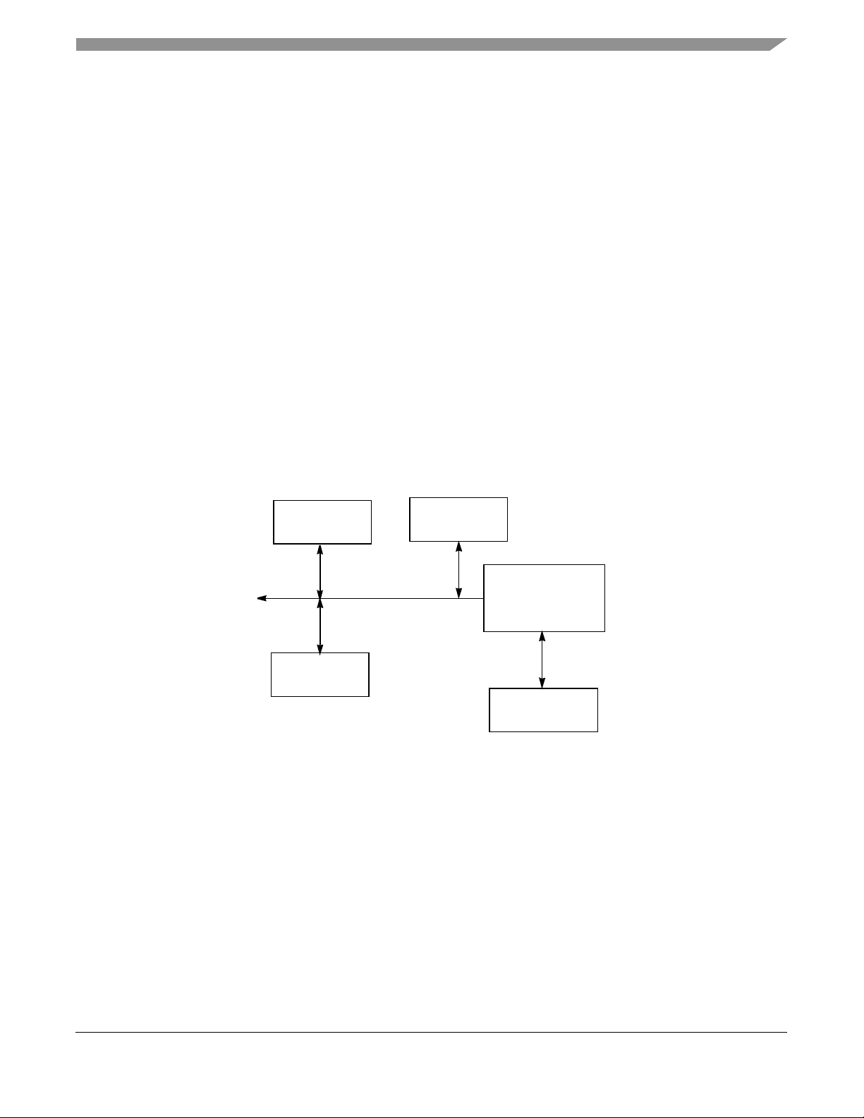
Overview
• 1.5V supply, 3.3V I/O
• 252MAP BGA, 21x 21mm package body size
• 1.0W power dissipation
1.4 Typical System Architecture
The MPC184 is designed to integrate easily into any system using the 8xx or PCI bus protocol.
The MPC184 is ideal in any system using a PowerQUICC communications processor (as shown
in Figure 1) or any system using PCI. The ability of the MPC184 to be a master on the 8xx bus
allows the co-processor to offload the data mov ement bottleneck normally as sociated with slave
devices.
The host processor accesses the MPC184 through its device drivers using system memory for data
storage. The MPC184 resides in the memory map of the processor, therefore when an application
requires cryptographic functions, it simply creates descriptors for the MPC184 which define the
cryptographic function to be performed and the location of the data. The MPC184’s mastering
capability permits the host processor to set up a crypto-channel with a few short register writes,
leaving the MPC184 to perform reads and writes on system memory to complete the required task.
EEPROM
Main
Memory
MPC184
8xx Bus
MPC860
I/O or Network
Interface
Figure 1-1. MPC184 Connected to PowerQuicc 8xx Bus
MPC184 Security Co-Processor User’s Manual: PCI Interface, Rev. 2
Freescale Semiconductor 1-3
Preliminary—Subject to Change Without Notice
Page 26
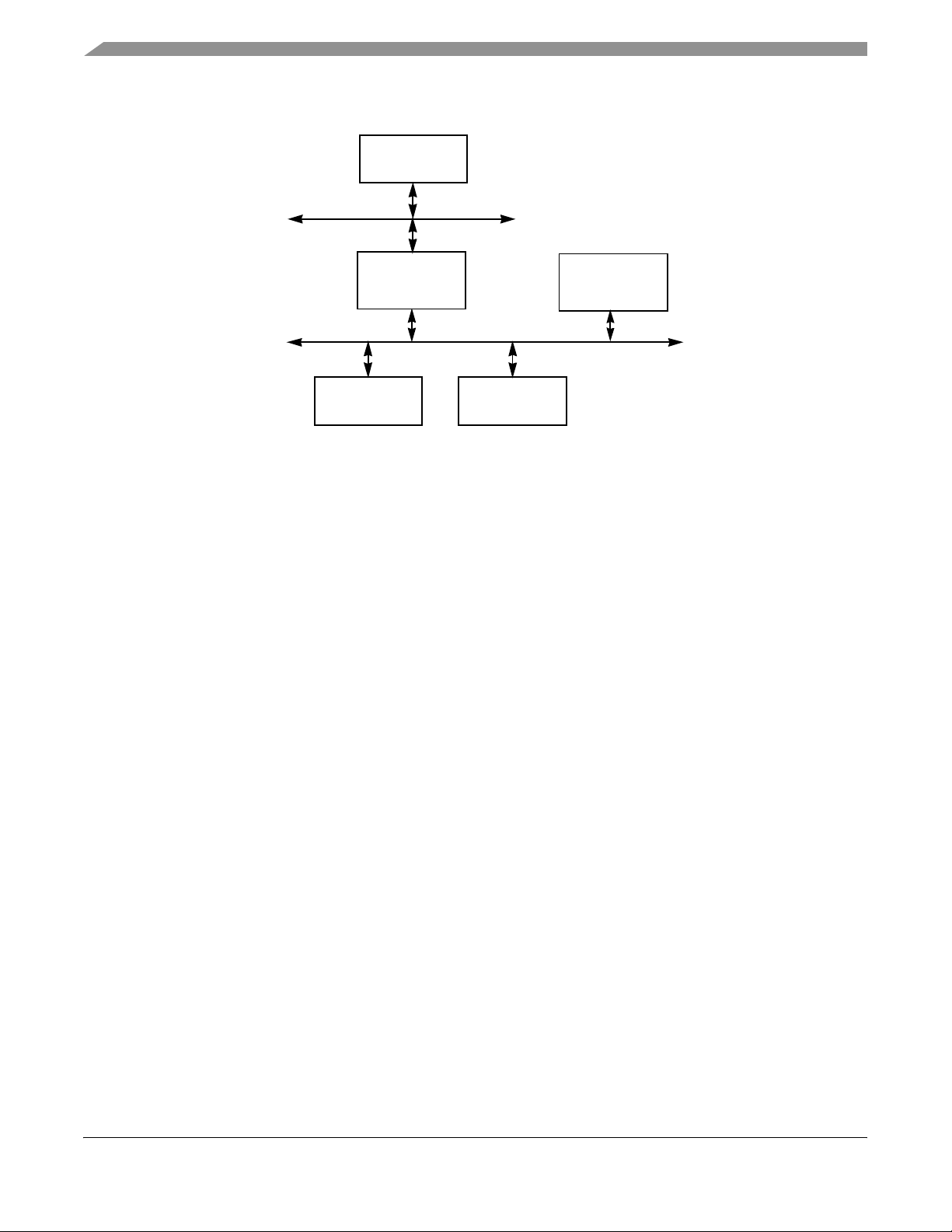
Overview
Main
Memory
Memory Bus
PCI Local Bus
Interface Card
MPC8245
Network
Network
Interface Card
MPC184
Figure 1-2. MPC184 Connected to host CPU via PCI bus
1.5 Architectural Overview
A block diagram of the MPC184 internal architecture is shown in Figure 1-1. The mode selectable
8xx/PCI bus interface module is designed to transfer 32-bit words between the external bus and
any register inside the MPC184. An operation begins with a write of a pointer to a crypto-channel
fetch register which points to a data packet descriptor. The channel then requests the descriptor and
decodes the operation to be performed. The channel then makes requests of the controller to assign
crypto execution units and fetch the keys, IV’s and data needed to perform the give n operation.
The controller satisfies the requests by assigning execution units to the channel and by making
requests to the master interface per the progr ammable priority scheme. As data is processed, it is
written to the individual execution units output buffer and then back to system memory via the bus
interface module.
MPC184 Security Co-Processor User’s Manual: PCI Interface, Rev. 2
1-4 Freescale Semiconductor
Preliminary—Subject to Change Without Notice
Page 27
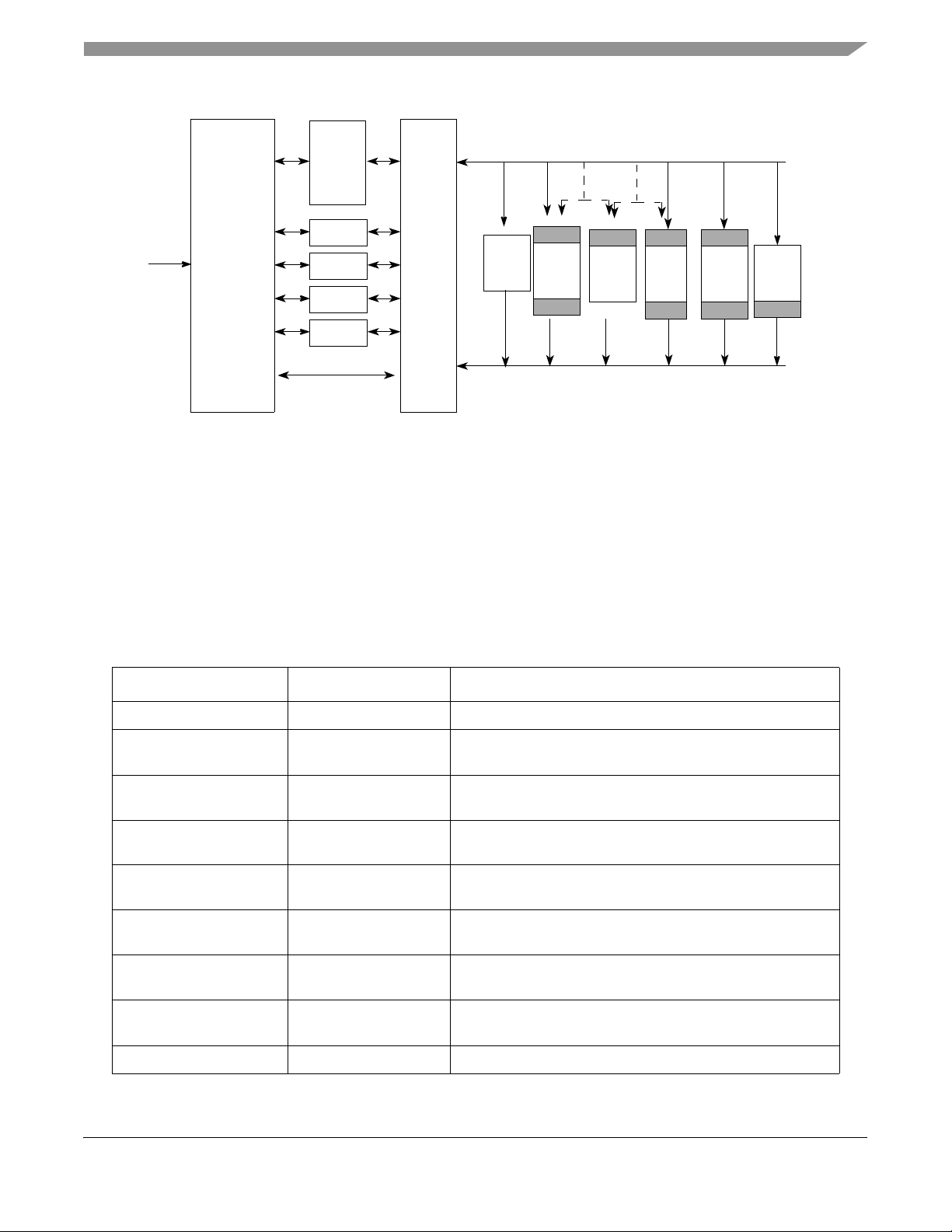
Overview
8KB
gpRAM
Master/slave
interface
cryptochannel
cryptochannel
cryptochannel
cryptochannel
Control
PKEU
FIFO
DEU
FIFO
FIFO
MDEU
FIFO
AES
FIFO
FIFO
ARC-4
FIFO
RNG
FIFO
Figure 1-3. MPC184 Functional Blocks
1.6 Data Packet Descriptors
As an IPSec accelerator, the MPC184’s controller has been designed for easy use and integration
with existing systems and software. All cryptographic functions are accessible through data packet
descriptors, some of which have been defined as multifunction to facilitate IPSec applications. A
data packet descriptor is diagrammed in Table 1-1.
Table 1-1. Example Data Packet Descriptor
Field Name Value/Type Description
DPD_DES_CTX_CRYPT TBD Representative header for DES using Context to Encrypt
LEN_CTXIN
PTR_CTXIN
LEN_KEY
PTR_KEY
LEN_DATAIN
PTR_DATAIN
LEN_DATAOUT
PTR_DATAOUT
LEN_CTXOUT
PTR_CTXOUT
Nul length
Nul pointer
Nul length
Nul pointer
Length
Pointer
Length
Pointer
Length
Pointer
Length
Pointer
Length
Pointer
Length
Pointer
Length
Pointer
Number of bytes to be written
Pointer to Context (IV) to be written into DES engine
Number of bytes in key
Pointer to block cipher key
Number of bytes of data to be ciphered
Pointer to data to perform cipher upon
Number of bytes of data after ciphering
Pointer to location where cipher output is to be written
Length of output Context (IV)
Pointer to location where altered Context is to be written
Zeroes for fixed length descriptor filter
Zeroes for fixed length descriptor filter
Zeroes for fixed length descriptor filter
Zeroes for fixed length descriptor filter
PTR_NEXT Pointer Pointer to next data packet descriptor
MPC184 Security Co-Processor User’s Manual: PCI Interface, Rev. 2
Freescale Semiconductor 1-5
Preliminary—Subject to Change Without Notice
Page 28

Overview
Each data packet descriptor contains the following:
• Header—The header describes the required services and encodes information that indicates
which EUs to use and which modes to set.
• Seven data length/data pointer pairs—The data length indicates the number of contiguous
bytes of data to be transferred. The data pointer indicates the starting address of the data,
key, or context in system memory .
• Next descriptor pointer
A data packet descriptor ends with a pointer to the next data packet descriptor. Therefore, once a
descriptor is processed and if the value of this pointer is non-zero, it is used to request a burst read
of the next descriptor.
Processing of the next descriptor (and whether or not a done signal is generated) is determined by
the programming of crypto-channel’s configuration register. Two modes of operation are
supported:
• Signal done at end of descriptor
• Signal done at end of descriptor chain
The crypto-channel can signal done via an interrupt or by a write-back of the descriptor header
after processing a data packet descriptor. The value written back is identical to that of the header,
with the exception that a DONE field is set.
Occasionally, a descriptor field may not be applicable to the requested service. For example, if
using DES in ECB mode, the contents of the IV field do not affect the result of the DES
computation. Therefore, when processing data packet descriptors, the crypto-channel skips any
pointer that has an associated length of zero.
1.6.1 External Bus Interface
The External Bus Interface (EBI) manages communication between the MPC184’s internal
execution units and the external bus. The interface is mode selectable between the PCI 2.2 bus
protocol, and the 8xx bus protocols, used by the PowerQuicc family of integrated communications
processors. The MPC184 is unique in its ability to act as a bus master on the 8xx bus. All on-chip
resources are memory mapped, and the target accesses and initiator writes from the MPC184 must
be addressed on word boundaries. The MPC184 will perform initiator reads on byte boundaries
and will adjust the data to place on word boundaries as appropriate. The bus mastering interface
allows the MPC184 t o off-load both crypto processing and data movement from the processor,
freeing the CPU for other networking system functions, allowing the chip set to achieve best in
class performance levels.
MPC184 Security Co-Processor User’s Manual: PCI Interface, Rev. 2
1-6 Freescale Semiconductor
Preliminary—Subject to Change Without Notice
Page 29

Overview
1.6.2 The MPC184 Controller
The MPC184 controller man ages on-chip resources, including ind ividual exe cution units (EUs),
FIFOs, the EBI, and the internal buses that connect all the various modules. The controller receives
service requests from the EBI and variou s crypto-channels, and schedules the required activities.
The controller can configure each of the on-chip resources in three modes:
• Host-controlled mode—The host is directly responsible for all data movement into and out
of the resource.
• Static mode—The user can reserve a specific execution unit to a specific crypto-channel.
• Dynamic mode—A crypto channel can request a particular service from any available
execution unit.
1.6.3 Host-Managed Register Access
All EUs can be used entirely through register read/write a ccess. It is strongly recommend ed that
read/write access only be performed on a EU that is statically assigned to an idle crypto-channel.
Such an assignment is the only method for the host to inform the controller that a particular EU is
in use.
1.6.4 Static EU Access
The Controller can be configured to reserve one or more EUs to a particular crypto-channel. Doing
so permits locking the EU to a particular context. When in this mode, the crypto-channel c an be
used by multiple descriptors representing the same context without unloading and reloading the
context at the end of each descriptor. This mode presents considerable performance improvement
over dynamic access, but only when the MPC184 is supporting a single context (or a single session
is being streamed.)
1.6.5 Dynamic EU Access
Processing begins when a data packet descriptor pointer is written to the next descriptor pointer
register of one of the crypto-channels. Prior to fetching the data referred to by the descriptor and
based on the services requested by the descriptor header in the descriptor buffer, the controller
dynamically reserves usage of an EU to the crypto-channel. If all appropriate EUs are already
dynamically reserved by other crypto-channels, the crypto-channel stalls and waits to fetch data
until the appropriate EU is available.
If multiple crypto-channels simultaneously request the same EU, the EU is assigned on a
round-robin basis. Once the required EU has been reserved, the crypto-channel fetches and loads
the appropriate data packets, operates the EU, unloads data to system memory , and releases the EU
for use by another crypto-channel. If a crypto-channel attempts to reserve a statically-assigned EU
(and no appropriate EUs are available for dynamic assignment), an interrupt is generated and
MPC184 Security Co-Processor User’s Manual: PCI Interface, Rev. 2
Freescale Semiconductor 1-7
Preliminary—Subject to Change Without Notice
Page 30

Overview
status indicates illegal access. When dynamic assignment is used, each encryption/decryption
packet must contain context that is particular to the context being supported.
1.6.6 Crypto-Channels
The MPC184 includes four crypto-channels that manage data and EU function. Each
crypto-channel consists of the following:
• Control registers containing information about the transaction in process
• A status register containing an indication of the last unfulfilled bus request
• A pointer register indicating the location of a new descriptor to fetch
• Buffer memory used to store the active data packet descriptor (See Section 1.6, “Data
Packet Descriptors.”)
Crypto-channels analyze the data packet descriptor header and request from the controller the first
required cryptographic service. The controller implements a programmable prioritization scheme
that allows the user to dictate the order in which the four crypto-channels are serviced. After the
controller grants access to the required EU, the crypto-channel and the controller perform the
following steps:
1. Set the appropriate Mode bits available in the EU for the required service.
2. Fetch context and other parameters as indicated in the data packet descriptor buffer and
use these to program the EU.
3. Fetch data as indicated and place in either the EU’s input FIFO or the EU itself (as
appropriate).
4. Wait for EU to complete processing.
5. Upon completion, unload results and context and write them to external memory as
indicated by the data packet descriptor buffer.
6. If multiple services requested, go back to step 2.
7. Reset the appropriate EU if it is dynamically assigned. Note that if statically assigned, a
EU is reset only upon direct command written to the MPC184.
8. Perform descriptor completion notification as appropriate. This notification comes in one
of two forms—interrupt or header writeback modification—and can occur either at the
end of every descriptor or at the end of a descriptor chain.
1.7 Execution Units (EUs)
“Execution unit” is the generic term for a functional block that performs the mathematical
permutations required by protocols used in cryptographic processing. The EUs are compatible
MPC184 Security Co-Processor User’s Manual: PCI Interface, Rev. 2
1-8 Freescale Semiconductor
Preliminary—Subject to Change Without Notice
Page 31

Overview
with IPSec, WAP/WTLS, IKE, SSL/TLS and 802.11i processing, and can work together to
perform high level cryptographic tasks.The MPC184’s execution units are as follows:
• PKEU for computing asymmetric key mathematics, including Modular Exponentiation
(and other Modular Arithmetic functions) or ECC Point Arithmetic
• DEU for performing block symmetric cryptography using DES and 3DES
• AFEU for performing RC-4 compatible stream symmetric cryptography
• AESU for performing the Advanced Encryption Standard algorithm
• MDEU for hashing data
• RNG for random number generation
1.7.1 Public Key Execution Unit (PKEU)
The PKEU is capable of performing many advanced mathematical functions to support both RSA
and ECC public key cryptographic algorithms. ECC is supported in both F(2)m
(polynomial-basis) and F(p) modes. This EU supports all levels of functions to assist the host
microprocessor to perform its desired cryptographic function. For exa mple, at the highest level,
the accelerator performs modular exponentiations to support RSA and perfo rms point mu ltiplies
to support ECC. At the lower levels, the PKEU can perform simple operations such as modular
multiplies.
1.7.1.1 Elliptic Curve Operations
The PKEU has its own data and control units, including a general-purpose register file in the
programmable-size arithmetic unit. The field or modulus size can be programmed to any value
between 160 bits and 512 bits in programmable increments of 8, with each programmable value i
supporting all actual field sizes from i*8 -7 to i*8. The result is hardware supporting a wide range
of cryptographic security. Larger field / modulus sizes result in greater security but lower
performance; processing time is determined by field or modulus size. For example, a field size of
160 is roughly equivalent to the security provided by 1024 bit RSA. A field size set to 208 roughly
equates to 2048 bits of RSA security.
The PKEU contains routines implementing the atomic functions for elliptic curve
processing—point arithmetic and finite field arithmetic. The point operations (multiplication,
addition and doubling) involve one or more finite field operations which are addition,
multiplication, inverse, and squaring. Point add and double each use of all four finite field
operations. Similarly, point multiplication uses all EC point operations as well as the finite field
operations. All these functions are supported both in modular arithmetic as well as polynomial
basis finite fields.
MPC184 Security Co-Processor User’s Manual: PCI Interface, Rev. 2
Freescale Semiconductor 1-9
Preliminary—Subject to Change Without Notice
Page 32

Overview
1.7.1.2 Modular Exponentiation Operations
The PKEU is also capable of performing ordinary integer modulo arithmetic. This arithmetic is an
integral part of the RSA public key algorithm; however, it can also play a role in the generation of
ECC digital signatures and Diffie-Hellman key exchanges.
Modular arithmetic functions supported by the MPC184’s PKEU include the following:
• R 2 mod N
• A’ E mod N
-1
• (A x B) R
• (A x B) R
• (A+B) mod N
• (A-B) mod N
mod N
-2
mod N
Where the following variable de finitions: A’ = AR mod N, N is the modulus vector, A and B are
s
input vectors, E is the exponent vector, R is 2
, where s is the bit length of the N vector rounded
up to the nearest multiple of 32.
The PKEU can perform m odular arithmetic on operands up to 2048 bits in length. The m odulus
must be larger than or equal to 129 bits. The PKEU uses the Montgomery modular multiplication
algorithm to perform core functions. The addition and subtraction functions exist to help support
known methods of the Chinese Remainder Theorem (CRT) for efficient exponentiation.
1.7.2 Data Encryption Standard Execution Unit (DEU)
The DES execution unit (DEU) performs bulk data encryption/decryption, in compliance with the
Data Encryption Standard algorithm (ANSI x3.92). The DEU can also compute 3DES and
extension of the DES al gorithm in which each 64-bit input block is processed three ti mes. The
MPC184 supports 2 key (K1=K3) or 3 key 3DES.
The DEU operates by permuting 64-bit data blocks with a shared 56-bit key and an initialization
vector (IV). The MPC184 supports two modes of IV operation: ECB (Electronic Code Book) and
CBC (Cipher Block Chaining).
1.7.3 Arc Four Execution Unit (AFEU)
The AFEU accelerates a bulk encryption algorithm compatible with the RC4 stream cipher from
RSA Security, Inc. The algorithm is byte-oriented, meaning a byte of plain text is encrypted with
a key to produce a byte of ciphertext. The key is variable length and the AFEU supports key
lengths from 40 to 128 bits (in byte increments), providing a wide range of security strengths. RC4
is a symmetric algorithm, meaning each of the two communicating parties share the same key.
MPC184 Security Co-Processor User’s Manual: PCI Interface, Rev. 2
1-10 Freescale Semiconductor
Preliminary—Subject to Change Without Notice
Page 33

Overview
1.7.4 Advanced Encryption Standard Execution Unit (AESU)
The AESU is used to accelerate bulk data encryption/decryption in compliance with the Advanced
Encryption Standard algorithm Rinjdael. The AESU executes on 128 bit blocks with a choice of
key sizes: 128, 192, or 256 bits.
AES is a symmetric key algori thm, the sender and receiver use the same key for both encryption
and decryption. The session key and IV(CBC mode) are supplied to the AESU module prior to
encryption. The processor supplies data to the module that is processed as 128 bit input. The
AESU operates in ECB, CBC, and counter modes.
1.7.5 Message Digest Execution Unit (MDEU) Module
The MDEU computes a single message digest (or hash or integrity check) value of all the data
presented on the input bus, using either the MD5, SHA-1 or SHA-256 algorithms for bulk data
hashing. With any hash algorithm, the larger message is mapped onto a smaller output space,
therefore collisions are potential, albeit not probable. The 160-bit hash value is a sufficiently large
space such that collisions are extremely rare. The security of the hash function is based on the
difficulty of locating collisions. That is, it is com putation infeasible to construct two distinct but
similar messages that produce the same hash output.
• The MD5 generates a 128-bit hash, and the algorithm is specified in RFC 1321.
• SHA-1 is a 160-bit hash function, specified by the ANSI X9.30-2 and FIPS 180-1
standards.
• SHA-256 is a 256-bit hash function that provides 256 bits of security against collision
attacks.
• The MDEU also supports HMAC computations, as specified in RFC 2104.
1.7.6 Random Number Generator (RNG)
The RNG is a digital integrated circuit capable of generating 32-bit random numbers. It is designed
to comply with FIPS 140-1 standards for randomness and non-determinism.
Because many cryptographic algorithms use random numbers as a source for generating a secret
value (a nonce), it is desirable to have a private RNG for use by the MPC184. The anonymity of
each random number must be maintained, as well as the unpredictability of the next random
number. The FIPS-140 compliant private RNG allows the system to develop random challenges
or random secret keys. The secret key can thus remain hidden from even the high-level application
code, providing an added measure of physical security.
MPC184 Security Co-Processor User’s Manual: PCI Interface, Rev. 2
Freescale Semiconductor 1-11
Preliminary—Subject to Change Without Notice
Page 34

Overview
1.7.7 8KB General Purpose RAM (gpRAM)
The MPC184 contains 8KB of internal general purpose RAM that can be used to store keys, IV’s
and data. The internal scratchpad allows the user to store frequently used context on chip which
increases system performance by minimizing setup time. This feature is especially important when
dealing with small packets and in systems where bus bandwidth is limited.
1.8 Performance Estimates
Bulk encryption/authentication performance estimates shown in Table 1-2. include
data/key/context reads (from memory to MPC184), security processing (internal to MPC184), and
writes of completed data/context to memory by MPC184, using typical bus overhead.
Table 1-2. Estimated Bulk Data Encryption Performance (Mbps)
DES
CBC
64 byte 43 36 38 32 43 38 34 29
128 byte 75 55 60 51 75 66 59 50
256 byte 119 76 83 70 118 100 87 74
512 byte 173 95 104 88 171 135 114 97
1024 byte 223 109 118 100 221 163 136 115
1536 byte 247 114 124 105 252 176 144 123
3DES
CBC
AES 128 AES 256 ARC4 MD5 SHA-1
3DES/
HMAC-
SHA-1(Rx)
The MPC184 supports single pass processing of encryption/message authentication. All
performance measurements assume descriptor generation and bus availability (66Mhz, 32bit PCI
bus with typical SDRAM read/write latency) are not constraints.
1.9 User’s Manual Revision History
A list of the major differences between revisions of the MPC184 Security Co-Processor User’s
Manual—PCI Interface, is provided in Appendix C, “User’s Manual Revision History.”
MPC184 Security Co-Processor User’s Manual: PCI Interface, Rev. 2
1-12 Freescale Semiconductor
Preliminary—Subject to Change Without Notice
Page 35

Chapter 2 Signal Descriptions
This chapter describes the signals used by the MPC184 in PCI mode, as well as the device pinout.
The MPC184 is designed to offer customers an easy migration path from the MPC190, the 32/64b
PCI Security Processor, in situations where the MPC190 is being used in 32-bit mode.
2.1 Signal Descriptions
Table 2-1 shows the signal descr iptions for the MPC184 in 32 bit PCI mode. The shaded regions
show the pins that MUST be No Connected in 32b PCI mode or must be taken into special
consideration for easy migration from the MPC190. Please also reference Chapter 2, 4 and 7 of the
PCI Local Bus Specification Revision 2.2 for other PCI system considerations.
Table 2-1. MPC184 PCI Signals
Signal
Name
AD[31:0] K2, K1, L2, L1, M2, M1, N2,
N1, R1, R2, T2, T3, T4, R5,
T5, R6, R12, T12, R13, T13,
R14, T14, T15, R15, P15,
P16, N15, N16, M15, M16,
C/BE[3-0]# P2, T6, T11, R16 I/O T/S Bus Command/Byte Enables
PAR R11 I/O T/S Parity (Even Parity across AD[31:0], C/BE [3:0]
FRAME# R7 I/O S/T/S Assertion of FRAME# by an Initiator indicates the
TRDY# R8 I/O S/T/S Assertion of TRDY# by a target indicates
IRDY# T7 I/O S/T/S Assertion of IRDY# by an Initiator indicates
Pin
Locations
L15, L16
Signal
Type
Address/Data and Command Pins (37)
I/O T/S Multiplexed Address/Data Bus
Interface Control (7)
Type Description
beginning of a bus transaction. FRAME is
deasserted 1 cycle before conclusion of the
transaction.
readiness to complete a bus transaction.
readiness to complete a bus transaction.
STOP# R9 I/O S/T/S Asserted by a target to request termination a bus
transaction.
MPC184 Security Co-Processor User’s Manual: PCI Interface, Rev. 2
Freescale Semiconductor 2-1
Preliminary—Subject to Change Without Notice
Page 36

Signal Descriptions
Table 2-1. MPC184 PCI Signals
Signal
Name
IDSEL P1 I IN Initialization device select is used as chip select
DEVSEL# T8 I/O S/T/S Asserted by a target when claiming a transaction
M66EN E2 I IN When asserted (at initialization time), the
PLL Bypass P5 I IN PLL Bypass
REQ# F1 O T/S Bus Request from Initiator to Arbiter
GNT# D2 I T/S Bus Grant from Arbiter to Initiator
CLK H1 I IN System Clock input
RST# E1 I IN Asynchronous reset signal. Initializes MPC184
Pin
Locations
Signal
Type
Arbitration (2)
System (3)
Type Description
pin during Type 0 configuration transactions.
(following subtractive decode of its address).
MPC184 enables its internal PLL to operate in
the 33-66MHz range.
0 (OVSS) = PLL Disabled
1 (OVDD) = PLL Enabled
to known state.
TPA G2 O Test Pad Analog
This pin MUST have No Connection
Error Reporting (2)
SERR# T10 O O/D System Error is active low when unrecoverable
system error is detected.
PERR# R10 I/O S/T/S Parity Error is active low when Parity Error is
detected
Interrupt Signals (1)
INTA# D1 O O/D Interrupt Request
JTAG/Boundary Scan (5)
TCK A3 I Test Clock
If JTAG is NOT used, this pin should be tied to
VSS
TDI C1 I Test Input
If JTAG is NOT used, this pin should be tied to
OVDD
TDO B1 O Test output
If JTAG is NOT used, this pin should be NC
MPC184 Security Co-Processor User’s Manual: PCI Interface, Rev. 2
2-2 Freescale Semiconductor
Preliminary—Subject to Change Without Notice
Page 37

Table 2-1. MPC184 PCI Signals
Signal Descriptions
Signal
Name
TMS A2 I Test Mode Select
TRST# A4 I Test Reset
Analog VDD F2 Analog PLL Power
AVSS H2 Analog PLL Ground
VSS B2, B3, B4, C2, C3, C4, C5,
C7, C10, C12, C13, C14, D3,
E14, F6, F7, F8, F9, F10, F11,
F14,G1, G3, G6, G7, G8, G9,
G10, G11, H6, H7, H8, H9,
H10, H11, J1, J2, J6, J7, J8,
J9, J10, J11, J14, K6, K7, K8,
K9, K10, K11, L3, L6, L7, L8,
L9, L10, L11, M14, N3, P3, P4,
P6, P7, P9, P11, P12, P13,
Pin
Locations
P14, R3, R4
Signal
Type
Powers/Grounds/No Connects (195)
Type Description
If JTAG is NOT used, this pin should be tied to
OVDD
If JTAG is NOT used, this pin should be tied to
VSS
MPC184 = +1.5 V
MPC190 = +1.8 V
Ground
IVDD E5, E6, E7, E8, E9, E10, E11,
E12, F5, F12, G5, G12, H5,
H12, J5, J12, K5, K12, L5,
L12, M5, M6, M7, M8, M9,
M10, M11, M12
OVDD C6, C8, C9, C11, D4, D5, D6,
D7, D8, D9, D10, D11, D12,
D13, D14, E3, E4, E13, F3,
F4, F13, G4, G13, G14, H3,
H4, H13, H14, J3, J4, J13, K3,
K4, K13, K14, L4, L13, L14,
M3, M4, M13, N4, N5, N6, N7,
N8, N9, N10, N11, N12, N13,
N14, P5, P8, P10, T9
NC G16, F15, F16, E15, E16,
D15, D16, C15, C16, B15,
B16, A15, B14, A14, B13,
A13, B12, A12, B11, A11,
B10, A10, B9, A9, B8, A8, B7,
A7, B6, A6, B5, A5, J15, J16,
H15, H16, G15, K16, K15
Core Power
MPC184 = +1.5 V
MPC190 = +1.8 V
I/O Power (+3.3v)
These pins MUST have No Connection
MPC184 Security Co-Processor User’s Manual: PCI Interface, Rev. 2
Freescale Semiconductor 2-3
Preliminary—Subject to Change Without Notice
Page 38

Signal Descriptions
2.2 MPC184 Pin Out
Figure 2-1 shows the pin connections for the MPC184 in 32 bit PCI mode. The shaded regions show the pins that
MUST be No Connected in 32b PCI mode or must be taken into special consideration for easy migration from the
MPC190.
1 2 3 4 5 6 7 8 9 10111213141516
A TMS TCK TRST
B TDO VSS VSS VSS
C TDI VSS VSS VSS VSS 3.3V VSS 3.3V 3.3V VSS 3.3V VSS VSS VSS
D INTA GNT VSS 3.3V 3.3V 3.3V 3.3V 3.3V 3.3V 3.3V 3.3V 3.3V 3.3V 3.3V
M66E
E RST#
F REQ#
G VSS
H CLK AVSS 3.3V 3.3V
J VSS VSS 3.3V 3.3V
3.3V 3.3V Core VCore VCore V Core VCore VCore VCore VCore V3.3V VSS NC NC E
N
Analo
3.3V 3.3V Core VVSS VSS VSS VSS VSS VSS Core V3.3V VSS NC NC F
gVdd
TPA
VSS 3.3V Core VVSS VSS VSS VSS VSS VSS Core V3.3V 3.3V NC NC G
/NC
NC NC NC NC NC NC NC NC NC NC NC A
NC NC NC NC NC NC NC NC NC NC NC NC B
Core VVSS VSS VSS VSS VSS VSS Core V3.3V 3.3V NC NC H
Core VVSS VSS VSS VSS VSS VSS Core V3.3V VSS NC NC J
NC NC C
NC NC D
K AD_30 AD_31 3.3V 3.3V
L AD_28 AD_29 VSS 3.3V
M AD_26 AD_27 3.3V 3.3V
N AD_24 AD_25VSS 3.3V 3.3V 3.3V 3.3V 3.3V 3.3V 3.3V 3.3V 3.3V 3.3V 3.3V AD_5 AD_4 N
Core VVSS VSS VSS VSS VSS VSS Core V3.3V 3.3V NC NC K
Core VVSS VSS VSS VSS VSS VSS Core V3.3V 3.3V AD_1 AD_0 L
Core VCore VCore V Core VCore VCore VCore VCore V3.3V VSS AD_3 AD_2 M
Figure 2-1. MPC184 Pinout
MPC184 Security Co-Processor User’s Manual: PCI Interface, Rev. 2
2-4 Freescale Semiconductor
Preliminary—Subject to Change Without Notice
Page 39

Signal Descriptions
1 2 3 4 5 6 7 8 9 10111213141516
P IDSE
C/BE_
VSS VSS
3
L
R AD_23 AD_22VSS VSS AD_18AD_1
PLL
Bypass
VSS VSS 3.3V VSS 3.3V VSS VSS VSS VSS AD_7 AD_6 P
FRAME
TRDY STOP PERR PAR AD_15 AD_13AD_11AD_8
6
T AD_21AD_20AD_19AD_1
7
C/BE_
2
IRDY
DEVSE
L
3.3V SERR
C/BE_
AD_14AD_12 AD_10AD_9 T
1
1 2 3 4 5 6 7 8 9 10111213141516
Figure 2-1. MPC184 Pinout
C/BE_
0
R
MPC184 Security Co-Processor User’s Manual: PCI Interface, Rev. 2
Freescale Semiconductor 2-5
Preliminary—Subject to Change Without Notice
Page 40

Signal Descriptions
MPC184 Security Co-Processor User’s Manual: PCI Interface, Rev. 2
2-6 Freescale Semiconductor
Preliminary—Subject to Change Without Notice
Page 41

Chapter 3 Address Map
This chapter contains the MPC184 address map. All registers are 32-bit aligned, and are addressed
on 32-bit boundaries.
The MPC184’s internal memory resources are within a contiguous block of mem ory. The size of
the internal space is 128
PCI protocol.
3.1 Address Map
Table 3-1 shows the base address map, and Table 3-2 the precise address map, including all
registers in the Execution Units. The 17-bit MPC184 address bus value is shown. Note that these
tables show module addresses; the 3 least significant address bits that are used to select bytes
within 32-bit-words are not shown.
Kbytes. In PCI mode, the Base Address Register is set according to the
Table 3-1. Module Base Address Map
MPC184 Address
(hex) (AD 16::0)
00000-00 FFF Configurat ion MPC184 Configuration Setup Configuration
01000-01FFF Controller Arbiter/Controller Control Register Space Resource Control
02000-02FFF Channel 1 Crypto-Channel unit 1 Data Control
03000-03FFF Channel 2 Crypto-Channel unit 2 Data Control
04000-04FFF Channel 3 Crypto-Channel unit 3 Data Control
05000-05FFF Channel 4 Crypto-Channel unit 4 Data Control
08000-08 FFF AFEU ARCFour Execution Unit CryptoAccelerator
0A000-0AFFF DEU DES Execution Unit CryptoAccelerator
0C000 -0 C FFF MDEU Messa ge Digest Execution Unit CryptoAccelerator
0E000-0EFFF RNG Random Number Generator CryptoAccelerator
10000-10 FFF PKEU Public Key Execution Unit CryptoAccelerator
12000-12FFF AESU AES Execution Unit CryptoAccelerator
18000-19FFF Memory 8K Bytes General Purpose Memory Memory
MPC184 Module Description Type
Table 3-2 shows the system address map including all functional registers.
MPC184 Security Co-Processor User’s Manual: PCI Interface, Rev. 2
Freescale Semiconductor 3-1
Preliminary—Subject to Change Without Notice
Page 42

Address Map
Table 3-2. Preliminary System Address Map Showing All Registers
MPC184 Address
(hex) (AD 16::0)
00F00 Configuration 8xx Mode Base Address R/W
00800 Configuration 8xx Slave PERR Address R
01000 Controller EU Assignment Control R/W
01008 Controller Interrupt Mask R/W
01010 Controller Interrupt Status R
01018 Controller Interrupt Clear W
01024 Controller Identification R
01028 Controller EU Assignment Status R
01030 Controller Master Control R/W
01038 Controller Master TEA Address (8xx mode only) R
02008 Channel_1 Config register R/W
02010 Channel_1 Pointer status R
02040 Channel_1 Current descriptor pointer R
02048 Channel_1 Fetch register R/W
02080-020BF Channel_1 Descriptor buffer[16] R/W
MPC184 Module Description Type
03008 Channel_2 Config register R/W
03010 Channel_2 Pointer status R
03040 Channel_2 Current descriptor pointer R
03048 Channel_2 Fetch register R/W
03080-030BF Channel_2 Descriptor buffer[16] R/W
04008 Channel_3 Config register R/W
04010 Channel_3 Pointer status R
04040 Channel_3 Current descriptor pointer R
04048 Channel_3 Fetch register R/W
04080-040BF Channel_3 Descriptor buffer[16] R/W
05008 Channel_4 Config register R/W
05010 Channel_4 Pointer status R
05040 Channel_4 Current descriptor pointer R
05048 Channel_4 Fetch register R/W
05080-050BF Channel_4 Descriptor buffer[16] R/W
08000 AFEU Mode Register R/W
08008 AFEU Key Size Register R/W
MPC184 Security Co-Processor User’s Manual: PCI Interface, Rev. 2
3-2 Freescale Semiconductor
Preliminary—Subject to Change Without Notice
Page 43

Address Map
Table 3-2. Preliminary System Address Map Showing All Registers (continued)
MPC184 Address
(hex) (AD 16::0)
08010 AFEU Context/Data Size Register R/W
08018 AFEU Reset Control Register R/W
08028 AFEU Status Register R
08030 AFEU Interrupt Status Register R/W
08038 AFEU Interrupt Control Register R/W
08050 AFEU End of Message Register W
08100-081FF AFEU Context Memory R/W
08200 AFEU Context Memory Pointers R/W
08400 AFEU Key Register 0 W
08408 AFEU Key Register 1 W
08800-08FFF AFEU FIFO R/W
0A000 DEU Mode Register R/W
0A008 DEU Key Size Register R/W
0A010 DEU Data Size Register R/W
0A018 DEU Reset Control Register R/W
MPC184 Module Description Type
0A028 DEU Status Register R
0A030 DEU Interrupt Status Register R/W
0A038 DEU Interrupt Control Register R/W
0A050 DEU EU-Go W
0A100 DEU IV Register R/W
0A400 DEU Key 1 Register W
0A408 DEU Key 2 Register W
0A410 DEU Key 3 Register W
0A800-0AFFF DEU FIFO R/W
OC000 MDEU Mode Register R/W
0C008 MDEU Key Size Register R/W
0C010 MDEU Data Size Register R/W
0C018 MDEU Reset Control Register R/W
0C028 MDEU Status Register R
0C030 MDEU Interrupt Status Register R/W
0C038 MDEU Interrupt Control Register R/W
0C050 MDEU EU_GO W
MPC184 Security Co-Processor User’s Manual: PCI Interface, Rev. 2
Freescale Semiconductor 3-3
Preliminary—Subject to Change Without Notice
Page 44

Address Map
Table 3-2. Preliminary System Address Map Showing All Registers (continued)
MPC184 Address
(hex) (AD 16::0)
0C100-0C120 MDEU Context Memory R/W
0C400-0C47F MDEU Key Memory W
0C800-0CFFF MDEU FIFO W
0E000 RNG Mode Register R/W
0E010 RNG Data Size Register R/W
0E018 RNG Reset Control Register R/W
0E028 RNG Status Register R
0E030 RNG Interrupt Status Register R/W
0E038 RNG Interrupt Control Register R/W
0E050 RNG EU_GO W
0E800-0EFFF RNG FIFO R
10000 PKEU Mode Register R/W
10008 PKEU Key Size Register R/W
10010 PKEU Data Size Register R/W
10018 PKEU Reset Control Register R/W
MPC184 Module Description Type
10028 PKEU Status Register R
10030 PKEU Interrupt Status Register R/W
10038 PKEU Interrupt Control Register R/W
10050 PKEU EU_GO W
10200-1023F PKEU Parameter Memory A0 R/W
10240-1027F PKEU Parameter Memory A1 R/W
10280-102BF PKEU Parameter Memory A2 R/W
102C0-102FF PKEU Parameter Memory A3 R/W
10300-1033F PKEU Parameter Memory B0 R/W
10340-1037F PKEU Parameter Memory B1 R/W
10380-103BF PKEU Parameter Memory B2 R/W
103C0-103FF PKEU Parameter Memory B3 R/W
10400-104FF PKEU Parameter Memory E W
10800-108FF PKEU Parameter Memory N R/W
12000 AESU Mode Register R/W
12008 AESU Key Size Register R/W
12010 AESU Data Size Register R/W
MPC184 Security Co-Processor User’s Manual: PCI Interface, Rev. 2
3-4 Freescale Semiconductor
Preliminary—Subject to Change Without Notice
Page 45

Address Map
Table 3-2. Preliminary System Address Map Showing All Registers (continued)
MPC184 Address
(hex) (AD 16::0)
12018 AESU Reset Control Register R/W
12028 AESU Status Register R
12030 AESU Interrupt Status Register R/W
12038 AESU Interrupt Control Register R/W
12050 AESU End of Message Register W
12100 AESU IV Register R/W
12400-12408 AESU Key Memory R/W
12800-12FFF AESU FIFO R/W
18000-19FFF Memory General Purpose Memory R/W
MPC184 Module Description Type
MPC184 Security Co-Processor User’s Manual: PCI Interface, Rev. 2
Freescale Semiconductor 3-5
Preliminary—Subject to Change Without Notice
Page 46

Address Map
MPC184 Security Co-Processor User’s Manual: PCI Interface, Rev. 2
3-6 Freescale Semiconductor
Preliminary—Subject to Change Without Notice
Page 47

Chapter 4 PCI Configuration Registers
The MPC184 is a PCI 2.2-compliant device. All PCI configuration space register names are
defined in the PCI Local Bus Specification, Revision 2.2, December 18, 1998. Per the PCI Local
Bus Specification, 32-bits is referred to as a DWORD.
4.1 PCI Configuration Space
The MPC184 uses a Type 00h configuration space header with one base address register.
Name
(Reset)
31 24 23 16 15 8 7 0
Device ID (0x6405) Vendor ID (0x1057) 0x000
Status (0x02A0) Command (0x0000) 0x004
Class Code (0x1000_00) Revision ID (0x00) 0x008
BIST (0x00) Header Type (0x00) Latency Timer (0x00) Cache Line Size
(0x00)
BAR 0 (0x0000_0008) 0x010
BAR 1 (0x0000_0000) 0x014
BAR 2 (0x0000_0000) 0x018
BAR 3 (0x0000_0008) 0x01C
BAR 4 (0x0000_0000) 0x020
BAR 5 (0x0000_0000) 0x024
Cardbus CIS Pointer (0x0000_0000) 0x028
Subsystem ID (0x0000) Subsystem Vendor ID (0x0000) 0x02C
Expansion ROM Base Address (0x0000_0000) 0x030
Reserved (0x0000_00) Capabilities Pointer
(0x00)
Offset
0x00C
0x034
Reserved (0x0000_0000) 0x038
Max_LAT (0x00) Min_GNT (0x00) Interrupt Pin (0x01) Interrupt Line (0x00) 0x03C
Figure 4-1. PCI Type 00h Configuration Space Header
MPC184 Security Co-Processor User’s Manual: PCI Interface, Rev. 2
Freescale Semiconductor 4-1
Preliminary—Subject to Change Without Notice
Page 48

PCI Configuration Registers
4.1.1 PCI Vendor ID Register (offset 0x0000)
The first DWORD in the configuration space header contains the read only PCI vendor ID register .
This two-byte register contains the value 0x1057.
15 0
Signal Device ID
Reset 0x1057
R/W Read Only
Figure 4-2. PCI Vendor ID Register
4.1.2 PCI Device ID Register (offset 0x0002)
The first DWORD in the configuration space header also contains the read only PC I device ID
register. This two-byte register contains the value 0x6405.
31 16
Signal Device ID
Reset 0x6405
R/W Read Only
Figure 4-3. PCI Device ID Register
4.1.3 PCI Command Register (offset 0x0004)
The second DWORD in the configuration space header contains the R/W PCI command register.
This two-byte register resets to the value 0x0000. The recommended setting for this register is
0x0146.
15 109876543210
Field F S ST PE V MW SP B M IO
Reset 0x0000
Recommended 0x0146
R/W R/W
Figure 4-4. PCI Command Register
Table 4-1 defines PCI command register signals.
MPC184 Security Co-Processor User’s Manual: PCI Interface, Rev. 2
4-2 Freescale Semiconductor
Preliminary—Subject to Change Without Notice
Page 49

Table 4-1. PCI Command Register Signals
PCI Configuration Registers
Bits R/W Name
15:10 R — 0 Reserved
9 R/W F 0 Fast-back-to-back enable. As a master, the MPC184 does not perform fast
8 R/W S 1 SERR# enable. The MPC184 optionally supports SERR# reporting.
7 R/W St 0 Stepping control. The MPC184 does not support address/data stepping.
6 R/W PE 1 Parity error response. Enables PERR# reporting on the MPC184.
5 R/W V 0 VGA palette snoop enable. Not a display device.
4 R/W MW 0 Memory write and invalidate enable. As a master, the MPC184 does not use
3 R/W SP 0 Special Cycles. The MPC184 does not support special cycles.
2 R/W B 1 Bus Master. The MPC184 should be operated primarily as a bus master.
1 R/W M 1 Memory Space. MPC184 is a memory space decoder.
0 R/W IO 0 IO Space. MPC184 does not support IO address space.
Recommended
Value
Description
back-to-back transactions.
the mem write and invalidate command.
4.1.4 PCI Status Register (offset 0x0006)
The second DWORD in the configuration space header also conta ins the read only PCI status
register. This 2 byte register resets to the value 0x02A0.
31 30 29 28 27 26 25 24 23 22 21 20 19 16
Field PE SE MA TR TS DT DP F R 66M C —
Reset 0x02A0
Recommended NA
R/W Read Only
Figure 4-5. PCI Status Register
Table 4-2 defines PCI status register signals.
Table 4-2. PCI Status Register Signals
Bits R/W Name Reset Value Description
31 R/W PE 0 Detected parity error. MPC184-detected parity error
30 R/W SE 0 Signaled system error. MPC184-signalled SERR#
29 R/W MA 0 Master abort. MPC184 terminated a transaction with a master abort.
28 R/W TR 0 Received target abort. Target currently addressed by MPC184-terminated
transaction with target abort.
MPC184 Security Co-Processor User’s Manual: PCI Interface, Rev. 2
Freescale Semiconductor 4-3
Preliminary—Subject to Change Without Notice
Page 50

PCI Configuration Registers
Table 4-2. PCI Status Register Signals (continued)
Bits R/W Name Reset Value Description
27 R/W TS 0 Signaled target abort. MPC184, as the currently addressed target, has
terminated a transaction with a target abort.
26:25 R DT 01 Device select timing. As a target, the MPC184 is medium address decoder.
24 R/W DP 0 Master data parity error. While operating as a master, the MPC184 detected
a data parity error.
23 R F 1 Fast back-to-back capable. MPC184 is a fast back-to-back capable target.
22 R Reserved 0 Reserved, hardwired to zero
21 R 66M 1 66MHz capable. The MPC184 is 66MHz capable.
20 R C 0 Capabilities list. No extended capabilities supported
19:16 R Reserved 0000 Reserved, hardwired to zero
4.1.5 Revision ID Register (offset 0x0008)
The third DWORD in the configuration space header contains the read only revision ID register.
This one-byte register resets to the value 0x00, indicating this is the first revision of the MPC184.
4.1.6 Class Code Register (offset 0x0009)
The third DWORD in the configuration space header also contains the read-only class code
register. This three-byte register resets to the value 0x1000_00, indicating that the MPC184
belongs to the PCI device category known as “Encryption/Decryption Controller/Network and
Computing Encrypt/Decrypt.”
31 87 0
Field Class Code Register Revision ID
Reset 0x1000_00 0x00
Recommended NA
R/W Read Only
Figure 4-6. Revision ID/Class Code Register
4.1.7 Cache Line Size Register (offset 0x000C)
The fourth DWORD in the configuration space header contains the R/W cache line size register.
This one-byte register resets to the value 0x00, indicating that memory write and invalidate
commands are not supported.
MPC184 Security Co-Processor User’s Manual: PCI Interface, Rev. 2
4-4 Freescale Semiconductor
Preliminary—Subject to Change Without Notice
Page 51

PCI Configuration Registers
4.1.8 Latency Timer Register (offset 0x000D)
The fourth DWORD in the configuration space header also contains the R/W latency timer
register. This one-byte register resets to the value 0x00; however, it is recommended that this
register be set to 0x10. This indicates that the MPC184 will achieve best performance when
granted mastership of the PCI bus for at least 32 PCI clocks. The MPC184 will typically make
several short reads or writes during context switching, followed by long reads and writes for data
movement.
4.1.9 Header-Type Register (offset 0x000E)
The fourth DWORD in the configuration space header also contains the R/W header type register.
This one-byte register resets to the value 0x00, indicating that the MPC184 uses a type 0 PCI
Configuration Header.
4.1.10 BIST Register (offset 0x000F)
The fourth DWORD in the configuration space header also contains the R/W BIST register. This
one-byte register resets to the value 0x00, indicating that the MPC184 does not implement BIST.
31 24 23 16 15 8 7 0
Field BIST Header Type Latency Timer Cache LIne SIze
Reset 0x00 0x00 0x00 0x00
Recommended 0x0000_1000
R/W R/W
Figure 4-7. Cache Line/Latency Timer/Header Type/BIST
4.1.11 Base Address Register Zero (offset 0x0010)
The fifth DWORD in the configuration space header contains the R/W base address register zero.
This four-byte register resets to the value 0x0000_0008. The base address registers define the
memory address range that the MPC184 will decode and respond to with the assertion of
DEVSEL. Base Address Registers 0 - 3 are implemented. Base addresses 1 to 3 shou ld be equal
to Base Address 0 plus 0x08000, 0x10000, and 0x18000 respectively . Also Base Address 0 and 3
are pre-fetchable, Base Address 1 and 2 are not pre-fetchable.
MPC184 Security Co-Processor User’s Manual: PCI Interface, Rev. 2
Freescale Semiconductor 4-5
Preliminary—Subject to Change Without Notice
Page 52

PCI Configuration Registers
31 43210
Field BAR0 TA CR TS
Reset 0x0000_000 1 00 0
Recommended 0x0000_0000
R/W R/W
Figure 4-8. Base Address Register 0
Table 4-3. Base Address Register 0 Signals
Bits R/W Name Reset Value Description
31:17 R/W BAR_0 0x0000 Base address
16:4 R/W — 0x000 Reserved
3 taccess b1 Prefetchable attribute bit. Indicates that the MPC184 is pre-fetchable.
2:1 R/W crange b00 Decoder width field. Locates MPC184 address map anywhere in lower 4GB of
memory addresses
0 R/W tspace b0 Indicates that the MPC184 decodes its address in memory spaces
Note: Bit 3, “taccess,” is hardwired to 1, indicating that this portion of the MPC184 address map is pre-fetchable.
4.1.12 Base Address Register 1 (offset 0x0014)
Base address register 1 is implemented, and defines a segment of the MPC184 address map that is
not pre-fetchable. This Base address should be equal to Base Address 0 plus 0x08000. Reads of
this register return 0x0000_0000 at reset.
4.1.13 Base Address Register 2 (offset 0x0018)
Base address register 2 is implemented, and defines a segment of the MPC184 address map that is
not pre-fetchable. This Base address should be equal to Base address 0 plus 0x10000. Reads of
this register return 0x0000_0000 at reset.
4.1.14 Base Address Register 3 (offset 0x001C)
Base address register 3 is implemented. Reads of this register return 0x0000_0008, indicating that
this portion of the MPC184 address map is well behaved, pre-fetchable memory. This Base
address should be equal to Base address 0 plus 0x18000. Reads of this register return
0x0000_0008 at reset.
4.1.15 Base Address Register 4 (offset 0x0020)
Base address register 4 is not implemented. Reads of this register return 0x0000_0000.
MPC184 Security Co-Processor User’s Manual: PCI Interface, Rev. 2
4-6 Freescale Semiconductor
Preliminary—Subject to Change Without Notice
Page 53

PCI Configuration Registers
4.1.16 Base Address Register 5 (offset 0x0024)
Base address register 5 is not implemented. Reads of this register return 0x0000_0000.
31 0
Field BAR4–5
Reset 0
Recommended NA
R/W R/W
Figure 4-9. Base Address Registers 4-5
4.1.17 CardBus CIS Pointer Register (offset 0x0028)
The eleventh DWORD in the configuration space header contains the R/W CardBus CIS pointer
register. This four-byte register resets to the value 0x0000_0000, indica ting that CardBus CIS
pointer is not implemented.
31 0
Field CardBus CIS Pointer
Reset 0x0000_0000
Recommended NA
R/W R/W
Figure 4-10. CardBus CIS Pointer Register
4.1.18 Subsystem Vendor ID Register (offset 0x002C)
The twelfth DWORD in the configuration space header contains t he read only subsystem vendor
ID register. This two-byte register contains the value 0x0000.
4.1.19 Subsystem ID Register (offset 0x002E)
The twelfth DWORD in the configuration space header also contains the read only subsystem ID
register. This two-byte register contains the value 0x0000.
31 16 15 0
Field Subsystem ID Subsystem Vendor ID
Reset 0x0000 0x0000
Recommended NA
R/W Read Only
Figure 4-11. Subsystem ID Registers
MPC184 Security Co-Processor User’s Manual: PCI Interface, Rev. 2
Freescale Semiconductor 4-7
Preliminary—Subject to Change Without Notice
Page 54

PCI Configuration Registers
4.1.20 Expansion ROM Base Address Register (offset 0x0030)
The thirteenth DWORD in the configuration space header contains the R/W expansion ROM base
address register. This four-byte register resets to the value 0x0000_0000, indicating that expansion
ROM base address is not implemented.
31 0
Field Expansion ROM Base Address
Reset 0x0000_0000
Recommended NA
R/W R/W
Figure 4-12. Expansion ROM Base Address Register
4.1.21 Capabilities Pointer (offset 0x0034)
The fourteenth DWORD in the configuration space header contains the R/W capabilities pointer
register. This one-byte register resets to the value 0x00, indicating the MPC184 has no extended
PCI capabilities. The remainder of this DWORD is reserved.
31 87 0
Field — Capabilities Pointer
Reset 0x0000_00 0x00
Recommended NA
R/W R/W
Figure 4-13. Capabilities Pointer
4.1.22 Interrupt Line Register (offset 0x003C)
The sixteenth DWORD in the configuration space header contains the read only interrupt line
register. This one-byte register rese ts to the value 0x00, indicating that interrupt routing has not
yet been assigned to the function.
4.1.23 Interrupt Pin Register (offset 0x003D)
The sixteenth DWORD in the configuration space header also contains the read only interrupt pin
register . This one-byte register resets to the value 0x01, which selects INTA#.
4.1.24 Min_GNT Register (offset 0x003D)
The sixteenth DWORD in t he configuration space header also contains the read only M in_GNT
register . This one-byte register resets to the value 0x00.
MPC184 Security Co-Processor User’s Manual: PCI Interface, Rev. 2
4-8 Freescale Semiconductor
Preliminary—Subject to Change Without Notice
Page 55

PCI Configuration Registers
4.1.25 Max_Lat Register (offset 0x003F)
The sixteenth DWORD in the configuration space header also contains the read only Max_Lat
register . This one-byte register resets to the value 0x00.
31 24 23 16 15 8 7 0
Field Max_Lat Min_GNT Interrupt Pin Interrupt Line
Reset 0x00 0x00 0x01 0x00
Recommended NA
R/W Read Only
Figure 4-14. Registers of the Sixteenth D-Word
MPC184 Security Co-Processor User’s Manual: PCI Interface, Rev. 2
Freescale Semiconductor 4-9
Preliminary—Subject to Change Without Notice
Page 56

PCI Configuration Registers
MPC184 Security Co-Processor User’s Manual: PCI Interface, Rev. 2
4-10 Freescale Semiconductor
Preliminary—Subject to Change Without Notice
Page 57

Chapter 5 Execution Units
“Execution unit” is the generic term for a functional block that performs the mathematical
permutations required by protocols used in cryptographic processing. The EUs are compatible
with IPsec, WAP/WTLS, IKE, SSL/TLS and DOCSIS BPI++ processing, and can work together
to perform high level cryptographic tasks.
The following Execution Units are used on the MPC184:
• Public Key Execution Unit (PKEU) supporting:
— RSA and Diffie-Hellman
— Elliptic curve operations in either F
• Data Encryption Standard Execution Unit (DEU) supporting:
—DES
—3DES
— Two key (K1, K2, K1) or Three Key (K1, K2, K3)
— ECB and CBC modes for both DES and 3DES
• Advanced Encryption Standard Execution Unit (AESU) supporting:
— 128, 192, or 256 bit keys
— ECB, CBC, and Counter modes for all key lengths
• ARC Four Execution Unit (AFEU)
— Implements a stream cipher compatible with the RC-4 algorithm
— 8- to 128-bit programmable key
• Message Digest Execution Unit (MDEU) supporting:
— SHA-1, a 160 bit hash function, specified by the ANSI X9.30-2 and FIPS 180-1
standards.
— The MD5 generates a 128 bit hash, and the algorithm is specified in RFC 1321.
m or F
2
p
— SHA-256, a 256-bit hash function that provides 256 bits of security against collision
attacks.
— The MDEU also supports HMAC computations, as specified in RFC 2104.
• Private on-chip random number generator (RNG)
MPC184 Security Co-Processor User’s Manual: PCI Interface, Rev. 2
Freescale Semiconductor 5-1
Preliminary—Subject to Change Without Notice
Page 58

Execution Units
Working together, the EUs can perform high-level cryptographic tasks, such as IPSec
encapsulating security protocol (ESP) and digital signature. The remainder of this Chapter
provides details about the Execution Units themselves.
5.1 Public Key Execution Units (PKEU)
This section contains details about the Public Key Execution Unit (PKEU), including detailed
register map, modes of operation, status and control registers, and the parameter RAMs.
5.1.1 PKEU Register Map
The PKEU contains the following registers and parameter memories, which are explained in detail
in the following sections.
• PKEU Mode Register
• Key Size Register
• Data Size Register
• Reset Control Register
• Status Register
• Interrupt Status Register
• Interrupt Control Register
• “Go” Register
• Parameter Memory A
• Parameter Memory B
• Parameter Memory E
• Parameter Memory N
5.1.2 PKEU Mode Register
This register specifies the internal PKEU routine to be executed. For the root arithmetic routines,
PKEU has the capability to perform arithmetic operations on subsegments of the entire memory.
This is particularly useful for operations such as ECDH (elliptic curve Diffie-Hellman) key
agreement computation. By using regAsel and regBsel, for example, parameter memory A
subsegment 2 can be multiplied into parameter memory B subsegment 1. Figure 5-1 and
Figure 5-2 detail two definitions.
MPC184 Security Co-Processor User’s Manual: PCI Interface, Rev. 2
5-2 Freescale Semiconductor
Preliminary—Subject to Change Without Notice
Page 59

31 76 0
Field Reserved MODE
Execution Units
Reset 0
0
R/W R/W
Addr PKEU 0x10000
31 0
Field Reserved
Reset 0
R/W R/W
Addr PKEU 0x10004
Figure 5-1. PKEU Mode Register: Definition 1
31 76430
Field Reserved MODE REGSEL
Reset 0
R/W R/W
Addr PKEU 0x10000
31 0
Field Reserved
00
Reset 0
R/W R/W
Addr PKEU 0x10004
Figure 5-2. PKEU Mode Register: Definition 2
Table 5-1 lists mode register routine definitions. Parameter memories are referred to for the base
address, as show.
Table 5-1. Mode Register Routine Definitions
Routine Mode [6:4] Mode [3:2] Mode [1:0]
Reserved 000 00 00
Clea r Me m o ry 000 0 01
Modular Exponentiation 000 00 10
2
R
mod N 000 00 11
R
mod N 000 01 00
nRp
F
Affine Point Mu ltiplication 000 01 01
p
F
m Affi ne P o int Multiplication 000 01 10
2
MPC184 Security Co-Processor User’s Manual: PCI Interface, Rev. 2
Freescale Semiconductor 5-3
Preliminary—Subject to Change Without Notice
Page 60

Execution Units
Fp Projective Point Multi p lication 000 01 11
F
m Projective Point Multiplication 000 10 00
2
F
Point Addition 000 10 01
p
F
Point Doubling 000 10 10
p
F
m Point Addition 000 10 11
2
F
m Point Doubling 000 11 00
2
F
m R2 CMD 000 11 01
2
F
m INV CMD 000 11 10
2
MOD INV CMD 000 11 11
Modular Addition 001 regAsel
Table 5-1. Mode Register Routine Definitions (continued)
Routine Mode [6:4] Mode [3:2] Mode [1:0]
1
regBsel
1
Modular Subtraction 010
Modular Multiplication with single Reduction 011
Modular Mult iplication with double Reducti on 100
Polynomial A ddition 101
Polyno mial Multiplication with si n gle Reduction 110
Polynomial Multiplica tion with double Reduction 111
1
regAsel and regBsel here refer to the specific segment of Parameter Memory A and B.
00 = A0
01 = A1
10 = A2
11 = A3
00 = B0
01 = B1
10 = B2
11 = B3
5.1.3 PKEU Key Size Register
The Key Size Register reflects the number of significant bytes to be used from PKEU Parameter
Memory E in performing modular exponentiation or elliptic curve point multiplication. The
minimum value for this register, when performing either modular exponentiation or elliptic curve
point multiplication, is 1 byte. The maximum legal value is 256 bytes. To avoid a key size error,
31:9 must be set to zero, and the value of 8:0 must not be greater than 256.
MPC184 Security Co-Processor User’s Manual: PCI Interface, Rev. 2
5-4 Freescale Semiconductor
Preliminary—Subject to Change Without Notice
Page 61

Execution Units
31 80
Field RESERVED Key Size
Reset 0
R/W R/W
Addr PKEU 0x10008
31 0
Field RESERVED
Reset 0
R/W R/W
Addr PKEU 0x1000C
Figure 5-3. PKEU Key Size Register
5.1.4 PKEU Data Size Register
The PKEU Data Size Register specifies, in bits, the size of the significant portion of the modulus
or irreducible polynomial. Any value written to this register that is a multiple of 32 bits (i.e. 128
bits, 160 bits,...), will be represented internally as the same value (128 bits, 160 bits,...). Any value
written that is not a multiple of 32 bits (i.e. 132bits, 161bits,...), will be represented in ternally as
the next larger 32 bit multiple (160 bits, 196 bits,...). This internal rounding up to the next 32-bit
multiple is described for inform ation only. The min imum size valid for all routines to operate
properly is 97 bits (internally 128 bits). The maximum size to operate properly is 2048 bits. A
value in bits larger than 2048 will result in a Data Size error.
31 12 11 0
Field Reserved Data Size
Reset 0
R/W R/W
Addr PKEU 0x10010
31 0
Field Reserved
Reset 0
R/W R/W
Addr PKEU 0x10014
Figure 5-4. PKEU Data Size Register
5.1.5 PKEU Reset Control Register
This register, Figure 5-5, contains three reset options specific to the PKEU.
MPC184 Security Co-Processor User’s Manual: PCI Interface, Rev. 2
Freescale Semiconductor 5-5
Preliminary—Subject to Change Without Notice
Page 62

Execution Units
Field Reserved RI MI SR
31 3210
Reset
R/W R/W
Addr PKEU 0x10018
31 0
Field Reserved
Reset
R/W R/W
Addr PKEU 0x1001C
0000
0
Figure 5-5. PKEU Reset Control Register
Table 5-2 describes the PKEU Reset Control Register’s signals.
Table 5-2. PKEU Reset Control Register Signals
Bits Name Description
31:3 - Reserved
2 Reset Interrupt Writing this bit active high causes PKEU interrupts signalling DONE and ERROR to be
reset. It further resets the state of the PKEU Interrupt Status Register.
0 Don’t reset
1 Reset interrupt logic
1 Module_Init Module initialization is nearly the same as Software Reset, except that the Interrupt Control
register remains unchanged. This module initialization includes execution of an
initialization routine, completion of which is indicated by the RESET_DONE bit in the PKEU
Status Register (Section 5.1.6, “PKEU Status Register,” on page 5-6).
0 Don’t reset
1 Reset most of PKEU
0 SW_RESET Software Reset is functionally equivalent to hardware reset (the RESET# pin), but only for
the PKEU. All registers and internal state are returned to their defined reset state. Upon
negation of SW_RESET, the PKEU will enter a routine to perform proper initialization of the
parameter memories. The RESET_DONE bit in the PKEU Status Register will indicate
when this initialization routine is complete (Section 5.1.6, “PKEU Status Register,” on
page 5-6).
0 Don’t reset
1 Full PKEU reset
5.1.6 PKEU Status Register
This status register contains 5 bits which reflect the state of PKEU internal signals.
Shown in Figure 5-6, the PKEU Status Register is read-only. Writing to this location will result in
address error being reflected in the PKEU Interrupt Status Register.
MPC184 Security Co-Processor User’s Manual: PCI Interface, Rev. 2
5-6 Freescale Semiconductor
Preliminary—Subject to Change Without Notice
Page 63

Execution Units
31 876543210
Field Reserved --- Z Halt ____ IE ID RD
Reset
R/W R
Addr PKEU 0x10028
31 0
Field Reserved
Reset
R/W R
Addr PKEU 0x1002C
00000000
0
Figure 5-6. PKEU Status Register
Table 5-3 describes the PKEU Status Register’s signals.
Bits Name Description
31:7 ---- Reserved
Table 5-3. PKEU Status Register Signals
Note: Some bits in the upper portion of this register are used as state tables for internal
PKEU routines. In order to avoid confusion should the user read this register during normal
operation, the user is advised that these bits exist, but their specific definition is reserved.
6 Z Zero. This bit reflects the state of the PKEU Zero Detect bit when last sampled. Only
particular instructions within routines cause Zero to be modified, so this bit should be used
with great care.
5 Halt Halt. Indicates that the PKEU has halted due to an error.
0 PKEU not halted
1 PKEU halted
Note: Because the error causing the PKEU to stop operating may be masked to the
Interrupt Status Register, the Status Register is used to provide a second source of
information regarding errors preventing normal operation.
4:3 ---- Reserved
2 Interrupt_Error This status bit reflects the state of the ERROR interrupt signal, as sampled by the
Controller Interrupt Status Register (Section 8.1.4, “Interrupt Status Registers (ISR)”).
0 PKEU is not signaling error
1 PKEU is signaling error
1 Interrupt_Done This status bit reflects the state of the DONE interrupt signal, as sampled by the Controller
Interrupt Status Register (Section 8.1.4, “Interrupt Status Registers (ISR)”).
0 PKEU is not signaling done
1 PKEU is signaling done
0 Reset_Done This status bit, when high, indicates that PKEU has completed its reset sequence, as
reflected in the signal sampled by the appropriate crypto-channel.
0 Reset in progress
1 Reset done
MPC184 Security Co-Processor User’s Manual: PCI Interface, Rev. 2
Freescale Semiconductor 5-7
Preliminary—Subject to Change Without Notice
Page 64

Execution Units
5.1.7 PKEU Interrupt Status Register
The interrupt status register tracks the state of possible errors, if those errors are not masked, via
the PKEU interrupt control register. The definition of each bit in the PKEU Interrupt Status
Register is shown in Figure 5-7.
31 14 13 12 11 10 9 8 7 6 5 0
Field Reserved Inv IE -- CE KSE DSE ME AE Reserved
Reset
R/W R
Addr PKEU 0x10030
31 0
Field Reserved
Reset
R/W R
Addr PKEU 0x10034
0X0000_0000
0X0000_0000
Figure 5-7. PKEU Interrupt Status Register
Table 5-4 describes PKEU Interrupt Status Register signals.
Table 5-4. PKEU Interrupt Status Register Signals
Bits Name Description
31:14 — Reserved
13 Inversion Error Indicates that the inversion routine has a zero operand.
0 No inversion error detected
1 Inversion error detected
12 Internal Error An internal processing error was detected while the PKEU was opera ting.
0 No error detected
1 Internal error
Note: This bit will be asserted any time an enabled error condition occurs and can only
be cleared by setting the corresponding bit in the Interrupt Control Register or by
resetting the PKEU.
11 — Reserved
10 Context Error A PKEU Key registe r , t he key si ze re giste r , the da ta si ze r egis te r , o r mod e regi st er w as m odifi ed
while the PKEU w as operating.
0 No error detected
1 Context error
9 Key Size Error Value outside the bounds of 1 - 256 bytes was wri tten to the PKEU key si ze register
0 No error detected
1 Key size error detected
8 Data Size Error Val ue outside the bounds 97- 2048 bit s w as w ritten to the PKEU data size register
0 No error detected
1 Data size error detected
MPC184 Security Co-Processor User’s Manual: PCI Interface, Rev. 2
5-8 Freescale Semiconductor
Preliminary—Subject to Change Without Notice
Page 65

Execution Units
Table 5-4. PKEU Interrupt Status Register Signals (continued)
Bits Name Description
7 Mode Error An illegal va lue was detecte d in the m ode regis ter . Not e: wri ting to r eserv ed bits i n mode r egister
is likely so u rce of error.
0 No error detected
1 Mode error
6 Address Err or Illegal read or write address was detected within the PKEU address space.
0 No error detected
1 Address error
5:0 — Reserved
5.1.8 PKEU Interrupt Control Register
The PKEU Interrupt Control Register controls the result of detected errors. For a given error (as
defined in Section 5.1.7, “PKEU Interrupt Status Register”), if the corresponding bit in this
register is set, then the error is disabled; no error interrupt occurs and the interrupt status register
is not updated to reflect the error . If the corresponding bit is not set, then upon detection of an error,
the PKEU Interrupt Status Register is updated to reflect the error, causing assertion of the error
interrupt signal, and causing the module to halt processing.
31 14 13 12 11 10 9 8 7 6 5 0
Field Reserved Inv IE -- CE KSE DSE ME AE Reserved
Reset
R/W R/W
Addr PKEU 0x10038
31 0
Field Reserved
Reset
R/W R/W
Addr PKEU 0x1003C
0X0000_0000
0X0000_0000
Figure 5-8. PKEU Interrupt Control Register
Table 5-5 describes PKEU Interrupt Control Register signals.
Table 5-5. PKEU Interrupt Control Register Signals
Bits Name Description
31:14 — Reserved
13 Inversion Error Inversion Error.
0 Inversion error enabled
1 Inversion error disabled
MPC184 Security Co-Processor User’s Manual: PCI Interface, Rev. 2
Freescale Semiconductor 5-9
Preliminary—Subject to Change Without Notice
Page 66

Execution Units
Table 5-5. PKEU Interrupt Control Register Signals (continued)
Bits Name Description
12 Internal Error Internal Error
0 Internal Error enabled
1 Internal Error disabled
11 — Reserved
10 Context Err or Context Error
0 Context Error enabled
1 Context Error disabled
9 Key Size Error Key Size Error
0 Key Size Error enabled
1 Key Size Error disabled
8 Data Size Error Data Size Error
0 Data Size Error enabled
1 Data Size Error disabled
7 Mode Error Mode Error
0 Mode Error enabled
1 Mode Error disabled
6 Address Error Address Error
0 Address error enabled
1 Address error disabled
5:0 — Reserved
5.1.9 PKEU EU_GO Register
The EU_GO Register in the PKEU is used to indicate the start of a new computation. Writing to
this register causes the PKEU to execute the function requested by the mode register, per the
contents of the parameter memories listed below. Note that this register has no data size, and
during the write operation, the host data bus is not read. Hence, any data value is accepted.
Normally , a write operation with a zero data value is performed. Moreover, no read operation from
this register is meaningful, but no error is generated, and a zero value is always returned. The
PKEU EU_GO Register is only used when the MPC184 is operated as a target. The descriptors
and crypto-channel activate the PKEU (via an internally generated write to the EU_GO Register)
when the MPC184 acts as an initiator.
31 0
Field PKEU EU_GO
Reset
R/W W
Addr PKEU 0x10050
0
Figure 5-9. PKEU EU_GO Register
MPC184 Security Co-Processor User’s Manual: PCI Interface, Rev. 2
5-10 Freescale Semiconductor
Preliminary—Subject to Change Without Notice
Page 67

Execution Units
5.1.10 PKEU Parameter Memories
The PKEU uses four 2048-bit memories to receive and store operands for the arithmetic operations
the PKEU will be asked to perform. In addition, results are stored in one particula r parameter
memory.
All these memories store data in the same format: least significant data byte in the least
significantly addressed byte, both data significance and addressing significance increasing
identically and simultaneously.
5.1.10.1 PKEU Parameter Memory A
This 2048 bit memory is used typically as an input parameter memory space. For modular
arithmetic routines, this memory operates as one of the operands of the desired function. For
elliptic curve routines, this memory is segmented into four 512 bit memories, and is used to specify
particular curve parameters and input values.
5.1.10.2 PKEU Parameter Memory B
This 2048 bit memory is used typically as an input parameter memory space, as well as the result
memory space. For modular arithmetic routines, this memory operates as one of the o perands of
the desired function, as well as the result memory space. For elliptic curve routines, this memory
is segmented in to four 512 bit memories, and is used to specify particular curve parameters and
input values, as well as to store result values.
5.1.10.3 PKEU Parameter Memory E
This 2048 bit memory is non-segmentable, and stores the exponent for modular exponentiation,
or the multiplier k for elliptic curve point multiplication. This memory space is write only; a read
of this memory space will cause address error to be reflected in the PKEU Interrupt Status
Register.
5.1.10.4 PKEU Parameter Memory N
This 2048 bit memory is non-segmentable, and stores the modulus for modular arithmetic and F
elliptic curve routines. For F2m elliptic curve routines, this memory stores the irreducible
polynomial.
5.2 Data Encryption Standard Execution Units (DEU)
p
This section contains details about the Data Encryption Standard Execution Units (DEU),
including detailed register map, modes of operation, status and control registers, and FIFOs.
MPC184 Security Co-Processor User’s Manual: PCI Interface, Rev. 2
Freescale Semiconductor 5-11
Preliminary—Subject to Change Without Notice
Page 68

Execution Units
5.2.1 DEU Register Map
The registers used in the DEU are documented primarily for debug and target mode operations. If
the MPC184 requires the use of the DEU when acting as an initiator, accessing these registers
directly is unnecessary. The device drivers and the on-chip controller will abstract regis ter level
access from the user. The DEU contains the following registers:
• DEU Mode Register
• Key Size Register
• Data Size Register
• Reset Control Register
• Status Register
• Interrupt Status Register
• Interrupt Control Register
• “Go” Register
•IV Register
• Key Registers
•FIFO
5.2.2 DEU Mode Register
The DEU Mode Register contains 3 bits which are used to program the DEU. It also reflects the
value of burst size, which is loaded by the crypto-channel during normal operation with the
MPC184 as an initiator . Burst size is not relevant to target mode operations, where an external host
pushes and pulls data from the execution units.
The mode register is cleared when the DEU is reset or re-initialized. Setting a reserved mode bit
will generate a data error. If the mode register is modified during processing, a context error will
be generated.
MPC184 Security Co-Processor User’s Manual: PCI Interface, Rev. 2
5-12 Freescale Semiconductor
Preliminary—Subject to Change Without Notice
Page 69

Execution Units
31 11 10 8 7 3 2 1 0
Field Reserved Burst Siz e Reserved CE TS ED
Reset
R/W R/W
Addr DEU 0x0A000
31 0
Field Reserved
Reset
R/W R/W
Addr DEU 0x0A004
000000
0
Figure 5-10. DEU Mode Register
Table 5-6 describes DEU Mode Register signals.
Table 5-6. DEU Mode Register Signals
Bits Signal Description
31:11 — Reserved
10-8 Burst Size The MPC184 implements flow control to allow larger than FIFO sized blocks of data to be
processed with a single key/IV. The DEU signals to the crypto-channel that a “Burst Size”
amount of data is available to be pushed to or pulled from the FIFO.
Note: The inclusion of this field in the DEU Mode Register is to avoid confusing a user who
may read this register in debug mode. Burst Size should not be written directly to the DEU.
7:3 — Reserved
2 CBC/ECB If set, DEU operates in cipher-block-chaining mode. If not set, DEU operates in electronic
codebook mode.
0 ECB mode
1 CBC mode
1 Triple/Single
DES
0 encrypt/decrypt If set, DEU operates the encryption algorithm; if not set, DEU operates the decryption
If set, DEU operates the Triple DES algorithm; if not set, DEU operates the single DES
algorithm.
0 Single DES
1 Triple DES
algorithm.
0 Perform decryption
1 Perform encryption
5.2.3 DEU Key Size Register
This value indicates the number of bytes of key m emory that should be used in encrypting or
decrypting. If the DEU Mode Register is set for single DES, any value other than 8 by tes will
automatically generate a key size error in the DEU Interrupt Status Register . If the mode bit is set
for triple DES, any value other than 16 bytes (112 bits for 2-key triple DES (K1=K3) or 24 bytes
MPC184 Security Co-Processor User’s Manual: PCI Interface, Rev. 2
Freescale Semiconductor 5-13
Preliminary—Subject to Change Without Notice
Page 70

Execution Units
(168 bits for 3-key triple DES) will generate an error . Triple DES always uses K1 to encrypt, Key2
to decrypt, K3 to encrypt.
NOTE
Reserved fields must be set to zero to ensure proper operation.
31 50
Field Reserved Key Size
Reset
R/W R/W
Addr DEU 0x0A008
31 0
Field Reserved
Reset
R/W R/W
Addr DEU 0x0A00C
0x0000_0000
0x0000_0000
Figure 5-11. DEU Key Size Register
Table 5-7 shows the legal values for DEU key size.
Table 5-7. DEU Key Size Register
Bits Signal Description
31:0 ---- Reserved
5:0 Key Size 8 bytes = 0x08 (only legal value if mode is single DES.)
16 bytes= 0x10 (for 2 key 3DES, K1 = K3)
24 bytes= 0x18 (for 3 key 3DES)
5.2.4 DEU Data Size Register
This register, shown in Figure 5-12, is used to verify that the data to be processed by the DEU is divisible
by the DES algorithm block size of 64-bits. The D EU does not automatically pad messages out to 64-bit
blocks, therefore any message processed by the DEU must be divisible by 64-bits or a data size error will
occur.
In normal operation, the full message length (data size) to be encrypted or decrypted by the DEU
is copied from the descriptor to the DEU Data Size Register , however only bits 5:0 are checked to
determine if there is a data size error. If 5:0 are all zeroes, the message is evenly divisible into
64-bit blocks. In target mode, the user must write the data size to the data size register. If the data
size written is not divisible by 64-bits (5:0 non-zero), a data size error will occur.
MPC184 Security Co-Processor User’s Manual: PCI Interface, Rev. 2
5-14 Freescale Semiconductor
Preliminary—Subject to Change Without Notice
Page 71

31 50
Field Reserved Data Size
Execution Units
Reset
R/W R/W
Addr DEU 0x0A010
31 0
Field Reserved
Reset
R/W R/W
Addr DEU 0x0A014
0x0000_0000
0x0000_0000
Figure 5-12. DEU Data Size Register
5.2.5 DEU Reset Control Register
This register, shown in Figure 5-13, allows 3 levels reset of just DEU, as defined by the 3
self-clearing bits:
31 3210
Field Reserved RI MI SR
Reset
0000
R/W R/W
Addr DEU 0x0A018
31 0
Field Reserved
Reset
R/W R/W
Addr DEU 0x0A01C
0
Figure 5-13. DEU Reset Control Register
Table 5-8 describes DEU Reset Control Register signals.
Table 5-8. DEU Reset Control Register Signals
Bits Signals Description
31:3 — Reserved
2 Reset Interrupt Writing this bit active high causes DEU interrupts signalling DONE and ERROR to be reset.
It further resets the state of the DEU Interrupt Status Register.
0 Don’t reset
1 Reset interrupt logic
MPC184 Security Co-Processor User’s Manual: PCI Interface, Rev. 2
Freescale Semiconductor 5-15
Preliminary—Subject to Change Without Notice
Page 72

Execution Units
Table 5-8. DEU Reset Control Register Signals
Bits Signals Description
1 Module_Init Module initialization is nearly the same as Software Reset, except that the Interrupt Control
register remains unchanged. This module initialization includes execution of an
initialization routine, completion of which is indicated by the RESET_DONE bit in the DEU
Status Register
0 Don’t reset
1 Reset most of DEU
0 SW_RESET Software Reset is functionally equivalent to hardware reset (the RESET# pin), but only for
DEU. All registers and internal state are returned to their defined reset state. Upon
negation of SW_RESET, the DEU will enter a routine to perform proper initialization of the
parameter memories. The RESET_DONE bit in the DEU Status Register will indicate when
this initialization routine is complete
0 Don’t reset
1 Full DEU reset
5.2.6 DEU Status Register
This status register, displayed in Figure 5-14, contains 6 bits which reflect the state of DEU
internal signals.
The DEU Status Register is read-only. Writing to this location will result in address error being
reflected in the DEU interrupt status register.
31 6543210
Field Reserved Halt IFW OFR IE ID RD
Reset
R/W R
Addr DEU 0x0A028
31 0
Field Reserved
Reset
R/W R
Addr DEU 0x0A02C
0 000000
0
Figure 5-14. DEU Status Register
Table 5-3 describes the DEU Status Register’ s signals.
MPC184 Security Co-Processor User’s Manual: PCI Interface, Rev. 2
5-16 Freescale Semiconductor
Preliminary—Subject to Change Without Notice
Page 73

Execution Units
Table 5-9. DEU Status Register Signals
Bits Name Description
31:6 ---- Reserved
5 Halt Halt- Indicates that the DEU has halted due to an error.
0 DEU not halted
1 DEU halted
Note: Because the error causing the DEU to stop operating may be masked to the Interrupt
Status Register, the Status Register is used to provide a second source of information
regarding errors preventing normal operation.
4 IFW Input FIFO Writable- The Controller uses this signal to determine if the DEU can accept the
next BURST SIZE block of data.
0 DEU Input FIFO not ready
1 DEU Input FIFO ready
Note: The MPC184 implements flow control to allow larger than FIFO sized blocks of data
to be processed with a single key/IV. The DEU signals to the crypto-channel that a “Burst
Size” amount of space is available in the FIFO. The documentation of this bit in the DEU
Status Register is to avoid confusing a user who may read this register in debug mode.
3 OFR Output FIFO Readable- The Controller uses this signal to determine if the DEU can source
the next BURST SIZE block of data.
0 DEU Output FIFO not ready
1 DEU Output FIFO ready
Note: The MPC184 implements flow control to allow larger than FIFO sized blocks of data
to be processed with a single key/IV. The DEU signals to the crypto-channel that a “Burst
Size” amount of data is available in the FIFO. The documentation of this bit in the DEU Status
Register is to avoid confusing a user who may read this register in debug mode.
2 Interrupt_Error This status bit reflects the state of the ERROR interrupt signal, as sampled by the Controller
Interrupt Status Register (Section 8.1.4, “Interrupt Status Registers (ISR)”).
0 DEU is not signaling error
1 DEU is signaling error
1 Interrupt_Done This status bit reflects the state of the DONE interrupt signal, as sampled by the Controller
Interrupt Status Register (Section 8.1.4, “Interrupt Status Registers (ISR)”).
0 DEU is not signaling done
1 DEU is signaling done
0 Reset_Done This status bit, when high, indicates that DEU has completed its reset sequence, as reflected
in the signal sampled by the appropriate crypto-channel.
0 Reset in progress
1 Reset done
5.2.7 DEU Interrupt Status Register
The DEU Interrupt Status Register, shown in Figure 5-15, tracks the state of possible errors, if
those errors are not masked, via the DEU interrupt control register. The definition of each bit in
the interrupt status register is:
MPC184 Security Co-Processor User’s Manual: PCI Interface, Rev. 2
Freescale Semiconductor 5-17
Preliminary—Subject to Change Without Notice
Page 74

Execution Units
31 14 13 12 11 10 9 8 7 6 5 4 3 2 1 0
Field Reserved KPE IE ERE CE KSE DSE ME AE OFE IFE -- IFO OFU --
Reset 0
R/W R
Addr DEU 0x0A030
31 0
Field Reserved
Reset 0
R/W R
Addr DEU 0x0A034
Figure 5-15. DEU Interrupt Status Register
Table 5-10 describes DEU Interrupt Register signals.
Table 5-10. DEU Interrupt Status Register Signals
Bits Signal Description
31:14 — Reserved
13 Key Parity Error Defined pari ty bit s in the key s wri tte n to the key regi st ers di d no t refl ec t od d pari ty c orr ectl y. (Note
that key register 2 and key register 3 are checked for parity only if the appropriate DEU mode
register bit indicates triple DES. A lso, key register 3 is checked only if key size reg = 24. Key
register 2 is checked only if key size reg = 16 or 2 4.)
0 No error detected
1 Key parity error
12 Internal Error An internal pr ocessing err or was detecte d wh ile performi ng encryptio n.
0 No error detected
1 Internal error
Note: This bit will be asserted any time an enabled error condition occurs and can only be
cleared by setting the corresponding bit in the Interrupt Control Register or by resetting the
DEU.
11 Early Read Error The DEU IV register was read while the DEU was perf orming encryption.
0 No error detected
1 Early read error
10 Context Error A DEU Key register, the key size reg ister , the data size register, the mode regi ster, or IV register
was modified while DEU was pe rforming encryption.
0 No error detected
1 Context error
9 Key Size Error An inappropriate value (8 being appropriate for single DES, and 16 and 24 being
appropriate for triple DES) was written to the DEU key size register
0 No error detected
1Key size error
8 Data Size Error Data Size Error (DSE): A value was written to the DEU Data Size Register that is not a
multiple of 64 bits.
0 No error detected
1 Data size error
MPC184 Security Co-Processor User’s Manual: PCI Interface, Rev. 2
5-18 Freescale Semiconductor
Preliminary—Subject to Change Without Notice
Page 75

Execution Units
Table 5-10. DEU Interrupt Status Register Signals (continued)
Bits Signal Description
7 Mode Error An illegal value was detected in the mode register. Note: writing to reserved bits in mode register is
likely source of error.
0 No error detected
1 Mode error
6 Address Error An illegal read or write address was det ected within the DEU address space.
0 No error detected
1 Address error
5 Output FIFO
Error
4 Input FIFO Error The DEU input FIFO was detected non-empty upon generation of DONE interrupt .
3—Reserved
2 Input FIFO
Overflow
1 Output FIFO
Underflow
The DEU output FIFO was detected non-empty upo n w rite of DEU data si ze register.
0 No error detected
1 Output FIFO non-empty error
0 No error detected
1 Input FIFO non-empty error
The DEU input FIFO has been pushed whi le full.
0 No error detected
1 Input FIFO has overflowed
Note: When operating as a master, the MPC184 implements flow-control, and FIFO size
is not a limit to data input. When operated as a target, the MPC184 cannot accept FIFO
inputs larger than 512B without overflowing.
The DEU output FIFO has been read while empty.
0 No error detected
1 Output FIFO has underflow error
5.2.8 DEU Interrupt Control Register
The interrupt control register controls the result of detected errors. For a given error (as defined in
Section 5.2.7, “DEU Interrupt Status Register”), if the corresponding bit in this register is set, then
the error is ignored; no error interrupt occurs and the interrupt status register is not updated to
reflect the error. If the corresponding bit is not set, then upon detection of an error, the interrupt
status register is updated to reflect the error, causing assertion of the error interrupt signal, and
causing the module to halt processing.
MPC184 Security Co-Processor User’s Manual: PCI Interface, Rev. 2
Freescale Semiconductor 5-19
Preliminary—Subject to Change Without Notice
Page 76

Execution Units
31 14 13 12 11 10 9 8 7 6 5 4 3 2 1 0
Field Reserved KPE IE ERE CE KSE DSE ME AE OFE IFE -- IFO OFU --
Reset 0
R/W R/W
Addr DEU 0x0A038
31 0
Field Reserved
Reset 0
R/W R/W
Addr DEU 0x0A03C
Figure 5-16. DEU Interrupt Control Register
Table 5-11. DEU Interrupt Control Register Signals
Bits Signal Description
31:14 — Reserved
13 Key Parity Error The define d parity bits in the keys written to the key registers did not reflect odd parity
correctly. (Note that key register 2 and key register 3 are only checked for parity if the
appropriate DEU mode register bit indicates triple DES.
0 Key parity enabled
1 Key parity error disabled
12 Interna l Error An internal processing error was det ected while per forming encryption.
0 Internal error enabled
1 Internal error disabled
11 Early Read Error The DEU IV Register was read while the DEU was performing encryption.
0 Early read error enabled
1 Early read error disabled
10 Context Error A DEU key reg ister , the key size re gister , the data size register, the mode register, or IV
register w as modified while DEU was performing encryp tion.
0 Context error enabled
1 Context error disabled
9 Key Size Error An inappropriate value (8 being appropri ate for sing le DES, and 16 and 24 being
appropriate for Triple DES) was wr itten to th e D EU key size register
0 Key size error enabled
1 Key size error disabled
8 Data Size Error Data Size Error (DSE): A value was written to the DEU Data Size Register that is
not a multiple of 8 bytes.
0 Data Size error enabled
1 Data size error disabled
7 Mode Error An illegal value was detec ted in the mode regi ster.
0 Mode error enabled
1 Mode error disabled
MPC184 Security Co-Processor User’s Manual: PCI Interface, Rev. 2
5-20 Freescale Semiconductor
Preliminary—Subject to Change Without Notice
Page 77

Execution Units
Table 5-11. DEU Interrupt Control Register Signals (continued)
Bits Signal Description
6 Address Erro r An illegal read or write address was detected within the DEU ad dress space.
0 Address error enabled
1 Address error disabled
5 Output FIFO Error The DEU Output FIFO was det ected non-empty upon write of DEU da ta size registe r
0 Output FIFO non-empty error enabled
1 Output FIFO non-empty error disabled
4 Input FIFO Error The DEU In put FIFO was detected non-empt y upon generation of done interrupt
0 Input FIFO non-empty error enabled
1 Input FIFO non-empty error disabled
3—Reserved
2 Input FIFO Overflow The DEU Input F IFO has been pushed while full.
0 Input FIFO overflow error enabled
1 Input FIFO overflow error disabled
Note: When operating as a master, the MPC184 implements flow-control, and
FIFO size is not a limit to data input. When operated as a target, the MPC184
cannot accept FIFO inputs larger than 512B without overflowing.
1 Output FIFO Underflow The DEU Output FIFO has been read while empty.
0 Output FIFO underflow error enabled
1 Output FIFO underflow error disabled
5.2.9 DEU EU_GO Register
The EU_GO register in the DEU is used to indicate a DES operation may be completed. After the
final message block is written to the input FIFO, the EU-GO register must be written. The value
in the data size register will be used to determine how many bits of the final message block (always
64) will be processed. Note that this register has no data size, and during the write operation, the
host data bus is not read. Hence, any data value is accepted. Normally, a write operation with a
zero data value is performed. Moreover, no read operation from this register is meaningful, but no
error is generated, and a zero value is always returned. Writing to this register is merely a trigger
causing the DEU to process the final block of a message, allowing it to signal DONE.
The DEU EU_GO Register is only used when the MPC184 is operated as a target. The descriptors
and crypto-channel activate the DEU (via an internally generated write to the EU_G o register)
when the MPC184 acts as an initiator.
31 0
Field DEU EU_GO
Reset
R/W W
Addr DEU 0x0A050
0
Figure 5-17. DEU EU_GO Register
MPC184 Security Co-Processor User’s Manual: PCI Interface, Rev. 2
Freescale Semiconductor 5-21
Preliminary—Subject to Change Without Notice
Page 78

Execution Units
5.2.10 DEU IV Register
For CBC mode, the initialization vector is written to and read from the DEU IV Register. The value
of this register changes as a result of the encryption process and reflects the context of DEU.
Reading this memory location while the module is processing data generates an error interrupt.
5.2.11 DEU Key Registers
The DEU uses three write-only key registers to perform encryption and decryption. In Single DES
mode, only key register 1 may be written. The value written to key register 1 is simulta neously
written to key register 3, auto-enabling the DEU for 112-bit Triple DES if the key size register
indicates 2 key 3DES is to be performed (key size = 16 bytes). To operate in 168-bit Triple DES,
key register 1 must be written first, followed by the write of key register 2, the key register 3.
Reading any of these memory locations will generate an address error interrupt.
5.2.12 DEU FIFOs
DEU uses an input FIFO/output F IFO pair to hold data before and after the encryption process.
These FIFOs are multiply addressable, but those multiple addresses point only to the appropriate
end of the appropriate FIFO. A write to anywhere in the DEU FIFO address space ca uses the
32-bit-word to be pushed onto the DEU input FIFO, and a read from anywhere in the DEU FIFO
Address space causes a 32-bit-word to be popped off of the DEU output FIFO. Overflows and
underflows caused by reading or writing the DEU FIFOs are reflected in the DEU interrupt status
register.
5.3 ARC Four Execution Unit (AFEU)
This section contains details about the ARC Four Execution Unit (AFEU), including detailed
register map, modes of operation, status and control registers, S-box memory, and FIFOs.
5.3.1 AFEU Register Map
The registers used in the AFEU are documented primarily for debug and target mode operations.
If the MPC184 requires the use of the AFEU when acting as an initiator, accessing these registers
directly is unnecessary. The device drivers and the on-chip controller will abstract regis ter level
access from the user. The AFEU contains the following registers:
• AFEU Mode Register
• Key Size Register
• Data Size Register
• Reset Control Register
MPC184 Security Co-Processor User’s Manual: PCI Interface, Rev. 2
5-22 Freescale Semiconductor
Preliminary—Subject to Change Without Notice
Page 79

Execution Units
• Status Register
• Interrupt Status Register
• Interrupt Control Register
• End Of Message Register
• Context Memory
• Context Pointer Register
• Key Registers
•FIFO
5.3.2 AFEU Mode Register
Shown in Figure 5-18, the AFEU Mode Register contains three bits which are used to program the
AFEU. It also reflects the value of burst size, which is loaded by the crypto-channel during normal
operation with the MPC184 as an initiator. Burst size is not relevant to target mode operations,
where an external host pushes and pulls data from the execution units.
The mode register is cleared when the AFEU is reset or re-initialized. Setting a reserved mode bit
will generate a data error. If the mode register is modified during processing, a context error will
be generated.
5.3.2.1 Host-provided Context via Prevent Permute
In the default mode of operation, the host provides the key and key size to the AFEU. The initial
memory values in the S-Box are permuted with the key to create new S-Box values, which are used
to encrypt the plaintext.
If the ‘Prevent Permute’ mode bit is set, the AFEU will not require a key . Rather, the host will write
the context to the AFEU and message processing will occur using the provided context. This mode
is used to resume processing of a message using the already permuted S-Box. The context may be
written through the FIFO if the ‘context source’ mode bit is set.
5.3.2.2 Dump Context
This mode may be independently specified in addition to host-provided context mode. In this
mode, once message processing is complete and the output data is read, the AFEU will make the
current context data available for reads via the output FIFO.
MPC184 Security Co-Processor User’s Manual: PCI Interface, Rev. 2
Freescale Semiconductor 5-23
Preliminary—Subject to Change Without Notice
Page 80

Execution Units
Field Reserved Burst Siz e Reserved CS DC PP
NOTE
After the initial key permute to generate a context for an AFEU
encrypted session, all subsequent mess ages will re-use that context,
such that it is loaded, modified during the encryption, and unloaded,
similar to the use of a CBC initialization vector in DES operations. A
new context is generated (via key permute) according to a rekeying
interval specified by the security protocol. Context should never be
loaded to encrypt a message if a key is loaded and permuted at the
same time.
31 11 10 8 7 3 2 1 0
Reset
R/W R/W
Addr AFEU 0x08000
31 0
Field Reserved
Reset
R/W R/W
Addr AFEU 0x08004
000000
0
Figure 5-18. AFEU Mode Register
Table 5-12 describes AFEU Mode Register signals.
Table 5-12. AFEU Mode Register Signals
Bits Signal Description
31:11 — Reserved
10-8 Burst Size The MPC184 implements flow control to allow larger than FIFO sized blocks of data to
be processed with a single key/context. The AFEU signals to the crypto-channel that a
“Burst Size” amount of data is available to be pushed to or pulled from the FIFO.
Note: The inclusion of this field in the AFEU Mode Register is to avoid confusing a user
who may read this register in debug mode. Burst Size should not be written directly to
the AFEU.
7:3 — Reserved
2 Context Source If Set, this causes the context to be moved from the input FIFO into the S-box prior to
starting encryption/decryption. Otherwise, context should be directly written to the
context registers. Context Source is only checked if the Prevent Permute bit is set.
0 Context not from FIFO
1 Context from input FIFO
MPC184 Security Co-Processor User’s Manual: PCI Interface, Rev. 2
5-24 Freescale Semiconductor
Preliminary—Subject to Change Without Notice
Page 81

Execution Units
Table 5-12. AFEU Mode Register Signals
Bits Signal Description
1 Dump Context If Set, this causes the context to be moved from the S-box to the output FIFO following
assertion AFEU’s done interrupt.
0 Do not dump context
1 After cipher, dump context
0 Prevent Permute Normally, AFEU receives a key and uses that information to randomize the S-box. If
reusing a context from a previous descriptor or if in static assignment mode, this bit
should be set to prevent AFEU from reperforming this permutation step.
0 Perform S-Box permutation
1 Do not permute
5.3.3 AFEU Key Size Register
As displayed in Figure 5-19, this value (1-16) indica tes the number of bytes of key memory that
should be used in performing S-box permutation. Any key data beyond the number of bytes in the
key size register will be ignored. This register is cleared when the AFEU is reset or re-initialized.
If the key size is <1 or > 16 is specified, an key size error will be generated. If the Key Size Register
is modified during processing, a context error will be generated.
31 54 0
Field Reserved Key Size
Reset
R/W R/W
Addr AFEU 0x08008
31 0
Field Reserved
Reset
R/W R/W
Addr AFEU 0x0800C
0x0000_0000
0x0000_0000
Figure 5-19. AFEU Key Size Register
NOTE
The device driver will create properly formatted descriptors for
situations requiring an key permute prior to ciphering. When
operating the MPC184 as a target (typically debug mode), the user
must set the AFEU Mode Register to perform ‘permute with key’,
then write the key data to AFEU Key Registers, then write the key size
to the key size register. The AFEU will start permuting the memory
with the contents of the key registers immediately after the key size is
written.
MPC184 Security Co-Processor User’s Manual: PCI Interface, Rev. 2
Freescale Semiconductor 5-25
Preliminary—Subject to Change Without Notice
Page 82

Execution Units
5.3.4 AFEU Context/Data Size Register
The AFEU Context/Data Size Register, shown in Figure 5-20, stores the number of bits in the final
message block. This register is cleared when the AFEU is reset or re-initialized. The last message
block can be between 8 to 64 bits. If a data size that is not a multiple of 8 bits is written, a data size
error will be generated.
The context/data size register is also used to specify the context size. The context size is fixed at
2072 bits (259 bytes). When loading context through the FIFO, all context data must be written
prior to writing the context data size. The message data size must be written separately.
NOTE
In target mode, when reloading an existing context, the user must
write the context to the input FIFO, then write the context size (always
2072 bits, 15:0= 0x0818). The write of the context size indicates to the
MPC184 that all context has been loaded. The user then writes the
message data size to the context/data size register . After this write, the
user may begin writing message data to the FIFO.
Writing to this register signals the AFEU to st art processing data from the input FIFO as soon as
it is available. If the value of data size is modified during processing, a context error will be
generated.
31 12 11 0
Field Reserved Data Size
Reset 0
R/W R/W
Addr AFEU 0x08010
31 0
Field Reserved
Reset 0
R/W R/W
Addr AFEU 0x08014
Figure 5-20. AFEU Data Size Register
5.3.5 AFEU Reset Control Register
This register, as shown in Figure 5-21, allows 3 levels reset that effect the AFEU only, as defined
by 3 self-clearing bits. It should be note d that the AFE U executes an i nternal reset sequence for
hardware reset, SW_RESET, or Module Init, which performs proper initialization of the S-Box.
To determine when this is complete, observe the RESET_DONE bit in the AFEU Status Register.
MPC184 Security Co-Processor User’s Manual: PCI Interface, Rev. 2
5-26 Freescale Semiconductor
Preliminary—Subject to Change Without Notice
Page 83

Execution Units
31 3210
Field RESERVED RI MI SR
Reset
R/W R/W
Addr AFEU 0x08018
31 0
Field RESERVED
Reset
R/W R/W
Addr AFEU 0x0801C
0000
0
Figure 5-21. AFEU Reset Control Register
Table 5-13 describes AFEU Reset Control Register signals.
Table 5-13. AFEU Reset Control Register Signals
Bits Signal Description
31:3 — Reserved
2 Reset Interrupt Writing this bit active high causes AFEU interrupts signalling DONE and ERROR to be
reset. It further resets the state of the AFEU interrupt status register.
0Do not reset
1 Reset interrupt logic
1 Module Init Module initialization is nearly the same as software reset, except that the interrupt control
register remains unchanged.
0Do not reset
1 Reset most of AFEU
0 SW_Reset Software Reset is functionally equivalent to hardware reset (the RESET# pin), but only for
AFEU. All registers and internal state are returned to their defined reset state. On negation
of SW_RESET, the AFEU will enter a routine to perform proper initialization of the S-Box.
0Do not reset
1 Full AFEU reset
5.3.6 AFEU Status Register
This status register, shown in Figure 5-22, contains 6 bits which reflect the state of the AFEU
internal signals.
The AFEU Status Register is read-only. Writing to this location will result in address error being
reflected in the AFEU interrupt status register.
MPC184 Security Co-Processor User’s Manual: PCI Interface, Rev. 2
Freescale Semiconductor 5-27
Preliminary—Subject to Change Without Notice
Page 84

Execution Units
Field Reserved Halt IFW OFR IE ID RD
31 6543210
Reset
R/W R
Addr AFEU 0x08028
31 0
Field Reserved
Reset
R/W R
Addr AFEU 0x0802C
0
0
Figure 5-22. AFEU Status Register
Table 5-14 describes AFEU Status Register signals.
Table 5-14. AFEU Status Register Signals
Bits Signal Description
31:6 — Reserved
5 Halt Halt- Indicates that the AFEU has halted due to an error.
0 AFEU not halted
1AFEU halted
Note: Because the error causing the AFEU to stop operating may be masked to the
Interrupt Status Register, the Status Register is used to provide a second source of
information regarding errors preventing normal operation.
4 IFW Input FIFO Writable- The Controller uses this signal to determine if the AFEU can accept
the next BURST SIZE block of data.
0 AFEU Input FIFO not ready
1 AFEU Input FIFO ready
Note: The MPC184 implements flow control to allow larger than FIFO sized blocks of data
to be processed with a single key/IV. The AFEU signals to the crypto-channel that a “Burst
Size” amount of space is available in the FIFO. The documentation of this bit in the AFEU
Status Register is to avoid confusing a user who may read this register in debug mode.
3 OFR Output FIFO Readable- The Controller uses this signal to determine if the AFEU can
source the next BURST SIZE block of data.
0 AFEU Output FIFO not ready
1 AFEU Output FIFO ready
Note: The MPC184 implements flow control to allow larger than FIFO sized blocks of data
to be processed with a single key/IV. The AFEU signals to the crypto-channel that a “Burst
Size” amount of data is available in the FIFO. The documentation of this bit in the AFEU
Status Register is to avoid confusing a user who may read this register in debug mode.
2 Interrupt_Error This status bit reflects the state of the ERROR interrupt signal, as sampled by the
Controller Interrupt Status Register (Section 8.1.4, “Interrupt Status Registers (ISR)”).
0 AFEU is not signaling error
1 AFEU is signaling error
MPC184 Security Co-Processor User’s Manual: PCI Interface, Rev. 2
5-28 Freescale Semiconductor
Preliminary—Subject to Change Without Notice
Page 85

Execution Units
Table 5-14. AFEU Status Register Signals (continued)
Bits Signal Description
1 Interrupt_Done This status bit reflects the state of the DONE interrupt signal, as sampled by the Controller
Interrupt Status Register (Section 8.1.4, “Interrupt Status Registers (ISR)”).
0 AFEU is not signaling done
1 AFEU is signaling done
0 Reset_Done This status bit, when high, indicates that AFEU has completed its reset sequence, as
reflected in the signal sampled by the appropriate crypto-channel.
0 Reset in progress
1 Reset done
5.3.7 AFEU Interrupt Status Register
The interrupt status register, seen in Figure 5-23, tracks the state of possible errors, if those errors
are not masked, via the AFEU Interrupt Control Register. The definition of each bit in the interrupt
status register is:
31 13 12 11 10 9 8 7 6 5 4 3 2 1 0
Field Reserved I E ERE CE KSE DSE ME AE OFE IFE -- IFO OFU ----
Reset 0
R/W R
Addr AFEU 0x08030
31 0
Field Reserved
Reset 0
R/W R
Addr AFEU 0x08034
Figure 5-23. AFEU Interrupt Status Register
Table 5-15 describes AFEU Interrupt Status Register signals.
Table 5-15. AFEU Interrupt Status Register
Bits Signals Description
31:13 — Reserved
12 Internal Error An internal processing error was detected wh ile performi ng encryption.
0 No error detected
1 Internal error
11 Early Read Error Early Read Error- the AFEU Context Memory or Control was read while the AFEU was
performing encryption.
0 No error detected
1 Early read error
MPC184 Security Co-Processor User’s Manual: PCI Interface, Rev. 2
Freescale Semiconductor 5-29
Preliminary—Subject to Change Without Notice
Page 86

Execution Units
Table 5-15. AFEU Interrupt Status Register (continued)
Bits Signals Description
10 Context Error The AFEU mode register, key regis ter, key size register, data size register, or conte xt memory
is modified while AFEU processes data.
0 No error detected
1 Context error
9 Key Size Error A value outside the bounds 1 - 16 bytes was written to the AF EU key size register
0 No error detected
1Key size error
8 Data Size Error An inconsistent value (not a multiple of 8 bits, or larger than 64 bits) was written to the
AFEU Data Size Register:
0 No error detected
1 Data size error
7 Mode Error An illegal value was detected in the mode register. Note: writing to reserved bits in mode
register is likely so urce of error.
0 No error detected
1 Mode error
6 Address Err or An illegal read or write address was detected wit hin the AFEU addr ess space.
0 No error detected
1 Address error
5 Output FIFO Error The AFEU output FIFO was detected non-empty upon write of AFEU data size register.
0 No error detected
1 Output FIFO non-empty error
4 Input FIFO Error The AFEU Input FIFO was detected non-empty upon generation of done int errupt
0 Input FIFO non-empty error enabled
1 Input FIFO non-empty error disabled
3—Reserved
2 Input FIFO Ov erflow The AFEU input FIFO has been pushed while full .
1 Input FIFO has overflowed
0 No error detected
Note: When operating as a master, the MPC184 implements flow-control, and FIFO
size is not a limit to data input. When operated as a target, the MPC184 cannot accept
FIFO inputs larger than 512B without overflowing.
1 Output FIFO
Underflow
0—Reserved
The AFEU output FIFO has been read while empty.
0 No error detected
1 Output FIFO has underflow error
5.3.8 AFEU Interrupt Control Register
The interrupt control register, shown in Figure 5-24, controls the resul t of detected errors. For a
given error (as defined in Section 5.3.7, “AFEU Interrupt Status Register”), if the corresponding
bit in this register is set, the error is disabled; no error interrupt o ccurs and the interrupt status
register is not updated to reflect the error. If the corresponding bit is not set, then upon detection
of an error, the interrupt status register is updated to reflect the error, causing assertion of the error
interrupt signal, and causing the module to halt processing.
MPC184 Security Co-Processor User’s Manual: PCI Interface, Rev. 2
5-30 Freescale Semiconductor
Preliminary—Subject to Change Without Notice
Page 87

31 131211109876543210
Field Reserved IE ERE CE KSE DSE ME AE OFE IFE -- IFO OFU ----
Reset 0
R/W R/W
Addr AFEU 0x08038
31 0
Field Reserved
Reset 0
R/W R/W
Addr AFEU 0x0803C
Figure 5-24. AFEU Interrupt Control Register
Table 5-16 describes AFEU Interrupt Control Register signals.
Table 5-16. AFEU Interrupt Control Register
Bits Signals Description
Execution Units
31:13 — Reserved
12 Internal Error An internal processing error was detected wh ile performi ng encryption.
0 Internal error enabled
1 Internal error disabled
11 Early Read Error The AFEU Register was read wh ile the AFEU was performing encryption.
0 Early read error enabled
1 Early read error disabled
10 Context Error An AFEU key register , the key size reg iste r , t he data s ize regis te r , t he mode regis ter, or context
memory was modi fied while AFEU w as performing encryption.
0 Context error enabled
1 Context error disabled
9 Key Size Error A value outside the bounds 1 - 16 bytes was written to the AF EU key size register
0 Key size error enabled
1 Key size error disabled
8 Data Size Error An inconsistent value was written to the AFEU Data Size Register:
0 Data Size error enabled
1 Data size error disabled
7 Mode Error An illegal val ue w as detected in the mode regist er.
0 Mode error enabled
1 Mode error disabled
6 Address Err or An illegal read or write address was detected wit hin the AFEU addr ess space.
0 Address error enabled
1 Address error disabled
5 Output FIFO Error The AFEU Output FIFO was detected non- em pty upon write of A FEU data size register
0 Output FIFO non-empty error enabled
1 Output FIFO non-empty error disabled
MPC184 Security Co-Processor User’s Manual: PCI Interface, Rev. 2
Freescale Semiconductor 5-31
Preliminary—Subject to Change Without Notice
Page 88

Execution Units
Table 5-16. AFEU Interrupt Control Register (continued)
Bits Signals Description
4 Input FIFO Error The AFEU input FIFO was detected non-em pty upon generation of done int errupt.
0 Input FIFO non-empty error enabled
1 Input FIFO non-empty error disabled
3—Reserved
2 Input FIFO Ov erflow The AFEU Input FIFO has been pushed while full.
0 Input FIFO overflow error enabled
1 Input FIFO overflow error disabled
1 Output FIFO
Underflow
0—Reserved
The AFEU Output FIFO has been read while empty.
0 Output FIFO underflow error enabled
1 Output FIFO underflow error disabled
5.3.9 AFEU End of Message Register
The end of message register in the AFEU, displayed in Figure 5-25, is used to indicate an ARC-4
operation may be completed. After the final messag e block is written to the input FIFO, the end
of message register must be written. The value in the data size register will be used to determine
how many bits of the final me ssage block (8-64, in multiples of 8) will be processed. Writing to
this register causes the AFEU to process the final block of a message, allowing it to signal DONE.
If the ‘dump context’ bit in the AFEU Mode Register is set, the context will be written to the output
FIFO following the last message word. A read of this register will always return a zero value.
The AFEU End Of Message Register is only used when th e MPC184 is operated as a target. The
descriptors and crypto-channel activate the AFEU (via an internally generated write to the end of
message register) when the MPC184 acts as an initiator.
31 0
Field AFEU End of Message
Reset
R/W W
Addr AFEU 0x08050
0
Figure 5-25. AFEU End of Message Register
5.3.10 AFEU Context
This section provides additional information about the AFEU context memory and its related
pointer register.
MPC184 Security Co-Processor User’s Manual: PCI Interface, Rev. 2
5-32 Freescale Semiconductor
Preliminary—Subject to Change Without Notice
Page 89

Execution Units
5.3.10.1 AFEU Context Memory
The S-Box memory consists of 64 32-bit words, each readable and writable. The S-Box contents
should not be written with data unless it was prev iously read from th e S-Box. Cont ext data may
only be written if the ‘prevent permutation’ mode bit is set (see Figure 5-18 on page 5-24) and the
context data must be written prior to the message data. If the context registers are written during
message processing or the ‘prevent permutation’ bit is not set, a context err or will be generated.
Reading this memory while the module is not done will generate an error interrupt.
5.3.10.2 AFEU Context Memory Pointer Register
The context memory pointer register holds the internal context pointers that are updated with each
byte of message processed. These pointers correspond to the values of I, J, and Sbox[I+1] in the
ARC-4 algorithm. If this register is written during message processing, a context error will be
generated.
When performing ARC-4 operations, the user has the option of performing a new S-Box
permutation per packet, or unloading the contents of the S-box (context) and reloading this context
prior to processing of the next packet. The S-Box contents (256bytes) plus the 3 bytes of the
context memory pointets are unloaded and reloaded via the AFEU FIFOs.
AFEU Context consists of the contents of the S-Box, as well as three counter values, which
indicate the next values to be used from the S-Box. Context must be loaded in the same order in
which it was unloaded.
5.3.11 AFEU Key Registers
AFEU uses two write-only key registers to guide initial permutation of the AFEU S-Box, in
conjunction with the AFEU key size register. AFEU performs permutation starting with the first
byte of key register 0, and uses as many bytes from the two key registers as necessary to complete
the permutation. Reading either of these memory locations will generate an address error interrupt.
5.3.12 AFEU FIFOs
AFEU uses an input FIFO/output F IFO pair to hold data before and after the encryption process.
These FIFOs are multiply addressable, but those multiple addresses point only to the appropriate
end of the appropriate FIFO. A write to anywhere in the AFEU FIFO address space causes the
32-bit-word to be pushed onto the AFEU input FIFO, and a read from anywhere in the AFEU
FIFO Address space causes a 32-bit-word to be popped off of the AFEU output FIFO. Overflows
and underflows caused by reading or writing the AFEU FIFOs are reflected in the AFEU interrupt
status register.
MPC184 Security Co-Processor User’s Manual: PCI Interface, Rev. 2
Freescale Semiconductor 5-33
Preliminary—Subject to Change Without Notice
Page 90

Execution Units
5.4 Message Digest Execution Units (MDEU)
This section contains details about the Message Digest Execution Units (MDEU), including
detailed register map, modes of operation, status and control registers, and FIFOs.
5.4.1 MDEU Register Map
The registers used in the MDEU are documented primarily for debug and target mode operations.
If the MPC184 requires the use of the MDEU when acting as an initiator, accessing these registers
directly is unnecessary. The device drivers and the on-chip controller will abstract regis ter level
access from the user. The MDEU contains the following registers:
• MDEU Mode Register
• Key Size Register
• Data Size Register
• Reset Control Register
• Status Register
• Interrupt Status Register
• Interrupt Control Register
• “Go” Register
• Context Registers
• Key Registers
• MDEU Input FIFO
5.4.2 MDEU Mode Register
The MDEU Mode Register, shown in Figure 5-26, contains 8 bits which are used to program the
MDEU. It also reflects the value of burst size, which is loaded by the crypto-channel during
normal operation with the MPC184 as an initiator. Burst size is not relevant to target mode
operations, where an external host pushes and pulls data from the execution units.
The mode register is cleared when the MDEU is reset or re-initialized. Setting a reserved mode bit
will generate a data error. If the mode register is modified during processing, a context error will
be generated.
MPC184 Security Co-Processor User’s Manual: PCI Interface, Rev. 2
5-34 Freescale Semiconductor
Preliminary—Subject to Change Without Notice
Page 91

Execution Units
31 1110876543210
Field Reserved Burst Size Cont -- INT HMAC PD ALG
Reset
R/W R/W
Addr MDEU 0x0C000
31 0
Field Reserved
Reset
R/W R/W
Addr MDEU 0x0C004
0
0
Figure 5-26. MDEU Mode Register
Table 5-17 describes MDEU Mode Register signals.
Table 5-17. MDEU Mode Register
Bits Signal Description
31:11 --- Reserved
10:8 Burst Size The MPC184 implements flow control to allow larger than FIFO sized blocks of data to be
processed with a single key/context. The MDEU signals to the crypto-channel that a “Burst
Size” amount of data is available to be pushed to the FIFO.
Note: The inclusion of this field in the MDEU Mode Register is to avoid confusing a user
who may read this register in debug mode. Burst Size should not be written directly to the
MDEU.
7 Cont Continue (Cont): Used during HMAC/HASH processing when the data to be hashed is
spread across multiple descriptors.
0 = Don’t Continue- operate the MDEU in auto completion mode.
1 = Preserve context to operate the MDEU in Continuation mode.
6:5 — Reserved
4 INT Initialization Bit (INT): Cause an algorithm-specific initialization of the digest registers. Most
operations will require this bit to be set. Only static operations that are continuing from a
know intermediate hash value would not initialize the registers.
0 Do not initialize
1 Initialize the selected algorithm’s starting registers
3 HMAC Identifies the hash operation to execute:
0 Perform standard hash
1 Perform HMAC operation. This requires a key and key length information.
MPC184 Security Co-Processor User’s Manual: PCI Interface, Rev. 2
Freescale Semiconductor 5-35
Preliminary—Subject to Change Without Notice
Page 92

Execution Units
Table 5-17. MDEU Mode Register (continued)
Bits Signal Description
2 PD If set, configures the MDEU to automatically pad partial message blocks.
0 Do not autopad
1 Perform automatic message padding whenever an incomplete message block is
detected.
1:0 ALG Message Digest algorithm selection
00 = SHA-160 algorithm (full name for SHA-1)
01 = SHA-256 algorithm
10 = MD5 algorithm
11 = Reserved
5.4.2.1 Recommended settings for MDEU Mode Register
The most common task likely to be executed via the MDEU is HM AC generation. HMACs are
used to provide message integrity within a number of security protocols, including IPSec, and
SSL/TLS. When the HMAC is being generated by a single dynamic descriptor (the MDEU acting
as sole or secondary EU), the following Mode Register bit settings should be used:
Continue-Off, Initialize -On, HMAC-On, Autopad-On
When the HMAC is being generated for a message that is spread across a chain of static
descriptors, the following Mode Register bit settings should be used:
First Descriptor:
Continue-On, Initialize-On, HMAC-On , Autopad-Off
Middle Descriptor(s ):
Continue-On, Initialize-Off, HMAC-Off, Autopad-Off
Final Descriptor
Continue-Off, Initialize -Off, HMAC-On, Autopad-On
Additional information on descriptors can be found in Chapter 6.
5.4.3 MDEU Key Size Register
Displayed in Figure 5-27, this value indicates the number of bits of key memory that should be
used in HMAC generation. MDEU s upports at most 512 bits of key. MDEU will generate a key
size error if the value written to this register exceeds 512 bits, or if a non-zero value is written when
the MDEU Mode Register indicates no HMAC.
MPC184 Security Co-Processor User’s Manual: PCI Interface, Rev. 2
5-36 Freescale Semiconductor
Preliminary—Subject to Change Without Notice
Page 93

Execution Units
31 76 0
Field Reserved Key Size
Reset 0
R/W R/W
Addr MDEU 0x0C008
31 0
Field Reserved
Reset 0
R/W R/W
Addr MDEU 0x0C00C
Figure 5-27. MDEU Key Size Register
5.4.4 MDEU Data Size Register
The MDEU Data Size Register, shown in Figure 5-28, stores the size of the last block of data (in
bits) to be processed. The first three bits are used to check for a bit offset in the last byte of the
message. Since the engine does not support bit offsets, any value other than ‘0’ in these positions
will cause a data size error. The next three bits are used to identify the ending byte location in the
last 8-byte dword. This is used to add the data padding when auto padding is selected. This register
is cleared when the MDEU is reset, re-initialized, and at the end of processing the complete
message.
NOTE
Writing to the data size register will allow the MDEU to enter
auto-start mode. Therefore, the required context data should be
written prior to writing the data size.
31 65 0
Field Reserved Data Size
Reset 0
R/W R/W
Addr MDEU 0x0C010
31 0
Field Reserved
Reset 0
R/W R/W
Addr MDEU 0x0C014
Figure 5-28. MDEU Data Size Register
MPC184 Security Co-Processor User’s Manual: PCI Interface, Rev. 2
Freescale Semiconductor 5-37
Preliminary—Subject to Change Without Notice
Page 94

Execution Units
5.4.5 MDEU Reset Control Register
This register, shown in Figure 5-29, allows 3 levels reset of just the MDEU, as defined by the 3
self-clearing bits:
31 3210
Field RESERVED RI MI SR
Reset
R/W R/W
Addr MDEU 0x0C018
31 0
Field RESERVED
Reset
R/W R/W
Addr MDEU 0x0C01C
0000
0
Figure 5-29. MDEU Reset Control Register
Table 5-18 describes MDEU Reset Control Register signals.
Table 5-18. MDEU Reset Control Register Signal
Bits Signal Description
31:3 — Reserved
2 Reset Interrupt Writing this bit active high causes MDEU int errupts signalling DONE and ERROR to be reset. It
further resets the state of the MDEU Interrupt Status Regi ster.
0No reset
1 Reset interrupt logic
1 Module Init Module initialization is nearly the same as software reset, except that the MDEU Interrupt Control
Register rem ains unchanged.
0No reset
1 Reset most of MDEU
0 SW_RESET Software reset is functionally equivalent to hardware reset (the RESET# pin), but only for the
MDEU. All registers and internal state are r eturned to their defined reset state.
0No reset
1Full MDEU reset
5.4.6 MDEU Status Register
This status register, as seen in Figure 5-30, contains 5 bits w hich reflect the state of the MDEU
internal signals.
The MDEU Status Register is read-only . Writing to this location will result in address error being
reflected in the MDEU Interrupt Status Register.
MPC184 Security Co-Processor User’s Manual: PCI Interface, Rev. 2
5-38 Freescale Semiconductor
Preliminary—Subject to Change Without Notice
Page 95

Execution Units
31 6543210
Field Reserved Halt IFW --- IE ID RD
Reset
R/W R
Addr MDEU 0x0C028
31 0
Field Reserved
Reset
R/W R
Addr MDEU 0x0C02C
0 000000
0
Figure 5-30. MDEU Status Register
Table 5-14 describes MDEU Status Register signals.
Table 5-19. MDEU Status Register Signals
Bits Signal Description
31:6 — Reserved
5 Halt Halt- Indicates that the MDEU has halted due to an error.
0 MDEU not halted
1 MDEU halted
Note: Because the error causing the MDEU to stop operating may be masked to the
Interrupt Status Register, the Status Register is used to provide a second source of
information regarding errors preventing normal operation.
4 IFW Input FIFO Writable- The Controller uses this signal to determine if the MDEU can accept
the next BURST SIZE block of data.
0 MDEU Input FIFO not ready
1 MDEU Input FIFO ready
Note: The MPC184 implements flow control to allow larger than FIFO sized blocks of data
to be processed with a single key/IV. The MDEU signals to the crypto-channel that a “Burst
Size” amount of space is available in the FIFO. The documentation of this bit in the MDEU
Status Register is to avoid confusing a user who may read this register in debug mode.
3—Reserved
2 Interrupt_Error This status bit reflects the state of the ERROR interrupt signal, as sampled by the
Controller Interrupt Status Register (Section 8.1.4, “Interrupt Status Registers (ISR)”).
0 MDEU is not signaling error
1 MDEU is signaling error
1 Interrupt_Done This status bit reflects the state of the DONE interrupt signal, as sampled by the Controller
Interrupt Status Register (Section 8.1.4, “Interrupt Status Registers (ISR)”).
0 MDEU is not signaling done
1 MDEU is signaling done
0 Reset_Done This status bit, when high, indicates that MDEU has completed its reset sequence, as
reflected in the signal sampled by the appropriate crypto-channel.
0 Reset in progress
1 Reset done
MPC184 Security Co-Processor User’s Manual: PCI Interface, Rev. 2
Freescale Semiconductor 5-39
Preliminary—Subject to Change Without Notice
Page 96

Execution Units
5.4.7 MDEU Interrupt Status Register
The interrupt status register tracks the state of possible errors, if those errors are not masked, via
the MDEU Interrupt Control Register. The definition of each bit in the interrupt status register is
shown in Figure 5-31.
31 14 13 12 11 10 9 8 7 6 5 4 3 2 1 0
Field Reserved IE ERE CE KSE DSE ME AE -- IFO ---
Reset 0
R/W R
Addr MDEU 0x0C030
31 0
Field Reserved
Reset 0
R/W R
Addr MDEU 0x0C034
Figure 5-31. MDEU Interrupt Status Register
Table 5-20 describes MDEU Interrupt Status Register signals.
Table 5-20. MDEU Interrupt Status Register Signals
Bits Signal Description
31:13 — Reserved
12 Internal Error Indicates the MDEU has been locked up and requires a reset before use.
0 No internal error detected
1 Internal error detected
Note: This bit will be asserted any time an enabled error condition occurs and can only
be cleared by setting the corresponding bit in the Error Interrupt Control Register or by
resetting the MDEU.
11 Early Read Error The MDEU context was read before the MDEU completed the hashing operation.
0 No error detected
1 Early read error
10 Context Error The MDEU key register, key size register, or data size register was modified while
MDEU was hashing.
0 No error detected
1 Context error
9 Key Size Error A value greater than 512 bits was written to the MDEU key size register.
0 No error detected
1Key size error
8 Data Size Error A value not a multiple of 512 bits while the MDEU Mode Register autopad bit is
negated.
0 No error detected
1 Data size error
MPC184 Security Co-Processor User’s Manual: PCI Interface, Rev. 2
5-40 Freescale Semiconductor
Preliminary—Subject to Change Without Notice
Page 97

Table 5-20. MDEU Interrupt Status Register Signals (continued)
Bits Signal Description
7 Mode Error An illegal value was detected in the mode register. Note: writing to reserved bits in mode
register is likely so urce of error.
0 No error detected
1 Mode error
6 Address Error An illegal read or write address was detected within the MDEU address space.
0 No error detected
1 Address Error
5:3 — Reserved
2 Input FIFO Overflow the MDEU Input FIFO has been pushed while full.
0 No overflow detected
1 Input FIFO has overflowed
Note: When operating as a master, the MPC184 implements flow-control, and FIFO
size is not a limit to data input. When operated as a target, the MPC184 cannot accept
FIFO inputs larger than 512B without overflowing.
1:0 — Reserved
5.4.8 MDEU Interrupt Control Register
Execution Units
The MDEU Interrupt Control Register, shown in Figure 5-32, controls the result of detected errors.
For a given error (as defined in Section 5.4.7, “MDEU Interrupt Status Register”), if the
corresponding bit in this register is set, then the error is disabled; no error interrupt occurs and the
interrupt status register is not updated to reflect the error. If the corresponding bit is not set, then
upon detection of an error, the interrupt status register is updated to reflect the error, causing
assertion of the error interrupt signal, and causing the module to halt processing.
31 1312111098765 3210
Field Reserved IE ERE CE KSE DSE ME AE -- IFO ---
Reset 0
R/W R/W
Addr MDEU 0x0C038
31 0
Field Reserved
Reset 0
R/W R/W
Addr MDEU 0x0C03C
Figure 5-32. MDEU Interrupt Control Register
Table 5-20 describes MDEU Interrupt Status Register signals.
MPC184 Security Co-Processor User’s Manual: PCI Interface, Rev. 2
Freescale Semiconductor 5-41
Preliminary—Subject to Change Without Notice
Page 98

Execution Units
Table 5-21. MDEU Interrupt Control Register Signals
Bits Signal Description
31:13 — Reserved
12 Internal Error An internal processing error was detected whil e performing hashing.
0 Internal error enabled
1 Internal error disabled
11 Early Read Error The MDEU Register was re ad w hile the MDEU was pe rforming hashing.
0 Early read error enabled
1 Early read error disabled
10 Context Error The MDEU key register, the key size register, the data size register , or the mode regis ter, was
modified while the MDEU was performing hashing.
0 Context error enabled
1 Context error disabled
9 Key Size Error A value outside the bounds 512 bits w as w ritten to the MD EU k ey size register
0 Key size error enabled
1 Key size error disabled
8 Data Size Error An inconsistent value was written to the MDEU Data Size Register:
0 Data Size error enabled
1 Data size error disabled
7 Mode Error An illegal val ue w as detected in the mode regist er.
0 Mode error enabled
1 Mode error disabled
6 Address Error An illegal read or write address was detected within the MDEU address space.
0 Address error enabled
1 Address error disabled
5:3 — Reserved
2 Input FIFO Overflow The MDEU Input FIFO has been pushed while full.
0 Input FIFO overflow error enabled
1 Input FIFO overflow error disabled
1:0 — Reserved
5.4.9 MDEU EU_GO Register
The EU_GO Register in the MDEU, see Figure 5-33, is used to indicate an authentication
operation may be completed. After the final message block is written to the input FIFO, the
EU-GO Register must be written. The value in the data size register will be used to determine how
many bits of the final message block (always 512) will be processed. Note that this register has no
data size, and during the write operation, the host data bus is not read. Hence, any data val ue is
accepted. Normally, a write operation with a zero data value is performed. Moreover, no read
operation from this register is meaningful, but no error is generated, and a zero value is always
returned. Writing to this register is merely a trigger causing the MDEU to process the final block
of a message, allowing it to signal DONE.
MPC184 Security Co-Processor User’s Manual: PCI Interface, Rev. 2
5-42 Freescale Semiconductor
Preliminary—Subject to Change Without Notice
Page 99

Execution Units
The DEU EU_GO Register is only used when the MPC184 is operated as a target. The descriptors
and crypto-channel activate the MDEU (via an internally generated write to the EU_Go register)
when the MPC184 acts as an initiator.
31 0
Field MDEU EU_GO
Reset
R/W W
Addr MDEU 0x0C050
0
Figure 5-33. MDEU EU_GO Register
5.4.10 MDEU Context Registers
For MDEU, context consists of the hash plus the message length count as shown inFigure 5-34.
Write access to this register block allows continuation of a previous hash. Reading these registers
provide the resulting message digest or HMAC, along with an aggregate bitcount.
NOTE
SHA-1and SHA-256 are big endian. MD5 is little endian. The MDEU
module internally reverses the endianness of the five registers A, B, C,
D, and E upon writing to or reading from the MDEU context if the
MDEU mode register indicates MD5 is the hash of choice. Most other
endian considerations are performed as 8 byte swaps. In this case,
4-byte endianness swapping is perform ed within the A, B, C, D, and
E fields as individual registers. Reading this memory location while
the module is not done will generate an error interrupt.
MPC184 Security Co-Processor User’s Manual: PCI Interface, Rev. 2
Freescale Semiconductor 5-43
Preliminary—Subject to Change Without Notice
Page 100

Execution Units
Name B Context
Reset
(MD5,
SHA-1)
31 0 31 0
A Context
0xEFCDAB89 0x67452301
offset$104
offset$100
Reset
(SHA-256)
Name D Context
Reset
(MD5,
SHA-1)
Reset
(SHA-256)
Name F Context
Reset
(MD5,
SHA-1)
Reset
(SHA-256)
Name H Context
Reset
(MD5,
SHA-1)
Reset
(SHA-256)
0xbb67ae85 0x6a09e667
0x10325476 0x98badcfe
0xa54ff53a 0x3c6ef372
0x0 0xc3d2e1f0
0x9b05688c 0x510e527f
0x0 0x0
0x5be0cd19 0x1f83d9ab
offset$10C
offset$114
offset$11C
C Context
offset$108
E Context
offset$110
G Context
offset$118
Name Message Length Count Context
Reset 0
offset$120
Figure 5-34. MDEU Context Registers
5.4.11 MDEU Key Registers
The MDEU maintains sixteen 32-bit registers for writing an HMAC key. The IPAD and OPAD
operations are performed automatically on the key data when required. Reading any of these
memory locations will generate an address error interrupt.
NOTE
SHA-1 and SHA-256 are big endian. MD5 is little endian. The MDEU
module internally reverses the endian ness of the key u pon writing to
or reading from the MDEU key registers if the MDEU mode register
indicates MD5 is the hash of choice.
MPC184 Security Co-Processor User’s Manual: PCI Interface, Rev. 2
5-44 Freescale Semiconductor
Preliminary—Subject to Change Without Notice
 Loading...