

Page 1
查询MPC17533供应商
M
Product Preview
SMARTMOS
2 Channel H-Bridge Driver IC
MPC17533 is a monolithic type SMOS5AP
SMARTMOS IC built in 2 channel H-Bridge
Driver constituted LDMOSFET, input section
can be directly interfaced from the MCU.
..
This IC can control 4 mode output function
nc.
uctor, I
(Forward, Reverse, Brake, Open) by input logic.
This IC can drive various type of micro motor
and low loss by parallel drive because each
block is very accurate for high speed drive
and independent input/output circuit.
Freescale Semiconductor, Inc.
R
MPC17533
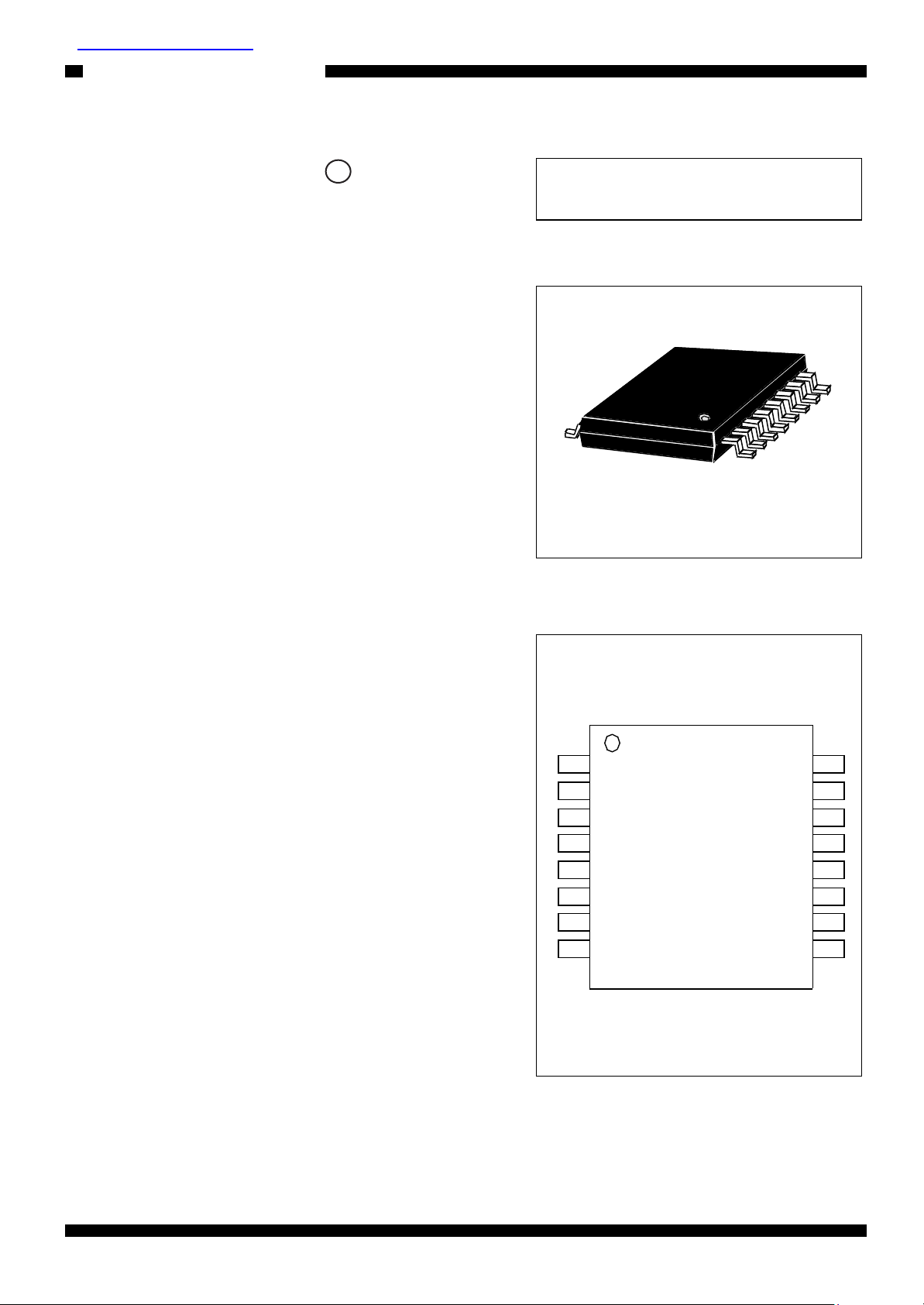
16PIN SVMFP
Features
- Manufactured by SMOS5AP process technology
- Built in 2 Channel Circuit of H-Bridge Driver
- 4 Mode Drive(Forward, Reverse, Brake, Open)
- Direct Interface from the MCU
- Low ON-Resistance Ron=0.8 ohm(typ)
Freescale Semicond
- Dual Channel Parallel Drive (Ron=0.8 ohm:typ)
- IDR=0.7A (Cont.)
- Low Consumption Power
- Built in Shoot Through Current Prevention Circuit
- Built in Low Voltage Shutdown Circuit
- PWM Control frequency 200kHz(Max.)
- Comes in 16-pin Very Fine Mini-flat Package
(pin pitch : 0.65mm)
1
2
3
4
5
6
7
8
Pin Connections
OUT1A
VM1
IN1A
IN1B
VC
OEB
LGND
OUT1B
MPC17533
(Top View)
PGND2
OUT2A
IN2A
IN2B
VG
VM2
OUT2B
PGND1
16
15
14
13
12
11
10
9
*SMARTMOS is a registered trademark of Motorola Inc.
*Specifications in this data sheet may be changed without prior notice.
For More Information On This Product,
Go to: www.freescale.com
1
MPC17533 :MAR.19. 2002 REV.0.4
Page 2
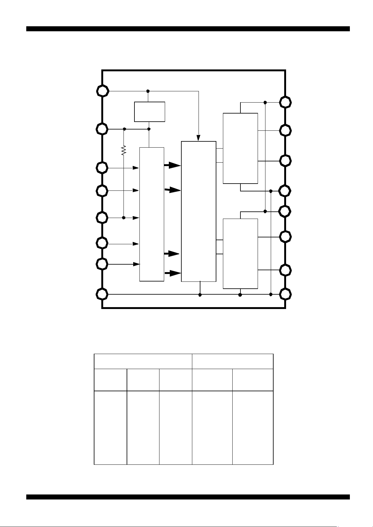
Block Diagram
..
nc.
VG
VC
IN1A
12
5
3
Freescale Semiconductor, Inc.
Low voltage
Detector
H
Bridge
1
2
1
8
VM1
OUT1A
OUT1B
uctor, I
Function Table
Freescale Semicond
IN1B
OEB
IN2A
IN2B
LGND
4
6
14
13
7
Control
Logic
Level Shifter P redriver
H
Bridge
2
Each GND pin are connected by Metal line
Input Output
9
11
15
10
16
PGND1
VM2
OUT2A
OUT2B
PGND2
OEB
IN1A
IN2A
IN1B
IN2B
OUT1A
OUT2A
L L L L L
L H
L H L
L L H L H
L H H Z Z
H X X Z Z
Pin6(OEB) is Pull-Up by internal resistance.
For More Information On This Product,
Go to: www.freescale.com
2
MPC17533 :MAR.19. 2002 REV.0.4
OUT1B
OUT2B
Z : High impedance
X : Don't care
Page 3
Freescale Semiconductor, Inc.
Maximum Ratings
Driver Circuit Power Supply Voltage
Pre-Driver Circuit Power Supply Voltage
Control Circuit Power Supply Voltage
Singnal Input Voltage
Driver Output Current (continuous)
..
Driver Output Current (pulsed) *2
nc.
uctor, I
Operating Junction Temperature
Storage Temperature Range
Thermal Resistance *3
Power Dissipation *4
*1
Rating Symbol Min. Max. Unit
VM
VG - 0.5 14.0 V
VC
VIN
IDR
IDRp
Tj
Tstg
ROja
PD 830--- mW
- 0.5 8.0
- 0.5
- 0.5 VC+0.5
---
---
- 55
--150
7.0
0.7
1.4
150
150
V
V
V
A
A
degC
degC
degC./W
*1) Device may be damaged when used over the ratings.
*2) Ta=25C, Peak time is within 10ms at intervals 0.2seconds.
*3) 37 X 50 X 1.6[mm] Glass EPOXY Board mount.
*4) Ta=25C
Recommended Operating Condition
Characteristics Symbol Min. Unit
Driver Circuit Power Supply Voltage
Freescale Semicond
Control Circuit Power Supply Voltage
Signal Input Voltage
Pulse Input Frequency
Input Pulse Rise Time
Input Pulse Fall Time
Operating Ambient Temperature
Typ.
VM
VC
VIN
FIN kHz
TR
TF
Topr
2.0
2.7
0
---
---
---
-20
5.0
5.0
---
---
---
--25
Max.
6.8
5.7
VC
200
1.0
1.0
65
V
V
V
us
us
degC
Capacitor for Charge Pump
Pre-Driver Circuit Power Supply Voltage
For More Information On This Product,
Go to: www.freescale.com
C1,C2,C3
3
0.01 1.0
VG V13.512
MPC17533 :MAR.19. 2002 REV.0.4
0.1
13
uF
Page 4
Freescale Semiconductor, Inc.
DC CHARACTERISTICS
Characteristics
Quiescent Power Supply Current
Driver Circuit Power Supply Current
Control Circuit Power Supply Current
Pre-Driver CircuitPower Supply Current
Active Power Supply Current
Control Circuit Power Supply Current
Pre-Driver Circuit Power Supply Current
Logic Input Function
High Level Input Voltage
..
nc.
uctor, I
Low Level Input Voltage
High Level Input Current
Low Level Input Current
Driver Output ON Resistance
Low Voltage Detection Circuit
Detection Voltage
(Ta=25C, VC=VM=5.0V, GND=0V)
OEB pin
Symbol
IMO
ICO
IGO
IC
IG
VIH
VIL
IIH
IIL - 1.0
IIL
RON
VCDET
Min.
---
---
---
---
--- mA
VCx0.7
---
---
---
---
1.5
Typ.
---
---
---
---
---
---
---
--- uA
---
50
0.8
Max. Unit
1.0
20
150
3.0
0.7
---
VCx0.3
1.0
---
100
1.2
2.52.0
uA
UA
UA
mA
V
V
uA
uA
ohm
V
Test
circuit
A
E
B
C
D
*4
*2
*3
*1
*6
*1) ICO includes current to the pre-driver circuit.
*2) IC includes current to the pre-driver circuit. IC:Fin100kHz. IG:Fin20kHz.
*3) 2.7V < VC < 5.7V
*4) IDR=0.7[A] source+sink
*5) When no input logic signal.
*6) Detection voltage is defined output become High-impedance when VC voltage is dropped.
When the gate voltage VG is applied from an external source, VG=7.5[V]
AC CHARACTERISTICS
Characteristics
Output Propagation Delay Time
Freescale Semicond
Low Voltage Detection Circuit
Detection time
tPLH,tPHL Timing Chart
IN1,IN2
50%
(Ta=25C, VC=VM=5.0V, GND=0V)
Symbol Min. Max. Unit
Turn-ON time
Turn-Off time us
tPLH
tPHL
tVCDET
---
---
---
Typ.
0.1
---
0.5
0.50.1
10
us
ms
tVCDET Timing Chart
50%
VC
VCDETon
50%
1.5
2.5
Test
circuit
VCDEToff
50%
C
D
OUTA,OUTB
tPLH
90%
tPHL
IM
10%
For More Information On This Product,
Go to: www.freescale.com
tVCDETon
MPC17533 :MAR.19. 2002 REV.0.44
tVCDEToff
90%
0%(<1uA)
Page 5

Pin Description
Symbol PIN No. Simplified Circuit Schematic Function
Freescale Semiconductor, Inc.
VC 5
VM1
5
2
2
Control Circuit
Power Supply Pin
Driver Power Supply
Voltage Input Pin
..
OUT1A
nc.
OUT1B
uctor, I
PGND1
VM2
OUT2A
1
8
9
11
15
1
9
11
15
8
10
Driver Output Pin
Driver Output Pin
Power GND Pin
Driver Power Supply
Voltage Input Pin
Driver Output Pin
Freescale Semicond
OUT2B
PGND2
IN1A
IN1B
IN2A
IN2B
OEB
VG
10
16
3
4
14
13
6
12
16
3
4
13
14
6
Pre-Driver Circuit
Driver Output Pin
Power GND Pin
VC
Control Signal
Input Pin
VC
Enable Control
Signal Input Pin
Power Supply Pin
LGND 7
ControlCircuit GND Pin
For More Information On This Product,
Go to: www.freescale.com
MPC17533 :MAR.19. 2002 REV.0.45
Page 6

Test Circuit
Freescale Semiconductor, Inc.
5V
5V
A
A
ICO IMO
VM
VC
MPC17533
IN1A
IN1B
IN2A
IN2B
OEB
IGO
13V
A
VG
..
OUT1A
OUT1B
nc.
OUT2A
OUT2B
PGND/LGND
uctor, I
Test Circuit A
13V
5V 5V
VG
VC VM
MPC17533
PGND/LGND
Test Circuit B
IN1A
IN1B
IN2A
IN2B
OEB
OUT1A
OUT1B
OUT2A
OUT2B
IIN
A
VIN
V
Freescale Semicond
5V
13V
VG
VC VM
MPC17533
PGND/LGND
5V
IN1A
IN1B
IN2A
IN2B
OEB
R=8 [ohm]
OUT1A
OUT1B
OUT2A
OUT2B
R=8 [ohm]
Test Circuit C
For More Information On This Product,
Go to: www.freescale.com
MPC17533 :MAR.19. 2002 REV.0.46
Page 7

Test Circuit
Freescale Semiconductor, Inc.
13V
VG
VC VM
..
MPC17533
nc.
uctor, I
PGND/LGND
Test Circuit D
5V
IN1A
IN1B
IN2A
IN2B
OEB
OUT1A
OUT1B
OUT2A
OUT2B
5V
VC VM
V
5V
A
IN1A
IN1B
IN2A
IN2B
OEB
MPC17533
For IG Test
13V
A
VG
V
PGND/LGND
Test Circuit E
OUT1A
OUT1B
OUT2A
OUT2B
100kHz
Fin
Freescale Semicond
For More Information On This Product,
Go to: www.freescale.com
7
MPC17533 :MAR.19. 2002 REV.0.4
Page 8

Precautions on Application
(1)When applying the gate voltage VG from an external source, be sure to connect it via a
resistor equal to or greater than RG=VG/0.02[ohm]. However, this resistance is unnecessary
if you are connecting a charge pump output from a SMARTMOS product.
..
nc.
Freescale Semiconductor, Inc.
MPC17533
VG
C2H
C1H
C2L
C1L
VG < 14[V]
RG > VG/0.02[ohm]
CG = 0.01[uF]
OPEN
uctor, I
Freescale Semicond
(2)Switching from the state of active current loading to high-impedance mode, indactance load
and P.C.B. layout may induce over maximum ratings to a power supply pin. Zener diode or
capacitor at VM pin will protect kick back voltage(it depends on the indactance load).
The schottky diode at output pin will also protect it.
VM
OUTA
OUTB
(3)Connect a capacitor of sufficient capacitance between the power supply and ground pins.
For all large-current paths, use sufficiently wide copper conductor patterns and route them
in the shortest distance possible.
VM
OUTA
OUTB
(4)When using SMARTMOS products in your circuit design, make sure they are fully protected
against static charge.
For More Information On This Product,
Go to: www.freescale.com
8
MPC17533 :MAR.19. 2002 REV.0.4
Page 9

■ 16 ピン SVMFP 外形寸法図
SPEC
MIN TYP MAX
A ***** 1.95 2.05
A1 0.10 0.15 0.20
b
0.25 0.30 0.35
C 0.18 0.20 0.25
D ***** 5.45 MAX
D1 5.20 5.25 5.30
e 0.60 0.65 0.70
E 5.25 5.30 5.35
He 7.70 7.90 8.10
L 0.45 0.60 0.75
L1 1.20 1.30 1.40
x
***** ***** 0.12
y
0.05
Z1 0.25 0.35 0.47
θ
0.0° 4.0° 9.8°
A
Z1 e
b
x
y
L1
L
A
D
D1
H
e
E
C
A1
θ
A部拡大図
Freescale Semicond
uctor, I
nc.
..
Freescale Semiconductor, Inc.
For More Information On This Product,
Go to: www.freescale.com
Page 10

当社は、本書に記載した製品について、予告なく変更を加える権限を保有しています。
当社はここに記載した製品、回路の適用、使用に起因するいかなる責務を負うものではなく、また、当社の特許権または第三者の
権利に基づくライセンスを許諾するものでもありません。当社の製品は、外科的に人体に移植することを意図したシステムの構成
部品として、または、他の生命維持を意図した用途に、または、当社の製品の不具合により人体に危害を加えたり死に至らしめる
かもしれない状況が発生するような用途に使用するために、設計、意図または許可されているものではありません。購入者が万一
このような意図または許可されていない用途のために当社の製品を購入あるいは使用する場合、購入者は当社およびその役員、従
業者、子会社、関連会社、代理店に対し、直接または間接を問わず、当該使用に関連した傷害や死についてのすべての申し立て
(たとえ、当社が部品の設計や製造において不注意であったという主張であったとしても)から生ずるすべての請求、費用、損害、
および相当の弁護士費用を補償し、被害が及ばないようにするものとします。
SPS.TSPG.GAO
Freescale Semicond
uctor, I
nc.
..
Freescale Semiconductor, Inc.
For More Information On This Product,
Go to: www.freescale.com
 Loading...