

Page 1
O
CO
O
S
G
Freescale Semiconductor
Technical Data
Heterojunction Bipolar Transistor
Technology (InGaP HBT)
Broadband High Linearity Amplifier
N
The MMG3003NT1 is a General Purpose Amplifier that is internally
input matched and internally output prematched. It is designed for a broad
range of Class A, small- signal, high linearity, general purpose applica-
I
tions. It is suitable for applications with frequencies from 40 to 3600 MHz
such as Cellular, PCS, BWA, WLL, PHS, CATV, VHF, UHF, UMTS and
general small - signal RF.
Features
• Frequency: 40-3600 MHz
• P1dB: 24 dBm @ 900 MHz
• Small-Signal Gain: 20 dB @ 900 MHz
• Third Order Output Intercept Point: 40.5 dBm @ 900 MHz
• Single Voltage Supply
• Internally Matched to 50 Ohms
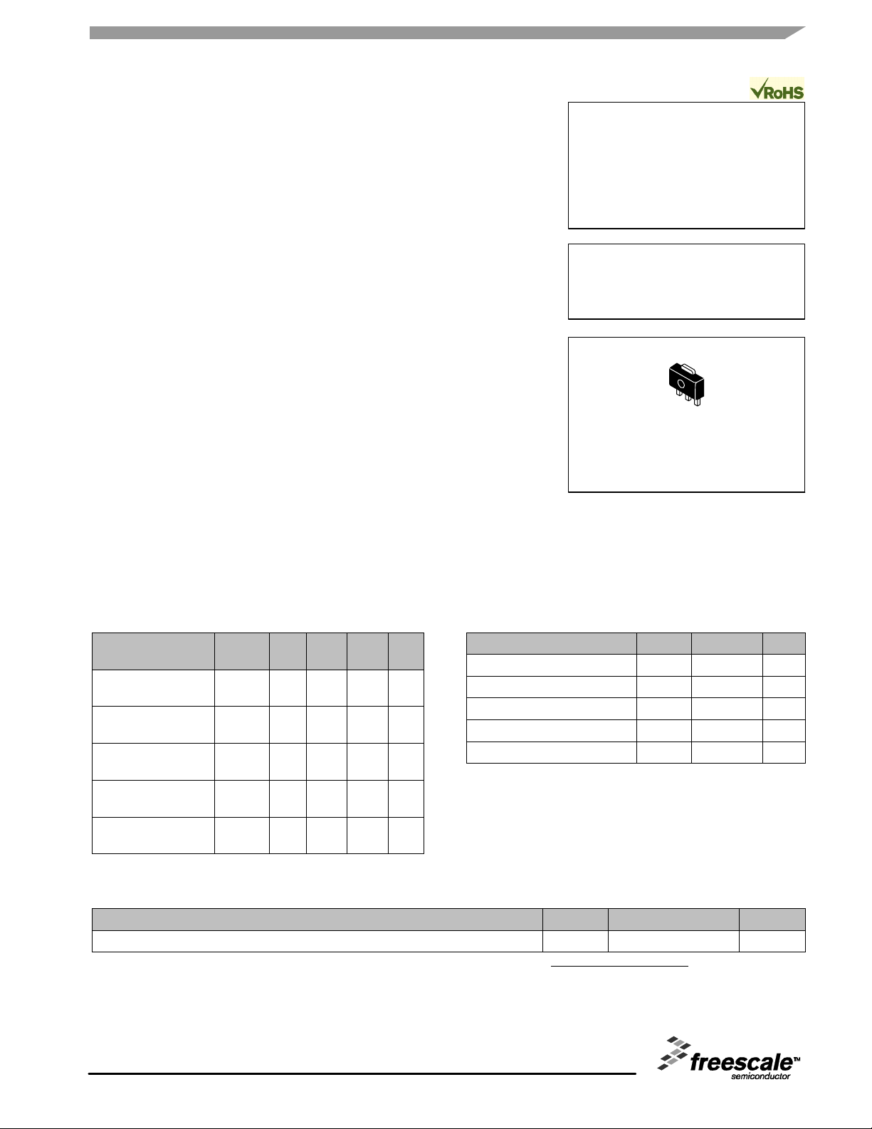
• Low Cost SOT-89 Surface Mount Package
• RoHS Compliant
• In Tape and Reel. T1 Suffix = 1000 Units per 12 mm, 7 inch Reel.
R NEW DE
Document Number: MMG3003NT1
Rev. 7, 3/2008
MMG3003NT1
40-3600 MHz, 20 dB
24 dBm
InGaP HBT
1
2
3
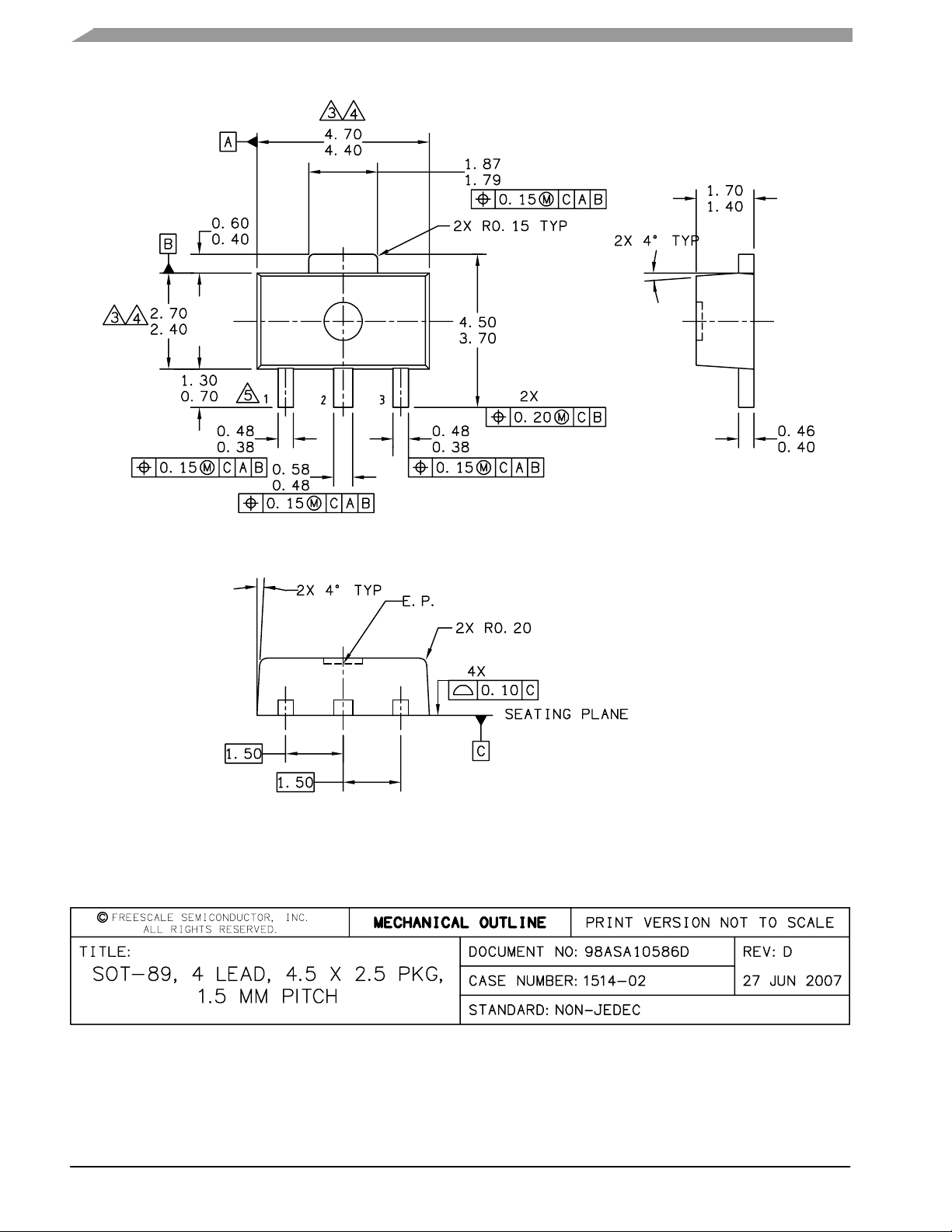
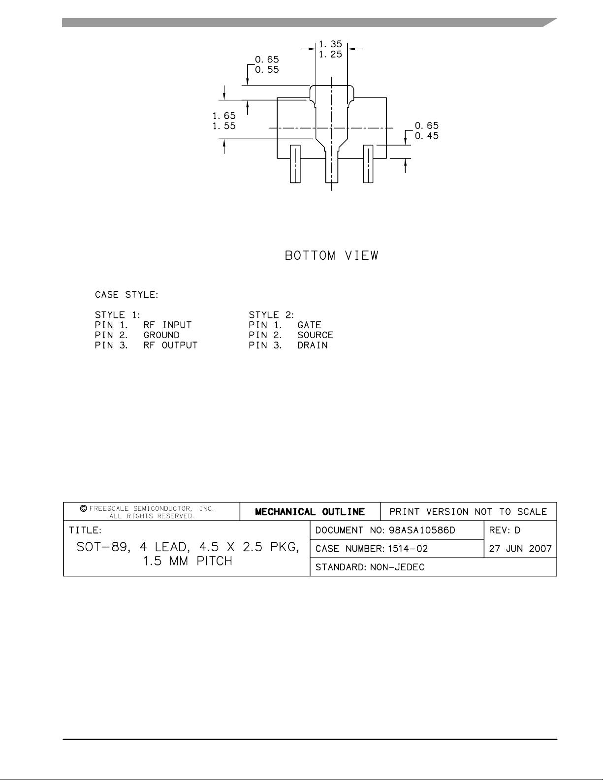
CASE 1514-02, STYLE 1
SOT-89
PLASTIC
Table 1. Typical Performance
Characteristic Symbol 900
Small -Signal Gain
(S21)
Input Return Loss
(S11)
MMENDED F
Output Return Loss
(S22)
Power Output @1dB
Compression
Third Order Output
Intercept Point
1. V
= 6.2 Vdc, TC = 25°C, 50 ohm system
CC
ORL -9.3 −14.5 - 10.2 dB
P1db 24 23.3 20.5 dBm
(1)
2140
3500
MHz
MHz
G
IRL -15 -14.1 -11.2 dB
IP3 40.5 40 37 dBm
20 16.9 12 dB
p
Unit
MHz
Table 2. Maximum Ratings
Rating Symbol Value Unit
Supply Voltage V
Supply Current I
RF Input Power P
Storage Temperature Range T
Junction Temperature
2. For reliable operation, the junction temperature should not
exceed 150°C.
(2)
T RE
Table 3. Thermal Characteristics (V
Thermal Resistance, Junction to Case R
N
3. Refer to AN1955, Thermal Measurement Methodology of RF Power Amplifiers. Go to http://www.freescale.com/rf.
Select Documentation/Application Notes - AN1955.
= 6.2 Vdc, ICC = 180 mA, TC = 25°C)
CC
Characteristic Symbol Value
θ
JC
CC
CC
in
stg
T
J
31.6 °C/W
7 V
400 mA
15 dBm
-65 to +150 °C
150 °C
(3)
Unit
NOT RECOMMENDED FOR NEW DESIGN
Freescale Semiconductor, Inc., 2004- 2008. All rights reserved.
RF Device Data
Freescale Semiconductor
MMG3003NT1
1
Page 2
O
CO
O
S
G
Table 4. Electrical Characteristics (V
Small -Signal Gain (S21) G
Input Return Loss (S11) IRL — -15 — dB
Output Return Loss (S22) ORL — -9.3 — dB
Power Output @ 1dB Compression P1dB — 24 — dBm
N
Third Order Output Intercept Point IP3 — 40.5 — dBm
Noise Figure NF — 4 — dB
I
Supply Current
Supply Voltage
1. For reliable operation, the junction temperature should not exceed 150°C.
(1)
(1)
R NEW DE
= 6.2 Vdc, 900 MHz, TC = 25°C, 50 ohm system, in Freescale Application Circuit)
CC
Characteristic Symbol Min Typ Max Unit
p
I
CC
V
CC
19.3 20 — dB
160 180 205 mA
— 6.2 — V
MMENDED F
T RE
N
MMG3003NT1
2
NOT RECOMMENDED FOR NEW DESIGN
RF Device Data
Freescale Semiconductor
Page 3
O
CO
O
S
G
N
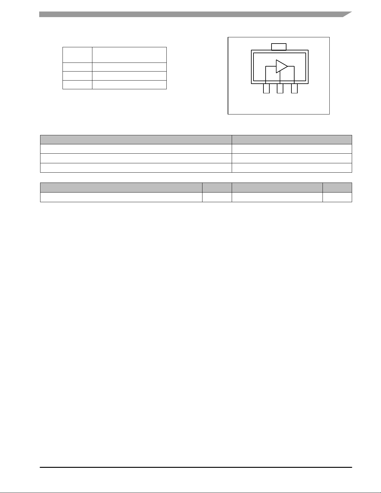
Table 5. Functional Pin Description
Pin
Number
1 RF
2 Ground
3 RF
Pin Function
in
/DC Supply
out
2
1
32
I
Table 6. ESD Protection Characteristics
Test Conditions/Test Methodology Class
Human Body Model (per JESD 22-A114) 1B (Minimum)
Machine Model (per EIA/JESD 22-A115) A (Minimum)
Charge Device Model (per JESD 22-C101) IV (Minimum)
Table 7. Moisture Sensitivity Level
Test Methodology Rating Package Peak Temperature Unit
Per JESD 22-A113, IPC/JEDEC J - STD-020 1 260 °C
R NEW DE
Figure 1. Functional Diagram
MMENDED F
T RE
N
RF Device Data
Freescale Semiconductor
NOT RECOMMENDED FOR NEW DESIGN
MMG3003NT1
3
Page 4
O
CO
O
S
G
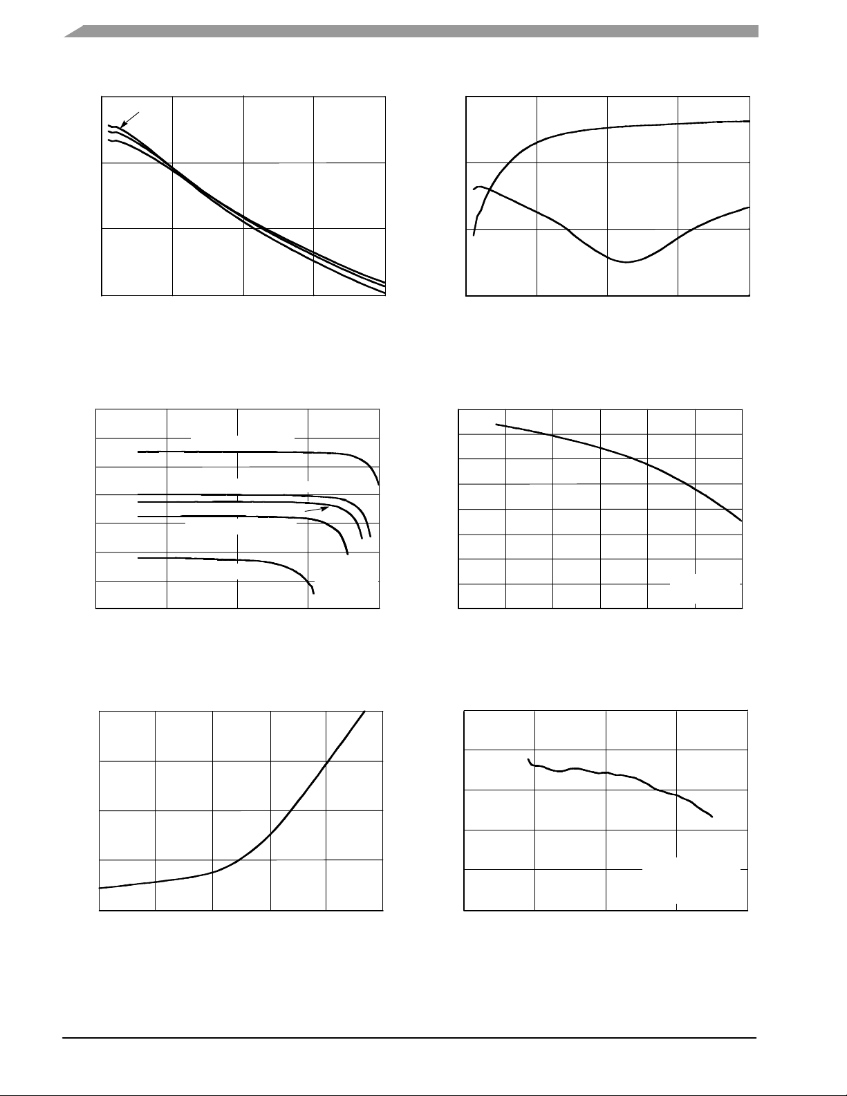
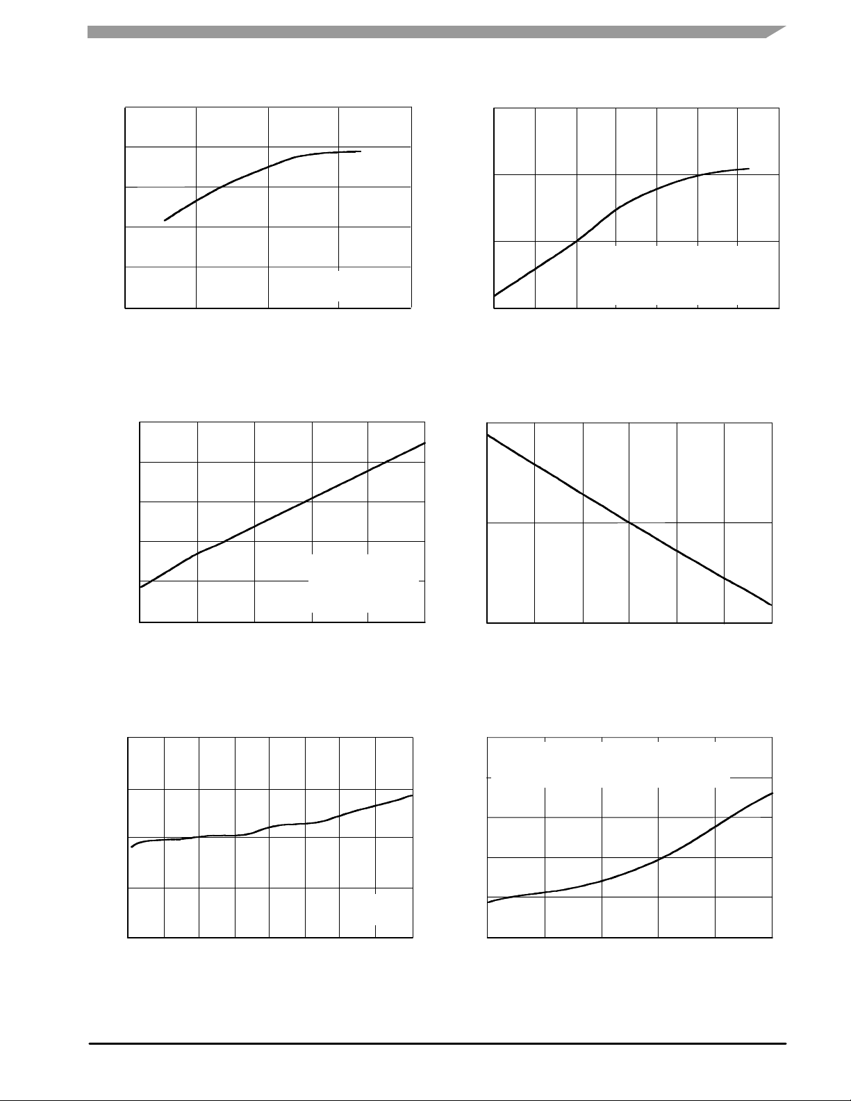
50 OHM TYPICAL CHARACTERISTICS
25
TC = 85°C
25°C
−40°C
20
N
15
I
, SMALL−SIGNAL GAIN (dB)
p
G
VCC = 6.2 Vdc
10
0
Figure 2. Small-Signal Gain (S21) versus
1234
23
21
R NEW DE
19
17
15
13
, SMALL−SIGNAL GAIN (dB)
p
G
11
9
5
Figure 4. Small-Signal Gain versus Output
3500 MHz, C5 = 0.5 pF
10 15 20
P
out
f, FREQUENCY (GHz)
Frequency
900 MHz, C5 = 2.7 pF
1960 MHz, C5, C6 = 1.3 pF
2140 MHz, C5, C6 = 1.3 pF
2600 MHz, C5 = 1.2 pF
, OUTPUT POWER (dBm)
Power
VCC = 6.2 Vdc
ICC = 180 mA
0
S22
−10
S11, S22(dB)
−20
S11
−30
0
Figure 3. Input/Output Return Loss versus
25
24
23
22
21
20
19
18
P1dB, 1 dB COMPRESSION POINT (dBm)
17
25
12 3
f, FREQUENCY (GHz)
Frequency
f, FREQUENCY (GHz)
Figure 5. P1dB versus Frequency
VCC = 6.2 Vdc
ICC = 180 mA
4
VCC =6.2 Vdc
ICC = 180 mA
3.532.521.510.5
200
MMENDED F
150
100
T RE
50
, COLLECTOR CURRENT (mA)
CC
I
0
N
4
Figure 6. Collector Current versus Collector
MMG3003NT1
4
4.5 5 5.5
VCC, COLLECTOR VOLTAGE (V)
Voltage
45
42
39
36
33
30
6
6.5
0
IP3, THIRD ORDER OUTPUT INTERCEPT POINT (dBm)
Figure 7. Third Order Output Intercept Point
123
f, FREQUENCY (GHz)
versus Frequency
VCC = 6.2 Vdc
ICC = 180 mA
100 kHz Tone Spacing
4
RF Device Data
Freescale Semiconductor
NOT RECOMMENDED FOR NEW DESIGN
Page 5
O
CO
O
S
G
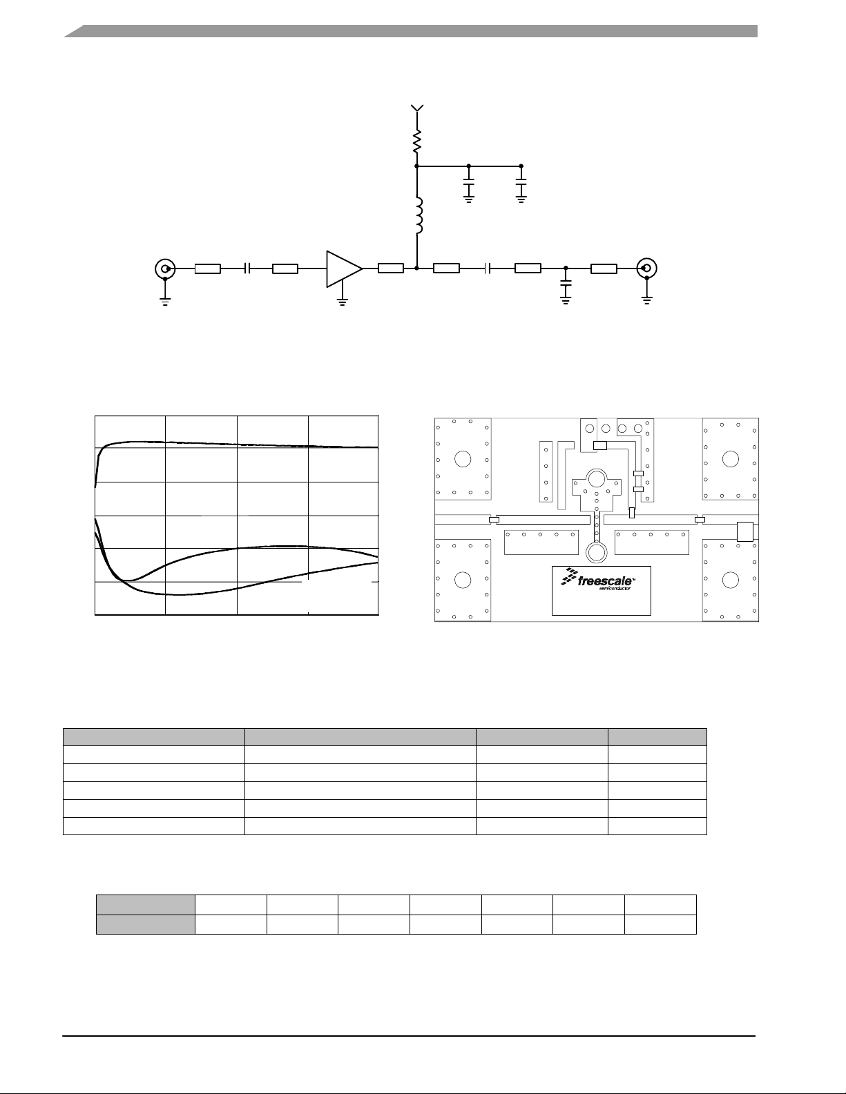
50 OHM TYPICAL CHARACTERISTICS
45
42
39
N
36
I
33
30
5.8
IP3, THIRD ORDER OUTPUT INTERCEPT POINT (dBm)
Figure 8. Third Order Output Intercept Point
−30
6
VCC, COLLECTOR VOLTAGE (V)
versus Collector Voltage
f = 900 MHz
100 kHz Tone Spacing
6.2 6.4 6.6
R NEW DE
−40
−50
−60
IMD, THIRD ORDER
−70
INTERMODULATION DISTORTION (dBc)
−80
P
, OUTPUT POWER (dBm)
out
Figure 10. Third Order Intermodulation versus
Output Power
MMENDED F
8
6
VCC = 6.2 Vdc
ICC = 180 mA
f = 900 MHz
100 kHz Tone Spacing
24912151821
42
41
40
39
IP3, THIRD ORDER OUTPUT INTERCEPT POINT (dBm)
Figure 9. Third Order Output Intercept Point
5
10
4
10
MTTF (YEARS)
3
10
120
−20
−30
125 130 135 140 145
NOTE: The MTTF is calculated with VCC = 6.2 Vdc, ICC = 180 mA
Figure 11. MTTF versus Junction Temperature
VCC = 6.2 Vdc, ICC = 180 mA, f = 2140 MHz, C5 = 1.3 pF
Single−Carrier W−CDMA, 3.84 MHz Channel Bandwidth
Input Signal PAR = 8.5 dB @ 0.01% Probability (CCDF)
VCC = 6.2 Vdc
f = 900 MHz
100 kHz Tone Spacing
8 Vdc Supply with 10 W Dropping Resistor
T, TEMPERATURE (_C)
versus Case Temperature
TJ, JUNCTION TEMPERATURE (°C)
100−40 −20 0 20 40 60 80
150
4
T RE
NF, NOISE FIGURE (dB)
2
N
0
0
0.5 2 3
Figure 12. Noise Figure versus Frequency
RF Device Data
Freescale Semiconductor
VCC = 6.2 Vdc
ICC = 180 mA
1 1.5 2.5 3.5
f, FREQUENCY (GHz)
−40
−50
−60
NOT RECOMMENDED FOR NEW DESIGN
−70
4
ACPR, ADJACENT CHANNEL POWER RATIO (dBc)
9
P
, OUTPUT POWER (dBm)
out
Figure 13. Single-Carrier W-CDMA Adjacent
Channel Power Ratio versus Output Power
17151311
MMG3003NT1
19
5
Page 6
O
CO
O
S
G
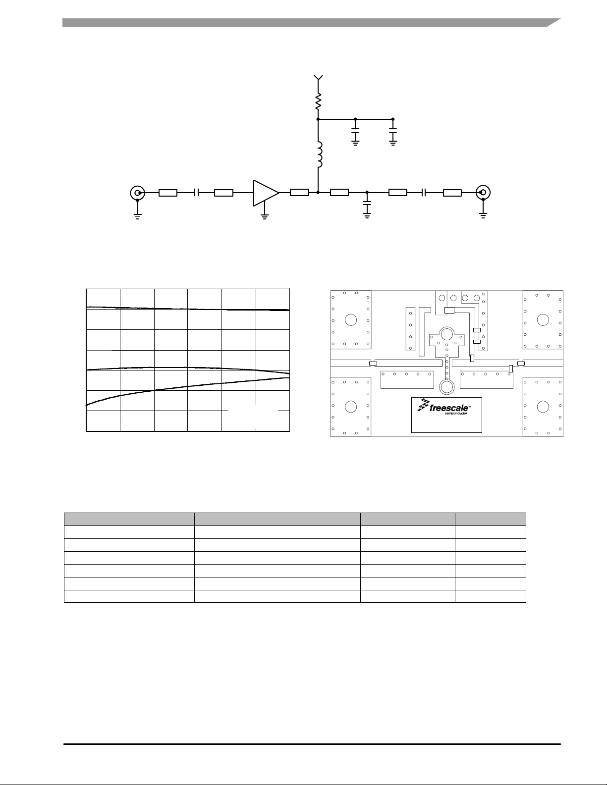
50 OHM APPLICATION CIRCUIT: 40-800 MHz
V
SUPPLY
R1
N
I
RF
INPUT
Z1 0.347″ x 0.058″ Microstrip
Z2 0.575″ x 0.058″ Microstrip
Z3 0.172″ x 0.058″ Microstrip
Z4 0.403″ x 0.058″ Microstrip
30
R NEW DE
20
10
0
−10
S21, S11, S22 (dB)
Z1 Z2
C1
S21
S22
C3 C4
L1
DUT
V
CC
Figure 14. 50 Ohm Test Circuit Schematic
Z4Z3
C2
Z5 0.286″ x 0.058″ Microstrip
Z6 0.061″ x 0.058″ Microstrip
PCB Getek Grade ML200C, 0.031″, εr = 4.1
C1
RF
Z5
C5
OUTPUT
Z6
R1
C4
C3
L1
C2
C5
−20
−30
0
200 400 600
Figure 15. S21, S11 and S22 versus Frequency
MMENDED F
Table 8. 50 Ohm Test Circuit Component Designations and Values
Part Description Part Number Manufacturer
C1, C2, C4 0.01 µF Chip Capacitors C0603C103J5RAC Kemet
C3 68 pF Chip Capacitor C0805C680J5RAC Kemet
(1)
C5
L1 470 nH Chip Inductor BK2125HM471-T Taiyo Yuden
R1
1. Tuning capacitor: Capacitor value and location on the transmission line are varied for different frequencies.
S11
f, FREQUENCY (MHz)
2.7 pF Chip Capacitor 12105J2R7BS AVX
7.5 W Chip Resistor
VCC = 6.2 Vdc
ICC = 180 mA
800
MMG30XX
Rev 2
Figure 16. 50 Ohm Test Circuit Component Layout
RK73B2ATTE7R5J KOA Speer
T RE
Table 9. Supply Voltage versus R1 Values
N
Supply Voltage 7 8 9 10 11 12 V
R1 Value 4.4 10 15.6 21 27 32 Ω
Note: To provide VCC = 6.2 Vdc and ICC = 180 mA at the device.
NOT RECOMMENDED FOR NEW DESIGN
MMG3003NT1
6
RF Device Data
Freescale Semiconductor
Page 7
O
CO
O
S
G
50 OHM APPLICATION CIRCUIT: 800-1100 MHz
V
SUPPLY
R1
N
I
30
20
RF
INPUT
Z1 Z2
Z1, Z6 0.347″ x 0.058″ Microstrip
Z2 0.575″ x 0.058″ Microstrip
Z3 0.172″ x 0.058″ Microstrip
S21
R NEW DE
10
0
−10
S21, S11, S22 (dB)
−20
−30
−40
Figure 18. S21, S11 and S22 versus Frequency
S22
S11
f, FREQUENCY (MHz)
C1
C3 C4
L1
DUT
V
CC
Figure 17. 50 Ohm Test Circuit Schematic
VCC = 6.2 Vdc
ICC = 180 mA
1100600 700 800 900 1000
1200
Z4Z3
C5
Z4 0.333″ x 0.058″ Microstrip
Z5 0.07″ x 0.058″ Microstrip
PCB Getek Grade ML200C, 0.031″, εr = 4.1
C1
Figure 19. 50 Ohm Test Circuit Component Layout
RF
OUTPUT
C2
MMG30XX
Rev 2
Z6
R1
C4
C3
L1
C2
C5
Z5
Table 10. 50 Ohm Test Circuit Component Designations and Values
MMENDED F
C1, C2 47 pF Chip Capacitors C0805C470J5RAC Kemet
C3 68 pF Chip Capacitor C0805C680J5RAC Kemet
C4 0.01 µF Chip Capacitor C0603C103J5RAC Kemet
(1)
C5
L1 22 nH Chip Inductor HK160822NJ-T Taiyo Yuden
R1
1. Tuning capacitor: Capacitor value and location on the transmission line are varied for different frequencies.
T RE
Part Description Part Number Manufacturer
2.7 pF Chip Capacitor 06035J2R7BS AVX
7.5 W Chip Resistor
RK73B2ATTE7R5J KOA Speer
N
RF Device Data
Freescale Semiconductor
NOT RECOMMENDED FOR NEW DESIGN
MMG3003NT1
7
Page 8

O
CO
O
S
G
50 OHM APPLICATION CIRCUIT: 1800-2400 MHz
V
SUPPLY
R1
N
I
RF
INPUT
Z1 Z2
Z1, Z7 0.347″ x 0.058″ Microstrip
Z2 0.575″ x 0.058″ Microstrip
Z3 0.172″ x 0.058″ Microstrip
Z4 0.047″ x 0.058″ Microstrip
30
R NEW DE
20
10
0
−10
S21, S11, S22 (dB)
−20
−30
−40
1600
Figure 21. S21, S11 and S22 versus Frequency
1800 2000 2200 2400
f, FREQUENCY (MHz)
C1
S21
S22
S11
C3 C4
L1
DUT
V
CC
Figure 20. 50 Ohm Test Circuit Schematic
VCC = 6.2 Vdc
ICC = 180 mA
2600
Z4Z3
Z5 0.062″ x 0.058″ Microstrip
Z6 0.466″ x 0.058″ Microstrip
PCB Getek Grade ML200C, 0.031″, εr = 4.1
Z5
C5
C1
Figure 22. 50 Ohm Test Circuit Component Layout
C6
Z6
MMG30XX
Rev 2
R1
C2
C5
RF
OUTPUT
Z7
C4
C3
L1
C6
C2
MMENDED F
Table 11. 50 Ohm Test Circuit Component Designations and Values
Part Description Part Number Manufacturer
C1, C2 47 pF Chip Capacitors C0805C470J5RAC Kemet
C3 68 pF Chip Capacitor C0805C680J5RAC Kemet
C4 0.01 µF Chip Capacitor C0603C103J5RAC Kemet
(1)
C5
(1)
C6
L1 22 nH Chip Inductor HK160822NJ-T Taiyo Yuden
T RE
R1
1. Tuning capacitor: Capacitor value and location on the transmission line are varied for different frequencies.
1.2 pF Chip Capacitor 06035J1R2BS AVX
0.1 pF Chip Capacitor 06035J0R1BS AVX
7.5 W Chip Resistor
RK73B2ATTE7R5J KOA Speer
N
MMG3003NT1
8
NOT RECOMMENDED FOR NEW DESIGN
RF Device Data
Freescale Semiconductor
Page 9

O
CO
O
S
G
50 OHM APPLICATION CIRCUIT: 2500-2700 MHz
V
SUPPLY
R1
N
I
30
20
RF
INPUT
Z1 Z2
Z1, Z6 0.347″ x 0.058″ Microstrip
Z2 0.575″ x 0.058″ Microstrip
Z3 0.086″ x 0.058″ Microstrip
S21
R NEW DE
10
0
−10
S21, S11, S22 (dB)
−20
−30
−40
2200
2300 2400 2600 2700
Figure 24. S21, S11 and S22 versus Frequency
S22
S11
2500
f, FREQUENCY (MHz)
C1
L1
DUT
V
CC
Figure 23. 50 Ohm Test Circuit Schematic
VCC = 6.2 Vdc
ICC = 180 mA
2800
Z4Z3
C5
Z4 0.085″ x 0.058″ Microstrip
Z5 0.404″ x 0.058″ Microstrip
PCB Getek Grade ML200C, 0.031″, εr = 4.1
C1
Figure 25. 50 Ohm Test Circuit Component Layout
Z5
C3 C4
Z6
C2
R1
MMG30XX
Rev 2
RF
OUTPUT
C4
C3
L1
C2
C5
Table 12. 50 Ohm Test Circuit Component Designations and Values
MMENDED F
C1, C2 2.2 pF Chip Capacitors 06035J2R2BS AVX
C3 68 pF Chip Capacitor C0805C680J5RAC Kemet
C4 0.01 µF Chip Capacitor C0603C103J5RAC Kemet
(1)
C5
L1 39 nH Chip Inductor HK160839NJ-T Taiyo Yuden
R1
1. Tuning capacitor: Capacitor value and location on the transmission line are varied for different frequencies.
T RE
Part Description Part Number Manufacturer
1.2 pF Chip Capacitor 06035J1R2BS AVX
7.5 W Chip Resistor
RK73B2ATTE7R5J KOA Speer
N
RF Device Data
Freescale Semiconductor
NOT RECOMMENDED FOR NEW DESIGN
MMG3003NT1
9
Page 10

O
CO
O
S
G
50 OHM APPLICATION CIRCUIT: 3400-3600 MHz
V
SUPPLY
R1
N
I
RF
INPUT
Z1, Z6 0.347″ x 0.058″ Microstrip
Z2 0.575″ x 0.058″ Microstrip
Z3 0.086″ x 0.058″ Microstrip
20
R NEW DE
15
10
5
0
−5
S21, S11, S22 (dB)
−10
−15
−20
3200
3300 3400 3600 3700
Figure 27. S21, S11 and S22 versus Frequency
Z1 Z2
C1
S21
S22
S11
3500
f, FREQUENCY (MHz)
L1
DUT
V
CC
Figure 26. 50 OhmTest Circuit Schematic
VCC = 6.2 Vdc
ICC = 180 mA
3800
Z4Z3
C5
Z4 0.085″ x 0.058″ Microstrip
Z5 0.404″ x 0.058″ Microstrip
PCB Getek Grade ML200C, 0.031″, εr = 4.1
Figure 28. 50 Ohm Test Circuit Component Layout
Z5
C1
C3 C4
Z6
C2
R1
MMG30XX
Rev 2
RF
OUTPUT
C4
C3
L1
C2
C5
MMENDED F
Table 13. 50 OhmTest Circuit Component Designations and Values
Part Description Part Number Manufacturer
C1, C2 2.2 pF Chip Capacitors 06035J2R2BS AVX
C3 68 pF Chip Capacitor C0805C680J5RAC Kemet
C4 0.01 µF Chip Capacitor C0603C103J5RAC Kemet
(1)
C5
L1 39 nH Chip Inductor HK160839NJ-T Taiyo Yuden
R1
T RE
1. Tuning capacitor: Capacitor value and location on the transmission line are varied for different frequencies.
0.5 pF Chip Capacitor 06035J0R5BS AVX
7.5 W Chip Resistor
RK73B2ATTE7R5J KOA Speer
N
MMG3003NT1
10
NOT RECOMMENDED FOR NEW DESIGN
RF Device Data
Freescale Semiconductor
Page 11
O
CO
O
S
G
50 OHM TYPICAL CHARACTERISTICS
f
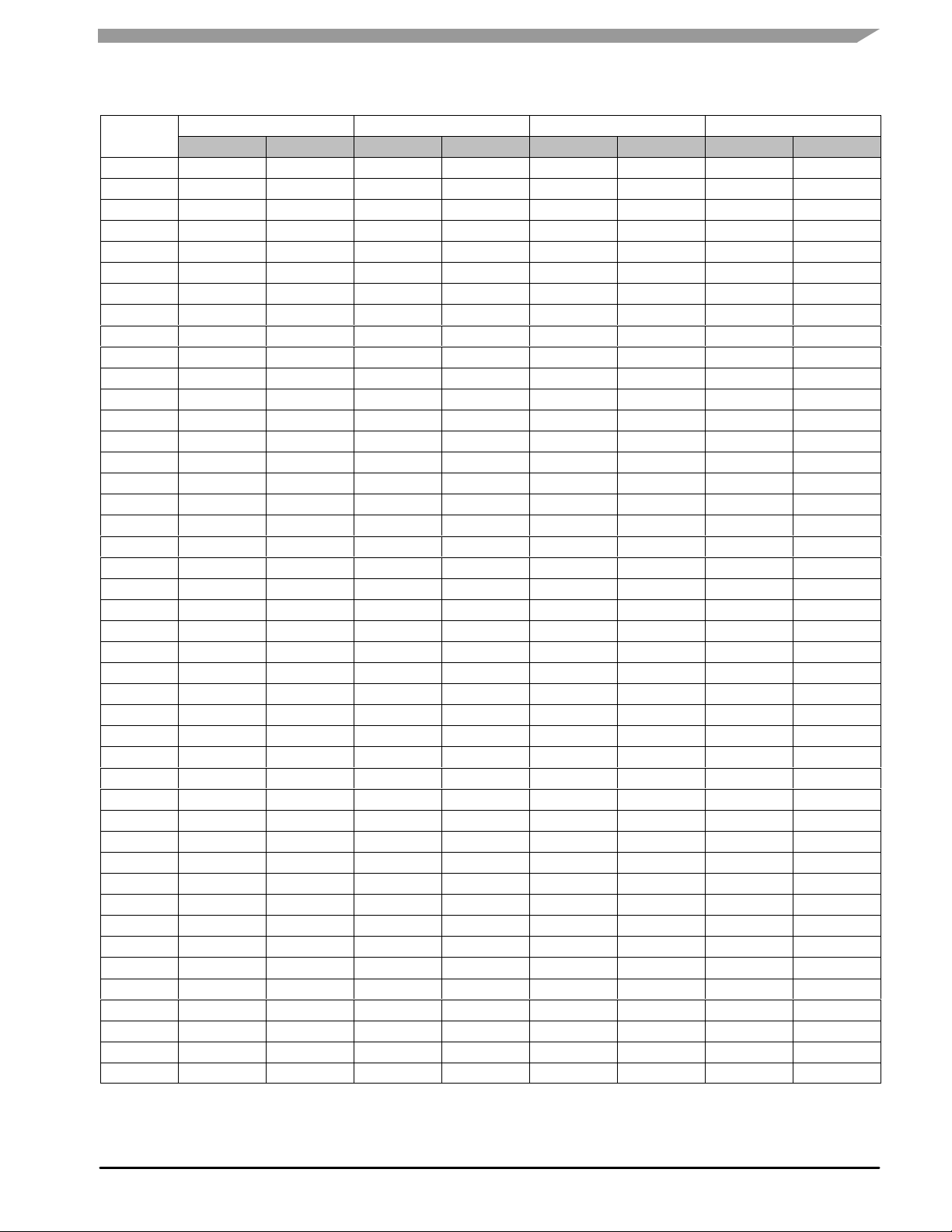
Table 14. Common Emitter S - Parameters (V
S
11
MHz
0100 0.141 178.297 12.985 173.850 0 0.057 0.785 0 0.087 - 167.704
0150 0.153 175.556 12.654 168.9 0.057 - 0.913 0.136 - 137.479
0200 0.155 160.177 13.067 164.046 0.059 - 2.423 0.125 - 131.397
N
0250 0.152 159.068 12.851 160.334 0.058 - 2.897 0.159 - 130.233
0300 0.147 156.309 12.685 156.518 0.058 - 3.227 0.187 - 128.649
I
0350 0.139 153.853 12.519 152.664 0.058 - 3.971 0.212 - 128.651
0400 0.135 150.838 12.327 149.087 0.057 - 4.471 0.239 - 129.263
0450 0.129 148.378 12.124 145.521 0.057 - 4.799 0.263 - 130.237
0500 0.123 145.160 11.915 142.009 0.057 - 5.285 0.285 -131.637
0550 0.117 142.332 11.694 138.634 0.057 - 5.623 0.306 -133.294
0600 0.112 139.364 11.470 135.366 0.057 - 6.012 0.326 -135.284
0650 0.106 136.769 11.238 132.093 0.057 - 6.295 0.345 -137.146
0700 0.101 133.592 11.004 128.948 0.057 - 6.705 0.362 -139.07
0750 0.096 131.187 10.770 125.882 0.057 - 7.044 0.378 - 141.171
0800 0.090 128.979 10.532 122.88 0.056 -7.277 0.394 - 143.273
0850 0.086 126.711 10.298 119.942 0.056 - 7.495 0.408 - 145.372
R NEW DE
0900 0.081 124.541 10.066 117.117 0.056 -7.847 0.422 - 147.618
0950 0.076 122.189 9.841 114.276 0.056 - 8.05 0.435 -149.849
1000 0.073 121.191 9.611 111.625 0.056 -8.311 0.447 - 151.947
1050 0.069 119.451 9.393 108.992 0.056 - 8.582 0.458 - 154.142
1100 0.065 118.827 9.170 106.412 0.056 - 8.89 0.470 - 156.289
1150 0.062 118.851 8.957 103.879 0.056 -9.079 0.480 - 158.481
1200 0.059 118.882 8.742 101.417 0.056 - 9.405 0.490 - 160.544
1250 0.056 119.703 8.541 99.039 0.056 -9.615 0.498 - 162.608
1300 0.054 120.919 8.340 96.664 0.056 -9.805 0.507 - 164.561
1350 0.051 123.223 8.143 94.364 0.056 - 10.198 0.515 - 166.501
1400 0.048 125.019 7.957 92.107 0.056 - 10.536 0.522 - 168.351
1450 0.046 128.063 7.774 89.892 0.056 - 10.724 0.530 - 170.229
1500 0.033 135.869 7.640 87.599 0.057 - 11.197 0.529 - 172.918
1550 0.030 139.127 7.475 85.482 0.057 - 11.434 0.536 - 174.487
1600 0.027 142.585 7.322 83.442 0.057 - 11.649 0.541 - 175.93
MMENDED F
1650 0.024 146.640 7.170 81.444 0.057 - 11.993 0.546 - 177.394
1700 0.023 152.580 7.040 79.397 0.058 - 12.335 0.552 - 179.018
1750 0.021 158.266 6.890 77.439 0.058 - 12.616 0.555 179.899
1800 0.021 166.196 6.756 75.477 0.058 - 12.879 0.560 178.582
1850 0.022 171.633 6.621 73.576 0.058 -13.16 0.563 177.318
1900 0.023 177.431 6.495 71.695 0.058 - 13.445 0.566 176.139
1950 0.025 -176.142 6.371 69.952 0.059 - 13.806 0.570 175.08
T RE
2000 0.027 -173.137 6.251 67.988 0.059 - 14.176 0.573 173.812
2050 0.029 -170.367 6.135 66.175 0.059 - 14.413 0.577 172.704
2100 0.031 -168.467 6.025 64.385 0.060 - 14.882 0.580 171.566
N
2150 0.033 -168.388 5.921 62.595 0.060 - 15.338 0.583 170.426
2200 0.036 -169.515 5.815 60.823 0.060 - 15.659 0.586 169.283
2250 0.039 -170.197 5.716 59.079 0.061 - 16.136 0.589 168.164
|S11| ∠φ |S21| ∠φ |S12| ∠φ |S22| ∠φ
= 6.2 Vdc, ICC = 180 mA, TC = 25°C, 50 Ohm System)
CC
S
21
S
12
S
22
NOT RECOMMENDED FOR NEW DESIGN
RF Device Data
Freescale Semiconductor
(continued)
MMG3003NT1
11
Page 12

O
CO
O
S
G
50 OHM TYPICAL CHARACTERISTICS
f
Table 14. Common Emitter S - Parameters (V
S
11
MHz
2300 0.042 -171.944 5.618 57.331 0.061 - 16.513 0.591 167.003
2350 0.045 -173.747 5.525 55.573 0.061 -16.98 0.593 165.803
N
2400 0.048 -175.268 5.431 53.848 0.062 - 17.435 0.595 164.669
2450 0.052 -177.409 5.345 52.136 0.062 - 17.955 0.597 163.447
2500 0.056 -178.703 5.258 50.405 0.062 - 18.404 0.598 162.182
I
2550 0.060 179.650 5.173 48.736 0.063 - 19.004 0.600 160.854
2600 0.063 177.705 5.096 47.012 0.063 - 19.505 0.602 159.516
2650 0.067 175.894 5.015 45.266 0.063 - 20.1 0.603 158.1
2700 0.071 174.932 4.938 43.452 0.064 -20.75 0.605 156.649
2750 0.074 172.453 4.861 41.831 0.064 - 21.297 0.607 155.174
2800 0.079 170.595 4.788 40.113 0.065 - 21.999 0.609 153.675
2850 0.083 168.962 4.715 38.402 0.065 - 22.577 0.610 152.104
2900 0.087 167.373 4.643 36.711 0.065 - 23.239 0.612 150.539
2950 0.091 165.543 4.573 35.036 0.066 - 23.942 0.614 148.941
3000 0.095 164.513 4.506 33.356 0.066 - 24.652 0.616 147.251
3050 0.099 163.309 4.438 31.684 0.066 - 25.269 0.618 145.747
R NEW DE
3100 0.103 162.077 4.373 29.98 0.067 -26.085 0.620 144.105
3150 0.107 161.249 4.308 28.307 0.067 - 26.717 0.622 142.483
3200 0.110 160.222 4.244 26.653 0.067 - 27.483 0.624 140.894
3250 0.114 159.057 4.182 25.007 0.068 - 28.223 0.626 139.31
3300 0.117 158.018 4.121 23.381 0.068 - 29.013 0.629 137.737
3350 0.119 156.94 4.061 21.791 0.068 -29.779 0.631 136.267
3400 0.122 155.757 4.004 20.196 0.069 - 30.535 0.633 134.76
3450 0.126 154.754 3.949 18.618 0.069 -31.29 0.635 6
3500 0.12826 153.898 3.895 17.049 0.06938 -31.957 0.6367 131.951
3550 0.13168 152.875 3.84045 15.491 0.06971 - 32.814 0.6392 130.655
3600 0.13497 152.157 3.78882 13.97 0.07016 -33.474 0.64031 129.412
|S11| ∠φ |S21| ∠φ |S12| ∠φ |S22| ∠φ
= 6.2 Vdc, ICC = 180 mA, TC = 25°C, 50 Ohm System) (continued)
CC
S
21
S
12
S
22
MMENDED F
T RE
N
MMG3003NT1
12
NOT RECOMMENDED FOR NEW DESIGN
RF Device Data
Freescale Semiconductor
Page 13

O
CO
O
S
G
1.7
N
I
1.27
0.86
0.64
3.86
Recommended Solder Stencil
R NEW DE
3.48
5.33
1.27
0.58
NOTES:
1. THERMAL AND RF GROUNDING CONSIDERATIONS SHOULD BE
USED IN PCB LAYOUT DESIGN.
2. DEPENDING ON PCB DESIGN RULES, AS MANY VIAS AS
POSSIBLE SHOULD BE PLACED ON THE LANDING PATTERN.
3. IF VIAS CANNOT BE PLACED ON THE LANDING PATTERN, THEN
AS MANY VIAS AS POSSIBLE SHOULD BE PLACED AS CLOSE TO
THE LANDING PATTERN AS POSSIBLE FOR OPTIMAL THERMAL
AND RF PERFORMANCE.
4. RECOMMENDED VIA PATTERN SHOWN HAS 0.381 x 0.762 MM
PITCH.
Figure 29. Recommended Mounting Configuration
7.62
0.305 diameter
2.49
2.54
MMENDED F
T RE
N
RF Device Data
Freescale Semiconductor
NOT RECOMMENDED FOR NEW DESIGN
MMG3003NT1
13
Page 14
O
CO
O
S
G
N
I
R NEW DE
PACKAGE DIMENSIONS
MMENDED F
T RE
N
MMG3003NT1
14
NOT RECOMMENDED FOR NEW DESIGN
RF Device Data
Freescale Semiconductor
Page 15
O
CO
O
S
G
N
I
R NEW DE
MMENDED F
T RE
N
RF Device Data
Freescale Semiconductor
NOT RECOMMENDED FOR NEW DESIGN
MMG3003NT1
15
Page 16

O
CO
O
S
G
N
I
R NEW DE
MMENDED F
T RE
N
MMG3003NT1
16
NOT RECOMMENDED FOR NEW DESIGN
RF Device Data
Freescale Semiconductor
Page 17

O
CO
O
S
G
PRODUCT DOCUMENTATION
Refer to the following documents to aid your design process.
Application Notes
• AN1955: Thermal Measurement Methodology of RF Power Amplifiers
• AN3100: General Purpose Amplifier Biasing
N
I
The following table summarizes revisions to this document.
Revision Date Description
5 Mar. 2007 • Corrected and updated Part Numbers in Tables 8, 10, 11, 12, and 13, Component Designations and Values,
6 July 2007 • Replaced Case Outline 1514 - 01 with 1514-02, Issue D, p. 1, 14 - 16. Case updated to add missing
7 Mar. 2008 • Removed Footnote 2, Continuous voltage and current applied to device, from Table 2, Maximum Ratings,
R NEW DE
to RoHS compliant part numbers, p. 6-10
dimension for Pin 1 and Pin 3.
p. 1
• Corrected Fig. 13, Single - Carrier W-CDMA Adjacent Channel Power Ratio versus Output Power y - axis
(ACPR) unit of measure to dBc, p. 5
• Corrected S-Parameter table frequency column label to read “MHz” versus “GHz” and corrected
frequency values from GHz to MHz, p. 11, 12
REVISION HISTORY
MMENDED F
T RE
N
RF Device Data
Freescale Semiconductor
NOT RECOMMENDED FOR NEW DESIGN
MMG3003NT1
17
Page 18

O
CO
O
S
G
N
I
How to Reach Us:
Home Page:
www.freescale.com
Web Support:
http://www.freescale.com/support
USA/Europe or Locations Not Listed:
Freescale Semiconductor, Inc.
Technical Information Center, EL516
2100 East Elliot Road
Tempe, Arizona 85284
+1-800 - 521 -6274 or +1- 480 - 768-2130
www.freescale.com/support
R NEW DE
Europe, Middle East, and Africa:
Freescale Halbleiter Deutschland GmbH
Technical Information Center
Schatzbogen 7
81829 Muenchen, Germany
+44 1296 380 456 (English)
+46 8 52200080 (English)
+49 89 92103 559 (German)
+33 1 69 35 48 48 (French)
www.freescale.com/support
Japan:
Freescale Semiconductor Japan Ltd.
Headquarters
ARCO Tower 15F
1-8 - 1, Shimo -Meguro, Meguro- ku,
Tokyo 153 -0064
Japan
0120 191014 or +81 3 5437 9125
support.japan@freescale.com
Asia/Pacific:
Freescale Semiconductor China Ltd.
MMENDED F
Exchange Building 23F
No. 118 Jianguo Road
Chaoyang District
Beijing 100022
China
+86 010 5879 8000
support.asia@freescale.com
For Literature Requests Only:
Freescale Semiconductor Literature Distribution Center
P.O. Box 5405
Denver, Colorado 80217
T RE
1-800 - 441 -2447 or 303- 675 - 2140
Fax: 303-675 - 2150
LDCForFreescaleSemiconductor@hibbertgroup.com
Information in this document is provided solely to enable system and software
implementers to use Freescale Semiconductor products. There are no express or
implied copyright licenses granted hereunder to design or fabricate any integrated
circuits or integrated circuits based on the information in this document.
Freescale Semiconductor reserves the right to make changes without further notice to
any products herein. Freescale Semiconductor makes no warranty, representation or
guarantee regarding the suitability of its products for any particular purpose, nor does
Freescale Semiconductor assume any liability arising out of the application or use of
any product or circuit, and specifically disclaims any and all liability, including without
limitation consequential or incidental damages. “Typical” parameters that may be
provided in Freescale Semiconductor data sheets and/or specifications can and do
vary in different applications and actual performance may vary over time. All operating
parameters, including “Typicals”, must be validated for each customer application by
customer’s technical experts. Freescale Semiconductor does not convey any license
under its patent rights nor the rights of others. Freescale Semiconductor products are
not designed, intended, or authorized for use as components in systems intended for
surgical implant into the body, or other applications intended to support or sustain life,
or for any other application in which the failure of the Freescale Semiconductor product
could create a situation where personal injury or death may occur. Should Buyer
purchase or use Freescale Semiconductor products for any such unintended or
unauthorized application, Buyer shall indemnify and hold Freescale Semiconductor
and its officers, employees, subsidiaries, affiliates, and distributors harmless against all
claims, costs, damages, and expenses, and reasonable attorney fees arising out of,
directly or indirectly, any claim of personal injury or death associated with such
unintended or unauthorized use, even if such claim alleges that Freescale
Semiconductor was negligent regarding the design or manufacture of the part.
Freescalet and the Freescale logo are trademarks of Freescale Semiconductor, Inc.
All other product or service names are the property of their respective owners.
Freescale Semiconductor, Inc. 2004- 2008. All rights reserved.
N
MMG3003NT1
Document Number: MMG3003NT1
Rev. 7, 3/2008
18
NOT RECOMMENDED FOR NEW DESIGN
RF Device Data
Freescale Semiconductor
 Loading...