

Page 1
Freescale Semiconductor
Technical Data
±3g, ±11g Three Axis Low-g
Document Number: MMA7341L
Rev 0, 04/2008
Micromachined Accelerometer
The MMA7341L is a low power, low profile capacitive micromachined
accelerometer featuring signal conditioning, a 1-pole low pass filter,
temperature compensation, self test, and g-Select which allows for the
selection between 2 sensitivities. Zero-g offset and sensitivity are factory set
and require no external devices. The MMA7341L includes a Sleep Mode that
makes it ideal for handheld battery powered electronics.
Features
• 3mm x 5mm x 1.0mm LGA-14 Package
• Low Current Consumption: 400 μA
• Sleep Mode: 3 μA
• Low Voltage Operation: 2.2 V – 3.6 V
• Selectable Sensitivity (±3g, ±11g)
• Fast Turn On Time (0.5 ms Enable Response Time)
• Self Test for Freefall Detect Diagnosis
• Signal Conditioning with Low Pass Filter
• Robust Design, High Shocks Survivability
• RoHS Compliant
• Environmentally Preferred Product
• Low Cost
Typical Applications
• 3D Gaming: Tilt and Motion Sensing, Event Recorder
• HDD MP3 Player: Freefall Detection
• Laptop PC: Freefall Detection, Anti-Theft
• Cell Phone: Image Stability, Text Scroll, Motion Dialing, E-Compass
• Pedometer: Motion Sensing
• PDA: Text Scroll
• Navigation and Dead Reckoning: E-Compass Tilt Compensation
• Robotics: Motion Sensing
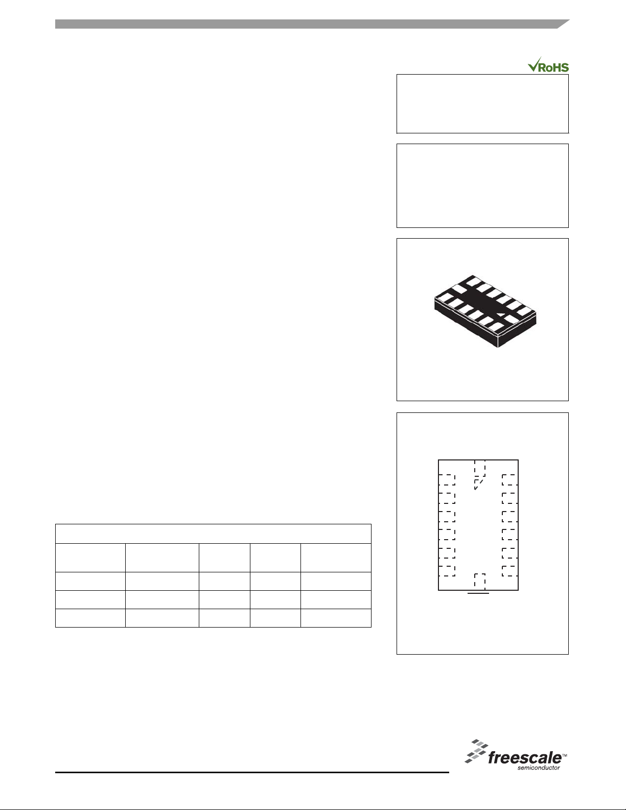
ORDERING INFORMATION
Part Number
MMA7341LT
Temperature
Range
-40 to +85°C 1977-01 LGA-14 Tray
Package
Drawing
Package Shipping
MMA7341L
MMA7341L: XYZ AXIS
ACCELEROMETER
±3g, ±11g
Bottom View
14 LEAD
LGA
CASE 1977-01
Top View
N/C
N/C
X
Y
Z
V
V
123456
OUT
OUT
OUT
SS
DD
14
7
Self Test
N/C
N/C
g-Select
N/C
8 9 10 11 12 13
N/C
MMA7341LR1
MMA7341LR2
© Freescale Semiconductor, Inc., 2008. All rights reserved.
-40 to +85°C 1977-01 LGA-14 7” Tape & Reel
-40 to +85°C 1977-01 LGA-14 13” Tape & Reel
Sleep
Figure 1. Pin Connections
Page 2
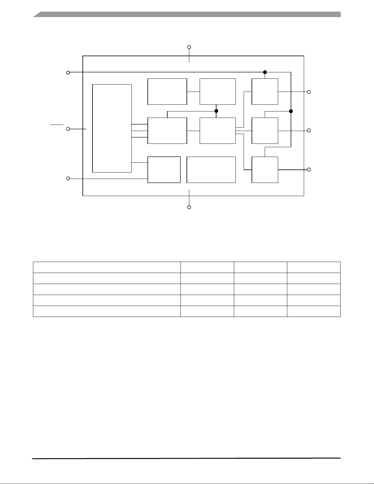
g-Select
g-Select
V
V
DD
DD
Sleep
Sleep
Self Test
Self Test
G-CELL
G-CELL
SENSOR
SENSOR
OSCILLATOR
OSCILLATOR
C to V
C to V
CONVERTER
CONVERTER
SELFTEST
SELFTEST
CLOCK
CLOCK
GEN
GEN
GAIN
GAIN
+
+
FILTER
FILTER
CONTROL LOGIC
CONTROL LOGIC
NVM TRIM
NVM TRIM
CIRCUITS
CIRCUITS
V
V
SS
SS
X-TEMP
X-TEMP
COMP
COMP
Y-TEMP
Y-TEMP
COMP
COMP
Z-TEMP
Z-TEMP
COMP
COMP
Figure 2. Simplified Accelerometer Functional Block Diagram
Table 1. Maximum Ratings
(Maximum ratings are the limits to which the device can be exposed without causing permanent damage.)
X
X
OUT
OUT
Y
Y
OUT
OUT
Z
Z
OUT
OUT
Rating Symbol Value Unit
Maximum Acceleration (all axis) g
Supply Voltage V
Drop Test
Storage Temperature Range T
1. Dropped onto concrete surface from any axis.
(1)
ELECTRO STATIC DISCHARGE (ESD)
WARNING: This device is sensitive to electrostatic
discharge.
Although the Freescale accelerometer contains internal
2000 V ESD protection circuitry, extra precaution must be
taken by the user to protect the chip from ESD. A charge of
over 2000 volts can accumulate on the human body or
associated test equipment. A charge of this magnitude can
alter the performance or cause failure of the chip. When
handling the accelerometer, proper ESD precautions should
be followed to avoid exposing the device to discharges which
may be detrimental to its performance.
max
DD
D
drop
stg
±5000 g
-0.3 to +3.6 V
1.8 m
-40 to +125 °C
MMA7341L
Sensors
2 Freescale Semiconductor
Page 3
Table 2. Operating Characteristics
Unless otherwise noted: -40°C < TA < 85°C, 2.2 V < VDD < 3.6 V, Acceleration = 0g, Loaded output
(1)
Characteristic Symbol Min Typ Max Unit
Operating Range
Supply Voltage
Supply Current
Supply Current at Sleep Mode
Operating Temperature Range
(2)
(3)
(4)
(4)
V
DD
I
DD
I
DD
T
A
2.2
—
—
-40
3.3
400
3
—
3.6
600
10
+85
V
μA
μA
°C
Acceleration Range, X-Axis, Y-Axis, Z-Axis
g-Select: 0
g-Select: 1
g
FS
g
FS
—
—
±3
±11
—
—
g
g
Output Signal
Zero g (T
(4)
Zero g
= 25°C, VDD = 3.3 V)
A
(5), (6)
V
OFF
V
, T
OFF
A
1.551
-2.0
1.65
±0.5
1.749
+2.0
V
mg/°C
Sensitivity (TA = 25°C, VDD = 3.3 V)
3g
11g
Sensitivity
S
3g
S
(4)
S,T
11g
A
413.6
106
-0.0075
440
117.8
±0.002
466.4
129.6
+0.0075
mV/g
mV/g
%/°C
Bandwidth Response
XY
Z
Output Impedance
f
-3dBXY
f
-3dBZ
Z
O
—
—
—
400
300
32
—
—
—
Hz
Hz
kΩ
Self Test
Output Response
X
, Y
OUT
Z
OUT
Input Low
Input High
OUT
Δg
Δg
STXY
STZ
V
IL
V
IH
+0.05
+0.8
V
0.7 V
SS
DD
-0.1
+1.0
—
—
—
+1.2
0.3 V
V
DD
DD
g
g
V
V
Noise
Power Spectral Density RMS (0.1 Hz – 1 kHz)
(4)
n
PSD
— 350 — μg/
Hz
Control Timing
Power-Up Response Time
Enable Response Time
Self Test Response Time
(7)
(8)
(9)
t
RESPONSE
t
ENABLE
t
ST
—
—
—
1.0
0.5
2.0
2.0
2.0
5.0
ms
ms
ms
Sensing Element Resonant Frequency
XY
Z
Internal Sampling Frequency
f
GCELLXY
f
GCELLZ
f
CLK
—
—
—
6.0
3.4
11
—
—
—
kHz
kHz
kHz
Output Stage Performance
Full-Scale Output Range (I
Nonlinearity, X
Cross-Axis Sensitivity
OUT
, Y
OUT
(10)
= 3 µA) V
OUT
, Z
OUT
FSO
NL
OUT
V
XY, XZ, YZ
VSS+0.1 — VDD–0.1 V
-1.0 — +1.0 %FSO
-5.0 — +5.0 %
1. For a loaded output, the measurements are observed after an RC filter consisting of an internal 32kΩ resistor and an external 3.3nF capacitor
(recommended as a minimum to filter clock noise) on the analog output for each axis and a 0.1μF capacitor on V
bandwidth is determined by the Capacitor added on the output. f = 1/2π * (32 x 10
3
) * C. C = 3.3 nF corresponds to BW = 1507HZ, which is
- GND. The output sensor
DD
the minimum to filter out internal clock noise.
2. These limits define the range of operation for which the part will meet specification.
3. Within the supply range of 2.2 and 3.6 V, the device operates as a fully calibrated linear accelerometer. Beyond these supply limits the device
may operate as a linear device but is not guaranteed to be in calibration.
4. This value is measured with g-Select in 3g mode.
5. The device can measure both + and – acceleration. With no input acceleration the output is at midsupply. For positive acceleration the output
will increase above V
/2. For negative acceleration, the output will decrease below VDD/2.
DD
6. For optimal 0g offset performance, adhere to AN3484 and AN3447.
7. The response time between 10% of full scale V
input voltage and 90% of the final operating output voltage.
DD
8. The response time between 10% of full scale Sleep Mode input voltage and 90% of the final operating output voltage.
9. The response time between 10% of the full scale self test input voltage and 90% of the self test output voltage.
10. A measure of the device’s ability to reject an acceleration applied 90° from the true axis of sensitivity.
MMA7341L
Sensors
Freescale Semiconductor 3
Page 4
PRINCIPLE OF OPERATION
The Freescale accelerometer is a s urface-micromachined
integrated-circuit accelerometer.
The device consists of a surface micromachined
capacitive sensing cell (g-cell) and a signal conditioning ASIC
contained in a single package. The sensing element is sealed
hermetically at the wafer level using a bulk micromachined
cap wafer.
The g-cell is a mechanical structure formed from
semiconductor materials (polysilicon) using semiconductor
processes (masking and etching). It can be modeled as a set
of beams attached to a movable central mass that move
between fixed beams. The movable beams can be deflected
from their rest position by subjecting the system to an
acceleration (Figure 3).
As the beams attached to the central mass move, the
distance from them to the fixed beams on one side will
increase by the same amount that the distance to the fixed
beams on the other side decreases. The change in distance
is a measure of acceleration.
The g-cell beams form two back-to-back capacitors
(Figure 3). As the center beam moves with acceleration, the
distance between the beams changes and each capacitor's
value will change, (C = Aε/D). Where A is the area of the
beam, ε is the dielectric constant, and D is the distance
between the beams.
The ASIC uses switched capacitor techniques to measure
the g-cell capacitors and extract the acceleration data from
the difference between the two capacitors. The ASIC also
signal conditions and filters (switched capacitor) the signal,
providing a high level output voltage that is ratiometric and
proportional to acceleration.
Acceleration
g-Select
The g-Select feature allows for the selection between two
sensitivities. Depending on the logic input placed on pin 10,
the device internal gain will be changed allowing it to function
with a 3g or 11g sensitivity (Table 3). This feature is ideal
when a product has applications requiring two different
sensitivities for optimum performance. The sensitivity can be
changed at anytime during the operation of the product. The
g-Select pin can be left unconnected for applications
requiring only a 3g sensitivity as the device has an internal
pull-down to keep it at that sensitivity (440mV/g)).
Table 3. g-Select Pin Description
g-Select g-Range Sensitivity
0 3g 440 mV/g
1 11g 117.5 mV/g
Sleep Mode
The 3 axis accelerometer provides a Sleep Mode that is
ideal for battery operated products. When Sleep Mode is
active, the device outputs are turned off, providing significant
reduction of operating current. A low input signal on pin 7
(Sleep Mode) will place the device in this mode and reduce
the current to 3 μA typ. For lower power consumption, it is
recommended to set g-Select to 3g mode. By placing a high
input signal on pin 7, the device will resume to normal mode
of operation.
Filtering
The 3 axis accelerometer contains an onboard single-pole
switched capacitor filter. Because the filter is realized using
switched capacitor techniques, there is no requirement for
external passive components (resistors and capacitors) to set
the cut-off frequency.
Ratiometricity
Ratiometricity simply means the output offset voltage and
sensitivity will scale linearly with applied supply voltage. That
is, as supply voltage is increased, the sensitivity and offset
increase linearly; as supply voltage decreases, offset and
sensitivity decrease linearly. This is a key feature when
interfacing to a microcontroller or an A/D converter because
Figure 3. Simplified Transducer Physical Model
SPECIAL FEA T URES
it provides system level cancellation of supply induced errors
in the analog to digital conversion process.
Self Test
The sensor provides a self test feature that allows the
verification of the mechanical and electrical integrity of the
accelerometer at any time before or after installation.
This
feature is critical in applications such as hard disk drive
protection where system integrity must be ensured over the
life of the product. Customers can use self test to verify the
solderability to confirm that the part was mounted to the PCB
correctly. When the self test function is initiated, an
electrostatic force is applied to each axis to cause it to deflect.
The x- and y-axis are deflected slightly while the z-axis is
trimmed to deflect 1g. This procedure assures that both the
mechanical (g-cell) and electronic sections of the
accelerometer are functioning.
MMA7341L
Sensors
4 Freescale Semiconductor
Page 5

Pin Descriptions
Top View
N/C
14
123456
7
Sleep
Self Test
N/C
N/C
g-Select
N/C
8 9 10 11 12 13
N/C
X
Y
Z
N/C
OUT
OUT
OUT
V
V
SS
DD
Figure 4. Pinout Description
Table 4. Pin Descriptions
Pin No.
Pin Name Description
1 N/C No internal connection
2X
3Y
4Z
5 V
6V
OUT
OUT
OUT
SS
DD
7Sleep
Leave unconnected
X direction output voltage
Y direction output voltage
Z direction output voltage
Power Supply Ground
Power Supply Input
Logic input pin to enable product or Sleep Mode
8 N/C No internal connection
Leave unconnected
9 N/C No internal connection
Leave unconnected
10 g-Select Logic input pin to select g level
11 N/C Unused for factory trim
12 N/C Unused for factory trim
Leave unconnected
Leave unconnected
13 Self Test Input pin to initiate Self Test
14 N/C Unused for factory trim
V
DD
0.1 μF
Leave unconnected
Logic
Input
Logic
Input
10
13
6
5
g-Select
Self Test
MMA7341L
V
DD
V
SS
0g-Detect
X
OUT
Y
OUT
9
2
3
3.3 nF
3.3 nF
BASIC CONNECTIONS
PCB Layout
g-Select
Self Test
Accelerometer
Figure 6. Recommended PCB Layout for Interfacing
NOTES:
1. Use 0.1 µF capacitor on V
source.
2. Physical coupling distance of the accelerometer to
the microcontroller should be minimal.
3. Place a ground plane beneath the accelerometer to
reduce noise, the ground plane should be attached to
all of the open ended terminals shown in Figure 6.
4. Use a 3.3nF capacitor on the outputs of the
accelerometer to minimi ze clock noise (from the
switched capacitor filter circuit).
5. PCB layout of power and ground should not couple
power supply noise.
6. Accelerometer and microcontroller should not be a
high current path.
7. A/D sampling rate and any external power supply
switching frequency should be selected such that
they do not interfere with the internal accelerometer
sampling frequency (11 kHz for the sampling
frequency). This will prevent aliasing errors.
8. 10MΩ
Z
relationship between the internal 32 kΩ resistor and
the measurement input impedance.
Connection Diagram
POWER SUPPLY
V
V
Sleep
DD
C
SS
V
RH
C
C
P0
P1
P2
X
OUT
Y
OUT
C
C
Z
OUT
C
A/D
A/D
A/D
IN
IN
IN
Accelerometer to Microcontroller
to decouple the power
DD
or higher is recommended on X
to prevent loss due to the voltage divider
OUT
OUT
V
DD
C
C
V
SS
Microcontroller
, Y
and
OUT
Logic
Input
7
Sleep
Z
OUT
4
3.3 nF
Figure 5. Accelerometer with Recommended
MMA7341L
Sensors
Freescale Semiconductor 5
Page 6

Top View
DYNAMIC ACCELERATION
+Y
7
8 9 10 11 12 13
-Y
14-Pin LGA Package
123456
14
STATIC ACCELERATION
Top View
123456
Side View
+X +Z-X
Top
Bottom
: Arrow indicates direction of package movement.
Direction of Earth's gravity field.*
-Z
123456
@ +1g = 2.09 V
X
OUT
@ 0g = 1.65 V
Y
OUT
@ 0g = 1.65 V
Z
OUT
7
8 9 10 11 12 13
14
8 9 10 11 12 13
7
X
@ 0g = 1.65 V
OUT
@ +1g = 2.09 V
Y
OUT
@ 0g = 1.65 V
Z
OUT
13 12 11 10 9 8
14 7
1234 56
X
@ 0g = 1.65 V
OUT
@ -1g = 1.21 V
Y
OUT
@ 0g = 1.65 V
Z
OUT
14
7
8 9 10 11 12 13
123456
14
@ -1g = 1.21 V
X
OUT
@ 0g = 1.65 V
Y
OUT
@0g=1.65V
Z
OUT
* When positioned as shown, the Earth’s gravity will result in a positive 1g output.
Side View
Bottom
X
@ 0g = 1.65 V
OUT
@ 0g = 1.65 V
Y
OUT
@ +1g = 2.09 V
Z
OUT
Bottom
X
OUT
Y
OUT
Z
OUT
Top
Top
@ 0g = 1.65 V
@ 0g = 1.65 V
@ -1g =1.21 V
MMA7341L
Sensors
6 Freescale Semiconductor
Page 7

X-T C O mg/ d egC
X-TCS %/degC
LSL USLTarget
-2 -1 0 1 2
Y-T C O mg/ d egC
LSL USLTarget
-2 -1 0 1 2
Z-TCO mg/degC
LSL USLTarget
-0.01 -0.005 0 .005 .01
Y-TCS %/degC
LSL USLTarget
-0.01 -0.005 0 .005 .01
Z-TCS %/degC
LSL USLTarget
-2 -1 0 1 2
LSL USLTarget
-0.01 -0.005 0 .005 .01
Figure 7. MMA7341L Temperature Coefficient of Offset (TCO) and
Temperature Coefficient of Sensitivity (TCS) Distribution Charts
MMA7341L
Sensors
Freescale Semiconductor 7
Page 8

MINIMUM RECOMMENDED FOOTPRINT FOR SURFACE MOUNTED APPLICATIONS
PCB Mounting Recommendations
MEMS based sensors are sensitive to Printed Circuit
Board (PCB) reflow processes. For optimal zero-g offset after
PCB mounting, care must be taken to PCB layout and reflow
conditions. Reference application note AN3484 for best
practices to minimize the zero-g offset shift after PCB
mounting.
Surface mount board layout is a critical portion of the total
design. The footprint for the surface mount packages must be
the correct size to ensure proper solder connection interface
between the board and the package.
With the correct footprint, the packages will self-align when
subjected to a solder reflow process. It is always
recommended to design boards with a solder mask layer to
avoid bridging and shorting between solder pads.
10x0.8
1
6
13
6x2
8
14x0.6
14x0.9
Figure 8. LGA 14-Lead, 5 x 3 mm Die Sensor
12x1
MMA7341L
Sensors
8 Freescale Semiconductor
Page 9

PACKAGE DIMENSIONS
CASE 1977-01
ISSUE A
14-LEAD LGA
MMA7341L
Sensors
Freescale Semiconductor 9
Page 10

PACKAGE DIMENSIONS
CASE 1977-01
ISSUE A
14-LEAD LGA
MMA7341L
Sensors
10 Freescale Semiconductor
Page 11

How to Reach Us:
Home Page:
www.freescale.com
Web Support:
http://www.freescale.com/support
USA/Europe or Locations Not Listed:
Freescale Semiconductor, Inc.
Technical Information Center, EL516
2100 East Elliot Road
Tempe, Arizona 85284
+1-800-521-6274 or +1-480-768-2130
www.freescale.com/support
Europe, Middle East, and Africa:
Freescale Halbleiter Deutschland GmbH
Technical Information Center
Schatzbogen 7
81829 Muenchen, Germany
+44 1296 380 456 (English)
+46 8 52200080 (English)
+49 89 92103 559 (German)
+33 1 69 35 48 48 (French)
www.freescale.com/support
Japan:
Freescale Semiconductor Japan Ltd.
Headquarters
ARCO Tower 15F
1-8-1, Shimo-Meguro, Meguro-ku,
Tokyo 153-0064
Japan
0120 191014 or +81 3 5437 9125
support.japan@freescale.com
Asia/Pacific:
Freescale Semiconductor Hong Kong Ltd.
Technical Information Center
2 Dai King Street
Tai Po Industrial Estate
Tai Po, N.T., Hong Kong
+800 2666 8080
support.asia@freescale.com
For Literature Requests Only:
Freescale Semiconductor Literature Distribution Center
P.O. Box 5405
Denver, Colorado 80217
1-800-441-2447 or 303-675-2140
Fax: 303-675-2150
LDCForFreescaleSemiconductor@hibbertgroup.com
Information in this document is provided solely to enable system and software
implementers to use Freescale Semiconductor products. There are no express or
implied copyright licenses granted hereunder to design or fabricate any integrated
circuits or integrated circuits base d on the information in this document.
Freescale Semiconductor reserves the right to make changes without further notice to
any products herein. Freescale Semiconductor makes no warranty, representation or
guarantee regarding the suitability of its products for any particular purpose, nor does
Freescale Semiconductor assume any liability arising out of the application or use of any
product or circuit, and specifically disclaims any and all liability, including without
limitation consequential or incidental damages. “Typical” parameters that may be
provided in Freescale Semiconductor data sheet s and/or specifications can and do vary
in different applications and actual performance may vary over time. All operating
parameters, including “Typicals”, must be validated for each customer application by
customer’s technical experts. Freescale Semiconductor does not convey any licen se
under its patent rights nor the rights of others. Freescale Semiconductor products are
not designed, intended, or authorized for use as components in systems intended for
surgical implant into the body, or other applications intended to support or sustain life,
or for any other application in which the failure of the Freescale Semiconduct or product
could create a situation where personal injury or death may occur. Should Buyer
purchase or use Freescale Semiconductor products for any such unintended or
unauthorized application, Buyer shall indemnify and hold Freescale Semiconductor and
its officers, employees, subsidiaries, affiliates, and distributors harmless against all
claims, costs, damages, and expenses, and reasonable attorney fees arising out of,
directly or indirectly, any claim of personal injury or death associated with such
unintended or unauthorized use, even if such claim alleges that Freescale
Semiconductor was negligent regarding the design or manufacture of the part.
Freescale™ and the Freescale logo are trademarks of Freescale Semiconductor, Inc.
All other product or service names are the property of their respective owners.
© Freescale Semiconductor, Inc. 2008. All rights reserved.
MMA7341L
Rev. 0
04/2008
RoHS-compliant and/or Pb-free versions of Freescale products have the functionality and electrical
characteristics of their non-RoHS-compliant and/or non-Pb-free counterparts. For further
information, see http:/www.freescale.com or contact your Freescale sales representative.
For information on Freescale’s Environment al Product s program, go to http://www.freescale.com/epp.
 Loading...