

Page 1
Freescale Semiconductor
Advance Information
查询"MM908E425"供应商
Integrated Quad Half H-Bridge
Document Number: MM908E425
Rev. 1.0, 8/2006
with Power Supply, Embedded
MCU, and LIN Serial
Communication
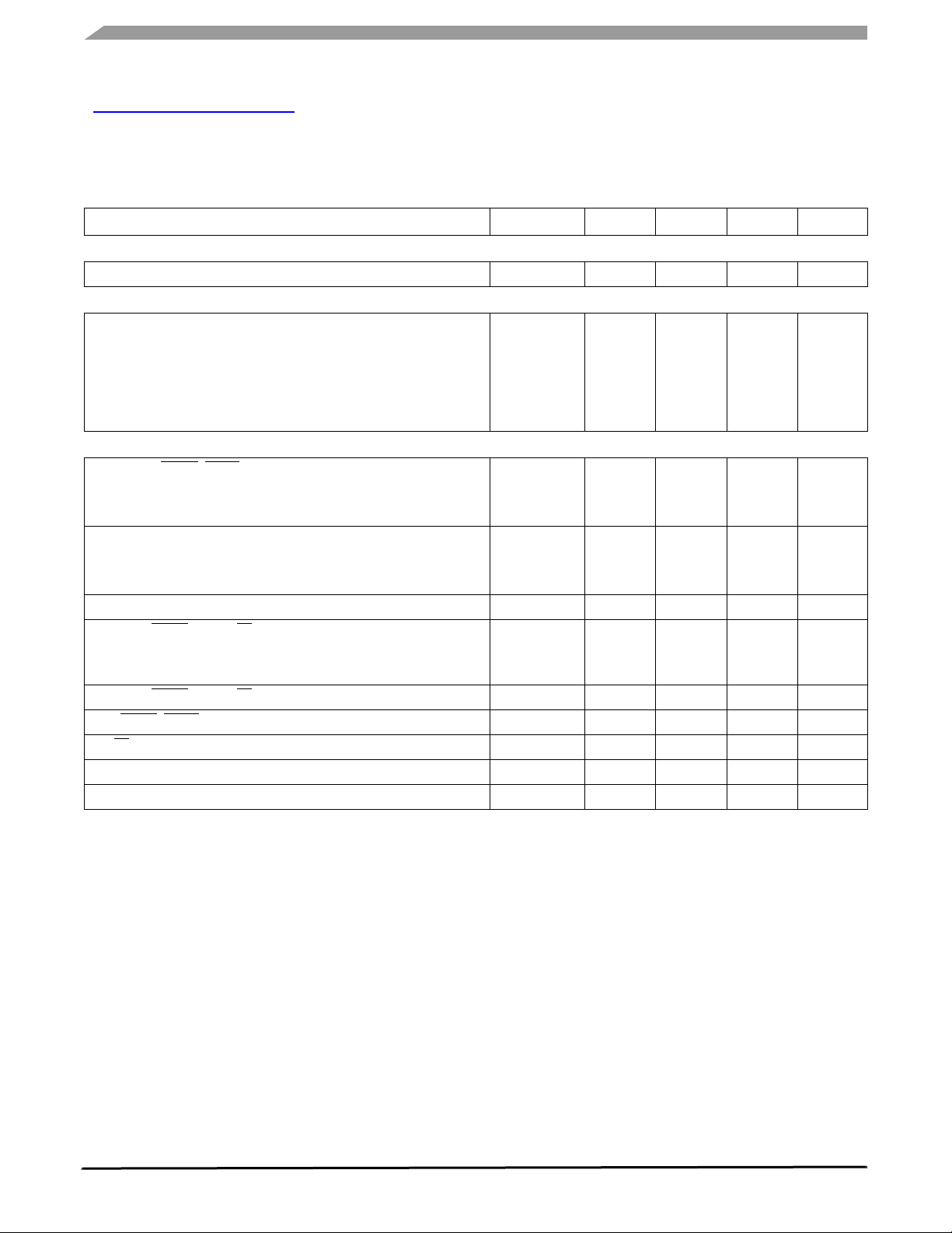
The 908E425 is an integrated single-package solution including a
high-performance HC08 microcontroller with a SMARTMOS
analog control IC. The HC08 includes Flash Memory, a timer,
Enhanced Serial Communications Interface (ESCI), an Analog-toDigital Converter (ADC), Serial Peripheral Interface (SPI) (only
internal), and an Internal Clock Generator (ICG) module. The analog
control die provides fully protected H-Bridge/high-side outputs,
voltage regulator, autonomous watchdog with cyclic wake-up, and
Local Interconnect Network (LIN) physical layer.
The single-package solution, together with LIN, provides optimal
application performance adjustments and space-saving PCB design.
It is well suited for the control of automotive mirror, door lock, and
light-levelling applications.
Features
• High-Performance M68HC908EY16 Core
• 16 K Bytes of On-Chip Flash Memory
• 512 Bytes of RAM
• Internal Clock Generation Module
• Two 16-bit, 2-Channel Timers
• 10-Bit Analog-to-Digital Converter
• LIN Physical Layer
• Autonomous Watchdog with Cyclic Wakeup
• Three Two-Pin Hall-Effect Sensor Input Ports
• One Analog Input with Switchable C urr en t So urce
• Four Low RDS (ON) Half-Bridge Outputs
• One Low RDS (ON) High-Side Output
• 13 Micro Controller I/Os
3
VSUP
ARCHIVE INFORMATION
LIN
VREFH
VDDA
EVDD
VDD
VREFL
VSSA
EVSS
VSS
RST
RST_A
IRQ
IRQ_A
SS
PTB1/AD1
RXD
PTE1/RXD
PTD1/TACH1
FGEN
BEMF
PTD0/TACH0/BEMF
TM
908E425
GND
2
EP
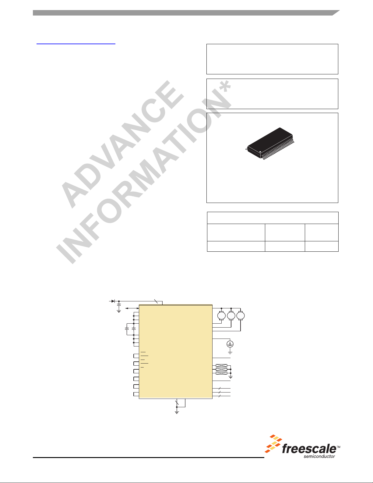
MM908E425AIDWB
HB1
HB2
HB3
HB4
HS
HVDD
H1
H2
H3
PA1
PORT A I/OS
PORT B I/OS
PORT C I/OS
908E425
H-BRIDGE POWER SUPPLY WITH
EMBEDDED MCU AND LIN
DWB SUFFIX
98ASA10712D
54-PIN SOICWB-EP
ORDERING INFORMATION
Device
M M M
High-Side
Switchable Internal
2-Terminal Hall-Effect
Analog Input with
Current Source
Microcontroller
4 Half-Bridges
Controlling
3 Loads
Output
V
Output
DD
Three
Sensor Inputs
Ports
Temperature
Range (T
0°C to 85°C 54 SOICW EP
)
A
ARCHIVE INFORMATION
Package
Figure 1. 908E425 Simplified Application Diagram
* This document contains certain information on a new product.
Specifications and information herein are subject to change without notice.
© Freescale Semiconductor, Inc., 2006. All rights reserved.
Page 2
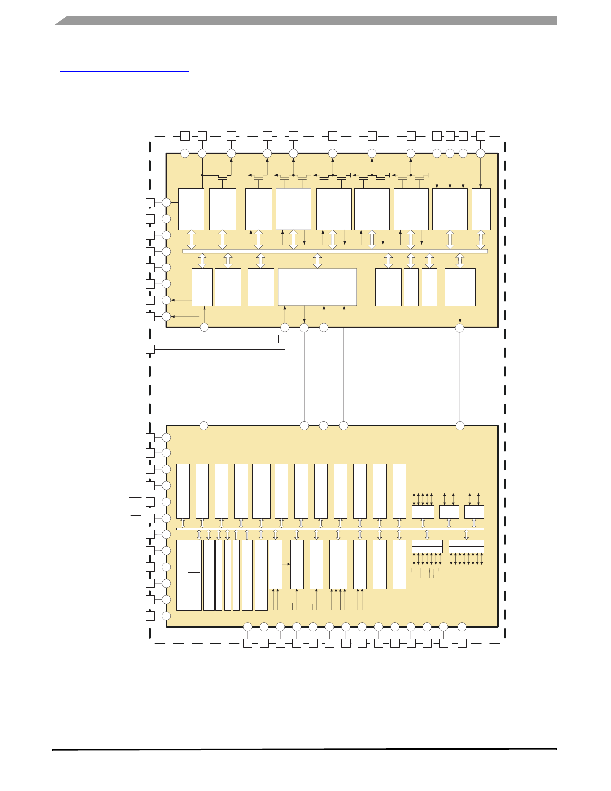
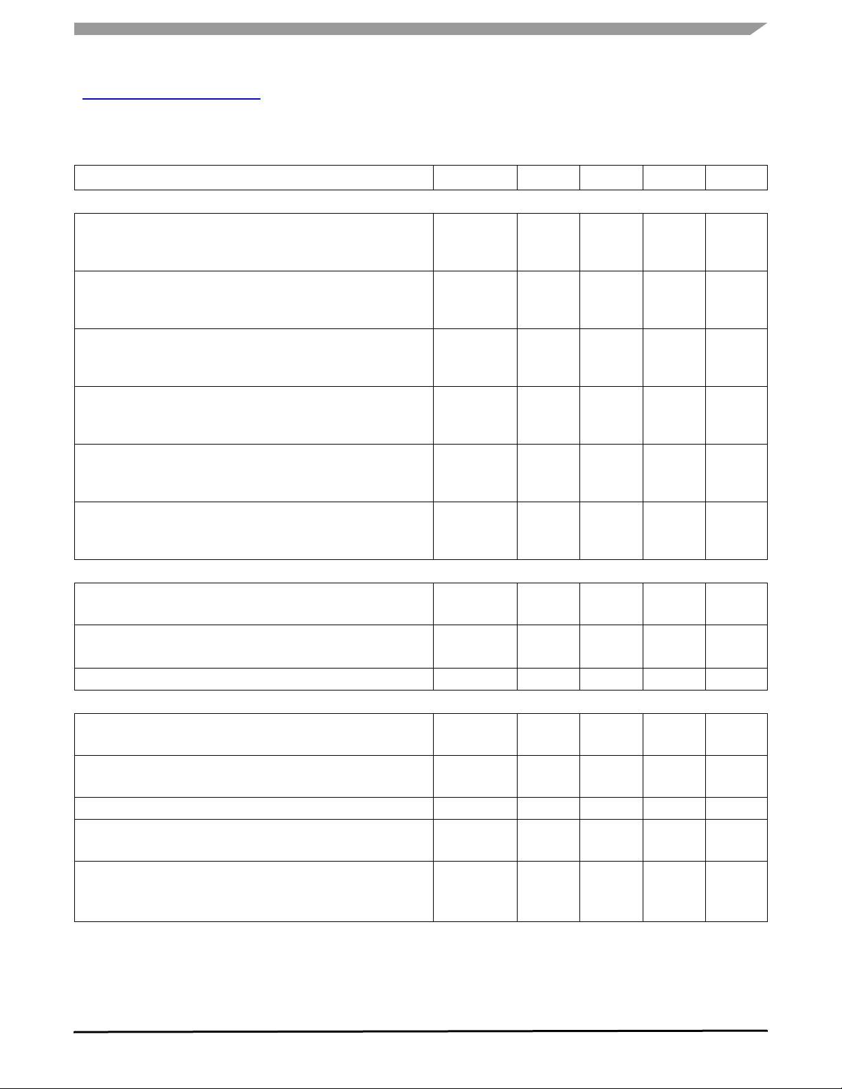
BLOCK DIAGRAM
查询"MM908E425"供应商
GND1-2
VSUP1-3
RST_A
IRQ_A
BEMF
FGEN
LIN
RXD
VSS
Voltage
VDD
Regulator
Layer
LIN Physical
HVDD
Driver &
Diagnostic
Switched VDD
Module
Reset Control
BLOCK DIAGRAM
HS
VSUP
High Side
FGEN
Interrupt
Driver &
Diagnostic
Control
Module
VSUP
Half Bridge
FGEN
HB1
Driver &
Diagnostic
BEMF
SPI
VSUP
FGEN
&
HB2
Driver &
Half Bridge
CONTROL
Diagnostic
BEMF
VSUP
FGEN
HB3
Driver &
Diagnostic
Half Bridge
BEMF
VSUP
FGEN
Watchdog
Autonomous
HB4
Driver &
Diagnostic
Half Bridge
BEMF
Chip Temp
H1H2H3
VSUP
Prescaler
Hall-Effect
Sensor Inputs
Analog
Analog Input
Multiplexer
PA1
Source
with Current
ARCHIVE INFORMATION
PTD1/TACH1
PTD0/TACH0
ARCHIVE INFORMATION
SS
PTE1/RXD
PTB1/AD1
RST
IRQ
VREFL
VSSA
EVSS
EVDD
VDDA
VREFH
TXD
PTE0/TXD
Break Module
5-Bit Keyboard
Interrupt Module
Single Breakpoint
Internal Bus
ALU
M68HC08 CPU
CPU
Registers
Control and Status Register,
2-channel Timer
2-Channel Timer
Interface Module A
Interface Module B
64 Bytes
User RAM, 512 Bytes
Monitor ROM, 310 Bytes
User Flash, 15,872 Bytes
Flash Programming (burn in)
Communication
Enhanced Serial
Interface Module
Computer Operating
Internal Clock
Generator Module
36 Bytes
ROM, 1024 Bytes
User Flash Vector Space,
OSC2
OSC1
SS
MISO
PTC0/MISO
Properly Module
Interface Module
Serial Pheripheral
Integration Module
24 Internal System
RST
MOSI
SPSCK
PTC1/MOSI
PTA5/SPSCK
Module
Timebase Module
Periodic Wake-Up
Configuration Register
Module
Module
Digital Converter
10 Bit Analog-to-
Single External IRQ
IRQ
VDDA
VREFL
VSSA
VREFH
Arbiter Module
POWER
VDD
VSS
BEMF Module
Prescaler Module
Module
Security Module
Power-On Reset
PTC4/OSC1
PTC3/OSC2
PTC2/MCLK
PTC1/MOSI
PORT CPORT D
DDRCDDRD
PTA6/SS
PTA3/KBD3
PTA4/KBD4
PTA5/SPSCK
PTC0/MISO
DDRA
PORT A
PTA2/KBD2
PTA1/KBD1
PTA0/KBD0
ADOUT
PTB0/AD0
PTD1/TACH1
PTD0/TACH0
PTB5/AD5
PTB6/AD6/TBCH0
PTB7/AD7/TBCH1
PTE1/RxD
DDRB
PORT B
PTB4/AD4
PTB3/AD3
PTB2/AD2
MCU Die Analog Die
PTE0/TxD
PORT E
DDRE
PTB1/AD1
PTB0/AD0
PTA0/KBD0
PTA1/KBD1
PTA2/KBD2
PTA3/KBD3
PTB3/AD3
PTA4/KBD4
PTB5/AD5
PTB4/AD4
PTC2/MCLK
PTB6/AD6/TBCH0
PTB7/AD7/TBCH1
PTC3/OSC2
FLSVPP
PTC4/OSC1
Figure 2. 908E425 Simplified Internal Block Diagram
908E425
Analog Integrated Circuit Device Data
2 Freescale Semiconductor
Page 3
查询"MM908E425"供应商
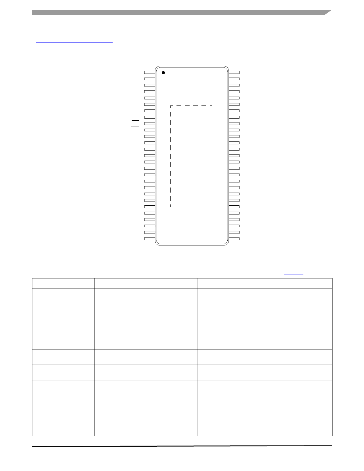
PIN CONNECTIONS
PIN CONNECTIONS
PTB7/AD7/TBCH1
PTB6/AD6/TBCH0
PTC4/OSC1
PTC3/OSC2
PTC2/MCLK
PTB5/AD5
PTB4/AD4
PTB3/AD3
IRQ
RST
PTB1/AD1
PTD0/TACH0/BEMF
PTD1/TACH1
NC
FGEN
BEMF
RST_A
IRQ_A
SS
LIN
NC
NC
HB1
VSUP1
GND1
HB2
VSUP2
1
2
3
4
5
6
7
8
9
10
11
12
13
14
15
16
17
18
19
20
21
22
23
24
25
26
27
Exposed
Pad
54
53
52
51
50
49
48
47
46
45
44
43
42
41
40
39
38
37
36
35
34
33
32
31
30
29
28
PTA0/KBD0
PTA1/KBD1
PTA2/KBD2
FLSVPP
PTA3/KBD3
PTA4/KBD4
VREFH
VDDA
EVDD
EVSS
VSSA
VREFL
PTE1/RXD
RXD
VSS
PA1
VDD
H1
H2
H3
HVDD
NC
HB4
VSUP3
GND2
HB3
HS
ARCHIVE INFORMATION
Table 1. 908E425 Pin Definitions
A functional description of each pin can be found in the Functional Pin Description section beginning on page 14.
Figure 3. 908E425 Pin Connections (Transparent Package Top View)
Pin Function Pin Pin Name Formal Name Definition
MCU 1
MCU 3
MCU 9 IRQ External Interrupt
ARCHIVE INFORMATION
MCU 10 RST External Reset
MCU 12
– 14, 21, 22, 33 NC No Connect
MCU 42 PTE1/ RXD Port E I /O
MCU 43
2
6
7
8
11
4
5
13
48
PTB7/AD7/TBCH1
PTB6/AD6/TBCH0
PTB5/AD5
PTB4/AD4
PTB3/AD3
PTB1/AD1
PTC4/OSC1
PTC3/OSC2
PTC2/MCLK
PTD0/TACH0/BEMF
PTD1/TACH1
VREFL
VREFH
ADC References
Port B I/Os
Port C I/Os
Input
Port D I /Os
These pins are special-function, bidirectional I/O port pins that
are shared with other functional modules in the MCU.
These pins are special-function, bidirectional I/O port pins that
are shared with other functional modules in the MCU.
This pin is an asynchronous external interrupt input pin.
This pin is bidirectional, allowing a reset of the entire system. It
is driven low when any internal reset source is asserted.
These pins are special-function, bidirectional I /O port pins that
are shared with other functional modules in the MCU.
Not connected.
This pin is a special-function, bidirectional I/O port pin that can
is shared with other functional modules in the MCU.
These pins are the reference voltage pins for the analog-to-
digital converter (ADC).
908E425
Analog Integrated Circuit Device Data
Freescale Semiconductor 3
Page 4

PIN CONNECTIONS
查询"MM908E425"供应商
Table 1. 908E425 Pin Definitions (continued)
A functional description of each pin can be found in the Functional Pin Description section beginning on page 14.
Pin Function Pin Pin Name Formal Name Definition
MCU 44
47
MCU 45
46
MCU 49
MCU 51 FLSVPP Test Pin
Analog 15 FGEN Current Limitation
Analog 16 BEMF Back Electromagnetic
Analog 17 RST_A Internal Reset
Analog 18 IRQ_A Internal Interrupt
Analog 19 SS Slave Select
Analog 20 LIN LIN Bus
Analog 23
Analog 24
Analog 25
Analog 28 HS High-Side Output
Analog 34 HVDD Switchable
Analog 35
Analog 38 VDD Voltage Regulator
ARCHIVE INFORMATION
Analog 39 PA1 Analog Input
Analog 40 VSS Voltage Regulator
Analog 41 RXD LIN Transceiver
– EP Exposed Pad Exposed Pad
50
52
53
54
26
29
32
27
31
30
36
37
VSSA
VDDA
EVSS
EVDD
PTA4/KBD4
PTA3/KBD3
PTA2/KBD2
PTA1/KBD1
PTA0/KBD0
HB1
HB2
HB3
HB4
VSUP1
VSUP2
VSUP3
GND1
GND2
H3
H2
H1
ADC Supply
MCU Power Supply
Port A I /Os
Frequency Input
Force Output
Output
Half-Bridge Outputs
Power Supply Pins
Power Ground Pins
V
DD
Hall-Effect Sensor
Output
Ground
Output
Pins
Pins
Output
Inputs
These pins are the power supply pins for the analog-to-digital
converter.
These pins are the ground and power supply pins, respectively.
The MCU operates from a single power supply.
These pins are special-function, bidirectional I/O port pins that
are shared with other functional modules in the MCU.
For test purposes only. Do not connect in the application.
This is the input pin for the half-bridge current limitation and the
high-side inrush current limiter PWM frequency.
This pin gives the user information about back electromagnetic
force (BEMF).
This pin is the bidirectional reset pin of the analog die.
This pin is the interrupt output pin of the analog die indicating
errors or wake-up events.
This pin is the SPI slave select pin for the analog chip.
This pin represents the single-wire bus transmitter and receiver.
This device includes power MOSFETs configured as four half-
bridge driver outputs. These outputs may be configured for step
motor drivers, DC motor drivers, or as high-side and low-side
switches.
These pins are device power supply pins.
These pins are device power ground connections.
This output pin is a low R
This pin is a switchable VDD output for driving resistive loads
requiring a regulated 5.0
sensors.
These pins provide inputs for Hall-effect sensors and switches.
The + 5.0 V voltage regulator output pin is intended to supply
the embedded microcontroller.
This pin is an analog input port with selectable source values.
Ground pin for the connection of all non-power ground
connections (microcontroller and sensors).
This pin is the output of LIN transceiver.
The exposed pad pin on the bottom side of the package
conducts heat from the chip to the PCB board.
high-side switch.
DS(ON)
V supply; e.g., 3-pin Hall-effect
ARCHIVE INFORMATION
908E425
Analog Integrated Circuit Device Data
4 Freescale Semiconductor
Page 5
ELECTRICAL CHARACTERISTICS
MAXIMUM RATINGS
查询"MM908E425"供应商
ELECTRICAL CHARACTERISTICS
MAXIMUM RATINGS
Table 2. Maximum Ratings
All voltages are with respect to ground unless otherwise noted. Exceeding these ratings may cause a malfunction or
permanent damage to the device.
Ratings Symbol Value Unit
ELECTRICAL RATINGS
Supply Voltage
Analog Chip Supply Voltage under Normal Operation, Steady State
(1)
(5)
= 200 pF, R
ZAP
ZAP
Analog Chip Supply Voltage under Transient Conditions
Microcontroller Chip Supply Voltage
Input Pin Voltage
Analog Chip
Microcontroller Chip
Maximum Microcontroller Current per Pin
All Pins Except VDD, VSS, PTA0 : PTA6, PTC0 : PTC1
Pins PTA0 : PTA6, PTC0 : PTC1
Maximum Microcontroller VSS Output Current
Maximum Microcontroller VDD Input Current
LIN Supply Voltage
Normal Operation (Steady-State)
Transient Conditions
ESD Voltage
Human Body Model (HBM)
Machine Model (MM)
Charge Device Model (CDM)
THERMAL RATINGS
Storage Temperature
Ambient Operating Temperature
Operating Case Temperature
Operating Junction Temperature
Peak Package Reflow Temperature During Solder Mounting
Notes
1. Transient capability for pulses with a time of t < 0.5 sec.
ARCHIVE INFORMATION
2. ESD voltage testing is performed in accordance with the Human Body Model (C
3. The limiting factor is junction temperature, taking into account the power dissipation, thermal resistance, and heat sinking.
4. The temperature of analog and MCU die is strongly linked via the package, but can differ in dynamic load conditions, usually because
5. Pin soldering temperature is for 10 seconds maximum duration. Not designed for immersion soldering. Exceeding these limits may cause
(2)
performed in accordance with the Machine Model (C
Charge Device Model, robotic (C
of higher power dissipation on the analog die. The analog die temperature must not exceed 150°C under these conditions.
malfunction or permanent damage to the device.
(1)
(3)
(4)
= 4.0 pF).
ZAP
V
SUP(SS)
V
SUP(PK)
V
DD
V
(ANALOG)
IN
V
(MCU)
IN
I
(1)
PIN
I
(2)
PIN
I
MVSS
I
MVDD
V
BUS(SS)
V
BUS(DYNAMIC)
V
ESD
T
STG
T
A
T
C
T
J
T
SOLDER
= 100 pF, R
ZAP
= 0 Ω, ESD voltage testing is performed in accordance with
- 0.3 to 28
- 0.3 to 40
- 0.3 to 6.0
- 0.3 to 5.5
- 0.3 to VDD + 0.3
V
SS
±15
± 25
100 mA
100 mA
-18 to 28
40
± 3000
± 150
± 500
– °C
0 to 85 °C
0 to 85 °C
0 to 125 °C
245 °C
= 1500 Ω), ESD voltage testing is
ZAP
ARCHIVE INFORMATION
V
V
mA
V
V
908E425
Analog Integrated Circuit Device Data
Freescale Semiconductor 5
Page 6
ELECTRICAL CHARACTERISTICS
STATIC ELECTRICAL CHARACTERISTICS
查询"MM908E425"供应商
STATIC ELECTRICAL CHARACTERISTICS
Table 3. Static Electrical Characteristics
All characteristics are for the analog chip only. Refer to the 68HC908EY16 specification for characteristics of the
microcontroller chip. Characteristics noted under conditions 9.0 V ≤ V
≤ 16 V, 0°C ≤ TJ ≤ 125°C unless otherwise noted.
SUP
Typical values noted reflect the approximate parameter mean at TA = 25°C under nominal conditions unless otherwise noted.
Characteristic Symbol Min Typ Max Unit
SUPPLY VOLTAGE
Nominal Operating Voltage
SUPPLY CURRENT
NORMAL Mode
V
= 12 V, Power Die ON (PSON = 1), MCU Operating Using
SUP
Internal Oscillator at 32
ADC Enabled
STOP Mode
V
SUP
DIGITAL INTERFACE RATINGS (ANALOG DIE)
Output Pins RST_A, IRQ_A
Low-State Output Voltage (I
High-State Output Voltage (I
Output Pins BEMF, RXD
Low-State Output Voltage (I
High-State Output Voltage (I
Output Pin RXD – Capacitance
Input Pins RST_A, FGEN, SS
Input Logic Low Voltage
Input Logic High Voltage
Input Pins RST_A, FGEN, SS – Capacitance
Pins RST_A, IRQ_A – Pullup Resistor
Pin SS – Pullup Resistor
Pins FGEN, MOSI, SPSCK – Pulldown Resistor
Pin TXD – Pullup Current Source
Notes
6. STOP mode current will increase if V
7. This parameter is guaranteed by process monitoring but is not production tested.
(6)
= 12 V, Cyclic Wake-Up Disabled
MHz (8.0 MHz Bus Frequency), SPI, ESCI,
= - 1.5 mA)
OUT
= 1.0 μA)
OUT
= - 1.5 mA)
OUT
= 1.5 mA)
OUT
(7)
(7)
exceeds 15 V.
SUP
V
SUP
I
RUN
I
STOP
V
OL
V
OH
V
OL
V
OH
C
IN
V
IL
V
IH
C
IN
R
PULLUP
R
PULLUP
R
PULLDOWN
I
PULLUP
8.0 – 18 V
–
–
–
3.85
–
3.85
– 4.0 – pF
–
3.5
– 4.0 – pF
1
2
– 10 – kΩ
– 60 – kΩ
– 60 – kΩ
– 35 – μA
20
–
–
–
–
–
–
–
–
60
0.4
–
0.4
–
1.5
–
mA
μA
V
V
V
ARCHIVE INFORMATION
ARCHIVE INFORMATION
908E425
Analog Integrated Circuit Device Data
6 Freescale Semiconductor
Page 7
STATIC ELECTRICAL CHARACTERISTICS
ELECTRICAL CHARACTERISTICS
查询"MM908E425"供应商
Table 3. Static Electrical Characteristics (continued)
All characteristics are for the analog chip only. Refer to the 68HC908EY16 specification for characteristics of the
microcontroller chip. Characteristics noted under conditions 9.0 V ≤ V
Typical values noted reflect the approximate parameter mean at TA = 25°C under nominal conditions unless otherwise noted.
Characteristic Symbol Min Typ Max Unit
≤ 16 V, 0°C ≤ TJ ≤ 125°C unless otherwise noted.
SUP
SYSTEM RESETS AND INTERRUPTS
High-Voltage Reset
Threshold
Hysteresis
Low-Voltage Reset
Threshold
Hysteresis
High-Voltage Interrupt
Threshold
Hysteresis
Low-Voltage Interrupt
Threshold
Hysteresis
High-Temperature Reset
Threshold
Hysteresis
High-Temperature Interrupt
Threshold
Hysteresis
VOLTAGE REGULATOR
Normal Mode Output Voltage
I
= 60 mA, 6.0 V < V
OUT
Load Regulation
I
= 80 mA, V
OUT
STOP Mode Output Voltage (Maximum Output Current 100 μA)
LIN PHYSICAL LAYER
Output Low Level
TXD LOW, 500 Ω Pullup to V
Output High Level
TXD HIGH, I
Pullup Resistor to V
ARCHIVE INFORMATION
Leakage Current to GND
Recessive State (- 0.5 V < V
Leakage Current to GND (V
Including Internal Pullup Resistor, V
Including Internal Pullup Resistor, V
Notes
8. This parameter is guaranteed by process monitoring but is not production tested.
9. High-Temperature Interrupt (HTI) threshold is linked to High-Temperature Reset (HTR) threshold (HTR = HTI + 10°C).
OUT
(8)
(9)
< 18 V
SUP
= 9.0 V, TJ = 125°C
SUP
SUP
= 1.0 μA
SUP
< V
LIN
Disconnected)
SUP
SUP
LIN
LIN
)
@ -18 V
@ +18 V
V
HVRON
V
HVRH
V
LVRON
V
LVRH
V
HVION
V
HVIH
V
LVION
V
LVIH
T
RON
T
RH
T
ION
T
IH
V
DDRUN
V
LR
V
DDSTOP
V
LIN-LOW
V
LIN-HIGH
R
SLAVE
I
BUS_PAS_
I
BUS_NO_GND
I
BUS
rec
27
–
3.6
–
17.5
–
6.5
–
–
5.0
–
5.0
4.75 5.0 5.25
– – 100
4.5 4.7 4.9 V
– – 1.4
V
- 1.0 – –
SUP
20 30 60 kΩ
0.0 – 20
–
–
30
1.5
4.0
100
21
1.0
–
0.4
170
–
160
–
- 600
25
33
4.5
23
8.0
V
ARCHIVE INFORMATION
–
V
–
–
–
–
–
–
–
–
–
mV
V
V
°C
°C
V
mV
V
V
μA
μA
908E425
Analog Integrated Circuit Device Data
Freescale Semiconductor 7
Page 8
ELECTRICAL CHARACTERISTICS
STATIC ELECTRICAL CHARACTERISTICS
查询"MM908E425"供应商
Table 3. Static Electrical Characteristics (continued)
All characteristics are for the analog chip only. Refer to the 68HC908EY16 specification for characteristics of the
microcontroller chip. Characteristics noted under conditions 9.0 V ≤ V
Typical values noted reflect the approximate parameter mean at TA = 25°C under nominal conditions unless otherwise noted.
Characteristic Symbol Min Typ Max Unit
≤ 16 V, 0°C ≤ TJ ≤ 125°C unless otherwise noted.
SUP
LIN PHYSICAL LAYER (continued)
LIN Receiver
Recessive
Dominant
Threshold
Input Hysteresis
LIN Wake-Up Threshold
HIGH-SIDE OUTPUT (HS)
Switch ON Resistance @ TJ = 25°C with I
High-Side Overcurrent Shutdown
HALF-BRIDGE OUTPUTS (HB1:HB4)
Switch ON Resistance @ TJ = 25°C with I
High Side
Low Side
High-Side Overcurrent Shutdown
Low-Side Overcurrent Shutdown
Low-Side Current Limitation @ TJ = 25°C
Current Limit 1 (CLS2 = 0, CLS1 = 1, CLS0 = 1)
Current Limit 2 (CLS2 = 1, CLS1 = 0, CLS0 = 0)
Current Limit 3 (CLS2 = 1, CLS1 = 0, CLS0 = 1)
Current Limit 4 (CLS2 = 1, CLS1 = 1, CLS0 = 0)
Current Limit 5 (CLS2 = 1, CLS1 = 1, CLS0 = 1)
Half-Bridge Output HIGH Threshold for BEMF Detection
Half-Bridge Output LOW Threshold for BEMF Detection
Hysteresis for BEMF Detection
Low-Side Current-to-Voltage Ratio (V
CSA = 1
CSA = 0
SWITCHABLE VDD OUTPUT (HVDD)
Overcurrent Shutdown Threshold
V
DOWN-SCALER
SUP
ARCHIVE INFORMATION
Voltage Ratio (RATIO
INTERNAL DIE TEMPERATURE SENSOR
Voltage / Temperature Slope
Output Voltage @ 25°C
VSUP
= V
SUP
/ V
LOAD
LOAD
ADOUT
ADOUT
[V] / IHB [A])
)
= 1.0 A
= 1.0 A
V
IH
V
IL
V
ITH
V
IHY
V
WTH
R
DS(ON)HS
I
HSOC
R
DS(ON)HB_HS
R
DS(ON)HB_LS
I
HBHSOC
I
HBLSOC
I
CL1
I
CL2
I
CL3
I
CL4
I
CL5
V
BEMFH
V
BEMFL
V
BEMFHY
RATIO
RATIO
I
HVDDOCT
RATIO
VSUP
S
TtoV
V
T25
V
ARCHIVE INFORMATION
0.6 V
LIN
0.0
–
0.01 V
SUP
– V
– 600 700 mΩ
3.9 – 7.0 A
–
–
4.0–7.5
2.8–7.5A
–
210
300
450
600
–- 300 V
– - 60 - 5.0 mV
–30–mV
H
L
7.0
1.0
24 30 40 mA
4.8 5.1 5.35 –
–19–mV/ °C
1.7 2.1 2.5 V
V
–
–
SUP
–
SUP
425
400
55
260
370
550
740
12
2.0
V
SUP
0.4 V
/ 2
/ 2 – V
–
0.1 V
500
500
–
315
440
650
880
14
3.0
LIN
SUP
mΩ
A
mA
V/A
908E425
Analog Integrated Circuit Device Data
8 Freescale Semiconductor
Page 9
STATIC ELECTRICAL CHARACTERISTICS
ELECTRICAL CHARACTERISTICS
查询"MM908E425"供应商
Table 3. Static Electrical Characteristics (continued)
All characteristics are for the analog chip only. Refer to the 68HC908EY16 specification for characteristics of the
microcontroller chip. Characteristics noted under conditions 9.0 V ≤ V
Typical values noted reflect the approximate parameter mean at TA = 25°C under nominal conditions unless otherwise noted.
Characteristic Symbol Min Typ Max Unit
≤ 16 V, 0°C ≤ TJ ≤ 125°C unless otherwise noted.
SUP
HALL-EFFECT SENSOR INPUTS (H1: H3)
Output Voltage
V
< 16.2 V
SUP
V
> 16.2 V
SUP
Sense Current
Threshold
Hysteresis
Output Current Limitation
Overcurrent Warning HP_OCF Flag Threshold]
Dropout Voltage @ I
ANALOG INPUT (PA1)
Current Source PA1
CSSEL1 = 1, CSSEL0 = 1
Selectable Scaling Factor Current Source PA1 (I(N) = I
CSSEL1 = 0, CSSEL0 = 0
CSSEL1 = 0, CSSEL0 = 1
CSSEL1 = 1, CSSEL0 = 0
LOAD
= 15 mA
CSPA1
* N)
V
HALL1
V
HALL2
I
HSCT
I
HSCH
I
V
HPOCT
V
HPDO
I
CSPA1
N
CSPA1-0
N
CSPA1-1
N
CSPA1-2
HL
–
–
6.9
–
– 90 – mA
– 3.0 – V
– 0.5 – V
570 670 770
8.5
28.5
58.5
V
SUP
8.8
0.88
10
30
60
–
- 1.2
–
15
11
–
11.5
31.5
61.5
V
mA
μA
%
ARCHIVE INFORMATION
ARCHIVE INFORMATION
908E425
Analog Integrated Circuit Device Data
Freescale Semiconductor 9
Page 10
ELECTRICAL CHARACTERISTICS
DYNAMIC ELECTRICAL CHARACTERISTICS
查询"MM908E425"供应商
DYNAMIC ELECTRICAL CHARACTERISTICS
Table 4. Dynamic Electrical Characteristics
All characteristics are for the analog chip only. Please refer to the specification for 68HC908EY16 for characteristics of the
≤ V
microcontroller chip. Characteristics noted under conditions 9.0 V
Typical values noted reflect the approximate parameter mean at TA = 25°C under nominal conditions unless otherwise noted.
Characteristic Symbol Min Typ Max Unit
LIN PHYSICAL LAYER
Propagation Delay
TXD LOW to LIN LOW
TXD HIGH to LIN HIGH
LIN LOW to RXD LOW
LIN HIGH to RXD HIGH
TXD Symmetry
RXD Symmetry
Output Falling Edge Slew Rate
80% to 20%
Output Rising Edge Slew Rate
20% to 80%, R
LIN Rise / Fall Slew Rate Symmetry
HALL-EFFECT SENSOR INPUTS (H1:H3)
Propagation Delay
AUTONOMOUS WATCHDOG (AWD)
AWD Oscillator Period
AWD Period Low = 512 t
AWD Period High = 256 t
AWD Cyclic Wake-Up On Time
Notes
10. All LIN characteristics are for initial LIN slew rate selection (20 kBaud) (SRS0 : SRS1= 00).
11. See Figure 2.
12. See Figure 3.
(10), (11)
> 1.0 kΩ, C
BUS
OSC
OSC
(10), (12)
(10), (12)
BUS
(10), (12)
< 10 nF
≤ 16 V, 0°C ≤ TJ ≤ 125°C unless otherwise noted.
SUP
t
TXD-LIN-
t
TXD-LIN-
t
LIN-RXD-
t
LIN-RXD-
t
TXD-SYM
t
RXD-SYM
SR
SR
SR
t
HPPD
t
OSC
t
AWDPH
t
AWDPL
t
AWDHPON
low
high
low
high
F
R
S
–
–
–
–
- 2.0
- 2.0
-1.0 - 2.0 - 3.0
1.0 2.0 3.0
- 2.0 – 2.0 μs
– 1.0 – μs
– 40 – μs
16 22 28 ms
8.0 11 14 ms
– 90 – μs
4.0
4.0
–
–
–
–
6.0
6.0
8.0
8.0
2.0
2.0
μs
V/μs
V/μs
ARCHIVE INFORMATION
ARCHIVE INFORMATION
908E425
Analog Integrated Circuit Device Data
10 Freescale Semiconductor
Page 11

查询"MM908E425"供应商
MICROCONTROLLER
Table 5. Microcontroller Description
For a detailed microcontroller description, refer to the MC68HC908EY16 data sheet.
ELECTRICAL CHARACTERISTICS
MICROCONTROLLER
Module Description
Core High-Performance HC08 Core with a Maximum Internal Bus Frequency of 8.0 MHz
Timer Two 16-Bit Timers with Two Channels (TIM A and TIM B)
Flash 16 K Bytes
RAM 512 Bytes
ADC 10-Bit Analog-to-Digital Converter
SPI SPI Module
ESCI Standard Serial Communication Interface (SCI) Module
Bit-Time Measurement
Arbitration
Prescaler with Fine Baud-Rate Adjustment
ICG Internal Clock Generation Module (25% Accuracy with Trim Capability to 2%)
BEMF Counter Special Counter for SMARTMOS™ BEMF Output
ARCHIVE INFORMATION
ARCHIVE INFORMATION
908E425
Analog Integrated Circuit Device Data
Freescale Semiconductor 11
Page 12
ELECTRICAL CHARACTERISTICS
TIMING DIAGRAMS
查询"MM908E425"供应商
TIMING DIAGRAMS
t
t
Tx-LIN-low
TXD-LIN-LOW
TXD
Tx
TXD
LIN
LIN
Recessive State Recessive State
0.4 VSUP
0.4 V
SUP
Rx
RXD
t
t
LIN-RXD-LOW
LIN-Rx-low
Figure 4. LIN Timing Description
t
t
TXD-LIN-HIGH
Tx-LIN-high
0.9 V
0.9 VSUP
SUP
0.1 V
0.1 VSUP
Dominant State
SUP
0.6 V
0.6 VSUP
SUP
t
t
LIN-RXD-HIGH
LIN-Rx-high
ARCHIVE INFORMATION
ARCHIVE INFORMATION
Δt Fall-time Δt Rise-time
0.8 V
0.8 VSUP
SUP
0.2 V
0.2 VSUP
SUP
SRF =
ΔV Fall ΔV Rise
Dominant State
ΔV Fall
Δt Fall-time
Figure 5. LIN Slew Rate Description
SRR =
Δt Rise-time
ΔV Rise
0.8 VSUP
0.8 V
SUP
0.2 V
0.2 VSUP
SUP
908E425
Analog Integrated Circuit Device Data
12 Freescale Semiconductor
Page 13
查询"MM908E425"供应商
ELECTRICAL PERFORMANCE CURVES
ELECTRICAL CHARACTERISTICS
ELECTRICAL PERFORMANCE CURVES
1.6
1.4
1.2
TJ = 25°C
1.0
0.8
0.6
0.4
Forward Voltage (V)
0.2
0.0
0.0 0.5 1.0 1.5 2.0 2.5 3.0 3.5 4.0 4.5 5.0
(A)
250
200
I
LOAD
Figure 6. Free Wheel Diode Forward Voltage vs I
H-Bridge Low Side
LOAD
ARCHIVE INFORMATION
(mA )
TA = 125°C
TA = 25°C
TA = 0°C
150
100
Drop Out Voltage (mV)
50
0
0 5 10 15 20 25
I
Load
ARCHIVE INFORMATION
Figure 7. Dropout Voltage on HVDD vs I
Analog Integrated Circuit Device Data
Freescale Semiconductor 13
LOAD
908E425
Page 14

FUNCTIONAL DESCRIPTION
INTRODUCTION
查询"MM908E425"供应商
FUNCTIONAL DESCRIPTION
INTRODUCTION
The 908E425 device was designed and developed as a
highly integrated and cost-effective solution for automotive
and industrial applications. For automotive body electronics,
the 908E425 is well suited to perform complete mirror, door
lock, and light-levelling control all via a three-wire LIN bus.
This device combines an standard HC08 MCU core
(68HC908EY16) with flash memory together with a
SMARTMOS
combines power and control in one chip. Power switches are
provided on the SMARTMOS
™ IC chip. The SMARTMOS™ IC chip
™ IC configured as half-bridge
FUNCTIONAL PIN DESCRIPTION
See Figure 1 for a graphic representation of the various
pins referred to in the following paragraphs. Also, see the pin
diagram on Figure 3
package.
for a depiction of the pin locations on the
PORT A I /O PINS (PTA0:4)
These pins are special-function, bidirectional I/O port pins
that are shared with other functional modules in the MCU.
PTA0 : PTA4 are shared with the keyboard interrupt pins,
KBD0 : KBD4.
The PTA5/SPSCK pin is not accessible in this device and
is internally connected to the SPI clock pin of the analog die.
The PTA6/
For details refer to the 68HC908EY16 datasheet.
SS pin is likewise not accessible.
PORT B I/O PINS (PTB1, PTB3:7)
These pins are special-function, bidirectional I/O port pins
that are shared with other functional modules in the MCU. All
pins are shared with the ADC module. The PTB6 : PTB7 pins
are also shared with the Timer B module.
PTB0/AD0 is internally connected to the ADOUT pin of the
analog die, allowing diagnostic measurements to be
calculated; e.g., current recopy, V
pin is not accessible in this device.
For details refer to the 68HC908EY16 datasheet.
, etc. The PTB2/AD2
SUP
PORT C I/O PINS (PTC2:4)
ARCHIVE INFORMATION
These pins are special-function, bidirectional I/O port pins
that are shared with other functional modules in the MCU. For
example, PTC2 : PTC4 are shared with the ICG module.
PTC0/MISO and PTC1/MOSI are not accessible in this
device and are internally connected to the MISO and MOSI
SPI pins of the analog die.
For details refer to the 68HC908EY16 datasheet.
outputs with one high-side switch. Other ports are also
provided; they include Hall-effect sensor input ports, analog
input ports
regulator is provided on the SMARTMOS™ IC chip, which
provides power to the MCU chip.
Also included in this device is a LIN physical layer, which
communicates using a single wire. This enables the device to
be compatible with three-wire bus systems, where one wire is
used for communication, one for battery, and the third for
ground.
, and a selectable HVDD pin. An internal voltage
PORT D I /O PINS (PTD0:1)
PTD1/ TACH1 and PTD0/ TACH0/BEMF are specialfunction, bidirectional I /O port pins that can also be
programmed to be timer pins.
In step motor applications the PTD0 pin should be
connected to the BEMF output of the analog die in order to
evaluate the BEMF signal with a special BEMF module of the
MCU.
PTD1 pin is recommended for use as an output pin for
generating the FGEN signal (PWM signal) if required by the
application.
PORT E I /O PIN (PTE1)
PTE1/ RXD and PTE0/ TXD are special-function,
bidirectional I/O port pins that can also be programmed to be
enhanced serial communication.
PTE0/TXD is internally connected to the TXD pin of the
analog die. The connection for the receiver must be done
externally.
EXTERNAL INTERRUPT PIN (IRQ)
The IRQ pin is an asynchronous external interrupt pin. This
pin contains an internal pull-up resistor that is always
activated, even when the IRQ pin is pulled LOW.
For details refer to the 68HC908EY16 datasheet.
EXTERNAL RESET PIN (RST)
A Logic [0] on the RST pin forces the MCU to a known
startup state.
entire system. It is driven LOW when any internal reset
source is asserted.
This pin contains an internal pull-up resistor that is always
activated, even when the reset pin is pulled LOW.
For details refer to the 68HC908EY16 datasheet.
RST is bidirectional, allowing a reset of the
ARCHIVE INFORMATION
908E425
Analog Integrated Circuit Device Data
14 Freescale Semiconductor
Page 15

FUNCTIONAL DESCRIPTION
FUNCTIONAL PIN DESCRIPTION
查询"MM908E425"供应商
CURRENT LIMITATION FREQUENCY INPUT PIN
(FGEN)
Input pin for the half-bridge current limitation and the highside inrush current limiter PWM frequency. This input is not a
real PWM input pin; it should just supply the period of the
PWM. The duty cycle will be generate automatically.
Important The recommended FGEN frequency should
be in the range of 0.1 kHz to 20 kHz.
BACK ELECTROMAGNETIC FORCE OUTPUT PIN
(BEMF)
This pin gives the user information about back
electromagnetic force (BEMF). Thi s feature is mainl y used in
step motor applications for detecting a stalled motor. In order
to evaluate this signal the pin must be directly connected to
pin PTD0 / TACH0 / BEMF.
RESET PIN (RST_A)
RST_A is the bidirectional reset pin of the analog die. It is
an open drain with pull-up resistor and must be connected to
the RST pin of the MCU.
INTERRUPT PIN (IRQ_A)
IRQ_A is the interrupt output pin of the analog die
indicating errors or wake-up events. It is an open drain with
pull-up resistor and must be connected to the
MCU.
SLAVE SELECT PIN (SS)
This pin is the SPI Slave Select pin for the analog chip. All
other SPI connections are done internally. SS must be
connected to PTB1 or any other logic I /O of the
microcontroller.
LIN BUS PIN (LIN)
The LIN pin represents the single-wire bus transmitter and
receiver. It is suited for automotive bus systems and is based
on the LIN bus specification.
HALF-BRIDGE OUTPUT PINS (HB1: HB4)
The 908E425 device includes power MOSFETs
configured as four half-bridge driver outputs. The HB1: HB4
outputs may be configured for step motor drivers, DC motor
drivers, or as high-side and low-side switches.
ARCHIVE INFORMATION
The HB1: HB4 outputs are short-circuit and
overtemperature protected, and they feature current recopy,
current limitation, and BEMF generation. Current limitation
and recopy are done on the low-side MOSFETs.
POWER SUPPLY PINS (VSUP1: VSUP3)
VSUP1: VSUP3 are device power supply pins. The
nominal input voltage is designed for operation from 12 V
IRQ pin of the
systems. Owing to the low ON-resistance and current
requirements of the half-bridge driver outputs and high-side
output driver, multiple VSUP pins are provided.
All VSUP pins must be connected to get full chip
functionality.
POWER GROUND PINS (GND1 AND GND2)
GND1 and GND2 are device power ground connections.
Owing to the low ON-resistance and current requirements of
the half-bridge driver outputs and high-side output driver,
multiple pins are provided.
GND1 and GND2 pins must be connected to get full chip
functionality.
HIGH-SIDE OUTPUT PIN (HS)
The HS output pin is a low R
switch is protected against overtemperature and overcurrent.
The output is capable of limiting the inrush current with an
automatic PWM generation using the FGEN module.
high-side switch. The
DS(ON)
SWITCHABLE VDD OUTPUT PIN (HVDD)
The HVDD pin is a switchable VDD output for driving
resistive loads requiring a regulated 5.0 V supply; e.g., 3-pin
Hall-effect sensors. The output is short-circuit protected.
HALL-EFFECT SENSOR INPUT PINS (H1: H3)
The Hall-effect sensor input pins H1: H3 provide inputs for
Hall-effect sensors and switches.
+ 5.0 V VOLTAGE REGULATOR OUTPUT PIN (VDD)
The VDD pin is needed to place an external capacitor to
stabilize the regulated output voltage. The VDD pin is
intended to supply the embedded microcontroller.
Important The VDD pin should not be used to supply
other loads; use the HVDD pin for this purpose. The VDD,
EVDD, VDDA, and VREFH pins must be connected together.
ANALOG INPUT PIN (PA1)
This pin is an analog input port with selectable current
source values.
VOLTAGE REGULATOR GROUND PIN (VSS)
The VSS pin is the ground pin for the connection of all nonpower ground connections (microcontroller and sensors).
Important VSS, EVSS, VSSA, and VREFL pins must be
connected together.
LIN TRANSCEIVER OUTPUT PIN (RXD)
This pin is the output of LIN transceiver. The pin must be
connected to the microcontroller’s Enhanced Serial
Communications Interface (ESCI) module (RXD pin).
ARCHIVE INFORMATION
908E425
Analog Integrated Circuit Device Data
Freescale Semiconductor 15
Page 16

FUNCTIONAL DESCRIPTION
FUNCTIONAL PIN DESCRIPTION
查询"MM908E425"供应商
ADC REFERENCE PINS
(VREFL AND VREFH)
VREFL and VREFH are the reference voltage pins for the
ADC. It is recommended that a high-quality ceramic
decoupling capacitor be placed between these pins.
Important VREFH is the high reference supply for the
ADC and should be tied to the same potential as VDDA via
separate traces. VREFL is the low reference supply for the
ADC and should be tied to the same potential as VSS via
separate traces.
For details refer to the 68HC908EY16 datasheet.
ADC SUPPLY PINS (VDDA AND VSSA)
VDDA and VSSA are the power supply pins for the analogto-digital converter (ADC). It is recommended that a highquality ceramic decoupling capacitor be placed between
these pins.
Important VDDA is the supply for the ADC and should be
tied to the same potential as EVDD via separate traces.
VSSA is the ground pin for the ADC and should be tied to the
same potential as EVSS via separate traces.
For details refer to the 68HC908EY16 datasheet.
MCU POWER SUPPLY PINS
(EVDD AND EVSS)
EVDD and EVSS are the power supply and ground pins.
The MCU operates from a single power supply.
Fast signal transitions on MCU pins place high, shortduration current demands on the power supply. To prevent
noise problems, take special care to provide power supply
bypassing at the MCU.
For details refer to the 68HC908EY16 datasheet.
TEST PIN (FLSVPP)
This pin is for test purposes only. This pin should be either
left open (not connected) or connected to GND.
EXPOSED PAD PIN
The exposed pad pin on the bottom side of the package
conducts heat from the chip to the PCB board. For thermal
performance the pad must be soldered to the PCB board. It
is recommended that the pad be connected to the ground
potential.
ARCHIVE INFORMATION
ARCHIVE INFORMATION
908E425
Analog Integrated Circuit Device Data
16 Freescale Semiconductor
Page 17

查询"MM908E425"供应商
FUNCTIONAL DEVICE OPERATION
OPERATIONAL MODES
FUNCTIONAL DEVICE OPERATION
OPERATIONAL MODES
INTERRUPTS
The 908E425 has seven different interrupt sources as
described in the following paragraphs. The interrupts can be
disabled or enabled via the SPI. After reset all interrupts are
automatically disabled.
LOW-VOLTAGE INTERRUPT
The Low-Voltage Interrupt (LVI) is related to the external
supply voltage, V
threshold, it will set the LVI flag. If the low-voltage interrupt is
enabled, an interrupt will be initiated.
With LVI the H-Bridges (high-side MOSFET only) and the
high-side driver are switched off. All other modules are not
influenced by this interrupt.
During STOP mode the LVI circuitry is disabled.
. If this voltage falls below the LVI
SUP
HIGH-VOLTAGE INTERRUPT
The High-Voltage Interrupt (HVI) is related to the external
supply voltage, V
threshold, it will set the HVI flag. If the High-Voltage Interrupt
is enabled, an interrupt will be initiated.
With HVI the H-Bridges (high-side MOSFET only) and the
high-side driver are switched off. All other modules are not
influenced by this interrupt.
During STOP mode the HVI circuitry is disabled.
. If this voltage rises above the HVI
SUP
HIGH-TEMPERATURE INTERRUPT
The High-Temperature Interrupt (HTI) is generated by the
on-chip temperature sensors. If the chip temperature is
above the HTI threshold, the HTI flag will be set. If the HighTemperature Interrupt is enabled, an interrupt will be
initiated.
During STOP mode the HTI circuitry is disabled.
AUTONOMOUS WATCHDOG INTERRUPT (AWD )
Refer to Autonomous Watchdog Autonomous Watchdog
(AWD) on page 37.
LIN INTERRUPT
If the LINIE bit is set, a falling edge on the LIN pin will
generate an interrupt. During STOP mode this interrupt will
initiate a system wake-up.
HALL-EFFECT SENSOR INPUT PIN INTERRUPT
If the PHIE bit is set, the enabled Hall-Effect Sensor input
pins H1: H3 can generate an interrupt if a current above the
threshold is detected. During STOP mode this interrupt,
combined with the cyclic wake-up feature of the AWD, can
wake up the system. Refer to pin
HALL-EFFECT
SENSOR INPUT PINS (H1: H3).
OVERCURRENT INTERRUPT
If an overcurrent condition on a half-bridge occurs, the
high-side or the HVDD output is detected and the OCIE bit is
set and an interrupt generated.
SYSTEM WAKE-UP
System wake-up can be initiated by any of four events:
• A falling edge on the LIN pin
• A wake-up signal from the AWD
• A Logic [1] at Hall-effect sensor input pin during cyclic
check via AWD
• An LVR condition
If one of these wake-up events occurs and the interrupt
mask bit for this event is set, the interrupt will wake-up the
microcontroller as well as the main voltage regulator (MREG)
(Figure 8
).
ARCHIVE INFORMATION
ARCHIVE INFORMATION
908E425
Analog Integrated Circuit Device Data
Freescale Semiconductor 17
Page 18

FUNCTIONAL DEVICE OPERATION
OPERATIONAL MODES
查询"MM908E425"供应商
MCU Die
From Reset
Initialize
Operate
SPI:
GS =1
(MREG off)
STOP
IRQ
Interrupt?
Analog Die
ARCHIVE INFORMATION
STOP MREG
Wait for Action
LIN
AWD
Hallport
Assert IRQ_A
ARCHIVE INFORMATION
SPI: Reason for
Interrupt
Operate
MREG = Main Voltage
Regulator
Figure 8. STOP Mode / Wake-Up Procedure
Start
MREG
908E425
Analog Integrated Circuit Device Data
18 Freescale Semiconductor
Page 19

查询"MM908E425"供应商
LOGIC COMMANDS AND REGISTERS
FUNCTIONAL DEVICE OPERATION
LOGIC COMMANDS AND REGISTERS
SERIAL SPI INTERFACE
The SPI creates the communication link between the
microcontroller and the 908E425.
The interface consists of four pins. See Figure 9:
SS — Slave Select
•
• MOSI — Master-Out Slave-In
SS
Read/Write, Address, Parity Data (Register write)
MOSI
MISO
SPSCK
Rising edge of SPSCK
Change MISO/MOSI
R/W A4 A3 A2 A1 A0 P X D7 D6 D5 D4 D3 D2 D1 D0
System Status Register
S7 S6 S5 S4 S3 S2 S1 S0
Falling edge of SPSCK
Output
Sample MISO/MOSI
Input
Slave latch
register address
• MISO — Master-In Slave-Out
• SPSCK — Serial Clock
A complete data transfer via the SPI consists of 2 bytes.
The master sends address and data, slave system status,
and data of the selected address.
Data (Register read)
D7 D6 D5 D4 D3 D2 D1 D0
Slave latch
data
ARCHIVE INFORMATION
Figure 9. SPI Protocol
During the inactive phase of
prepared. The falling edge on the SS line indicates th e start
of a new data transfer and puts MISO in the low-impedance
mode. The first valid data are moved to MISO with the rising
edge of SPSCK.
The MISO output changes data on a rising edge of
SPSCK. The MOSI input is sampled on a falling edge of
SPSCK. The data transfer is only valid if exactly 16 sample
clock edges are present in the active phase of
After a write operation, the transmitted data is latched into
the register by the rising edge of SS. Register read data is
internally latched into the SPI at the time when the parity bit
is transferred.
ARCHIVE INFORMATION
SS HIGH forces MISO to high impedance.
SS, the new data transfer is
SS.
A4 : A0
Contains the address of the desired register.
R / W
Contains information about a read or a write operation.
•If R/ W = 1, the second byte of master contains no valid
information, slave just transmits back register data.
W = 0, the master sends data to be written in the
•If R/
second byte, slave sends concurrently contents of
selected register prior to write operation, write data is
latched in the SMARTMOS
SS.
™ register on rising edge of
PARITY P
The parity bit is equal to 0 if the number of 1 bits is an even
number contained within R/
is odd, P equals 1. For example, if R/
then P equals 0.
The parity bit is only evaluated during a write operation.
W, A4 : A0. If the number of 1 bits
W = 1, A4 : A0 = 00001,
BIT X
Not used.
MASTER DATA BYTE
Contains data to be written or no valid data during a read
operation.
SLAVE STATUS BYTE
Contains the contents of the System Status Register ($0c)
independent of whether it is a write or read operation or which
register was selected.
908E425
Analog Integrated Circuit Device Data
Freescale Semiconductor 19
Page 20

FUNCTIONAL DEVICE OPERATION
LOGIC COMMANDS AND REGISTERS
查询"MM908E425"供应商
SLAVE DATA BYTE
Contains the contents of selected register. During a write
operation it includes the register content prior to a write
operation.
Table 6. List of Registers
Addr Register Name R/W
$01 H-Bridge Output
(HBOUT)
R HB4_H HB4_L HB3_H HB3_L HB2_H HB2_L HB1_H HB1_L
W
7 6 5 4 3210
SPI REGISTER OVERVIEW
Table 6 summarizes the SPI register addresses and the
bit names of each register.
Bit
ARCHIVE INFORMATION
$02 H-Bridge Control
(HBCTL)
$03 System Control
(SYSCTL)
$04 Interrupt Mask
(IMR)
$05 Interrupt Flag
(IFR)
$06 Reset Mask
(RMR)
$07 Analog Multiplexer
Configuration (ADMUX)
$08 Hall-Effect Sensor Input
Pin Control
(HACTL)
$09 Hall-Effect Sensor Input
Pin Status
(HASTAT)
R OFC_EN CSA 0 0 0 CLS2 CLS1 CLS0
W
RPSONSRS1SRS00 0000
W
R 0 HPIE LINIE HTIE LVIE HVIE OCIE 0
W
R0 HPFLINFHTFLVFHVFOCF 0
W
R TTEST 0 0 0 0 0 HVRE HTRE
W
R 0 0 0 0 SS3 SS2 SS1 SS0
W
R 0 0 0 0 0 H3EN H2EN H1EN
W
R 0 0 0 0 0 H3F H2F H1F
W
GS
$0a AWD Control
$0b Power Output
$0c System Status
ARCHIVE INFORMATION
908E425
20 Freescale Semiconductor
(AWDCTL)
(POUT)
(SYSSTAT)
R 0 0 0 AWDRE AWDIE AWDCC AWDF AWDR
W
R 0 0 CSSEL1 CSSEL0 CSEN1 CSEN0 HVDDON HS_ON
W
R HP_OCF LINCL HVDD_OCF HS_OCF LVF HVF HB_OCF HTF
W
AWDRST
Analog Integrated Circuit Device Data
Page 21

查询"MM908E425"供应商
INTERRUPT FLAG REGISTER (IFR)
Register Name and Address: IFR - $05
Bits 7 6 5 4 3 2 1 0
Read 0 HPF LINF HTF LVF HVF OCF 0
FUNCTIONAL DEVICE OPERATION
LOGIC COMMANDS AND REGISTERS
condition is still present while writing a Logic [1] to HTF, the
writing has no effect. Therefore, a high-temperature interrupt
cannot be lost due to inadvertent clearing of HTF. Reset
clears the HTF bit. Writing a Logic [0] to HTF has no effect.
• 1 = High-temperature condition has occurred
• 0 = High-temperature condition has not occurred
Write
Reset 0 0 0 0 0 0 0 0
HALL-EFFECT SENSOR INPUT PIN FLAG BIT (HPF )
This read / write flag is set depending on RUN / STOP
mode.
RUN MODE
An interrupt will be generated when a state change on any
enabled Hall-effect sensor input pin is detected. Clear HPF
by writing a Logic [1] to HPF. Reset clears the HPF bit.
Writing a Logic [0] to HPF has no effect.
• 1 = State change on the hallflags de te cted
• 0 = No state change on the hallflags detected
STOP MODE
An interrupt will be generated when AWDCC is set and a
current above the threshold is detected on any enabled Halleffect sensor input pin. Clear HPF by writing a Logic [1] to
HPF. Reset clears the HPF bit. Writing a Logic [0] to HPF has
no effect.
• 1 = One or more of the selected Hall-effect sensor input
pins had been pulled HIGH
• 0 = None of the selected Hall-effect sensor input pins
has been pulled HIGH
LIN FLAG BIT (LINF )
This read / write flag is set on the falling edg e at the LIN
data line. Clear LINF by writing a Logic [1] to LINF. Reset
clears the LINF bit. Writing a Logic [0] to LINF has no effect.
• 1 = Falling edge on LIN data line has occurred
• 0 = Falling edge on LIN data line has not occurred since
last clear
HIGH-TEMPERATURE FLAG BIT (HTF )
This read / write flag is set on a high-temperature condition.
Clear HTF by writing a Logic [1] to HTF. If a high-temperature
ARCHIVE INFORMATION
LOW-VOLTAGE FLAG BIT (LVF )
This read / write flag is set on a low-voltage condition. Clear
LVF by writing a Logic [1] to LVF. If a low-voltage condition is
still present while writing a Logic [1] to LVF, the writing has no
effect. Therefore, a low-voltage interrupt cannot be lost due
to inadvertent clearing of LVF. Reset clears the LVF bit.
Writing a Logic [0] to LVF has no effect.
• 1 = Low-voltage condition has occurred
• 0 = Low-voltage condition has not occurr ed
HIGH-VOLTAGE FLAG BIT (HVF )
This read / write flag is set on a high-voltage condition.
Clear HVF by writing a Logic [1] to HVF. If high-voltage
condition is still present while writing a Logic [1] to HVF, the
writing has no effect. Therefore, a high-voltage interrupt
cannot be lost due to inadvertent clearing of HVF. Reset
clears the HVF bit. Writing a Logic [0] to HVF has no effect.
• 1 = High-voltage condition has occurred
• 0 = High-voltage condition has not occurred
OVERCURRENT FLAG BIT (OCF )
This read-only flag is set on an overcurrent condition.
Reset clears the OCF bit. To clear this flag, write a Logic [1]
to the appropriate overcurrent flag in the SYSSTAT Register.
See Figure 10
OCF.
• 1 = High-current condition has occurred
• 0 = High-current condition has not occurred
,illustrating the three signals triggering the
HVDD_OCF
HS_OCF
OCF
HB_OCF
Figure 10. Principal Implementation for OCF
ARCHIVE INFORMATION
908E425
Analog Integrated Circuit Device Data
Freescale Semiconductor 21
Page 22

FUNCTIONAL DEVICE OPERATION
LOGIC COMMANDS AND REGISTERS
查询"MM908E425"供应商
INTERRUPT MASK REGISTER (IMR)
Register Name and Address: IMR - $04
Bits 7 6 5 4 3 2 1 0
Read 0 HPIE LINIE HTIE LVIE HVIE OCIE 0
Write
Reset 0 0 0 0 0 0 0 0
HALL-EFFECT SENSOR INPUT PIN INTERRUPT
ENABLE BIT (HPIE )
This read / write bit enables CPU interrupts by the Hall-
effect sensor input pin flag, HPF. Reset clears the HPIE bit.
• 1 = Interrupt requests from HPF flag enabled
• 0 = Interrupt requests from HPF flag disabled
LIN LINE INTERRUPT ENABLE BIT (LINIE )
This read / write bit enables CPU interrupts by the LIN flag,
LINF. Reset clears the LINIE bit.
• 1 = Interrupt requests from LINF flag enabled
• 0 = Interrupt requests from LINF flag disabled
HIGH-TEMPERATURE INTERRUPT ENABLE BIT (HTIE )
This read / write bit enables CPU interrupts by the high-
temperature flag, HTF. Reset clears the HTIE bit.
• 1 = Interrupt requests from HTF flag enabled
• 0 = Interrupt requests from HTF flag disabled
LOW-VOLTAGE INTERRUPT ENABLE BIT (LVIE )
This read / write bit enables CPU interrupts by the low-
voltage flag, LVF. Reset clears the LVIE bit.
• 1 = Interrupt requests from LVF flag enabled
• 0 = Interrupt requests from LVF flag disabled
HIGH-VOLTAGE INTERRUPT ENABLE BIT (HVIE )
This read / write bit enables CPU interrupts by the high-
voltage flag, HVF. Reset clears the HVIE bit.
• 1 = Interrupt requests from HVF flag enabled
• 0 = Interrupt requests from HVF flag disabled
OVERCURRENT INTERRUPT ENABLE BIT (OCIE )
This read / write bit enables CPU interrupts by the
overcurrent flag, OCF. Reset clears the OCIE bit.
• 1 = Interrupt requests from OCF flag enabled
• 0 = Interrupt requests from OCF flag disabled
ARCHIVE INFORMATION
ARCHIVE INFORMATION
908E425
Analog Integrated Circuit Device Data
22 Freescale Semiconductor
Page 23

查询"MM908E425"供应商
RESET
The 908E425 chip has four internal reset sources and one
external reset source, as explained in the paragraphs below.
Figure 11
RESET INTERNAL SOURCES
AUTONOMOUS WATCHDOG
(watchdog function).
depicts the internal reset sources.
AWD modules generates a reset because of a timeout
VDD
FUNCTIONAL DEVICE OPERATION
LOGIC COMMANDS AND REGISTERS
HIGH-TEMPERATURE RESET
To prevent damage to the device, a reset will be initiated if
the temperature rises above a certain value. The reset is
maskable with bit HTRE in the Reset Mask Register. After a
reset the high-temperature reset is disabled.
LOW-VOLTAGE RESET
The LVR is related to the internal V
falls below a certain threshold, it will pull down the
SPI REGISTERS
AWDRE Flag
AWD Reset
HVRE Flag
HTRE Flag
Sensor
High-Voltage
Reset Sensor
. In case the voltage
DD
RST_A pin.
ARCHIVE INFORMATION
RST_A
Figure 11. Internal Reset Routing
HIGH-VOLTAGE RESET
The HVR is related to the external V
the voltage is above a certain threshold, it will pull down the
RST_A pin. The reset is maskable with bit HVRE in the Reset
Mask Register. After a reset the high-voltage reset is
disabled.
RESET EXTERNAL SOURCE
ARCHIVE INFORMATION
EXTERNAL RESET PIN
The microcontroller has the capability of resetting the
SMARTMOS
™ device by pulling down the RST pin.
voltage. In case
SUP
Low-Voltage Reset
High-Temperature
Reset Sensor
MONO
FLOP
RESET MASK REGISTER (RMR)
Register Name and Address: RMR - $06
Bits 7 6 5 4 3 2 1 0
Read TTEST 0 0 0 0 0 HVRE HTRE
Write
Reset 0 0 0 0 0 0 0 0
HIGH-TEMPERATURE RESET TEST (TTEST )
This read / write bit is for test purposes only. It decreases
the overtemperature shutdown limit for final test. Reset clears
the TTEST bit.
• 1 = Low-temperature threshold enabled
• 0 = Low-temperature threshold disabled
908E425
Analog Integrated Circuit Device Data
Freescale Semiconductor 23
Page 24

FUNCTIONAL DEVICE OPERATION
LOGIC COMMANDS AND REGISTERS
查询"MM908E425"供应商
HIGH-VOLTAGE RESET ENABLE BIT (HVRE)
This read / write bit enables resets on high-voltage
conditions. Reset clears the HVRE bit.
• 1 = High-voltage reset enabled
• 0 = High-voltage reset disabled
HIGH-TEMPERATURE RESET ENABLE BIT (HTRE )
This read / write bit enables resets on high-temperature
conditions. Reset clears the HTRE bit.
• 1 = High-temperature reset enabled
• 0 = High-temperature reset disabled
ANALOG DIE I / OS
LIN PHYSICAL LAYER
The LIN bus pin provides a physical layer for single-wire
communication in automotive applications. The LIN physical
layer is designed to meet the LIN physical layer specification.
The LIN driver is a low-side MOSFET with internal current
limitation and thermal shutdown. An internal pull-up resistor
with a serial diode structure is integrated, so no external pullup components are required for the application in a slave
node. The fall time from dominant to recessive and the rise
time from recessive to dominant is controlled. The symmetry
between both slew rate controls is guaranteed.
The LIN pin offers high susceptibility immunity level from
external disturbance, guaranteeing communication during
external disturbance.
The LIN transmitter circuitry is enabled by setting the
PSON bit in the System Control Register (SYSCTL). If the
transmitter works in the current limitation region, the LINCL
bit in the System Status Register (SYSSTAT) is set. Due to
excessive power dissipation in the transmitter, software is
advised to monitor this bit and turn the transmitter off
immediately.
TXD PIN
The TXD pin is the MCU interface to control the state of the
LIN transmitter (see Figure 1
is low (dominant state). When TXD is HIGH, the LIN output
MOSFET is turned off. The TXD pin has an internal pull-up
current source in order to set the LIN bus in recessive state
in the event, for instance, the microcontroller could not control
it during system power-up or power-down.
). When TXD is LOW, LIN output
ARCHIVE INFORMATION
RXD PIN
The RXD transceiver pin is the MCU interface, which
reports the state of the LIN bus voltage. LIN HIGH (recessive
state) is reported by a high level on RXD, LIN LOW (dominant
state) by a low level on RXD.
STOP MODE / WAKE-UP FEATURE
During STOP mode operation the transmitter of the
physical layer is disabled. The receiver pin is still active and
able to detect wake-up events on the LIN bus line.
If LIN interrupt is enabled (LINIE bit in the Interrupt Mask
Register is set), a falling edge on the LIN line causes an
interrupt. This interrupt switches on the main voltage
regulator and generates a system wake-up.
ANALOG MULTIPLEXER /ADOUT PIN
The ADOUT pin is the analog output interface to the ADC
of the MCU. See Figure 12
read seven internal diagnostic analog voltages.
CURRENT RECOPY
The analog multiplexer is connected to the four low-side
current sense circuits of the half-bridges. These sense
circuits offer a voltage proportional to the current through the
low-side MOSFET. High or low resolution is selectable:
5.0 V / 2.5 A or 5.0 V / 500 mA, respectively. Refer to Half-
Bridge Current Recopy on page 32.)
ANALOG INPUT PA1
The analog input PA1 is directly connected to the analog
multiplexer, permitting analog values from the periphery to be
read.
. An analog multiplexer is used to
TEMPERATURE SENSOR
The 908E425 includes an on-chip temperature sensor.
This sensor offers a voltage that is proportional to the actual
chip junction temperature.
V
PRESCALER
SUP
The V
of the external supply voltage. The output of this voltage is
V
SUP
The different internal diagnostic analog voltages can be
selected with the ADMUX Register.
prescaler permits the reading or measurement
SUP
/ RATIO
VSUP
.
ANALOG MULTIPLEXER CONFIGURATION
REGISTER (ADMUX)
Register Name and Address: ADMUX - $07
Bit s 7 6 5 4 3 2 1 0
Read 0 0 0 0 SS3 SS2 SS1 SS0
Write
Reset 0 0 0 0 0 0 0 0
SS3, SS2, SS1, AND SS0 — A / D INPUT SELECT BITS
These read / write bits select the input to the ADC in the
microcontroller according to Table 7. Reset clears SS3, SS2,
SS1, and SS0 bits.
ARCHIVE INFORMATION
908E425
Analog Integrated Circuit Device Data
24 Freescale Semiconductor
Page 25

查询"MM908E425"供应商
Table 7. Analog Multiplexer Configuration Register
SS3 SS2 SS1
0 0 0 0 Current Recopy HB1
0 0 0 1 Current Recopy HB2
0 0 1 0 Current Recopy HB3
0 0 1 1 Current Recopy HB4
0 1 0 0 V
0 1 0 1 Temperature Sensor
0 1 1 0 Not Used
0 1 1 1 PA1 Pin
1 0 0 0 Not Used
1 0 0 1
1 0 1 0
1 0 1 1
1 1 0 0
1 1 0 1
1 1 1 0
1 1 1 1
SS0
Channel
Prescaler
SUP
FUNCTIONAL DEVICE OPERATION
LOGIC COMMANDS AND REGISTERS
ANALOG INPUT PA1
The Analog input PA1 pin provides an input for reading
analog signals and is internally connected to the analog
multiplexer. It can be used for reading switches,
potentiometers or resistor values, etc.
ANALOG INPUT PA1 CURRENT SOURCE
The analog input PA1 has an additional selectable current
source. It enables the reading of switches, NTC, etc., without
the need of an additional supply line for the sensor illustrated
in Figure 12
multiple switches on one input.
Current source is enabled if the PSON bit in the System
Control Register (SYSCTL) and the CSEN bit in the Power
Output Register (POUT) is set.
Four different current source values can be selected with
the CSSELx bits shown in Table 8. This function ceases
during STOP mode operation.
Table 8. PA1 Current Source Level Selection Bits
CSSEL1 CSSEL0 Current Source Enable (typ.)
0 0 10%
0 1 30%
1 0 60%
1 1 100%
. With this feature it is also possible to read
ARCHIVE INFORMATION
ADOUT
ARCHIVE INFORMATION
Source Selection Bits
SSx
3
CSSEL
PSON
Analog
Multiplexer
Analog Input PA1
CSEN
Figure 12. Analog Input PA1 and Multiplexer
VDD
Selectable
Current
Source
PA1
NTC
908E425
Analog Integrated Circuit Device Data
Freescale Semiconductor 25
Page 26

FUNCTIONAL DEVICE OPERATION
LOGIC COMMANDS AND REGISTERS
查询"MM908E425"供应商
POWER OUTPUT REGISTER (POUT)
HALL-EFFECT SENSOR INPUT PINS (H1: H3)
Register Name and Address: POUT - $0b
Bit s 7 6 5 4 3 2 1 0
Read
Write
Reset
Notes
CURRENT SOURCE SELECT BITS (CSSEL0 : CSSEL1 )
Reset clears the CSSEL0 : CSSEL1 bits.
CURRENT SOURCE ENABLE BIT (CSEN )
Reset clears the CSEN bit (Table 9).
Table 9. PA1 Current Source Enable Bit
HVDD ON BIT (HVDDON )
HVDDON bit.
0 0 CSSEL1 CSSEL0 CSEN
0 0 0 0 0 0 0 0
13. This bit must always be set to 0.
These read / write bits select the current source values.
This read / write bit enables the current source for PA1.
CSEN Current Source Enable
0 Current Source Off
1 Current Source On
This read/write bit enables HVDD output. Reset clears the
• 1 = HVDD enabled
• 0 = HVDD disabled
(13)
0
HVDDON HS_ON
FUNCTION
The Hall-effect sensor input pins provide three inputs for
two-pin Hall-effect sensors for detecting stall and position or
reading Hall-effect sensor contact switches. The Hall-effect
sensor input pins are not influenced by the PSON bit in the
System Control Register.
Each pin of the Hall-effect sensor can be enabled by
setting the HxEN bit in the Hall-Effect Sensor Input Pin
Control Register (HACTL). If the pins are enabled, the Halleffect sensors are supplied with V
circuitry is working. An internal clamp circuity limits the supply
voltage to the sensor to 15 V. This sense circuitry monitors
the current to VSS. The result of this sense operation is given
by the HxF flags in the Hall-Effect Sensor Input Pin Status
Register (HASTAT).
The flag is set if the sensed current is higher than I
To prevent noise on this flag, a hysteresis is implemented on
these pins.
After switching on the Hall-effect sensor input pins (HxEN
= 1), the Hall-effect sensors need some time to stabilize the
output. In RUN mode the software must wait at least 40 μs
between enabling the Hall-effect sensor and reading the hall
flag.
The Hall-effect sensor input pin works in an dynamic
output voltage range from V
the hallflags are not functional anymore. If the output voltage
is below a certain threshold, the Hall-Effect Sensor Input Pin
Overcurrent Flag (HP_OCF) in the System Status Register is
set.
Figures 13
Hall-effect input sensors.
through 15 illustrate the connections to the
SUP
voltage and the sense
SUP
HSCT
down to 2.0 V. Below 2.0 V
ARCHIVE INFORMATION
.
LAMP DRIVER ON BIT (HS_ON )
This read / write bit enables the Lamp driver. Reset clears
the HS_ON bit.
• 1 = Lamp driver enabled
• 0 = Lamp driver disabled
ARCHIVE INFORMATION
908E425
Analog Integrated Circuit Device Data
26 Freescale Semiconductor
Page 27

FUNCTIONAL DEVICE OPERATION
LOGIC COMMANDS AND REGISTERS
查询"MM908E425"供应商
HxEN
HxF
Figure 13. Hall-Effect Sensor Input Pin Connected to Two-Pin Hall-Effect Sensor
Sense
Circuitry
V
Hx
GND
Two-Terminal Hall-Effect Sensor
ARCHIVE INFORMATION
ARCHIVE INFORMATION
HxEN
Sense
Circuitry
HxF
V
Figure 14. Hall-Effect Sensor Input Pin Connected to Local Switch
Hx
GND
Rv
908E425
Analog Integrated Circuit Device Data
Freescale Semiconductor 27
Page 28

FUNCTIONAL DEVICE OPERATION
LOGIC COMMANDS AND REGISTERS
查询"MM908E425"供应商
HxEN
HxF
Sense
Circuitry
V
Hx
GND
Three-Terminal Hall-Effect Sensor
Vs
ARCHIVE INFORMATION
Out
GND
Figure 15. Hall-Effect Sensor Input Pin Connected to Three-Pin Hall-Effect Sensor
INTERRUPTS
The Hall-effect sensor input pins are interrupt capable.
How and when an interrupt occurs is dependent on the
operating mode, RUN or Stop.
RUN MODE
In RUN mode the Hall-effect sensor input pin interrupt flag
(HPF) will be set if a state change on the hallflags (HxF) is
detected. The interrupt is maskable with the HPIE bit in the
Interrupt Mask Register. Before enabling the interrupt, the
flag should be cleared in order to prevent a wrong interrupt.
STOP MODE
In STOP mode the Hall-effect sensor input pins are
disabled independent of the state of the HxEN flags.
ARCHIVE INFORMATION
CYCLIC WAKE-UP
The Hall-effect sensor inputs can be used to wake up the
system. This wake-up function is provided by the cyclic check
wake-up feature of the AWD (Autonomous Watchdog).
If the cyclic check wake-up feature is enabled (AWDCC bit
is set), the AWD switches on the enabled Hall-effect sensor
pins periodically. To ensure that the Hall-effect sensor current
is stabilized after switching on, the inputs are sensed after
~40 μs. If a 1 is detected (I
interrupt mask bit HPIE is set, an interrupt is performed. This
wakes up the MCU and starts the main voltage regulator.
The wake-up function via this input is available when all
three conditions exist:
• The two-pin Hall-effect sensor input is enabled
(HxEN = 1)
• The cyclic wake-up of the AWD is enabled (AWDCC =
1); see Figure 16
• The Hall-effect sensor input pin interrupt is enabled
(HPIE = 1)
Hall sensor
> I
HSCT
) and the
908E425
Analog Integrated Circuit Device Data
28 Freescale Semiconductor
Page 29

FUNCTIONAL DEVICE OPERATION
LOGIC COMMANDS AND REGISTERS
查询"MM908E425"供应商
AWDCC = 1
GS = 1
No
Reason for Wakeup
Operate
SPI:
STOP
IRQ?
SPI:
Yes
SPI Command
IRQ_A = 0
Start MREG
Yes
No
STOP
MREG
ARCHIVE INFORMATION
AWD
Timer Overflow?
Yes
Switch on
Selected Hallport
Wait 40 µs
Hallport = 1Assert IRQ_A
MREG = Main Voltage
Regulator
Figure 16. Hall-Effect Sensor Input Pin Cyclic Check Wake-Up Feature
HALL-EFFECT SENSOR INPUT PIN CONTROL
REGISTER (HACTL)
Register Name and Address: HACTL - $08
Bits 7 6 5 4 3 2 1 0
Read 0 0 0 0 0 H3EN H2EN H1EN
ARCHIVE INFORMATION
Write
Reset 0 0 0 0 0 0 0 0
HALL-EFFECT SENSOR INPUT PIN ENABLE BITS
(H3EN : H1EN )
These read / write bits enable the Hall-effect sensor input
pins. Reset clears the H3EN : H1EN bits.
• 1 = Hall-effect sensor input pin Hx switched on and
sensed
No
Switch off
Selected Hallport
• 0 = Hall-effect sensor input pin Hx disabled
HALL-EFFECT SENSOR INPUT PIN STATUS
REGISTER (HASTAT)
Register Name and Address: HASTAT - $09
Bits 7 6 5 4 3 2 1 0
Read 0 0 0 0 0 H3F H2F H1F
Write
Reset 0 0 0 0 0 0 0 0
HALL-EFFECT SENSOR INPUT PIN FLAG BITS
(H3F : H1F )
These read-only flag bits reflect the input Hx while the Halleffect sensor input pin Hx is enabled (HxEN = 1). Reset
clears the H3F : H1F bits.
908E425
Analog Integrated Circuit Device Data
Freescale Semiconductor 29
Page 30

FUNCTIONAL DEVICE OPERATION
LOGIC COMMANDS AND REGISTERS
查询"MM908E425"供应商
• 1 = Hall-effect sensor input pin current above threshold
• 0 = Hall-effect sensor input pin current below threshold
HALF-BRIDGES
Outputs HB1 : HB4 provide four low-resistive half-bridge
output stages. The half-bridges can be used in H-Bridge,
high-side, or low-side configurations.
Reset clears all bits in the H-Bridge Output Register
(HBOUT) owing to the fact that all half-bridge outputs are
switched off.
HB1: HB4 output features :
• Short circuit (overcurrent) protection on high-side and
low-side MOSFETs
• Current recopy feature (low side MOSFET)
• Overtemperature protection
• Overvoltage and undervoltage protection
• Current limitation feature (low side MOSFET)
VSUP
ARCHIVE INFORMATION
On/Off
Overtemperature Protection,
Overcurrent Protection
Overcurrent Protection
Control
Status
BEMF
On/Off
Status
Current
Limit
Figure 17. Half-Bridge Push-Pull Output Driver
HALF-BRIDGE CONTROL
Each output MOSFET can be controlled individually. The
general enable of the circuitry is done by setting PSON in the
System Control Register (SYSCTL). HBx_L and HBx_H form
one half-bridge. It is not possible to switch on both MOSFETs
in one half-bridge at the same time. If both bits are set, the
ARCHIVE INFORMATION
high-side MOSFET has a higher priority.
To avoid both MOSFETs (high side and low side) of one
half-bridge being on at the same time, a break-before-make
circuit exists. Switching the high-side MOSFET on is inhibited
as long as the potential between gate and V
certain threshold. Switching the low-side MOSFET on is
blocked as long as the potential between gate and source of
the high-side MOSFET did not fall below a certain threshold.
is not below a
SS
High-Side D r ive r
Charge Pump,
Low-Side Driver
Current Recopy,
Current Limitation,
HALF-BRIDGE OUTPUT REGISTER (HBOUT)
Bits 7 6 5 4 3 2 1 0
Read
Write
Reset
LOW-SIDE ON / OFF BITS (HBX_L )
These read / write bits turn on the low-side MOSFETs.
Reset clears the HBx_L bits.
• 1 = Low-side MOSFET turned on for half-bridge
HBx
GND
Register Name and Address: HBOUT - $01
HB4_H HB4_L HB3_H HB3_L HB2_H HB2_L HB1_H HB1_L
0 0 0 0 0 0 0 0
output x
908E425
Analog Integrated Circuit Device Data
30 Freescale Semiconductor
Page 31

查询"MM908E425"供应商
• 0 = Low-side MOSFET turned off for half-bridge
output x
HIGH-SIDE ON/OFF BITS (HBX_H )
These read / write bits turn on the high-side MOSFETs.
Reset clears the HBx_H bits.
• 1 = High-side MOSFET turned on for half-bridge
output x
• 0 = High-side MOSFET turned on for half-bridge
output x
HALF-BRIDGE CURRENT LIMITATION
Each low-side MOSFET offers a current limit or constant
current feature. This features is realized by a pulse width
modulation on the low-side MOSFET. The pulse width
FUNCTIONAL DEVICE OPERATION
LOGIC COMMANDS AND REGISTERS
modulation on the outputs is controlled by the FGEN input
and the load characteristics. The FGEN input provides the
PWM frequency, whereas the duty cycle is controlled by the
load characteristics.
The recommended frequency range for the FGEN and the
PWM is 0.1 kHz to 20 kHz.
FUNCTIONALITY
Each low-side MOSFET switches off if a current above the
selected current limit was detected. The 908E425 offers five
different current limits. Refer to Table 10 for current limit
values. The low-side MOSFET switches on again if a rising
edge on the FGEN input was detected (Figure 18
).
ARCHIVE INFORMATION
Coil Current
Half-Bridge
Low-Side Output
FGEN Input
(MCU PWM
Signal)
H-Bridge low-side
MOSFET will be switched
off if select current limit is
reached.
H-Bridge low-side
MOSFET will be turned on
with each rising edge of
the FGEN input.
t
t
ARCHIVE INFORMATION
t
Minimum 50 μs
Figure 18. Half-Bridge Current Limitation
908E425
Analog Integrated Circuit Device Data
Freescale Semiconductor 31
Page 32

FUNCTIONAL DEVICE OPERATION
LOGIC COMMANDS AND REGISTERS
查询"MM908E425"供应商
OFFSET CHOPPING
If bit OFC_EN in the H-Bridge Control Register (HBCTL) is
set, HB1 and HB2 will continue to switch on the low-side
MOSFETs with the rising edge of the FGEN signal and HB3
and HB4 will switch on the low-side MOSFETs with the falling
Coil1 Current
Coil2 Current
edge on the FGEN input. In step motor applications this
feature allows the reduction of EMI due to a reduction of the
di/dt (Figure 19
).
ARCHIVE INFORMATION
FGEN Input
(MCU PWM
Signal)
Current in
VSUP Line
Figure 19. Offset Chopping for Step Motor Control
HALF-BRIDGE CURRENT RECOPY
ARCHIVE INFORMATION
Each low-side MOSFET has an additional sense output to
allow a current recopy feature. This sense source is internally
connected to a shunt resistor. The drop voltage is amplified
and switched to the analog multiplexer.
The factor for the current sense amplification can be
selected via bit CSA in the System Control Register.
• CSA = 1: Low resolution selected (500 mA
measurement range)
• CSA = 0: High resolution selected (2.5 A measurement
range)
HB1
HB2
HB3
HB4
Coil1…..
Coil2…..
HALF-BRIDGE BEMF GENERATION
The BEMF output is set to 1 if a recirculation current is
detected in any half-bridge. This recirculation current flows
via the two freewheeling diodes of the power MOSFETs. The
BEMF circuitry detects that and generates a HIGH on the
BEMF output as long as a recirculation current is detected.
This signal provides a flexible and reliable detection of stall in
step motor applications. For this the BEMF circuitry takes
advantage of the instability of the electrical and mechanical
behavior of a step motor when blocked. In addition the signal
can be used for open load detection (absence of this signal),
see Figure 20
.
908E425
Analog Integrated Circuit Device Data
32 Freescale Semiconductor
Page 33

查询"MM908E425"供应商
1
Coil Current
Voltage on
BEMF Signal
FUNCTIONAL DEVICE OPERATION
LOGIC COMMANDS AND REGISTERS
1
ARCHIVE INFORMATION
Figure 20. BEMF Signal Generation
HALF-BRIDGE OVERTEMPERATURE
PROTECTION
The half-bridge outputs provide an overtemperature prewarning with the HTF in the Interrupt Flag Register (IFR). In
order to protect the outputs against overtemperature, the
High-Temperature Reset must be enabled. If this value is
reached, the part generates a reset and disables all power
outputs.
HALF-BRIDGE OVERCURRENT PROTECTION
The half-bridges are protected against short to GND, short
to VSUP, and load shorts.
In the event an overcurrent on the high side is detected,
the high-side MOSFETs on all HB high-side MOSFETs are
switched off automatically. In the event an overcurrent on the
low side is detected, all HB low-side MOSFETs are switched
ARCHIVE INFORMATION
off automatically. In both cases the overcurrent status flag
HB_OCF in the System Status Register (SYSSTAT) is set.
The overcurrent status flag is cleared (and the outputs reenabled) by writing a Logic [1] to the HB_OCF flag in the
System Status Register or by reset.
HALF-BRIDGE OVERVOLTAGE / UNDERVOLTAGE
The half-bridge outputs are protected against
undervoltage and overvoltage conditions. This protection is
done by the low- and high-voltage interrupt circuitry. If one of
these flags (LVF, HVF) is set, the outputs are automatically
disabled.
The overvoltage / undervoltage status flags are cleared
(and the outputs re-enabled) by writing a Logic [1] to the LVF /
HVF flags in the Interrupt Flag Register or by reset. Clearing
this flag is useless as long as a high- or low-voltage condition
is present.
HALF-BRIDGE CONTROL REGISTER (HBCTL)
Register Name and Address: HBCTL - $02
Bits
Read OFC_EN CSA 0 0 0 CLS2 CLS1 CLS0
Write
Reset 0 0 0 0 0 0 0 0
H-BRIDGE OFFSET CHOPPING ENABLE BIT (OFC_EN)
This read / write bit enables offset chopping. Reset clears
the OFC_EN bit.
• 1 = Offset chopping enabled
• 0 = Offset chopping disabled
7 6 5 4 3 2 1 0
908E425
Analog Integrated Circuit Device Data
Freescale Semiconductor 33
Page 34

FUNCTIONAL DEVICE OPERATION
LOGIC COMMANDS AND REGISTERS
查询"MM908E425"供应商
H-BRIDGES CURRENT SENSE AMPLIFICATION SELECT
BIT (CSA )
This read / write bit selects the current sense amplification
of the H-Bridges. Reset clears the CSA bit.
• 1 = Current sense amplification set for measuring 0.5 A.
• 0 = Current sense amplification set for measuring 2.5 A.
H-BRIDGE CURRENT LIMITATION SELECTION BITS
(CLS2 : CLS0)
These read / write bits select the current limitation value
according to Table 10. Reset clears the CLS2 : CLS0 bits.
Table 10. H-Bridge Current Limitation Value Selection
Bits
CLS2 CLS1 CLS0 Current Limit
000 No Limit
001
010
011 55 mA (typ)
1 0 0 260 mA (typ)
1 0 1 370 mA (typ)
1 1 0 550 mA (typ)
1 1 1 740 mA (typ)
HIGH-SIDE DRIVER
The high-side output is a low-resistive high-side switch
targeted for driving lamps. The high side is protected against
overtemperature. To limit the high inrush current of bulbs,
overcurrent protection circuitry is used to limit the current.
The output is enabled with bit PSON in the System Control
Register and can be switched on / off with bit HS_ON in the
Power Output Register. Figure 21
switch circuitry and connection to external lamp.
depicts the high-side
HIGH-SIDE OVERVOLTAGE / UNDERVOLTAGE
PROTECTION
The high-side output pin, HS, is protected against
undervoltage / overvoltage conditions. This protection is done
by the low- and high-voltage interrupt circuitry. If one of these
flags (LVF, HVF) is set, the output is disabled.
The overvoltage / undervoltage status flags are cleared
and the output re-enabled by writing a Logic [1] to the LVF /
HVF flags in the Interrupt Flag Register or by reset. Clearing
this flag is useless as long as a high- or low-voltage condition
is present.
ARCHIVE INFORMATION
ARCHIVE INFORMATION
Control
On/Off
Status
Current
Limit
VSUP
High-Side Driver
Charge Pump,
Overcurrent Protection,
Inrush Current Limiter
HS
Figure 21. High-Side Circuitry
908E425
Analog Integrated Circuit Device Data
34 Freescale Semiconductor
Page 35

查询"MM908E425"供应商
HIGH-SIDE OVERTEMPERATURE PROTECTION
The high-side output provides an overtemperature prewarning with the HTF in the Interrupt Flag Register. In order
to protect the output against overtemperature, the HighTemperature Reset must be enabled. If this value is reached,
the part generates a reset and disables all power outputs.
HIGH-SIDE OVERCURRENT PROTECTION
The high-side output is protected against overcurrent. In
the event overcurrent limit is or was reached, the output
automatically switches off and the overcurrent flag is set.
Due to the high inrush current of bulbs, a special feature of
the 908E425 prevents an overcurrent shutdown during this
HS Current
HS Overcurrent Shutdown Threshold
FUNCTIONAL DEVICE OPERATION
LOGIC COMMANDS AND REGISTERS
inrush. If an PWM frequency is supplied to the FGEN output
during the switching on of a bulb, the inrush current is limited
to the overcurrent shutdown limit. This means if the current
reaches the overcurrent shutdown, the high side will be
switched off, but each rising edge on the FGEN input will
enable the driver again.
To distinguish between a shutdown due to an inrush
current or a real shutdown, the software must check if the
overcurrent status flag (HS_OCF) in the System Status
Register is set beyond a certain period of time. The
overcurrent status flag is cleared by writing a Logic [1] to the
HS_OCF in the System Status Register, see Figure 22
.
ARCHIVE INFORMATION
FGEN Input
(MCU PWM
Signal)
Figure 22. Inrush Current Limiter on High-Side Output
SWITCHABLE VDD OUTPUT (HVDD)
The HVDD pin is a switchable VDD output pin. It can be
used for driving external circuitry that requires a V
ARCHIVE INFORMATION
The output is enabled with bit PSON in the System Control
Register and can be switched on / off with bit HVDDON in the
Power Output Register. Low- or high-voltage conditions (LVI /
HVI) have no influence on this circuitry.
voltage.
DD
t
t
HVDD OVERTEMPERATURE PROTECTION
Overtemperature protection is enabled if the hightemperature reset is enabled.
HVDD OVERCURRENT PROTECTION
The HVDD output is protected against overcurrent. In the
event the overcurrent limit is or was reached, the output
automatically switches off and the HVDD overcurrent flag in
the System Status Register is set.
908E425
Analog Integrated Circuit Device Data
Freescale Semiconductor 35
Page 36

FUNCTIONAL DEVICE OPERATION
LOGIC COMMANDS AND REGISTERS
查询"MM908E425"供应商
SYSTEM CONTROL REGISTER (SYSCTL)
Register Name and Address: SYSCTL - $03
Bit s
Read PSON SRS1 SRS0 0 0 0 0 0
Write GS
Reset0 0 0 00000
POWER STAGES ON BIT (PSON )
high side, LIN transmitter, Analog Input PA1 current sources,
and HVDD output). Reset clears the PSON bit.
LIN SLEW RATE SELECTION BITS (SRS0 : SRS1 )
appropriate LIN slew rate for different baud rate
configurations as shown in Table 11.
programming via the LIN and are not intended for use in the
application.
Table 11. LIN Slew Rate Selection Bits
SRS1 SRS0 LIN Slew Rate
GO TO STOP MODE BIT (GS )
and go into STOP mode. Reset or CPU interrupt requests
clear the GS bit.
SYSTEM STATUS REGISTER (SYSSTAT)
ARCHIVE INFORMATION
Bit s
Read
Write
Reset
7 6 5 4 3 2 1 0
This read / write bit enables the power stages (half-bridges,
• 1 = Power stages enabled.
• 0 = Power stages disabled.
These read / write bits enable the user to select the
The high speed slew rates are used, for example, for
0 0 Initial Slew Rate (20 kBaud)
0 1 Slow Slew Rate (10 kBaud)
1 0 High Speed II (8 x)
1 1 High Speed I (4 x)
This write-only bit instructs the 908E425 to power down
• 1 = Power down and go into STOP mode
• 0 = Not in STOP mode
Register Name and Address: SYSSTAT - $0c
7 6 5 4 3 2 1 0
HP_OCF LINCL HVDD_OCF HS_OCF LVF HVF HB_OCF HTF
00 0 00000
HALL-EFFECT SENSOR INPUT PIN OVERCURRENT
FLAG BIT (HP_OCF )
This read / write flag is set on an overcurrent condition at
one of the Hall-effect sensor input pins. Clear HP_OCF and
enable the output by writing a Logic [1] to the HP_OCF flag.
Reset clears the HP_OCF bit. Writing a Logic [0] to HP_OCF
has no effect.
• 1 = Overcurrent condition on H all-effect sensor input pin
has occurred
• 0 = No overcurrent condition on Hall-effect sensor input
pin has occurred
LIN CURRENT LIMITATION BIT (LINCL)
This read-only bit is set if the LIN transmitter operates in
current limitation region. Due to excessive power dissipation
in the transmitter, software is advised to turn the transmitter
off immediately.
•1 = Transmitter operating in current limitation region
•0 = Transmitter not operating in current limitation region
HVDD OUTPUT OVERCURRENT FLAG BIT (HVDD_OCF )
This read / write flag is set on an overcurrent condition at
the HVDD pin. Clear HVDD_OCF and enable the output by
writing a Logic [1] to the HVDD_OCF Flag. Reset clears the
HVDD_OCF bit. Writing a Logic [0] to HVDD_OCF has no
effect.
•1 = Overcurrent condition on HVDD has occurred
•0 = No overcurrent condition on HVDD has occurred
HIGH-SIDE OVERCURRENT FLAG BIT (HS_OCF )
This read / write flag is set on an overcurrent condition at
the high-side driver. Clear HS_OCF and enable the high-side
driver by writing a Logic [1] to HS_OCF. Reset clears the
HS_OCF bit. Writing a Logic [0] to HS_OCF has no effect.
• 1 = Overcurrent condition on high-side drivers has
occurred
• 0 = No overcurrent condition on high-side drivers has
occurred
LOW-VOLTAGE BIT (LVF )
This read only bit is a copy of the LVF bit in the Interrupt
Flag Register.
• 1 = Low-voltage condition has occurred
• 0 = No low-voltage condition has occurred
HIGH-VOLTAGE SENSOR BIT (HVF )
This read-only bit is a copy of the HVF bit in the Interrupt
Flag Register.
• 1 = High-voltage condition has occurred
• 0 = No high-voltage condition has occurred
H-BRIDGE OVERCURRENT FLAG BIT (HB_OCF )
This read / write flag is set on an overcurrent condition at
the H-Bridges. Clear HB_OCF and enable the H-Bridge
ARCHIVE INFORMATION
908E425
Analog Integrated Circuit Device Data
36 Freescale Semiconductor
Page 37

查询"MM908E425"供应商
driver by writing a Logic [1] to HB_OCF. Reset clears the
HB_OCF bit. Writing a Logic [0] to HB_OCF has no effect.
• 1 = Overcurrent condition on H-Bridges has occurred
• 0 = No overcurrent condition on H-Bridges has occurred
OVERTEMPERATURE STATUS BIT (HTF )
This read-only bit is a copy of the HTF bit in the Interrupt
Flag Register.
• 1 = Overtemperature condition has occurred
• 0 = No overtemperature condition has occurred
FUNCTIONAL DEVICE OPERATION
LOGIC COMMANDS AND REGISTERS
AUTONOMOUS WATCHDOG CONTROL
REGISTER (AWDCTL)
Register Name and Address: AWDCTL - $0a
Bit s
Read
Write
Reset
7 6 5 4 3 2 1 0
00 0AWDRE AWDIE AWDCC AWDF AWDR
AWDRST
00 0 0 0 0 0 0
ARCHIVE INFORMATION
AUTONOMOUS WATCHDOG (AWD)
The Autonomous Watchdog module consists of three
functions:
• Watchdog function for the CPU in RUN mode
• Periodic interrupt function in STOP mode
• Cyclic wake-up function in STOP mode
The AWD is enabled if AWDIE, AWDRE, or AWDCC in the
AWDCTL Register is set. If these bits are cleared, the AWD
oscillator is disabled and the watchdog switched off.
WATCHDOG
The watchdog function is only available in RUN mode. On
setting the AWDRE bit, watchdog functionality in RUN mode
is activated. Once this function is enabled, it is not possible to
disable it via software.
If the timer reaches end value and AWDRE is set, a
system reset is initiated. Operations of the watchdog function
cease in STOP mode. Normal operation will be continued
when the system is back to RUN mode.
To prevent a watchdog reset, the watchdog timeout
counter must be reset before it reaches the end value. This is
done by a write to the AWDRST bit in the AWDCTL Register.
PERIODIC INTERRUPT
Periodic interrupt is only available in STOP mode. It is
enabled by setting the AWDIE bit in the AWDCTL Register. If
AWDIE is set, the AWD wakes up the system after a fixed
period of time. This time period can be selected with bit
AWDR in the AWDCTL Register.
CYCLIC WAKE-UP
The cyclic wake-up feature is only available in STOP
mode. If this feature is enabled, the selected Hall-effect
ARCHIVE INFORMATION
sensor input pins are switched on and sensed. If a “1” is
detected on one of these inputs and the interrupt for the Halleffect sensors is enabled, a system wake-up is performed.
(Switch on main voltage regulator and assert
microcontroller).
IRQ_A to the
AUTONOMOUS WATCHDOG RESET BIT (AWDRST)
This write-only bit resets the Autonomous Watchdog
timeout period. AWDRST always reads 0. Reset clears
AWDRST bit.
• 1 = Reset AWD and restart timeout period
• 0 = No effect
AUTONOMOUS WATCHDOG RESET ENABLE BIT
(AWDRE )
This read / write bit enables resets on AWD time-outs. A
reset on the
RUN mode. AWDRE is one-time setable (write once) after
each reset. Reset clears the AWDRE bit.
• 1 = Autonomous watchdog enabled
• 0 = Autonomous watchdog disabled
AUTONOMOUS WATCHDOG INTERRUPT ENABLE BIT
(AWDIE)
This read / write bit enables CPU interrupts by the
Autonomous Watchdog timeout flag, AWFD.
asserted when the device is in STOP mode. Reset clears the
AWDIE bit.
• 1 = CPU interrupt requests from AWDF enabled
• 0 = CPU interrupt requests from AWDF disabled
AUTONOMOUS WATCHDOG CYCLIC CHECK (AWDCC )
This read / write bit enables the cyclic check of the two-pin
Hall-effect sensor and the analog inputs. Reset clears the
AWDCC bit.
• 1 = Cyclic check of the Hall-effect sensor and analog
• 0 = No cyclic check of the Hall-effect sensor and analog
AUTONOMOUS WATCHDOG TIMEOUT FLAG BIT
(AWDF)
This read / write flag is set when the Autonomous
Watchdog has timed out. Clear AWDF by writing a Logic [1]
to AWDF. Clearing AWDF also resets the AWD counter and
starts a new timeout period. Reset clears the AWDF bit.
Writing a Logic [0] to AWDF has no effect.
• 1 = AWD has timed out
• 0 = AWD has not yet timed out
RST_A is only asserted when the device is in
IRQ_A is only
port
port
908E425
Analog Integrated Circuit Device Data
Freescale Semiconductor 37
Page 38

FUNCTIONAL DEVICE OPERATION
FACTORY TRIMMING AND CALIBRATION
查询"MM908E425"供应商
AUTONOMOUS WATCHDOG RATE BIT (AWDR )
This read / write bit selects the clock rate of the
Autonomous Watchdog. Reset clears the AWDR bit.
• 1 = Fast rate selected (10 ms)
• 0 = Slow rate selected (20 ms)
VOLTAGE REGULATOR
The 908E425 chip contains a low-power, low-drop voltage
regulator to provide internal power and external power for the
MCU. The on-chip regulator consist of two elements, the
main voltage regulator and the low-voltage reset circuit.
The V
provides a regulated V
regulator accepts a unregulated input supply and
DD
supply to all digital sections of the
DD
FACTORY TRIMMING AND CALIBRATION
device. The output of the regulator is also connected to the
VDD pin to provide the 5.0 V to the microcontroller.
RUN MODE
During RUN mode the main voltage regulator is on. It
provides a regulated supply to all digital sections.
STOP MODE
During STOP mode the STOP mode regulator supplies a
regulated output voltage. The STOP mode regulator has a
very limited output current capability. The output voltage will
be lower than the output voltage of the main voltage
regulator.
ARCHIVE INFORMATION
To enhance the ease-of-use of the 908E425, various
parameters (e.g. ICG trim value) are stored in the flash
memory of the device. The following flash memory locations
are reserved for this purpose and might have a value different
from the empty (0xFF) state:
•0xFD80: 0xFDDF Trim and Calibration Values
•0xFFFE : 0xFFFF Reset Vector
In the event the application uses these parameters, one
has to take care not to erase or override these values. If these
parameters are not us ed, these flash locations ca n be erased
and otherwise used.
TRIM VALUES
Below the usage of the trim values located in the flash
memory is explained
INTERNAL CLOCK GENERATOR (ICG) TRIM VALUE
The internal clock generator (ICG) module is used to
create a stable clock source for the microcontroller without
using any external components. The untrimmed frequency of
the low-frequency base clock (IBASE), will vary as much as
±25 percent due to process, temperature, and voltage
dependencies. To compensate for these dependencies a
ICG trim values is located at address $FDC2. After trimming
the ICG is a range of typ. ±2% (±3% max.) at nominal
conditions (filtered (100 nF) and stabilized (4.7 μF) V
5.0 V, T
voltage (VDD) as indicated in the 68HC908EY16 datasheet.
To trim the ICG this values has to be copied to the ICG
Trim Register ICGTR at dress $38 of the MCU.
Important The value has to copied after every reset.
~25°C) and will vary over temperature and
Ambient
DD
=
ARCHIVE INFORMATION
908E425
Analog Integrated Circuit Device Data
38 Freescale Semiconductor
Page 39

查询"MM908E425"供应商
TYPICAL APPLICATIONS
DEVELOPMENT SUPPORT
As the 908E425 has the MC68HC908EY16 MCU
embedded typically all the development tools available for
the MCU also apply for this device, however due to the fact
of the additional analog die circuitry and the nominal +12 V
supply voltage some additional items have to be considered:
• nominal 12 V rather than 5.0 V or 3.0 V supply
• high voltage V
but IRQ_A pin
For a detailed information on the MCU related
development support see the MC68HC908EY16 datasheet section development support.
The programming is principally possible at two stages in
the manufacturing process - first on chip level, before the IC
might be applied not only to IRQ pin,
TST
TYPICAL APPLICATIONS
is soldered onto a pcb board and second after the IC is
soldered onto the pcb board.
CHIP LEVEL PROGRAMMING
On Chip level the easiest way is to only power the MCU
with +5.0 V (see Figure 23
chip with V
, in this setup all the analog pinpin should be
SUP
) and not to provide the analog
left open (e.g. VSUP[1:3]) and interconnections between
MCU and analog die have to be separated (e.g.
IRQ - IRQ_A).
This mode is well described in the MC68HC908EY16
datasheet - section development support. Of course its also
possible to supply the whole system with Vsup (12 V) instead
as described in Figure 24
, page 40.
ARCHIVE INFORMATION
1µF
1µF
RS232
DB-9
2
3
5
ARCHIVE INFORMATION
VSUP[1:3]
GND[1:2]
RST
CLK
DATA
RST_A
IRQ
IRQ_A
PTC4/OSC1
PTA0/KBD0
MM908E425
MM908E625
+5V
V
TST
9.8304MHz CLOCK
R2
GND
16
V
CC
+
1µF
15
2
V+
6
V-
10
T2
IN
74HC125
9
2
OUT
1µF
+
1
1µF
+
74HC125
65
4
3
+5V
10k
1
C1+
+
3
C1-
4
C2+
+
MAX232
5
C2-
7
T2
OUT
8
R2
IN
VDD
VSS
VREFH
VDDA
EVDD
VREFL
VSSA
EVSS
PTB4/AD4
PTA1/KBD1
PTB3/AD3
+5V
4.7µF100nF
10k
10k
10k
+5V
Figure 23. Normal Monitor Mode Circuit (MCU only)
908E425
Analog Integrated Circuit Device Data
Freescale Semiconductor 39
Page 40

TYPICAL APPLICATIONS
查询"MM908E425"供应商
PCB LEVEL PROGRAMMING
If the IC is soldered onto the pcb board its typically not
possible to separately power the MCU with +5V, the whole
V
SUP
V
DD
R2
V
GND
T2
16
CC
+
1µF
15
2
V+
6
V-
10
IN
74HC125
9
2
OUT
1µF
+
1
1µF
+
74HC125
65
4
3
V
DD
RS232
DB-9
2
3
5
1µF
1µF
1
C1+
+
3
C1-
4
C2+
+
MAX232
5
C2-
7
T2
OUT
8
R2
IN
system has to be powered up providing V
SUP
(see
Figure 24).
V
DD
VDD
VSS
VREFH
VDDA
EVDD
VREFL
VSSA
EVSS
PTB4/AD4
PTA1/KBD1
PTB3/AD3
ARCHIVE INFORMATION
4.7µF100nF
10k
10k
10k
V
DD
CLK
DATA
VSUP[1:3]
GND[1:2]
RST
RST_A
IRQ
IRQ_A
PTC4/OSC1
PTA0/KBD0
MM908E425
MM908E625
+
47µF
10k
100nF
V
TST
9.8304MHz CLOCK
Table 12
summarizes the possible configurations and the
necessary setups.
Mode IRQ RST
Normal
Monitor
Forced
Monitor
User V
ARCHIVE INFORMATION
Notes
1. PTA0 must have a pullup resistor to V
2. External clock is a 4.9152 MHz, 9.8304 MHz or 19.6608 MHz canned oscillator on OCS1
3. Communication speed with external clock is depending on external clock value. Baud rate is bus frequency / 256
4. X = don’t care
5. V
Figure 24. Normal Monitor Mode Circuit
Table 12. Monitor Mode Signal Requirements and Options
Serial
Reset
Communication
Vector
PTA0
V
TSTVDD
V
DD
V
X 1 0 0 1 OFF disabled disabled
$FFFF
DD
(blank)
GND ON disabled disabled —
DDVDD
is a high voltage VDD + 3.5 V ≤ V
TST
not $FFFF
(not blank)
PTA1 PTB3 PTB4
10XX
X X X X ON enabled enabled —
in monitor mode
DD
TST
≤ V
Mode
Selection
+ 4.5 V
DD
ICG COP
Request
Timeout
OFF disabled disabled
Normal
External
Communication Speed
Bus
MHz
MHz
Frequency
2.4576
MHz
2.4576
MHz
Nominal
1.6MHz
Nominal
1.6MHz
Clock
9.8304
9.8304
Baud
Rate
9600
9600
Nominal
6300
Nominal
6300
908E425
Analog Integrated Circuit Device Data
40 Freescale Semiconductor
Page 41

查询"MM908E425"供应商
EMC/EMI RECOMMENDATIONS
This paragraph gives some device specific
recommendations to improve EMC/EMI performance.
Further generic design recommendations can be e.g. found
on the Freescale web site www.freescale.com.
VSUP PINS (VSUP1:VSUP3)
Its recommended to place a high-quality ceramic
decoupling capacitor close to the VSUP pins to improve
EMC/EMI behavior.
LIN PIN
For DPI (Direct Power Injection) and ESD (Electro Static
Discharge) its recommended to place a high-quality ceramic
decoupling capacitor near the LIN pin. An additional varistor
will further increase the immunity against ESD. A ferrite in the
LIN line will suppress some of the noise induced.
VOLTAGE REGULATOR OUTPUT PINS (VDD AND
AGND)
Use a high-quality ceramic decoupling capacitor to
stabilize the regulated voltage.
TYPICAL APPLICATIONS
MCU DIGITAL SUPPLY PINS (EVDD AND EVSS)
Fast signal transitions on MCU pins place high, shortduration current demands on the power supply. To prevent
noise problems, take special care to provide power supply
bypassing at the MCU. It is recommended that a high-quality
ceramic decoupling capacitor be placed between these pins.
MCU ANALOG SUPPLY PINS (VREFH, VDDA AND
VREFL, VSSA)
To avoid noise on the analog supply pins its important to
take special care on the layout. The MCU digital and analog
supplies should be tied to the same potential via separate
traces and connected to the voltage regulator output.
Figure 25
schematics and layout level and Table 13
recommended external components and layout
considerations.
and Figure 26 show the recommendations on
indicates
ARCHIVE INFORMATION
ARCHIVE INFORMATION
D1
V
SUP
L1
V1
+
C1
C2
C5
VSUP1
VSUP2
VSUP3
LINLIN
GND1
GND2
MM908E425
MM908E625
VDD
VSS
VREFH
VDDA
EVDD
EVSS
VSSA
VREFL
C3 C4
Figure 25. EMC/EMI recommendations
908E425
Analog Integrated Circuit Device Data
Freescale Semiconductor 41
Page 42

TYPICAL APPLICATIONS
查询"MM908E425"供应商
LIN
GND
VBAT
Pins 21, 22 (NC)
used for signal routing
L1
V1
C1
D1
1
2
3
4
5
6
7
8
9
10
11
12
13
14
NC
908E425
15
16
17
18
19
20
LIN
21
C2
NC
22
NC
23
24
VSUP1
GND1 GND2
25
26
VSUP2
27
C5
VREFH
VDDA
EVDD
EVSS
VSSA
VREFL
VSUP3
54
53
52
51
50
49
48
47
46
45
44
43
42
41
40
VSS
39
38
VDD
37
36
35
34
33
NC
32
31
30
29
28
C3
C4
Figure 26. PCB Layout Recommendations
.
Table 13. Component Value Recommendation
Component Recommended Value
D1
Bulk Capacitor
100 nF, SMD Ceramic Close (<5 mm) to VSUP1, VSUP2 pins with good ground return.
100 nF, SMD Ceramic Close (<3 mm) to digital supply pins (EVDD, EVSS) with good ground
4.7 μF, SMD Ceramic or Low ESR Bulk Capacitor
180 pF, SMD Ceramic Close (<5mm) to LIN pin.
Varistor Type TDK AVR-M1608C270MBAAB Optional (close to LIN connector)
SMD Ferrite Bead Type TDK MMZ2012Y202B Optional (close to LIN connector)
V1
L1
C1
C2
C3
C4
C5
(2)
(2)
Notes
1. Freescale does not assume liability, endorse, or want components from external manufactures that are referenced in circuit drawings
or tables. While Freescale offers component recommendations in this configuration, it is the customer’s responsibility to validate their
ARCHIVE INFORMATION
application.
2. Components are recommended to improve EMC and ESD performance.
(1)
Comments / Signal routing
reverse battery protection
return.
The positive analog (VREFH, VDDA) and the digital (EVDD) supply
should be connected right at the C3.
Total Capacitance per LIN node has to be below 220 pF.
(C
total
= C
LIN-Pin
+ C5 + C
~ 10 pF + 180 pF + 15 pF)
Varistor
ARCHIVE INFORMATION
908E425
Analog Integrated Circuit Device Data
42 Freescale Semiconductor
Page 43

PACKAGING DIMENSIONS
查询"MM908E425"供应商
PACKAGING
PACKAGING DIMENSIONS
Important: For the most current revision of the package, visit www.freescale.com and perform a keyword search on
98ASA10712D.
PACKAGING
ARCHIVE INFORMATION
ARCHIVE INFORMATION
DWB SUFFIX
54-PIN
PLASTIC PACKAGE
98ASA10712D
ISSUE 0
908E425
Analog Integrated Circuit Device Data
Freescale Semiconductor 43
Page 44

PACKAGING
PACKAGING DIMENSIONS
查询"MM908E425"供应商
ARCHIVE INFORMATION
ARCHIVE INFORMATION
DWB SUFFIX
54-PIN
PLASTIC PACKAGE
98ASA10712D
ISSUE 0
908E425
Analog Integrated Circuit Device Data
44 Freescale Semiconductor
Page 45

op
查询"MM908E425"供应商
ADDITIONAL DOCUMENTATION
ADDITIONAL DOCUMENTATION
THERMAL ADDENDUM (REV 2.0)
THERMAL ADDENDUM (REV 2.0)
Introduction
This thermal addendum ia provided as a supplement to the 908E425 technical
data sheet. The addendum provides thermal performance information that may
be critical in the design and development of system applications. All electrical,
application and packaging information is provided in the data shee t.
Package and Thermal Considerations
This 908E425 is a dual die package. There are two heat sources in the
package independently heating with P
temperatures, T
For m, n = 1, R
temperature while only heat source 1 is heating with P1.
For m = 1, n = 2, R
reference temperature while heat source 2 is heating with P2. This applies to
and R
R
θJ21
The stated values are solely for a thermal performance comparison of one
package to another in a standardized environment. This methodology is not meant to and will not predict the performance of a
package in an application-specific environment. Stated values were obtained by measurement and simulation according to the
standards listed below.
and TJ2, and a thermal resistance matrix with R
J1
is the thermal resistance from Junction 1 to the reference
θJA11
is the thermal resistance from Junction 1 to the
θJA12
, respectively.
θJ22
T
J1
T
J2
R
θJA11
=
R
θJA21
and P2. This results in two junction
1
R
R
θJA12
θJA22
P
1
.
P
2
θJAmn
.
For package dimensions, refer to the
Note
908E425 device datasheet.
908E425
54-PIN
SOICW-EP
DWB SUFFIX
98ASA10712D
54-PIN SOICW-EP
ARCHIVE INFORMATION
Standards
Table 14. Thermal Performance Comparison
Thermal
Resistance
(1)(2)
R
θ
JAmn
(2)(3)
R
θ
JBmn
(1)(4)
R
θ
JAmn
(5)
R
θJCmn
Notes:
1. Per JEDEC JESD51-2 at natural convection, still air
condition.
2. 2s2p thermal test board per JEDEC JESD51-7and
ARCHIVE INFORMATION
JESD51-5.
3. Per JEDEC JESD51-8, with the board temperature on the
center trace near the power outputs.
4. Single layer thermal test board per JEDEC JESD51-3 and
JESD51-5.
5. Thermal resistance between the die junction and the
exposed pad, “infinite” heat sink attached to exposed pad.
1 = Power Chip, 2 = Logic Chip
m = 1,
n = 1
23 20 24
9.0 6.0 10
52 47 52
1.0 0 2.0
m = 1, n = 2
m = 2, n = 1
[°C/W]
m = 2,
n = 2
1.0
1.0
0.2
0.2
* All measurements
are in millimeters
Soldermast
openings
Thermal vias
connected to t
54 Terminal SOIC-EP
buried plane
0.65 mm Pitch
17.9 mm x 7.5 mm Body
10.3 mm x 5.1 mm Exposed Pad
Figure 27. Thermal Land Pattern for Direct Thermal
Attachment Per JEDEC JESD51-5Thermal Test Board
Analog Integrated Circuit Device Data
Freescale Semiconductor 45
908E425
Page 46

ADDITIONAL DOCUMENTATION
THERMAL ADDENDUM (REV 2.0)
查询"MM908E425"供应商
PTB7/AD7/TBCH1
PTB6/AD6/TBCH0
PTC4/OSC1
PTC3/OSC2
PTC2/MCLK
PTB5/AD5
PTB4/AD4
PTB3/AD3
PTB1/AD1
PTD0/TACH0/BEMF
PTD1/TACH1
FGEN
BEMF
RST_A
IRQ_A
VSUP1
GND1
VSUP2
IRQ
RST
LIN
HB1
HB2
1
2
3
4
5
6
7
8
9
10
11
12
13
NC
SS
NC
NC
Exposed
14
15
16
17
18
19
20
21
22
23
24
25
26
27
Pad
ARCHIVE INFORMATION
A
A
PTA0/KBD0
54
PTA1/KBD1
53
PTA2/KBD2
52
FLSVPP
51
PTA3/KBD3
50
PTA4/KBD4
49
VREFH
48
VDDA
47
EVDD
46
EVSS
45
VSSA
44
VREFL
43
PTE1/RXD
42
RXD
41
VSS
40
PA1
39
VDD
38
H1
37
H2
36
H3
35
HVDD
34
NC
33
HB4
32
VSUP3
31
GND2
30
HB3
29
HS
28
908E425 Pin Connections
54-Pin SOICW-EP
0.65 mm Pitch
17.9 mm x 7.5 mm Body
10.3 mm x 5.1 mm Exposed Pad
Figure 28. Thermal Test Board
Device on Thermal Test Board
Material: Single layer printed circuit board
FR4, 1.6 mm thickness
Cu traces, 0.07 mm thickness
Outline: 80 mm x 100 mm board area,
including edge connector for thermal
testing
Area A: Cu heat-spreading areas on board
surface
ARCHIVE INFORMATION
Ambient Conditions: Natural convection, still air
Table 15. Thermal Resistance Performance
Thermal
Resistance
R
JAmn
θ
R
JSmn
θ
R
θJA
ambient air.
R
θJSmn
the reference location on the board surface near a center
Area A
(mm2)
is the thermal resistance between die junction and
is the thermal resistance between die junction and
1 = Power Chip, 2 = Logic Chip (°C/W)
m = 1,
n = 1
m = 1, n = 2
m = 2, n = 1
m = 2,
n = 2
053 48 53
300 39 34 38
600 35 30 34
021 16 20
300 15 11 15
600 14 9.0 13
lead of the package.
This device is a dual die package. Index m indicates the
die that is heated. Index n refers to the number of the die
where the junction temperature is sensed.
908E425
Analog Integrated Circuit Device Data
46 Freescale Semiconductor
Page 47

查询"MM908E425"供应商
60
50
ADDITIONAL DOCUMENTATION
THERMAL ADDENDUM (REV 2.0)
40
ARCHIVE INFORMATION
30
20
R
Ther m al Resis tance [ºC/W]
10
x
θ
JA11
R
θ
JA22
R
θ
JA12=Rθ
JA21
0
0 300 600
H eat spreadi ng area A [mm²]
Figure 29. Device on Thermal Test Board R
100
10
θJA
ARCHIVE INFORMATION
1
R
x
θ
Therm al Res is tance [ ºC/W]
0.1
1.00E-03 1.00E-02 1.00E-01 1.00E+00 1.00E+ 01 1.00E+02 1.00E+ 03 1.00E+04
Time[s]
Figure 30. Transient Thermal Resistance R
Device on Thermal Test Board Area A = 600 (mm
(1.0 W Step Response)
JA
θ
R
θ
R
θ
2
)
JA11
JA22
JA12=Rθ
JA21
908E425
Analog Integrated Circuit Device Data
Freescale Semiconductor 47
Page 48

REVISION HISTORY
查询"MM908E425"供应商
REVISION HISTORY
REVISION DATE DESCRIPTION OF CHANGES
1.0
8/2006 • Initial Release
ARCHIVE INFORMATION
ARCHIVE INFORMATION
908E425
Analog Integrated Circuit Device Data
48 Freescale Semiconductor
Page 49

查询"MM908E425"供应商
ARCHIVE INFORMATION
How to Reach Us:
Home Page:
www.freescale.com
E-mail:
support@freescale.com
USA/Europe or Locations Not Listed:
Freescale Semiconductor
Technical Information Center, CH370
1300 N. Alma School Road
Chandler, Arizona 85224
+1-800-521-6274 or +1-480-768-2130
support@freescale.com
Europe, Middle East, and Africa:
Freescale Halbleiter Deutschland GmbH
Technical Information Center
Schatzbogen 7
81829 Muenchen, Germany
+44 1296 380 456 (English)
+46 8 52200080 (English)
+49 89 92103 559 (German)
+33 1 69 35 48 48 (French)
support@freescale.com
Japan:
Freescale Semiconductor Japan Ltd.
Headquarters
ARCO Tower 15F
1-8-1, Shimo-Meguro, Meguro-ku,
Tokyo 153-0064
Japan
0120 191014 or +81 3 5437 9125
support.japan@freescale.com
Asia/Pacific:
Freescale Semiconductor Hong Kong Ltd.
ARCHIVE INFORMATION
Technical Information Center
2 Dai King Street
Tai Po Industrial Estate
Tai Po, N.T., Hong Kong
+800 2666 8080
support.asia@freescale.com
For Literature Requests Only:
Freescale Semiconductor Literature Distribution Center
P. O. Box 5405
Denver, Colorado 80217
1-800-441-2447 or 303-675-2140
Fax: 303-675-2150
LDCForFreescaleSemiconductor@hibbertgroup.com
RoHS-compliant and/or Pb-free versions of Freescale products have the fun ction ality
and electrical characteristics of their non-RoHS-compliant and/or non-Pb-free
counterparts. For further information, see http://www.freescale.com or contact your
Freescale sales representative.
For information on Freescale’s Environmental Products program, go to http://
www.freescale.com/epp.
Information in this document is provided solely to enable system and software
implementers to use Freescale Semiconductor products. There are no express or
implied copyright licenses granted hereunder to design or fabricate any integrated
circuits or integrated circuits based on the information in this document.
Freescale Semiconductor reserves the right to make changes without further notice to
any products herein. Freescale Semiconductor makes no warranty, representation or
guarantee regarding the suitability of its products for any particular purpose, nor does
Freescale Semiconductor assume any liability arising out of the application or use of any
product or circuit, and specifically disclaims any and all liability, including without
limitation consequential or incidental damages. “Typical” parameters that may be
provided in Freescale Semiconductor data sheets and /or specifications can and do vary
in different applications and actual performance may vary over time. All operating
parameters, including “Typicals”, must be validated for each customer application by
customer’s technical experts. Freescale Semiconductor does not convey any license
under its patent rights nor the rights of others. Freescale Semiconductor products are
not designed, intended, or authorized for use as components in systems intended for
surgical implant into the body , or other applications intended to support or sustain life,
or for any other application in which the failure of the Freescale Semiconductor pro duct
could create a situation where personal injury or death may occur. Should a Buyer
purchase or use Freescale Semiconductor products for any such unintended or
unauthorized application, the Buyer shall indemnify and hold Freescale Semico nductor
and its officers, employees, subsidiaries, affilia tes, and distributors harmless again st all
claims, costs, damages, and expenses, and reasonable attorney fees arising out of,
directly or indirectly, any claim of personal injury or death associated with such
unintended or unauthorized use, even if such claim alleges that Freescale
Semiconductor was negligent regarding the design or manufacture of the part.
Freescale™ and the Freescale logo are trademarks of Freescale Semiconductor, Inc.
All other product or service names are the property of their respective owners.
© Freescale Semiconductor, Inc., 2006. All rights reserved.
MM908E425
Rev. 1.0
8/2006
 Loading...